WO2023189082A1 - Semiconductor device - Google Patents
Semiconductor device Download PDFInfo
- Publication number
- WO2023189082A1 WO2023189082A1 PCT/JP2023/006838 JP2023006838W WO2023189082A1 WO 2023189082 A1 WO2023189082 A1 WO 2023189082A1 JP 2023006838 W JP2023006838 W JP 2023006838W WO 2023189082 A1 WO2023189082 A1 WO 2023189082A1
- Authority
- WO
- WIPO (PCT)
- Prior art keywords
- insulating layer
- drain electrode
- field plate
- sidewall
- elevation angle
- Prior art date
Links
- 239000004065 semiconductor Substances 0.000 title claims abstract description 150
- 230000004888 barrier function Effects 0.000 claims abstract description 98
- 230000005684 electric field Effects 0.000 claims description 82
- 239000000758 substrate Substances 0.000 claims description 59
- 150000004767 nitrides Chemical class 0.000 claims description 38
- VYPSYNLAJGMNEJ-UHFFFAOYSA-N Silicium dioxide Chemical compound O=[Si]=O VYPSYNLAJGMNEJ-UHFFFAOYSA-N 0.000 claims description 15
- 229910052814 silicon oxide Inorganic materials 0.000 claims description 10
- 229910052581 Si3N4 Inorganic materials 0.000 claims description 9
- HQVNEWCFYHHQES-UHFFFAOYSA-N silicon nitride Chemical compound N12[Si]34N5[Si]62N3[Si]51N64 HQVNEWCFYHHQES-UHFFFAOYSA-N 0.000 claims description 9
- 239000010410 layer Substances 0.000 description 420
- 230000004048 modification Effects 0.000 description 67
- 238000012986 modification Methods 0.000 description 67
- 238000000034 method Methods 0.000 description 48
- 230000005533 two-dimensional electron gas Effects 0.000 description 34
- 230000003071 parasitic effect Effects 0.000 description 23
- 238000004519 manufacturing process Methods 0.000 description 21
- 229910002601 GaN Inorganic materials 0.000 description 16
- JMASRVWKEDWRBT-UHFFFAOYSA-N Gallium nitride Chemical compound [Ga]#N JMASRVWKEDWRBT-UHFFFAOYSA-N 0.000 description 16
- ATJFFYVFTNAWJD-UHFFFAOYSA-N Tin Chemical compound [Sn] ATJFFYVFTNAWJD-UHFFFAOYSA-N 0.000 description 12
- 238000001312 dry etching Methods 0.000 description 12
- 229910052718 tin Inorganic materials 0.000 description 12
- 238000001039 wet etching Methods 0.000 description 11
- 238000001459 lithography Methods 0.000 description 9
- 230000000694 effects Effects 0.000 description 8
- 229910004298 SiO 2 Inorganic materials 0.000 description 7
- 238000004544 sputter deposition Methods 0.000 description 7
- 229920000642 polymer Polymers 0.000 description 6
- 230000009467 reduction Effects 0.000 description 6
- 239000012535 impurity Substances 0.000 description 5
- -1 AlGaN Chemical compound 0.000 description 4
- IJGRMHOSHXDMSA-UHFFFAOYSA-N Atomic nitrogen Chemical compound N#N IJGRMHOSHXDMSA-UHFFFAOYSA-N 0.000 description 4
- KRHYYFGTRYWZRS-UHFFFAOYSA-N Fluorane Chemical compound F KRHYYFGTRYWZRS-UHFFFAOYSA-N 0.000 description 4
- 238000005530 etching Methods 0.000 description 4
- 238000005268 plasma chemical vapour deposition Methods 0.000 description 4
- 229910052723 transition metal Inorganic materials 0.000 description 4
- 229910052721 tungsten Inorganic materials 0.000 description 4
- 229910052681 coesite Inorganic materials 0.000 description 3
- 150000001875 compounds Chemical class 0.000 description 3
- 239000004020 conductor Substances 0.000 description 3
- 239000000470 constituent Substances 0.000 description 3
- 229910052802 copper Inorganic materials 0.000 description 3
- 229910052906 cristobalite Inorganic materials 0.000 description 3
- 229910052737 gold Inorganic materials 0.000 description 3
- 239000000463 material Substances 0.000 description 3
- 229910052757 nitrogen Inorganic materials 0.000 description 3
- 230000008569 process Effects 0.000 description 3
- 239000000377 silicon dioxide Substances 0.000 description 3
- 235000012239 silicon dioxide Nutrition 0.000 description 3
- 229910052682 stishovite Inorganic materials 0.000 description 3
- 229910052905 tridymite Inorganic materials 0.000 description 3
- 229910003864 HfC Inorganic materials 0.000 description 2
- 229910004166 TaN Inorganic materials 0.000 description 2
- 229910052782 aluminium Inorganic materials 0.000 description 2
- 238000013459 approach Methods 0.000 description 2
- 238000005229 chemical vapour deposition Methods 0.000 description 2
- 238000000151 deposition Methods 0.000 description 2
- 239000003989 dielectric material Substances 0.000 description 2
- 229910052733 gallium Inorganic materials 0.000 description 2
- 230000014509 gene expression Effects 0.000 description 2
- 125000005842 heteroatom Chemical group 0.000 description 2
- 229910052738 indium Inorganic materials 0.000 description 2
- 229910052759 nickel Inorganic materials 0.000 description 2
- 230000010287 polarization Effects 0.000 description 2
- 239000002356 single layer Substances 0.000 description 2
- 125000006850 spacer group Chemical group 0.000 description 2
- 239000000126 substance Substances 0.000 description 2
- 229910052715 tantalum Inorganic materials 0.000 description 2
- 229910017083 AlN Inorganic materials 0.000 description 1
- OKTJSMMVPCPJKN-UHFFFAOYSA-N Carbon Chemical compound [C] OKTJSMMVPCPJKN-UHFFFAOYSA-N 0.000 description 1
- GYHNNYVSQQEPJS-UHFFFAOYSA-N Gallium Chemical compound [Ga] GYHNNYVSQQEPJS-UHFFFAOYSA-N 0.000 description 1
- 229910004542 HfN Inorganic materials 0.000 description 1
- OAICVXFJPJFONN-UHFFFAOYSA-N Phosphorus Chemical compound [P] OAICVXFJPJFONN-UHFFFAOYSA-N 0.000 description 1
- XUIMIQQOPSSXEZ-UHFFFAOYSA-N Silicon Chemical compound [Si] XUIMIQQOPSSXEZ-UHFFFAOYSA-N 0.000 description 1
- 229910034327 TiC Inorganic materials 0.000 description 1
- XAGFODPZIPBFFR-UHFFFAOYSA-N aluminium Chemical compound [Al] XAGFODPZIPBFFR-UHFFFAOYSA-N 0.000 description 1
- RNQKDQAVIXDKAG-UHFFFAOYSA-N aluminum gallium Chemical compound [Al].[Ga] RNQKDQAVIXDKAG-UHFFFAOYSA-N 0.000 description 1
- 125000004429 atom Chemical group 0.000 description 1
- QVGXLLKOCUKJST-UHFFFAOYSA-N atomic oxygen Chemical compound [O] QVGXLLKOCUKJST-UHFFFAOYSA-N 0.000 description 1
- 229910052799 carbon Inorganic materials 0.000 description 1
- 230000015556 catabolic process Effects 0.000 description 1
- 238000004891 communication Methods 0.000 description 1
- 230000007423 decrease Effects 0.000 description 1
- 238000010586 diagram Methods 0.000 description 1
- 238000010893 electron trap Methods 0.000 description 1
- 238000005516 engineering process Methods 0.000 description 1
- 229910052735 hafnium Inorganic materials 0.000 description 1
- 238000010438 heat treatment Methods 0.000 description 1
- APFVFJFRJDLVQX-UHFFFAOYSA-N indium atom Chemical compound [In] APFVFJFRJDLVQX-UHFFFAOYSA-N 0.000 description 1
- 239000011810 insulating material Substances 0.000 description 1
- 238000009413 insulation Methods 0.000 description 1
- 238000005468 ion implantation Methods 0.000 description 1
- 238000004518 low pressure chemical vapour deposition Methods 0.000 description 1
- 229910052751 metal Inorganic materials 0.000 description 1
- 239000002184 metal Substances 0.000 description 1
- 229910003465 moissanite Inorganic materials 0.000 description 1
- 229910052760 oxygen Inorganic materials 0.000 description 1
- 239000001301 oxygen Substances 0.000 description 1
- 229910052698 phosphorus Inorganic materials 0.000 description 1
- 239000011574 phosphorus Substances 0.000 description 1
- 238000009832 plasma treatment Methods 0.000 description 1
- 229910052594 sapphire Inorganic materials 0.000 description 1
- 239000010980 sapphire Substances 0.000 description 1
- 229910052710 silicon Inorganic materials 0.000 description 1
- 239000010703 silicon Substances 0.000 description 1
- 229910010271 silicon carbide Inorganic materials 0.000 description 1
- 230000002269 spontaneous effect Effects 0.000 description 1
- 229910003468 tantalcarbide Inorganic materials 0.000 description 1
- 229910052719 titanium Inorganic materials 0.000 description 1
- 150000003624 transition metals Chemical class 0.000 description 1
- 238000007740 vapor deposition Methods 0.000 description 1
Images


Classifications
-
- H—ELECTRICITY
- H01—ELECTRIC ELEMENTS
- H01L—SEMICONDUCTOR DEVICES NOT COVERED BY CLASS H10
- H01L21/00—Processes or apparatus adapted for the manufacture or treatment of semiconductor or solid state devices or of parts thereof
- H01L21/02—Manufacture or treatment of semiconductor devices or of parts thereof
- H01L21/04—Manufacture or treatment of semiconductor devices or of parts thereof the devices having at least one potential-jump barrier or surface barrier, e.g. PN junction, depletion layer or carrier concentration layer
- H01L21/18—Manufacture or treatment of semiconductor devices or of parts thereof the devices having at least one potential-jump barrier or surface barrier, e.g. PN junction, depletion layer or carrier concentration layer the devices having semiconductor bodies comprising elements of Group IV of the Periodic System or AIIIBV compounds with or without impurities, e.g. doping materials
- H01L21/28—Manufacture of electrodes on semiconductor bodies using processes or apparatus not provided for in groups H01L21/20 - H01L21/268
-
- H—ELECTRICITY
- H01—ELECTRIC ELEMENTS
- H01L—SEMICONDUCTOR DEVICES NOT COVERED BY CLASS H10
- H01L29/00—Semiconductor devices adapted for rectifying, amplifying, oscillating or switching, or capacitors or resistors with at least one potential-jump barrier or surface barrier, e.g. PN junction depletion layer or carrier concentration layer; Details of semiconductor bodies or of electrodes thereof ; Multistep manufacturing processes therefor
- H01L29/66—Types of semiconductor device ; Multistep manufacturing processes therefor
- H01L29/66007—Multistep manufacturing processes
- H01L29/66075—Multistep manufacturing processes of devices having semiconductor bodies comprising group 14 or group 13/15 materials
- H01L29/66227—Multistep manufacturing processes of devices having semiconductor bodies comprising group 14 or group 13/15 materials the devices being controllable only by the electric current supplied or the electric potential applied, to an electrode which does not carry the current to be rectified, amplified or switched, e.g. three-terminal devices
- H01L29/66409—Unipolar field-effect transistors
- H01L29/66848—Unipolar field-effect transistors with a Schottky gate, i.e. MESFET
-
- H—ELECTRICITY
- H01—ELECTRIC ELEMENTS
- H01L—SEMICONDUCTOR DEVICES NOT COVERED BY CLASS H10
- H01L29/00—Semiconductor devices adapted for rectifying, amplifying, oscillating or switching, or capacitors or resistors with at least one potential-jump barrier or surface barrier, e.g. PN junction depletion layer or carrier concentration layer; Details of semiconductor bodies or of electrodes thereof ; Multistep manufacturing processes therefor
- H01L29/66—Types of semiconductor device ; Multistep manufacturing processes therefor
- H01L29/66007—Multistep manufacturing processes
- H01L29/66075—Multistep manufacturing processes of devices having semiconductor bodies comprising group 14 or group 13/15 materials
- H01L29/66227—Multistep manufacturing processes of devices having semiconductor bodies comprising group 14 or group 13/15 materials the devices being controllable only by the electric current supplied or the electric potential applied, to an electrode which does not carry the current to be rectified, amplified or switched, e.g. three-terminal devices
- H01L29/66409—Unipolar field-effect transistors
- H01L29/66893—Unipolar field-effect transistors with a PN junction gate, i.e. JFET
-
- H—ELECTRICITY
- H01—ELECTRIC ELEMENTS
- H01L—SEMICONDUCTOR DEVICES NOT COVERED BY CLASS H10
- H01L29/00—Semiconductor devices adapted for rectifying, amplifying, oscillating or switching, or capacitors or resistors with at least one potential-jump barrier or surface barrier, e.g. PN junction depletion layer or carrier concentration layer; Details of semiconductor bodies or of electrodes thereof ; Multistep manufacturing processes therefor
- H01L29/66—Types of semiconductor device ; Multistep manufacturing processes therefor
- H01L29/68—Types of semiconductor device ; Multistep manufacturing processes therefor controllable by only the electric current supplied, or only the electric potential applied, to an electrode which does not carry the current to be rectified, amplified or switched
- H01L29/76—Unipolar devices, e.g. field effect transistors
- H01L29/772—Field effect transistors
- H01L29/778—Field effect transistors with two-dimensional charge carrier gas channel, e.g. HEMT ; with two-dimensional charge-carrier layer formed at a heterojunction interface
-
- H—ELECTRICITY
- H01—ELECTRIC ELEMENTS
- H01L—SEMICONDUCTOR DEVICES NOT COVERED BY CLASS H10
- H01L29/00—Semiconductor devices adapted for rectifying, amplifying, oscillating or switching, or capacitors or resistors with at least one potential-jump barrier or surface barrier, e.g. PN junction depletion layer or carrier concentration layer; Details of semiconductor bodies or of electrodes thereof ; Multistep manufacturing processes therefor
- H01L29/66—Types of semiconductor device ; Multistep manufacturing processes therefor
- H01L29/68—Types of semiconductor device ; Multistep manufacturing processes therefor controllable by only the electric current supplied, or only the electric potential applied, to an electrode which does not carry the current to be rectified, amplified or switched
- H01L29/76—Unipolar devices, e.g. field effect transistors
- H01L29/772—Field effect transistors
- H01L29/80—Field effect transistors with field effect produced by a PN or other rectifying junction gate, i.e. potential-jump barrier
- H01L29/808—Field effect transistors with field effect produced by a PN or other rectifying junction gate, i.e. potential-jump barrier with a PN junction gate, e.g. PN homojunction gate
-
- H—ELECTRICITY
- H01—ELECTRIC ELEMENTS
- H01L—SEMICONDUCTOR DEVICES NOT COVERED BY CLASS H10
- H01L29/00—Semiconductor devices adapted for rectifying, amplifying, oscillating or switching, or capacitors or resistors with at least one potential-jump barrier or surface barrier, e.g. PN junction depletion layer or carrier concentration layer; Details of semiconductor bodies or of electrodes thereof ; Multistep manufacturing processes therefor
- H01L29/66—Types of semiconductor device ; Multistep manufacturing processes therefor
- H01L29/68—Types of semiconductor device ; Multistep manufacturing processes therefor controllable by only the electric current supplied, or only the electric potential applied, to an electrode which does not carry the current to be rectified, amplified or switched
- H01L29/76—Unipolar devices, e.g. field effect transistors
- H01L29/772—Field effect transistors
- H01L29/80—Field effect transistors with field effect produced by a PN or other rectifying junction gate, i.e. potential-jump barrier
- H01L29/812—Field effect transistors with field effect produced by a PN or other rectifying junction gate, i.e. potential-jump barrier with a Schottky gate
Definitions
- the present disclosure relates to a semiconductor device, and particularly relates to a group III nitride semiconductor device using a group III nitride semiconductor.
- a group III nitride semiconductor device using a group III nitride semiconductor, particularly gallium nitride (GaN) or aluminum gallium nitride (AlGaN), has a high dielectric breakdown voltage due to the wide band gap of the material. Further, in a group III nitride semiconductor device, a heterostructure such as AlGaN/GaN can be easily formed.
- a high concentration of electrons (hereinafter referred to as "two-dimensional electron gas") is generated on the GaN layer side of the AlGaN/GaN interface due to the piezoelectric polarization generated from the lattice constant difference between the materials and the spontaneous polarization of AlGaN and GaN. ) is formed.
- Group III nitride semiconductor devices that utilize this two-dimensional electron gas channel have a relatively high electron saturation velocity, relatively high insulation resistance, and relatively high thermal conductivity, so they are suitable for high-frequency power devices. It is applied.
- Lg the gate dimension
- FIG. 19 is a cross-sectional view showing the configuration of a gate electrode 140x of the prior art. Specifically, FIG. 19 shows a structure near a gate electrode 140x in a semiconductor device 100x made of a group III nitride described in Patent Document 1.
- a GaN layer 103x and an AlGaN layer 104x are provided in this order, and a two-dimensional electron gas 110x is generated on the GaN layer 103x side due to the heterostructure. do.
- An insulating layer 130x is provided on the AlGaN layer 104x, and an opening 130Ax is provided in the insulating layer 130x so that the AlGaN layer 104x is exposed.
- a first sidewall 133dx on the drain electrode side and a second sidewall 133sx on the source electrode side are provided in the opening 130Ax so as to be in contact with the side surface of the insulating layer 130x.
- the drain electrode is placed on the positive side of the X-axis rather than the gate electrode 140x, and the source electrode is placed on the negative side of the X-axis than the gate electrode 140x. There is.
- the drain electrode and the source electrode are each ohmically connected to the two-dimensional electron gas 110x.
- the gate electrode 140x is provided so as to cover the insulating layer 130x and the opening 130Ax so as to have a so-called T-shaped cross section (T-shaped gate structure).
- Patent Document 1 describes that Lg can be reduced from about 0.1 ⁇ m to about 0.3 ⁇ m by using a T-type gate structure.
- the parasitic capacitance between the gate electrode 140x and the drain electrode can be reduced by the insulating layer 130x sandwiched between the T-shaped gate electrode 140x and the AlGaN layer 104x.
- electric field relaxation is insufficient.
- a high electric field tends to be locally concentrated at the end of the portion of the gate electrode 140x that extends over the insulating layer 130x on the drain electrode side.
- the first problem is that electric field relaxation and parasitic capacitance reduction cannot be achieved at the same time.
- the electron density of the two-dimensional electron gas 110x becomes high directly below the insulating layer 130x and the sidewalls 133dx and 133sx, so that the on-resistance can be lowered.
- the off-state characteristics deteriorate. Specifically, when the transistor is off, the electric field generated directly below the gate electrode 140x becomes weaker, making it difficult for the depletion layer to expand, making it easier to generate off-leakage current between the source and drain. As described above, there is a second problem in that it is not possible to simultaneously lower the on-resistance and improve the off-resistance.
- the present disclosure provides a semiconductor device that can achieve at least one of (i) both electric field relaxation and reduced parasitic capacitance, or (ii) both lower on-resistance and improved off-resistance.
- the purpose is to
- one embodiment of a semiconductor device includes a substrate, a channel layer made of a group III nitride semiconductor provided above the substrate, and a channel layer provided above the channel layer. , a barrier layer made of a group III nitride semiconductor having a larger band gap than the channel layer, and a source electrode and a drain provided above the barrier layer and spaced apart from each other in a first direction in a plan view of the substrate. an electrode, a gate electrode provided with a space between the source electrode and the drain electrode in the first direction, and between the gate electrode and the source electrode and the drain electrode.
- the insulating layer having a first insulating layer made of silicon nitride as a lowermost layer, and a first insulating layer made of silicon oxide above the first insulating layer.
- the gate electrode has a Schottky junction with the barrier layer, and extends in the first direction from the junction to the source electrode side and the drain electrode side, respectively.
- an overhanging portion the insulating layer includes an insulating layer between the overhanging portion and the barrier layer in a second direction perpendicular to the main surface of the substrate, and between the bonding portion and the drain electrode.
- the projecting portion is configured to generate a first electric field in a section from a first position, which is an end of the first sidewall on the side of the joint part, to a second position, which is an end of the first sidewall on the side of the drain electrode, in a plan view.
- a plate, and a second electric field plate in a section from the second position to a third position that is the drain electrode side end of the projecting portion in plan view, and the second electric field plate and the barrier layer are connected to each other.
- the first insulating layer and the second insulating layer are provided therebetween, and in a cross section parallel to each of the first direction and the second direction and passing through the joint portion, the first insulating layer and the second insulating layer are stacked.
- a tangent to the upper surface of the first sidewall at the first position has an inclination of a first elevation angle with respect to the main surface, and the highest position of the lower surface of the first electric field plate is on the main surface when viewed from the first position.
- the drain electrode side end at the lowest position on the lower surface of the second electric field plate has a third elevation angle with respect to the main surface when viewed from the first position;
- the second elevation angle is greater than the third elevation angle, and the lower surface of the second electric field plate includes an inclined surface whose distance from the barrier layer increases monotonically in a direction from the gate electrode to the drain electrode.
- Another aspect of the semiconductor device includes a substrate, a channel layer made of a group III nitride semiconductor provided above the substrate, and a channel layer provided above the channel layer.
- the insulating layer having a first insulating layer made of silicon nitride as the lowermost layer, and a second insulating layer made of silicon oxide above the first insulating layer.
- the gate electrode includes a Schottky junction with the barrier layer, and an overhanging portion that extends from the junction toward the source electrode side and the drain electrode side in the first direction.
- the insulating layer includes a bond between the overhang portion and the barrier layer in a second direction perpendicular to the main surface of the substrate, and between the bonding portion and the drain electrode.
- a first electric field plate in a section from a first position, which is the end of the first sidewall on the side of the joint part, to a second position, which is the end of the first sidewall on the side of the drain electrode, in a plan view; a second electric field plate in a section from the second position to a third position which is the end of the projecting portion on the drain electrode side in a plan view, and between the second electric field plate and the barrier layer;
- the first insulating layer and the second insulating layer are stacked, and in a cross section parallel to each of the first direction and the second direction and passing through the joint, the first sidewall A tangent to the top surface at the first position has an inclination at a first elevation angle with respect to the main surface, and the highest position of the bottom surface of the first electric field plate is at
- the drain electrode side end at the lowest position of the lower surface of the second electric field plate has a third elevation angle relative to the main surface when viewed from the first position, and the first sidewall
- the highest position of the upper surface is located below the highest position of the upper surface of the second sidewall.
- the semiconductor device it is possible to achieve at least one of (i) both electric field relaxation and parasitic capacitance reduction, or (ii) both lower on-resistance and improved off-resistance.
- FIG. 1 is a cross-sectional view showing the configuration of a semiconductor device according to the first embodiment.
- FIG. 2 is an enlarged cross-sectional view showing the structure of the gate electrode of the semiconductor device according to the first embodiment.
- FIG. 3 is an enlarged cross-sectional view for explaining the shape of the lower surface of the protruding portion on the drain electrode side of the gate electrode of the semiconductor device according to the first embodiment.
- FIG. 4A is a cross-sectional view showing each step of the method for manufacturing a semiconductor device according to the first embodiment.
- FIG. 4B is a cross-sectional view showing each step of the method for manufacturing a semiconductor device according to the first embodiment.
- FIG. 4C is a cross-sectional view showing each step of the method for manufacturing a semiconductor device according to the first embodiment.
- FIG. 4D is a cross-sectional view showing each step of the method for manufacturing a semiconductor device according to the first embodiment.
- FIG. 4E is a cross-sectional view showing each step of the method for manufacturing a semiconductor device according to the first embodiment.
- FIG. 4F is a cross-sectional view showing each step of the method for manufacturing a semiconductor device according to the first embodiment.
- FIG. 4G is a cross-sectional view showing each step of the method for manufacturing a semiconductor device according to the first embodiment.
- FIG. 5 is a cross-sectional view showing the configuration of a gate electrode of a semiconductor device according to Modification 1 of Embodiment 1.
- FIG. 6 is an enlarged sectional view for explaining the shape of the lower surface of the protruding portion on the drain electrode side of the gate electrode of the semiconductor device according to Modification 1 of Embodiment 1.
- FIG. 7 is a cross-sectional view showing the structure of a gate electrode of a semiconductor device according to a second modification of the first embodiment.
- FIG. 8 is an enlarged cross-sectional view for explaining the shape of the lower surface of the protruding portion on the drain electrode side of the gate electrode of the semiconductor device according to the second modification of the first embodiment.
- FIG. 9 is an enlarged cross-sectional view for explaining the positional relationship between the shape of the lower surface of the gate electrode and the source field plate of the semiconductor device according to the third modification of the first embodiment.
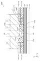
- FIG. 10 is a cross-sectional view showing the structure of the gate electrode of the semiconductor device according to the second embodiment.
- FIG. 11 is an enlarged cross-sectional view for explaining the shape of the sidewall of the semiconductor device according to the second embodiment.
- FIG. 12 is an enlarged cross-sectional view for explaining the shape of the lower surface of the protruding portion on the drain electrode side of the gate electrode of the semiconductor device according to the second embodiment.
- FIG. 13A is a cross-sectional view showing each step of the method for manufacturing a semiconductor device according to the second embodiment.
- FIG. 13B is a cross-sectional view showing each step of the method for manufacturing a semiconductor device according to the second embodiment.
- FIG. 13C is a cross-sectional view showing each step of the method for manufacturing a semiconductor device according to the second embodiment.
- FIG. 13D is a cross-sectional view showing each step of the method for manufacturing a semiconductor device according to the second embodiment.
- FIG. 13E is a cross-sectional view showing each step of the method for manufacturing a semiconductor device according to the second embodiment.
- FIG. 14 is an enlarged cross-sectional view for explaining the shape of the sidewall of the semiconductor device according to the first modification of the second embodiment.
- FIG. 15 is an enlarged cross-sectional view for explaining the shape of a sidewall of a semiconductor device according to a second modification of the second embodiment.
- FIG. 16 is an enlarged sectional view for explaining the shape of a sidewall of a semiconductor device according to a third modification of the second embodiment.
- FIG. 17 is an enlarged cross-sectional view for explaining the shape of a sidewall of a semiconductor device according to a fourth modification of the second embodiment.
- FIG. 18 is an enlarged sectional view for explaining the shape of a sidewall of a semiconductor device according to a fifth modification of the second embodiment.
- FIG. 19 is a cross-sectional view showing the structure of a conventional gate electrode.
- each figure is a schematic diagram and is not necessarily strictly illustrated.
- substantially the same configurations are denoted by the same reference numerals, and overlapping explanations will be omitted or simplified.
- the terms “upper” and “lower” in the configuration of a semiconductor device do not refer to the upper direction (vertically upward) or the downward direction (vertically downward) in absolute spatial recognition, but rather to the stacked structure. This is a term defined by the relative positional relationship based on the stacking order in . Additionally, the terms “above” and “below” are used not only when two components are spaced apart and there is another component between them; This also applies when two components are placed in close contact with each other.
- the X-axis, Y-axis, and Z-axis indicate three axes of a three-dimensional orthogonal coordinate system.
- two axes parallel to the main surface (top surface) of a substrate included in a semiconductor device are defined as an X-axis and a Y-axis
- a direction perpendicular to the main surface is defined as a Z-axis direction.
- the direction in which the source electrode, gate electrode, and drain electrode are lined up in this order, that is, the so-called gate length direction is set as the X-axis direction.
- the X-axis direction is an example of the first direction.
- the Z-axis direction is an example of the second direction.
- the Z-axis positive direction may be described as “upward” and the Z-axis negative direction may be described as “downward.”
- planar view refers to the main surface (upper surface) of the substrate of the semiconductor device viewed from the positive direction of the Z-axis.
- a group III nitride semiconductor is a semiconductor containing one or more types of group III elements and nitrogen.
- group III elements include aluminum (Al), gallium (Ga), and indium (In).
- group III nitride semiconductors include GaN, AlN, InN, AlGaN, InGaN, and AlInGaN.
- the Group III nitride semiconductor may contain one or more types of elements other than Group III, such as silicon (Si) and phosphorus (P).
- Si silicon
- P phosphorus
- a layer made of a group III nitride semiconductor and a layer composed of a group III nitride semiconductor mean that the layer substantially contains only a group III nitride semiconductor.
- the layer may contain other elements as impurities, such as elements that cannot be avoided during manufacturing, at a rate of 1 at % or less.
- the composition ratio (composition ratio) of group III elements of a nitride semiconductor refers to atoms of a target group III element among a plurality of group III elements contained in the nitride semiconductor. It represents the ratio of numbers.
- the Al composition ratio of the nitride semiconductor layer is a/(a+b+c ) can be expressed as
- the In composition ratio and the Ga composition ratio are represented by b/(a+b+c) and c/(a+b+c), respectively.
- ordinal numbers such as “first” and “second” do not mean the number or order of components, unless otherwise specified, and do not mean the number or order of components. It is used for the purpose of
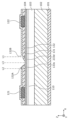
- FIG. 1 is a cross-sectional view showing the configuration of a semiconductor device 100 according to the first embodiment.
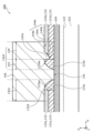
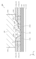
- FIG. 2 is an enlarged cross-sectional view showing the configuration of gate electrode 140 of semiconductor device 100 according to the first embodiment.
- FIG. 3 is an enlarged cross-sectional view for explaining the shape of the lower surface 144a of the projecting portion 142d on the drain electrode 122 side of the gate electrode 140 of the semiconductor device 100 according to the first embodiment. Note that FIGS.
- the semiconductor device 100 is a high electron mobility transistor (HEMT) having a Schottky junction gate structure.
- HEMT high electron mobility transistor
- the semiconductor device 100 includes a substrate 101, a buffer layer 102, a channel layer 103, a barrier layer 104, a two-dimensional electron gas 110, a source electrode 121, a drain electrode 122, and a source field. It includes a plate 123, a T-shaped gate electrode 140, an insulating layer 130, and a fourth insulating layer 134.
- the insulating layer 130 includes a first insulating layer 131, a second insulating layer 132, a first sidewall 133d, and a second sidewall 133s.
- the substrate 101 is, for example, a substrate made of Si.
- the substrate 101 is not limited to a substrate made of Si, but may be a substrate made of sapphire, SiC, GaN, AlN, or the like.
- the buffer layer 102 is provided above the substrate 101.
- the buffer layer 102 is provided in contact with the upper surface of the substrate 101.
- the buffer layer 102 is, for example, a layer made of a group III nitride semiconductor.
- the buffer layer 102 is composed of a plurality of stacked layers of AlN and AlGaN with a thickness of 2 ⁇ m.
- the buffer layer 102 may be composed of a single layer or multiple layers of a group III nitride semiconductor such as GaN, AlGaN, AlN, InGaN, and AlInGaN.
- the buffer layer 102 may not be provided.
- the channel layer 103 is provided above the substrate 101.
- the channel layer 103 is provided in contact with the upper surface of the buffer layer 102.
- Channel layer 103 is a layer made of a group III nitride semiconductor.
- the channel layer 103 is made of GaN with a thickness of 200 nm, for example.
- the channel layer 103 is not limited to GaN, and may be made of a group III nitride semiconductor such as InGaN, AlGaN, and AlInGaN.
- the channel layer 103 may contain an n-type impurity.
- the thickness of the channel layer 103 is not limited to the example described above.
- the barrier layer 104 is provided above the channel layer 103.
- the barrier layer 104 is provided in contact with the upper surface of the channel layer 103.
- the barrier layer 104 is a layer made of a group III nitride semiconductor having a larger band gap than the channel layer 103.
- the barrier layer 104 is made of, for example, AlGaN with a thickness of 20 nm and an Al composition ratio of 25%.
- a highly concentrated two-dimensional electron gas 110 is generated on the channel layer 103 side of the hetero interface between the barrier layer 104 and the channel layer 103.
- the two-dimensional electron gas 110 is used as a channel of a transistor.
- the barrier layer 104 is not limited to AlGaN, but may be made of a group III nitride semiconductor such as AlInGaN. Further, the barrier layer 104 may contain an n-type impurity. The thickness and Al composition ratio of the barrier layer 104 are not limited to the above example.
- a cap layer made of, for example, GaN and having a thickness of about 1 nm or more and about 2 nm or less may be provided on the barrier layer 104.
- a spacer layer made of, for example, AlN and having a thickness of about 1 nm may be provided between the channel layer 103 and the barrier layer 104 as a spacer layer. In this way, the channel layer 103 and the barrier layer 104 do not need to be in contact with each other.
- the source electrode 121 and the drain electrode 122 are provided above the barrier layer 104 with a space between them. Specifically, the source electrode 121 and the drain electrode 122 are provided to face each other with the gate electrode 140 interposed therebetween.
- the source electrode 121 and the drain electrode 122 are formed using a conductive material.
- the source electrode 121 and the drain electrode 122 are multilayer electrode films having a laminated structure in which a Ti film and an Al film are sequentially laminated, but the invention is not limited thereto.
- the source electrode 121 and the drain electrode 122 are not limited to a stacked structure of a Ti film and an Al film, but may be a transition metal, a transition metal nitride, or a carbide formed by sputtering.
- the source electrode 121 and the drain electrode 122 may be made of Ta, Hf, W, Ni, TiN, TaN, HfN, WN, TiC, TaC, HfC, Au, Cu, etc., or a compound containing these elements.
- it may be a multilayer electrode film consisting of a plurality of laminated structures.
- the source electrode 121 and the drain electrode 122 are electrically ohmically connected to the two-dimensional electron gas 110.
- the source electrode 121 and the drain electrode 122 there is a recessed portion where a part of the barrier layer 104 and/or the channel layer 103 is removed, or an n-type impurity containing a donor such as Si is formed.
- a contact layer containing the contact layer may be provided.
- the contact layer containing n-type impurities may be formed by, for example, plasma treatment, ion implantation, regrowth, or the like.
- the insulating layer 130 is provided above the barrier layer 104 between the gate electrode 140 and the source and drain electrodes 121 and 122. As shown in FIG. 1, the insulating layer 130 includes a first insulating layer 131, a second insulating layer 132, a first sidewall 133d, and a second sidewall 133s.
- the first insulating layer 131 is the lowest layer within the insulating layer 130.
- the first insulating layer 131 is provided above the barrier layer 104.
- the first insulating layer 131 is provided in contact with the upper surface of the barrier layer 104.
- the first insulating layer 131 is a layer made of silicon nitride.
- the first insulating layer 131 is made of Si 3 N 4 with a thickness of 50 nm.
- the first insulating layer 131 has a first opening 131A that penetrates the first insulating layer 131 and reaches the barrier layer 104 in a region where the source electrode 121 and the drain electrode 122 are provided. is provided.
- the first insulating layer 131 may have a stoichiometric structure in which the H content of Si 3 N 4 is low, for example. Thereby, electron trapping can be reduced and the second insulating layer 132 can be selectively removed by wet etching.
- the first insulating layer 131 is not limited to Si 3 N 4 and does not need to have stoichiometry, and may have a higher Si composition ratio or a higher N composition ratio than the stoichiometry. Further, the first insulating layer 131 may not be a single layer but may be a plurality of layers.
- the first insulating layer 131 of multiple layers Si 3 N 4 is used for the bottom layer and the upper layer controls the etch rate of wet etching, so the Si composition ratio may be higher than that of stoichiometry, or It may also be SiN with a high N composition ratio. Further, the first insulating layer 131 may be made of SiCN containing carbon.
- the second insulating layer 132 is provided above the first insulating layer 131. Specifically, the second insulating layer 132 is provided in contact with the upper surface of each of the first insulating layer 131, the source electrode 121, and the drain electrode 122.
- the second insulating layer 132 is a layer made of silicon oxide.
- the second insulating layer 132 is made of SiO 2 with a thickness of 50 nm. Note that the second insulating layer 132 is not limited to SiO 2 , as long as it has a lower dielectric constant than the first insulating layer 131 . Further, it is sufficient if the second insulating layer 132 can be selectively removed with respect to the first insulating layer 131.
- the second insulating layer 132 may be SiON containing oxygen in SiN, or may be a low-k film such as SiOC, SiOCH, or an organic film.
- a second opening 132A that penetrates the first insulating layer 131 and the second insulating layer 132 and reaches the barrier layer 104 is provided between the source electrode 121 and the drain electrode 122. It is provided.
- the second opening 132A has a width of 400 nm, for example. Note that the width of the second opening 132A may be in the range of 100 nm to 600 nm.
- the first insulating layer 131 and the second insulating layer 132 have a portion on the drain electrode 122 side and a portion on the source electrode 121 side. It can be divided into Specifically, the first insulating layer 131 includes a first insulating layer 131d on the drain electrode 122 side and a first insulating layer 131s on the source electrode 121 side. Further, the second insulating layer 132 includes a second insulating layer 132d on the drain electrode 122 side and a second insulating layer 132s on the source electrode 121 side.
- the upper surface shapes of the first insulating layer 131d and the second insulating layer 132d on the drain electrode 122 side are different from the upper surface shapes of the first insulating layer 131s and the second insulating layer 132s on the source electrode 121 side. There is. Specific differences in shape will be explained later.
- the present invention is not limited thereto, and at least one of the thickness and composition may be different.
- the thickness of the first insulating layer 131s may be thicker than the thickness of the first insulating layer 131d.
- the second insulating layer 132s and the second insulating layer 132d have the same thickness and layer composition, the present invention is not limited thereto, and at least one of the thickness and composition may be different.
- first insulating layer 131 when describing matters common to the first insulating layer 131s and the first insulating layer 131d, the description will be made as the first insulating layer 131. The same applies to the second insulating layer 132s and the second insulating layer 132d.
- the first sidewall 133d and the second sidewall 133s are provided between the barrier layer 104 and the protruding parts 142d and 142s of the gate electrode 140. Specifically, the first sidewall 133d and the second sidewall 133s are provided within the second opening 132A. More specifically, the first sidewall 133d is provided at the end of the insulating layer 130 between the junction 141 of the gate electrode 140 and the drain electrode 122 on the junction 141 side. The second sidewall 133s is provided at the end of the insulating layer 130 between the junction 141 and the source electrode 121 on the junction 141 side.
- first sidewall 133d is provided so as to be in contact with the side surface of the first insulating layer 131d on the bonding portion 141 side.
- the second sidewall 133s is provided so as to be in contact with the side surface of each of the first insulating layer 131s and the second insulating layer 132s on the joint portion 141 side.
- the first sidewall 133d and the second sidewall 133s are made of SiN with a width of 100 nm, for example.
- SiN generally has tensile stress.
- the opening portion of the second opening 132A can be substantially narrowed.
- the width of the exposed barrier layer 104 is 200 nm. becomes.
- the width of the first sidewall 133d and the second sidewall 133s may be set to any width from 20 nm to 200 nm.
- the first sidewall 133d and the second sidewall 133s may have different widths (lengths in the X-axis direction).
- first sidewall 133d may be formed using a high dielectric material. Thereby, the electric field at the drain electrode 122 side end of the portion where the gate electrode 140 and the barrier layer 104 are in contact (junction portion 141) can be further reduced. Further, the second sidewall 133s may be formed using a low dielectric material. As a result, the parasitic capacitance (gate-source capacitance Cgs) between the gate electrode 140 and the source electrode 121 can be reduced.
- the gate electrode 140 is provided with a space between the source electrode 121 and the drain electrode 122.
- the gate electrode 140 has a so-called T-shaped gate structure. Specifically, the gate electrode 140 covers the barrier layer 104 exposed on the bottom surface of the second opening 132A and a portion of the first insulating layer 131 and the second insulating layer 132 so as to cover the second opening 132A. It is located at the top.
- the gate electrode 140 includes a Schottky junction 141 with the barrier layer 104.
- bonding portion 141 is a contact surface where gate electrode 140 and barrier layer 104 come into contact.
- the joint portion 141 corresponds to a portion between the first sidewall 133d and the second sidewall 133s in plan view.
- the length of the joint portion 141 in the X-axis direction corresponds to the so-called gate length Lg.
- the gate length Lg can be shortened by the first sidewall 133d and the second sidewall 133s.
- the gate electrode 140 includes an overhanging portion that overhangs from the junction portion 141 to the source electrode 121 side and the drain electrode 122 side, respectively, when viewed in plan with respect to the main surface of the substrate 101.
- the gate electrode 140 has an overhanging portion 142s that extends toward the source electrode 121 side from the junction portion 141 in a plan view of the substrate 101, and a protrusion portion 142s that extends from the junction portion 141 in a plan view of the substrate 101.
- the overhanging parts 142d and 142s correspond to the arms of the T-shaped gate structure (the horizontal bar part of the T-shape), and the joint part 141 corresponds to the sole part of the T-shaped gate structure (the lower end of the vertical bar of the T-shape). do.
- the projecting portions 142d and 142s are located above the insulating layer 130 and do not contact the barrier layer 104.
- the lower surface of the projecting portion 142d on the drain electrode 122 side is not flat.
- the lower surface of the protruding portion 142d changes cubically. The specific shape of the lower surface of the projecting portion 142d will be described later.
- the gate electrode 140 is formed using a conductive material.
- the gate electrode 140 is, for example, a multilayer electrode film having a laminated structure in which a TiN film and an Al film are sequentially laminated.
- the thickness of the TiN film is 50 nm and the thickness of the Al film is 500 nm, but the thickness is not limited thereto.
- the gate electrode 140 is not limited to a stacked structure of a TiN film and an Al film, but may be a transition metal nitride or carbide formed by sputtering.
- the gate electrode 140 may be made of Ni, TiN, WN, HfN, TiC, WC, HfC, W, Au, Cu, etc., may be a compound containing these elements, or may have a multilayer structure. It may be a multilayer electrode film.
- the fourth insulating layer 134 is provided above the second insulating layer 132 and the gate electrode 140.
- the fourth insulating layer 134 is made of SiN with a thickness of 150 nm, for example. Note that the fourth insulating layer 134 is not limited to SiN, but may be SiO 2 or SiCN. Further, the stress of SiN constituting the fourth insulating layer 134 may be controlled by changing the Si composition ratio or the N composition ratio.
- the source field plate 123 is a source field plate provided above the gate electrode 140 and set to the same potential as the source electrode 121. Specifically, the source field plate 123 is provided above the fourth insulating layer 134. Source field plate 123 is provided so that at least a portion thereof is located between gate electrode 140 and drain electrode 122 in plan view. In the example shown in FIG. 1, the source field plate 123 is arranged so as to partially overlap the gate electrode 140 in plan view. The source field plate 123 is electrically insulated from the gate electrode 140 and the drain electrode 122, and is set to the potential applied to the source electrode 121 (source potential). By providing the source field plate 123, the electric field concentrated on the gate electrode 140 can be alleviated.
- the source field plate 123 is formed using a conductive material.
- the source field plate 123 has, for example, a multilayer electrode film structure having a laminated structure in which a TiN film and an Al film are sequentially laminated.
- the thickness of the TiN film is 50 nm and the thickness of the Al film is 500 nm, but the thickness is not limited thereto.
- the source field plate 123 is not limited to a stacked structure of a TiN film and an Al film, but may be a transition metal nitride or carbide formed by sputtering.
- the source field plate 123 may be made of Ti, Ta, W, Ni, TiN, TaN, WN, W, Au, Cu, etc., may be a compound containing these elements, or may be made of a plurality of laminated structures. It may also be a multilayer electrode film.
- the projecting portion 142d of the gate electrode 140 toward the drain electrode 122 includes a first gate field plate 143 and a second gate field plate 144.
- the first gate field plate 143 is an example of a first electric field plate, and is connected to the drain electrode 122 of the first sidewall 133d from a first position, which is the side end of the joint portion 141 of the first sidewall 133d in a plan view of the substrate 101. This is the section up to the second position, which is the side end. Note that the first position is also the position of the end of the portion where the gate electrode 140 and the barrier layer 104 are in contact (junction portion 141) on the side of the drain electrode 122.
- the first gate field plate 143 is a portion of the projecting portion 142d that is located directly above the first sidewall 133d, that is, a portion that overlaps the first sidewall 133d in plan view.
- the lower surface 143a of the first gate field plate 143 is in contact with the upper surface 133da of the first sidewall 133d.
- the upper surface 133da of the first sidewall 133d is curved to be convex upward.
- the lower surface 143a of the first gate field plate 143 is curved along the upper surface 133da.
- the lower surface 143a is inclined (curved) so that the distance from the barrier layer 104 increases monotonically toward the positive direction of the X-axis.
- the upper surface 133da and the lower surface 143a may be inclined planes or may be formed in a step-like shape.
- the upper surface 133sa of the second sidewall 133s may not be a curved surface, but may be an inclined plane, or may be formed in a step shape.
- the second gate field plate 144 is an example of a second electric field plate, and is a section from the second position in plan view of the substrate 101 to the third position, which is the end of the protruding portion 142d on the drain electrode 122 side.
- the second gate field plate 144 is a portion of the protruding portion 142d that is located directly above the first insulating layer 131, that is, a portion that overlaps with the first insulating layer 131 in plan view.
- a stacked first insulating layer 131d and second insulating layer 132d are provided between the second gate field plate 144 and the barrier layer 104.
- the lower surface 144a of the second gate field plate 144 includes a flat surface 144b, an inclined surface 144c, and a flat surface 144d. Note that the lower surface 144a does not need to include at least one of the flat surfaces 144b and 144d.
- the flat surface 144b is a plane (XY plane) parallel to the main surface of the substrate 101, and is in contact with the surface of the first insulating layer 131d. In this embodiment, the flat surface 144b is located below the interface between the first insulating layer 131d and the second insulating layer 132d, but the present invention is not limited thereto. The flat surface 144b may be flush with the interface between the first insulating layer 131d and the second insulating layer 132d.
- the inclined surface 144c is a surface whose distance from the barrier layer 104 monotonically increases toward the positive direction of the X-axis.
- the inclined surface 144c is in contact with the end surface of the second insulating layer 132d on the source electrode 121 side and the sidewall of the recess of the first insulating layer 131d.
- the inclined surface 144c is a plane inclined with respect to the main surface of the substrate 101.
- the inclined surface 144c may be a curved surface that is convex upward or downward.
- the angle of inclination (the angle made with respect to the XY plane) of the inclined surface 144c is not particularly limited, but is within a range of 45 degrees ⁇ 5 degrees, for example.
- the flat surface 144d is a plane (XY plane) parallel to the main surface of the substrate 101, and is in contact with the upper surface of the second insulating layer 132d.
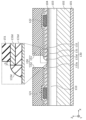
- the lower surface 144a having the above-mentioned shape can be defined by the elevation angle when viewed from the position P1 of the drain electrode 122 side end of the joint portion 141 of the gate electrode 140.
- the first elevation angle ⁇ 1 to the fifth elevation angle ⁇ 5 virtual lines VL1 to VL5 and positions P1 to P5 for defining each elevation angle will be explained using FIG.
- the first elevation angle ⁇ 1 to the fifth elevation angle ⁇ 5 are respectively the main surface of the substrate 101 when viewed from a predetermined position (point) to another predetermined position (point) or a predetermined direction in the cross-sectional view shown in FIG. (XY plane). Specifically, the first elevation angle ⁇ 1 to the fifth elevation angle ⁇ 5 are each expressed as an angle ( ⁇ 90°) formed by each of the virtual lines VL1 to VL5 shown in FIG. 3 and the main surface (XY plane) of the substrate 101. be done.
- the virtual line VL1 is a tangent to the upper surface 133da of the first sidewall 133d at the position P1.
- Virtual line VL2 is a straight line connecting position P1 and position P2.
- Virtual line VL3 is a straight line connecting position P1 and position P3.
- Virtual line VL4 is a straight line connecting position P1 and position P4.
- Virtual line VL5 is a straight line connecting position P3 and position P4.
- Position P1 is the end of the first sidewall 133d on the joint portion 141 side. Specifically, the position P1 is an example of a first position, and is also the end of the bonding portion 141 on the drain electrode 122 side.
- Position P2 is the highest position of the lower surface 143a of the first gate field plate 143. Specifically, position P2 is also the highest position of the upper surface 133da of the first sidewall 133d.
- Position P3 is the lowest end of the lower surface 144a (see FIG. 2) of the second gate field plate 144 on the side of the drain electrode 122. Specifically, position P3 is the end of the flat surface 144b on the drain electrode 122 side. In this embodiment, position P3 is also the lower end of inclined surface 144c.
- Position P4 is the highest end of the lower surface 144a (see FIG. 2) of the second gate field plate 144 on the drain electrode 122 side. Specifically, position P4 is the end of the flat surface 144d on the drain electrode 122 side.
- Position P5 is the upper end of the inclined surface 144c. In this embodiment, the position P5 is also the highest position of the lower surface 144a (see FIG. 2) of the second gate field plate 144 on the side of the joint portion 141.
- the second elevation angle ⁇ 2 is larger than the third elevation angle ⁇ 3.
- the lowest position (position P3) of the lower surface 144a of the second gate field plate 144 is lower than the highest position (position P2) of the first sidewall 133d.
- the lower surface of the projecting portion 142d of the gate electrode 140 on the drain electrode 122 side includes an inclined surface 144c that monotonically increases toward the drain electrode 122 side in the X-axis direction.
- the lowest position (P3) of the lower surface of the second gate field plate 144 is lower than the highest position (P2) of the upper surface 133da of the first sidewall 133d, when the transistor is off, the lower surface of the gate electrode 140 The depletion layer tends to spread toward the drain electrode 122 side. Therefore, when the voltage applied between the gate electrode 140 and the drain electrode 122 is low, the position of the two-dimensional electron gas 110 is closer to the drain electrode 122 side than in the conventional technology, that is, when the voltage applied between the gate electrode 140 and the drain electrode 122 is low. located away from. This reduces the area where the two-dimensional electron gas 110 and the gate electrode 140 face each other.
- the distance between the two-dimensional electron gas 110 and the first gate field plate 143 can be increased, so that the parasitic capacitance (gate-drain capacitance Cgd) can be reduced.
- the semiconductor device 100 according to the present embodiment it is possible to achieve both reduction in electric field strength and reduction in parasitic capacitance.
- the overhanging portion 142s on the source electrode 121 side is not located below the highest position (position P2) of the first sidewall 133d in a portion closer to the source electrode 121 than the second sidewall 133s. . By doing so, an increase in parasitic capacitance between the gate electrode 140 and the source electrode 121 can be suppressed.
- the fifth elevation angle ⁇ 5 is smaller than the second elevation angle ⁇ 2.
- the slope from position P3 to position P4 can be made gentler. Therefore, the electric field at the lowest end of the lower surface 144a of the second gate field plate 144 on the side of the drain electrode 122 (position P3) can be relaxed and the undulations of the electric field can be reduced.
- At least one of the first insulating layer 131d and the second insulating layer 132s may be thinner than the first insulating layer 131s and the second insulating layer 132s on the source electrode 121 side. By doing so, the electric field strength can be further reduced by dispersing local electric field concentration at the drain electrode 122 side end portion (position P1) where the junction portion 141 of the gate electrode 140 and the barrier layer 104 are in contact.
- the semiconductor device 100 includes the substrate 101, the channel layer 103 made of a group III nitride semiconductor provided above the substrate 101, and the channel layer 103 provided above the channel layer 103.
- a barrier layer 104 made of a group III nitride semiconductor having a larger bandgap than the channel layer 103; a source electrode 121 and a source electrode 121 provided above the barrier layer 104 and spaced apart from each other in the X-axis direction on the main surface of the substrate 101;
- a drain electrode 122, a gate electrode 140 provided with a space between the source electrode 121 and the drain electrode 122 in the X-axis direction, and a gate electrode 140, the source electrode 121, and the drain electrode 122.
- the insulating layer 130 includes a first insulating layer 131 made of silicon nitride as the lowermost layer, and a second insulating layer 132 made of silicon oxide above the first insulating layer 131.
- the gate electrode 140 has a junction 141 that is Schottky-junctioned with the barrier layer 104, and overhanging parts 142s and 142d that extend from the junction 141 toward the source electrode 121 side and the drain electrode 122 side, respectively, in the X-axis direction. include.
- the insulating layer 130 is formed between the protruding portion 142d and the barrier layer 104 in the Z-axis direction perpendicular to the main surface of the substrate 101, and at the side end of the insulating layer 130 between the bonding portion 141 and the drain electrode 122 (
- the first sidewall 133d is provided at the end of the insulating layer 130 between the joint 141 and the source electrode 121 on the joint 141 side (the end on the joint 141 side). and a second sidewall 133s.
- the overhanging portion 142d is a first gate field in a section from a first position, which is the end of the first sidewall 133d on the side of the joint portion 141, to a second position, which is the end of the first sidewall 133d on the side of the drain electrode 122, in a plan view. It includes a plate 143 and a second gate field plate 144 in the section from the second position to the third position, which is the end of the projecting portion 142d on the side of the drain electrode 122 in plan view.
- a stacked first insulating layer 131d and a second insulating layer 132d are provided between the second gate field plate 144 and the barrier layer 104.
- a tangent line (virtual line VL1) at the first position (position P1) of the upper surface 133da of the first sidewall 133d has an inclination of a first elevation angle ⁇ 1 with respect to the main surface
- the highest position (position P2) of the lower surface 143a of the first gate field plate 143 is at a second elevation angle ⁇ 2 with respect to the main surface of the substrate 101 when viewed from the first position.
- the lowest drain electrode 122 side end (position P3) of the lower surface 144a of the second gate field plate 144 has an inclination of a third elevation angle ⁇ 3 with respect to the main surface of the substrate 101 when viewed from the first position.
- the second elevation angle ⁇ 2 is larger than the third elevation angle ⁇ 3.
- the lower surface 144a of the second gate field plate 144 includes an inclined surface 144c whose distance from the barrier layer 104 increases monotonically in the direction from the gate electrode 140 to the drain electrode 122.
- two-dimensional electron gas 110 is generated in the channel layer 103 near the interface with the barrier layer 104, so it is possible to realize a transistor that uses the generated two-dimensional electron gas 110 as a channel.
- the gate electrode 140 since the gate electrode 140 includes the bonding portion 141 and the overhanging portion 142d, it becomes easier to realize miniaturization of the gate length (Lg) and relaxation of the electric field by the overhanging portion 142d.
- the lowest position (position P3) of the lower surface 144a of the second gate field plate 144 is located below the highest position (position P2) of the lower surface 143a of the first gate field plate 143. Further, the lower surface 144a of the second gate field plate 144 includes a monotonically increasing slope 144c.
- the electric field can be dispersed to the drain electrode 122 side end of the second gate field plate 144 (position P4), the lowest position of the lower surface 144a of the second gate field plate 144 (position P3), and the inclined surface 144c, Electric field concentration can be alleviated.
- the second elevation angle ⁇ 2 is larger than the third elevation angle ⁇ 3, the first sidewall 133d becomes thicker. This makes it easier to ensure a long distance between the two-dimensional electron gas 110 and the protruding portion 142d of the gate electrode 140, so that parasitic capacitance (gate-drain capacitance Cgd) can be reduced.
- a laminated film of the first insulating layer 131d and the second insulating layer 132d is provided between the second gate field plate 144 and the barrier layer 104. Since the second insulating layer 132d is made of a silicon oxide film having a lower dielectric constant than the silicon nitride film forming the first insulating layer 131d, parasitic capacitance (gate-drain capacitance Cgd) can be reduced. Thus, according to the above configuration, both electric field relaxation and parasitic capacitance reduction can be achieved.
- the first insulating layer 131, the first sidewall 133d, and the second sidewall 133s made of a silicon nitride film can compensate for nitrogen vacancies in the barrier layer 104 and reduce the interface state. Therefore, off-leakage current between the gate electrode 140 and the drain electrode 122 can be reduced.
- the protruding portion 142s closer to the source electrode 121 than the second sidewall 133s is not located below the highest position (position P2) of the upper surface 133da of the first sidewall 133d.
- the elevation angle with respect to the main surface of the substrate 101 when looking at the side end of the drain electrode 122 at the highest position (position P4) is a fifth elevation angle ⁇ 5
- the fifth elevation angle ⁇ 5 is smaller than the second elevation angle ⁇ 2.
- the slope from position P3 to position P4 can be made gentler. Therefore, the electric field at the lowest end of the lower surface 144a of the second gate field plate 144 on the side of the drain electrode 122 (position P3) can be relaxed and the undulations of the electric field can be reduced.
- the inclined surface included in the lower surface 144a of the second gate field plate 144 has at least one inclined surface whose inclination angle with respect to the main surface of the substrate 101 is within the range of 45 degrees ⁇ 5 degrees. Including surface 144c.
- the shape of the top surface of the insulating layer 130 can be easily formed using an isotropic etching method such as wet etching. Since the lower surface shape of the protruding portion 142d of the gate electrode 140 follows the upper surface shape of the insulating layer 130, manufacturing variations in the gate electrode 140 are reduced and a highly reliable device can be realized.
- At least one of the flat surface 144b and the flat surface 144d may be inclined.
- the slope may be such that the distance from the barrier layer 104 increases or decreases in the positive direction of the X axis. Further, the slope may be flat or curved.
- FIGS. 4E and 4F also each show an enlarged view of a portion near the first sidewall 133d.
- FIGS. 4A to 4D three lines L1 to L3 extending in the Z-axis direction from the top surface of the barrier layer 104 are shown as dashed-dotted lines in order to make it easier to understand the positional relationship between the figures.
- the line L1 represents the position of the end of the first sidewall 233d on the drain electrode 122 side.
- Line L2 represents the position of the source electrode 121 side end of the second sidewall 133s.
- Line L3 represents the center position of joint portion 141.
- a layered structure of AlN and AlGaN with a thickness of 2 ⁇ m is deposited on a substrate 101 made of Si using metal organic chemical vapor deposition (MOCVD).
- MOCVD metal organic chemical vapor deposition
- a buffer layer 102, a channel layer 103 having a thickness of 200 nm and made of GaN, and a barrier layer 104 having a thickness of 20 nm and made of AlGaN with an Al composition ratio of 25% are epitaxially grown in sequence in the +c plane direction ( ⁇ 0001> direction). is formed.
- a highly concentrated two-dimensional electron gas 110 is generated on the channel layer 103 side of the hetero interface between the barrier layer 104 and the channel layer 103, and a channel of the two-dimensional electron gas 110 is formed.
- a first insulating layer 131, a source electrode 121 and a drain electrode 122, and a second insulating layer 132 are formed.
- a first insulating layer 131 made of Si 3 N 4 with a thickness of 50 nm is deposited by a low pressure CVD (Chemical Vapor Deposition) method.
- the resist is patterned by a lithography method, thereby forming a mask in areas other than the regions where the source electrode 121 and the drain electrode 122 are to be formed.
- a dry etching method is used to form a first opening 131A in the first insulating layer 131 so that the barrier layer 104 is exposed, and then the mask and polymer are removed. Note that although a dry etching method is used in this embodiment, the first opening 131A may be formed in the first insulating layer 131 using a wet etching method.
- a source electrode 121 and a drain electrode 122 are formed by a lift-off method.
- the two-dimensional electron gas 110 and each of the source electrode 121 and the drain electrode 122 are electrically ohmically connected.
- the source electrode 121 and the drain electrode 122 may be formed by sequentially applying a lithography method and a dry etching method after sequentially depositing a Ti film and an Al film by a sputtering method.
- the second insulating layer 132 is formed on the first insulating layer 131 and the source electrode 121 and drain electrode 122.
- the second insulating layer 132 is formed by depositing SiO 2 with a thickness of 50 nm by plasma CVD.
- a second opening 132A and a third insulating layer 133 are formed. Specifically, first, a resist is applied, and then the resist is patterned by a lithography method to form a mask in a region other than the region where the second opening 132A is to be formed. Next, a dry etching method is used to form second openings 132A in the first insulating layer 131 and the second insulating layer 132 so that the barrier layer 104 is exposed. After the second opening 132A is formed, the mask and polymer are removed.
- a third insulating layer 133 made of SiN and having a thickness of 100 nm is deposited by plasma CVD.
- the third insulating layer 133 is provided to fill the second opening 132A.
- the third insulating layer 133 is etched back using a dry etching method. As a result, the first sidewall 133d and the second sidewall 133s are formed so that the barrier layer 104 is exposed.
- the resist is patterned by a lithography method to form a mask (resist pattern 150).
- the mask is formed to expose the first sidewall 133d and the second sidewall 133s.
- the resist pattern 150 includes a mask portion 151 on the drain electrode 122 side and a mask portion 152 on the source electrode 121 side.
- the end of the mask portion 151 of the resist pattern 150 is located closer to the drain electrode 122 than the end of the first sidewall 133d on the drain electrode 122 side. That is, the mask portion 151 is arranged to expose the end of the second insulating layer 132d on the source electrode 121 side and the vicinity thereof. As shown in an enlarged view in FIG. 4E, the distance D between the end of the mask portion 151 on the source electrode 121 side and the end of the first sidewall 133d on the drain electrode 122 side is ensured at a distance greater than 0. ing.
- the end of the mask portion 152 of the resist pattern 150 is located closer to the drain electrode 122 than the end of the second sidewall 133s on the source electrode 121 side. That is, the mask portion 152 is positioned so as to completely cover the second insulating layer 132s and partially cover the second sidewall 133s. Note that in this embodiment, the end of the mask portion 152 on the drain electrode 122 side may coincide with the end of the second sidewall 133s on the source electrode 121 side in plan view. Further, the end of the mask portion 152 may be located above the barrier layer 104.
- a part of the second insulating layer 132d (specifically, a part near the end on the first sidewall 133d side) is removed.
- a wet etching method is used to selectively remove a portion of the second insulating layer 132d exposed from the mask portion 151 on the drain electrode 122 side, and then the resist pattern 150 is removed.
- a part of the second insulating layer 132d is selectively removed using BHF (Buffered Hydrofluoric acid) at room temperature. Note that an arbitrary mixing ratio of BHF may be used, or a portion of the second insulating layer 132d may be selectively removed using DHF (Diluted Hydrofluoric Acid).
- etching proceeds isotropically from the gap between the first sidewall 133d and the mask portion 151. Therefore, as shown in FIG. 4F, the end of the second insulating layer 132d on the source electrode 121 side becomes an obliquely inclined surface.
- the first insulating layer 131 and the third insulating layer 133 are made of SiN, and the second insulating layer 132 is made of SiO2 , and the second insulating layer 132 is selectively removed by wet etching using BHF.
- BHF wet etching
- any combination of insulating materials may be used as long as the second insulating layer 132 can be selectively removed.
- a wet etching method is used, the first insulating layer 131 and the third insulating layer 133 are made of SiO 2 and the second insulating layer 132 is made of SiN, and a chemical dry etching method may be used.
- a gate electrode 140 is formed. Specifically, TiN with a thickness of 50 nm and Al with a thickness of 450 nm are sequentially deposited by sputtering. Thereafter, a resist is applied to a region where the gate electrode 140 is to be formed, and then a lithography method is used to pattern the resist to form a mask. A dry etching method is then used to remove the mask and polymer after gate electrode 140 is formed.
- a fourth insulating layer 134 made of SiN with a thickness of 150 nm is deposited by plasma CVD, and then TiN with a thickness of 50 nm and Al with a thickness of 450 nm are sequentially deposited by a sputtering method.
- a resist is applied to a region where the source field plate 123 is to be formed, and then a lithography method is used to pattern the resist to form a mask. A dry etching method is then used to remove the mask and polymer after source field plate 123 is formed.
- the shape of the lower surface of the protruding portion 142d of the gate electrode 140 on the drain electrode 122 side is different from that in the first embodiment.
- the explanation will focus on the differences from Embodiment 1, and the explanation of the common points will be omitted or simplified.
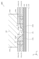
- FIG. 5 is a cross-sectional view showing the configuration of the gate electrode 140 of the semiconductor device 100A according to the first modification of the first embodiment.
- FIG. 6 is an enlarged cross-sectional view for explaining the shape of the lower surface 144a of the gate electrode 140 of the semiconductor device 100A according to the first modification of the first embodiment, the projecting portion 142d toward the drain electrode 122 side.
- the lower surface 144a of the second gate field plate 144 includes an inclined surface 144c and a flat surface 144d.
- the lower surface 144a does not include the flat surface 144b shown in FIG.
- the second insulating layer 132 is located below the lowest position (position P3 shown in FIG. 6) on the lower surface 144a of the second gate field plate 144.
- the first sidewall 133d is provided so as to be in contact with the side surface of each of the first insulating layer 131d and the second insulating layer 132d on the joint portion 141 side.
- the third elevation angle ⁇ 3 is larger than the fourth elevation angle ⁇ 4.
- the distance between the lowest drain electrode 122 side end (position P3) of the lower surface 144a of the second gate field plate 144 and the two-dimensional electron gas 110 can be increased, so that the electric field strength at position P3 can be reduced.
- the second insulating layer 132 made of SiO 2 has a lower dielectric constant than the first insulating layer 131 made of SIN, the electric field strength at the position P3 can be reduced, and the parasitic capacitance (gate-drain capacitance Cgd) can be reduced. can be reduced.
- the semiconductor device 100A in the cross section shown in FIG. 6, from the first position (position P1) to the drain electrode 122 side end ( If the elevation angle with respect to the main surface of the substrate 101 when looking at position P4) is a fourth elevation angle ⁇ 4, the third elevation angle ⁇ 3 is larger than the fourth elevation angle ⁇ 4.
- the distance between the lowest position (position P3) of the lower surface 144a of the second gate field plate 144 and the two-dimensional electron gas 110 can be increased, so that the electric field concentration at the position P3 can be alleviated, and the parasitic capacitance can be reduced. (gate-drain capacitance Cgd) can be reduced.
- the second insulating layer 132d overlaps the lowest position of the lower surface 144a of the second gate field plate 144 in plan view.
- the second insulating layer 132d made of a silicon oxide film with a low dielectric constant, electric field concentration at the position P3 can be alleviated, and parasitic capacitance (gate-drain capacitance Cgd) can be reduced. can do.
- the lower surface 144a of the second gate field plate 144 does not need to include the flat surface 144d.
- the lower surface 144a of the second gate field plate 144 may include a flat surface located closer to the first sidewall 133d than the position P3.
- the lower surface 144a may be provided with a flat surface extending from position P3 along the negative direction of the X-axis. The flat surface is located above the flat surface 144b shown in FIG. 2, and a portion of the second insulating layer 132d is provided below the flat surface. Therefore, it is possible to both alleviate electric field concentration and reduce parasitic capacitance.
- FIG. 7 is a cross-sectional view showing the configuration of the gate electrode 140 of the semiconductor device 100B according to the second modification of the first embodiment.
- FIG. 8 is an enlarged sectional view for explaining the shape of the lower surface 144a of the gate electrode 140 of the semiconductor device 100B according to the second modification of the first embodiment, the projecting portion 142d toward the drain electrode 122 side.
- the lower surface 144a of the second gate field plate 144 includes three flat surfaces 144b, 144d and 144f and two inclined surfaces 144c and 144e. Specifically, the flat surface 144b, the sloped surface 144e, the flat surface 144f, the sloped surface 144c, and the flat surface 144d are lined up in this order toward the positive direction of the X-axis. The flat surface 144b is located below the flat surface 144f, and the flat surface 144f is located below the flat surface 144d. That is, the lower surface 144a is provided in a stepped shape. The flat surface 144b, the inclined surface 144e, and the flat surface 144f are in contact with the first insulating layer 131d.
- the inclined surface 144c and the flat surface 144d are in contact with the second insulating layer 132d.
- the slope angles of the slopes 144c and 144e are the same, but may be different.
- the angle of inclination of each of the inclined surfaces 144c and 144e is within the range of 45 degrees ⁇ 5 degrees.
- the third elevation angle ⁇ 3 is smaller than the fourth elevation angle ⁇ 4. That is, the lowest end of the lower surface 144a of the second gate field plate 144 on the side of the drain electrode 122 (position P3) is located below the virtual line VL4. Thereby, the distance between the position P3 and the two-dimensional electron gas 110 can be shortened, so that the electric field strength at the side end of the drain electrode 122 (position P1) where the gate electrode 140 and the barrier layer 104 are in contact can be reduced.
- the first insulating layer 131d made of SiN has a higher dielectric constant than the second insulating layer 132d made of SiO2 . Therefore, the electric field strength at the side end of the drain electrode 122 (position P1) where the gate electrode 140 and the barrier layer 104 are in contact can be further reduced. Therefore, the depletion layer tends to spread to the drain electrode 122 side below the gate electrode 140, so that the short channel effect can be suppressed.
- the semiconductor device 100B in the cross section shown in FIG. 8, from the first position (position P1) to the drain electrode 122 side end ( If the elevation angle with respect to the main surface of the substrate 101 when looking at position P4) is a fourth elevation angle ⁇ 4, the fourth elevation angle ⁇ 4 is larger than the third elevation angle ⁇ 3.
- the lowest position (position P3) of the lower surface 144a of the second gate field plate 144 approaches the two-dimensional electron gas 110, which alleviates the concentration of electric field on the drain electrode 122 side end (position P1) of the junction 141. I can do it.
- the lower surface 144a of the second gate field plate 144 contacts the first insulating layer 131d.
- the lowest position (position P3) of the lower surface 144a of the second gate field plate 144 approaches the two-dimensional electron gas 110, which alleviates the concentration of electric field on the drain electrode 122 side end (position P1) of the junction 141. I can do it.
- the depletion layer tends to spread toward the drain electrode 122 below the gate electrode 140, and short channel effects can be suppressed.
- FIG. 9 is an enlarged sectional view for explaining the positional relationship between the shape of the lower surface of the gate electrode 140 and the source field plate 123 of the semiconductor device 100C according to the third modification of the first embodiment.
- the third elevation angle ⁇ 3 is equal to the fourth elevation angle ⁇ 4.
- the third elevation angle ⁇ 3 becomes equal to the fifth elevation angle ⁇ 5. That is, the virtual line VL3 matches each of the virtual lines VL4 and VL5.
- the lower surface 144a of the second gate field plate 144 becomes a slope that monotonically increases from position P3 to position P4.
- the electric field strength can be reduced.
- the fifth elevation angle ⁇ 5 may be within the range of 45 degrees ⁇ 5 degrees.
- the fifth elevation angle ⁇ 3 matches the inclination angle of the lower surface 144a, which is an inclined surface.
- the shape of the lower surface 144a of the second gate field plate 144 is formed by partially etching the second insulating layer 132d. In this case, since an isotropic etching method can be used, the shape of the lower surface 144a can be easily formed.
- the source field plate 123 does not protrude below the virtual line VL4. Specifically, the surface of source field plate 123 touches virtual line VL4. More specifically, the end of the lower surface of the source field plate 123 on the side of the drain electrode 122 (position P6) is in contact with the virtual line VL4.
- the electric field strength at the end of the source field plate 123 on the side of the drain electrode 122 (position P6) can be reduced. Further, the electric field applied to each of the end of the source field plate 123 on the drain electrode 122 side (position P6) and the end of the gate electrode 140 on the drain electrode 122 side (positions P1, P3, and P4) can be made uniform.
- the semiconductor device 100C in the cross section shown in FIG. 9, from the first position (position P1) to the drain electrode 122 side end ( If the elevation angle with respect to the main surface of the substrate 101 when looking at position P4) is a fourth elevation angle ⁇ 4, the fourth elevation angle ⁇ 4 is equal to the third elevation angle ⁇ 3.
- the electric field applied to the gate electrode 140 can be made uniform, and the effect of alleviating electric field concentration can be enhanced.
- the semiconductor device 100C includes a source field plate 123 provided above the gate electrode 140 and set to the same potential as the source electrode 121.
- the source field plate 123 is located along a virtual line VL4 connecting the first position (position P1) and the highest position side end of the drain electrode 122 on the lower surface 144a of the second gate field plate 144 (position P4). Do not protrude downward.
- the electric field concentrated on the gate electrode 140 can be relaxed by the source field plate 123. Further, since the source field plate 123 does not protrude below the virtual line VL4, local electric field concentration on the source field plate 123 can be alleviated. Thereby, parasitic capacitance (source-drain capacitance Cds) can be reduced.
- the surface of the source field plate 123 is in contact with the virtual line VL4 in the cross section shown in FIG.
- the electric field applied to the gate electrode 140 and the source field plate 123 can be made uniform, and the effect of alleviating electric field concentration can be enhanced.
- the second embodiment is different from the first embodiment in that the sidewall on the drain electrode side and the sidewall on the source electrode side have different heights.
- the explanation will focus on the differences from Embodiment 1, and the explanation of the common points will be omitted or simplified.
- FIG. 10 is an enlarged cross-sectional view showing the configuration of the gate electrode 140 of the semiconductor device 200 according to the second embodiment.
- FIG. 11 is an enlarged cross-sectional view for explaining the shape of the sidewall of the semiconductor device 200 according to the second embodiment.
- the first sidewall 133d on the drain electrode 122 side is replaced with a The difference is that one sidewall 233d is provided.
- the highest position of the upper surface 233da of the first sidewall 233d is located below the highest position of the upper surface 133sa of the second sidewall 133s.
- the first sidewall 233d is shorter (shorter in the Z-axis direction) than the second sidewall 133s.
- the first sidewall 233d may have a smaller width than the second sidewall 133s.
- the highest position of the upper surface 233da of the first sidewall 233d is indicated by a position P2.
- the height of the first sidewall 233d is the distance between the upper surface of the barrier layer 104 and the position P2, and is expressed as HSWd .
- the highest position of the upper surface 133sa of the second sidewall 133s is represented by a position P7.
- the height of the second sidewall 133s is the distance between the upper surface of the barrier layer 104 and the position P7, and is expressed by HSWs .
- H SWd ⁇ H SWs is satisfied. Note that in this embodiment, the "height" represents the distance from the top surface of the barrier layer 104 in the Z-axis direction unless otherwise specified.
- the thickness of the insulating layer 130 on the side of the drain electrode 122 that is, the thickness of the stacked structure of the first insulating layer 131d and the second insulating layer 132d is expressed as HFPd .
- the thickness HFPd corresponds to the height of the highest position of the lower surface of the projecting portion 142d of the gate electrode 140 toward the drain electrode 122 side.
- the thickness of the first insulating layer 131d is expressed as H I.
- the thickness of the insulating layer 130 on the source electrode 121 side that is, the thickness of the stacked structure of the first insulating layer 131s and the second insulating layer 132s is expressed as HFPs .
- the thickness HFPs corresponds to the height of the highest position of the lower surface of the projecting portion 142s of the gate electrode 140 toward the source electrode 121 side.
- H SWd ⁇ H I holds true. That is, the highest position P2 of the first sidewall 233d is located at a position lower than the interface between the first insulating layer 131d and the second insulating layer 132d. Specifically, the highest position P2 of the first sidewall 233d is at the same height as the upper surface of the first insulating layer 131d (the portion that contacts the flat surface 144b of the projecting portion 142d). Therefore, the upper surface of the first insulating layer 131d smoothly continues from the upper surface 233da of the first sidewall 233d.
- the lower surface 143a of the first gate field plate 143 and the lower surface 144a (specifically, the inclined surface 144c) of the second gate field plate 144 are smoothly continuous on the lower surface of the projecting portion 142d of the gate electrode 140. .
- the coverage of the gate electrode 140 can be improved, and the reliability of the device can be improved.
- the lower surface 144a of the second gate field plate 144 includes an inclined surface 144c whose distance from the barrier layer 104 monotonically increases in the positive direction of the X-axis, as in the first embodiment. I'm here.
- the semiconductor device 200 includes the substrate 101, the channel layer 103 made of a group III nitride semiconductor provided above the substrate 101, and the channel layer 103 provided above the channel layer 103.
- a barrier layer 104 made of a group III nitride semiconductor having a larger bandgap than the channel layer 103; a source electrode 121 and a source electrode 121 provided above the barrier layer 104 and spaced apart from each other in the X-axis direction on the main surface of the substrate 101;
- a drain electrode 122, a gate electrode 140 provided with a space between the source electrode 121 and the drain electrode 122 in the X-axis direction, and a gate electrode 140, the source electrode 121, and the drain electrode 122.
- the insulating layer 130 includes a first insulating layer 131 made of silicon nitride as the lowermost layer, and a second insulating layer 132 made of silicon oxide above the first insulating layer 131.
- the gate electrode 140 has a junction 141 that is Schottky-junctioned with the barrier layer 104, and overhanging parts 142s and 142d that extend from the junction 141 toward the source electrode 121 side and the drain electrode 122 side, respectively, in the X-axis direction. include.
- the insulating layer 130 is formed between the protruding portion 142d and the barrier layer 104 in the Z-axis direction perpendicular to the main surface of the substrate 101, and at the side end of the insulating layer 130 between the bonding portion 141 and the drain electrode 122 (
- the first sidewall 233d is provided at the end of the insulating layer 130 between the joint 141 and the source electrode 121 on the joint 141 side (the end on the joint 141 side). and a second sidewall 133s.
- the overhanging portion 142d is a first gate field in a section from a first position, which is the end of the first sidewall 233d on the side of the joint portion 141, to a second position, which is the end of the first sidewall 233d on the side of the drain electrode 122, in a plan view. It includes a plate 143 and a second gate field plate 144 in the section from the second position to the third position, which is the end of the projecting portion 142d on the side of the drain electrode 122 in plan view.
- a stacked first insulating layer 131d and a second insulating layer 132d are provided between the second gate field plate 144 and the barrier layer 104.
- a tangent line (virtual line VL1) at the first position (position P1) of the upper surface 133da of the first sidewall 133d has an inclination of a first elevation angle ⁇ 1 with respect to the main surface
- the highest position (position P2) of the lower surface 143a of the first gate field plate 143 is at a second elevation angle ⁇ 2 with respect to the main surface of the substrate 101 when viewed from the first position.
- the lowest drain electrode 122 side end (position P3) of the lower surface 144a of the second gate field plate 144 has an inclination of a third elevation angle ⁇ 3 with respect to the main surface of the substrate 101 when viewed from the first position.
- the highest position (position P2) of the upper surface 233da of the first sidewall 233d is located below the highest position (position P7) of the upper surface 133da of the second sidewall 133s.
- two-dimensional electron gas 110 is generated in the channel layer 103 near the interface with the barrier layer 104, so it is possible to realize a transistor that uses the generated two-dimensional electron gas 110 as a channel.
- the gate electrode 140 since the gate electrode 140 includes the bonding portion 141 and the overhanging portion 142d, it becomes easier to realize miniaturization of the gate length (Lg) and relaxation of the electric field by the overhanging portion 142d.
- the semiconductor device 200 since the height of the first sidewall 233d is reduced, the distance between the first gate field plate 143 and the two-dimensional electron gas 110 is shortened. Therefore, when the transistor is off, the depletion layer in the channel layer 103 can spread easily, and the short channel effect can be suppressed. Therefore, the off-leakage current between the source electrode 121 and the drain electrode 122 can be suppressed, and the off-state characteristics of the semiconductor device 200 can be improved.
- the height of the second sidewall 133s is high, the electron density of the two-dimensional electron gas 110 below the second sidewall 133s is high. Therefore, the parasitic resistance between the gate electrode 140 and the source electrode 121 can be made low, so that the on-resistance can be made low.
- the semiconductor device 200 according to the present embodiment it is possible to achieve both lower on-resistance and improved off-resistance.
- the lower surface 144a of the second gate field plate 144 has an inclined surface 144c whose distance from the barrier layer 104 monotonically increases in the direction from the gate electrode 140 to the drain electrode 122.
- the electric field can be dispersed to the end of the gate electrode 140 on the drain electrode 122 side and the lowest position (position P3) of the lower surface 144a of the second gate field plate 144, and electric field concentration can be alleviated.
- FIG. 12 is an enlarged cross-sectional view for explaining the shape of the lower surface 144a of the overhanging portion 142d on the drain electrode 122 side of the gate electrode 140 of the semiconductor device 200 according to the present embodiment.
- first elevation angle ⁇ 1 to fifth elevation angle ⁇ 5 are defined.
- the first elevation angle ⁇ 1 to the fifth elevation angle ⁇ 5 are respectively the same as in the semiconductor device 100 according to the first embodiment, and are defined by virtual lines VL1 to VL5 and positions P1 to P5.
- the second elevation angle ⁇ 2 is larger than the third elevation angle ⁇ 3. Further, the second elevation angle ⁇ 2 is larger than the fifth elevation angle ⁇ 5. The third elevation angle ⁇ 3 is larger than the fourth elevation angle ⁇ 4. As a result, as in the first embodiment, electric field relaxation and parasitic capacitance reduction can be achieved.
- the second elevation angle ⁇ 2 may be smaller than the third elevation angle ⁇ 3 (semiconductor device 200B in FIG. 15). Further, although not shown in the figure, the second elevation angle ⁇ 2 may be equal to the third elevation angle ⁇ 3. Further, the third elevation angle ⁇ 3 may be smaller than the fourth elevation angle ⁇ 4. Further, the third elevation angle ⁇ 3, the fourth elevation angle ⁇ 4, and the fifth elevation angle ⁇ 5 may be equal. In this way, also in this embodiment, the modifications related to each elevation angle described in Embodiment 1 and its modifications can be applied.
- FIGS. 13A to 13E are cross-sectional views for explaining each structure of the method for manufacturing semiconductor device 200 according to this embodiment.
- 13A to 13E each show a cross-sectional configuration of the semiconductor device 200 in the middle of manufacturing.
- the three lines L1 to L3 extending in the Z-axis direction from the top surface of the barrier layer 104 shown in each figure are the same as the lines L1 to L3 shown in FIG. 4A, respectively.
- the steps up to forming the second insulating layer 132 are the same as in the first embodiment. That is, by the process described using FIGS. 4A and 4B, the buffer layer 102, the channel layer 103, the barrier layer 104, the first insulating layer 131, the source electrode 121, the drain electrode 122, and the second insulating layer are formed above the substrate 101. Layer 132 is formed.
- a resist pattern 250 with openings in predetermined regions is formed. Specifically, after the resist is applied, the resist is patterned by lithography to form a mask (resist pattern 250) in a region other than the region where the third opening 132B (see FIG. 13B) is to be formed.
- the opening provided in the resist pattern 250 is formed, for example, by removing the range between the line L1 and the line L3.
- the mask (resist pattern 250) is removed after the third opening 132B is formed by selectively removing the second insulating layer 132 using a wet etching method.
- a portion of the second insulating layer 132 is selectively removed using BHF at room temperature. Note that any mixing ratio of BHF may be used, and the second insulating layer 132 may be selectively removed using DHF.
- the first insulating layer 131 is made of SiN and the second insulating layer 132 is made of SiO2 , and the second insulating layer 132 is selectively removed by wet etching using BHF. Not exclusively. Any combination that allows selective removal of the second insulating layer 132 may be used. Although a wet etching method is used, a chemical dry etching method may be used with the first insulating layer 131 made of SiO 2 and the second insulating layer 132 made of SiN.
- a second opening 132A and a third insulating layer 233 are formed. Specifically, first, a resist is applied, and then the resist is patterned by a lithography method to form a mask. Specifically, in plan view, the end of the resist pattern on the drain electrode 122 side is located inside the third opening 132B (specifically, at a position that coincides with the line L1). Further, the end portion of the resist pattern on the source electrode 121 side is located on the second insulating layer 132 on the source electrode 121 side from the third opening 132B (specifically, at a position that coincides with the line L2).
- a dry etching method is used to form second openings 132A in the first insulating layer 131 and the second insulating layer 132 so that the barrier layer 104 is exposed. After the second opening 132A is formed, the mask and polymer are removed.
- a third insulating layer 233 made of SiN and having a thickness of 100 nm is deposited by plasma CVD.
- the third insulating layer 233 is provided to fill the second opening 132A.
- the third insulating layer 233 is etched back using a dry etching method. As a result, the first sidewall 233d and the second sidewall 133s are formed so that the barrier layer 104 is exposed.
- a gate electrode 140 is formed. Specifically, TiN with a thickness of 50 nm and Al with a thickness of 450 nm are sequentially deposited by sputtering. Thereafter, a resist is applied to a region where the gate electrode 140 is to be formed, and then a lithography method is used to pattern the resist to form a mask. A dry etching method is then used to remove the mask and polymer after gate electrode 140 is formed.
- the subsequent steps are the same as in the first embodiment. Specifically, the fourth insulating layer 134 and the source field plate 123 are formed.
- the height of the first sidewall 233d and/or the shape of the lower surface of the protruding portion 142d of the gate electrode 140 are different from the second embodiment.
- the explanation will focus on the differences from Embodiment 2, and the explanation of the common points will be omitted or simplified.
- FIG. 14 is an enlarged cross-sectional view for explaining the shape of the sidewall of a semiconductor device 200A according to the first modification of the second embodiment.
- the height of the first sidewall 233d is higher than in the second embodiment.
- the height H SWd of the first sidewall 233d is lower than the height H SWs of the second sidewall 133s and higher than the thickness H I of the first insulating layer 131d.
- FIG. 15 is an enlarged cross-sectional view for explaining the shape of a sidewall of a semiconductor device 200B according to a second modification of the second embodiment.
- the height of the first sidewall 233d is lower than in the second embodiment.
- the height HSWd of the first sidewall 233d is lower than the thickness HI of the first insulating layer 131d, and is in contact with the upper surface of the first insulating layer 131d (the flat surface 144b of the overhanging portion 142d). (the part to be used) is lower. Therefore, a step is created between the upper surface 233da of the first sidewall 233d and the upper surface of the first insulating layer 131d.
- the first sidewall 233d becomes lower, so that when the transistor is off, the depletion layer spreads more easily in the direction directly below the first sidewall 233d, so that the short channel effect can be suppressed. Therefore, the off-state characteristics can be improved.
- FIG. 16 is an enlarged cross-sectional view for explaining the shape of the sidewall of a semiconductor device 200C according to the third modification of the second embodiment.
- the shape of the first sidewall 233d is the same as in the second embodiment, but the shape of the lower surface of the protruding portion 142d of the gate electrode 140 is different.
- the lower surface 144a of the second gate field plate 144 does not include an inclined surface.
- the lower surface 144a is a flat surface parallel to the main surface of the substrate 101.
- the height of the first sidewall 233d is low, the distance between the first gate field plate 143 and the two-dimensional electron gas 110 is shortened. Therefore, when the transistor is off, the depletion layer in the channel layer 103 can spread easily, and the short channel effect can be suppressed. Therefore, the off-leakage current between the source electrode 121 and the drain electrode 122 can be suppressed, and the off-state characteristics of the semiconductor device 200 can be improved.
- the height of the second sidewall 133s is high, the electron density of the two-dimensional electron gas 110 below the second sidewall 133s is high. Therefore, the parasitic resistance between the gate electrode 140 and the source electrode 121 can be made low, so that the on-resistance can be made low.
- FIG. 17 is an enlarged cross-sectional view for explaining the shape of a sidewall of a semiconductor device 200D according to a fourth modification of the second embodiment.
- the height of the first sidewall 233d is higher than in modification 3.
- the height H SWd of the first sidewall 233d is lower than the height H SWs of the second sidewall 133s and higher than the thickness H I of the first insulating layer 131d.
- FIG. 18 is an enlarged cross-sectional view for explaining the shape of a sidewall of a semiconductor device 200E according to a fifth modification of the second embodiment.
- the height of the first sidewall 233d is lower than that in modification 3.
- the height HSWd of the first sidewall 233d is lower than the thickness HI of the first insulating layer 131d, and is in contact with the upper surface of the first insulating layer 131d (the flat surface 144b of the overhanging portion 142d). (the part to be used) is lower. Therefore, a step is created between the upper surface 233da of the first sidewall 233d and the upper surface of the first insulating layer 131d.
- the first sidewall 233d becomes lower, so that when the transistor is off, the depletion layer spreads more easily in the direction directly below the first sidewall 233d, so that the short channel effect can be suppressed. Therefore, the off-state characteristics can be improved.
- the second insulating layer 132 covers the source electrode 121 and the drain electrode 122, but the present invention is not limited thereto.
- the second insulating layer 132 may be disposed at least directly below the projecting portions 142s and 142d of the gate electrode 140. That is, areas that do not overlap with the gate electrode 140 in plan view, for example, between the gate electrode 140 and the source electrode 121, between the gate electrode 140 and the drain electrode 122, and directly above the source electrode 121 and the drain electrode 122, etc.
- the second insulating layer 132 may not be provided.
- the semiconductor device according to the present disclosure is useful for communication devices and inverters that require high-speed operation, power switching elements used in power supply circuits, and the like.
Abstract
A semiconductor device (100) in which a gate electrode (140) includes a junction portion (141) forming a Schottky junction with a barrier layer (104), and a protruding portion (142d) protruding further than the junction portion (141). An insulating layer (130) includes a first sidewall (133d) and a second sidewall (133s). The protruding portion (142d) includes a first gate field plate (143) and a second gate field plate (144). A lower-surface highest position (P2) of the first gate field plate (143) has an inclination at a second angle of elevation (θ2) seen from a first position (P0), and a drain-electrode-side end (P3) of a lower-surface lowest position of the second gate field plate (144) has an inclination at a third angle of elevation (θ2) seen from the first position (P0). The second angle of elevation (θ2) is greater than the third angle of elevation (θ3). The lower surface of the second gate field plate (144) includes a monotonically increasing inclined surface (144c).
Description
本開示は、半導体装置に関し、特に、III族窒化物半導体を用いたIII族窒化物半導体装置に関する。
The present disclosure relates to a semiconductor device, and particularly relates to a group III nitride semiconductor device using a group III nitride semiconductor.
III族窒化物半導体、特に、窒化ガリウム(GaN)または窒化アルミニウムガリウム(AlGaN)を用いたIII族窒化物半導体装置は、材料のバンドギャップの広さから、高い絶縁破壊電圧を有する。また、III族窒化物半導体装置では、AlGaN/GaN等のヘテロ構造を容易に形成できる。
A group III nitride semiconductor device using a group III nitride semiconductor, particularly gallium nitride (GaN) or aluminum gallium nitride (AlGaN), has a high dielectric breakdown voltage due to the wide band gap of the material. Further, in a group III nitride semiconductor device, a heterostructure such as AlGaN/GaN can be easily formed.
AlGaN/GaNヘテロ構造では、材料間での格子定数差から発生するピエゾ分極とAlGaNおよびGaNの自発分極とにより、AlGaN/GaN界面のGaN層側に高濃度の電子(以下「二次元電子ガス」と称する)によるチャネルが形成される。この二次元電子ガスのチャネルを利用したIII族窒化物半導体装置は、電子飽和速度が比較的高く、かつ、耐絶縁性が比較的高く、熱伝導率も比較的高いことから、高周波パワーデバイスに応用されている。
In the AlGaN/GaN heterostructure, a high concentration of electrons (hereinafter referred to as "two-dimensional electron gas") is generated on the GaN layer side of the AlGaN/GaN interface due to the piezoelectric polarization generated from the lattice constant difference between the materials and the spontaneous polarization of AlGaN and GaN. ) is formed. Group III nitride semiconductor devices that utilize this two-dimensional electron gas channel have a relatively high electron saturation velocity, relatively high insulation resistance, and relatively high thermal conductivity, so they are suitable for high-frequency power devices. It is applied.
これらのIII族窒化物半導体装置において特性を高めるためには、ゲート寸法(以下、Lgで表す)を微細化することが有効である。そして、Lgの微細化にあたってはフィールドプレートを用いた電界緩和と寄生容量の低減との両立が重要である。
In order to improve the characteristics of these group III nitride semiconductor devices, it is effective to miniaturize the gate dimension (hereinafter expressed as Lg). In miniaturizing Lg, it is important to simultaneously reduce the electric field using a field plate and reduce the parasitic capacitance.
図19は、従来技術のゲート電極140xの構成を示す断面図である。具体的には、図19は、特許文献1に記載のIII族窒化物からなる半導体装置100x内のゲート電極140x付近の構成を示している。
FIG. 19 is a cross-sectional view showing the configuration of a gate electrode 140x of the prior art. Specifically, FIG. 19 shows a structure near a gate electrode 140x in a semiconductor device 100x made of a group III nitride described in Patent Document 1.
特許文献1に記載された半導体装置100xでは、図19に示すように、GaN層103xと、AlGaN層104xとが順に設けられており、ヘテロ構造によりGaN層103x側に二次元電子ガス110xが発生する。AlGaN層104xの上に絶縁層130xが設けられ、絶縁層130xには、AlGaN層104xが露出するように開口部130Axが設けられている。開口部130Axには、絶縁層130xの側面に接するようにドレイン電極側の第1サイドウォール133dxとソース電極側の第2サイドウォール133sxとが設けられている。なお、図19には示されていないが、ドレイン電極は、ゲート電極140xよりもX軸の正側に配置されており、ソース電極は、ゲート電極140xよりもX軸の負側に配置されている。ドレイン電極およびソース電極はそれぞれ、二次元電子ガス110xにオーミック接続されている。ゲート電極140xは、絶縁層130xの上と開口部130Axとを覆うように、いわゆる断面形状がT字状(T型ゲート構造)になるように設けられている。特許文献1では、T型ゲート構造により、Lgを約0.1μmから約0.3μmまで縮小できると記載されている。
In the semiconductor device 100x described in Patent Document 1, as shown in FIG. 19, a GaN layer 103x and an AlGaN layer 104x are provided in this order, and a two-dimensional electron gas 110x is generated on the GaN layer 103x side due to the heterostructure. do. An insulating layer 130x is provided on the AlGaN layer 104x, and an opening 130Ax is provided in the insulating layer 130x so that the AlGaN layer 104x is exposed. A first sidewall 133dx on the drain electrode side and a second sidewall 133sx on the source electrode side are provided in the opening 130Ax so as to be in contact with the side surface of the insulating layer 130x. Although not shown in FIG. 19, the drain electrode is placed on the positive side of the X-axis rather than the gate electrode 140x, and the source electrode is placed on the negative side of the X-axis than the gate electrode 140x. There is. The drain electrode and the source electrode are each ohmically connected to the two-dimensional electron gas 110x. The gate electrode 140x is provided so as to cover the insulating layer 130x and the opening 130Ax so as to have a so-called T-shaped cross section (T-shaped gate structure). Patent Document 1 describes that Lg can be reduced from about 0.1 μm to about 0.3 μm by using a T-type gate structure.
上記特許文献1に記載された構成によれば、T型のゲート電極140xとAlGaN層104xとの間に挟まれた絶縁層130xによって、ゲート電極140xとドレイン電極と間の寄生容量を低減できうる。その一方で、図19に示した構成では、電界緩和が不十分である。具体的には、T型のゲート電極140xでは、ゲート電極140xの、絶縁層130x上に張り出した部分のドレイン電極側の端部に、高い電界が局所的に集中しやすい。このように、電界緩和と寄生容量の低減とを両立することができない、という第1の問題がある。
According to the configuration described in Patent Document 1, the parasitic capacitance between the gate electrode 140x and the drain electrode can be reduced by the insulating layer 130x sandwiched between the T-shaped gate electrode 140x and the AlGaN layer 104x. . On the other hand, in the configuration shown in FIG. 19, electric field relaxation is insufficient. Specifically, in the T-shaped gate electrode 140x, a high electric field tends to be locally concentrated at the end of the portion of the gate electrode 140x that extends over the insulating layer 130x on the drain electrode side. Thus, the first problem is that electric field relaxation and parasitic capacitance reduction cannot be achieved at the same time.
また、T型のゲート電極140xでは、絶縁層130xならびにサイドウォール133dxおよび133sxの直下方向では、二次元電子ガス110xの電子密度が高くなるので、オン抵抗を低抵抗化しうる。その一方で、図19に示した構成では、オフ特性が低下する。具体的には、トランジスタのオフ時には、ゲート電極140xの直下方向に生じる電界が弱くなるため、空乏層が広がりにくくなってソース-ドレイン間のオフリーク電流が発生しやすくなる。このように、オン抵抗の低抵抗化とオフ特性の向上とを両立することができない、という第2の問題がある。
Furthermore, in the T-shaped gate electrode 140x, the electron density of the two-dimensional electron gas 110x becomes high directly below the insulating layer 130x and the sidewalls 133dx and 133sx, so that the on-resistance can be lowered. On the other hand, in the configuration shown in FIG. 19, the off-state characteristics deteriorate. Specifically, when the transistor is off, the electric field generated directly below the gate electrode 140x becomes weaker, making it difficult for the depletion layer to expand, making it easier to generate off-leakage current between the source and drain. As described above, there is a second problem in that it is not possible to simultaneously lower the on-resistance and improve the off-resistance.
そこで、本開示は、(i)電界緩和と寄生容量の低減との両立、または、(ii)オン抵抗の低抵抗化とオフ特性の向上との両立、の少なくとも一方を実現できる半導体装置を提供することを目的とする。
Therefore, the present disclosure provides a semiconductor device that can achieve at least one of (i) both electric field relaxation and reduced parasitic capacitance, or (ii) both lower on-resistance and improved off-resistance. The purpose is to
上記目的を達成するために、本開示に係る半導体装置の一態様は、基板と、前記基板の上方に設けられたIII族窒化物半導体からなるチャネル層と、前記チャネル層の上方に設けられた、前記チャネル層よりバンドギャップの大きいIII族窒化物半導体からなるバリア層と、前記バリア層の上方に、前記基板の平面視における第1方向において、互いに間隔を空けて設けられたソース電極およびドレイン電極と、前記第1方向において、前記ソース電極と前記ドレイン電極との間で、各々に対して間隔を空けて設けられたゲート電極と、前記ゲート電極と前記ソース電極および前記ドレイン電極との間で、前記バリア層の上方に設けられた絶縁層と、を備え、前記絶縁層は、最下層にシリコン窒化物からなる第1絶縁層と、前記第1絶縁層の上方にシリコン酸化物からなる第2絶縁層と、を含み、前記ゲート電極は、前記バリア層とショットキー接合した接合部と、前記第1方向において、前記接合部よりも前記ソース電極側および前記ドレイン電極側の各々に張り出した張り出し部と、を含み、前記絶縁層は、前記基板の主面に直交する第2方向における前記張り出し部と前記バリア層との間で、前記接合部と前記ドレイン電極との間の前記絶縁層の前記接合部側端に設けられた第1サイドウォールと、前記接合部と前記ソース電極との間の前記絶縁層の前記接合部側端に設けられた第2サイドウォールと、を含み、前記張り出し部は、前記平面視における前記第1サイドウォールの前記接合部側端である第1位置から、前記第1サイドウォールの前記ドレイン電極側端である第2位置までの区間の第1電界プレートと、前記平面視における前記第2位置から、前記張り出し部の前記ドレイン電極側端である第3位置までの区間の第2電界プレートと、を含み、前記第2電界プレートと前記バリア層との間には、積層された前記第1絶縁層と前記第2絶縁層とが設けられ、前記第1方向および前記第2方向の各々に平行で、かつ、前記接合部を通る断面において、前記第1サイドウォールの上面の前記第1位置における接線は、前記主面に対する第1仰角の傾きを有し、前記第1電界プレートの下面最高位置は、前記第1位置から見て、前記主面に対する第2仰角の傾きを有し、前記第2電界プレートの下面最低位置の前記ドレイン電極側端は、前記第1位置から見て、前記主面に対する第3仰角の傾きを有し、前記第2仰角は、前記第3仰角より大きく、前記第2電界プレートの下面は、前記ゲート電極から前記ドレイン電極への方向で、前記バリア層との間隔が単調増加する傾斜面を含む。
In order to achieve the above object, one embodiment of a semiconductor device according to the present disclosure includes a substrate, a channel layer made of a group III nitride semiconductor provided above the substrate, and a channel layer provided above the channel layer. , a barrier layer made of a group III nitride semiconductor having a larger band gap than the channel layer, and a source electrode and a drain provided above the barrier layer and spaced apart from each other in a first direction in a plan view of the substrate. an electrode, a gate electrode provided with a space between the source electrode and the drain electrode in the first direction, and between the gate electrode and the source electrode and the drain electrode. and an insulating layer provided above the barrier layer, the insulating layer having a first insulating layer made of silicon nitride as a lowermost layer, and a first insulating layer made of silicon oxide above the first insulating layer. a second insulating layer, the gate electrode has a Schottky junction with the barrier layer, and extends in the first direction from the junction to the source electrode side and the drain electrode side, respectively. an overhanging portion, the insulating layer includes an insulating layer between the overhanging portion and the barrier layer in a second direction perpendicular to the main surface of the substrate, and between the bonding portion and the drain electrode. a first sidewall provided at an end of the layer on the side of the junction, and a second sidewall provided at an end of the insulating layer on the side of the junction between the junction and the source electrode; The projecting portion is configured to generate a first electric field in a section from a first position, which is an end of the first sidewall on the side of the joint part, to a second position, which is an end of the first sidewall on the side of the drain electrode, in a plan view. a plate, and a second electric field plate in a section from the second position to a third position that is the drain electrode side end of the projecting portion in plan view, and the second electric field plate and the barrier layer are connected to each other. The first insulating layer and the second insulating layer are provided therebetween, and in a cross section parallel to each of the first direction and the second direction and passing through the joint portion, the first insulating layer and the second insulating layer are stacked. A tangent to the upper surface of the first sidewall at the first position has an inclination of a first elevation angle with respect to the main surface, and the highest position of the lower surface of the first electric field plate is on the main surface when viewed from the first position. the drain electrode side end at the lowest position on the lower surface of the second electric field plate has a third elevation angle with respect to the main surface when viewed from the first position; The second elevation angle is greater than the third elevation angle, and the lower surface of the second electric field plate includes an inclined surface whose distance from the barrier layer increases monotonically in a direction from the gate electrode to the drain electrode.
また、本開示に係る半導体装置の別の一態様は、基板と、前記基板の上方に設けられたIII族窒化物半導体からなるチャネル層と、前記チャネル層の上方に設けられた、前記チャネル層よりバンドギャップの大きいIII族窒化物半導体からなるバリア層と、前記バリア層の上方に、前記基板の平面視における第1方向において、互いに間隔を空けて設けられたソース電極およびドレイン電極と、前記第1方向において、前記ソース電極と前記ドレイン電極との間で、各々に対して間隔を空けて設けられたゲート電極と、前記ゲート電極と前記ソース電極および前記ドレイン電極との間で、前記バリア層の上方に設けられた絶縁層と、を備え、前記絶縁層は、最下層にシリコン窒化物からなる第1絶縁層と、前記第1絶縁層の上方にシリコン酸化物からなる第2絶縁層と、を含み、前記ゲート電極は、前記バリア層とショットキー接合した接合部と、前記第1方向において、前記接合部よりも前記ソース電極側および前記ドレイン電極側の各々に張り出した張り出し部と、を含み、前記絶縁層は、前記基板の主面に直交する第2方向における前記張り出し部と前記バリア層との間で、前記接合部と前記ドレイン電極との間の前記絶縁層の前記接合部側端に設けられた第1サイドウォールと、前記接合部と前記ソース電極との間の前記絶縁層の前記接合部側端に設けられた第2サイドウォールと、を含み、前記張り出し部は、前記平面視における前記第1サイドウォールの前記接合部側端である第1位置から、前記第1サイドウォールの前記ドレイン電極側端である第2位置までの区間の第1電界プレートと、前記平面視における前記第2位置から、前記張り出し部の前記ドレイン電極側端である第3位置までの区間の第2電界プレートと、を含み、前記第2電界プレートと前記バリア層との間には、積層された前記第1絶縁層と前記第2絶縁層とが設けられ、前記第1方向および前記第2方向の各々に平行で、かつ、前記接合部を通る断面において、前記第1サイドウォールの上面の前記第1位置における接線は、前記主面に対する第1仰角の傾きを有し、前記第1電界プレートの下面最高位置は、前記第1位置から見て、前記主面に対する第2仰角の傾きを有し、前記第2電界プレートの下面最低位置の前記ドレイン電極側端は、前記第1位置から見て、前記主面に対する第3仰角の傾きを有し、前記第1サイドウォールの上面最高位置は、前記第2サイドウォールの上面最高位置より下方に位置する。
Another aspect of the semiconductor device according to the present disclosure includes a substrate, a channel layer made of a group III nitride semiconductor provided above the substrate, and a channel layer provided above the channel layer. a barrier layer made of a group III nitride semiconductor having a larger band gap; a source electrode and a drain electrode provided above the barrier layer and spaced apart from each other in a first direction in a plan view of the substrate; In the first direction, a gate electrode is provided between the source electrode and the drain electrode with a space therebetween, and the barrier is provided between the gate electrode and the source electrode and the drain electrode. an insulating layer provided above the layer, the insulating layer having a first insulating layer made of silicon nitride as the lowermost layer, and a second insulating layer made of silicon oxide above the first insulating layer. The gate electrode includes a Schottky junction with the barrier layer, and an overhanging portion that extends from the junction toward the source electrode side and the drain electrode side in the first direction. , the insulating layer includes a bond between the overhang portion and the barrier layer in a second direction perpendicular to the main surface of the substrate, and between the bonding portion and the drain electrode. a first sidewall provided at a side end of the junction part; and a second sidewall provided at a side end of the junction part of the insulating layer between the junction part and the source electrode; , a first electric field plate in a section from a first position, which is the end of the first sidewall on the side of the joint part, to a second position, which is the end of the first sidewall on the side of the drain electrode, in a plan view; a second electric field plate in a section from the second position to a third position which is the end of the projecting portion on the drain electrode side in a plan view, and between the second electric field plate and the barrier layer; , the first insulating layer and the second insulating layer are stacked, and in a cross section parallel to each of the first direction and the second direction and passing through the joint, the first sidewall A tangent to the top surface at the first position has an inclination at a first elevation angle with respect to the main surface, and the highest position of the bottom surface of the first electric field plate is at a second elevation angle with respect to the main surface when viewed from the first position. The drain electrode side end at the lowest position of the lower surface of the second electric field plate has a third elevation angle relative to the main surface when viewed from the first position, and the first sidewall The highest position of the upper surface is located below the highest position of the upper surface of the second sidewall.
本開示に係る半導体装置によると、(i)電界緩和と寄生容量低減との両立、または、(ii)オン抵抗の低抵抗化とオフ特性の向上との両立、の少なくとも一方が実現できる。
According to the semiconductor device according to the present disclosure, it is possible to achieve at least one of (i) both electric field relaxation and parasitic capacitance reduction, or (ii) both lower on-resistance and improved off-resistance.
以下、本開示の一態様に係る半導体装置等の具体的な実施の形態について、図面を参照しながら説明する。
Hereinafter, specific embodiments of a semiconductor device and the like according to one aspect of the present disclosure will be described with reference to the drawings.
以下で説明する実施の形態は、いずれも本開示の一具体例を示すものである。したがって、以下の実施の形態で示される数値、形状、材料、構成要素、構成要素の配置位置および接続形態、ならびに、ステップ(工程)およびステップの順序等は、一例であって本開示を限定する趣旨ではない。また、以下の実施の形態における構成要素のうち、独立請求項に記載されていない構成要素については、任意の構成要素として説明される。
The embodiments described below each represent a specific example of the present disclosure. Therefore, the numerical values, shapes, materials, components, arrangement positions and connection forms of the components, steps (processes) and order of steps, etc. shown in the following embodiments are examples and limit the present disclosure. That's not the purpose. Further, among the constituent elements in the following embodiments, constituent elements that are not described in the independent claims will be described as arbitrary constituent elements.
また、各図は、模式図であり、必ずしも厳密に図示されたものではない。各図において、実質的に同一の構成に対しては同一の符号を付しており、重複する説明は省略または簡略化する。
Furthermore, each figure is a schematic diagram and is not necessarily strictly illustrated. In each figure, substantially the same configurations are denoted by the same reference numerals, and overlapping explanations will be omitted or simplified.
また、本明細書において、平行または垂直などの要素間の関係性を示す用語、および、矩形などの要素の形状を示す用語、ならびに、数値範囲は、厳格な意味のみを表す表現ではなく、実質的に同等な範囲、例えば数%程度の差異をも含むことを意味する表現である。
In addition, in this specification, terms indicating relationships between elements such as parallel or perpendicular, terms indicating the shape of elements such as rectangle, and numerical ranges are not expressions that express only strict meanings, but are This is an expression that means that it includes a range of equivalent values, for example, a difference of several percentage points.
また、本明細書において、半導体装置の構成における「上方」および「下方」という用語は、絶対的な空間認識における上方向(鉛直上方)および下方向(鉛直下方)を指すものではなく、積層構造における積層順を基に相対的な位置関係により規定される用語である。また、「上方」および「下方」という用語は、2つの構成要素が互いに間隔を空けて配置されて2つの構成要素の間に別の構成要素が存在する場合のみならず、2つの構成要素が互いに密着して配置されて2つの構成要素が接する場合にも適用される。
In addition, in this specification, the terms "upper" and "lower" in the configuration of a semiconductor device do not refer to the upper direction (vertically upward) or the downward direction (vertically downward) in absolute spatial recognition, but rather to the stacked structure. This is a term defined by the relative positional relationship based on the stacking order in . Additionally, the terms "above" and "below" are used not only when two components are spaced apart and there is another component between them; This also applies when two components are placed in close contact with each other.
また、本明細書および図面において、X軸、Y軸およびZ軸は、三次元直交座標系の三軸を示している。各実施の形態では、半導体装置が有する基板が含む主面(上面)に平行な二軸をX軸およびY軸とし、この主面に直交する方向をZ軸方向としている。具体的には、ソース電極、ゲート電極およびドレイン電極がこの順で並ぶ方向、すなわち、いわゆるゲート長方向をX軸方向としている。X軸方向は、第1方向の一例である。また、Z軸方向は、第2方向の一例である。以下で説明する実施の形態において、Z軸正方向を「上方」と記載し、Z軸負方向を「下方」と記載する場合がある。また、本明細書において「平面視」とは、特に断りのない限り、半導体装置が有する基板の主面(上面)をZ軸正方向から見たときのことをいう。
Furthermore, in this specification and the drawings, the X-axis, Y-axis, and Z-axis indicate three axes of a three-dimensional orthogonal coordinate system. In each embodiment, two axes parallel to the main surface (top surface) of a substrate included in a semiconductor device are defined as an X-axis and a Y-axis, and a direction perpendicular to the main surface is defined as a Z-axis direction. Specifically, the direction in which the source electrode, gate electrode, and drain electrode are lined up in this order, that is, the so-called gate length direction is set as the X-axis direction. The X-axis direction is an example of the first direction. Further, the Z-axis direction is an example of the second direction. In the embodiment described below, the Z-axis positive direction may be described as "upward" and the Z-axis negative direction may be described as "downward." Further, in this specification, unless otherwise specified, "planar view" refers to the main surface (upper surface) of the substrate of the semiconductor device viewed from the positive direction of the Z-axis.
また、本明細書において、III族窒化物半導体とは、1種類以上のIII族元素と窒素とを含む半導体である。III族元素は、例えば、アルミニウム(Al)、ガリウム(Ga)、インジウム(In)などである。III族窒化物半導体の例としては、GaN、AlN、InN、AlGaN、InGaN、AlInGaNなどである。III族窒化物半導体には、シリコン(Si)、リン(P)などのIII族以外の元素が1種類以上含まれていてもよい。なお、以下の説明において、特に断り無く、III族窒化物半導体をAlInGaNと表記した場合には、III族窒化物半導体は、Al、In、GaおよびNのいずれも含んでいることを意味する。AlGaN、GaN等の他の表記についても同様である。
Furthermore, in this specification, a group III nitride semiconductor is a semiconductor containing one or more types of group III elements and nitrogen. Examples of group III elements include aluminum (Al), gallium (Ga), and indium (In). Examples of group III nitride semiconductors include GaN, AlN, InN, AlGaN, InGaN, and AlInGaN. The Group III nitride semiconductor may contain one or more types of elements other than Group III, such as silicon (Si) and phosphorus (P). In the following description, unless otherwise specified, when a group III nitride semiconductor is expressed as AlInGaN, it means that the group III nitride semiconductor contains any of Al, In, Ga, and N. The same applies to other notations such as AlGaN and GaN.
また、III族窒化物半導体からなる層、および、III族窒化物半導体によって構成される層とは、当該層が実質的にIII族窒化物半導体のみを含んでいることを意味する。ただし、当該層には、例えば製造上混入を避けられない元素など他の元素が不純物として、1at%以下の割合で含まれていてもよい。
Furthermore, a layer made of a group III nitride semiconductor and a layer composed of a group III nitride semiconductor mean that the layer substantially contains only a group III nitride semiconductor. However, the layer may contain other elements as impurities, such as elements that cannot be avoided during manufacturing, at a rate of 1 at % or less.
また、本明細書において、窒化物半導体(層)のIII族元素の組成比(組成率)とは、窒化物半導体に含まれる複数のIII族元素のうちの、対象となるIII族元素の原子数の比を表している。例えば、窒化物半導体層がAlaInbGacN(a+b+c=1、a≧0、b≧0、c≧0)からなる場合、当該窒化物半導体層のAl組成比は、a/(a+b+c)で表すことができる。同様に、In組成比、Ga組成比はそれぞれ、b/(a+b+c)、c/(a+b+c)で表される。
In addition, in this specification, the composition ratio (composition ratio) of group III elements of a nitride semiconductor (layer) refers to atoms of a target group III element among a plurality of group III elements contained in the nitride semiconductor. It represents the ratio of numbers. For example, when the nitride semiconductor layer is made of Al a In b Ga c N (a+b+c=1, a≧0, b≧0, c≧0), the Al composition ratio of the nitride semiconductor layer is a/(a+b+c ) can be expressed as Similarly, the In composition ratio and the Ga composition ratio are represented by b/(a+b+c) and c/(a+b+c), respectively.
また、本明細書において、「第1」、「第2」などの序数詞は、特に断りの無い限り、構成要素の数または順序を意味するものではなく、同種の構成要素の混同を避け、区別する目的で用いられている。
In addition, in this specification, ordinal numbers such as "first" and "second" do not mean the number or order of components, unless otherwise specified, and do not mean the number or order of components. It is used for the purpose of
(実施の形態1)
まず、実施の形態1に係る半導体装置について、図1~図3を用いて説明する。 (Embodiment 1)
First, a semiconductor device according to a first embodiment will be described using FIGS. 1 to 3.
まず、実施の形態1に係る半導体装置について、図1~図3を用いて説明する。 (Embodiment 1)
First, a semiconductor device according to a first embodiment will be described using FIGS. 1 to 3.
図1は、実施の形態1に係る半導体装置100の構成を示す断面図である。図2は、実施の形態1に係る半導体装置100のゲート電極140の構成を拡大して示す断面図である。図3は、実施の形態1に係る半導体装置100のゲート電極140の、ドレイン電極122側の張り出し部142dの下面144aの形状を説明するための拡大断面図である。なお、図1~図3はいずれも、ソース電極121とドレイン電極122とが並ぶ方向(X軸方向)で、かつ、基板101の主面に直交し、かつ、ゲート電極140とバリア層104とがショットキー接合する接合部141を通る断面(XZ断面)を表している。図4A以降の他の断面図についても同様である。
FIG. 1 is a cross-sectional view showing the configuration of a semiconductor device 100 according to the first embodiment. FIG. 2 is an enlarged cross-sectional view showing the configuration of gate electrode 140 of semiconductor device 100 according to the first embodiment. FIG. 3 is an enlarged cross-sectional view for explaining the shape of the lower surface 144a of the projecting portion 142d on the drain electrode 122 side of the gate electrode 140 of the semiconductor device 100 according to the first embodiment. Note that FIGS. 1 to 3 all show the direction in which the source electrode 121 and the drain electrode 122 are lined up (X-axis direction), which is perpendicular to the main surface of the substrate 101, and in which the gate electrode 140 and the barrier layer 104 represents a cross section (XZ cross section) passing through the joint portion 141 that undergoes Schottky jointing. The same applies to other cross-sectional views after FIG. 4A.
本実施の形態では、半導体装置100がショットキー接合ゲート構造を備えた高電子移動度トランジスタ(High Electron Mobility Transistor:HEMT)である場合について説明する。
In this embodiment, a case will be described in which the semiconductor device 100 is a high electron mobility transistor (HEMT) having a Schottky junction gate structure.
図1に示すように、半導体装置100は、基板101と、バッファ層102と、チャネル層103と、バリア層104と、二次元電子ガス110と、ソース電極121と、ドレイン電極122と、ソースフィールドプレート123と、T型のゲート電極140と、絶縁層130と、第4絶縁層134と、を備える。絶縁層130は、第1絶縁層131と、第2絶縁層132と、第1サイドウォール133dと、第2サイドウォール133sと、を含む。
As shown in FIG. 1, the semiconductor device 100 includes a substrate 101, a buffer layer 102, a channel layer 103, a barrier layer 104, a two-dimensional electron gas 110, a source electrode 121, a drain electrode 122, and a source field. It includes a plate 123, a T-shaped gate electrode 140, an insulating layer 130, and a fourth insulating layer 134. The insulating layer 130 includes a first insulating layer 131, a second insulating layer 132, a first sidewall 133d, and a second sidewall 133s.
基板101は、例えば、Siからなる基板である。基板101は、Siからなる基板に限らず、サファイア(Sapphire)、SiC、GaN、または、AlN等からなる基板であってもよい。
The substrate 101 is, for example, a substrate made of Si. The substrate 101 is not limited to a substrate made of Si, but may be a substrate made of sapphire, SiC, GaN, AlN, or the like.
バッファ層102は、基板101の上方に設けられている。例えば、バッファ層102は、基板101の上面に接触して設けられている。バッファ層102は、例えば、III族窒化物半導体からなる層である。一例として、バッファ層102は、厚さ2μmのAlNおよびAlGaNの複数の積層構造からなる。バッファ層102は、その他に、GaN、AlGaN、AlN、InGaN、AlInGaN等のIII族窒化物半導体の単層または複数層によって構成されていてもよい。バッファ層102は設けられていなくてもよい。
The buffer layer 102 is provided above the substrate 101. For example, the buffer layer 102 is provided in contact with the upper surface of the substrate 101. The buffer layer 102 is, for example, a layer made of a group III nitride semiconductor. As an example, the buffer layer 102 is composed of a plurality of stacked layers of AlN and AlGaN with a thickness of 2 μm. In addition, the buffer layer 102 may be composed of a single layer or multiple layers of a group III nitride semiconductor such as GaN, AlGaN, AlN, InGaN, and AlInGaN. The buffer layer 102 may not be provided.
チャネル層103は、基板101の上方に設けられている。例えば、チャネル層103は、バッファ層102の上面に接触して設けられている。チャネル層103は、III族窒化物半導体からなる層である。チャネル層103は、例えば、厚さ200nmのGaNによって構成される。なお、チャネル層103は、GaNに限らず、InGaN、AlGaN、AlInGaN等のIII族窒化物半導体によって構成されていてもよい。また、チャネル層103には、n型の不純物が含まれていてもよい。チャネル層103の厚さは、上述した例には限定されない。
The channel layer 103 is provided above the substrate 101. For example, the channel layer 103 is provided in contact with the upper surface of the buffer layer 102. Channel layer 103 is a layer made of a group III nitride semiconductor. The channel layer 103 is made of GaN with a thickness of 200 nm, for example. Note that the channel layer 103 is not limited to GaN, and may be made of a group III nitride semiconductor such as InGaN, AlGaN, and AlInGaN. Further, the channel layer 103 may contain an n-type impurity. The thickness of the channel layer 103 is not limited to the example described above.
バリア層104は、チャネル層103の上方に設けられている。例えば、バリア層104は、チャネル層103の上面に接触して設けられている。バリア層104は、チャネル層103よりバンドギャップが大きいIII族窒化物半導体からなる層である。バリア層104は、例えば、厚さ20nmのAl組成比が25%のAlGaNによって構成される。バリア層104とチャネル層103とのヘテロ界面のチャネル層103側には、高濃度の二次元電子ガス110が発生する。二次元電子ガス110は、トランジスタのチャネルとして利用される。
The barrier layer 104 is provided above the channel layer 103. For example, the barrier layer 104 is provided in contact with the upper surface of the channel layer 103. The barrier layer 104 is a layer made of a group III nitride semiconductor having a larger band gap than the channel layer 103. The barrier layer 104 is made of, for example, AlGaN with a thickness of 20 nm and an Al composition ratio of 25%. A highly concentrated two-dimensional electron gas 110 is generated on the channel layer 103 side of the hetero interface between the barrier layer 104 and the channel layer 103. The two-dimensional electron gas 110 is used as a channel of a transistor.
なお、バリア層104は、AlGaNに限らず、AlInGaN等のIII族窒化物半導体によって構成されていてもよい。また、バリア層104には、n型の不純物が含まれていてもよい。バリア層104の厚さおよびAl組成比は、上述した例には限定されない。
Note that the barrier layer 104 is not limited to AlGaN, but may be made of a group III nitride semiconductor such as AlInGaN. Further, the barrier layer 104 may contain an n-type impurity. The thickness and Al composition ratio of the barrier layer 104 are not limited to the above example.
なお、バリア層104上には、キャップ層として例えばGaNからなる厚さが約1nm以上約2nm以下のキャップ層が設けられてもよい。また、チャネル層103とバリア層104との間に、スペーサ層として、例えば、AlNからなる厚さ約1nmのスペーサ層が設けられてもよい。このように、チャネル層103とバリア層104とは接触していなくてもよい。
Note that a cap layer made of, for example, GaN and having a thickness of about 1 nm or more and about 2 nm or less may be provided on the barrier layer 104. Furthermore, a spacer layer made of, for example, AlN and having a thickness of about 1 nm may be provided between the channel layer 103 and the barrier layer 104 as a spacer layer. In this way, the channel layer 103 and the barrier layer 104 do not need to be in contact with each other.
ソース電極121とドレイン電極122とは、バリア層104の上方に互いに間隔を空けて設けられている。具体的には、ソース電極121とドレイン電極122とは、間にゲート電極140を挟んで対向するように設けられている。
The source electrode 121 and the drain electrode 122 are provided above the barrier layer 104 with a space between them. Specifically, the source electrode 121 and the drain electrode 122 are provided to face each other with the gate electrode 140 interposed therebetween.
ソース電極121とドレイン電極122とは、導電性材料を用いて形成される。例えば、ソース電極121とドレイン電極122とは、Ti膜とAl膜とを順に積層した積層構造からなる多層電極膜であるが、これに限らない。なお、ソース電極121とドレイン電極122とは、Ti膜とAl膜との積層構造に限らず、スパッタにより成膜された遷移金属、遷移金属の窒化物または炭化物であってもよい。具体的には、ソース電極121とドレイン電極122は、Ta、Hf、W、Ni、TiN、TaN、HfN、WN、TiC、TaC、HfC、Au、Cu等でもよく、これらの元素を含んだ化合物でもよいし、複数の積層構造からなる多層電極膜であってもよい。
The source electrode 121 and the drain electrode 122 are formed using a conductive material. For example, the source electrode 121 and the drain electrode 122 are multilayer electrode films having a laminated structure in which a Ti film and an Al film are sequentially laminated, but the invention is not limited thereto. Note that the source electrode 121 and the drain electrode 122 are not limited to a stacked structure of a Ti film and an Al film, but may be a transition metal, a transition metal nitride, or a carbide formed by sputtering. Specifically, the source electrode 121 and the drain electrode 122 may be made of Ta, Hf, W, Ni, TiN, TaN, HfN, WN, TiC, TaC, HfC, Au, Cu, etc., or a compound containing these elements. Alternatively, it may be a multilayer electrode film consisting of a plurality of laminated structures.
また、ソース電極121とドレイン電極122とは、二次元電子ガス110と電気的にオーミック接続されている。
Further, the source electrode 121 and the drain electrode 122 are electrically ohmically connected to the two-dimensional electron gas 110.
なお、ソース電極121とドレイン電極122との少なくとも一方の下方には、バリア層104および/またはチャネル層103の一部を除去したリセス部、または、Siなどのドナーを含んだn型の不純物を含んだコンタクト層が設けられてもよい。n型の不純物を含んだコンタクト層は、例えば、プラズマ処理、イオン注入および再成長等により形成してもよい。
Note that below at least one of the source electrode 121 and the drain electrode 122, there is a recessed portion where a part of the barrier layer 104 and/or the channel layer 103 is removed, or an n-type impurity containing a donor such as Si is formed. A contact layer containing the contact layer may be provided. The contact layer containing n-type impurities may be formed by, for example, plasma treatment, ion implantation, regrowth, or the like.
絶縁層130は、ゲート電極140とソース電極121およびドレイン電極122との間で、バリア層104の上方に設けられている。図1に示すように、絶縁層130は、第1絶縁層131と、第2絶縁層132と、第1サイドウォール133dと、第2サイドウォール133sと、を含む。
The insulating layer 130 is provided above the barrier layer 104 between the gate electrode 140 and the source and drain electrodes 121 and 122. As shown in FIG. 1, the insulating layer 130 includes a first insulating layer 131, a second insulating layer 132, a first sidewall 133d, and a second sidewall 133s.
第1絶縁層131は、絶縁層130内の最下層に位置する層である。第1絶縁層131は、バリア層104の上方に設けられている。例えば、第1絶縁層131は、バリア層104の上面に接触して設けられている。第1絶縁層131は、シリコン窒化物からなる層である。例えば、第1絶縁層131は、厚さが50nmのSi3N4によって構成される。また、図1に示すように、第1絶縁層131には、ソース電極121とドレイン電極122とを設ける領域に、第1絶縁層131を貫通してバリア層104に到達する第1開口部131Aが設けられている。
The first insulating layer 131 is the lowest layer within the insulating layer 130. The first insulating layer 131 is provided above the barrier layer 104. For example, the first insulating layer 131 is provided in contact with the upper surface of the barrier layer 104. The first insulating layer 131 is a layer made of silicon nitride. For example, the first insulating layer 131 is made of Si 3 N 4 with a thickness of 50 nm. As shown in FIG. 1, the first insulating layer 131 has a first opening 131A that penetrates the first insulating layer 131 and reaches the barrier layer 104 in a region where the source electrode 121 and the drain electrode 122 are provided. is provided.
また、第1絶縁層131は、例えば、Si3N4のH含有量が少ないストイキオメトリーであってもよい。これにより、電子のトラップを低減して、かつ、第2絶縁層132をウェットエッチングにより選択的に除去できる。なお、第1絶縁層131は、Si3N4に限らずストイキオメトリーでなくてもよく、ストイキオメトリーと比べてSi組成率が大きくても、N組成率が大きくてもかまわない。また、第1絶縁層131は、単層でなく複数層であってもよい。複数層の第1絶縁層131では、最下層にはSi3N4を用いて上層はウェットエッチングのエッチレートを制御するため、ストイキオメトリーと比べてSi組成率が大きくてもよく、あるいは、N組成率が大きいSiNであってもよい。また、第1絶縁層131は、炭素を含んだSiCNであってもよい。
Further, the first insulating layer 131 may have a stoichiometric structure in which the H content of Si 3 N 4 is low, for example. Thereby, electron trapping can be reduced and the second insulating layer 132 can be selectively removed by wet etching. Note that the first insulating layer 131 is not limited to Si 3 N 4 and does not need to have stoichiometry, and may have a higher Si composition ratio or a higher N composition ratio than the stoichiometry. Further, the first insulating layer 131 may not be a single layer but may be a plurality of layers. In the first insulating layer 131 of multiple layers, Si 3 N 4 is used for the bottom layer and the upper layer controls the etch rate of wet etching, so the Si composition ratio may be higher than that of stoichiometry, or It may also be SiN with a high N composition ratio. Further, the first insulating layer 131 may be made of SiCN containing carbon.
第2絶縁層132は、第1絶縁層131の上方に設けられている。具体的には、第2絶縁層132は、第1絶縁層131と、ソース電極121と、ドレイン電極122との各々の上面に接触して設けられている。第2絶縁層132は、シリコン酸化物からなる層である。例えば、第2絶縁層132は、厚さが50nmのSiO2によって構成される。なお、第2絶縁層132は、SiO2に限らず、第1絶縁層131と比べて誘電率が低ければよい。また、第1絶縁層131に対して第2絶縁層132を選択的に除去できればよい。具体的には、第2絶縁層132は、SiNに酸素を含んだSiONであってもよいし、Low-k膜でSiOC、SiOCHまたは有機膜であってもよい。
The second insulating layer 132 is provided above the first insulating layer 131. Specifically, the second insulating layer 132 is provided in contact with the upper surface of each of the first insulating layer 131, the source electrode 121, and the drain electrode 122. The second insulating layer 132 is a layer made of silicon oxide. For example, the second insulating layer 132 is made of SiO 2 with a thickness of 50 nm. Note that the second insulating layer 132 is not limited to SiO 2 , as long as it has a lower dielectric constant than the first insulating layer 131 . Further, it is sufficient if the second insulating layer 132 can be selectively removed with respect to the first insulating layer 131. Specifically, the second insulating layer 132 may be SiON containing oxygen in SiN, or may be a low-k film such as SiOC, SiOCH, or an organic film.
また、図1に示すように、ソース電極121とドレイン電極122との間には、第1絶縁層131と第2絶縁層132とを貫通してバリア層104に到達する第2開口部132Aが設けられている。第2開口部132Aは、例えば、幅が400nmに構成される。なお、第2開口部132Aの幅は、100nmから600nmの範囲であってもかまわない。
Further, as shown in FIG. 1, a second opening 132A that penetrates the first insulating layer 131 and the second insulating layer 132 and reaches the barrier layer 104 is provided between the source electrode 121 and the drain electrode 122. It is provided. The second opening 132A has a width of 400 nm, for example. Note that the width of the second opening 132A may be in the range of 100 nm to 600 nm.
第2開口部132Aが設けられていることにより、図2に示すように、断面視では、第1絶縁層131および第2絶縁層132は、ドレイン電極122側の部分とソース電極121側の部分とに分けることができる。具体的には、第1絶縁層131は、ドレイン電極122側の第1絶縁層131dと、ソース電極121側の第1絶縁層131sと、を含んでいる。また、第2絶縁層132は、ドレイン電極122側の第2絶縁層132dと、ソース電極121側の第2絶縁層132sと、を含んでいる。本実施の形態では、ドレイン電極122側の第1絶縁層131dおよび第2絶縁層132dの上面形状が、ソース電極121側の第1絶縁層131sおよび第2絶縁層132sの上面形状とは異なっている。具体的な形状の差異については後で説明する。
By providing the second opening 132A, as shown in FIG. 2, in cross-sectional view, the first insulating layer 131 and the second insulating layer 132 have a portion on the drain electrode 122 side and a portion on the source electrode 121 side. It can be divided into Specifically, the first insulating layer 131 includes a first insulating layer 131d on the drain electrode 122 side and a first insulating layer 131s on the source electrode 121 side. Further, the second insulating layer 132 includes a second insulating layer 132d on the drain electrode 122 side and a second insulating layer 132s on the source electrode 121 side. In this embodiment, the upper surface shapes of the first insulating layer 131d and the second insulating layer 132d on the drain electrode 122 side are different from the upper surface shapes of the first insulating layer 131s and the second insulating layer 132s on the source electrode 121 side. There is. Specific differences in shape will be explained later.
なお、第1絶縁層131sと第1絶縁層131dとでは、厚さおよび層の組成が同じであるが、これに限定されず、厚さおよび組成の少なくとも一方が異なっていてもよい。例えば、第1絶縁層131sの厚さは、第1絶縁層131dの厚さより厚くてもよい。第2絶縁層132sと第2絶縁層132dとも、厚さおよび層の組成が同じであるが、これに限定されず、厚さおよび組成の少なくとも一方が異なっていてもよい。
Although the first insulating layer 131s and the first insulating layer 131d have the same thickness and layer composition, the present invention is not limited thereto, and at least one of the thickness and composition may be different. For example, the thickness of the first insulating layer 131s may be thicker than the thickness of the first insulating layer 131d. Although the second insulating layer 132s and the second insulating layer 132d have the same thickness and layer composition, the present invention is not limited thereto, and at least one of the thickness and composition may be different.
以下の説明では、第1絶縁層131sと第1絶縁層131dとに共通する事項を説明する場合には、第1絶縁層131として説明を行う。第2絶縁層132sと第2絶縁層132dとについても同様である。
In the following description, when describing matters common to the first insulating layer 131s and the first insulating layer 131d, the description will be made as the first insulating layer 131. The same applies to the second insulating layer 132s and the second insulating layer 132d.
図2に示すように、第1サイドウォール133dおよび第2サイドウォール133sは、バリア層104とゲート電極140の張り出し部142dおよび142sとの間に設けられている。具体的には、第1サイドウォール133dおよび第2サイドウォール133sは、第2開口部132A内に設けられている。より具体的には、第1サイドウォール133dは、ゲート電極140の接合部141とドレイン電極122との間の絶縁層130の、接合部141側の端部に設けられている。第2サイドウォール133sは、接合部141とソース電極121との間の絶縁層130の、接合部141側の端部に設けられている。つまり、第1サイドウォール133dは、第1絶縁層131dの、接合部141側の側面に接するように設けられている。第2サイドウォール133sは、第1絶縁層131sおよび第2絶縁層132sの各々の、接合部141側の側面に接するように設けられている。
As shown in FIG. 2, the first sidewall 133d and the second sidewall 133s are provided between the barrier layer 104 and the protruding parts 142d and 142s of the gate electrode 140. Specifically, the first sidewall 133d and the second sidewall 133s are provided within the second opening 132A. More specifically, the first sidewall 133d is provided at the end of the insulating layer 130 between the junction 141 of the gate electrode 140 and the drain electrode 122 on the junction 141 side. The second sidewall 133s is provided at the end of the insulating layer 130 between the junction 141 and the source electrode 121 on the junction 141 side. That is, the first sidewall 133d is provided so as to be in contact with the side surface of the first insulating layer 131d on the bonding portion 141 side. The second sidewall 133s is provided so as to be in contact with the side surface of each of the first insulating layer 131s and the second insulating layer 132s on the joint portion 141 side.
第1サイドウォール133dと第2サイドウォール133sとは、例えば、幅が100nmのSiNによって構成される。ここで、SiNは一般的に引張応力を有する。第1サイドウォール133dと第2サイドウォール133sとが設けられていることにより、第2開口部132Aの開口部分を実質的に狭めることができ、例えば、バリア層104が露出している幅は200nmとなる。なお、第1サイドウォール133dと第2サイドウォール133sとの幅は、20nmから200nmとして任意の幅としてもかまわない。なお、第1サイドウォール133dと第2サイドウォール133sとは、幅(X軸方向の長さ)が異なっていてもよい。
The first sidewall 133d and the second sidewall 133s are made of SiN with a width of 100 nm, for example. Here, SiN generally has tensile stress. By providing the first sidewall 133d and the second sidewall 133s, the opening portion of the second opening 132A can be substantially narrowed. For example, the width of the exposed barrier layer 104 is 200 nm. becomes. Note that the width of the first sidewall 133d and the second sidewall 133s may be set to any width from 20 nm to 200 nm. Note that the first sidewall 133d and the second sidewall 133s may have different widths (lengths in the X-axis direction).
なお、第1サイドウォール133dは、高誘電体材料を用いて形成されてもよい。これにより、ゲート電極140とバリア層104とが接する部分(接合部141)のドレイン電極122側端の電界をさらに低減することができる。また、第2サイドウォール133sは、低誘電体材料を用いて形成されてもよい。これみより、ゲート電極140とソース電極121との間の寄生容量(ゲート-ソース間容量Cgs)を低減できる。
Note that the first sidewall 133d may be formed using a high dielectric material. Thereby, the electric field at the drain electrode 122 side end of the portion where the gate electrode 140 and the barrier layer 104 are in contact (junction portion 141) can be further reduced. Further, the second sidewall 133s may be formed using a low dielectric material. As a result, the parasitic capacitance (gate-source capacitance Cgs) between the gate electrode 140 and the source electrode 121 can be reduced.
図1に示すように、ゲート電極140は、ソース電極121とドレイン電極122との間で、各々に対して間隔を空けて設けられている。ゲート電極140は、いわゆるT型ゲート構造を有する。具体的には、ゲート電極140は、第2開口部132Aを覆うように、第2開口部132Aの底面に露出したバリア層104と、第1絶縁層131および第2絶縁層132の一部の上とに設けられている。
As shown in FIG. 1, the gate electrode 140 is provided with a space between the source electrode 121 and the drain electrode 122. The gate electrode 140 has a so-called T-shaped gate structure. Specifically, the gate electrode 140 covers the barrier layer 104 exposed on the bottom surface of the second opening 132A and a portion of the first insulating layer 131 and the second insulating layer 132 so as to cover the second opening 132A. It is located at the top.
図2に示すように、ゲート電極140は、バリア層104とショットキー接合した接合部141を含む。本実施の形態では、接合部141は、ゲート電極140とバリア層104とが接触する接触面である。接合部141は、平面視において、第1サイドウォール133dと第2サイドウォール133sとの間の部分に相当する。接合部141のX軸方向の長さが、いわゆるゲート長Lgに相当する。第1サイドウォール133dと第2サイドウォール133sとによってゲート長Lgを短くすることができる。
As shown in FIG. 2, the gate electrode 140 includes a Schottky junction 141 with the barrier layer 104. In this embodiment, bonding portion 141 is a contact surface where gate electrode 140 and barrier layer 104 come into contact. The joint portion 141 corresponds to a portion between the first sidewall 133d and the second sidewall 133s in plan view. The length of the joint portion 141 in the X-axis direction corresponds to the so-called gate length Lg. The gate length Lg can be shortened by the first sidewall 133d and the second sidewall 133s.
また、ゲート電極140は、基板101の主面に対して平面視で見たとき、接合部141よりもソース電極121側およびドレイン電極122側の各々に張り出した張り出し部を含む。具体的には、図2に示すように、ゲート電極140は、基板101の平面視で接合部141よりもソース電極121側に張り出した張り出し部142sと、基板101の平面視で接合部141よりもドレイン電極122側に張り出した張り出し部142dと、を含む。張り出し部142dおよび142sは、T型ゲート構造の腕部(T字の横棒部分)に相当し、接合部141は、T型ゲート構造の足裏部(T字の縦棒の下端)に相当する。張り出し部142dおよび142sは、絶縁層130の上方に位置しており、バリア層104には接触していない。
Further, the gate electrode 140 includes an overhanging portion that overhangs from the junction portion 141 to the source electrode 121 side and the drain electrode 122 side, respectively, when viewed in plan with respect to the main surface of the substrate 101. Specifically, as shown in FIG. 2, the gate electrode 140 has an overhanging portion 142s that extends toward the source electrode 121 side from the junction portion 141 in a plan view of the substrate 101, and a protrusion portion 142s that extends from the junction portion 141 in a plan view of the substrate 101. Also includes an overhanging portion 142d that overhangs toward the drain electrode 122 side. The overhanging parts 142d and 142s correspond to the arms of the T-shaped gate structure (the horizontal bar part of the T-shape), and the joint part 141 corresponds to the sole part of the T-shaped gate structure (the lower end of the vertical bar of the T-shape). do. The projecting portions 142d and 142s are located above the insulating layer 130 and do not contact the barrier layer 104.
本実施の形態では、図2および図3に示すように、ドレイン電極122側の張り出し部142dの下面が平坦ではない。断面視において、張り出し部142dの下面は、三次関数的に変化している。張り出し部142dの下面の具体的な形状については、後で説明する。
In this embodiment, as shown in FIGS. 2 and 3, the lower surface of the projecting portion 142d on the drain electrode 122 side is not flat. In cross-sectional view, the lower surface of the protruding portion 142d changes cubically. The specific shape of the lower surface of the projecting portion 142d will be described later.
ゲート電極140は、導電性材料を用いて形成される。ゲート電極140は、例えば、TiN膜とAl膜とを順に積層した積層構造からなる多層電極膜である。例えば、TiN膜の厚さが50nm、Al膜の厚さが500nmであるが、これに限らない。なお、ゲート電極140は、TiN膜とAl膜との積層構造に限らず、スパッタにより成膜された遷移金属の窒化物または炭化物であってもよい。具体的には、ゲート電極140は、Ni、TiN、WN、HfN、TiC、WC、HfC、W、Au、Cu等でもよく、これらの元素を含んだ化合物でもよいし、複数の積層構造からなる多層電極膜であってもよい。
The gate electrode 140 is formed using a conductive material. The gate electrode 140 is, for example, a multilayer electrode film having a laminated structure in which a TiN film and an Al film are sequentially laminated. For example, the thickness of the TiN film is 50 nm and the thickness of the Al film is 500 nm, but the thickness is not limited thereto. Note that the gate electrode 140 is not limited to a stacked structure of a TiN film and an Al film, but may be a transition metal nitride or carbide formed by sputtering. Specifically, the gate electrode 140 may be made of Ni, TiN, WN, HfN, TiC, WC, HfC, W, Au, Cu, etc., may be a compound containing these elements, or may have a multilayer structure. It may be a multilayer electrode film.
第4絶縁層134は、第2絶縁層132と、ゲート電極140との上方に設けられている。第4絶縁層134は、例えば、厚さが150nmのSiNによって構成される。なお、第4絶縁層134は、SiNに限らず、SiO2、SiCNでもよい。また、第4絶縁層134を構成するSiNは、Si組成率またはN組成率を変えてストレスを制御してもかまわない。
The fourth insulating layer 134 is provided above the second insulating layer 132 and the gate electrode 140. The fourth insulating layer 134 is made of SiN with a thickness of 150 nm, for example. Note that the fourth insulating layer 134 is not limited to SiN, but may be SiO 2 or SiCN. Further, the stress of SiN constituting the fourth insulating layer 134 may be controlled by changing the Si composition ratio or the N composition ratio.
ソースフィールドプレート123は、ゲート電極140の上方に設けられ、ソース電極121と同電位設定されたソース電界プレートである。具体的には、ソースフィールドプレート123は、第4絶縁層134の上方に設けられている。ソースフィールドプレート123は、平面視において、その少なくとも一部がゲート電極140とドレイン電極122との間に位置するように設けられる。図1に示す例では、ソースフィールドプレート123は、平面視で一部がゲート電極140に重なるように配置される。ソースフィールドプレート123は、ゲート電極140およびドレイン電極122とは電気的に絶縁されており、ソース電極121に印加される電位(ソース電位)に設定される。ソースフィールドプレート123が設けられることによって、ゲート電極140に集中する電界を緩和することができる。
The source field plate 123 is a source field plate provided above the gate electrode 140 and set to the same potential as the source electrode 121. Specifically, the source field plate 123 is provided above the fourth insulating layer 134. Source field plate 123 is provided so that at least a portion thereof is located between gate electrode 140 and drain electrode 122 in plan view. In the example shown in FIG. 1, the source field plate 123 is arranged so as to partially overlap the gate electrode 140 in plan view. The source field plate 123 is electrically insulated from the gate electrode 140 and the drain electrode 122, and is set to the potential applied to the source electrode 121 (source potential). By providing the source field plate 123, the electric field concentrated on the gate electrode 140 can be alleviated.
ソースフィールドプレート123は、導電性材料を用いて形成される。ソースフィールドプレート123は、例えば、TiN膜とAl膜とを順に積層した積層構造からなる多層電極膜構成である。例えば、TiN膜の厚さが50nm、Al膜の厚さが500nmであるが、これに限らない。なお、ソースフィールドプレート123は、TiN膜とAl膜との積層構造に限らず、スパッタにより成膜された遷移金属の窒化物または炭化物であってもよい。具体的には、ソースフィールドプレート123は、Ti、Ta、W、Ni、TiN、TaN、WN、W、Au、Cu等でもよく、これらの元素を含んだ化合物でもよいし、複数の積層構造からなる多層電極膜であってもよい。
The source field plate 123 is formed using a conductive material. The source field plate 123 has, for example, a multilayer electrode film structure having a laminated structure in which a TiN film and an Al film are sequentially laminated. For example, the thickness of the TiN film is 50 nm and the thickness of the Al film is 500 nm, but the thickness is not limited thereto. Note that the source field plate 123 is not limited to a stacked structure of a TiN film and an Al film, but may be a transition metal nitride or carbide formed by sputtering. Specifically, the source field plate 123 may be made of Ti, Ta, W, Ni, TiN, TaN, WN, W, Au, Cu, etc., may be a compound containing these elements, or may be made of a plurality of laminated structures. It may also be a multilayer electrode film.
次に、図2および図3を用いて、ゲート電極140と、ドレイン電極122側の第1絶縁層131dおよび第2絶縁層132dとの詳細な構造を説明する。図2および図3に示すように、ゲート電極140のドレイン電極122側への張り出し部142dは、第1ゲートフィールドプレート143と、第2ゲートフィールドプレート144と、を備えている。
Next, the detailed structure of the gate electrode 140 and the first insulating layer 131d and second insulating layer 132d on the drain electrode 122 side will be described using FIGS. 2 and 3. As shown in FIGS. 2 and 3, the projecting portion 142d of the gate electrode 140 toward the drain electrode 122 includes a first gate field plate 143 and a second gate field plate 144.
第1ゲートフィールドプレート143は、第1電界プレートの一例であり、基板101の平面視における第1サイドウォール133dの接合部141側端である第1位置から、第1サイドウォール133dのドレイン電極122側端である第2位置までの区間である。なお、第1位置は、ゲート電極140とバリア層104とが接する部分(接合部141)の、ドレイン電極122側端の位置でもある。第1ゲートフィールドプレート143は、張り出し部142dのうち、第1サイドウォール133dの直上方向に位置する部分、すなわち、平面視で第1サイドウォール133dと重なる区間の部分である。
The first gate field plate 143 is an example of a first electric field plate, and is connected to the drain electrode 122 of the first sidewall 133d from a first position, which is the side end of the joint portion 141 of the first sidewall 133d in a plan view of the substrate 101. This is the section up to the second position, which is the side end. Note that the first position is also the position of the end of the portion where the gate electrode 140 and the barrier layer 104 are in contact (junction portion 141) on the side of the drain electrode 122. The first gate field plate 143 is a portion of the projecting portion 142d that is located directly above the first sidewall 133d, that is, a portion that overlaps the first sidewall 133d in plan view.
図2に示すように、第1ゲートフィールドプレート143の下面143aは、第1サイドウォール133dの上面133daと接触している。なお、第1サイドウォール133dの上面133daは、上方に向かって凸になるように湾曲している。第1ゲートフィールドプレート143の下面143aは、上面133daに沿って湾曲している。下面143aは、X軸の正方向に向かって、バリア層104との間隔が単調増加するように傾斜(湾曲)している。なお、上面133daおよび下面143aは、傾斜した平面であってもよく、階段状に形成されていてもよい。第2サイドウォール133sの上面133saについても同様に、湾曲面ではなく、傾斜した平面であってもよく、階段状に形成されていてもよい。
As shown in FIG. 2, the lower surface 143a of the first gate field plate 143 is in contact with the upper surface 133da of the first sidewall 133d. Note that the upper surface 133da of the first sidewall 133d is curved to be convex upward. The lower surface 143a of the first gate field plate 143 is curved along the upper surface 133da. The lower surface 143a is inclined (curved) so that the distance from the barrier layer 104 increases monotonically toward the positive direction of the X-axis. Note that the upper surface 133da and the lower surface 143a may be inclined planes or may be formed in a step-like shape. Similarly, the upper surface 133sa of the second sidewall 133s may not be a curved surface, but may be an inclined plane, or may be formed in a step shape.
第2ゲートフィールドプレート144は、第2電界プレートの一例であり、基板101の平面視における上記第2位置から、張り出し部142dのドレイン電極122側端である第3位置までの区間である。第2ゲートフィールドプレート144は、張り出し部142dのうち、第1絶縁層131の直上方向に位置する部分、すなわち、平面視で第1絶縁層131と重なる区間の部分である。本実施の形態では、第2ゲートフィールドプレート144とバリア層104との間に、積層された第1絶縁層131dと第2絶縁層132dとが設けられている。
The second gate field plate 144 is an example of a second electric field plate, and is a section from the second position in plan view of the substrate 101 to the third position, which is the end of the protruding portion 142d on the drain electrode 122 side. The second gate field plate 144 is a portion of the protruding portion 142d that is located directly above the first insulating layer 131, that is, a portion that overlaps with the first insulating layer 131 in plan view. In this embodiment, a stacked first insulating layer 131d and second insulating layer 132d are provided between the second gate field plate 144 and the barrier layer 104.
図2に示すように、第2ゲートフィールドプレート144の下面144aは、平坦面144bと、傾斜面144cと、平坦面144dと、を含む。なお、下面144aは、平坦面144bおよび144dの少なくとも一方を含んでいなくてもよい。
As shown in FIG. 2, the lower surface 144a of the second gate field plate 144 includes a flat surface 144b, an inclined surface 144c, and a flat surface 144d. Note that the lower surface 144a does not need to include at least one of the flat surfaces 144b and 144d.
平坦面144bは、基板101の主面に平行な平面(XY平面)であり、第1絶縁層131dの表面に接触している。本実施の形態では、平坦面144bは、第1絶縁層131dと第2絶縁層132dとの界面よりも下方に位置しているが、これに限らない。平坦面144bは、第1絶縁層131dと第2絶縁層132dとの界面と面一であってもよい。
The flat surface 144b is a plane (XY plane) parallel to the main surface of the substrate 101, and is in contact with the surface of the first insulating layer 131d. In this embodiment, the flat surface 144b is located below the interface between the first insulating layer 131d and the second insulating layer 132d, but the present invention is not limited thereto. The flat surface 144b may be flush with the interface between the first insulating layer 131d and the second insulating layer 132d.
傾斜面144cは、X軸の正方向に向かって、バリア層104との間隔が単調増加する面である。傾斜面144cは、第2絶縁層132dのソース電極121側の端面と、第1絶縁層131dの凹部の側壁と、に接触している。傾斜面144cは、基板101の主面に対して傾斜した平面である。傾斜面144cは、上方または下方に凸の湾曲面であってもよい。傾斜面144cの傾斜角(XY平面に対してなす角度)は、特に限定されないが、例えば45度±5度の範囲内である。
The inclined surface 144c is a surface whose distance from the barrier layer 104 monotonically increases toward the positive direction of the X-axis. The inclined surface 144c is in contact with the end surface of the second insulating layer 132d on the source electrode 121 side and the sidewall of the recess of the first insulating layer 131d. The inclined surface 144c is a plane inclined with respect to the main surface of the substrate 101. The inclined surface 144c may be a curved surface that is convex upward or downward. The angle of inclination (the angle made with respect to the XY plane) of the inclined surface 144c is not particularly limited, but is within a range of 45 degrees ± 5 degrees, for example.
平坦面144dは、基板101の主面に平行な平面(XY平面)であり、第2絶縁層132dの上面に接触している。
The flat surface 144d is a plane (XY plane) parallel to the main surface of the substrate 101, and is in contact with the upper surface of the second insulating layer 132d.
上述した形状の下面144aは、ゲート電極140の接合部141のドレイン電極122側端の位置P1から見たときの仰角によって定義することができる。以下では、図3を用いて、第1仰角θ1~第5仰角θ5と、各仰角を定義するための仮想線VL1~VL5および位置P1~P5について説明する。
The lower surface 144a having the above-mentioned shape can be defined by the elevation angle when viewed from the position P1 of the drain electrode 122 side end of the joint portion 141 of the gate electrode 140. Below, the first elevation angle θ1 to the fifth elevation angle θ5, virtual lines VL1 to VL5 and positions P1 to P5 for defining each elevation angle will be explained using FIG.
第1仰角θ1~第5仰角θ5はそれぞれ、図3に示す断面視において、所定の位置(点)から別の所定の位置(点)または所定の方向を見たときの、基板101の主面(XY平面)に対する仰角である。具体的には、第1仰角θ1~第5仰角θ5はそれぞれ、図3に示す仮想線VL1~VL5の各々と、基板101の主面(XY平面)とがなす角度(<90°)で表される。
The first elevation angle θ1 to the fifth elevation angle θ5 are respectively the main surface of the substrate 101 when viewed from a predetermined position (point) to another predetermined position (point) or a predetermined direction in the cross-sectional view shown in FIG. (XY plane). Specifically, the first elevation angle θ1 to the fifth elevation angle θ5 are each expressed as an angle (<90°) formed by each of the virtual lines VL1 to VL5 shown in FIG. 3 and the main surface (XY plane) of the substrate 101. be done.
図3に示すように、仮想線VL1は、第1サイドウォール133dの上面133daの位置P1における接線である。仮想線VL2は、位置P1と位置P2とを結ぶ直線である。仮想線VL3は、位置P1と位置P3とを結ぶ直線である。仮想線VL4は、位置P1と位置P4とを結ぶ直線である。仮想線VL5は、位置P3と位置P4とを結ぶ直線である。
As shown in FIG. 3, the virtual line VL1 is a tangent to the upper surface 133da of the first sidewall 133d at the position P1. Virtual line VL2 is a straight line connecting position P1 and position P2. Virtual line VL3 is a straight line connecting position P1 and position P3. Virtual line VL4 is a straight line connecting position P1 and position P4. Virtual line VL5 is a straight line connecting position P3 and position P4.
位置P1は、第1サイドウォール133dの接合部141側端である。具体的には、位置P1は、第1位置の一例であり、接合部141のドレイン電極122側端でもある。
Position P1 is the end of the first sidewall 133d on the joint portion 141 side. Specifically, the position P1 is an example of a first position, and is also the end of the bonding portion 141 on the drain electrode 122 side.
位置P2は、第1ゲートフィールドプレート143の下面143aの最高位置である。具体的には、位置P2は、第1サイドウォール133dの上面133daの最高位置でもある。
Position P2 is the highest position of the lower surface 143a of the first gate field plate 143. Specifically, position P2 is also the highest position of the upper surface 133da of the first sidewall 133d.
位置P3は、第2ゲートフィールドプレート144の下面144a(図2参照)の最低位置のドレイン電極122側端である。具体的には、位置P3は、平坦面144bのドレイン電極122側端である。本実施の形態では、位置P3は、傾斜面144cの下端でもある。
Position P3 is the lowest end of the lower surface 144a (see FIG. 2) of the second gate field plate 144 on the side of the drain electrode 122. Specifically, position P3 is the end of the flat surface 144b on the drain electrode 122 side. In this embodiment, position P3 is also the lower end of inclined surface 144c.
位置P4は、第2ゲートフィールドプレート144の下面144a(図2参照)の最高位置のドレイン電極122側端である。具体的には、位置P4は、平坦面144dのドレイン電極122側端である。
Position P4 is the highest end of the lower surface 144a (see FIG. 2) of the second gate field plate 144 on the drain electrode 122 side. Specifically, position P4 is the end of the flat surface 144d on the drain electrode 122 side.
位置P5は、傾斜面144cの上端である。本実施の形態では、位置P5は、第2ゲートフィールドプレート144の下面144a(図2参照)の最高位置の接合部141側端でもある。
Position P5 is the upper end of the inclined surface 144c. In this embodiment, the position P5 is also the highest position of the lower surface 144a (see FIG. 2) of the second gate field plate 144 on the side of the joint portion 141.
本実施の形態では、第2仰角θ2は、第3仰角θ3より大きい。これにより、図19に示した従来の構成と比べて、第2ゲートフィールドプレート144の下面144aの最低位置(位置P3)は、第1サイドウォール133dの最高位置(位置P2)より下方になる。また、ゲート電極140のドレイン電極122側の張り出し部142dの下面には、X軸方向のドレイン電極122側へ向かって単調増加する傾斜面144cが含まれる。
In this embodiment, the second elevation angle θ2 is larger than the third elevation angle θ3. As a result, compared to the conventional configuration shown in FIG. 19, the lowest position (position P3) of the lower surface 144a of the second gate field plate 144 is lower than the highest position (position P2) of the first sidewall 133d. Further, the lower surface of the projecting portion 142d of the gate electrode 140 on the drain electrode 122 side includes an inclined surface 144c that monotonically increases toward the drain electrode 122 side in the X-axis direction.
これにより、ゲート電極140とバリア層104とが接する部分(接合部141)のドレイン電極122側端(位置P1)への局所的な電界集中を、位置P4だけでなく、位置P3および傾斜面144cにも分散させることができる。このため、電界緩和を実現できる。
As a result, local electric field concentration at the side end of the drain electrode 122 (position P1) of the portion where the gate electrode 140 and the barrier layer 104 are in contact (junction 141) is reduced not only at the position P4 but also at the position P3 and the inclined surface 144c. It can also be dispersed. Therefore, electric field relaxation can be achieved.
また、第2ゲートフィールドプレート144の下面の最低位置(P3)は、第1サイドウォール133dの上面133daの最高位置(P2)より下方であることにより、トランジスタのオフ時には、ゲート電極140の下方のドレイン電極122側に空乏層が広がりやすくなる。このため、ゲート電極140とドレイン電極122との間にかかる印加電圧が低電圧時のとき、二次元電子ガス110の位置は、従来の技術と比べてドレイン電極122側に、すなわち、ゲート電極140から離れて位置する。これにより、二次元電子ガス110とゲート電極140との対向する面積が小さくなる。さらに、第2仰角θ2が第3仰角θ3より大きいと、二次元電子ガス110と第1ゲートフィールドプレート143との距離を延ばせるため、寄生容量(ゲート-ドレイン間容量Cgd)が低減できる。
Further, since the lowest position (P3) of the lower surface of the second gate field plate 144 is lower than the highest position (P2) of the upper surface 133da of the first sidewall 133d, when the transistor is off, the lower surface of the gate electrode 140 The depletion layer tends to spread toward the drain electrode 122 side. Therefore, when the voltage applied between the gate electrode 140 and the drain electrode 122 is low, the position of the two-dimensional electron gas 110 is closer to the drain electrode 122 side than in the conventional technology, that is, when the voltage applied between the gate electrode 140 and the drain electrode 122 is low. located away from. This reduces the area where the two-dimensional electron gas 110 and the gate electrode 140 face each other. Further, when the second elevation angle θ2 is larger than the third elevation angle θ3, the distance between the two-dimensional electron gas 110 and the first gate field plate 143 can be increased, so that the parasitic capacitance (gate-drain capacitance Cgd) can be reduced.
このように、本実施の形態に係る半導体装置100によれば、電界強度の低減と寄生容量の低減との両立を実現することができる。
In this way, according to the semiconductor device 100 according to the present embodiment, it is possible to achieve both reduction in electric field strength and reduction in parasitic capacitance.
なお、図2に示すように、ソース電極121側の張り出し部142sは、第2サイドウォール133sよりソース電極121側の部分において、第1サイドウォール133dの最高位置(位置P2)より下方に位置しない。このようにすることで、ゲート電極140とソース電極121との寄生容量の上昇を抑制できる。
Note that, as shown in FIG. 2, the overhanging portion 142s on the source electrode 121 side is not located below the highest position (position P2) of the first sidewall 133d in a portion closer to the source electrode 121 than the second sidewall 133s. . By doing so, an increase in parasitic capacitance between the gate electrode 140 and the source electrode 121 can be suppressed.
また、図3に示すように、第5仰角θ5は、第2仰角θ2より小さい。このように、第5仰角θ5を小さくすると、位置P3から位置P4にかけての傾斜を緩やかにすることができる。このため、第2ゲートフィールドプレート144の下面144aの最低位置のドレイン電極122側端部(位置P3)の電界を緩和して電界の起伏を低減できる。
Furthermore, as shown in FIG. 3, the fifth elevation angle θ5 is smaller than the second elevation angle θ2. In this way, by reducing the fifth elevation angle θ5, the slope from position P3 to position P4 can be made gentler. Therefore, the electric field at the lowest end of the lower surface 144a of the second gate field plate 144 on the side of the drain electrode 122 (position P3) can be relaxed and the undulations of the electric field can be reduced.
また、第1絶縁層131dおよび第2絶縁層132sの少なくとも一方は、ソース電極121側の第1絶縁層131sおよび第2絶縁層132sの膜厚と比べて、薄くてもよい。このようにすることで、ゲート電極140の接合部141とバリア層104とが接するドレイン電極122側端部(位置P1)への局所的な電界集中を分散させることで電界強度をさらに低減できる。
Further, at least one of the first insulating layer 131d and the second insulating layer 132s may be thinner than the first insulating layer 131s and the second insulating layer 132s on the source electrode 121 side. By doing so, the electric field strength can be further reduced by dispersing local electric field concentration at the drain electrode 122 side end portion (position P1) where the junction portion 141 of the gate electrode 140 and the barrier layer 104 are in contact.
以上のように、本実施の形態に係る半導体装置100は、基板101と、基板101の上方に設けられたIII族窒化物半導体からなるチャネル層103と、チャネル層103の上方に設けられた、チャネル層103よりバンドギャップの大きいIII族窒化物半導体からなるバリア層104と、バリア層104の上方に、基板101の主面におけるX軸方向において、互いに間隔を空けて設けられたソース電極121およびドレイン電極122と、X軸方向において、ソース電極121とドレイン電極122との間で、各々に対して間隔を空けて設けられたゲート電極140と、ゲート電極140とソース電極121およびドレイン電極122との間で、バリア層104の上方に設けられた絶縁層130と、を備える。絶縁層130は、最下層にシリコン窒化物からなる第1絶縁層131と、第1絶縁層131の上方にシリコン酸化物からなる第2絶縁層132と、を含む。ゲート電極140は、バリア層104とショットキー接合した接合部141と、X軸方向において、接合部141よりもソース電極121側およびドレイン電極122側の各々に張り出した張り出し部142sおよび142dと、を含む。絶縁層130は、基板101の主面に直交するZ軸方向における張り出し部142dとバリア層104との間で、接合部141とドレイン電極122との間の絶縁層130の接合部141側端(接合部141側の端部)に設けられた第1サイドウォール133dと、接合部141とソース電極121との間の絶縁層130の接合部141側端(接合部141側の端部)に設けられた第2サイドウォール133sと、を含む。張り出し部142dは、平面視における第1サイドウォール133dの接合部141側端である第1位置から、第1サイドウォール133dのドレイン電極122側端である第2位置までの区間の第1ゲートフィールドプレート143と、平面視における第2位置から、張り出し部142dのドレイン電極122側端である第3位置までの区間の第2ゲートフィールドプレート144と、を含む。第2ゲートフィールドプレート144とバリア層104との間には、積層された第1絶縁層131dと第2絶縁層132dとが設けられる。X軸方向およびZ軸方向の各々に平行で、かつ、接合部141を通る断面(XZ断面)において、第1サイドウォール133dの上面133daの第1位置(位置P1)における接線(仮想線VL1)は、主面に対する第1仰角θ1の傾きを有し、第1ゲートフィールドプレート143の下面143aの最高位置(位置P2)は、第1位置から見て、基板101の主面に対する第2仰角θ2の傾きを有し、第2ゲートフィールドプレート144の下面144aの最低位置のドレイン電極122側端(位置P3)は、第1位置から見て、基板101の主面に対する第3仰角θ3の傾きを有する。第2仰角θ2は、第3仰角θ3より大きい。第2ゲートフィールドプレート144の下面144aは、ゲート電極140からドレイン電極122への方向で、バリア層104との間隔が単調増加する傾斜面144cを含む。
As described above, the semiconductor device 100 according to the present embodiment includes the substrate 101, the channel layer 103 made of a group III nitride semiconductor provided above the substrate 101, and the channel layer 103 provided above the channel layer 103. A barrier layer 104 made of a group III nitride semiconductor having a larger bandgap than the channel layer 103; a source electrode 121 and a source electrode 121 provided above the barrier layer 104 and spaced apart from each other in the X-axis direction on the main surface of the substrate 101; A drain electrode 122, a gate electrode 140 provided with a space between the source electrode 121 and the drain electrode 122 in the X-axis direction, and a gate electrode 140, the source electrode 121, and the drain electrode 122. and an insulating layer 130 provided above the barrier layer 104 between the layers. The insulating layer 130 includes a first insulating layer 131 made of silicon nitride as the lowermost layer, and a second insulating layer 132 made of silicon oxide above the first insulating layer 131. The gate electrode 140 has a junction 141 that is Schottky-junctioned with the barrier layer 104, and overhanging parts 142s and 142d that extend from the junction 141 toward the source electrode 121 side and the drain electrode 122 side, respectively, in the X-axis direction. include. The insulating layer 130 is formed between the protruding portion 142d and the barrier layer 104 in the Z-axis direction perpendicular to the main surface of the substrate 101, and at the side end of the insulating layer 130 between the bonding portion 141 and the drain electrode 122 ( The first sidewall 133d is provided at the end of the insulating layer 130 between the joint 141 and the source electrode 121 on the joint 141 side (the end on the joint 141 side). and a second sidewall 133s. The overhanging portion 142d is a first gate field in a section from a first position, which is the end of the first sidewall 133d on the side of the joint portion 141, to a second position, which is the end of the first sidewall 133d on the side of the drain electrode 122, in a plan view. It includes a plate 143 and a second gate field plate 144 in the section from the second position to the third position, which is the end of the projecting portion 142d on the side of the drain electrode 122 in plan view. A stacked first insulating layer 131d and a second insulating layer 132d are provided between the second gate field plate 144 and the barrier layer 104. In a cross section (XZ cross section) that is parallel to each of the X-axis direction and the Z-axis direction and passes through the joint portion 141, a tangent line (virtual line VL1) at the first position (position P1) of the upper surface 133da of the first sidewall 133d has an inclination of a first elevation angle θ1 with respect to the main surface, and the highest position (position P2) of the lower surface 143a of the first gate field plate 143 is at a second elevation angle θ2 with respect to the main surface of the substrate 101 when viewed from the first position. The lowest drain electrode 122 side end (position P3) of the lower surface 144a of the second gate field plate 144 has an inclination of a third elevation angle θ3 with respect to the main surface of the substrate 101 when viewed from the first position. have The second elevation angle θ2 is larger than the third elevation angle θ3. The lower surface 144a of the second gate field plate 144 includes an inclined surface 144c whose distance from the barrier layer 104 increases monotonically in the direction from the gate electrode 140 to the drain electrode 122.
これにより、チャネル層103内にはバリア層104との界面近傍に二次元電子ガス110が発生するので、発生した二次元電子ガス110をチャネルとして利用したトランジスタを実現することができる。また、ゲート電極140が接合部141と張り出し部142dとを含むことにより、ゲート長(Lg)の微細化と、張り出し部142dによる電界緩和とを実現しやすくなる。
As a result, two-dimensional electron gas 110 is generated in the channel layer 103 near the interface with the barrier layer 104, so it is possible to realize a transistor that uses the generated two-dimensional electron gas 110 as a channel. Further, since the gate electrode 140 includes the bonding portion 141 and the overhanging portion 142d, it becomes easier to realize miniaturization of the gate length (Lg) and relaxation of the electric field by the overhanging portion 142d.
また、半導体装置100では、第2ゲートフィールドプレート144の下面144aの最低位置(位置P3)は、第1ゲートフィールドプレート143の下面143aの最高位置(位置P2)より下方に位置している。また、第2ゲートフィールドプレート144の下面144aは、単調増加する傾斜面144cを含んでいる。
Furthermore, in the semiconductor device 100, the lowest position (position P3) of the lower surface 144a of the second gate field plate 144 is located below the highest position (position P2) of the lower surface 143a of the first gate field plate 143. Further, the lower surface 144a of the second gate field plate 144 includes a monotonically increasing slope 144c.
これらにより、電界を、第2ゲートフィールドプレート144のドレイン電極122側端(位置P4)、第2ゲートフィールドプレート144の下面144aの最低位置(位置P3)および傾斜面144cへ分散させることができ、電界集中を緩和することができる。
As a result, the electric field can be dispersed to the drain electrode 122 side end of the second gate field plate 144 (position P4), the lowest position of the lower surface 144a of the second gate field plate 144 (position P3), and the inclined surface 144c, Electric field concentration can be alleviated.
また、第2仰角θ2が第3仰角θ3より大きいので、第1サイドウォール133dが厚くなる。これにより、二次元電子ガス110とゲート電極140の張り出し部142dとの距離を長く確保しやすくなるので、寄生容量(ゲート-ドレイン間容量Cgd)を低減することができる。
Furthermore, since the second elevation angle θ2 is larger than the third elevation angle θ3, the first sidewall 133d becomes thicker. This makes it easier to ensure a long distance between the two-dimensional electron gas 110 and the protruding portion 142d of the gate electrode 140, so that parasitic capacitance (gate-drain capacitance Cgd) can be reduced.
また、上記構成では、第2ゲートフィールドプレート144とバリア層104との間に第1絶縁層131dと第2絶縁層132dとの積層膜が設けられている。第2絶縁層132dは、第1絶縁層131dを構成するシリコン窒化膜よりも比誘電率が低いシリコン酸化膜からなるので、寄生容量(ゲート-ドレイン間容量Cgd)を低減することができる。このように、上記構成によれば、電界緩和と寄生容量の低減とを両立させることができる。
Furthermore, in the above configuration, a laminated film of the first insulating layer 131d and the second insulating layer 132d is provided between the second gate field plate 144 and the barrier layer 104. Since the second insulating layer 132d is made of a silicon oxide film having a lower dielectric constant than the silicon nitride film forming the first insulating layer 131d, parasitic capacitance (gate-drain capacitance Cgd) can be reduced. Thus, according to the above configuration, both electric field relaxation and parasitic capacitance reduction can be achieved.
また、シリコン窒化膜からなる第1絶縁層131、第1サイドウォール133dおよび第2サイドウォール133sは、バリア層104の窒素欠損を補填し、界面準位を低減することができる。このため、ゲート電極140とドレイン電極122との間のオフリーク電流を低減することができる。
Furthermore, the first insulating layer 131, the first sidewall 133d, and the second sidewall 133s made of a silicon nitride film can compensate for nitrogen vacancies in the barrier layer 104 and reduce the interface state. Therefore, off-leakage current between the gate electrode 140 and the drain electrode 122 can be reduced.
また、例えば、半導体装置100では、第2サイドウォール133sよりソース電極121側の張り出し部142sは、第1サイドウォール133dの上面133daの最高位置(位置P2)より下方に位置しない。
Furthermore, for example, in the semiconductor device 100, the protruding portion 142s closer to the source electrode 121 than the second sidewall 133s is not located below the highest position (position P2) of the upper surface 133da of the first sidewall 133d.
これにより、ソース電極121側の二次元電子ガス110とゲート電極140の張り出し部142sとの距離を確保することができるので、寄生容量(ゲート-ソース間容量Cgs)を低減することができる。
This makes it possible to secure a distance between the two-dimensional electron gas 110 on the source electrode 121 side and the protruding portion 142s of the gate electrode 140, thereby reducing the parasitic capacitance (gate-source capacitance Cgs).
また、例えば、半導体装置100では、図3に示す断面において、第2ゲートフィールドプレート144の下面144aの最低位置のドレイン電極122側端(位置P3)から、第2ゲートフィールドプレート144の下面144aの最高位置のドレイン電極122側端(位置P4)を見たときの、基板101の主面に対する仰角を第5仰角θ5とした場合、第5仰角θ5は、第2仰角θ2より小さい。
For example, in the semiconductor device 100, in the cross section shown in FIG. If the elevation angle with respect to the main surface of the substrate 101 when looking at the side end of the drain electrode 122 at the highest position (position P4) is a fifth elevation angle θ5, the fifth elevation angle θ5 is smaller than the second elevation angle θ2.
これにより、位置P3から位置P4にかけての傾斜を緩やかにすることができる。このため、第2ゲートフィールドプレート144の下面144aの最低位置のドレイン電極122側端部(位置P3)の電界を緩和して電界の起伏を低減できる。
Thereby, the slope from position P3 to position P4 can be made gentler. Therefore, the electric field at the lowest end of the lower surface 144a of the second gate field plate 144 on the side of the drain electrode 122 (position P3) can be relaxed and the undulations of the electric field can be reduced.
また、本変形例に係る半導体装置100では、第2ゲートフィールドプレート144の下面144aが含む傾斜面は、基板101の主面に対する傾斜角が45度±5度の範囲内である少なくとも1つの傾斜面144cを含む。
Further, in the semiconductor device 100 according to the present modification, the inclined surface included in the lower surface 144a of the second gate field plate 144 has at least one inclined surface whose inclination angle with respect to the main surface of the substrate 101 is within the range of 45 degrees ± 5 degrees. Including surface 144c.
これにより、例えばウェットエッチングのような等方的なエッチング方法により、絶縁層130の上面形状を容易に形成することができる。ゲート電極140の張り出し部142dの下面形状は、絶縁層130の上面形状に沿った形状になるので、ゲート電極140の製造ばらつきが低減されて信頼性の高いデバイスを実現することができる。
Thereby, the shape of the top surface of the insulating layer 130 can be easily formed using an isotropic etching method such as wet etching. Since the lower surface shape of the protruding portion 142d of the gate electrode 140 follows the upper surface shape of the insulating layer 130, manufacturing variations in the gate electrode 140 are reduced and a highly reliable device can be realized.
なお、本実施の形態において、平坦面144bおよび平坦面144dの少なくとも一方は、傾斜していてもよい。傾斜は、X軸の正方向に向かって、バリア層104との間隔が増加する傾斜であってもよく、減少する傾斜であってもよい。また、傾斜は、平坦であってもよく、湾曲していてもよい。
Note that in this embodiment, at least one of the flat surface 144b and the flat surface 144d may be inclined. The slope may be such that the distance from the barrier layer 104 increases or decreases in the positive direction of the X axis. Further, the slope may be flat or curved.
[製造方法]
以下、図4A~図4Gを参照しながら、本実施の形態に係る半導体装置100の製造方法を説明する。 [Production method]
Hereinafter, a method for manufacturingsemiconductor device 100 according to this embodiment will be described with reference to FIGS. 4A to 4G.
以下、図4A~図4Gを参照しながら、本実施の形態に係る半導体装置100の製造方法を説明する。 [Production method]
Hereinafter, a method for manufacturing
図4A~図4Gは、それぞれ、本実施の形態に係る半導体装置100の製造方法の各工程を説明するための断面図である。図4A~図4Gはそれぞれ、製造途上における半導体装置100の断面構成を示している。なお、図4Eおよび図4Fにはそれぞれ、第1サイドウォール133dの近傍部分の拡大図も表している。
4A to 4G are cross-sectional views for explaining each step of the method for manufacturing the semiconductor device 100 according to the present embodiment. 4A to 4G each show a cross-sectional configuration of the semiconductor device 100 in the process of being manufactured. Note that FIGS. 4E and 4F also each show an enlarged view of a portion near the first sidewall 133d.
また、図4A~図4Dには、各図間での位置の対応関係を分かりやすくするため、バリア層104の上面からZ軸方向に延びる3本の線L1~L3を二点鎖線で示している。線L1は、第1サイドウォール233dのドレイン電極122側端の位置を表している。線L2は、第2サイドウォール133sのソース電極121側端の位置を表している。線L3は、接合部141の中心位置を表している。
In addition, in FIGS. 4A to 4D, three lines L1 to L3 extending in the Z-axis direction from the top surface of the barrier layer 104 are shown as dashed-dotted lines in order to make it easier to understand the positional relationship between the figures. There is. The line L1 represents the position of the end of the first sidewall 233d on the drain electrode 122 side. Line L2 represents the position of the source electrode 121 side end of the second sidewall 133s. Line L3 represents the center position of joint portion 141.
まず、図4Aに示すように、Siからなる基板101の上に、有機金属気相成長法(MOCVD:Metal Organic Chemical Vapor Deposition)を用いて、厚さが2μmでAlNおよびAlGaNの積層構造からなるバッファ層102と、厚さが200nmでGaNからなるチャネル層103と、厚さが20nmでAl組成比25%のAlGaNからなるバリア層104とが+c面方向(<0001>方向)に順次エピタキシャル成長されて、形成される。この結果、バリア層104とチャネル層103とのヘテロ界面のチャネル層103側には、高濃度の二次元電子ガス110が発生し、二次元電子ガス110のチャネルが形成される。
First, as shown in FIG. 4A, a layered structure of AlN and AlGaN with a thickness of 2 μm is deposited on a substrate 101 made of Si using metal organic chemical vapor deposition (MOCVD). A buffer layer 102, a channel layer 103 having a thickness of 200 nm and made of GaN, and a barrier layer 104 having a thickness of 20 nm and made of AlGaN with an Al composition ratio of 25% are epitaxially grown in sequence in the +c plane direction (<0001> direction). is formed. As a result, a highly concentrated two-dimensional electron gas 110 is generated on the channel layer 103 side of the hetero interface between the barrier layer 104 and the channel layer 103, and a channel of the two-dimensional electron gas 110 is formed.
次に、図4Bに示すように、第1絶縁層131と、ソース電極121およびドレイン電極122と、第2絶縁層132と、を形成する。具体的には、まず、厚さが50nmのSi3N4からなる第1絶縁層131が減圧CVD(Chemical Vapor Deposition)法により堆積される。さらに、レジストが塗布された後に、リソグラフィー法により当該レジストがパターニングされることで、ソース電極121およびドレイン電極122を形成する領域以外にマスクが形成される。
Next, as shown in FIG. 4B, a first insulating layer 131, a source electrode 121 and a drain electrode 122, and a second insulating layer 132 are formed. Specifically, first, a first insulating layer 131 made of Si 3 N 4 with a thickness of 50 nm is deposited by a low pressure CVD (Chemical Vapor Deposition) method. Furthermore, after the resist is applied, the resist is patterned by a lithography method, thereby forming a mask in areas other than the regions where the source electrode 121 and the drain electrode 122 are to be formed.
次に、ドライエッチング法が用いられて、バリア層104が露出するように第1絶縁層131に第1開口部131Aが形成された後にマスクおよびポリマーを除去する。なお、本実施の形態では、ドライエッチング法が用いられているが、ウェットエッチング法が用いられて第1絶縁層131に第1開口部131Aが形成されてもよい。
Next, a dry etching method is used to form a first opening 131A in the first insulating layer 131 so that the barrier layer 104 is exposed, and then the mask and polymer are removed. Note that although a dry etching method is used in this embodiment, the first opening 131A may be formed in the first insulating layer 131 using a wet etching method.
次に、蒸着によりTi膜およびAl膜が順に堆積された後、リフトオフ法によりソース電極121とドレイン電極122とが形成される。次に、熱処理が施されることで、二次元電子ガス110と、ソース電極121およびドレイン電極122の各々とが電気的にオーミック接続される。なお、スパッタ法によりTi膜およびAl膜が順に堆積した後に、リソグラフィー法およびドライエッチング法が順に適用されることにより、ソース電極121とドレイン電極122とが形成されてもよい。
Next, after a Ti film and an Al film are sequentially deposited by vapor deposition, a source electrode 121 and a drain electrode 122 are formed by a lift-off method. Next, by performing heat treatment, the two-dimensional electron gas 110 and each of the source electrode 121 and the drain electrode 122 are electrically ohmically connected. Note that the source electrode 121 and the drain electrode 122 may be formed by sequentially applying a lithography method and a dry etching method after sequentially depositing a Ti film and an Al film by a sputtering method.
次に、第2絶縁層132は、第1絶縁層131と、ソース電極121およびドレイン電極122との上に形成される。第2絶縁層132は、厚さが50nmのSiO2がプラズマCVDによって堆積することによって、形成される。
Next, the second insulating layer 132 is formed on the first insulating layer 131 and the source electrode 121 and drain electrode 122. The second insulating layer 132 is formed by depositing SiO 2 with a thickness of 50 nm by plasma CVD.
次に、図4Cに示すように、第2開口部132Aと、第3絶縁層133とを形成する。具体的には、まず、レジストが塗布された後に、リソグラフィー法により当該レジストがパターニングされて、第2開口部132Aを形成する領域以外にマスクが形成される。次に、ドライエッチング法が用いられて、バリア層104が露出するように第1絶縁層131および第2絶縁層132に第2開口部132Aを形成する。第2開口部132Aが形成された後に、マスクおよびポリマーを除去する。
Next, as shown in FIG. 4C, a second opening 132A and a third insulating layer 133 are formed. Specifically, first, a resist is applied, and then the resist is patterned by a lithography method to form a mask in a region other than the region where the second opening 132A is to be formed. Next, a dry etching method is used to form second openings 132A in the first insulating layer 131 and the second insulating layer 132 so that the barrier layer 104 is exposed. After the second opening 132A is formed, the mask and polymer are removed.
次に、厚さが100nmのSiNからなる第3絶縁層133がプラズマCVD法により堆積される。第3絶縁層133は、第2開口部132Aを埋めるように設けられる。
Next, a third insulating layer 133 made of SiN and having a thickness of 100 nm is deposited by plasma CVD. The third insulating layer 133 is provided to fill the second opening 132A.
次に、図4Dに示すように、ドライエッチング法が用いられて第3絶縁層133をエッチバックする。これにより、バリア層104が露出するように第1サイドウォール133dおよび第2サイドウォール133sが形成される。
Next, as shown in FIG. 4D, the third insulating layer 133 is etched back using a dry etching method. As a result, the first sidewall 133d and the second sidewall 133s are formed so that the barrier layer 104 is exposed.
次に、図4Eに示すように、レジストが塗布された後に、リソグラフィー法によりレジストがパターニングされてマスク(レジストパターン150)が形成される。マスクは、第1サイドウォール133dおよび第2サイドウォール133sを露出させるように形成される。図4Eに示す断面視で、レジストパターン150は、ドレイン電極122側のマスク部151と、ソース電極121側のマスク部152と、を含んでいる。
Next, as shown in FIG. 4E, after a resist is applied, the resist is patterned by a lithography method to form a mask (resist pattern 150). The mask is formed to expose the first sidewall 133d and the second sidewall 133s. In the cross-sectional view shown in FIG. 4E, the resist pattern 150 includes a mask portion 151 on the drain electrode 122 side and a mask portion 152 on the source electrode 121 side.
具体的には、平面視において、レジストパターン150のマスク部151の端部は、第1サイドウォール133dのドレイン電極122側の端部よりも、ドレイン電極122側に位置している。すなわち、マスク部151は、第2絶縁層132dのソース電極121側の端部およびその近傍を露出させるように配置される。図4Eに拡大して示すように、マスク部151のソース電極121側の端部と、第1サイドウォール133dのドレイン電極122側の端部との間の距離Dが0より大きい距離で確保されている。
Specifically, in plan view, the end of the mask portion 151 of the resist pattern 150 is located closer to the drain electrode 122 than the end of the first sidewall 133d on the drain electrode 122 side. That is, the mask portion 151 is arranged to expose the end of the second insulating layer 132d on the source electrode 121 side and the vicinity thereof. As shown in an enlarged view in FIG. 4E, the distance D between the end of the mask portion 151 on the source electrode 121 side and the end of the first sidewall 133d on the drain electrode 122 side is ensured at a distance greater than 0. ing.
一方で、レジストパターン150のマスク部152の端部は、第2サイドウォール133sのソース電極121側の端部よりも、ドレイン電極122側に位置している。すなわち、マスク部152は、第2絶縁層132sを完全に覆い、一部が第2サイドウォール133sを覆うように位置する。なお、本実施の形態では、マスク部152のドレイン電極122側の端部は、平面視において、第2サイドウォール133sのソース電極121側の端部と一致していてもよい。また、マスク部152の端部は、バリア層104の上になるように位置してもよい。
On the other hand, the end of the mask portion 152 of the resist pattern 150 is located closer to the drain electrode 122 than the end of the second sidewall 133s on the source electrode 121 side. That is, the mask portion 152 is positioned so as to completely cover the second insulating layer 132s and partially cover the second sidewall 133s. Note that in this embodiment, the end of the mask portion 152 on the drain electrode 122 side may coincide with the end of the second sidewall 133s on the source electrode 121 side in plan view. Further, the end of the mask portion 152 may be located above the barrier layer 104.
次に、図4Fに示すように、第2絶縁層132dの一部(具体的には、第1サイドウォール133d側の端部の近傍部分)を除去する。具体的には、ウェットエッチング法が用いられて、ドレイン電極122側のマスク部151から露出した第2絶縁層132dの一部を選択的に除去した後に、レジストパターン150を除去する。例えば、室温のBHF(Buffered HydroFluoric acid)を用いて第2絶縁層132dの一部を選択的に除去する。なお、BHFの混合比は任意のものを用いてもよいし、DHF(Diluted Hydrofluoric acid )を用いて第2絶縁層132dの一部を選択的に除去してもよい。ウェットエッチングは、第1サイドウォール133dとマスク部151との隙間から、等方的にエッチングが進行する。このため、図4Fに示すように、第2絶縁層132dのソース電極121側の端部は、斜めに傾斜した傾斜面になる。
Next, as shown in FIG. 4F, a part of the second insulating layer 132d (specifically, a part near the end on the first sidewall 133d side) is removed. Specifically, a wet etching method is used to selectively remove a portion of the second insulating layer 132d exposed from the mask portion 151 on the drain electrode 122 side, and then the resist pattern 150 is removed. For example, a part of the second insulating layer 132d is selectively removed using BHF (Buffered Hydrofluoric acid) at room temperature. Note that an arbitrary mixing ratio of BHF may be used, or a portion of the second insulating layer 132d may be selectively removed using DHF (Diluted Hydrofluoric Acid). In the wet etching, etching proceeds isotropically from the gap between the first sidewall 133d and the mask portion 151. Therefore, as shown in FIG. 4F, the end of the second insulating layer 132d on the source electrode 121 side becomes an obliquely inclined surface.
なお、本実施の形態では、第1絶縁層131と第3絶縁層133とがSiNで、第2絶縁層132はSiO2として選択的に第2絶縁層132をBHFによるウェットエッチング法で除去しているが、この組み合わせに限らない。第2絶縁層132を選択的に除去できる組み合わせであれば、いかなる絶縁材料が用いられてもよい。また、ウェットエッチング法を用いているが、第1絶縁層131と第3絶縁層133とがSiO2で、第2絶縁層132はSiNとしてケミカルドライエッチング法を用いてもよい。
Note that in this embodiment, the first insulating layer 131 and the third insulating layer 133 are made of SiN, and the second insulating layer 132 is made of SiO2 , and the second insulating layer 132 is selectively removed by wet etching using BHF. However, it is not limited to this combination. Any combination of insulating materials may be used as long as the second insulating layer 132 can be selectively removed. Further, although a wet etching method is used, the first insulating layer 131 and the third insulating layer 133 are made of SiO 2 and the second insulating layer 132 is made of SiN, and a chemical dry etching method may be used.
次に、図4Gに示すように、ゲート電極140を形成する。具体的には、厚さが50nmのTiNと、厚さが450nmのAlとがスパッタ法により順に堆積される。その後、ゲート電極140が形成される領域に、レジストが塗布された後にリソグラフィー法が用いられてレジストがパターニングされてマスクが形成される。次に、ドライエッチング法が用いられて、ゲート電極140が形成された後にマスクおよびポリマーを除去する。
Next, as shown in FIG. 4G, a gate electrode 140 is formed. Specifically, TiN with a thickness of 50 nm and Al with a thickness of 450 nm are sequentially deposited by sputtering. Thereafter, a resist is applied to a region where the gate electrode 140 is to be formed, and then a lithography method is used to pattern the resist to form a mask. A dry etching method is then used to remove the mask and polymer after gate electrode 140 is formed.
次に、厚さが150nmのSiNからなる第4絶縁層134がプラズマCVD法により堆積された後、厚さが50nmのTiNと、厚さが450nmのAlとがスパッタ法により順に堆積される。その後、ソースフィールドプレート123を形成される領域に、レジストが塗布された後にリソグラフィー法が用いられてレジストがパターニングされてマスクが形成される。次に、ドライエッチング法が用いられて、ソースフィールドプレート123が形成された後にマスクおよびポリマーを除去する。
Next, a fourth insulating layer 134 made of SiN with a thickness of 150 nm is deposited by plasma CVD, and then TiN with a thickness of 50 nm and Al with a thickness of 450 nm are sequentially deposited by a sputtering method. Thereafter, a resist is applied to a region where the source field plate 123 is to be formed, and then a lithography method is used to pattern the resist to form a mask. A dry etching method is then used to remove the mask and polymer after source field plate 123 is formed.
以上の一連の工程を経ることで、図1に示した構造の半導体装置100が完成する。
Through the above series of steps, the semiconductor device 100 having the structure shown in FIG. 1 is completed.
(実施の形態1の変形例)
続いて、実施の形態1の変形例について説明する。 (Modification of Embodiment 1)
Next, a modification of the first embodiment will be described.
続いて、実施の形態1の変形例について説明する。 (Modification of Embodiment 1)
Next, a modification of the first embodiment will be described.
以下に示す変形例では、実施の形態1と比較して、ゲート電極140のドレイン電極122側の張り出し部142dの下面の形状が相違する。実施の形態1との相違点を中心に説明を行い、共通点の説明を省略または簡略化する。
In the modified example shown below, the shape of the lower surface of the protruding portion 142d of the gate electrode 140 on the drain electrode 122 side is different from that in the first embodiment. The explanation will focus on the differences from Embodiment 1, and the explanation of the common points will be omitted or simplified.
[変形例1]
まず、変形例1について、図5および図6を用いて説明する。 [Modification 1]
First, Modification 1 will be explained using FIG. 5 and FIG. 6.
まず、変形例1について、図5および図6を用いて説明する。 [Modification 1]
First, Modification 1 will be explained using FIG. 5 and FIG. 6.
図5は、実施の形態1の変形例1に係る半導体装置100Aのゲート電極140の構成を示す断面図である。図6は、実施の形態1の変形例1に係る半導体装置100Aのゲート電極140の、ドレイン電極122側への張り出し部142dの下面144aの形状を説明するための拡大断面図である。
FIG. 5 is a cross-sectional view showing the configuration of the gate electrode 140 of the semiconductor device 100A according to the first modification of the first embodiment. FIG. 6 is an enlarged cross-sectional view for explaining the shape of the lower surface 144a of the gate electrode 140 of the semiconductor device 100A according to the first modification of the first embodiment, the projecting portion 142d toward the drain electrode 122 side.
図5に示すように、第2ゲートフィールドプレート144の下面144aは、傾斜面144cと、平坦面144dと、を含む。下面144aは、図2に示した平坦面144bを含んでいない。第2ゲートフィールドプレート144の下面144aにおける最低位置(図6に示す位置P3)の下方に第2絶縁層132がある。本変形例では、第1サイドウォール133dは、第1絶縁層131dおよび第2絶縁層132dの各々の、接合部141側の側面に接するように設けられている。
As shown in FIG. 5, the lower surface 144a of the second gate field plate 144 includes an inclined surface 144c and a flat surface 144d. The lower surface 144a does not include the flat surface 144b shown in FIG. The second insulating layer 132 is located below the lowest position (position P3 shown in FIG. 6) on the lower surface 144a of the second gate field plate 144. In this modification, the first sidewall 133d is provided so as to be in contact with the side surface of each of the first insulating layer 131d and the second insulating layer 132d on the joint portion 141 side.
図6に示すように、変形例1に係る半導体装置100Aでは、第3仰角θ3は、第4仰角θ4より大きい。このようにすることで、第2ゲートフィールドプレート144の下面144aの最低位置のドレイン電極122側端(位置P3)と二次元電子ガス110との距離を伸ばせるため、位置P3の電界強度が低減できる。また、SiO2からなる第2絶縁層132は、SINからなる第1絶縁層131と比べて誘電率が低いため、位置P3の電界強度が低減できるとともに、寄生容量(ゲート-ドレイン間容量Cgd)を低減することができる。
As shown in FIG. 6, in the semiconductor device 100A according to the first modification, the third elevation angle θ3 is larger than the fourth elevation angle θ4. By doing so, the distance between the lowest drain electrode 122 side end (position P3) of the lower surface 144a of the second gate field plate 144 and the two-dimensional electron gas 110 can be increased, so that the electric field strength at position P3 can be reduced. . Further, since the second insulating layer 132 made of SiO 2 has a lower dielectric constant than the first insulating layer 131 made of SIN, the electric field strength at the position P3 can be reduced, and the parasitic capacitance (gate-drain capacitance Cgd) can be reduced. can be reduced.
以上のように、本変形例に係る半導体装置100Aでは、図6に示す断面において、第1位置(位置P1)から、第2ゲートフィールドプレート144の下面144aの最高位置のドレイン電極122側端(位置P4)を見たときの、基板101の主面に対する仰角を第4仰角θ4とした場合、第3仰角θ3は、第4仰角θ4より大きい。
As described above, in the semiconductor device 100A according to the present modification, in the cross section shown in FIG. 6, from the first position (position P1) to the drain electrode 122 side end ( If the elevation angle with respect to the main surface of the substrate 101 when looking at position P4) is a fourth elevation angle θ4, the third elevation angle θ3 is larger than the fourth elevation angle θ4.
これにより、第2ゲートフィールドプレート144の下面144aの最低位置(位置P3)と二次元電子ガス110との距離を長くすることができるので、位置P3への電界集中を緩和でき、かつ、寄生容量(ゲート-ドレイン間容量Cgd)を低減することができる。
As a result, the distance between the lowest position (position P3) of the lower surface 144a of the second gate field plate 144 and the two-dimensional electron gas 110 can be increased, so that the electric field concentration at the position P3 can be alleviated, and the parasitic capacitance can be reduced. (gate-drain capacitance Cgd) can be reduced.
また、本変形例に係る半導体装置100Aでは、第2絶縁層132dは、平面視で、第2ゲートフィールドプレート144の下面144aの最低位置に重なっている。
Furthermore, in the semiconductor device 100A according to this modification, the second insulating layer 132d overlaps the lowest position of the lower surface 144a of the second gate field plate 144 in plan view.
これにより、比誘電率が低いシリコン酸化膜からなる第2絶縁層132dが設けられていることで、位置P3への電界集中を緩和でき、かつ、寄生容量(ゲート-ドレイン間容量Cgd)を低減することができる。
As a result, by providing the second insulating layer 132d made of a silicon oxide film with a low dielectric constant, electric field concentration at the position P3 can be alleviated, and parasitic capacitance (gate-drain capacitance Cgd) can be reduced. can do.
なお、本変形例では、第2ゲートフィールドプレート144の下面144aは、平坦面144dを含んでいなくてもよい。また、第2ゲートフィールドプレート144の下面144aは、位置P3よりも第1サイドウォール133d側に位置する平坦面を含んでもよい。例えば、下面144aは、位置P3からX軸の負方向に沿って延びる平坦面が設けられていてもよい。当該平坦面は、図2に示した平坦面144bよりも上方に位置し、かつ、当該平坦面より下方には第2絶縁層132dの一部が設けられている。このため、電界集中の緩和と寄生容量の低減とを両立させることができる。
Note that in this modification, the lower surface 144a of the second gate field plate 144 does not need to include the flat surface 144d. Further, the lower surface 144a of the second gate field plate 144 may include a flat surface located closer to the first sidewall 133d than the position P3. For example, the lower surface 144a may be provided with a flat surface extending from position P3 along the negative direction of the X-axis. The flat surface is located above the flat surface 144b shown in FIG. 2, and a portion of the second insulating layer 132d is provided below the flat surface. Therefore, it is possible to both alleviate electric field concentration and reduce parasitic capacitance.
[変形例2]
次に、変形例2について、図7および図8を用いて説明する。 [Modification 2]
Next, Modification 2 will be explained using FIGS. 7 and 8.
次に、変形例2について、図7および図8を用いて説明する。 [Modification 2]
Next, Modification 2 will be explained using FIGS. 7 and 8.
図7は、実施の形態1の変形例2に係る半導体装置100Bのゲート電極140の構成を示す断面図である。図8は、実施の形態1の変形例2に係る半導体装置100Bのゲート電極140の、ドレイン電極122側への張り出し部142dの下面144aの形状を説明するための拡大断面図である。
FIG. 7 is a cross-sectional view showing the configuration of the gate electrode 140 of the semiconductor device 100B according to the second modification of the first embodiment. FIG. 8 is an enlarged sectional view for explaining the shape of the lower surface 144a of the gate electrode 140 of the semiconductor device 100B according to the second modification of the first embodiment, the projecting portion 142d toward the drain electrode 122 side.
図7に示すように、第2ゲートフィールドプレート144の下面144aは、3つの平坦面144b、144dおよび144fと、2つの傾斜面144cおよび144eと、を含んでいる。具体的には、X軸の正方向に向かって、平坦面144b、傾斜面144e、平坦面144f、傾斜面144cおよび平坦面144dは、この順に並んでいる。平坦面144bは、平坦面144fより下方に位置し、平坦面144fは、平坦面144dより下方に位置している。すなわち、下面144aは、階段状に設けられている。平坦面144b、傾斜面144eおよび平坦面144fは、第1絶縁層131dに接触している。傾斜面144cおよび平坦面144dは、第2絶縁層132dに接触している。傾斜面144cおよび144eの各々の傾斜角は、同じであるが、異なっていてもよい。例えば、傾斜面144cおよび144eの各々の傾斜角は、45度±5度の範囲内である。
As shown in FIG. 7, the lower surface 144a of the second gate field plate 144 includes three flat surfaces 144b, 144d and 144f and two inclined surfaces 144c and 144e. Specifically, the flat surface 144b, the sloped surface 144e, the flat surface 144f, the sloped surface 144c, and the flat surface 144d are lined up in this order toward the positive direction of the X-axis. The flat surface 144b is located below the flat surface 144f, and the flat surface 144f is located below the flat surface 144d. That is, the lower surface 144a is provided in a stepped shape. The flat surface 144b, the inclined surface 144e, and the flat surface 144f are in contact with the first insulating layer 131d. The inclined surface 144c and the flat surface 144d are in contact with the second insulating layer 132d. The slope angles of the slopes 144c and 144e are the same, but may be different. For example, the angle of inclination of each of the inclined surfaces 144c and 144e is within the range of 45 degrees ±5 degrees.
図8に示すように、変形例2に係る半導体装置100Bでは、第3仰角θ3は、第4仰角θ4より小さい。つまり、第2ゲートフィールドプレート144の下面144aの最低位置のドレイン電極122側端(位置P3)は、仮想線VL4よりも下方に位置する。これにより、位置P3と二次元電子ガス110との距離を縮めることができるため、ゲート電極140とバリア層104とが接するドレイン電極122側端(位置P1)の電界強度を低減できる。
As shown in FIG. 8, in the semiconductor device 100B according to Modification 2, the third elevation angle θ3 is smaller than the fourth elevation angle θ4. That is, the lowest end of the lower surface 144a of the second gate field plate 144 on the side of the drain electrode 122 (position P3) is located below the virtual line VL4. Thereby, the distance between the position P3 and the two-dimensional electron gas 110 can be shortened, so that the electric field strength at the side end of the drain electrode 122 (position P1) where the gate electrode 140 and the barrier layer 104 are in contact can be reduced.
また、SiNからなる第1絶縁層131dは、SiO2からなる第2絶縁層132dと比べて誘電率が高い。このため、ゲート電極140とバリア層104とが接するドレイン電極122側端(位置P1)の電界強度をより低減できる。したがって、ゲート電極140の下方のドレイン電極122側に空乏層が広がりやすくなるため、ショートチャネル効果を抑制できる。
Further, the first insulating layer 131d made of SiN has a higher dielectric constant than the second insulating layer 132d made of SiO2 . Therefore, the electric field strength at the side end of the drain electrode 122 (position P1) where the gate electrode 140 and the barrier layer 104 are in contact can be further reduced. Therefore, the depletion layer tends to spread to the drain electrode 122 side below the gate electrode 140, so that the short channel effect can be suppressed.
以上のように、本変形例に係る半導体装置100Bでは、図8に示す断面において、第1位置(位置P1)から、第2ゲートフィールドプレート144の下面144aの最高位置のドレイン電極122側端(位置P4)を見たときの、基板101の主面に対する仰角を第4仰角θ4とした場合、第4仰角θ4は、第3仰角θ3より大きい。
As described above, in the semiconductor device 100B according to the present modification, in the cross section shown in FIG. 8, from the first position (position P1) to the drain electrode 122 side end ( If the elevation angle with respect to the main surface of the substrate 101 when looking at position P4) is a fourth elevation angle θ4, the fourth elevation angle θ4 is larger than the third elevation angle θ3.
これにより、第2ゲートフィールドプレート144の下面144aの最低位置(位置P3)が二次元電子ガス110に近づくので、接合部141のドレイン電極122側端(位置P1)への電界集中を緩和することができる。
As a result, the lowest position (position P3) of the lower surface 144a of the second gate field plate 144 approaches the two-dimensional electron gas 110, which alleviates the concentration of electric field on the drain electrode 122 side end (position P1) of the junction 141. I can do it.
また、本変形例に係る半導体装置100Bでは、第2ゲートフィールドプレート144の下面144aは、第1絶縁層131dに接触する。
Furthermore, in the semiconductor device 100B according to this modification, the lower surface 144a of the second gate field plate 144 contacts the first insulating layer 131d.
これにより、第2ゲートフィールドプレート144の下面144aの最低位置(位置P3)が二次元電子ガス110に近づくので、接合部141のドレイン電極122側端(位置P1)への電界集中を緩和することができる。また、ゲート電極140の下方のドレイン電極122側に空乏層が広がりやすくなり、ショートチャネル効果を抑制することができる。
As a result, the lowest position (position P3) of the lower surface 144a of the second gate field plate 144 approaches the two-dimensional electron gas 110, which alleviates the concentration of electric field on the drain electrode 122 side end (position P1) of the junction 141. I can do it. In addition, the depletion layer tends to spread toward the drain electrode 122 below the gate electrode 140, and short channel effects can be suppressed.
[変形例3]
次に、変形例3について、図9を用いて説明する。 [Modification 3]
Next, Modification 3 will be explained using FIG. 9.
次に、変形例3について、図9を用いて説明する。 [Modification 3]
Next, Modification 3 will be explained using FIG. 9.
図9は、実施の形態1の変形例3に係る半導体装置100Cのゲート電極140の下面の形状とソースフィールドプレート123との位置関係を説明するための拡大断面図である。
FIG. 9 is an enlarged sectional view for explaining the positional relationship between the shape of the lower surface of the gate electrode 140 and the source field plate 123 of the semiconductor device 100C according to the third modification of the first embodiment.
図9に示すように、変形例3に係る半導体装置100Cでは、第3仰角θ3は、第4仰角θ4と等しい。そして、結果的に、第3仰角θ3は、第5仰角θ5に等しくなる。すなわち、仮想線VL3は、仮想線VL4およびVL5の各々に一致する。この結果、第2ゲートフィールドプレート144の下面144aは、位置P3から位置P4に向かって単調増加する傾斜面になる。
As shown in FIG. 9, in a semiconductor device 100C according to modification 3, the third elevation angle θ3 is equal to the fourth elevation angle θ4. As a result, the third elevation angle θ3 becomes equal to the fifth elevation angle θ5. That is, the virtual line VL3 matches each of the virtual lines VL4 and VL5. As a result, the lower surface 144a of the second gate field plate 144 becomes a slope that monotonically increases from position P3 to position P4.
このようにすることで、ゲート電極140にかかる電界の局所集中がなくなり、電界を均一にできる。したがって、第3仰角θ3を小さくすることにより、電界強度を低減できる。
By doing so, local concentration of the electric field applied to the gate electrode 140 is eliminated, and the electric field can be made uniform. Therefore, by reducing the third elevation angle θ3, the electric field strength can be reduced.
このとき、第5仰角θ5は、45度±5度の範囲内であってもよい。本変形例では、第5仰角θ3は、傾斜面である下面144aの傾斜角に一致する。上述したように、第2ゲートフィールドプレート144の下面144aの形状は、第2絶縁層132dの部分的なエッチングによって形成される。この場合に、等方的なエッチング方法を利用することができるので、下面144aの形状を容易に形成することができる。
At this time, the fifth elevation angle θ5 may be within the range of 45 degrees ± 5 degrees. In this modification, the fifth elevation angle θ3 matches the inclination angle of the lower surface 144a, which is an inclined surface. As described above, the shape of the lower surface 144a of the second gate field plate 144 is formed by partially etching the second insulating layer 132d. In this case, since an isotropic etching method can be used, the shape of the lower surface 144a can be easily formed.
また、図9では、ソースフィールドプレート123は、仮想線VL4より下方に突出しない。具体的には、ソースフィールドプレート123の表面は、仮想線VL4に接する。より具体的には、ソースフィールドプレート123の下面のドレイン電極122側端(位置P6)が仮想線VL4に接している。
Furthermore, in FIG. 9, the source field plate 123 does not protrude below the virtual line VL4. Specifically, the surface of source field plate 123 touches virtual line VL4. More specifically, the end of the lower surface of the source field plate 123 on the side of the drain electrode 122 (position P6) is in contact with the virtual line VL4.
このようにすることで、ソースフィールドプレート123のドレイン電極122側端(位置P6)の電界強度を低減することができる。また、ソースフィールドプレート123のドレイン電極122側端(位置P6)と、ゲート電極140のドレイン電極122側端部(位置P1、P3およびP4)との各々に加わる電界を均一にできる。
By doing so, the electric field strength at the end of the source field plate 123 on the side of the drain electrode 122 (position P6) can be reduced. Further, the electric field applied to each of the end of the source field plate 123 on the drain electrode 122 side (position P6) and the end of the gate electrode 140 on the drain electrode 122 side (positions P1, P3, and P4) can be made uniform.
以上のように、本変形例に係る半導体装置100Cでは、図9に示す断面において、第1位置(位置P1)から、第2ゲートフィールドプレート144の下面144aの最高位置のドレイン電極122側端(位置P4)を見たときの、基板101の主面に対する仰角を第4仰角θ4とした場合、第4仰角θ4は、第3仰角θ3と等しい。
As described above, in the semiconductor device 100C according to the present modification, in the cross section shown in FIG. 9, from the first position (position P1) to the drain electrode 122 side end ( If the elevation angle with respect to the main surface of the substrate 101 when looking at position P4) is a fourth elevation angle θ4, the fourth elevation angle θ4 is equal to the third elevation angle θ3.
これにより、ゲート電極140に加わる電界の均一化を図ることができ、電界集中の緩和効果を高めることができる。
Thereby, the electric field applied to the gate electrode 140 can be made uniform, and the effect of alleviating electric field concentration can be enhanced.
また、本変形例に係る半導体装置100Cは、ゲート電極140の上方に設けられ、ソース電極121と同電位設定されたソースフィールドプレート123を備える。図9に示す断面において、ソースフィールドプレート123は、第1位置(位置P1)と第2ゲートフィールドプレート144の下面144aの最高位置のドレイン電極122側端(位置P4)とを結ぶ仮想線VL4より下方に突出しない。
Further, the semiconductor device 100C according to this modification includes a source field plate 123 provided above the gate electrode 140 and set to the same potential as the source electrode 121. In the cross section shown in FIG. 9, the source field plate 123 is located along a virtual line VL4 connecting the first position (position P1) and the highest position side end of the drain electrode 122 on the lower surface 144a of the second gate field plate 144 (position P4). Do not protrude downward.
これにより、ゲート電極140に集中する電界をソースフィールドプレート123によって緩和することができる。また、仮想線VL4よりも下方にソースフィールドプレート123が突出しないので、ソースフィールドプレート123に対する局所的な電界集中を緩和することができる。これにより、寄生容量(ソース-ドレイン間容量Cds)を低減することができる。
Thereby, the electric field concentrated on the gate electrode 140 can be relaxed by the source field plate 123. Further, since the source field plate 123 does not protrude below the virtual line VL4, local electric field concentration on the source field plate 123 can be alleviated. Thereby, parasitic capacitance (source-drain capacitance Cds) can be reduced.
また、本変形例に係る半導体装置100Cでは、図9に示す断面において、ソースフィールドプレート123の表面は、仮想線VL4に接する。
Furthermore, in the semiconductor device 100C according to this modification, the surface of the source field plate 123 is in contact with the virtual line VL4 in the cross section shown in FIG.
これにより、ゲート電極140およびソースフィールドプレート123に加わる電界の均一化を図ることができ、電界集中の緩和効果を高めることができる。
Thereby, the electric field applied to the gate electrode 140 and the source field plate 123 can be made uniform, and the effect of alleviating electric field concentration can be enhanced.
(実施の形態2)
続いて、実施の形態2に係る半導体装置について説明する。 (Embodiment 2)
Next, a semiconductor device according to a second embodiment will be described.
続いて、実施の形態2に係る半導体装置について説明する。 (Embodiment 2)
Next, a semiconductor device according to a second embodiment will be described.
実施の形態2では、実施の形態1と比較して、ドレイン電極側のサイドウォールとソース電極側のサイドウォールとで、高さが異なる点が相違する。以下では、実施の形態1との相違点を中心に説明を行い、共通点の説明を省略または簡略化する。
The second embodiment is different from the first embodiment in that the sidewall on the drain electrode side and the sidewall on the source electrode side have different heights. Below, the explanation will focus on the differences from Embodiment 1, and the explanation of the common points will be omitted or simplified.
図10は、実施の形態2に係る半導体装置200のゲート電極140の構成を拡大して示す断面図である。図11は、実施の形態2に係る半導体装置200のサイドウォールの形状を説明するための拡大断面図である。
FIG. 10 is an enlarged cross-sectional view showing the configuration of the gate electrode 140 of the semiconductor device 200 according to the second embodiment. FIG. 11 is an enlarged cross-sectional view for explaining the shape of the sidewall of the semiconductor device 200 according to the second embodiment.
図10および図11に示すように、本実施の形態に係る半導体装置200では、実施の形態1に係る半導体装置100と比較して、ドレイン電極122側の第1サイドウォール133dの代わりに、第1サイドウォール233dを備える点が相違する。
As shown in FIGS. 10 and 11, in the semiconductor device 200 according to the present embodiment, compared to the semiconductor device 100 according to the first embodiment, the first sidewall 133d on the drain electrode 122 side is replaced with a The difference is that one sidewall 233d is provided.
図10および図11に示すように、第1サイドウォール233dの上面233daの最高位置は、第2サイドウォール133sの上面133saの最高位置より下方に位置する。簡単に言えば、第1サイドウォール233dは、第2サイドウォール133sよりも背が低い(Z軸方向に短い)。なお、第1サイドウォール233dは、第2サイドウォール133sと比べて幅が小さくてもよい。
As shown in FIGS. 10 and 11, the highest position of the upper surface 233da of the first sidewall 233d is located below the highest position of the upper surface 133sa of the second sidewall 133s. Simply put, the first sidewall 233d is shorter (shorter in the Z-axis direction) than the second sidewall 133s. Note that the first sidewall 233d may have a smaller width than the second sidewall 133s.
図11には、第1サイドウォール233dの上面233daの最高位置を位置P2で表している。第1サイドウォール233dの高さは、バリア層104の上面と位置P2との距離であり、HSWdで表される。第2サイドウォール133sの上面133saの最高位置を位置P7で表している。第2サイドウォール133sの高さは、バリア層104の上面と位置P7との距離であり、HSWsで表される。本実施の形態では、HSWd<HSWsの関係を満たしている。なお、本実施の形態では、「高さ」とは、特に断りのない限り、バリア層104の上面からのZ軸方向への距離を表している。
In FIG. 11, the highest position of the upper surface 233da of the first sidewall 233d is indicated by a position P2. The height of the first sidewall 233d is the distance between the upper surface of the barrier layer 104 and the position P2, and is expressed as HSWd . The highest position of the upper surface 133sa of the second sidewall 133s is represented by a position P7. The height of the second sidewall 133s is the distance between the upper surface of the barrier layer 104 and the position P7, and is expressed by HSWs . In this embodiment, the relationship H SWd <H SWs is satisfied. Note that in this embodiment, the "height" represents the distance from the top surface of the barrier layer 104 in the Z-axis direction unless otherwise specified.
また、図11では、ドレイン電極122側の絶縁層130の厚さ、すなわち、第1絶縁層131dと第2絶縁層132dとの積層構造の厚さをHFPdで表している。厚さHFPdは、ゲート電極140のドレイン電極122側への張り出し部142dの下面の最高位置の高さに相当している。また、第1絶縁層131dの厚さをHIで表している。
Further, in FIG. 11, the thickness of the insulating layer 130 on the side of the drain electrode 122, that is, the thickness of the stacked structure of the first insulating layer 131d and the second insulating layer 132d is expressed as HFPd . The thickness HFPd corresponds to the height of the highest position of the lower surface of the projecting portion 142d of the gate electrode 140 toward the drain electrode 122 side. Further, the thickness of the first insulating layer 131d is expressed as H I.
また、ソース電極121側の絶縁層130の厚さ、すなわち、第1絶縁層131sと第2絶縁層132sとの積層構造の厚さをHFPsで表している。厚さHFPsは、ゲート電極140のソース電極121側への張り出し部142sの下面の最高位置の高さに相当している。
Further, the thickness of the insulating layer 130 on the source electrode 121 side, that is, the thickness of the stacked structure of the first insulating layer 131s and the second insulating layer 132s is expressed as HFPs . The thickness HFPs corresponds to the height of the highest position of the lower surface of the projecting portion 142s of the gate electrode 140 toward the source electrode 121 side.
この場合において、HSWs=HFPd=HFPsが成立している。これにより、ソース電極121側およびドレイン電極122側の各々において、張り出し部142dおよび142sの直下方向における二次元電子ガス110の電子密度を高めることができ、オン抵抗を低減することができる。
In this case, H SWs =H FPd =H FPs holds true. Thereby, on each of the source electrode 121 side and the drain electrode 122 side, the electron density of the two-dimensional electron gas 110 in the direction directly below the overhanging portions 142d and 142s can be increased, and the on-resistance can be reduced.
また、HSWd<HIが成立している。すなわち、第1サイドウォール233dの最高位置P2は、第1絶縁層131dと第2絶縁層132dとの界面よりも低い位置に位置している。具体的には、第1サイドウォール233dの最高位置P2は、第1絶縁層131dの上面(張り出し部142dの平坦面144bに接触する部分)と同じ高さになっている。このため、第1サイドウォール233dの上面233daから第1絶縁層131dの上面が滑らかに連続する。これにより、ゲート電極140の張り出し部142dの下面は、第1ゲートフィールドプレート143の下面143aと、第2ゲートフィールドプレート144の下面144a(具体的には、傾斜面144c)とが滑らかに連続する。凹凸が減ることにより、ゲート電極140のカバレッジが向上し、デバイスの信頼性を高めることができる。
Further, H SWd <H I holds true. That is, the highest position P2 of the first sidewall 233d is located at a position lower than the interface between the first insulating layer 131d and the second insulating layer 132d. Specifically, the highest position P2 of the first sidewall 233d is at the same height as the upper surface of the first insulating layer 131d (the portion that contacts the flat surface 144b of the projecting portion 142d). Therefore, the upper surface of the first insulating layer 131d smoothly continues from the upper surface 233da of the first sidewall 233d. As a result, the lower surface 143a of the first gate field plate 143 and the lower surface 144a (specifically, the inclined surface 144c) of the second gate field plate 144 are smoothly continuous on the lower surface of the projecting portion 142d of the gate electrode 140. . By reducing the unevenness, the coverage of the gate electrode 140 can be improved, and the reliability of the device can be improved.
また、本実施の形態では、第2ゲートフィールドプレート144の下面144aは、実施の形態1と同様に、X軸の正方向へ向かってバリア層104との間隔が単調増加する傾斜面144cを含んでいる。これにより、実施の形態1と同様に、電界集中を分散させることができ、電界強度を低減することができる。
Further, in this embodiment, the lower surface 144a of the second gate field plate 144 includes an inclined surface 144c whose distance from the barrier layer 104 monotonically increases in the positive direction of the X-axis, as in the first embodiment. I'm here. Thereby, as in Embodiment 1, electric field concentration can be dispersed and electric field strength can be reduced.
以上のように、本実施の形態に係る半導体装置200は、基板101と、基板101の上方に設けられたIII族窒化物半導体からなるチャネル層103と、チャネル層103の上方に設けられた、チャネル層103よりバンドギャップの大きいIII族窒化物半導体からなるバリア層104と、バリア層104の上方に、基板101の主面におけるX軸方向において、互いに間隔を空けて設けられたソース電極121およびドレイン電極122と、X軸方向において、ソース電極121とドレイン電極122との間で、各々に対して間隔を空けて設けられたゲート電極140と、ゲート電極140とソース電極121およびドレイン電極122との間で、バリア層104の上方に設けられた絶縁層130と、を備える。絶縁層130は、最下層にシリコン窒化物からなる第1絶縁層131と、第1絶縁層131の上方にシリコン酸化物からなる第2絶縁層132と、を含む。ゲート電極140は、バリア層104とショットキー接合した接合部141と、X軸方向において、接合部141よりもソース電極121側およびドレイン電極122側の各々に張り出した張り出し部142sおよび142dと、を含む。絶縁層130は、基板101の主面に直交するZ軸方向における張り出し部142dとバリア層104との間で、接合部141とドレイン電極122との間の絶縁層130の接合部141側端(接合部141側の端部)に設けられた第1サイドウォール233dと、接合部141とソース電極121との間の絶縁層130の接合部141側端(接合部141側の端部)に設けられた第2サイドウォール133sと、を含む。張り出し部142dは、平面視における第1サイドウォール233dの接合部141側端である第1位置から、第1サイドウォール233dのドレイン電極122側端である第2位置までの区間の第1ゲートフィールドプレート143と、平面視における第2位置から、張り出し部142dのドレイン電極122側端である第3位置までの区間の第2ゲートフィールドプレート144と、を含む。第2ゲートフィールドプレート144とバリア層104との間には、積層された第1絶縁層131dと第2絶縁層132dとが設けられる。X軸方向およびZ軸方向の各々に平行で、かつ、接合部141を通る断面(XZ断面)において、第1サイドウォール133dの上面133daの第1位置(位置P1)における接線(仮想線VL1)は、主面に対する第1仰角θ1の傾きを有し、第1ゲートフィールドプレート143の下面143aの最高位置(位置P2)は、第1位置から見て、基板101の主面に対する第2仰角θ2の傾きを有し、第2ゲートフィールドプレート144の下面144aの最低位置のドレイン電極122側端(位置P3)は、第1位置から見て、基板101の主面に対する第3仰角θ3の傾きを有する。第1サイドウォール233dの上面233daの最高位置(位置P2)は、第2サイドウォール133sの上面133daの最高位置(位置P7)より下方に位置する。
As described above, the semiconductor device 200 according to the present embodiment includes the substrate 101, the channel layer 103 made of a group III nitride semiconductor provided above the substrate 101, and the channel layer 103 provided above the channel layer 103. A barrier layer 104 made of a group III nitride semiconductor having a larger bandgap than the channel layer 103; a source electrode 121 and a source electrode 121 provided above the barrier layer 104 and spaced apart from each other in the X-axis direction on the main surface of the substrate 101; A drain electrode 122, a gate electrode 140 provided with a space between the source electrode 121 and the drain electrode 122 in the X-axis direction, and a gate electrode 140, the source electrode 121, and the drain electrode 122. and an insulating layer 130 provided above the barrier layer 104 between the layers. The insulating layer 130 includes a first insulating layer 131 made of silicon nitride as the lowermost layer, and a second insulating layer 132 made of silicon oxide above the first insulating layer 131. The gate electrode 140 has a junction 141 that is Schottky-junctioned with the barrier layer 104, and overhanging parts 142s and 142d that extend from the junction 141 toward the source electrode 121 side and the drain electrode 122 side, respectively, in the X-axis direction. include. The insulating layer 130 is formed between the protruding portion 142d and the barrier layer 104 in the Z-axis direction perpendicular to the main surface of the substrate 101, and at the side end of the insulating layer 130 between the bonding portion 141 and the drain electrode 122 ( The first sidewall 233d is provided at the end of the insulating layer 130 between the joint 141 and the source electrode 121 on the joint 141 side (the end on the joint 141 side). and a second sidewall 133s. The overhanging portion 142d is a first gate field in a section from a first position, which is the end of the first sidewall 233d on the side of the joint portion 141, to a second position, which is the end of the first sidewall 233d on the side of the drain electrode 122, in a plan view. It includes a plate 143 and a second gate field plate 144 in the section from the second position to the third position, which is the end of the projecting portion 142d on the side of the drain electrode 122 in plan view. A stacked first insulating layer 131d and a second insulating layer 132d are provided between the second gate field plate 144 and the barrier layer 104. In a cross section (XZ cross section) that is parallel to each of the X-axis direction and the Z-axis direction and passes through the joint portion 141, a tangent line (virtual line VL1) at the first position (position P1) of the upper surface 133da of the first sidewall 133d has an inclination of a first elevation angle θ1 with respect to the main surface, and the highest position (position P2) of the lower surface 143a of the first gate field plate 143 is at a second elevation angle θ2 with respect to the main surface of the substrate 101 when viewed from the first position. The lowest drain electrode 122 side end (position P3) of the lower surface 144a of the second gate field plate 144 has an inclination of a third elevation angle θ3 with respect to the main surface of the substrate 101 when viewed from the first position. have The highest position (position P2) of the upper surface 233da of the first sidewall 233d is located below the highest position (position P7) of the upper surface 133da of the second sidewall 133s.
これにより、チャネル層103内にはバリア層104との界面近傍に二次元電子ガス110が発生するので、発生した二次元電子ガス110をチャネルとして利用したトランジスタを実現することができる。また、ゲート電極140が接合部141と張り出し部142dとを含むことにより、ゲート長(Lg)の微細化と、張り出し部142dによる電界緩和とを実現しやすくなる。
As a result, two-dimensional electron gas 110 is generated in the channel layer 103 near the interface with the barrier layer 104, so it is possible to realize a transistor that uses the generated two-dimensional electron gas 110 as a channel. Further, since the gate electrode 140 includes the bonding portion 141 and the overhanging portion 142d, it becomes easier to realize miniaturization of the gate length (Lg) and relaxation of the electric field by the overhanging portion 142d.
また、半導体装置200では、第1サイドウォール233dの高さが低くなるため、第1ゲートフィールドプレート143と二次元電子ガス110との距離が短くなる。そのため、トランジスタのオフ時に、チャネル層103内の空乏層が広がりやすくすることができ、ショートチャネル効果を抑制することができる。よって、ソース電極121とドレイン電極122との間のオフリーク電流を抑制することができるので、半導体装置200のオフ特性を向上させることができる。
Furthermore, in the semiconductor device 200, since the height of the first sidewall 233d is reduced, the distance between the first gate field plate 143 and the two-dimensional electron gas 110 is shortened. Therefore, when the transistor is off, the depletion layer in the channel layer 103 can spread easily, and the short channel effect can be suppressed. Therefore, the off-leakage current between the source electrode 121 and the drain electrode 122 can be suppressed, and the off-state characteristics of the semiconductor device 200 can be improved.
また、第2サイドウォール133sの高さが高いため、第2サイドウォール133sの下方の二次元電子ガス110の電子密度が高くなる。このため、ゲート電極140とソース電極121との間の寄生抵抗を低抵抗にできるので、オン抵抗を低抵抗化することができる。
Furthermore, since the height of the second sidewall 133s is high, the electron density of the two-dimensional electron gas 110 below the second sidewall 133s is high. Therefore, the parasitic resistance between the gate electrode 140 and the source electrode 121 can be made low, so that the on-resistance can be made low.
このように、本実施の形態に係る半導体装置200によれば、オン抵抗の低抵抗化とオフ特性の向上との両立を実現することができる。
In this way, according to the semiconductor device 200 according to the present embodiment, it is possible to achieve both lower on-resistance and improved off-resistance.
また、本実施の形態に係る半導体装置200では、第2ゲートフィールドプレート144の下面144aは、ゲート電極140からドレイン電極122への方向で、バリア層104との間隔が単調増加する傾斜面144cを含む。
Furthermore, in the semiconductor device 200 according to the present embodiment, the lower surface 144a of the second gate field plate 144 has an inclined surface 144c whose distance from the barrier layer 104 monotonically increases in the direction from the gate electrode 140 to the drain electrode 122. include.
これにより、電界をゲート電極140のドレイン電極122側の端部および第2ゲートフィールドプレート144の下面144aの最低位置(位置P3)へ分散させることができ、電界集中を緩和することができる。
Thereby, the electric field can be dispersed to the end of the gate electrode 140 on the drain electrode 122 side and the lowest position (position P3) of the lower surface 144a of the second gate field plate 144, and electric field concentration can be alleviated.
ここで、図12は、本実施の形態に係る半導体装置200のゲート電極140の、ドレイン電極122側の張り出し部142dの下面144aの形状を説明するための拡大断面図である。本実施の形態においても、図12に示すように、第1仰角θ1~第5仰角θ5が定義される。第1仰角θ1~第5仰角θ5はそれぞれ、実施の形態1に係る半導体装置100の場合と同じであり、仮想線VL1~VL5および位置P1~P5によって定義される。
Here, FIG. 12 is an enlarged cross-sectional view for explaining the shape of the lower surface 144a of the overhanging portion 142d on the drain electrode 122 side of the gate electrode 140 of the semiconductor device 200 according to the present embodiment. Also in this embodiment, as shown in FIG. 12, first elevation angle θ1 to fifth elevation angle θ5 are defined. The first elevation angle θ1 to the fifth elevation angle θ5 are respectively the same as in the semiconductor device 100 according to the first embodiment, and are defined by virtual lines VL1 to VL5 and positions P1 to P5.
図12に示すように、第2仰角θ2は、第3仰角θ3より大きい。また、第2仰角θ2は、第5仰角θ5より大きい。第3仰角θ3は、第4仰角θ4より大きい。これらにより、実施の形態1の場合と同様に、電界緩和と寄生容量の低減とを実現することができる。
As shown in FIG. 12, the second elevation angle θ2 is larger than the third elevation angle θ3. Further, the second elevation angle θ2 is larger than the fifth elevation angle θ5. The third elevation angle θ3 is larger than the fourth elevation angle θ4. As a result, as in the first embodiment, electric field relaxation and parasitic capacitance reduction can be achieved.
なお、後述する変形例の場合では、第2仰角θ2は、第3仰角θ3より小さくなる場合(図15の半導体装置200B)がある。また、図には示していないが、第2仰角θ2は、第3仰角θ3に等しくてもよい。また、第3仰角θ3は、第4仰角θ4より小さくてもよい。また、第3仰角θ3と第4仰角θ4と第5仰角θ5とは等しくてもよい。このように、本実施の形態においても、実施の形態1およびその変形例において説明した各仰角に関わる変形例を適用することができる。
Note that in the case of a modification described later, the second elevation angle θ2 may be smaller than the third elevation angle θ3 (semiconductor device 200B in FIG. 15). Further, although not shown in the figure, the second elevation angle θ2 may be equal to the third elevation angle θ3. Further, the third elevation angle θ3 may be smaller than the fourth elevation angle θ4. Further, the third elevation angle θ3, the fourth elevation angle θ4, and the fifth elevation angle θ5 may be equal. In this way, also in this embodiment, the modifications related to each elevation angle described in Embodiment 1 and its modifications can be applied.
[製造方法]
以下、図13A~図13Eを参照しながら、本実施の形態に係る半導体装置200の製造方法を説明する。 [Production method]
Hereinafter, a method for manufacturingsemiconductor device 200 according to this embodiment will be described with reference to FIGS. 13A to 13E.
以下、図13A~図13Eを参照しながら、本実施の形態に係る半導体装置200の製造方法を説明する。 [Production method]
Hereinafter, a method for manufacturing
図13A~図13Eは、それぞれ、本実施の形態に係る半導体装置200の製造方法の各構成を説明するための断面図である。図13A~図13Eはそれぞれ、製造途上における半導体装置200の断面構成を示している。なお、各図に示されている、バリア層104の上面からZ軸方向に延びる3本の線L1~L3はそれぞれ、図4Aに示した線L1~L3と同じである。
FIGS. 13A to 13E are cross-sectional views for explaining each structure of the method for manufacturing semiconductor device 200 according to this embodiment. 13A to 13E each show a cross-sectional configuration of the semiconductor device 200 in the middle of manufacturing. Note that the three lines L1 to L3 extending in the Z-axis direction from the top surface of the barrier layer 104 shown in each figure are the same as the lines L1 to L3 shown in FIG. 4A, respectively.
まず、第2絶縁層132を形成するまでの工程は、実施の形態1と同様である。すなわち、図4Aおよび図4Bを用いて説明した処理によって、基板101の上方に、バッファ層102、チャネル層103、バリア層104、第1絶縁層131、ソース電極121、ドレイン電極122および第2絶縁層132が形成される。
First, the steps up to forming the second insulating layer 132 are the same as in the first embodiment. That is, by the process described using FIGS. 4A and 4B, the buffer layer 102, the channel layer 103, the barrier layer 104, the first insulating layer 131, the source electrode 121, the drain electrode 122, and the second insulating layer are formed above the substrate 101. Layer 132 is formed.
次に、図13Aに示すように、所定の領域が開口したレジストパターン250を形成する。具体的には、レジストが塗布された後に、リソグラフィー法によりレジストがパターニングされて、第3開口部132B(図13Bを参照)を形成する領域以外にマスク(レジストパターン250)が形成される。レジストパターン250に設けられる開口は、例えば、線L1と線L3との間の範囲を除去することで形成される。
Next, as shown in FIG. 13A, a resist pattern 250 with openings in predetermined regions is formed. Specifically, after the resist is applied, the resist is patterned by lithography to form a mask (resist pattern 250) in a region other than the region where the third opening 132B (see FIG. 13B) is to be formed. The opening provided in the resist pattern 250 is formed, for example, by removing the range between the line L1 and the line L3.
次に、図13Bに示すように、ウェットエッチング法が用いられて第2絶縁層132を選択的に除去することで、第3開口部132Bが形成された後にマスク(レジストパターン250)を除去する。例えば、室温のBHFを用いて第2絶縁層132の一部を選択的に除去する。なお、BHFの混合比は任意のものを用いてもよいし、DHFを用いて第2絶縁層132を選択的に除去してもよい。
Next, as shown in FIG. 13B, the mask (resist pattern 250) is removed after the third opening 132B is formed by selectively removing the second insulating layer 132 using a wet etching method. . For example, a portion of the second insulating layer 132 is selectively removed using BHF at room temperature. Note that any mixing ratio of BHF may be used, and the second insulating layer 132 may be selectively removed using DHF.
なお、本実施の形態では、第1絶縁層131がSiNで、第2絶縁層132はSiO2として選択的に第2絶縁層132をBHFによるウェットエッチング法で除去しているが、この組み合わせに限らない。第2絶縁層132を選択的に除去できる組み合わせであればよい。ウェットエッチング法を用いているが、第1絶縁層131がSiO2で、第2絶縁層132はSiNとしてケミカルドライエッチング法を用いてもよい。
Note that in this embodiment, the first insulating layer 131 is made of SiN and the second insulating layer 132 is made of SiO2 , and the second insulating layer 132 is selectively removed by wet etching using BHF. Not exclusively. Any combination that allows selective removal of the second insulating layer 132 may be used. Although a wet etching method is used, a chemical dry etching method may be used with the first insulating layer 131 made of SiO 2 and the second insulating layer 132 made of SiN.
次に、図13Cに示すように、第2開口部132Aと、第3絶縁層233と、を形成する。具体的には、まず、レジストが塗布された後に、リソグラフィー法により当該レジストがパターニングされてマスクが形成される。具体的には、平面視において、レジストパターンのドレイン電極122側端部は、第3開口部132Bの中(具体的には、線L1に一致する位置)に位置する。また、レジストパターンのソース電極121側端部は、第3開口部132Bよりソース電極121側の第2絶縁層132上(具体的には、線L2に一致する位置)になるように位置する。
Next, as shown in FIG. 13C, a second opening 132A and a third insulating layer 233 are formed. Specifically, first, a resist is applied, and then the resist is patterned by a lithography method to form a mask. Specifically, in plan view, the end of the resist pattern on the drain electrode 122 side is located inside the third opening 132B (specifically, at a position that coincides with the line L1). Further, the end portion of the resist pattern on the source electrode 121 side is located on the second insulating layer 132 on the source electrode 121 side from the third opening 132B (specifically, at a position that coincides with the line L2).
次に、ドライエッチング法が用いられて、バリア層104が露出するように、第1絶縁層131および第2絶縁層132に第2開口部132Aを形成する。第2開口部132Aが形成された後に、マスクおよびポリマーを除去する。
Next, a dry etching method is used to form second openings 132A in the first insulating layer 131 and the second insulating layer 132 so that the barrier layer 104 is exposed. After the second opening 132A is formed, the mask and polymer are removed.
次に、厚さが100nmのSiNからなる第3絶縁層233がプラズマCVD法により堆積される。第3絶縁層233は、第2開口部132Aを埋めるように設けられる。
Next, a third insulating layer 233 made of SiN and having a thickness of 100 nm is deposited by plasma CVD. The third insulating layer 233 is provided to fill the second opening 132A.
次に、図13Dに示すように、ドライエッチング法が用いられて第3絶縁層233をエッチバックする。これにより、バリア層104が露出するように第1サイドウォール233dおよび第2サイドウォール133sが形成される。
Next, as shown in FIG. 13D, the third insulating layer 233 is etched back using a dry etching method. As a result, the first sidewall 233d and the second sidewall 133s are formed so that the barrier layer 104 is exposed.
次に、図13Eに示すように、ゲート電極140を形成する。具体的には、厚さが50nmのTiNと、厚さが450nmのAlとがスパッタ法により順に堆積される。その後、ゲート電極140が形成される領域に、レジストが塗布された後にリソグラフィー法が用いられてレジストがパターニングされてマスクが形成される。次に、ドライエッチング法が用いられて、ゲート電極140が形成された後にマスクおよびポリマーを除去する。
Next, as shown in FIG. 13E, a gate electrode 140 is formed. Specifically, TiN with a thickness of 50 nm and Al with a thickness of 450 nm are sequentially deposited by sputtering. Thereafter, a resist is applied to a region where the gate electrode 140 is to be formed, and then a lithography method is used to pattern the resist to form a mask. A dry etching method is then used to remove the mask and polymer after gate electrode 140 is formed.
以降の工程は、実施の形態1と同様である。具体的には、第4絶縁層134およびソースフィールドプレート123を形成する。
The subsequent steps are the same as in the first embodiment. Specifically, the fourth insulating layer 134 and the source field plate 123 are formed.
以上の一連の工程を経ることで、図10に示した構造の半導体装置200が完成する。
Through the above series of steps, the semiconductor device 200 having the structure shown in FIG. 10 is completed.
(実施の形態2の変形例)
続いて、実施の形態2の変形例について説明する。 (Modification of Embodiment 2)
Next, a modification of the second embodiment will be described.
続いて、実施の形態2の変形例について説明する。 (Modification of Embodiment 2)
Next, a modification of the second embodiment will be described.
以下に示す変形例では、実施の形態2と比較して、第1サイドウォール233dの高さおよび/またはゲート電極140の張り出し部142dの下面の形状が相違する。以下では、実施の形態2との相違点を中心に説明を行い、共通点の説明を省略または簡略化する。
In the modified example shown below, the height of the first sidewall 233d and/or the shape of the lower surface of the protruding portion 142d of the gate electrode 140 are different from the second embodiment. Below, the explanation will focus on the differences from Embodiment 2, and the explanation of the common points will be omitted or simplified.
[変形例1]
まず、変形例1について、図14を用いて説明する。 [Modification 1]
First, Modification 1 will be explained using FIG. 14.
まず、変形例1について、図14を用いて説明する。 [Modification 1]
First, Modification 1 will be explained using FIG. 14.
図14は、実施の形態2の変形例1に係る半導体装置200Aのサイドウォールの形状を説明するための拡大断面図である。図14に示すように、本変形例では、実施の形態2と比較して、第1サイドウォール233dの高さが高くなっている。具体的には、第1サイドウォール233dの高さHSWdは、第2サイドウォール133sの高さHSWsより低く、第1絶縁層131dの膜厚HIよりも高い。
FIG. 14 is an enlarged cross-sectional view for explaining the shape of the sidewall of a semiconductor device 200A according to the first modification of the second embodiment. As shown in FIG. 14, in this modification, the height of the first sidewall 233d is higher than in the second embodiment. Specifically, the height H SWd of the first sidewall 233d is lower than the height H SWs of the second sidewall 133s and higher than the thickness H I of the first insulating layer 131d.
この構成により、第1サイドウォール233dの直下方向において、二次元電子ガス110とゲート電極140の張り出し部142dとの距離を長く確保しやすくなるので、寄生容量(ゲート-ドレイン間容量Cgd)を低減することができる。
With this configuration, it is easy to ensure a long distance between the two-dimensional electron gas 110 and the protruding portion 142d of the gate electrode 140 in the direction directly below the first sidewall 233d, thereby reducing parasitic capacitance (gate-drain capacitance Cgd). can do.
[変形例2]
次に、変形例2について、図15を用いて説明する。 [Modification 2]
Next, Modification 2 will be explained using FIG. 15.
次に、変形例2について、図15を用いて説明する。 [Modification 2]
Next, Modification 2 will be explained using FIG. 15.
図15は、実施の形態2の変形例2に係る半導体装置200Bのサイドウォールの形状を説明するための拡大断面図である。図15に示すように、本変形例では、実施の形態2と比較して、第1サイドウォール233dの高さがより低くなっている。具体的には、第1サイドウォール233dの高さHSWdは、第1絶縁層131dの膜厚HIよりも低く、かつ、第1絶縁層131dの上面(張り出し部142dの平坦面144bに接触する部分)よりも低くなっている。このため、第1サイドウォール233dの上面233daと第1絶縁層131dの上面との間には、段差が生じる。
FIG. 15 is an enlarged cross-sectional view for explaining the shape of a sidewall of a semiconductor device 200B according to a second modification of the second embodiment. As shown in FIG. 15, in this modification, the height of the first sidewall 233d is lower than in the second embodiment. Specifically, the height HSWd of the first sidewall 233d is lower than the thickness HI of the first insulating layer 131d, and is in contact with the upper surface of the first insulating layer 131d (the flat surface 144b of the overhanging portion 142d). (the part to be used) is lower. Therefore, a step is created between the upper surface 233da of the first sidewall 233d and the upper surface of the first insulating layer 131d.
この構成により、第1サイドウォール233dがより低くなることで、トランジスタのオフ時に、第1サイドウォール233dの直下方向で空乏層が更に広がりやすくなるので、ショートチャネル効果を抑制することができる。よって、オフ特性を向上させることができる。
With this configuration, the first sidewall 233d becomes lower, so that when the transistor is off, the depletion layer spreads more easily in the direction directly below the first sidewall 233d, so that the short channel effect can be suppressed. Therefore, the off-state characteristics can be improved.
[変形例3]
次に、変形例3について、図16を用いて説明する。 [Modification 3]
Next, modification 3 will be explained using FIG. 16.
次に、変形例3について、図16を用いて説明する。 [Modification 3]
Next, modification 3 will be explained using FIG. 16.
図16は、実施の形態2の変形例3に係る半導体装置200Cのサイドウォールの形状を説明するための拡大断面図である。図16に示すように、本変形例では、実施の形態2と比較して、第1サイドウォール233dの形状は同じであるのに対して、ゲート電極140の張り出し部142dの下面の形状が異なっている。具体的には、第2ゲートフィールドプレート144の下面144aが傾斜面を含まない。下面144aは、基板101の主面に平行な平坦面である。
FIG. 16 is an enlarged cross-sectional view for explaining the shape of the sidewall of a semiconductor device 200C according to the third modification of the second embodiment. As shown in FIG. 16, in this modification, the shape of the first sidewall 233d is the same as in the second embodiment, but the shape of the lower surface of the protruding portion 142d of the gate electrode 140 is different. ing. Specifically, the lower surface 144a of the second gate field plate 144 does not include an inclined surface. The lower surface 144a is a flat surface parallel to the main surface of the substrate 101.
この構成であっても、第1サイドウォール233dの高さが低いため、第1ゲートフィールドプレート143と二次元電子ガス110との距離が短くなる。そのため、トランジスタのオフ時に、チャネル層103内の空乏層が広がりやすくすることができ、ショートチャネル効果を抑制することができる。よって、ソース電極121とドレイン電極122との間のオフリーク電流を抑制することができるので、半導体装置200のオフ特性を向上させることができる。
Even with this configuration, since the height of the first sidewall 233d is low, the distance between the first gate field plate 143 and the two-dimensional electron gas 110 is shortened. Therefore, when the transistor is off, the depletion layer in the channel layer 103 can spread easily, and the short channel effect can be suppressed. Therefore, the off-leakage current between the source electrode 121 and the drain electrode 122 can be suppressed, and the off-state characteristics of the semiconductor device 200 can be improved.
また、第2サイドウォール133sの高さが高いため、第2サイドウォール133sの下方の二次元電子ガス110の電子密度が高くなる。このため、ゲート電極140とソース電極121との間の寄生抵抗を低抵抗にできるので、オン抵抗を低抵抗化することができる。
Furthermore, since the height of the second sidewall 133s is high, the electron density of the two-dimensional electron gas 110 below the second sidewall 133s is high. Therefore, the parasitic resistance between the gate electrode 140 and the source electrode 121 can be made low, so that the on-resistance can be made low.
このように、本変形例に係る半導体装置200Cであっても、オン抵抗の低抵抗化とオフ特性の向上との両立を実現することができる。
In this way, even with the semiconductor device 200C according to this modification, it is possible to achieve both lower on-resistance and improved off-resistance.
[変形例4]
次、変形例4について、図17を用いて説明する。 [Modification 4]
Next, modification 4 will be explained using FIG. 17.
次、変形例4について、図17を用いて説明する。 [Modification 4]
Next, modification 4 will be explained using FIG. 17.
図17は、実施の形態2の変形例4に係る半導体装置200Dのサイドウォールの形状を説明するための拡大断面図である。図17に示すように、本変形例では、変形例3と比較して、第1サイドウォール233dの高さが高くなっている。具体的には、第1サイドウォール233dの高さHSWdは、第2サイドウォール133sの高さHSWsより低く、第1絶縁層131dの膜厚HIよりも高い。
FIG. 17 is an enlarged cross-sectional view for explaining the shape of a sidewall of a semiconductor device 200D according to a fourth modification of the second embodiment. As shown in FIG. 17, in this modification, the height of the first sidewall 233d is higher than in modification 3. Specifically, the height H SWd of the first sidewall 233d is lower than the height H SWs of the second sidewall 133s and higher than the thickness H I of the first insulating layer 131d.
この構成により、第1サイドウォール233dの直下方向において、二次元電子ガス110とゲート電極140の張り出し部142dとの距離を長く確保しやすくなるので、寄生容量(ゲート-ドレイン間容量Cgd)を低減することができる。
With this configuration, it is easy to ensure a long distance between the two-dimensional electron gas 110 and the protruding portion 142d of the gate electrode 140 in the direction directly below the first sidewall 233d, thereby reducing parasitic capacitance (gate-drain capacitance Cgd). can do.
[変形例5]
次に、変形例5について、図18を用いて説明する。 [Modification 5]
Next, modification 5 will be explained using FIG. 18.
次に、変形例5について、図18を用いて説明する。 [Modification 5]
Next, modification 5 will be explained using FIG. 18.
図18は、実施の形態2の変形例5に係る半導体装置200Eのサイドウォールの形状を説明するための拡大断面図である。図18に示すように、本変形例では、変形例3と比較して、第1サイドウォール233dの高さがより低くなっている。具体的には、第1サイドウォール233dの高さHSWdは、第1絶縁層131dの膜厚HIよりも低く、かつ、第1絶縁層131dの上面(張り出し部142dの平坦面144bに接触する部分)よりも低くなっている。このため、第1サイドウォール233dの上面233daと第1絶縁層131dの上面との間には、段差が生じる。
FIG. 18 is an enlarged cross-sectional view for explaining the shape of a sidewall of a semiconductor device 200E according to a fifth modification of the second embodiment. As shown in FIG. 18, in this modification, the height of the first sidewall 233d is lower than that in modification 3. Specifically, the height HSWd of the first sidewall 233d is lower than the thickness HI of the first insulating layer 131d, and is in contact with the upper surface of the first insulating layer 131d (the flat surface 144b of the overhanging portion 142d). (the part to be used) is lower. Therefore, a step is created between the upper surface 233da of the first sidewall 233d and the upper surface of the first insulating layer 131d.
この構成により、第1サイドウォール233dがより低くなることで、トランジスタのオフ時に、第1サイドウォール233dの直下方向で空乏層が更に広がりやすくなるので、ショートチャネル効果を抑制することができる。よって、オフ特性を向上させることができる。
With this configuration, the first sidewall 233d becomes lower, so that when the transistor is off, the depletion layer spreads more easily in the direction directly below the first sidewall 233d, so that the short channel effect can be suppressed. Therefore, the off-state characteristics can be improved.
(他の実施の形態)
以上、1つまたは複数の態様に係る半導体装置について、実施の形態に基づいて説明したが、本開示は、これらの実施の形態に限定されるものではない。例えば、実施の形態に対して当業者が思いつく各種変形を施して得られる形態や、本開示の趣旨を逸脱しない範囲で実施の形態における構成要素および機能を任意に組み合わせることで実現される形態も本開示に含まれる。 (Other embodiments)
Although the semiconductor device according to one or more aspects has been described above based on the embodiments, the present disclosure is not limited to these embodiments. For example, there are also forms obtained by making various modifications to the embodiments that those skilled in the art can think of, and forms realized by arbitrarily combining components and functions in the embodiments without departing from the spirit of the present disclosure. Included in this disclosure.
例えば、上記の各実施の形態および変形例では、第2絶縁層132がソース電極121およびドレイン電極122を覆う例を示したが、これに限定されない。第2絶縁層132は、ゲート電極140の張り出し部142sおよび142dの直下方向に少なくとも配置されていればよい。すなわち、平面視でゲート電極140に重ならない範囲、例えば、ゲート電極140とソース電極121との間、ゲート電極140とドレイン電極122との間、および、ソース電極121およびドレイン電極122の直上方向などには、第2絶縁層132は設けられていなくてもよい。
For example, in each of the embodiments and modifications described above, the second insulating layer 132 covers the source electrode 121 and the drain electrode 122, but the present invention is not limited thereto. The second insulating layer 132 may be disposed at least directly below the projecting portions 142s and 142d of the gate electrode 140. That is, areas that do not overlap with the gate electrode 140 in plan view, for example, between the gate electrode 140 and the source electrode 121, between the gate electrode 140 and the drain electrode 122, and directly above the source electrode 121 and the drain electrode 122, etc. The second insulating layer 132 may not be provided.
また、上記の実施の形態は、請求の範囲またはその均等の範囲において種々の変更、置き換え、付加、省略などを行うことができる。
Furthermore, the above embodiments can be modified, replaced, added, omitted, etc. in various ways within the scope of the claims or their equivalents.
本開示に係る半導体装置は、高速動作が要求される通信機器やインバータ、および、電源回路等に用いられるパワースイッチング素子等に有用である。
The semiconductor device according to the present disclosure is useful for communication devices and inverters that require high-speed operation, power switching elements used in power supply circuits, and the like.
100、100A、100B、100C、200、200A、200B、200C、200D、200E 半導体装置
101 基板
102 バッファ層
103 チャネル層
104 バリア層
110 二次元電子ガス
121 ソース電極
122 ドレイン電極
123 ソースフィールドプレート
130 絶縁層
131、131d、131s 第1絶縁層
131A 第1開口部
132、132d、132s 第2絶縁層
132A 第2開口部
132B 第3開口部
133、233 第3絶縁層
133d、233d 第1サイドウォール
133da、133sa、233da 上面
133s 第2サイドウォール
134 第4絶縁層
140 ゲート電極
141 接合部
142d、142s 張り出し部
143 第1ゲートフィールドプレート
143a、144a 下面
144 第2ゲートフィールドプレート
144b、144d、144f 平坦面
144c、144e 傾斜面
150、250 レジストパターン
151、152 マスク部 100, 100A, 100B, 100C, 200, 200A, 200B, 200C, 200D,200E Semiconductor device 101 Substrate 102 Buffer layer 103 Channel layer 104 Barrier layer 110 Two-dimensional electron gas 121 Source electrode 122 Drain electrode 123 Source field plate 130 Insulating layer 131, 131d, 131s First insulating layer 131A First opening 132, 132d, 132s Second insulating layer 132A Second opening 132B Third opening 133, 233 Third insulating layer 133d, 233d First sidewall 133da, 133sa , 233da Upper surface 133s Second sidewall 134 Fourth insulating layer 140 Gate electrode 141 Joint portion 142d, 142s Overhang portion 143 First gate field plate 143a, 144a Lower surface 144 Second gate field plate 144b, 144d, 144f Flat surface 144c, 144e Inclined surfaces 150, 250 Resist patterns 151, 152 Mask portion
101 基板
102 バッファ層
103 チャネル層
104 バリア層
110 二次元電子ガス
121 ソース電極
122 ドレイン電極
123 ソースフィールドプレート
130 絶縁層
131、131d、131s 第1絶縁層
131A 第1開口部
132、132d、132s 第2絶縁層
132A 第2開口部
132B 第3開口部
133、233 第3絶縁層
133d、233d 第1サイドウォール
133da、133sa、233da 上面
133s 第2サイドウォール
134 第4絶縁層
140 ゲート電極
141 接合部
142d、142s 張り出し部
143 第1ゲートフィールドプレート
143a、144a 下面
144 第2ゲートフィールドプレート
144b、144d、144f 平坦面
144c、144e 傾斜面
150、250 レジストパターン
151、152 マスク部 100, 100A, 100B, 100C, 200, 200A, 200B, 200C, 200D,
Claims (13)
- 基板と、
前記基板の上方に設けられたIII族窒化物半導体からなるチャネル層と、
前記チャネル層の上方に設けられた、前記チャネル層よりバンドギャップの大きいIII族窒化物半導体からなるバリア層と、
前記バリア層の上方に、前記基板の平面視における第1方向において、互いに間隔を空けて設けられたソース電極およびドレイン電極と、
前記第1方向において、前記ソース電極と前記ドレイン電極との間で、各々に対して間隔を空けて設けられたゲート電極と、
前記ゲート電極と前記ソース電極および前記ドレイン電極との間で、前記バリア層の上方に設けられた絶縁層と、を備え、
前記絶縁層は、最下層にシリコン窒化物からなる第1絶縁層と、前記第1絶縁層の上方にシリコン酸化物からなる第2絶縁層と、を含み、
前記ゲート電極は、
前記バリア層とショットキー接合した接合部と、
前記第1方向において、前記接合部よりも前記ソース電極側および前記ドレイン電極側の各々に張り出した張り出し部と、を含み、
前記絶縁層は、前記基板の主面に直交する第2方向における前記張り出し部と前記バリア層との間で、
前記接合部と前記ドレイン電極との間の前記絶縁層の前記接合部側端に設けられた第1サイドウォールと、
前記接合部と前記ソース電極との間の前記絶縁層の前記接合部側端に設けられた第2サイドウォールと、を含み、
前記張り出し部は、
前記平面視における前記第1サイドウォールの前記接合部側端である第1位置から、前記第1サイドウォールの前記ドレイン電極側端である第2位置までの区間の第1電界プレートと、
前記平面視における前記第2位置から、前記張り出し部の前記ドレイン電極側端である第3位置までの区間の第2電界プレートと、を含み、
前記第2電界プレートと前記バリア層との間には、積層された前記第1絶縁層と前記第2絶縁層とが設けられ、
前記第1方向および前記第2方向の各々に平行で、かつ、前記接合部を通る断面において、
前記第1サイドウォールの上面の前記第1位置における接線は、前記主面に対する第1仰角の傾きを有し、
前記第1電界プレートの下面最高位置は、前記第1位置から見て、前記主面に対する第2仰角の傾きを有し、
前記第2電界プレートの下面最低位置の前記ドレイン電極側端は、前記第1位置から見て、前記主面に対する第3仰角の傾きを有し、
前記第2仰角は、前記第3仰角より大きく、
前記第2電界プレートの下面は、前記ゲート電極から前記ドレイン電極への方向で、前記バリア層との間隔が単調増加する傾斜面を含む、
半導体装置。 A substrate and
a channel layer made of a group III nitride semiconductor provided above the substrate;
a barrier layer formed above the channel layer and made of a group III nitride semiconductor having a larger band gap than the channel layer;
a source electrode and a drain electrode provided above the barrier layer and spaced apart from each other in a first direction in a plan view of the substrate;
a gate electrode provided with a space between the source electrode and the drain electrode in the first direction;
an insulating layer provided above the barrier layer between the gate electrode and the source electrode and the drain electrode,
The insulating layer includes a first insulating layer made of silicon nitride as the lowermost layer, and a second insulating layer made of silicon oxide above the first insulating layer,
The gate electrode is
a Schottky junction with the barrier layer;
In the first direction, an overhanging portion that overhangs each of the source electrode side and the drain electrode side from the junction portion,
The insulating layer is arranged between the overhang and the barrier layer in a second direction perpendicular to the main surface of the substrate,
a first sidewall provided at an end of the insulating layer on the side of the junction between the junction and the drain electrode;
a second sidewall provided at an end of the insulating layer on the side of the junction between the junction and the source electrode;
The projecting portion is
a first electric field plate in a section from a first position, which is the end of the first sidewall on the side of the joint part, to a second position, which is the end of the first sidewall on the side of the drain electrode, in plan view;
a second electric field plate in a section from the second position in plan view to a third position that is the drain electrode side end of the projecting portion;
The first insulating layer and the second insulating layer stacked are provided between the second electric field plate and the barrier layer,
In a cross section parallel to each of the first direction and the second direction and passing through the joint,
A tangent to the top surface of the first sidewall at the first position has a first elevation angle with respect to the main surface,
The highest position of the lower surface of the first electric field plate has a second elevation angle relative to the main surface when viewed from the first position,
The drain electrode side end at the lowest position of the lower surface of the second electric field plate has an inclination of a third elevation angle with respect to the main surface when viewed from the first position,
the second elevation angle is greater than the third elevation angle,
The lower surface of the second electric field plate includes an inclined surface whose distance from the barrier layer increases monotonically in the direction from the gate electrode to the drain electrode.
Semiconductor equipment. - 基板と、
前記基板の上方に設けられたIII族窒化物半導体からなるチャネル層と、
前記チャネル層の上方に設けられた、前記チャネル層よりバンドギャップの大きいIII族窒化物半導体からなるバリア層と、
前記バリア層の上方に、前記基板の平面視における第1方向において、互いに間隔を空けて設けられたソース電極およびドレイン電極と、
前記第1方向において、前記ソース電極と前記ドレイン電極との間で、各々に対して間隔を空けて設けられたゲート電極と、
前記ゲート電極と前記ソース電極および前記ドレイン電極との間で、前記バリア層の上方に設けられた絶縁層と、を備え、
前記絶縁層は、最下層にシリコン窒化物からなる第1絶縁層と、前記第1絶縁層の上方にシリコン酸化物からなる第2絶縁層と、を含み、
前記ゲート電極は、
前記バリア層とショットキー接合した接合部と、
前記第1方向において、前記接合部よりも前記ソース電極側および前記ドレイン電極側の各々に張り出した張り出し部と、を含み、
前記絶縁層は、前記基板の主面に直交する第2方向における前記張り出し部と前記バリア層との間で、
前記接合部と前記ドレイン電極との間の前記絶縁層の前記接合部側端に設けられた第1サイドウォールと、
前記接合部と前記ソース電極との間の前記絶縁層の前記接合部側端に設けられた第2サイドウォールと、を含み、
前記張り出し部は、
前記平面視における前記第1サイドウォールの前記接合部側端である第1位置から、前記第1サイドウォールの前記ドレイン電極側端である第2位置までの区間の第1電界プレートと、
前記平面視における前記第2位置から、前記張り出し部の前記ドレイン電極側端である第3位置までの区間の第2電界プレートと、を含み、
前記第2電界プレートと前記バリア層との間には、積層された前記第1絶縁層と前記第2絶縁層とが設けられ、
前記第1方向および前記第2方向の各々に平行で、かつ、前記接合部を通る断面において、
前記第1サイドウォールの上面の前記第1位置における接線は、前記主面に対する第1仰角の傾きを有し、
前記第1電界プレートの下面最高位置は、前記第1位置から見て、前記主面に対する第2仰角の傾きを有し、
前記第2電界プレートの下面最低位置の前記ドレイン電極側端は、前記第1位置から見て、前記主面に対する第3仰角の傾きを有し、
前記第1サイドウォールの上面最高位置は、前記第2サイドウォールの上面最高位置より下方に位置する、
半導体装置。 A substrate and
a channel layer made of a group III nitride semiconductor provided above the substrate;
a barrier layer formed above the channel layer and made of a group III nitride semiconductor having a larger band gap than the channel layer;
a source electrode and a drain electrode provided above the barrier layer and spaced apart from each other in a first direction in a plan view of the substrate;
a gate electrode provided with a space between the source electrode and the drain electrode in the first direction;
an insulating layer provided above the barrier layer between the gate electrode and the source electrode and the drain electrode,
The insulating layer includes a first insulating layer made of silicon nitride as the lowermost layer, and a second insulating layer made of silicon oxide above the first insulating layer,
The gate electrode is
a Schottky junction with the barrier layer;
In the first direction, an overhanging portion that overhangs each of the source electrode side and the drain electrode side from the junction portion,
The insulating layer is arranged between the overhang and the barrier layer in a second direction perpendicular to the main surface of the substrate,
a first sidewall provided at an end of the insulating layer on the side of the junction between the junction and the drain electrode;
a second sidewall provided at an end of the insulating layer on the side of the junction between the junction and the source electrode;
The projecting portion is
a first electric field plate in a section from a first position, which is the end of the first sidewall on the side of the joint part, to a second position, which is the end of the first sidewall on the side of the drain electrode, in plan view;
a second electric field plate in a section from the second position in plan view to a third position that is the drain electrode side end of the projecting portion;
The first insulating layer and the second insulating layer stacked are provided between the second electric field plate and the barrier layer,
In a cross section parallel to each of the first direction and the second direction and passing through the joint,
A tangent to the top surface of the first sidewall at the first position has a first elevation angle with respect to the main surface,
The highest position of the lower surface of the first electric field plate has a second elevation angle relative to the main surface when viewed from the first position,
The drain electrode side end at the lowest position of the lower surface of the second electric field plate has an inclination of a third elevation angle with respect to the main surface when viewed from the first position,
The highest position of the upper surface of the first sidewall is located below the highest position of the upper surface of the second sidewall.
Semiconductor equipment. - 前記第2電界プレートの下面は、前記ゲート電極から前記ドレイン電極への方向で、前記バリア層との間隔が単調増加する傾斜面を含む、
請求項2に記載の半導体装置。 The lower surface of the second electric field plate includes an inclined surface whose distance from the barrier layer increases monotonically in the direction from the gate electrode to the drain electrode.
The semiconductor device according to claim 2. - 前記第2サイドウォールより前記ソース電極側の前記張り出し部は、前記第1サイドウォールの上面最高位置より下方に位置しない、
請求項1~3のいずれか1項に記載の半導体装置。 The projecting portion closer to the source electrode than the second sidewall is not located below the highest position of the upper surface of the first sidewall.
The semiconductor device according to any one of claims 1 to 3. - 前記断面において、前記第2電界プレートの下面最低位置の前記ドレイン電極側端から、前記第2電界プレートの下面最高位置の前記ドレイン電極側端を見たときの、前記主面に対する仰角を第5仰角とした場合、前記第5仰角は、前記第2仰角より小さい、
請求項1または3に記載の半導体装置。 In the cross section, the elevation angle with respect to the main surface when looking from the drain electrode side end at the lowest position on the lower surface of the second electric field plate to the drain electrode side end at the highest position on the lower surface of the second electric field plate is the fifth When it is an elevation angle, the fifth elevation angle is smaller than the second elevation angle.
The semiconductor device according to claim 1 or 3. - 前記傾斜面は、前記主面に対する傾斜角が45度±5度の範囲内である少なくとも1つの傾斜面を含む、
請求項5に記載の半導体装置。 The inclined surface includes at least one inclined surface whose inclination angle with respect to the main surface is within a range of 45 degrees ± 5 degrees.
The semiconductor device according to claim 5. - 前記断面において、前記第1位置から、前記第2電界プレートの下面最高位置の前記ドレイン電極側端を見たときの、前記主面に対する仰角を第4仰角とした場合、前記第3仰角は、前記第4仰角より大きい、
請求項5に記載の半導体装置。 In the cross section, if the elevation angle with respect to the main surface when looking from the first position to the end of the drain electrode at the highest position on the lower surface of the second electric field plate is a fourth elevation angle, then the third elevation angle is: greater than the fourth elevation angle;
The semiconductor device according to claim 5. - 前記第2絶縁層は、前記平面視で、前記第2電界プレートの下面最低位置に重なっている、
請求項5に記載の半導体装置。 The second insulating layer overlaps the lowest position of the lower surface of the second electric field plate in the plan view.
The semiconductor device according to claim 5. - 前記断面において、前記第1位置から、前記第2電界プレートの下面最高位置の前記ドレイン電極側端を見たときの、前記主面に対する仰角を第4仰角とした場合、前記第4仰角は、前記第3仰角より大きい、
請求項5に記載の半導体装置。 In the cross section, if the elevation angle with respect to the main surface when looking from the first position to the end of the drain electrode at the highest position on the lower surface of the second electric field plate is a fourth elevation angle, the fourth elevation angle is: greater than the third elevation angle;
The semiconductor device according to claim 5. - 前記第2電界プレートの下面は、前記第1絶縁層に接触する、
請求項5に記載の半導体装置。 a lower surface of the second electric field plate contacts the first insulating layer;
The semiconductor device according to claim 5. - 前記断面において、前記第1位置から、前記第2電界プレートの下面最高位置の前記ドレイン電極側端を見たときの、前記主面に対する仰角を第4仰角とした場合、前記第4仰角は、前記第3仰角と等しい、
請求項5に記載の半導体装置。 In the cross section, if the elevation angle with respect to the main surface when looking from the first position to the end of the drain electrode at the highest position on the lower surface of the second electric field plate is a fourth elevation angle, the fourth elevation angle is: equal to the third elevation angle,
The semiconductor device according to claim 5. - 前記ゲート電極の上方に設けられ、前記ソース電極と同電位設定されたソース電界プレートを備え、
前記断面において、前記ソース電界プレートは、前記第1位置と前記第2電界プレートの下面最高位置の前記ドレイン電極側端とを結ぶ仮想線より下方に突出しない、
請求項4に記載の半導体装置。 a source field plate provided above the gate electrode and set to the same potential as the source electrode;
In the cross section, the source electric field plate does not protrude below an imaginary line connecting the first position and the highest position of the lower surface of the second electric field plate on the side of the drain electrode.
The semiconductor device according to claim 4. - 前記断面において、前記ソース電界プレートの表面は、前記仮想線に接する、
請求項12に記載の半導体装置。 In the cross section, the surface of the source field plate is in contact with the virtual line,
The semiconductor device according to claim 12.
Applications Claiming Priority (2)
| Application Number | Priority Date | Filing Date | Title |
|---|---|---|---|
| US202263324976P | 2022-03-29 | 2022-03-29 | |
| US63/324,976 | 2022-03-29 |
Publications (1)
| Publication Number | Publication Date |
|---|---|
| WO2023189082A1 true WO2023189082A1 (en) | 2023-10-05 |
Family
ID=88200564
Family Applications (1)
| Application Number | Title | Priority Date | Filing Date |
|---|---|---|---|
| PCT/JP2023/006838 WO2023189082A1 (en) | 2022-03-29 | 2023-02-24 | Semiconductor device |
Country Status (1)
| Country | Link |
|---|---|
| WO (1) | WO2023189082A1 (en) |
Citations (5)
| Publication number | Priority date | Publication date | Assignee | Title |
|---|---|---|---|---|
| JP2009524242A (en) * | 2006-01-17 | 2009-06-25 | クリー インコーポレイテッド | Method of making a transistor with a supported gate electrode and associated device |
| JP2013191759A (en) * | 2012-03-14 | 2013-09-26 | Fujitsu Ltd | Semiconductor device and method for manufacturing the same |
| JP2015220430A (en) * | 2014-05-21 | 2015-12-07 | シャープ株式会社 | Field effect transistor |
| JP2016511544A (en) * | 2013-02-15 | 2016-04-14 | トランスフォーム インコーポレーテッド | Electrode of semiconductor device and manufacturing method thereof |
| JP2018110138A (en) * | 2015-05-12 | 2018-07-12 | シャープ株式会社 | Field-effect transistor |
-
2023
- 2023-02-24 WO PCT/JP2023/006838 patent/WO2023189082A1/en active Search and Examination
Patent Citations (5)
| Publication number | Priority date | Publication date | Assignee | Title |
|---|---|---|---|---|
| JP2009524242A (en) * | 2006-01-17 | 2009-06-25 | クリー インコーポレイテッド | Method of making a transistor with a supported gate electrode and associated device |
| JP2013191759A (en) * | 2012-03-14 | 2013-09-26 | Fujitsu Ltd | Semiconductor device and method for manufacturing the same |
| JP2016511544A (en) * | 2013-02-15 | 2016-04-14 | トランスフォーム インコーポレーテッド | Electrode of semiconductor device and manufacturing method thereof |
| JP2015220430A (en) * | 2014-05-21 | 2015-12-07 | シャープ株式会社 | Field effect transistor |
| JP2018110138A (en) * | 2015-05-12 | 2018-07-12 | シャープ株式会社 | Field-effect transistor |
Similar Documents
| Publication | Publication Date | Title |
|---|---|---|
| EP2763179B1 (en) | High Electron Mobility Transistor (HEMT) | |
| US10978564B2 (en) | Semiconductor device and method of manufacturing the same | |
| US8030686B2 (en) | Semiconductor device and method for manufacturing the same | |
| TWI809333B (en) | Iii-nitride transistor with a modified drain access region | |
| JP2018107462A (en) | Semiconductor device and manufacturing method thereof | |
| US9755027B2 (en) | Electronical device | |
| JP7065370B2 (en) | Semiconductor devices and their manufacturing methods | |
| CN112490285B (en) | Semiconductor device and method for manufacturing the same | |
| CN114127955B (en) | Semiconductor device and method for manufacturing the same | |
| TWI725433B (en) | Manufacturing method of semiconductor device | |
| WO2023189082A1 (en) | Semiconductor device | |
| US11695052B2 (en) | III-Nitride transistor with a cap layer for RF operation | |
| US20220376042A1 (en) | Semiconductor device and method for manufacturing the same | |
| KR101878934B1 (en) | Electronical device | |
| WO2024040463A1 (en) | Semiconductor device and method for manufacturing the same | |
| JP7445093B2 (en) | variable capacitance element | |
| US11349003B2 (en) | Transistor structure with a stress layer | |
| WO2023102744A1 (en) | Nitride-based semiconductor device and method for manufacturing the same | |
| CN114127954B (en) | Semiconductor device and method for manufacturing the same | |
| US11916140B2 (en) | Compound semiconductor device | |
| KR102658051B1 (en) | Compound semiconductor device | |
| WO2023240491A1 (en) | Nitride-based semiconductor device and method for manufacturing the same | |
| CN113924655B (en) | Semiconductor device and method for manufacturing the same | |
| WO2024016219A1 (en) | Nitride-based semiconductor device and method for manufacturing the same | |
| WO2024024822A1 (en) | Semiconductor device and method for manufacturing semiconductor device |
Legal Events
| Date | Code | Title | Description |
|---|---|---|---|
| 121 | Ep: the epo has been informed by wipo that ep was designated in this application |
Ref document number: 23779112 Country of ref document: EP Kind code of ref document: A1 |
|
| DPE1 | Request for preliminary examination filed after expiration of 19th month from priority date (pct application filed from 20040101) |