WO2023171394A1 - 電子部品 - Google Patents
電子部品 Download PDFInfo
- Publication number
- WO2023171394A1 WO2023171394A1 PCT/JP2023/006550 JP2023006550W WO2023171394A1 WO 2023171394 A1 WO2023171394 A1 WO 2023171394A1 JP 2023006550 W JP2023006550 W JP 2023006550W WO 2023171394 A1 WO2023171394 A1 WO 2023171394A1
- Authority
- WO
- WIPO (PCT)
- Prior art keywords
- plating
- ceramic body
- plating layer
- corner
- electronic component
- Prior art date
- Legal status (The legal status is an assumption and is not a legal conclusion. Google has not performed a legal analysis and makes no representation as to the accuracy of the status listed.)
- Ceased
Links
Images


Classifications
-
- H—ELECTRICITY
- H01—ELECTRIC ELEMENTS
- H01G—CAPACITORS; CAPACITORS, RECTIFIERS, DETECTORS, SWITCHING DEVICES, LIGHT-SENSITIVE OR TEMPERATURE-SENSITIVE DEVICES OF THE ELECTROLYTIC TYPE
- H01G4/00—Fixed capacitors; Processes of their manufacture
- H01G4/002—Details
- H01G4/228—Terminals
- H01G4/232—Terminals electrically connecting two or more layers of a stacked or rolled capacitor
-
- H—ELECTRICITY
- H01—ELECTRIC ELEMENTS
- H01G—CAPACITORS; CAPACITORS, RECTIFIERS, DETECTORS, SWITCHING DEVICES, LIGHT-SENSITIVE OR TEMPERATURE-SENSITIVE DEVICES OF THE ELECTROLYTIC TYPE
- H01G4/00—Fixed capacitors; Processes of their manufacture
- H01G4/002—Details
- H01G4/005—Electrodes
- H01G4/012—Form of non-self-supporting electrodes
-
- H—ELECTRICITY
- H01—ELECTRIC ELEMENTS
- H01G—CAPACITORS; CAPACITORS, RECTIFIERS, DETECTORS, SWITCHING DEVICES, LIGHT-SENSITIVE OR TEMPERATURE-SENSITIVE DEVICES OF THE ELECTROLYTIC TYPE
- H01G4/00—Fixed capacitors; Processes of their manufacture
- H01G4/002—Details
- H01G4/018—Dielectrics
- H01G4/06—Solid dielectrics
- H01G4/08—Inorganic dielectrics
- H01G4/12—Ceramic dielectrics
- H01G4/1209—Ceramic dielectrics characterised by the ceramic dielectric material
-
- H—ELECTRICITY
- H01—ELECTRIC ELEMENTS
- H01G—CAPACITORS; CAPACITORS, RECTIFIERS, DETECTORS, SWITCHING DEVICES, LIGHT-SENSITIVE OR TEMPERATURE-SENSITIVE DEVICES OF THE ELECTROLYTIC TYPE
- H01G4/00—Fixed capacitors; Processes of their manufacture
- H01G4/002—Details
- H01G4/228—Terminals
- H01G4/232—Terminals electrically connecting two or more layers of a stacked or rolled capacitor
- H01G4/2325—Terminals electrically connecting two or more layers of a stacked or rolled capacitor characterised by the material of the terminals
-
- H—ELECTRICITY
- H01—ELECTRIC ELEMENTS
- H01G—CAPACITORS; CAPACITORS, RECTIFIERS, DETECTORS, SWITCHING DEVICES, LIGHT-SENSITIVE OR TEMPERATURE-SENSITIVE DEVICES OF THE ELECTROLYTIC TYPE
- H01G4/00—Fixed capacitors; Processes of their manufacture
- H01G4/30—Stacked capacitors
-
- Y—GENERAL TAGGING OF NEW TECHNOLOGICAL DEVELOPMENTS; GENERAL TAGGING OF CROSS-SECTIONAL TECHNOLOGIES SPANNING OVER SEVERAL SECTIONS OF THE IPC; TECHNICAL SUBJECTS COVERED BY FORMER USPC CROSS-REFERENCE ART COLLECTIONS [XRACs] AND DIGESTS
- Y02—TECHNOLOGIES OR APPLICATIONS FOR MITIGATION OR ADAPTATION AGAINST CLIMATE CHANGE
- Y02E—REDUCTION OF GREENHOUSE GAS [GHG] EMISSIONS, RELATED TO ENERGY GENERATION, TRANSMISSION OR DISTRIBUTION
- Y02E60/00—Enabling technologies; Technologies with a potential or indirect contribution to GHG emissions mitigation
- Y02E60/13—Energy storage using capacitors
Definitions
- the present invention relates to electronic components.
- the external electrode consists of a base layer provided on the surface of the ceramic body (e.g., a conductive layer formed by applying and baking a conductive paste containing Cu, Ni, Ag, Pd, etc. as a main component) and a base layer formed on the surface. It includes a plating layer (for example, a Ni plating layer).
- the thickness of the base layer that covers the corners of the ceramic body is increased.
- the thickness tends to be thinner than the thickness of the base layer that covers the end faces and side faces excluding the corners. Therefore, if the base layer is made thin, the base layer that covers the corners of the ceramic body becomes too thin, and the corners may be exposed from the base layer.
- the plating layer is formed on the surface of the conductive underlayer, the plating layer is generally not formed on the corners of the ceramic body exposed from the underlayer.
- the plating layer formed on the surface of the base layer covering the periphery of the corner can be further extended to the surface of the corner.
- the plating layer covering the surface of the corner is thin and has a weak bonding force with the ceramic body. Therefore, gaps are likely to occur between the corners of the ceramic body and the plating layer.
- the plating time is not sufficient, the plating layer will not be able to completely cover the corners of the ceramic body, and pinholes may occur in the plating layer.
- an object of the present invention is to provide an electronic component that can suppress the formation of pinholes in the plating layer even if the base layer does not completely cover the corners of the ceramic body.
- an electronic component comprising a ceramic body and an external electrode provided at an end of the ceramic body, two mutually adjacent side surfaces and end surfaces of the ceramic element are in contact to form a corner of the ceramic element,
- the external electrode includes a base layer that covers a plurality of side surfaces including the end face and the two side faces except for the corner, and a plating layer that covers the base layer and the corner,
- An electronic component is provided in which the thickness of the plating layer covering the corner is thicker than the thickness of the plating layer covering the center of the end face.
- the formation of pinholes in the plating layer can be suppressed.
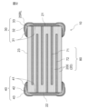
- FIG. 1(a) is a schematic perspective view of an electronic component according to Embodiment 1
- FIG. 1(b) is a schematic perspective view of a ceramic body used in the electronic component of FIG. 1(a).
- FIG. 2 is a schematic cross-sectional view of the electronic component taken along the line XX in FIG. 1(a).
- FIG. 3 is a schematic partially enlarged sectional view of the electronic component shown in FIG. 2.
- FIG. FIG. 4 is a schematic partially enlarged sectional view of the electronic component shown in FIG. 3.
- 5(a) is a microscopic photograph taken from the end surface side of the electronic component according to Embodiment 1
- FIG. 5(b) is an enlarged photograph of a part of FIG. 5(a).
- FIG. 6(a) to 6(f) are schematic cross-sectional views for explaining the process of forming a plating layer.
- FIG. 7(a) is a microscopic photograph of a cross section of an electronic component manufactured in an example
- FIG. 7(b) is a microscopic photograph of a cross section of an electronic component manufactured in a comparative example.
- FIG. 8 is an enlarged photograph of a part of the micrograph of FIG. 7(a).
- An electronic component includes a ceramic body and an external electrode provided on the surface of the ceramic body.
- the external electrode includes a base layer that covers the surface of the ceramic body and a plating layer that covers the base layer. Two mutually adjacent side surfaces and end surfaces of the ceramic body come into contact to form a corner of the ceramic body.
- the base layer of the external electrode covers a plurality of side surfaces including the end face and the two side surfaces of the ceramic body, except for the corners of the ceramic body. Part or all of the corners of the ceramic body may be exposed from the base layer.
- a plating layer is formed on the surface of such a base layer, the plating layer is difficult to be formed on the surface of the corner of the ceramic body, causing pinholes to be formed in the plating layer. Furthermore, since the bonding strength between the corners of the ceramic body and the plating layer is low, gaps are likely to form between them. If there are defects (pinholes, gaps, etc.) in the plating layer, there is a risk that the plating solution will penetrate into the inside of the plating layer. The plating solution that has entered may damage the ceramic body, which may reduce the reliability of electronic components.
- the thickness of the plating layer covering the corners of the ceramic body is made thicker than the thickness of the plating layer covering the center of the end face, thereby suppressing the occurrence of defects in the plating layer. It is something.
- the electronic component includes a ceramic body and external electrodes provided on the surface of the ceramic body, the shape, dimensions, and material of the ceramic body, as well as the number, arrangement, and shape of the external electrodes. etc. are not particularly limited. Internal electrodes may or may not be embedded inside the ceramic body. If an internal electrode is present, the internal electrode is electrically connected to the external electrode in a suitable manner.
- Electronic components to which the configuration of the embodiments of the present invention can be applied may be, for example, surface-mounted components, particularly chip components, and more specifically, capacitors such as multilayer ceramic capacitors, positive characteristic (or positive temperature coefficient), etc. , PTC) thermistor, negative characteristic (or negative temperature coefficient, NTC) thermistor, varistor, capacitor, etc.
- capacitors such as multilayer ceramic capacitors, positive characteristic (or positive temperature coefficient), etc. , PTC) thermistor, negative characteristic (or negative temperature coefficient, NTC) thermistor, varistor, capacitor, etc.
- PTC positive characteristic
- NTC negative temperature coefficient
- FIG. 1(a) is a schematic perspective view of an electronic component 10 according to Embodiment 1 of the present invention
- FIG. 1(b) is a ceramic element body 20 used in the electronic component 10 of FIG. 1(a).
- FIG. FIG. 2 is a schematic cross-sectional view of the electronic component 10 taken along the line XX in FIG. 1(a).
- 3 is a schematic partially enlarged sectional view of the electronic component 10 shown in FIG. 2
- FIG. 4 is a schematic partially enlarged sectional view of the electronic component 10 shown in FIG. 3, further enlarged.
- the electronic component 10 shown in FIGS. 1(a) and 2 is a multilayer ceramic capacitor.
- the electronic component 10 includes a ceramic body 20 and external electrodes 30 and 40 provided at the ends of the ceramic body 20.
- the external electrodes 30, 40 include base layers 31, 41 and plating layers 32, 42.
- the external electrodes 30, 40 can further include second plating layers 33, 43 that cover the plating layers 32, 42.
- the ceramic body 20 of the multilayer ceramic capacitor is composed of a plurality of ceramic layers 200 (see FIG. 2). Inside the ceramic body 20, internal electrodes 71 and 72 are provided. Internal electrodes 71 and 72 and ceramic layers 200 are alternately stacked to form a laminate 80. The internal electrodes 71 and 72 are exposed from either of the end faces 21 and 22 of the ceramic body 20 and are electrically connected to the external electrodes 30 and 40.
- the ceramic body 20 As shown in FIG. 1(b), the ceramic body 20 according to the first embodiment has a substantially rectangular parallelepiped shape, and includes two opposing end surfaces 21 and 22 and four side surfaces 23. Note that in FIG. 1(b), internal electrodes 71 and 72 exposed from end surfaces 21 and 22 are omitted for simplification of the drawing. Two mutually adjacent side surfaces 23 and an end surface (end surface 21 in FIG. 1(b)) of the ceramic body 20 are in contact to form a corner 25 (hatched area) of the ceramic body 20.
- the "corner 25 of the ceramic body 20" refers to a region that includes an apex 25t where two side surfaces 23 and an end face intersect, and a portion surrounding the apex 25t, and has a certain extent. (See Figure 1(b)).
- the corner portion 25 may be, for example, a range surrounded by an arc drawn on the side surface 23 and the end surface 21 with a radius r around the apex 25t.
- the dimension (radius r) of the corner portion 25 can be appropriately set according to the dimension of the electronic component 10. For example, in the case of the electronic component 10 of 0603 size, the dimension (radius r) of the corner 25 can be set to 1/5 of the width W of the electronic component 10 (that is, W/5).
- the corner 25 (more precisely, the ridgeline 25RL of the corner 25) is covered with the first plating region 321 of the plating layer 32. Therefore, a range surrounded by a circular arc drawn with the length 321R (FIG. 5(b)) of the first plating region 321 as the radius r may be defined as the corner 25 of the ceramic body 20.
- the base layer 31 of the external electrode 30 covers the side surfaces 23 and end surfaces 21 of the ceramic body 20 except for the corners 25 (FIG. 1(a)).
- the corner portion 25 of the ceramic body 20 may be completely exposed from the base layer 31 (that is, the corner portion 25 may not be covered by the base layer 31 at all).
- only a portion of the corner portion 25 may be exposed from the base layer 31, and the remaining portion may be covered with the base layer 31.
- the base layer 31 covering the corner 25 is extremely thin, the base layer 31 may not be able to form a continuous film (that is, a plurality of holes may be formed in the base layer 31, and the corner 25 may be formed from the hole). (a portion may be exposed).
- the thickness of the base layer 31 does not have to be uniform.
- the base layer 31 that covers the corners 25 of the ceramic body 20 or the vicinity thereof may be relatively thin, and the base layer 31 that covers the other portions may be relatively thick.
- the base layer 31 is provided for forming the plating layer 32 by electrolytic plating. Therefore, it is desirable that the thickness of the base layer 31 is sufficient for electrolytic plating and as thin as possible. Specifically, the thickness 31t of the base layer 31 is preferably 0.1 ⁇ m or more and 10 ⁇ m or less. By making the base layer 31 thinner, the thickness of the external electrode 30 (the total thickness of the base layer 31, the plating layer 32, and the second plating layer 33) can be made thinner. In addition, in this specification, “the thickness 31t of the base layer 31" refers to the maximum thickness of the base layer 31. The thickness 31t of the base layer 31 usually substantially matches the thickness of the plating layer covering the center 21c of the end surfaces 21 and 22 of the ceramic body 20.
- the plating layer 32 of the external electrode 30 covers the base layer 31 and the portion of the corner 25 of the ceramic body 20 exposed from the base layer 31.
- the plating layer 32 includes a plating layer (first plating region) 321 that covers the corner 25 of the ceramic body 20 and a plating layer (second plating region) 322 provided on the end surfaces 21 and 22 side of the ceramic body 20. , and a plating layer (third plating region) 323 provided on the side surface 23 side of the ceramic body 20.
- the thickness T1 of the plating layer 32 (first plating region 321) covering the corner 25 is greater than the thickness T2 of the plating layer 32 covering the center 21c of the end surface 21 (FIG. 1(b)). thick.
- defects pinholes in the plating layer 32, pinholes in the plating layer 32 and the ceramic body
- 20 can be suppressed from occurring.
- the thickness T1 of the first plating region 321 and the thickness T2 of the plating region 32 covering the center 21c of the end surface 21 of the ceramic body 20 are measured as follows. First, the electronic component 10 is cut along a cross section CS parallel to the LT plane (a cross section taken along line XX in FIG. 1(a)). The position of cross section CS is determined so that it passes through corner 25 and internal electrodes 71 and 72 arranged inside ceramic body 20 are exposed. Note that instead of cutting the electronic component 10 at the cross section CS, the electronic component 10 may be polished to the cross section CS.
- FIG. 3 illustrates a cross section of the electronic component 10 cut along the cross section SC.
- the ceramic body 20 shown in FIG. 3 includes a side surface 23, an end surface 21, and a ridgeline 25RL where these intersect.
- the ridge line 25RL will be explained with reference to FIG. 1(b).
- the ceramic body 20 has ridgelines 20RL1 and 20RL2 where the side surfaces 23 and end surfaces 21 are in contact, and a ridgeline 20RL3 where the two adjacent side surfaces 23 are in contact. Some of these ridgelines pass through the corner 25.
- the ridgeline within the range of the corner 25 is referred to as "the ridgeline 25RL of the corner 25.”
- the thickness T1 of the first plating region 321 covering the corner 25 is the thickness T1 from the ridgeline 25RL of the corner 25 of the ceramic body 20 to the outer surface of the first plating region 321 in a cross-sectional view of the electronic component 10 (FIG. 3). It is distance. Note that the edges of the ridgeline 25RL of the corner portion 25 may be removed during manufacturing, resulting in a curved surface (drawn as a curved line in FIG. 3).
- the thickness T2 of the plating layer 32 covering the center 21c of the end surface 21 of the ceramic body 20 needs to be measured on a cross section of the electronic component 10 cut along a plane passing through the center 21c of the end surface 21.
- the second plating region 322 shown in FIG. 3 and the plating layer 32 covering the center 21c of the end surface 21 have approximately the same thickness. Therefore, the thickness of the second plating region 322 in the cross-sectional view of FIG. 3 is regarded as the thickness of the plating layer 32 covering the center 21c of the end surface 21.
- the thickness of the plating layer 32 covering the center 21c of the end surface 21 may be referred to as the thickness T2 of the second plating region 322.
- the thickness T1 of the first plating region 321 covering the corner 25 is 1.5 times or more the thickness T2 of the plating layer 32 covering the center 21c of the end face 21 (that is, the thickness of the second plating region 322). It is preferable. Thereby, the thickness T1 of the first plating layer 321 covering the corner portion 25 becomes sufficiently thick, and the suppressing effect of suppressing the penetration of the plating solution into the inside of the plating layer 32 is further improved. More preferably, the thickness T1 of the first plating region 321 is twice or more the thickness T2 of the second plating region 322, and even more preferably three times or more and six times or less.
- the first plating region 321 covering the corner 25 is preferably made of a laminated film in which a plurality of plating films are laminated.
- the first plating region 321 is composed of three plating films 321a, 321b, and 321c.
- the laminated film preferably has two to ten plating films, more preferably two to four plating films.
- the number of plating film layers constituting the first plating region 321 is calculated as (number of cracks CL)+1.
- the plating film is counted as "three layers”.
- the crack CL can be confirmed by observing the cross section of the first plating region 321 with a microscope (microscope or optical microscope) (FIG. 7(a), FIG. 8).
- the first plating region 321 is observed with a microscope at a magnification of 100 times or more, and if a gap with a width of 1 ⁇ m or more is continuous for 1 ⁇ m or more, it is determined to be a “crack CL”.
- FIG. 5(a) is a microscopic photograph taken from the end surface 21 side of the electronic component 10 according to Example 1, which will be described later, and FIG. 5(b) is a microscopic photograph enlarging a part of FIG. 5(a).
- the dimension of the first plating region 321 along the ridgeline 20RL1 of the ceramic body 20 is defined as "length 321R.”
- the length 321R of the first plating region 321 is, for example, 0.1 ⁇ m or more and 100 ⁇ m or less.
- the length 321R of the first plating region 321 is more preferably 20 ⁇ m or more and 60 ⁇ m or less.
- the length 321R of the first plating region 321 is measured as follows.
- a side surface 23 of the ceramic body 20, an end surface 21 of the ceramic body 20, and ridge lines 20RL1 and 20RL2 of the ceramic body 20 are drawn.
- the side surface 23 and the end surface 21 are in contact with each other at the ridge line 20RL1 or the ridge line 20RL2 of the ceramic body 20 (see also FIG. 1(b)).
- the plating layer 32 (first plating region 321) covering the corner 25 of the ceramic body 20 covers the apex 25t of the corner 25 of the ceramic body 20, Furthermore, it extends along each of the ridge lines 20RL1 and 20RL2 of the ceramic body 20.
- the first plating region 321 has an L-shape.
- the ceramic body 20 has a ridgeline 20RL3 where two mutually adjacent side surfaces 23 touch (see FIG. 1(b)).
- the first plating region 321 further covers the apex 25t of the corner 25 of the ceramic body 20 and extends along the ridge line 20RL3 of the ceramic body 20.
- the length 321R of the first plating region 321 along the ridgeline 20RL1 of the ceramic body 20 is approximately equal to the length of the first plating region 321 measured along each of the other ridgelines 20RL2 and 20RL3. Therefore, when measuring the length of the first plating region 321, it may be measured along any of the ridgelines.
- the first plating region 321 and the second plating region 322 have different thicknesses and surface properties, so when observed with a microscope (microscope or optical microscope) , those areas appear to have different tones. Therefore, the range of the first plating region 321 can be specified based on the color tone. After specifying the range of the first plating region 321, the length of the first plating region 321 is measured.
- the base layers 31 and 41 can be made thinner without producing defects (pinholes, gaps, etc.) in the plating layers 32 and 42. Therefore, for the following reasons, it is particularly suitable for an electronic component 10 including internal electrodes 71 and 72 inside a ceramic body 20, such as a multilayer ceramic capacitor shown in FIG.
- the thickness of the external electrodes 30, 40 can be reduced by making the base layers 31, 41 thinner. Therefore, the number of internal electrodes 71 and 72 can be increased without changing the external dimensions of electronic component 10. Thereby, the capacitance of the multilayer ceramic capacitor can be improved. Even in other electronic components including internal electrodes (such as multilayer thermistors), the number of internal electrodes can be increased, so the electrical characteristics of the electronic component can be improved.
- Method for manufacturing electronic component 10 A method for manufacturing the electronic component 10 according to the first embodiment will be explained using a multilayer ceramic capacitor having the structure shown in FIG. 2 as an example.
- Ceramic body 20 (Production of ceramic body 20 and internal electrodes 71 and 72) First, a ceramic body 20 containing internal electrodes 71 and 72 is prepared. Ceramic body 20 can be produced by any suitable method.
- the ceramic body 20 (more specifically, the ceramic layer 200) is formed from a ceramic material suitable for the electronic component to be manufactured.
- the ceramic body 20 is made of a dielectric ceramic material (for example, BaTiO 3 , CaTiO 3 , SrTiO 3 , CaZrO 3 , (BaSr)TiO 3 , Ba(ZrTi)O 3 , (BiZn)Nb 2 O 7 etc.).
- the internal electrodes 71 and 72 are formed from a conductive material. Suitable conductive materials are, for example, Ag, Cu, Pt, Ni, Al, Pd, Au, etc., with Ag, Cu, and Ni being particularly preferred.
- each raw material of the ceramic body 20 is weighed, and a grinding medium such as partially stabilized zirconia (PSZ) (hereinafter also referred to as PSZ balls) is used. and pure water into a ball mill for wet mixing and pulverization.
- PSZ partially stabilized zirconia
- the obtained mixture is calcined at a predetermined temperature (for example, 1000 to 1200°C) to obtain calcined powder.
- An organic binder is added to the obtained calcined powder, wet-mixed to form a slurry, and then shaped using a doctor blade method or the like to produce a ceramic green sheet of a desired thickness.
- a conductive paste for forming the internal electrodes 71 and 72 is applied to the surface of the ceramic green sheet to form an internal electrode pattern.
- a conductive paste is prepared, for example, by dispersing metal powder and an organic binder in an organic solvent.
- the conductive paste is applied by, for example, screen printing.
- base layers 31 and 41 are applied so as to cover the ends of the ceramic body 20 (as shown in FIG. Form.
- the base layers 31 and 41 are in contact with internal electrodes 71 and 72 exposed on the end surfaces 21 and 22 of the ceramic body 20.
- the base layers 31 and 41 are formed from a metal material containing, for example, Cu, Ag, Si, Ni, or the like. In particular, it is preferable to form it from a Cu film.
- the base layers 31 and 41 can be formed by a known film forming method. For example, a sputtering method, a vapor deposition method, a coating method (conductive paste is applied to a predetermined position and then baked), a dipping method, etc. can be used. For example, for the Cu film, it is preferable to apply a Cu paste and then bake it. By forming the Cu film thinly, the corners 25 of the ceramic body 20 are at least partially exposed from the base layers 31 and 41.
- Plating layers 32 and 42 are formed to cover the base layers 31 and 41 and the portions of the corners 25 of the ceramic body 20 exposed from the base layer 31.
- the plating layers 32 and 42 can be formed, for example, by electrolytically plating at least one of Ni and Cu.
- the plating layers 32 and 42 can be formed, for example, by a barrel plating method in which conductive media placed in a barrel and the ceramic body 20 are plated while being rotated and agitated, or by agitating the ceramic body 20 by the centrifugal force of the barrel.
- a plating method that applies impact to the object to be plated such as centrifugal plating.
- the plating layer 32 (first plating region 321) covering the corner portion 25 of the ceramic body 20 can be formed into a thick film.
- a plating layer 32a is formed on the surface of the base layers 31 and 41 by centrifugal plating. .
- the plating layer 32a is first formed on the surfaces of the base layers 31 and 41, and spreads over time to the surface of the corner 25 of the ceramic body 20 (FIG. 6(b)).
- the plating layer 32a covering the corner 25 of the ceramic body 20 has a weak bonding force with the surface of the corner 25.
- collisions between the ceramic bodies 20, between the ceramic bodies 20 and the conductive media, and between the ceramic bodies 20 and the cathode cause the ceramic bodies 20 to collide with the cathode due to centrifugal force.
- the plating layer 32a is easily peeled off from the surface of the corner portion 25 due to the friction generated when it sticks to the corner portion 25 (FIG. 6(c)). As a result, the corner portion 25 is exposed from the plating layer 32a. Note that since the bond between the plating layer 32a and the base layers 31 and 41 is strong, the plating layer 32a is only partially peeled off.
- Plating is continued with a portion of the plating layer 32a peeled off.
- a plating layer 32b covering the surface of the corner 25 is formed again using the base layers 31, 41 and/or the previously formed plating layer 32a (FIG. 6(d)).
- the thickness of the plating layer 32a formed earlier increases.
- the plating grows on both the inside (the surface that was in contact with the surface of the corner 25 before peeling) and the outside.
- the plating layer 32b covering the corner 25 is easily removed from the surface of the corner 25 by various collisions and frictions (as described above) that the ceramic body 20 may receive during centrifugal plating. It peels off (Fig. 6(e)).
- the plating layer 32c covering the surface of the corner 25 is formed again, starting from the base layers 31, 41 and/or the previously formed plating layers 32a, 32b. (FIG. 6(f)).
- the thickness of the plating layers 32a and 32b formed earlier increases. In particular, plating grows on both the inside and outside of the peeled portions of the plating layers 32a and 32b.
- the plating layer 32 (first plating area 321) covering the corner 25 is removed from the other plating layer 32 (second plating area). 322 and third plating region 323).
- the thickness T1 of the first plating region 321 can be adjusted by adjusting the length of plating time. By lengthening the plating time, the thickness T1 of the first plating region 321 can be increased.
- the number of layers of plating films 321a, 321b, and 321c forming the first plating region 321 is determined by the number of times of peeling. Adjustment of the strength of the impact that the ceramic body 20 (more precisely, the plating film formed on the surface of the ceramic body 20) receives during centrifugal plating (for example, the rotation speed of the container (barrel) in which the chips and media are placed)
- the number of layers of the plating films 321a, 321b, and 321c can be controlled by controlling the number of times of peeling by adjusting the plating time.
- the plating time is preferably in the range of 30 minutes to 600 minutes, and the rotation speed is preferably in the range of 200 to 500 rpm.
- Second plating layers 33 and 43 are formed to cover the surfaces of plating layers 32 and 42.
- the second plating layers 33 and 43 can be formed, for example, by electroplating Sn.
- the second plating layers 33 and 43 can be formed by a known plating method, for example, a barrel plating method, a centrifugal plating method, or the like.
- a measurement sample was prepared according to the following procedure.
- the ceramic body 20 was prepared by pulverizing and mixing raw materials, calcination, molding, firing, and cutting.
- the pulverization and mixing of the raw materials involved mixing a predetermined amount of BaTiO 3 as the main component, pulverizing the mixture, and pre-calcining the mixture at a maximum temperature of 1200° C. in an air atmosphere.
- An organic binder was added to the obtained calcined powder and wet mixed to obtain a slurry.
- a ceramic green sheet with a desired thickness was produced from the slurry by the doctor blade method.
- a conductive paste for internal electrodes (Ag paste) was applied to the surface of the ceramic green sheet to form an internal electrode pattern.
- a laminate was produced by stacking a predetermined number of ceramic green sheets on which internal electrode patterns were formed in this way, and then sandwiching and pressing the top and bottom with ceramic green sheets on which no internal electrode patterns were formed. After cutting this laminate into predetermined dimensions, it is subjected to degreasing and binder removal treatments, and then fired at a predetermined temperature (1200 to 1400°C) and in a predetermined atmosphere to separate the ceramic body 20 and internal electrodes 71 and 72. A laminate 80 having a laminate structure was obtained.
- a base layer 31 was formed by applying Cu paste to the end of the ceramic body 20 and baking it. At this time, the corner portion 25 of the ceramic body 20 was exposed from the base layer 31 (FIG. 7(a), FIG. 8).
- a plating layer 32 Ni plating layer covering the surface of the base layer 31 and the corners 25 of the ceramic body 20 was formed by centrifugal plating. When performing centrifugal plating, the number of rotations of the barrel (container that holds the chips and media) was increased and the plating time was increased compared to typical centrifugal plating conditions. As a result, the Ni plating layer was laminated on the corner portion 25 of the ceramic body 20 that is susceptible to impact.
- a second plating layer 33 (Sn plating layer) covering the Ni plating layer was formed by centrifugal plating.
- the plating conditions were general plating conditions. In this way, a multilayer ceramic capacitor was obtained (sample of Example 1).
- the sample was filled with resin and polished to the line XX in FIG. 1(a) to expose the cross section SC (parallel to the LT plane), followed by ion milling.
- the first plating regions 321 of the external electrodes 30 and 40 were observed using a microscope (Keyence: VHX7000). Microscopic photographs of the sample of Example 1 are shown in FIGS. 7(a) and 8.
- the first plating region 321 covering the corner 25 of the ceramic body 20 was a laminated film of three Ni plating films 321a, 321b, and 321c (FIG. 8). Furthermore, no pinholes were present in the Ni plating layer 32.
- the length 321R (FIG. 5(b)) of the first plating region 321 was measured, it was approximately 55 ⁇ m.
- Comparative Example 1 A sample of Comparative Example 1 was produced in the same steps as Example 1 except for the conditions for forming the plating layer 32 (Ni plating layer).
- the Ni plating layer 32 was plated under general centrifugal plating conditions. Thereby, the impact applied to the corner portion 25 of the ceramic body 20 was reduced, and the stacking of the Ni plating layer 32 was suppressed.
- Example 1 10,000 samples of Example 1 and 10,000 samples of Comparative Example 1 were each produced, and the following evaluations were performed.
- - Number of plating solution penetrated The number of samples in which the plating solution penetrated inside the Ni plating layer was counted.
- IR Insulation Resistance
- the insulation resistance value is measured after a certain period of time (24 hours or more) has passed in a high temperature (70°C or higher) and high humidity (50% or higher) environment to confirm whether the initial insulation resistance value can be maintained. did.
- the measured insulation resistance value exceeded 90% of the initial insulation resistance value, it was judged as OK (good product), and when it was 90% or less, it was judged as NG (defective product).
- Example 1 As shown in Table 1, in Comparative Example 1, penetration of the plating solution was confirmed in 521 out of 10,000 samples. On the other hand, in Example 1, out of 10,000 samples, there were no samples in which penetration of the plating solution was confirmed. Regarding reliability evaluation, in Comparative Example 1, 26 out of 10,000 samples were defective. In Example 1, there were no defective products among 10,000 samples.
Landscapes
- Engineering & Computer Science (AREA)
- Power Engineering (AREA)
- Manufacturing & Machinery (AREA)
- Microelectronics & Electronic Packaging (AREA)
- Chemical & Material Sciences (AREA)
- Ceramic Engineering (AREA)
- Inorganic Chemistry (AREA)
- Ceramic Capacitors (AREA)
- Fixed Capacitors And Capacitor Manufacturing Machines (AREA)
Priority Applications (4)
| Application Number | Priority Date | Filing Date | Title |
|---|---|---|---|
| JP2024506054A JP7619521B2 (ja) | 2022-03-10 | 2023-02-22 | 電子部品 |
| KR1020247030450A KR102930444B1 (ko) | 2022-03-10 | 2023-02-22 | 전자부품 |
| CN202380024390.3A CN118805231A (zh) | 2022-03-10 | 2023-02-22 | 电子部件 |
| US18/828,159 US20240428995A1 (en) | 2022-03-10 | 2024-09-09 | Electronic component |
Applications Claiming Priority (2)
| Application Number | Priority Date | Filing Date | Title |
|---|---|---|---|
| JP2022-037424 | 2022-03-10 | ||
| JP2022037424 | 2022-03-10 |
Related Child Applications (1)
| Application Number | Title | Priority Date | Filing Date |
|---|---|---|---|
| US18/828,159 Continuation US20240428995A1 (en) | 2022-03-10 | 2024-09-09 | Electronic component |
Publications (1)
| Publication Number | Publication Date |
|---|---|
| WO2023171394A1 true WO2023171394A1 (ja) | 2023-09-14 |
Family
ID=87934971
Family Applications (1)
| Application Number | Title | Priority Date | Filing Date |
|---|---|---|---|
| PCT/JP2023/006550 Ceased WO2023171394A1 (ja) | 2022-03-10 | 2023-02-22 | 電子部品 |
Country Status (5)
| Country | Link |
|---|---|
| US (1) | US20240428995A1 (https=) |
| JP (1) | JP7619521B2 (https=) |
| KR (1) | KR102930444B1 (https=) |
| CN (1) | CN118805231A (https=) |
| WO (1) | WO2023171394A1 (https=) |
Citations (5)
| Publication number | Priority date | Publication date | Assignee | Title |
|---|---|---|---|---|
| JP2008300769A (ja) * | 2007-06-04 | 2008-12-11 | Murata Mfg Co Ltd | セラミック電子部品及びその製造方法 |
| JP2015111655A (ja) * | 2013-10-29 | 2015-06-18 | 株式会社村田製作所 | セラミック電子部品 |
| JP2019062100A (ja) * | 2017-09-27 | 2019-04-18 | 太陽誘電株式会社 | セラミック電子部品およびその製造方法 |
| JP2019149410A (ja) * | 2018-02-26 | 2019-09-05 | 京セラ株式会社 | 電子部品 |
| JP2021190546A (ja) * | 2020-05-29 | 2021-12-13 | 株式会社村田製作所 | 積層セラミックコンデンサ |
Family Cites Families (2)
| Publication number | Priority date | Publication date | Assignee | Title |
|---|---|---|---|---|
| JP2012069912A (ja) | 2010-08-27 | 2012-04-05 | Tdk Corp | 電子部品の製造方法及び電子部品 |
| JP6060945B2 (ja) | 2014-07-28 | 2017-01-18 | 株式会社村田製作所 | セラミック電子部品およびその製造方法 |
-
2023
- 2023-02-22 KR KR1020247030450A patent/KR102930444B1/ko active Active
- 2023-02-22 CN CN202380024390.3A patent/CN118805231A/zh active Pending
- 2023-02-22 WO PCT/JP2023/006550 patent/WO2023171394A1/ja not_active Ceased
- 2023-02-22 JP JP2024506054A patent/JP7619521B2/ja active Active
-
2024
- 2024-09-09 US US18/828,159 patent/US20240428995A1/en active Pending
Patent Citations (5)
| Publication number | Priority date | Publication date | Assignee | Title |
|---|---|---|---|---|
| JP2008300769A (ja) * | 2007-06-04 | 2008-12-11 | Murata Mfg Co Ltd | セラミック電子部品及びその製造方法 |
| JP2015111655A (ja) * | 2013-10-29 | 2015-06-18 | 株式会社村田製作所 | セラミック電子部品 |
| JP2019062100A (ja) * | 2017-09-27 | 2019-04-18 | 太陽誘電株式会社 | セラミック電子部品およびその製造方法 |
| JP2019149410A (ja) * | 2018-02-26 | 2019-09-05 | 京セラ株式会社 | 電子部品 |
| JP2021190546A (ja) * | 2020-05-29 | 2021-12-13 | 株式会社村田製作所 | 積層セラミックコンデンサ |
Also Published As
| Publication number | Publication date |
|---|---|
| KR20240149943A (ko) | 2024-10-15 |
| JP7619521B2 (ja) | 2025-01-22 |
| JPWO2023171394A1 (https=) | 2023-09-14 |
| CN118805231A (zh) | 2024-10-18 |
| US20240428995A1 (en) | 2024-12-26 |
| KR102930444B1 (ko) | 2026-02-25 |
Similar Documents
| Publication | Publication Date | Title |
|---|---|---|
| JP7274372B2 (ja) | セラミック電子部品およびその製造方法 | |
| JP7125093B2 (ja) | 積層セラミックコンデンサ及びその製造方法 | |
| US10734159B2 (en) | Multilayer ceramic capacitor and method for manufacturing multilayer ceramic capacitor | |
| JP7167227B2 (ja) | 積層セラミックコンデンサ | |
| JP2024101063A (ja) | 積層セラミック電子部品 | |
| JP2022133553A (ja) | 積層セラミックコンデンサ | |
| KR20190046650A (ko) | 적층 세라믹 콘덴서 및 적층 세라믹 콘덴서의 제조 방법 | |
| JP7665343B2 (ja) | セラミック電子部品およびその製造方法 | |
| JP2019033243A (ja) | 積層セラミックコンデンサおよびその製造方法 | |
| JP2017028254A (ja) | 積層セラミックコンデンサ | |
| KR20180113457A (ko) | 적층 세라믹 콘덴서 | |
| JP2022119088A (ja) | セラミック電子部品およびその製造方法 | |
| JP2001220224A (ja) | 誘電体磁器と積層セラミック電子部品 | |
| JP2020119965A (ja) | 積層セラミックコンデンサ及び積層セラミックコンデンサの製造方法 | |
| JP2021052103A (ja) | セラミック電子部品の製造方法及びセラミック電子部品 | |
| JP6935707B2 (ja) | 積層セラミックコンデンサ | |
| JP7493322B2 (ja) | 積層セラミックコンデンサ | |
| JP7209072B2 (ja) | 積層セラミックコンデンサ | |
| KR102902806B1 (ko) | 세라믹 전자 부품 및 그 제조 방법, 그리고 회로 기판 | |
| JP7619521B2 (ja) | 電子部品 | |
| JP7556469B2 (ja) | 電子部品 | |
| KR20200067807A (ko) | 적층 세라믹 커패시터 | |
| JP2021005673A (ja) | 積層セラミックコンデンサ及びその製造方法 | |
| US20240331943A1 (en) | Electronic component and method for producing electronic component | |
| JP2026048921A (ja) | 積層セラミック電子部品及び積層セラミック電子部品の製造方法 |
Legal Events
| Date | Code | Title | Description |
|---|---|---|---|
| 121 | Ep: the epo has been informed by wipo that ep was designated in this application |
Ref document number: 23766572 Country of ref document: EP Kind code of ref document: A1 |
|
| ENP | Entry into the national phase |
Ref document number: 2024506054 Country of ref document: JP Kind code of ref document: A |
|
| WWE | Wipo information: entry into national phase |
Ref document number: 202380024390.3 Country of ref document: CN |
|
| ENP | Entry into the national phase |
Ref document number: 20247030450 Country of ref document: KR Kind code of ref document: A |
|
| WWE | Wipo information: entry into national phase |
Ref document number: 1020247030450 Country of ref document: KR |
|
| NENP | Non-entry into the national phase |
Ref country code: DE |
|
| 122 | Ep: pct application non-entry in european phase |
Ref document number: 23766572 Country of ref document: EP Kind code of ref document: A1 |
|
| WWG | Wipo information: grant in national office |
Ref document number: 1020247030450 Country of ref document: KR |