WO2023032774A1 - 複合電子部品 - Google Patents
複合電子部品 Download PDFInfo
- Publication number
- WO2023032774A1 WO2023032774A1 PCT/JP2022/031824 JP2022031824W WO2023032774A1 WO 2023032774 A1 WO2023032774 A1 WO 2023032774A1 JP 2022031824 W JP2022031824 W JP 2022031824W WO 2023032774 A1 WO2023032774 A1 WO 2023032774A1
- Authority
- WO
- WIPO (PCT)
- Prior art keywords
- electronic component
- circuit layer
- ceramic
- ceramic electronic
- composite
- Prior art date
- Legal status (The legal status is an assumption and is not a legal conclusion. Google has not performed a legal analysis and makes no representation as to the accuracy of the status listed.)
- Ceased
Links
Images


Classifications
-
- H—ELECTRICITY
- H01—ELECTRIC ELEMENTS
- H01G—CAPACITORS; CAPACITORS, RECTIFIERS, DETECTORS, SWITCHING DEVICES, LIGHT-SENSITIVE OR TEMPERATURE-SENSITIVE DEVICES OF THE ELECTROLYTIC TYPE
- H01G4/00—Fixed capacitors; Processes of their manufacture
- H01G4/002—Details
- H01G4/018—Dielectrics
- H01G4/06—Solid dielectrics
- H01G4/08—Inorganic dielectrics
- H01G4/12—Ceramic dielectrics
- H01G4/1209—Ceramic dielectrics characterised by the ceramic dielectric material
- H01G4/1218—Ceramic dielectrics characterised by the ceramic dielectric material based on titanium oxides or titanates
- H01G4/1227—Ceramic dielectrics characterised by the ceramic dielectric material based on titanium oxides or titanates based on alkaline earth titanates
-
- H—ELECTRICITY
- H01—ELECTRIC ELEMENTS
- H01G—CAPACITORS; CAPACITORS, RECTIFIERS, DETECTORS, SWITCHING DEVICES, LIGHT-SENSITIVE OR TEMPERATURE-SENSITIVE DEVICES OF THE ELECTROLYTIC TYPE
- H01G4/00—Fixed capacitors; Processes of their manufacture
- H01G4/002—Details
- H01G4/228—Terminals
- H01G4/232—Terminals electrically connecting two or more layers of a stacked or rolled capacitor
-
- H—ELECTRICITY
- H01—ELECTRIC ELEMENTS
- H01G—CAPACITORS; CAPACITORS, RECTIFIERS, DETECTORS, SWITCHING DEVICES, LIGHT-SENSITIVE OR TEMPERATURE-SENSITIVE DEVICES OF THE ELECTROLYTIC TYPE
- H01G4/00—Fixed capacitors; Processes of their manufacture
- H01G4/30—Stacked capacitors
-
- H—ELECTRICITY
- H01—ELECTRIC ELEMENTS
- H01G—CAPACITORS; CAPACITORS, RECTIFIERS, DETECTORS, SWITCHING DEVICES, LIGHT-SENSITIVE OR TEMPERATURE-SENSITIVE DEVICES OF THE ELECTROLYTIC TYPE
- H01G4/00—Fixed capacitors; Processes of their manufacture
- H01G4/40—Structural combinations of fixed capacitors with other electric elements, the structure mainly consisting of a capacitor, e.g. RC combinations
-
- H—ELECTRICITY
- H05—ELECTRIC TECHNIQUES NOT OTHERWISE PROVIDED FOR
- H05K—PRINTED CIRCUITS; CASINGS OR CONSTRUCTIONAL DETAILS OF ELECTRIC APPARATUS; MANUFACTURE OF ASSEMBLAGES OF ELECTRICAL COMPONENTS
- H05K3/00—Apparatus or processes for manufacturing printed circuits
- H05K3/46—Manufacturing multilayer circuits
-
- H—ELECTRICITY
- H10—SEMICONDUCTOR DEVICES; ELECTRIC SOLID-STATE DEVICES NOT OTHERWISE PROVIDED FOR
- H10W—GENERIC PACKAGES, INTERCONNECTIONS, CONNECTORS OR OTHER CONSTRUCTIONAL DETAILS OF DEVICES COVERED BY CLASS H10
- H10W20/00—Interconnections in chips, wafers or substrates
- H10W20/40—Interconnections external to wafers or substrates, e.g. back-end-of-line [BEOL] metallisations or vias connecting to gate electrodes
- H10W20/41—Interconnections external to wafers or substrates, e.g. back-end-of-line [BEOL] metallisations or vias connecting to gate electrodes characterised by their conductive parts
- H10W20/43—Layouts of interconnections
-
- H—ELECTRICITY
- H10—SEMICONDUCTOR DEVICES; ELECTRIC SOLID-STATE DEVICES NOT OTHERWISE PROVIDED FOR
- H10W—GENERIC PACKAGES, INTERCONNECTIONS, CONNECTORS OR OTHER CONSTRUCTIONAL DETAILS OF DEVICES COVERED BY CLASS H10
- H10W44/00—Electrical arrangements for controlling or matching impedance
- H10W44/601—Capacitive arrangements
-
- H—ELECTRICITY
- H10—SEMICONDUCTOR DEVICES; ELECTRIC SOLID-STATE DEVICES NOT OTHERWISE PROVIDED FOR
- H10W—GENERIC PACKAGES, INTERCONNECTIONS, CONNECTORS OR OTHER CONSTRUCTIONAL DETAILS OF DEVICES COVERED BY CLASS H10
- H10W70/00—Package substrates; Interposers; Redistribution layers [RDL]
- H10W70/60—Insulating or insulated package substrates; Interposers; Redistribution layers
- H10W70/611—Insulating or insulated package substrates; Interposers; Redistribution layers for connecting multiple chips together
-
- H—ELECTRICITY
- H10—SEMICONDUCTOR DEVICES; ELECTRIC SOLID-STATE DEVICES NOT OTHERWISE PROVIDED FOR
- H10W—GENERIC PACKAGES, INTERCONNECTIONS, CONNECTORS OR OTHER CONSTRUCTIONAL DETAILS OF DEVICES COVERED BY CLASS H10
- H10W70/00—Package substrates; Interposers; Redistribution layers [RDL]
- H10W70/60—Insulating or insulated package substrates; Interposers; Redistribution layers
- H10W70/62—Insulating or insulated package substrates; Interposers; Redistribution layers characterised by their interconnections
- H10W70/63—Vias, e.g. via plugs
- H10W70/635—Through-vias
-
- H—ELECTRICITY
- H10—SEMICONDUCTOR DEVICES; ELECTRIC SOLID-STATE DEVICES NOT OTHERWISE PROVIDED FOR
- H10W—GENERIC PACKAGES, INTERCONNECTIONS, CONNECTORS OR OTHER CONSTRUCTIONAL DETAILS OF DEVICES COVERED BY CLASS H10
- H10W70/00—Package substrates; Interposers; Redistribution layers [RDL]
- H10W70/60—Insulating or insulated package substrates; Interposers; Redistribution layers
- H10W70/67—Insulating or insulated package substrates; Interposers; Redistribution layers characterised by their insulating layers or insulating parts
- H10W70/69—Insulating materials thereof
- H10W70/692—Ceramics or glasses
-
- H—ELECTRICITY
- H10—SEMICONDUCTOR DEVICES; ELECTRIC SOLID-STATE DEVICES NOT OTHERWISE PROVIDED FOR
- H10W—GENERIC PACKAGES, INTERCONNECTIONS, CONNECTORS OR OTHER CONSTRUCTIONAL DETAILS OF DEVICES COVERED BY CLASS H10
- H10W90/00—Package configurations
-
- H—ELECTRICITY
- H10—SEMICONDUCTOR DEVICES; ELECTRIC SOLID-STATE DEVICES NOT OTHERWISE PROVIDED FOR
- H10W—GENERIC PACKAGES, INTERCONNECTIONS, CONNECTORS OR OTHER CONSTRUCTIONAL DETAILS OF DEVICES COVERED BY CLASS H10
- H10W70/00—Package substrates; Interposers; Redistribution layers [RDL]
- H10W70/60—Insulating or insulated package substrates; Interposers; Redistribution layers
- H10W70/611—Insulating or insulated package substrates; Interposers; Redistribution layers for connecting multiple chips together
- H10W70/614—Insulating or insulated package substrates; Interposers; Redistribution layers for connecting multiple chips together the multiple chips being integrally enclosed
Definitions
- the present invention relates to a composite electronic component in which multiple circuit layers are laminated.
- Composite electronic components are known, in which multiple circuit layers including electronic components and wiring are laminated.
- Patent Document 1 discloses a first semiconductor package (first circuit layer) 201 and a second semiconductor package (second circuit layer) as shown in FIG.
- a package-on-package device 200 is disclosed in which three semiconductor packages are stacked, 202 and a third semiconductor package (third circuit layer) 203 .
- Each of the semiconductor packages 201 , 202 , 203 has a structure in which a semiconductor chip 220 is mounted on a package substrate 210 and the periphery of the semiconductor chip 220 is covered with a resin 230 .
- An object of the present invention is to solve the above problems, and to provide a composite electronic component capable of reducing connection resistance between a plurality of laminated circuit layers.
- the composite electronic component of the present invention is a composite electronic component in which a plurality of circuit layers containing electronic components are laminated, a first circuit layer; a second circuit layer; A plurality of via electrodes are disposed between the first circuit layer and the second circuit layer and are exposed on one main surface and the other main surface through a main body whose main component is ceramic.
- a ceramic electronic component comprising; a sealing resin covering at least the ceramic electronic component between the first circuit layer and the second circuit layer; with At least one electronic component included in the first circuit layer and at least one electronic component included in the second circuit layer are electrically connected by the via electrodes of the ceramic electronic component. It is characterized by
- a plurality of via electrodes are provided between the first circuit layer and the second circuit layer, penetrating through the main body and exposed to one main surface and the other main surface, respectively. and a via electrode of the ceramic electronic component is provided between at least one electronic component included in the first circuit layer and at least one electronic component included in the second circuit layer. electrically connected. That is, since electrical connection is made by via electrodes of the ceramic electronic component without using solder bumps, the connection resistance can be reduced.
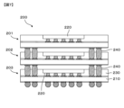
- FIG. 1 is a cross-sectional view showing a schematic configuration of a composite electronic component in one embodiment
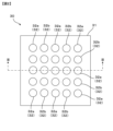
- FIG. 1 is a plan view schematically showing the configuration of a ceramic electronic component
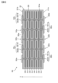
- FIG. 3 is a cross-sectional view of the ceramic electronic component shown in FIG. 2 taken along line III-III
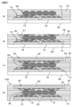
- (a) to (e) are diagrams for explaining an example of a method for manufacturing a composite electronic component according to an embodiment
- 4(a) to 4(d) are diagrams for explaining an example of the manufacturing method of the composite electronic component according to the embodiment, following FIG. 4(e);
- FIG. 4 is a diagram showing the results of a simulation of the degree of deformation when the composite electronic component was cooled from 150° C.
- FIG. 1 shows a cross-sectional view schematically showing the configuration of a package-on-package device described in Patent Document 1;
- the composite electronic component of the present invention has a structure in which a plurality of circuit layers containing electronic components are laminated.
- FIG. 1 is a cross-sectional view showing a schematic configuration of a composite electronic component 100 according to one embodiment.
- the composite electronic component 100 in one embodiment includes a first circuit layer 10, a second circuit layer 20, and a ceramic electronic component 30 disposed between the first circuit layer 10 and the second circuit layer 20. and a sealing resin 40 covering at least the ceramic electronic component 30 between the first circuit layer 10 and the second circuit layer 20 . That is, the composite electronic component 100 in this embodiment has a three-layer structure in which the first circuit layer 10, the ceramic electronic component 30, and the second circuit layer 20 are laminated in order.
- the first circuit layer 10 and the second circuit layer 20 each include wiring and electronic components.
- the first circuit layer 10 includes a first wiring 11 and a first electronic component 12 .
- the second circuit layer 20 also includes a second wiring 21 and a second electronic component 22 .
- two first electronic components 12 are shown in FIG. 1, the number of first electronic components 12 included in the first circuit layer 10 is not particularly limited.
- one second electronic component 22 is shown in FIG. 1, the number of second electronic components 22 included in the second circuit layer 20 is not particularly limited.
- the first circuit layer 10 contains the first insulating resin 13 .
- the first insulating resin 13 is located between the first electronic component 12 and the ceramic electronic component 30 .
- the first insulating resin 13 is an insulating resin such as polyimide resin.
- the thickness of the first insulating resin 13 is, for example, 5 ⁇ m.
- the second circuit layer 20 contains the second insulating resin 23 .
- a second insulating resin 23 is located between the second electronic component 22 and the ceramic electronic component 30 .
- the second insulating resin 23 is a resin having insulating properties, such as a polyimide resin.
- the thickness of the second insulating resin 23 is, for example, 5 ⁇ m.
- the first wiring 11 is wiring for electrically connecting the first electronic component 12 and the ceramic electronic component 30 and is provided inside the first insulating resin 13 . However, part of the first wirings 11 may be provided on the surface of the first insulating resin 13 .
- the first wiring 11 may be made of any material as long as it has conductivity, such as Cu.
- the second wiring 21 is wiring for electrically connecting the second electronic component 22 and the ceramic electronic component 30 and is provided inside the second insulating resin 23 . However, part of the second wirings 21 may be provided on the surface of the second insulating resin 23 .
- the material of the second wiring 21 may be any material as long as it has conductivity, such as Cu.
- the first circuit layer 10 includes a plurality of first electronic components 12
- the first circuit layer 10 includes wiring that electrically connects the first electronic components 12 to each other.
- the second circuit layer 20 includes a plurality of second electronic components 22
- the second circuit layer 20 includes wiring that electrically connects the second electronic components 22 to each other.
- the first electronic component 12 and the second electronic component 22 are, for example, semiconductor devices such as logic ICs such as CPUs and memory ICs such as ROMs and RAMs.
- the first electronic component 12 is arranged in contact with the first insulating resin 13 and has a plurality of first electrodes 12a.
- the first wiring 11 electrically connects the first electrode 12a of the first electronic component 12 and the via electrode 32 of the ceramic electronic component 30, which will be described later.
- the second electronic component 22 is arranged in contact with the second insulating resin 23 and has a plurality of second electrodes 22a.
- the second wiring 21 electrically connects the second electrode 22a of the second electronic component 22 and the via electrode 32 of the ceramic electronic component 30, which will be described later.
- the first electronic component 12 includes, for example, a component in which the first electrode 12a penetrates the first insulating resin 13 and directly contacts the via electrode 32 of the ceramic electronic component 30. good too.
- the second electronic component 22 includes a component in which the second electrode 22a penetrates the second insulating resin 23 and is in direct contact with the via electrode 32 of the ceramic electronic component 30, good.
- the ceramic electronic component 30 penetrates through a body 31 whose main component is ceramic, and exposes a first main surface 31a as one main surface and a second main surface 31b as the other main surface. It has a plurality of via electrodes 32 (FIG. 3). More specifically, the ceramic electronic component 30 has three or more via electrodes 32, and nine or more via electrodes 32 in this embodiment. Although one ceramic electronic component 30 is shown in FIG. 1, two or more ceramic electronic components 30 may be provided. In this embodiment, the ceramic electronic component 30 is a laminated ceramic capacitor.
- FIG. 2 is a plan view schematically showing the configuration of the ceramic electronic component 30.
- FIG. 3 is a cross-sectional view of the ceramic electronic component 30 shown in FIG. 2 along line III-III.
- a main body 31 of the ceramic electronic component 30 has a structure in which a plurality of dielectric layers 33, a plurality of first internal electrodes 34, and a plurality of second internal electrodes 35 are laminated. More specifically, the main body 31 of the ceramic electronic component 30 has a structure in which a plurality of first internal electrodes 34 and second internal electrodes 35 are alternately laminated with dielectric layers 33 interposed therebetween.
- the dielectric layer 33 is made of an arbitrary material whose main component is ceramic, for example, a ceramic material whose main component is BaTiO 3 , CaTiO 3 , SrTiO 3 , SrZrO 3 or CaZrO 3 .
- These main components may contain subcomponents such as Mn compounds, Fe compounds, Cr compounds, Co compounds, and Ni compounds whose content is less than that of the main components.
- the shape of the ceramic electronic component 30 is arbitrary, for example, the shape of a rectangular parallelepiped as a whole.
- the shape of a rectangular parallelepiped as a whole is not a perfect rectangular parallelepiped shape, for example, a rectangular parallelepiped with rounded corners and ridges, or a rectangular parallelepiped with unevenness on its surface, but with six A shape that has an outer surface and can be regarded as a rectangular parallelepiped as a whole.
- the dimensions of the ceramic electronic component 30 are also arbitrary. can do.
- the material of the first internal electrode 34 and the second internal electrode 35 is arbitrary.
- metals such as Ni, Cu, Ag, Pd, Pt, Fe, Ti, Cr, Sn or Au, or those metals It contains alloys containing
- the first internal electrode 34 and the second internal electrode 35 may contain the same ceramic material as the dielectric ceramic contained in the dielectric layer 33 as a common material. In that case, the ratio of the common material contained in the first internal electrode 34 and the second internal electrode 35 is, for example, 20 vol % or less.
- the thickness of the first internal electrode 34 and the second internal electrode 35 is arbitrary, but can be, for example, about 0.3 ⁇ m or more and 1.0 ⁇ m or less. Although the number of layers of the first internal electrode 34 and the second internal electrode 35 is arbitrary, the total number of both can be, for example, approximately 10 layers or more and 150 layers or less. As will be described later, each of the first internal electrode 34 and the second internal electrode 35 is electrically connected to at least one of the plurality of via electrodes 32, but is connected to none of the plurality of via electrodes 32. Body 31 may include internal electrodes that are not electrically connected.
- a plurality of first through-holes 34a are formed in the first internal electrode 34 for inserting second via-electrodes 32b, which will be described later.
- a plurality of second through-holes 35a are formed in the second internal electrode 35 for inserting the first via-electrodes 32a, which will be described later.
- the via electrodes 32 include a first via electrode 32a and a second via electrode 32b.
- the via electrode 32 is electrically connected to some of the internal electrodes 34 and 35 .
- the first via electrode 32a is electrically connected to the plurality of first internal electrodes 34
- the second via electrode 32b is electrically connected to the plurality of second internal electrodes 35. It is connected.
- a plurality of first via electrodes 32a and a plurality of second via electrodes 32b are provided in a matrix. More specifically, as shown in FIG. 2, a total of 25 via electrodes 32 including first via electrodes 32a and second via electrodes 32b are regularly arranged in an array of 5 rows and 5 columns. As shown in FIG. 2, the first via electrodes 32a and the second via electrodes 32b are alternately arranged in the row direction and the column direction.
- first via electrodes 32 a are composed of first via conductors 321 a located inside body 31 of ceramic electronic component 30 and first via conductors 321 a located on the surface of body 31 of ceramic electronic component 30 . and an external electrode 322a.
- One first external electrode 322a is provided on each of the first main surface 31a and the second main surface 31b of the main body 31 for one first via conductor 321a.
- the second via electrodes 32b are composed of a second via conductor 321b located inside the body 31 of the ceramic electronic component 30 and a second via conductor 321b located on the surface of the body 31 of the ceramic electronic component 30. and an external electrode 322b.
- One second external electrode 322b is provided on each of the first main surface 31a and the second main surface 31b of the main body 31 for one second via conductor 321b.
- the first via conductors 321a are provided inside the main body 31 so as to extend in the stacking direction T of the dielectric layers 33, the first internal electrodes 34 and the second internal electrodes 35. As shown in FIG. The first via conductors (321a) are inserted through the second through holes (35a) formed in the second internal electrodes (35), thereby separating the first via electrodes (32a) from the second internal electrodes (35). insulated.
- the second via conductors 321b are provided inside the main body 31 so as to extend in the stacking direction T.
- the second via conductors (321b) are inserted through the first through holes (34a) formed in the first internal electrodes (34), whereby the second via electrodes (32b) are separated from the first internal electrodes (34). insulated.
- any material can be used for the first via conductors 321a and the second via conductors 321b. It contains alloys containing
- the shapes of the first via conductors 321a and the second via conductors 321b are arbitrary, but they are cylindrical, for example.
- the diameters of the first via conductors 321a and the second via conductors 321b can be, for example, about 30 ⁇ m or more and 150 ⁇ m or less.
- the distance between adjacent first via conductors 321a and second via conductors 321b, more specifically, the distance between the center of first via conductor 321a and the center of second via conductor 321b is , for example, about 50 ⁇ m or more and 500 ⁇ m or less.
- the first external electrodes 322a are provided on each of the first main surface 31a and the second main surface 31b of the main body 31 so as to overlap the plurality of first via conductors 321a when viewed in the stacking direction T. and directly connected to the first via conductor 321a.
- the second external electrodes 322b are located on each of the first main surface 31a and the second main surface 31b of the main body 31 at positions overlapping the plurality of second via conductors 321b when viewed in the stacking direction T. and is directly connected to the second via conductor 321b.
- the first external electrode 322a and the second external electrode 322b are arranged apart from each other.
- the material of the first external electrode 322a and the second external electrode 322b is arbitrary, and is Cu, for example. However, instead of Cu, metals such as Ni, Ag, Pd, Pt, Fe, Ti, Cr, Sn or Au, or alloys containing these metals may be used. Also, the surfaces of the first external electrode 322a and the second external electrode 322b may be plated. Plating can be performed using metals such as Cu, Ni, Ag, Pd, Pt, Fe, Ti, Cr, Sn or Au, or alloys containing these metals. Plating may be a single layer or multiple layers.
- the ceramic electronic component 30 in this embodiment functions as a multilayer ceramic capacitor that constitutes the composite electronic component 100, and includes at least one first electronic component 12 included in the first circuit layer 10 and a second It also functions as a connecting member that electrically connects with at least one second electronic component 22 included in the circuit layer 20 .
- ceramic electronic components 30 are provided between all the first electronic components 12 included in the first circuit layer 10 and all the second electronic components 22 included in the second circuit layer 20. are electrically connected by a via electrode 32 of .
- the sealing resin 40 is arranged to cover at least the ceramic electronic component 30 .
- the sealing resin 40 is provided in a space area other than the ceramic electronic component 30 in the space area between the first circuit layer 10 and the second circuit layer 20 .
- the sealing resin 40 is provided in a manner to cover the first electronic component 12 included in the first circuit layer 10 and the second electronic component 22 included in the second circuit layer 20. ing.
- first electronic component 12 included in the first circuit layer 10 and the second electronic component 22 included in the second circuit layer 20 are completely covered with the sealing resin 40. It may contain a part of the surface that is not exposed.
- the type of sealing resin 40 is not particularly limited, and for example, an epoxy resin containing silica filler can be used.
- the composite electronic component 100 of the present embodiment at least one first electronic component 12 included in the first circuit layer 10 and at least one second electronic component 12 included in the second circuit layer 20
- the electronic component 22 is electrically connected by via electrodes 32 of the ceramic electronic component 30 . That is, no solder bumps are used to make electrical connections between the first circuit layer 10 and the second circuit layer 20 .
- no solder is used inside the first circuit layer 10 and the second circuit layer 20 either.
- FIG. 4 An example of a method for manufacturing the composite electronic component 100 according to this embodiment will be described with reference to FIGS. 4 and 5.
- FIG. 4 An example of a method for manufacturing the composite electronic component 100 according to this embodiment will be described with reference to FIGS. 4 and 5.
- FIG. 4 An example of a method for manufacturing the composite electronic component 100 according to this embodiment will be described with reference to FIGS. 4 and 5.
- FIG. 4 An example of a method for manufacturing the composite electronic component 100 according to this embodiment will be described with reference to FIGS. 4 and 5.
- a first electronic component 12 is provided on a carrier wafer 50 such as silicon glass (FIG. 4(a)).
- the first electronic component 12 can be formed, for example, by laminating constituent materials in a plurality of layers.
- a sealing resin 40 is provided so as to cover the first electronic component 12 (FIG. 4(b)).
- the carrier wafer 50 provided with the first electronic components 12 is placed inside a predetermined mold, and the sealing resin 40 is poured into the mold and cured.
- a first wiring 11 connected to the first electrode 12a of the first electronic component 12 is provided, and a first insulating resin 13 is provided so as to cover the exposed first electronic component 12 (FIG. 4(d)).
- the first insulating resin 13 is provided so as to cover the entire surface opposite to the carrier wafer 50 .
- a portion of the first wiring 11 extending in the vertical direction can be formed by providing a via in the first insulating resin 13 and filling it with a material forming the first wiring 11 . Thereby, the first circuit layer 10 is formed.
- a ceramic electronic component 30 is provided on the first insulating resin 13 (Fig. 4(e)).
- the ceramic electronic component 30 is arranged so that the first wiring 11 exposed on the surface of the first insulating resin 13 and the via electrode 32 of the ceramic electronic component 30 are in contact with each other.
- a sealing resin 40 is provided so as to cover the ceramic electronic component 30 (Fig. 5(a)).
- the sealing resin 40 is provided so as to cover the second electronic component 22 (FIG. 5(c)).
- the second electronic component 22 is provided so that the second wiring 21 exposed on the surface of the second insulating resin 23 and the second electrode 22a of the second electronic component 22 are in contact with each other. .
- the composite electronic component 100 can be manufactured by the method described above. However, the manufacturing method of composite electronic component 100 is not limited to the manufacturing method described above.
- the body 31, whose main component is ceramic is penetrated through the main surface on one side and on the other side.
- ceramic electronic components 30 having a plurality of exposed via electrodes 32 are arranged on the main surface of the at least one first electronic component 12 included in the first circuit layer 10 and on the second circuit layer 20
- At least one second electronic component 22 included is electrically connected by via electrodes 32 of the ceramic electronic component 30 .
- the composite electronic component 100 of the present embodiment electrical connections are made using the ceramic electronic component 30 necessary for forming the composite electronic component 100, such as a multilayer ceramic capacitor. need not be set. Thereby, the composite electronic component 100 can be miniaturized.
- the ceramic electronic component 30 arranged between the first circuit layer 10 and the second circuit layer 20 has three or more, preferably nine or more vias. It has an electrode 32 . This further reduces the connection resistance when electrically connecting the first electronic component 12 included in the first circuit layer 10 and the second electronic component 22 included in the second circuit layer 20. be able to.
- the ceramic electronic component 30 has a plurality of via electrodes 32 arranged in a matrix. layout design becomes easy.
- the ceramic electronic component 30 is arranged between the first circuit layer 10 and the second circuit layer 20, so that the ceramic electronic component 30 is not arranged. , deformation such as warpage of the composite electronic component 100 can be suppressed. This is explained below.
- a composite electronic component 100 according to one embodiment and a composite electronic component for comparison were prepared, and the degree of deformation due to temperature change was investigated.
- the prepared composite electronic component 100 has five ceramic electronic components 30 between the first circuit layer 10 and the second circuit layer 20 .
- the ceramic electronic component was not provided between the two circuit layers, but the sealing resin was provided.
- FIGS. 6A and 6C show simulation results of the composite electronic component 100 in one embodiment
- FIGS. 6B and 6D show simulation results of a comparative composite electronic component.
- 6A and 6B are perspective views of the composite electronic component
- FIGS. 6C and 6D are cross-sectional views of the composite electronic component.
- the ceramic electronic component 100 in which a ceramic electronic component 30 is arranged between a first circuit layer 10 and a second circuit layer 20, the ceramic electronic component is placed between the two circuit layers.
- the deformation is small compared to the non-arranged comparative composite electronic component. That is, by including the ceramic electronic component 30 having the main component 31 mainly composed of ceramic having a smaller coefficient of linear expansion than the sealing resin 40, the composite electronic component 100 in one embodiment can becomes smaller.
- the ceramic electronic component 30 was described as being a laminated ceramic capacitor, but the ceramic electronic component 30 is not limited to a laminated ceramic capacitor.
- a plurality of via electrodes exposed on one main surface and on the other main surface may be provided.
- the composite electronic component 100 in one embodiment has a three-layer structure in which the first circuit layer 10, the ceramic electronic component 30, and the second circuit layer 20 are laminated in order. structure. Also in this case, ceramic electronic components 30 having a plurality of via electrodes 32 may be arranged between circuit layers adjacent in the stacking direction, and the electronic components included in the circuit layers may be electrically connected by the via electrodes 32. .
- First circuit layer 11 First wiring 12
- First insulating resin 20 Second circuit layer 21
- Second wiring 22 Second electronic component 23
- Ceramic electronic component 31 ceramic electronic component main body 32 via electrode 32a first via electrode 32b second via electrode 33 dielectric layer 34 first internal electrode 35 second internal electrode 40 sealing resin 50 carrier wafer 100 composite electronic component 321a 1 via conductor 321b second via conductor 322a first external electrode 322b second external electrode
Landscapes
- Engineering & Computer Science (AREA)
- Power Engineering (AREA)
- Manufacturing & Machinery (AREA)
- Microelectronics & Electronic Packaging (AREA)
- Ceramic Engineering (AREA)
- Chemical & Material Sciences (AREA)
- Inorganic Chemistry (AREA)
- Ceramic Capacitors (AREA)
- Physics & Mathematics (AREA)
- Geometry (AREA)
- Fixed Capacitors And Capacitor Manufacturing Machines (AREA)
Priority Applications (2)
| Application Number | Priority Date | Filing Date | Title |
|---|---|---|---|
| JP2023545488A JP7635848B2 (ja) | 2021-08-31 | 2022-08-24 | 複合電子部品 |
| US18/404,939 US20240234389A9 (en) | 2021-08-31 | 2024-01-05 | Composite electronic component |
Applications Claiming Priority (2)
| Application Number | Priority Date | Filing Date | Title |
|---|---|---|---|
| JP2021-140762 | 2021-08-30 | ||
| JP2021140762 | 2021-08-31 |
Related Child Applications (1)
| Application Number | Title | Priority Date | Filing Date |
|---|---|---|---|
| US18/404,939 Continuation US20240234389A9 (en) | 2021-08-31 | 2024-01-05 | Composite electronic component |
Publications (1)
| Publication Number | Publication Date |
|---|---|
| WO2023032774A1 true WO2023032774A1 (ja) | 2023-03-09 |
Family
ID=85412539
Family Applications (1)
| Application Number | Title | Priority Date | Filing Date |
|---|---|---|---|
| PCT/JP2022/031824 Ceased WO2023032774A1 (ja) | 2021-08-31 | 2022-08-24 | 複合電子部品 |
Country Status (3)
| Country | Link |
|---|---|
| US (1) | US20240234389A9 (https=) |
| JP (1) | JP7635848B2 (https=) |
| WO (1) | WO2023032774A1 (https=) |
Citations (8)
| Publication number | Priority date | Publication date | Assignee | Title |
|---|---|---|---|---|
| JP2002118198A (ja) * | 2000-10-10 | 2002-04-19 | Toshiba Corp | 半導体装置 |
| JP2004304159A (ja) * | 2003-03-19 | 2004-10-28 | Ngk Spark Plug Co Ltd | 中継基板、半導体素子付き中継基板、中継基板付き基板、半導体素子と中継基板と基板とからなる構造体 |
| JP2005064169A (ja) * | 2003-08-11 | 2005-03-10 | Ngk Spark Plug Co Ltd | 中継基板付きパッケージ、半導体付き中継基板、半導体素子と中継基板とパッケージとからなる構造体、および中継基板付きパッケージの製造方法 |
| JP2007067370A (ja) * | 2005-08-05 | 2007-03-15 | Ngk Spark Plug Co Ltd | 配線基板及びその製造方法、埋め込み用セラミックチップ |
| JP2010027899A (ja) * | 2008-07-22 | 2010-02-04 | Murata Mfg Co Ltd | 積層セラミック電子部品およびその製造方法 |
| JP2012151154A (ja) * | 2011-01-14 | 2012-08-09 | Ngk Spark Plug Co Ltd | 部品内蔵配線基板の製造方法 |
| WO2019130746A1 (ja) * | 2017-12-27 | 2019-07-04 | 株式会社村田製作所 | 半導体複合装置およびそれに用いられるパッケージ基板 |
| US20200051956A1 (en) * | 2018-08-09 | 2020-02-13 | Intel Corporation | Fine pitch z connections for flip chip memory architectures with interposer |
Family Cites Families (2)
| Publication number | Priority date | Publication date | Assignee | Title |
|---|---|---|---|---|
| JP6868455B2 (ja) * | 2016-06-02 | 2021-05-12 | パナソニック株式会社 | 電子部品パッケージおよびその製造方法 |
| JP2018107370A (ja) * | 2016-12-28 | 2018-07-05 | ルネサスエレクトロニクス株式会社 | 半導体装置 |
-
2022
- 2022-08-24 WO PCT/JP2022/031824 patent/WO2023032774A1/ja not_active Ceased
- 2022-08-24 JP JP2023545488A patent/JP7635848B2/ja active Active
-
2024
- 2024-01-05 US US18/404,939 patent/US20240234389A9/en active Pending
Patent Citations (8)
| Publication number | Priority date | Publication date | Assignee | Title |
|---|---|---|---|---|
| JP2002118198A (ja) * | 2000-10-10 | 2002-04-19 | Toshiba Corp | 半導体装置 |
| JP2004304159A (ja) * | 2003-03-19 | 2004-10-28 | Ngk Spark Plug Co Ltd | 中継基板、半導体素子付き中継基板、中継基板付き基板、半導体素子と中継基板と基板とからなる構造体 |
| JP2005064169A (ja) * | 2003-08-11 | 2005-03-10 | Ngk Spark Plug Co Ltd | 中継基板付きパッケージ、半導体付き中継基板、半導体素子と中継基板とパッケージとからなる構造体、および中継基板付きパッケージの製造方法 |
| JP2007067370A (ja) * | 2005-08-05 | 2007-03-15 | Ngk Spark Plug Co Ltd | 配線基板及びその製造方法、埋め込み用セラミックチップ |
| JP2010027899A (ja) * | 2008-07-22 | 2010-02-04 | Murata Mfg Co Ltd | 積層セラミック電子部品およびその製造方法 |
| JP2012151154A (ja) * | 2011-01-14 | 2012-08-09 | Ngk Spark Plug Co Ltd | 部品内蔵配線基板の製造方法 |
| WO2019130746A1 (ja) * | 2017-12-27 | 2019-07-04 | 株式会社村田製作所 | 半導体複合装置およびそれに用いられるパッケージ基板 |
| US20200051956A1 (en) * | 2018-08-09 | 2020-02-13 | Intel Corporation | Fine pitch z connections for flip chip memory architectures with interposer |
Also Published As
| Publication number | Publication date |
|---|---|
| JP7635848B2 (ja) | 2025-02-26 |
| US20240234389A9 (en) | 2024-07-11 |
| US20240136342A1 (en) | 2024-04-25 |
| JPWO2023032774A1 (https=) | 2023-03-09 |
Similar Documents
| Publication | Publication Date | Title |
|---|---|---|
| JP2909704B2 (ja) | 誘電体テープから形成されたディスクリートなチップキャリアを有する垂直なicチップ積層体 | |
| US6172418B1 (en) | Semiconductor device and method for fabricating the same | |
| KR101653856B1 (ko) | 반도체 장치 및 그 제조방법 | |
| CN107689299B (zh) | 薄膜陶瓷电容器 | |
| JP7011981B2 (ja) | 半導体パッケージ、及びその製造方法 | |
| WO2020108387A1 (en) | Semiconductor device, fabrication method thereof, package and fabrication method thereof | |
| US9024446B2 (en) | Element mounting substrate and semiconductor module | |
| US8274142B2 (en) | Semiconductor device having stacked multiple substrates and method for producing same | |
| US9728507B2 (en) | Cap chip and reroute layer for stacked microelectronic module | |
| KR101912282B1 (ko) | 박막 커패시터 | |
| JP3721893B2 (ja) | 半導体装置、ならびに電子機器 | |
| KR102669257B1 (ko) | 패키지 기판 및 이를 포함하는 반도체 패키지 | |
| WO2018180628A1 (ja) | 電子部品内蔵基板 | |
| TWI673852B (zh) | 半導體裝置及其製造方法 | |
| JP7635848B2 (ja) | 複合電子部品 | |
| TWI549236B (zh) | 封裝堆疊結構 | |
| KR20180025566A (ko) | 박막 커패시터 | |
| KR102712634B1 (ko) | 박막 커패시터 | |
| JP2007243229A (ja) | 半導体装置 | |
| CN116895620A (zh) | 一种基板及用于制造基板的方法 | |
| US9826642B1 (en) | Circuit board structure and manufacturing method thereof | |
| US20250343001A1 (en) | Multilayer ceramic electronic component and electronic device including the same | |
| US8441098B2 (en) | Semiconductor package | |
| JP7222481B2 (ja) | 半導体装置 | |
| US20260130275A1 (en) | Semiconductor package |
Legal Events
| Date | Code | Title | Description |
|---|---|---|---|
| 121 | Ep: the epo has been informed by wipo that ep was designated in this application |
Ref document number: 22864358 Country of ref document: EP Kind code of ref document: A1 |
|
| WWE | Wipo information: entry into national phase |
Ref document number: 2023545488 Country of ref document: JP |
|
| NENP | Non-entry into the national phase |
Ref country code: DE |
|
| 122 | Ep: pct application non-entry in european phase |
Ref document number: 22864358 Country of ref document: EP Kind code of ref document: A1 |