WO2023008562A1 - 銅/セラミックス接合体、および、絶縁回路基板 - Google Patents
銅/セラミックス接合体、および、絶縁回路基板 Download PDFInfo
- Publication number
- WO2023008562A1 WO2023008562A1 PCT/JP2022/029314 JP2022029314W WO2023008562A1 WO 2023008562 A1 WO2023008562 A1 WO 2023008562A1 JP 2022029314 W JP2022029314 W JP 2022029314W WO 2023008562 A1 WO2023008562 A1 WO 2023008562A1
- Authority
- WO
- WIPO (PCT)
- Prior art keywords
- copper
- layer
- thickness
- ceramic substrate
- ceramic
- Prior art date
Links
- 239000010949 copper Substances 0.000 title claims abstract description 189
- 239000000919 ceramic Substances 0.000 title claims abstract description 184
- 229910052802 copper Inorganic materials 0.000 title claims abstract description 182
- RYGMFSIKBFXOCR-UHFFFAOYSA-N Copper Chemical group [Cu] RYGMFSIKBFXOCR-UHFFFAOYSA-N 0.000 title claims abstract description 176
- 239000011800 void material Substances 0.000 claims abstract description 26
- 229910000881 Cu alloy Inorganic materials 0.000 claims abstract description 21
- 239000000758 substrate Substances 0.000 claims description 133
- 150000002736 metal compounds Chemical class 0.000 claims description 38
- 229910017944 Ag—Cu Inorganic materials 0.000 claims description 31
- 229910045601 alloy Inorganic materials 0.000 claims description 29
- 239000000956 alloy Substances 0.000 claims description 29
- 238000005304 joining Methods 0.000 claims description 3
- 229910052751 metal Inorganic materials 0.000 description 170
- 239000002184 metal Substances 0.000 description 169
- 239000000463 material Substances 0.000 description 41
- 238000010438 heat treatment Methods 0.000 description 18
- 238000005219 brazing Methods 0.000 description 14
- 238000012360 testing method Methods 0.000 description 11
- 238000001816 cooling Methods 0.000 description 10
- 239000004065 semiconductor Substances 0.000 description 10
- 239000010936 titanium Substances 0.000 description 10
- 239000002245 particle Substances 0.000 description 9
- 229910052709 silver Inorganic materials 0.000 description 7
- 229910018072 Al 2 O 3 Inorganic materials 0.000 description 6
- 230000000052 comparative effect Effects 0.000 description 6
- 230000017525 heat dissipation Effects 0.000 description 6
- 238000013507 mapping Methods 0.000 description 6
- 150000002739 metals Chemical class 0.000 description 6
- 229910000679 solder Inorganic materials 0.000 description 6
- PMHQVHHXPFUNSP-UHFFFAOYSA-M copper(1+);methylsulfanylmethane;bromide Chemical compound Br[Cu].CSC PMHQVHHXPFUNSP-UHFFFAOYSA-M 0.000 description 5
- PIGFYZPCRLYGLF-UHFFFAOYSA-N Aluminum nitride Chemical compound [Al]#N PIGFYZPCRLYGLF-UHFFFAOYSA-N 0.000 description 4
- 238000005336 cracking Methods 0.000 description 4
- 238000004453 electron probe microanalysis Methods 0.000 description 4
- 238000007689 inspection Methods 0.000 description 4
- 238000003475 lamination Methods 0.000 description 4
- 229910052581 Si3N4 Inorganic materials 0.000 description 3
- 238000009413 insulation Methods 0.000 description 3
- 238000004519 manufacturing process Methods 0.000 description 3
- 238000000034 method Methods 0.000 description 3
- 230000002093 peripheral effect Effects 0.000 description 3
- 239000000843 powder Substances 0.000 description 3
- HQVNEWCFYHHQES-UHFFFAOYSA-N silicon nitride Chemical compound N12[Si]34N5[Si]62N3[Si]51N64 HQVNEWCFYHHQES-UHFFFAOYSA-N 0.000 description 3
- 229910052719 titanium Inorganic materials 0.000 description 3
- NRTOMJZYCJJWKI-UHFFFAOYSA-N Titanium nitride Chemical compound [Ti]#N NRTOMJZYCJJWKI-UHFFFAOYSA-N 0.000 description 2
- 229910052782 aluminium Inorganic materials 0.000 description 2
- XAGFODPZIPBFFR-UHFFFAOYSA-N aluminium Chemical compound [Al] XAGFODPZIPBFFR-UHFFFAOYSA-N 0.000 description 2
- PNEYBMLMFCGWSK-UHFFFAOYSA-N aluminium oxide Inorganic materials [O-2].[O-2].[O-2].[Al+3].[Al+3] PNEYBMLMFCGWSK-UHFFFAOYSA-N 0.000 description 2
- 238000004458 analytical method Methods 0.000 description 2
- 150000001875 compounds Chemical class 0.000 description 2
- 230000001186 cumulative effect Effects 0.000 description 2
- 238000009826 distribution Methods 0.000 description 2
- 238000002474 experimental method Methods 0.000 description 2
- 229910052735 hafnium Inorganic materials 0.000 description 2
- 230000002401 inhibitory effect Effects 0.000 description 2
- 239000007791 liquid phase Substances 0.000 description 2
- 238000005259 measurement Methods 0.000 description 2
- 229910052758 niobium Inorganic materials 0.000 description 2
- 229910052726 zirconium Inorganic materials 0.000 description 2
- 229910000838 Al alloy Inorganic materials 0.000 description 1
- 229910018134 Al-Mg Inorganic materials 0.000 description 1
- 229910018131 Al-Mn Inorganic materials 0.000 description 1
- 229910018125 Al-Si Inorganic materials 0.000 description 1
- 229910018182 Al—Cu Inorganic materials 0.000 description 1
- 229910018459 Al—Ge Inorganic materials 0.000 description 1
- 229910018467 Al—Mg Inorganic materials 0.000 description 1
- 229910018461 Al—Mn Inorganic materials 0.000 description 1
- 229910018520 Al—Si Inorganic materials 0.000 description 1
- 229910017945 Cu—Ti Inorganic materials 0.000 description 1
- 230000001133 acceleration Effects 0.000 description 1
- 230000004931 aggregating effect Effects 0.000 description 1
- 239000011248 coating agent Substances 0.000 description 1
- 238000000576 coating method Methods 0.000 description 1
- 239000004020 conductor Substances 0.000 description 1
- 238000012790 confirmation Methods 0.000 description 1
- 239000012809 cooling fluid Substances 0.000 description 1
- 230000007547 defect Effects 0.000 description 1
- 238000010586 diagram Methods 0.000 description 1
- 238000001035 drying Methods 0.000 description 1
- 230000000694 effects Effects 0.000 description 1
- 238000002149 energy-dispersive X-ray emission spectroscopy Methods 0.000 description 1
- 230000005496 eutectics Effects 0.000 description 1
- 238000011156 evaluation Methods 0.000 description 1
- 230000020169 heat generation Effects 0.000 description 1
- 150000004678 hydrides Chemical class 0.000 description 1
- 239000012535 impurity Substances 0.000 description 1
- 229910052738 indium Inorganic materials 0.000 description 1
- 238000010030 laminating Methods 0.000 description 1
- 238000000691 measurement method Methods 0.000 description 1
- 239000011817 metal compound particle Substances 0.000 description 1
- 239000000203 mixture Substances 0.000 description 1
- 150000004767 nitrides Chemical class 0.000 description 1
- 238000010248 power generation Methods 0.000 description 1
- 239000000523 sample Substances 0.000 description 1
- 238000007650 screen-printing Methods 0.000 description 1
- 230000008646 thermal stress Effects 0.000 description 1
Images


Classifications
-
- H—ELECTRICITY
- H01—ELECTRIC ELEMENTS
- H01L—SEMICONDUCTOR DEVICES NOT COVERED BY CLASS H10
- H01L23/00—Details of semiconductor or other solid state devices
- H01L23/12—Mountings, e.g. non-detachable insulating substrates
- H01L23/13—Mountings, e.g. non-detachable insulating substrates characterised by the shape
-
- C—CHEMISTRY; METALLURGY
- C04—CEMENTS; CONCRETE; ARTIFICIAL STONE; CERAMICS; REFRACTORIES
- C04B—LIME, MAGNESIA; SLAG; CEMENTS; COMPOSITIONS THEREOF, e.g. MORTARS, CONCRETE OR LIKE BUILDING MATERIALS; ARTIFICIAL STONE; CERAMICS; REFRACTORIES; TREATMENT OF NATURAL STONE
- C04B37/00—Joining burned ceramic articles with other burned ceramic articles or other articles by heating
- C04B37/02—Joining burned ceramic articles with other burned ceramic articles or other articles by heating with metallic articles
- C04B37/023—Joining burned ceramic articles with other burned ceramic articles or other articles by heating with metallic articles characterised by the interlayer used
- C04B37/026—Joining burned ceramic articles with other burned ceramic articles or other articles by heating with metallic articles characterised by the interlayer used consisting of metals or metal salts
-
- H—ELECTRICITY
- H01—ELECTRIC ELEMENTS
- H01L—SEMICONDUCTOR DEVICES NOT COVERED BY CLASS H10
- H01L23/00—Details of semiconductor or other solid state devices
- H01L23/12—Mountings, e.g. non-detachable insulating substrates
-
- H—ELECTRICITY
- H05—ELECTRIC TECHNIQUES NOT OTHERWISE PROVIDED FOR
- H05K—PRINTED CIRCUITS; CASINGS OR CONSTRUCTIONAL DETAILS OF ELECTRIC APPARATUS; MANUFACTURE OF ASSEMBLAGES OF ELECTRICAL COMPONENTS
- H05K1/00—Printed circuits
- H05K1/02—Details
- H05K1/03—Use of materials for the substrate
- H05K1/0306—Inorganic insulating substrates, e.g. ceramic, glass
-
- H—ELECTRICITY
- H05—ELECTRIC TECHNIQUES NOT OTHERWISE PROVIDED FOR
- H05K—PRINTED CIRCUITS; CASINGS OR CONSTRUCTIONAL DETAILS OF ELECTRIC APPARATUS; MANUFACTURE OF ASSEMBLAGES OF ELECTRICAL COMPONENTS
- H05K1/00—Printed circuits
- H05K1/02—Details
- H05K1/09—Use of materials for the conductive, e.g. metallic pattern
-
- C—CHEMISTRY; METALLURGY
- C04—CEMENTS; CONCRETE; ARTIFICIAL STONE; CERAMICS; REFRACTORIES
- C04B—LIME, MAGNESIA; SLAG; CEMENTS; COMPOSITIONS THEREOF, e.g. MORTARS, CONCRETE OR LIKE BUILDING MATERIALS; ARTIFICIAL STONE; CERAMICS; REFRACTORIES; TREATMENT OF NATURAL STONE
- C04B2237/00—Aspects relating to ceramic laminates or to joining of ceramic articles with other articles by heating
- C04B2237/02—Aspects relating to interlayers, e.g. used to join ceramic articles with other articles by heating
- C04B2237/12—Metallic interlayers
- C04B2237/124—Metallic interlayers based on copper
-
- C—CHEMISTRY; METALLURGY
- C04—CEMENTS; CONCRETE; ARTIFICIAL STONE; CERAMICS; REFRACTORIES
- C04B—LIME, MAGNESIA; SLAG; CEMENTS; COMPOSITIONS THEREOF, e.g. MORTARS, CONCRETE OR LIKE BUILDING MATERIALS; ARTIFICIAL STONE; CERAMICS; REFRACTORIES; TREATMENT OF NATURAL STONE
- C04B2237/00—Aspects relating to ceramic laminates or to joining of ceramic articles with other articles by heating
- C04B2237/02—Aspects relating to interlayers, e.g. used to join ceramic articles with other articles by heating
- C04B2237/12—Metallic interlayers
- C04B2237/125—Metallic interlayers based on noble metals, e.g. silver
-
- C—CHEMISTRY; METALLURGY
- C04—CEMENTS; CONCRETE; ARTIFICIAL STONE; CERAMICS; REFRACTORIES
- C04B—LIME, MAGNESIA; SLAG; CEMENTS; COMPOSITIONS THEREOF, e.g. MORTARS, CONCRETE OR LIKE BUILDING MATERIALS; ARTIFICIAL STONE; CERAMICS; REFRACTORIES; TREATMENT OF NATURAL STONE
- C04B2237/00—Aspects relating to ceramic laminates or to joining of ceramic articles with other articles by heating
- C04B2237/02—Aspects relating to interlayers, e.g. used to join ceramic articles with other articles by heating
- C04B2237/12—Metallic interlayers
- C04B2237/126—Metallic interlayers wherein the active component for bonding is not the largest fraction of the interlayer
- C04B2237/127—The active component for bonding being a refractory metal
-
- C—CHEMISTRY; METALLURGY
- C04—CEMENTS; CONCRETE; ARTIFICIAL STONE; CERAMICS; REFRACTORIES
- C04B—LIME, MAGNESIA; SLAG; CEMENTS; COMPOSITIONS THEREOF, e.g. MORTARS, CONCRETE OR LIKE BUILDING MATERIALS; ARTIFICIAL STONE; CERAMICS; REFRACTORIES; TREATMENT OF NATURAL STONE
- C04B2237/00—Aspects relating to ceramic laminates or to joining of ceramic articles with other articles by heating
- C04B2237/30—Composition of layers of ceramic laminates or of ceramic or metallic articles to be joined by heating, e.g. Si substrates
- C04B2237/32—Ceramic
- C04B2237/34—Oxidic
- C04B2237/343—Alumina or aluminates
-
- C—CHEMISTRY; METALLURGY
- C04—CEMENTS; CONCRETE; ARTIFICIAL STONE; CERAMICS; REFRACTORIES
- C04B—LIME, MAGNESIA; SLAG; CEMENTS; COMPOSITIONS THEREOF, e.g. MORTARS, CONCRETE OR LIKE BUILDING MATERIALS; ARTIFICIAL STONE; CERAMICS; REFRACTORIES; TREATMENT OF NATURAL STONE
- C04B2237/00—Aspects relating to ceramic laminates or to joining of ceramic articles with other articles by heating
- C04B2237/30—Composition of layers of ceramic laminates or of ceramic or metallic articles to be joined by heating, e.g. Si substrates
- C04B2237/32—Ceramic
- C04B2237/36—Non-oxidic
- C04B2237/366—Aluminium nitride
-
- C—CHEMISTRY; METALLURGY
- C04—CEMENTS; CONCRETE; ARTIFICIAL STONE; CERAMICS; REFRACTORIES
- C04B—LIME, MAGNESIA; SLAG; CEMENTS; COMPOSITIONS THEREOF, e.g. MORTARS, CONCRETE OR LIKE BUILDING MATERIALS; ARTIFICIAL STONE; CERAMICS; REFRACTORIES; TREATMENT OF NATURAL STONE
- C04B2237/00—Aspects relating to ceramic laminates or to joining of ceramic articles with other articles by heating
- C04B2237/30—Composition of layers of ceramic laminates or of ceramic or metallic articles to be joined by heating, e.g. Si substrates
- C04B2237/32—Ceramic
- C04B2237/36—Non-oxidic
- C04B2237/368—Silicon nitride
-
- C—CHEMISTRY; METALLURGY
- C04—CEMENTS; CONCRETE; ARTIFICIAL STONE; CERAMICS; REFRACTORIES
- C04B—LIME, MAGNESIA; SLAG; CEMENTS; COMPOSITIONS THEREOF, e.g. MORTARS, CONCRETE OR LIKE BUILDING MATERIALS; ARTIFICIAL STONE; CERAMICS; REFRACTORIES; TREATMENT OF NATURAL STONE
- C04B2237/00—Aspects relating to ceramic laminates or to joining of ceramic articles with other articles by heating
- C04B2237/30—Composition of layers of ceramic laminates or of ceramic or metallic articles to be joined by heating, e.g. Si substrates
- C04B2237/40—Metallic
- C04B2237/407—Copper
-
- C—CHEMISTRY; METALLURGY
- C04—CEMENTS; CONCRETE; ARTIFICIAL STONE; CERAMICS; REFRACTORIES
- C04B—LIME, MAGNESIA; SLAG; CEMENTS; COMPOSITIONS THEREOF, e.g. MORTARS, CONCRETE OR LIKE BUILDING MATERIALS; ARTIFICIAL STONE; CERAMICS; REFRACTORIES; TREATMENT OF NATURAL STONE
- C04B2237/00—Aspects relating to ceramic laminates or to joining of ceramic articles with other articles by heating
- C04B2237/50—Processing aspects relating to ceramic laminates or to the joining of ceramic articles with other articles by heating
- C04B2237/59—Aspects relating to the structure of the interlayer
Definitions
- the present invention provides a copper/ceramic bonded body in which a copper member made of copper or a copper alloy and a ceramic member are joined together, and an insulating circuit in which a copper plate made of copper or a copper alloy is joined to the surface of a ceramic substrate. It relates to substrates.
- a power module, an LED module, and a thermoelectric module have a structure in which a power semiconductor element, an LED element, and a thermoelectric element are joined to an insulating circuit board in which a circuit layer made of a conductive material is formed on one side of an insulating layer.
- power semiconductor elements for high power control used to control wind power generation, electric vehicles, hybrid vehicles, etc. generate a large amount of heat during operation.
- Patent Document 1 proposes an insulated circuit board in which a circuit layer and a metal layer are formed by bonding copper plates to one side and the other side of a ceramic substrate.
- copper plates are arranged on one surface and the other surface of a ceramic substrate with an Ag—Cu—Ti brazing material interposed therebetween, and the copper plates are joined by heat treatment (so-called active metal brazing method).
- Patent Document 2 proposes a power module substrate in which a copper plate made of copper or a copper alloy and a ceramic substrate made of AlN or Al 2 O 3 are bonded using a bonding material containing Ag and Ti. ing.
- an aluminum plate made of aluminum or an aluminum alloy and a ceramic substrate are made of an alloy such as Al—Si, Al—Ge, Al—Cu, Al—Mg, or Al—Mn.
- a power module substrate bonded using a brazing material consisting of In Patent Document 3 a projecting portion is formed around a circuit layer formed on one surface of the ceramic substrate and a heat dissipation layer formed on the other surface of the ceramic substrate. As a result, the insulation between the circuit layer and the heat dissipation layer is ensured, and the heat capacity of the circuit layer and the heat dissipation layer is increased.
- Japanese Patent No. 3211856 (B) Japanese Patent No. 5757359 (B) Japanese Patent No. 5957862 (B)
- the present invention has been made in view of the above-mentioned circumstances, and provides a copper/ceramic bonded body having excellent thermal cycle reliability and sufficiently suppressed occurrence of brazing stains, and this copper/ceramic bonded body.
- An object of the present invention is to provide an insulated circuit board comprising:
- a copper/ceramic joined body is a copper/ceramic joined body formed by joining a copper member made of copper or a copper alloy and a ceramic member, At the joint interface between the ceramic member and the copper member, the distance between the ceramic member and the copper member at the end of the copper member is set to be within a range of 3 ⁇ m or more and 30 ⁇ m or less, and the end of the copper member It is characterized in that the void ratio in the partial region is 10% or less.
- the distance between the ceramic member and the copper member at the end of the copper member is 3 ⁇ m at the joint interface between the ceramic member and the copper member.
- the void ratio in the end region of the copper member is set to 10% or less, the thickness of the bonding layer on the end face is secured, and the strength of the end can be sufficiently secured. Become. Therefore, it is possible to suppress cracking and peeling of the ceramic member when a thermal cycle is applied.
- the distance between the ceramic member and the copper member at the end portion of the copper member is set to 30 ⁇ m or less, the protrusion of the bonding material can be suppressed, and the occurrence of “brazing stain” can be suppressed. .
- an active metal compound layer is formed on the ceramic member side at the joint interface between the ceramic member and the copper member, and the copper member
- the thickness t1A of the active metal compound layer at the end portion of the copper member and the thickness t1B of the active metal compound layer at the central portion of the copper member are in the range of 0.05 ⁇ m or more and 1.2 ⁇ m or less, and the thickness It is preferable that the ratio t1A / t1B is in the range of 0.7 or more and 1.4 or less.
- the thickness t1A of the active metal compound layer at the end portion of the copper member and the thickness t1B of the active metal compound layer at the central portion of the copper member are in the range of 0.05 ⁇ m or more and 1.2 ⁇ m or less. Since the active metal is set to be inside, the ceramic member and the copper member are reliably and firmly joined by the active metal, and hardening of the joining interface is further suppressed. Further, since the thickness ratio t1A / t1B is within the range of 0.7 or more and 1.4 or less, there is no large difference in the hardness of the joint interface between the end portion and the central portion of the copper member. , it is possible to further suppress the occurrence of cracks in the ceramic member under thermal cycle load.
- an Ag—Cu alloy layer is formed on the copper member side at the bonding interface between the ceramic member and the copper member, and the copper member
- the thickness t2 A of the Ag—Cu alloy layer at the end portion of the copper member and the thickness t2 B of the Ag—Cu alloy layer at the central portion of the copper member are in the range of 3 ⁇ m or more and 30 ⁇ m or less, and the thickness ratio t2 A / t2B is preferably in the range of 0.7 or more and 1.4 or less.
- the thickness t2A of the Ag—Cu alloy layer at the end portion of the copper member and the thickness t2B of the Ag — Cu alloy layer at the central portion of the copper member are in the range of 3 ⁇ m or more and 30 ⁇ m or less.
- the Ag of the bonding material reacts sufficiently with the copper member to reliably and firmly bond the ceramic member and the copper member together, and hardening of the bonding interface is further suppressed.
- the thickness ratio t2A / t2B is within the range of 0.7 or more and 1.4 or less, there is a large difference in the hardness of the bonding interface between the end portion and the central portion of the copper member. Moreover, it is possible to further suppress the occurrence of cracks in the ceramic member under thermal cycle load.
- An insulated circuit board is an insulated circuit board in which a copper plate made of copper or a copper alloy is bonded to a surface of a ceramic substrate, wherein the bonding interface between the ceramic substrate and the copper plate includes: The distance between the ceramic substrate and the copper plate at the edge of the copper plate is in the range of 3 ⁇ m or more and 30 ⁇ m or less, and the void ratio in the edge region of the copper plate is 10% or less.
- the distance between the ceramic substrate and the copper plate at the end of the copper plate is set to 3 ⁇ m or more at the joint interface between the ceramic substrate and the copper plate. Since the void ratio in the edge region of the copper plate is set to 10% or less, the thickness of the bonding layer at the edge is ensured, and the strength of the edge can be sufficiently ensured. Therefore, it is possible to suppress cracking and peeling of the ceramic substrate when a thermal cycle is applied. In addition, since the distance between the ceramic substrate and the copper plate at the end of the copper plate is set to 30 ⁇ m or less, the protrusion of the bonding material can be suppressed, and the occurrence of “brazing stain” can be suppressed.
- the thickness t1A of the active metal compound layer at the end of the copper plate and the thickness t1B of the active metal compound layer at the central portion of the copper plate are It is preferable that the thickness is in the range of 0.05 ⁇ m or more and 1.2 ⁇ m or less, and the thickness ratio t1A / t1B is in the range of 0.7 or more and 1.4 or less.
- the thickness t1A of the active metal compound layer at the edge of the copper plate and the thickness t1B of the active metal compound layer at the central portion of the copper plate are in the range of 0.05 ⁇ m or more and 1.2 ⁇ m or less. Therefore, the ceramic substrate and the copper plate are reliably and strongly bonded by the active metal, and hardening of the bonding interface is further suppressed. Further, since the thickness ratio t1A / t1B is in the range of 0.7 or more and 1.4 or less, there is no large difference in the hardness of the joint interface between the end portion and the central portion of the copper plate, It is possible to further suppress the occurrence of cracks in the ceramic substrate under a thermal cycle load.
- an Ag—Cu alloy layer is formed on the side of the copper plate at the bonding interface between the ceramic substrate and the copper plate, and at the end of the copper plate.
- the thickness t2 A of the Ag--Cu alloy layer and the thickness t2 B of the Ag--Cu alloy layer at the central portion of the copper plate are in the range of 3 ⁇ m or more and 30 ⁇ m or less, and the thickness ratio t2 A /t2 B is 0. .7 or more and 1.4 or less.
- the thickness t2A of the Ag--Cu alloy layer at the edge of the copper plate and the thickness t2B of the Ag--Cu alloy layer at the central portion of the copper plate are in the range of 3 ⁇ m or more and 30 ⁇ m or less. Therefore, the Ag of the bonding material sufficiently reacts with the copper plate to ensure firm bonding between the ceramic substrate and the copper plate, and hardening of the bonding interface is further suppressed. Further, since the thickness ratio t2A / t2B is within the range of 0.7 or more and 1.4 or less, there is no large difference in the hardness of the joint interface between the end portion and the central portion of the copper plate, It is possible to further suppress the occurrence of cracks in the ceramic substrate under a thermal cycle load.
- ADVANTAGE OF THE INVENTION it is possible to provide a copper/ceramic bonded body excellent in thermal cycle reliability and sufficiently inhibiting the occurrence of brazing stains, and an insulated circuit board made of this copper/ceramic bonded body. .
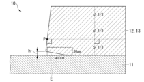
- FIG. 1 is a schematic explanatory diagram of a power module using an insulated circuit board according to an embodiment of the present invention
- FIG. FIG. 4 is an enlarged explanatory view of end portions of the circuit layer and the metal layer of the insulated circuit board according to the embodiment of the present invention
- FIG. 2 is an enlarged explanatory view of a bonding interface between a circuit layer and a metal layer of an insulated circuit board and a ceramic substrate according to an embodiment of the present invention
- FIG. 3B is an enlarged view of an end portion of a bonding interface in the insulating circuit board of FIG. 3A
- 3B is an enlarged view of the central portion of the bonding interface in the insulating circuit board of FIG. 3A
- FIG. 1 is a flowchart of a method for manufacturing an insulated circuit board according to an embodiment of the present invention
- FIG. It is a schematic explanatory drawing of the manufacturing method of the insulation circuit board which concerns on embodiment of this invention.
- the copper/ceramic bonded body according to the present embodiment includes a ceramic substrate 11 as a ceramic member made of ceramics, and a copper plate 42 (circuit layer 12) and a copper plate 43 (metal layer 13) as copper members made of copper or a copper alloy. is an insulating circuit board 10 formed by bonding the .
- FIG. 1 shows a power module 1 having an insulated circuit board 10 according to this embodiment.
- This power module 1 includes an insulating circuit board 10 on which a circuit layer 12 and a metal layer 13 are arranged, and a semiconductor element 3 bonded to one surface (upper surface in FIG. 1) of the circuit layer 12 via a bonding layer 2. and a heat sink 5 arranged on the other side (lower side in FIG. 1) of the metal layer 13 .
- the semiconductor element 3 is made of a semiconductor material such as Si.
- the semiconductor element 3 and the circuit layer 12 are bonded via the bonding layer 2 .
- the bonding layer 2 is made of, for example, a Sn--Ag-based, Sn--In-based, or Sn--Ag--Cu-based solder material.
- the heat sink 5 is for dissipating heat from the insulating circuit board 10 described above.
- the heat sink 5 is made of copper or a copper alloy, and is made of phosphorus-deoxidized copper in this embodiment.
- the heat sink 5 is provided with a channel through which cooling fluid flows.
- the heat sink 5 and the metal layer 13 are joined by a solder layer 7 made of a solder material.
- the solder layer 7 is made of, for example, a Sn--Ag-based, Sn--In-based, or Sn--Ag--Cu-based solder material.
- the insulating circuit board 10 of the present embodiment includes a ceramic substrate 11, a circuit layer 12 provided on one surface (upper surface in FIG. 1) of the ceramic substrate 11, and a ceramic substrate. and a metal layer 13 disposed on the other surface (lower surface in FIG. 1) of the substrate 11 .
- the ceramics substrate 11 is made of ceramics such as silicon nitride (Si 3 N 4 ), aluminum nitride (AlN), alumina (Al 2 O 3 ), etc., which are excellent in insulation and heat dissipation.
- the ceramic substrate 11 is made of aluminum nitride (AlN), which has excellent heat dissipation properties.
- the thickness of the ceramic substrate 11 is set within a range of, for example, 0.2 mm or more and 1.5 mm or less, and is set to 0.635 mm in this embodiment.
- the circuit layer 12 is formed by bonding a copper plate 42 made of copper or a copper alloy to one surface (upper surface in FIG. 5) of the ceramic substrate 11. As shown in FIG. In this embodiment, the circuit layer 12 is formed by bonding a rolled plate of oxygen-free copper to the ceramic substrate 11 .
- the thickness of the copper plate 42 that forms the circuit layer 12 is set within a range of 0.1 mm or more and 2.0 mm or less, and is set to 0.6 mm in this embodiment.
- the metal layer 13 is formed by bonding a copper plate 43 made of copper or a copper alloy to the other surface (lower surface in FIG. 5) of the ceramic substrate 11. As shown in FIG. In this embodiment, the metal layer 13 is formed by bonding a rolled plate of oxygen-free copper to the ceramic substrate 11 .
- the thickness of the copper plate 43 that forms the metal layer 13 is set within a range of 0.1 mm or more and 2.0 mm or less, and is set to 0.6 mm in this embodiment.
- a distance h between the substrate 11 and the circuit layer 12 and the metal layer 13 is in the range of 3 ⁇ m or more and 30 ⁇ m or less. Furthermore, in the insulating circuit board 10 of the present embodiment, as shown in FIG. The void ratio is set to 10% or less.
- the end region in the present embodiment means that, as shown in FIG. 2 , the end region in the present embodiment means that, as shown in FIG. From the surface of the ceramic substrate 11 to the circuit layer 12 and the metal layer 13 side, starting from the intersection point P of the ceramic substrate 11 and the perpendicular line from the end face position of the circuit layer 12 and the metal layer 13 at the position of 1/3 of the thickness of the ceramic substrate 13 The area has a height of 30 ⁇ m and a width of 400 ⁇ m toward the central portion of the circuit layer 12 and the metal layer 13 along the surface of the ceramic substrate 11 .
- the end region means the position of the circuit layer 12 and the metal layer 13 at a position 1 ⁇ 3 of the thickness of the circuit layer 12 and the metal layer 13 from the ceramic substrate 11 . 1/3 of the thickness of the circuit layer 12 and the metal layer 13 from the surface of the ceramic substrate 11 to the circuit layer 12 and the metal layer 13 side, starting from the intersection P of the perpendicular line from the end face position of the layer 13 and the ceramic substrate 11 and a width of 400 ⁇ m along the surface of the ceramic substrate 11 toward the central portion of the circuit layer 12 and the metal layer 13 . Furthermore, the void fraction is calculated as follows.
- the region where the metal constituting the circuit layer 12 and the metal layer 13 does not exist is defined as the void portion, and the ratio of the void portion in the above-mentioned end region is defined as the void ratio.
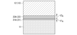
- the active metal compound layers are sequentially formed from the ceramic substrate 11 side.
- 21 and an Ag—Cu alloy layer 22 are preferably formed.
- the active metal compound layer 21 is part of the ceramic substrate (ceramic member) 11 .
- the Ag—Cu alloy layer 22 is part of the circuit layer (copper member) 12 and the metal layer (copper member) 13 . Therefore, the bonding interface between the ceramic substrate 11 and the circuit layer 12 and metal layer 13 (copper plates 42 and 43) is the interface between the active metal compound layer 21 and the Ag--Cu alloy layer 22.
- FIG. Without the Ag—Cu alloy layer 22, the bonding interface between the ceramic substrate 11 and the circuit layer 12 and the metal layer 13 (copper plates 42 and 43) is the active metal compound layer 21, the circuit layer 12 and the metal layer 13 (copper plate 42 , 43).
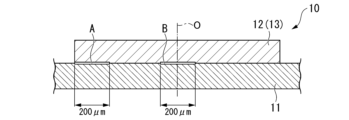
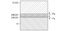
- the end A of the bonding interface between the ceramic substrate 11 and the circuit layer 12 and the metal layer 13 is located in the lamination direction of the circuit layer 12 and the metal layer 13 and the ceramic substrate 11, as shown in FIG. 3A. 200 ⁇ m inward in the width direction from the width direction end portions of the circuit layer 12 and the metal layer 13 in the cross section along .
- the central portion B of the bonding interface between the ceramic substrate 11, the circuit layer 12, and the metal layer 13 is a cross section along the lamination direction of the circuit layer 12, the metal layer 13, and the ceramic substrate 11. , a region of 200 ⁇ m in the width direction including the centers of the circuit layer 12 and the metal layer 13 in the width direction.
- the thickness t1B of the active metal compound layer 21B formed in the central portion B of the bonding interface with the metal layer 13 is set to be in the range of 0.05 ⁇ m or more and 1.2 ⁇ m or less, and the thickness ratio t1A /t1 B is preferably in the range of 0.7 or more and 1.4 or less.
- the active metal compound layers 21A and 21B are layers made of compounds of active metals (one or more selected from Ti, Zr, Nb, and Hf) used in the bonding material 45 . More specifically, when the ceramic substrate is made of silicon nitride (Si 3 N 4 ) or aluminum nitride (AlN), the layer becomes a nitride of these active metals, and the ceramic substrate is made of alumina (Al 2 O 3 ), the layer consists of oxides of these active metals.
- the active metal compound layers 21A and 21B are formed by aggregating active metal compound particles. The average particle size of these particles is 10 nm or more and 100 nm or less.
- the bonding material 45 contains Ti as an active metal and the ceramic substrate 11 is made of aluminum nitride
- the active metal compound layers 21 (21A, 21B) are made of titanium nitride (TiN). Configured. That is, particles of titanium nitride (TiN) having an average particle diameter of 10 nm or more and 100 nm or less are aggregated and formed.
- the thickness t2B of the Ag—Cu alloy layer 22B formed in the central portion B of the bonding interface between the layer 12 and the metal layer 13 is set within a range of 3 ⁇ m or more and 30 ⁇ m or less, and the thickness ratio t2A /t2 B is preferably in the range of 0.7 or more and 1.4 or less.
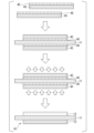
- FIG. 1 A method for manufacturing the insulating circuit board 10 according to the present embodiment will be described below with reference to FIGS. 4 and 5.
- FIG. 1 A method for manufacturing the insulating circuit board 10 according to the present embodiment will be described below with reference to FIGS. 4 and 5.
- a copper plate 42 to be the circuit layer 12 and a copper plate 43 to be the metal layer 13 are prepared.
- a chamfered portion is formed on the peripheral portion of the surface facing the ceramic substrate 11 side.
- a bonding material 45 is applied to the bonding surfaces of the copper plate 42 to be the circuit layer 12 and the copper plate 43 to be the metal layer 13 and dried.
- the coating thickness of the paste-like bonding material 45 is preferably within the range of 10 ⁇ m or more and 50 ⁇ m or less after drying. In this embodiment, the paste bonding material 45 is applied by screen printing.
- the bonding material 45 contains Ag and an active metal (one or more selected from Ti, Zr, Nb, and Hf).
- an Ag--Ti based brazing material (Ag--Cu--Ti based brazing material) is used as the bonding material 45.
- Ag--Ti-based brazing material (Ag--Cu--Ti-based brazing material)
- Cu is in the range of 0 mass% or more and 45 mass% or less
- Ti which is an active metal
- the Ag equivalent film thickness and the mass ratio Ag/active metal between Ag and active metal are adjusted. This makes it possible to control the absolute amount and fluidity of the Ag—Cu liquid phase generated in the pressurization and heating step S03, which will be described later.
- the equivalent film thickness of Ag is preferably 2.5 ⁇ m or more, more preferably 3.5 ⁇ m or more.
- the equivalent film thickness of Ag is preferably 20 ⁇ m or less, more preferably 15 ⁇ m or less.
- the mass ratio Ag/active metal of Ag to active metal is preferably 8 or more, more preferably 12 or more.
- the mass ratio Ag/active metal between Ag and active metal is preferably 60 or less, more preferably 45 or less.
- the specific surface area of the Ag powder contained in the bonding material 45 is preferably 0.15 m 2 /g or more, more preferably 0.25 m 2 /g or more, and more preferably 0.40 m 2 /g or more. is more preferable.
- the specific surface area of the Ag powder contained in the bonding material 45 is preferably 1.40 m 2 /g or less, more preferably 1.00 m 2 /g or less, and 0.75 m 2 /g or less. is more preferable.
- the particle size of the Ag powder contained in the paste-like bonding material 45 preferably has a D10 of 0.7 ⁇ m or more and 3.5 ⁇ m or less and a D100 of 4.5 ⁇ m or more and 23 ⁇ m or less. In the particle size distribution measured by the laser diffraction scattering particle size distribution measurement method, D10 is the particle size at which the cumulative frequency is 10% on a volume basis, and D100 is the particle size at which the cumulative frequency is 100% on a volume basis. be.
- a copper plate 42 to be the circuit layer 12 is laminated on one surface of the ceramic substrate 11 (upper surface in FIG. 5) with a bonding material 45 interposed therebetween, and on the other surface of the ceramic substrate 11 (lower surface in FIG. 5).
- a copper plate 43 to be the metal layer 13 is laminated with a bonding material 45 interposed therebetween.
- the chamfered portions are formed on the peripheral edge portions of the copper plate 42 that forms the circuit layer 12 and the copper plate 43 that forms the metal layer 13 , a gap is formed at the end portion of the ceramic substrate 11 .
- the heating temperature in the pressurizing and heating step S03 is preferably in the range of 800° C. or higher and 850° C. or lower. It is preferable that the sum of the temperature integral values in the heating step from 780° C. to the heating temperature and the holding step at the heating temperature be in the range of 7° C.h or more and 80° C.h or less.
- the pressure load in the pressurization and heating step S03 is preferably within the range of 0.029 MPa or more and 2.94 MPa or less.
- the degree of vacuum in the pressurizing and heating step S03 is preferably in the range of 1 ⁇ 10 ⁇ 6 Pa or more and 5 ⁇ 10 ⁇ 2 Pa or less.
- the cooling rate in this cooling step S04 is preferably within the range of 2° C./min or more and 20° C./min or less.
- the cooling rate here is the cooling rate from the heating temperature to 780° C., which is the Ag—Cu eutectic temperature.
- the insulated circuit board 10 of the present embodiment is manufactured through the bonding material disposing step S01, the laminating step S02, the pressurizing and heating step S03, and the cooling step S04.
- Heat-sink bonding step S05 Next, the heat sink 5 is bonded to the other side of the metal layer 13 of the insulated circuit board 10 .
- the insulating circuit board 10 and the heat sink 5 are laminated with a solder material interposed therebetween and placed in a heating furnace.
- semiconductor element bonding step S06 Next, the semiconductor element 3 is soldered to one surface of the circuit layer 12 of the insulating circuit board 10 .
- the power module 1 shown in FIG. 1 is produced by the above-described steps.
- the circuit layer 12 and the metal layer 13 at the bonding interface between the ceramic substrate 11 and the circuit layer 12 and the metal layer 13, the circuit layer 12 and the metal layer.
- the distance h between the ceramic substrate 11 and the circuit layer 12 and the metal layer 13 at the end of the circuit layer 13 is set to 3 ⁇ m or more, and the void ratio in the end region of the circuit layer 12 and the metal layer 13 is set to 10% or less. Therefore, the thickness of the bonding layer on the end surface is ensured, and the strength of the end portions of the circuit layer 12 and the metal layer 13 can be sufficiently ensured. Therefore, it is possible to suppress cracking and peeling of the ceramic substrate 11 when a thermal cycle is applied.
- the distance h between the ceramic substrate 11 and the circuit layer 12 and the metal layer 13 at the ends of the circuit layer 12 and the metal layer 13 is 30 ⁇ m or less, the protrusion of the bonding material 45 can be suppressed. It is possible to suppress the occurrence of stains.
- the distance h between the ceramic substrate 11 and the circuit layer 12 and metal layer 13 at the ends of the circuit layer 12 and metal layer 13 is preferably 5 ⁇ m or more, more preferably 8 ⁇ m or more.
- the distance h between the ceramic substrate 11 and the circuit layer 12 and metal layer 13 at the ends of the circuit layer 12 and metal layer 13 is preferably 25 ⁇ m or less, more preferably 20 ⁇ m or less.
- the void ratio in the end region E of the circuit layer 12 and the metal layer 13 at the bonding interface between the ceramic substrate 11 and the circuit layer 12 and the metal layer 13 is preferably 8% or less, and preferably 5% or less. is more preferred.
- the thickness t1 A of the active metal compound layer 21A formed at the end portion A of the circuit layer 12 and the metal layer 13 , and the thickness t1 A formed at the central portion B of the circuit layer 12 and the metal layer 13 When the thickness t1B of the active metal compound layer 21B is in the range of 0.05 ⁇ m or more and 1.2 ⁇ m or less, the ceramic substrate 11, the circuit layer 12 and the metal layer 13 are reliably firmly bonded by the active metal. , and hardening of the bonding interface is further suppressed.
- the thickness t1 A of the active metal compound layer 21A formed at the end A of the circuit layer 12 and the metal layer 13 is preferably 0.08 ⁇ m or more, more preferably 0.15 ⁇ m or more.
- the thickness t1B of the active metal compound layer 21B formed in the central portion B of the metal layer 13 is preferably 1.0 ⁇ m or less, more preferably 0.6 ⁇ m or less.
- the thickness t1 A of the active metal compound layer 21A formed at the end A of the circuit layer 12 and the metal layer 13 and the active metal layer 21A formed at the central portion B of the circuit layer 12 and the metal layer 13 When the thickness ratio t1A / t1B to the thickness t1B of the compound layer 21B is in the range of 0.7 to 1.4, the ends A of the circuit layer 12 and the metal layer 13 There is no large difference in the hardness of the joint interface between the center portion b and the occurrence of cracks in the ceramic substrate 11 during thermal cycle loads.
- the thickness t1 A of the active metal compound layer 21A formed at the end A of the circuit layer 12 and the metal layer 13, and Further, the ratio t1A / t1B of the thickness t1B of the active metal compound layer 21B formed in the central portion B of the circuit layer 12 and the metal layer 13 is in the range of 0.8 or more and 1.2 or less. Preferably, it is more preferably in the range of 0.9 or more and 1.1 or less.
- the thickness t2 A of the Ag—Cu alloy layer 22A formed at the end A of the circuit layer 12 and the metal layer 13 and the thickness t2 A formed at the central portion B of the circuit layer 12 and the metal layer 13 When the thickness t2B of the Ag—Cu alloy layer 22B is in the range of 3 ⁇ m or more and 30 ⁇ m or less, the Ag of the bonding material 45, which will be described later, reacts sufficiently with the circuit layer 12 and the metal layer 13. , the ceramic substrate 11, the circuit layer 12 and the metal layer 13 are reliably and strongly bonded together, and hardening of the bonding interface is further suppressed.
- the Ag—Cu alloy layer 22A formed at the end A of the circuit layer 12 and the metal layer 13 should have a thickness t2 A
- the thickness t2B of the Ag—Cu alloy layer 22B formed in the center portion B of the circuit layer 12 and the metal layer 13 is preferably 5 ⁇ m or more, more preferably 7 ⁇ m or more.
- the thickness t2 A of the Ag—Cu alloy layer 22A formed at the end A of the circuit layer 12 and the metal layer 13 and the thickness t2 A of the circuit layer is preferably 25 ⁇ m or less, more preferably 20 ⁇ m or less.
- the thickness t2 A of the Ag—Cu alloy layer 22A formed at the end A of the circuit layer 12 and the metal layer 13 and the thickness t2 A formed at the central portion B of the circuit layer 12 and the metal layer 13 When the ratio t2 A /t2 B to the thickness t2 B of the Ag—Cu alloy layer 22B is within the range of 0.7 or more and 1.4 or less, the end portions of the circuit layer 12 and the metal layer 13 There is no large difference in the hardness of the bonding interface between A and the central portion B, and cracking of the ceramic substrate under thermal cycle load can be further suppressed.
- the thickness t2A of the Ag—Cu alloy layer 22A formed at the end A of the circuit layer 12 and the metal layer 13 is set within the range of 0.8 or more and 1.2 or less. is more preferable, and more preferably within the range of 0.9 or more and 1.1 or less.
- a power module is configured by mounting a semiconductor element on an insulated circuit board, but the present invention is not limited to this.
- an LED module may be configured by mounting an LED element on the circuit layer of the insulating circuit board, or a thermoelectric module may be configured by mounting a thermoelectric element on the circuit layer of the insulating circuit board.
- the ceramic substrate is made of aluminum nitride ( AlN).
- other ceramic substrates such as silicon nitride (Si 3 N 4 ) may be used.
- Ti was used as an example of the active metal contained in the bonding material. It suffices if it contains the above active metals. These active metals may be contained as hydrides.
- the circuit layer was described as being formed by bonding a rolled plate of oxygen-free copper to a ceramic substrate, but the present invention is not limited to this, and a copper piece punched out of a copper plate is used.
- a circuit layer may be formed by bonding to a ceramic substrate while being arranged in a circuit pattern. In this case, each copper piece should have the interface structure with the ceramic substrate as described above.
- a ceramic substrate (40 mm ⁇ 40 mm) shown in Table 1 was prepared.
- the thickness of AlN and Al 2 O 3 was 0.635 mm, and the thickness of Si 3 N 4 was 0.32 mm.
- a copper plate made of oxygen-free copper and having a thickness of 37 mm ⁇ 37 mm and having a thickness shown in Table 1 was prepared as a copper plate serving as a circuit layer and a metal layer.
- a chamfered portion was formed on the peripheral edge portion on the ceramic substrate side.
- a bonding material was applied to the copper plate that was to become the circuit layer and the metal layer.
- a paste material was used as the bonding material, and the amounts of Ag, Cu, and active metal were as shown in Table 1.
- Table 1 the Ag-equivalent thickness and the mass ratio Ag/active metal between Ag and active metal were adjusted.
- a copper plate which will be the circuit layer, is laminated on one side of the ceramic substrate.
- a copper plate serving as a metal layer was laminated on the other surface of the ceramic substrate.
- This laminate was heated while being pressed in the lamination direction to generate an Ag—Cu liquid phase.
- the pressure load was set to 0.294 MPa, and the temperature integral value was set as shown in Table 1. Then, by cooling the heated laminate, the copper plate serving as the circuit layer, the ceramic substrate, and the metal plate serving as the metal layer were bonded to obtain an insulated circuit substrate (copper/ceramic bonded body).
- the void ratio at the edge the distance between the ceramic substrate and the copper plate at the edge, the active metal compound layer, the Ag—Cu alloy layer, the thermal cycle reliability, The presence or absence of waxy stains was evaluated as follows.
- the insulating circuit substrate described above was subjected to the following cooling and heating cycles, and the presence or absence of cracks in the ceramics was determined by SAT inspection (ultrasonic inspection).
- Table 2 shows the evaluation results.
- the number of occurrences of ceramic cracks in Table 2 means the number of thermal cycles required until ceramic cracks occur.
- AlN and Al 2 O 3 One cycle is a load of ⁇ 40° C. ⁇ 10 min and 150° C. ⁇ 10 min, and SAT inspection is performed every 50 cycles up to 500 cycles.
- Si 3 N 4 One cycle is a load of ⁇ 40° C. ⁇ 10 min and 150° C. ⁇ 10 min, and SAT inspection is performed every 200 cycles up to 2000 cycles.
- Comparative Example 1 and Examples 1-3 of the present invention using AlN as the ceramic substrate are compared.
- the distance between the ceramic substrate and the circuit layer (metal layer) at the edge of the circuit layer (metal layer) was 23.2 ⁇ m, and the void ratio in the edge region of the circuit layer (metal layer) was is 16.3%, and the number of cracks generated was 100 times in the thermal cycle test. Wax stains were also confirmed.
- Example 1 of the present invention the distance between the ceramic substrate and the circuit layer (metal layer) at the end of the circuit layer (metal layer) was set to 24.7 ⁇ m.
- the void ratio in the end region is set to 9.8%, and the number of cracks generated was 400 times in the thermal cycle test. Moreover, no wax stain was observed.
- Example 2 of the present invention the distance between the ceramic substrate and the circuit layer (metal layer) at the edge of the circuit layer (metal layer) was 20.9 ⁇ m, and the voids in the edge region of the circuit layer (metal layer) The ratio is 5.3%, and the number of cracks generated was 450 times in the thermal cycle test. Moreover, no wax stain was observed.
- the distance between the ceramic substrate and the circuit layer (metal layer) at the edge of the circuit layer (metal layer) was 12.1 ⁇ m, and the voids in the edge region of the circuit layer (metal layer) The ratio is 0.8%, and the number of cracks generated was 500 times in the thermal cycle test. Moreover, no wax stain was observed.
- Comparative Example 2 Inventive Examples 4-6 using Si 3 N 4 as the ceramic substrate and Comparative Example 2 are compared.
- Comparative Example 2 the distance between the ceramic substrate and the circuit layer (metal layer) at the edge of the circuit layer (metal layer) was 45.1 ⁇ m, and the void ratio in the edge region of the circuit layer (metal layer) was is 13.2%, and the number of cracks generated was 1200 times in the thermal cycle test. Wax stains were also confirmed.
- Example 4 of the present invention the distance between the ceramic substrate and the circuit layer (metal layer) at the end of the circuit layer (metal layer) was set to 3.2 ⁇ m.
- the void ratio in the end region is set to 0.3%, and the number of cracks generated was 1600 times in the thermal cycle test. Moreover, no wax stain was observed.
- the distance between the ceramic substrate and the circuit layer (metal layer) at the edge of the circuit layer (metal layer) was set to 6.4 ⁇ m, and the voids in the edge region of the circuit layer (metal layer) The rate is 7.1%, and the number of cracks generated was 1800 in the thermal cycle test. Moreover, no wax stain was observed.
- Example 6 of the present invention the distance between the ceramic substrate and the circuit layer (metal layer) at the edge of the circuit layer (metal layer) was set to 8.1 ⁇ m, and the voids in the edge region of the circuit layer (metal layer) The ratio is set to 0.1%, and cracks did not occur even after 2000 cycles in the thermal cycle test. Moreover, no wax stain was observed.
- Comparative Example 3 the distance between the ceramic substrate and the circuit layer (metal layer) at the edge of the circuit layer (metal layer) was set to 1.3 ⁇ m, and the void ratio in the edge region of the circuit layer (metal layer) was is 0.0%, and the number of cracks generated was 50 times in the thermal cycle test. No wax stain was observed.
- Example 7 of the present invention the distance between the ceramic substrate and the circuit layer (metal layer) at the end of the circuit layer (metal layer) was set to 29.6 ⁇ m.
- the void ratio in the end region is set to 8.2%, and the number of cracks generated was 350 times in the thermal cycle test. Moreover, no wax stain was observed.
- Example 8 of the present invention the distance between the ceramic substrate and the circuit layer (metal layer) at the edge of the circuit layer (metal layer) was 19.6 ⁇ m, and the voids in the edge region of the circuit layer (metal layer) rate is 4.8%, and the number of cracks generated was 450 times in the thermal cycle test. Moreover, no wax stain was observed.
- ADVANTAGE OF THE INVENTION it is possible to provide a copper/ceramic bonded body excellent in thermal cycle reliability and sufficiently inhibiting the occurrence of brazing stains, and an insulated circuit board made of this copper/ceramic bonded body. .
- Insulated circuit board (copper/ceramic joint) 11 Ceramic substrate (ceramic member) 12 circuit layer (copper member) 13 metal layer (copper member) 21 (21A, 21B) active metal compound layer 22 (22A, 22B) Ag—Cu alloy layer
Landscapes
- Engineering & Computer Science (AREA)
- Chemical & Material Sciences (AREA)
- Microelectronics & Electronic Packaging (AREA)
- Ceramic Engineering (AREA)
- Computer Hardware Design (AREA)
- Power Engineering (AREA)
- Physics & Mathematics (AREA)
- Condensed Matter Physics & Semiconductors (AREA)
- General Physics & Mathematics (AREA)
- Structural Engineering (AREA)
- Organic Chemistry (AREA)
- Materials Engineering (AREA)
- Inorganic Chemistry (AREA)
- Ceramic Products (AREA)
- Cooling Or The Like Of Semiconductors Or Solid State Devices (AREA)
- Parts Printed On Printed Circuit Boards (AREA)
Abstract
Description
本願は、2021年7月30日に、日本に出願された特願2021-125531号に基づき優先権を主張し、その内容をここに援用する。
例えば、風力発電、電気自動車、ハイブリッド自動車等を制御するために用いられる大電力制御用のパワー半導体素子は、動作時の発熱量が多いことから、これを搭載する基板としては、セラミックス基板と、このセラミックス基板の一方の面に導電性の優れた金属板を接合して形成した回路層と、セラミックス基板の他方の面に金属板を接合して形成した放熱用の金属層と、を備えた絶縁回路基板が、従来から広く用いられている。
また、特許文献2においては、銅又は銅合金からなる銅板と、AlN又はAl2O3からなるセラミックス基板とが、AgおよびTiを含む接合材を用いて接合されたパワーモジュール用基板が提案されている。
ここで、銅板とセラミックス基板とを接合した絶縁回路基板において、特許文献3に記載されたように、回路層に張出部を形成した場合には、冷熱サイクルを負荷した際に、熱応力が回路層の端部に集中し、接合信頼性が低下するおそれがあった。
また、前記銅部材の端部における前記セラミックス部材と前記銅部材との間の距離が30μm以下とされているので、接合材のはみ出しを抑制でき、「ろう染み」の発生を抑制することができる。
そして、厚さ比t1A/t1Bが0.7以上1.4以下の範囲内とされているので、前記銅部材の端部と中央部とで接合界面の硬さに大きな差が生じず、冷熱サイクル負荷時におけるセラミックス部材の割れの発生をさらに抑制することができる。
そして、厚さ比t2A/t2Bが、0.7以上1.4以下の範囲内とされているので、前記銅部材の端部と中央部とで接合界面の硬さに大きな差が生じず、冷熱サイクル負荷時におけるセラミックス部材の割れの発生をさらに抑制することができる。
また、前記銅板の端部における前記セラミックス基板と前記銅板との間の距離が30μm以下とされているので、接合材のはみ出しを抑制でき、「ろう染み」の発生を抑制することができる。
そして、厚さ比t1A/t1Bが0.7以上1.4以下の範囲内とされているので、前記銅板の端部と中央部とで接合界面の硬さに大きな差が生じず、冷熱サイクル負荷時におけるセラミックス基板の割れの発生をさらに抑制することが可能となる。
そして、厚さ比t2A/t2Bが、0.7以上1.4以下の範囲内とされているので前記銅板の端部と中央部とで接合界面の硬さに大きな差が生じず、冷熱サイクル負荷時におけるセラミックス基板の割れの発生をさらに抑制することができる。
本実施形態に係る銅/セラミックス接合体は、セラミックスからなるセラミックス部材としてのセラミックス基板11と、銅又は銅合金からなる銅部材としての銅板42(回路層12)および銅板43(金属層13)とが接合されてなる絶縁回路基板10である。図1に、本実施形態である絶縁回路基板10を備えたパワーモジュール1を示す。
接合層2は、例えばSn-Ag系、Sn-In系、若しくはSn-Ag-Cu系のはんだ材で構成されている。
なお、本実施形態においては、ヒートシンク5と金属層13とが、はんだ材からなるはんだ層7によって接合されている。このはんだ層7は、例えばSn-Ag系、Sn-In系、若しくはSn-Ag-Cu系のはんだ材で構成されている。
本実施形態においては、回路層12は、無酸素銅の圧延板がセラミックス基板11に接合されることで形成されている。
なお、回路層12となる銅板42の厚さは0.1mm以上2.0mm以下の範囲内に設定されており、本実施形態では、0.6mmに設定されている。
本実施形態においては、金属層13は、無酸素銅の圧延板がセラミックス基板11に接合されることで形成されている。
なお、金属層13となる銅板43の厚さは0.1mm以上2.0mm以下の範囲内に設定されており、本実施形態では、0.6mmに設定されている。
さらに、本実施形態である絶縁回路基板10においては、図2に示すように、セラミックス基板11と回路層12および金属層13との接合界面の回路層12および金属層13の端部領域Eにおけるボイド率が10%以下とされている。
さらに、ボイド率は、以下のように算出される。上述の端部領域において、回路層12および金属層13を構成する金属が存在しない領域をボイド部とし、上述の端部領域におけるボイド部が占める割合をボイド率とした。
活性金属化合物層21は、セラミックス基板(セラミックス部材)11の一部であると言うこともできる。Ag-Cu合金層22は、回路層(銅部材)12および金属層(銅部材)13の一部であると言うこともできる。このため、セラミックス基板11と回路層12および金属層13(銅板42,43)との接合界面は、活性金属化合物層21とAg-Cu合金層22との界面である。Ag-Cu合金層22を有しない場合、セラミックス基板11と回路層12および金属層13(銅板42,43)との接合界面は、活性金属化合物層21と回路層12および金属層13(銅板42,43)との界面である。
なお、本実施形態において、セラミックス基板11と回路層12および金属層13との接合界面の端部Aは、図3Aに示すように、回路層12および金属層13とセラミックス基板11との積層方向に沿った断面において、回路層12および金属層13の幅方向端部から幅方向内方に200μmまでの領域である。
また、セラミックス基板11と回路層12および金属層13との接合界面の中央部Bは、図3Aに示すように、回路層12および金属層13とセラミックス基板11との積層方向に沿った断面において、回路層12および金属層13の幅方向中心を含む幅方向200μmの領域である。
なお、本実施形態では、接合材45が活性金属としてTiを含有し、セラミックス基板11が窒化アルミニウムで構成されているため、活性金属化合物層21(21A,21B)は、窒化チタン(TiN)で構成される。すなわち、平均粒径が10nm以上100nm以下の窒化チタン(TiN)の粒子が集合して形成されている。
回路層12となる銅板42と、金属層13となる銅板43とを準備する。ここで、回路層12となる銅板42および金属層13となる銅板43においては、セラミックス基板11側の向く面の周縁部に面取り部が形成されている。
そして、回路層12となる銅板42および金属層13となる銅板43の接合面に、接合材45を塗布し、乾燥させる。ペースト状の接合材45の塗布厚さは、乾燥後で10μm以上50μm以下の範囲内とすることが好ましい。
本実施形態では、スクリーン印刷によってペースト状の接合材45を塗布する。
具体的には、Agの換算膜厚を2.5μm以上とすることが好ましく、3.5μm以上とすることがさらに好ましい。一方、Agの換算膜厚を20μm以下とすることが好ましく、15μm以下とすることがさらに好ましい。
また、Agと活性金属の質量比Ag/活性金属を8以上とすることが好ましく、12以上とすることがさらに好ましい。一方、Agと活性金属の質量比Ag/活性金属を60以下とすることが好ましく、45以下とすることがさらに好ましい。
なお、ペースト状の接合材45に含まれるAg粉の粒径は、D10が0.7μm以上3.5μm以下、かつ、D100が4.5μm以上23μm以下の範囲内であることが好ましい。レーザー回折散乱式粒度分布測定法によって測定された粒度分布において、D10は、体積基準で累積頻度が10%になる粒径であり、D100は、体積基準で累積頻度が100%になる粒径である。
次に、セラミックス基板11の一方の面(図5において上面)に、接合材45を介して回路層12となる銅板42を積層するとともに、セラミックス基板11の他方の面(図5において下面)に、接合材45を介して金属層13となる銅板43を積層する。なお、回路層12となる銅板42および金属層13となる銅板43の周縁部に面取り部が形成されているので、セラミックス基板11の端部に空隙が形成されることになる。
次に、銅板42とセラミックス基板11と銅板43とを加圧した状態で、真空雰囲気の加熱炉内で加熱し、接合材45を溶融する。
ここで、加圧および加熱工程S03における加熱温度は、800℃以上850℃以下の範囲内とすることが好ましい。780℃から加熱温度までの昇温工程および加熱温度での保持工程における温度積分値の合計が7℃・h以上80℃・h以下の範囲内とすることが好ましい。
また、加圧および加熱工程S03における加圧荷重は、0.029MPa以上2.94MPa以下の範囲内とすることが好ましい。
さらに、加圧および加熱工程S03における真空度は、1×10⁻⁶Pa以上5×10⁻²Pa以下の範囲内とすることが好ましい。
そして、加圧および加熱工程S03の後、冷却を行うことにより、溶融した接合材45を凝固させて、回路層12となる銅板42とセラミックス基板11、セラミックス基板11と金属層13となる銅板43とを接合する。
なお、この冷却工程S04における冷却速度は、2℃/min以上20℃/min以下の範囲内とすることが好ましい。なお、ここでの冷却速度は加熱温度からAg-Cu共晶温度である780℃までの冷却速度である。
次に、絶縁回路基板10の金属層13の他方の面側にヒートシンク5を接合する。
絶縁回路基板10とヒートシンク5とを、はんだ材を介して積層して加熱炉に装入し、はんだ層7を介して絶縁回路基板10とヒートシンク5とをはんだ接合する。
次に、絶縁回路基板10の回路層12の一方の面に、半導体素子3をはんだ付けにより接合する。
前述の工程により、図1に示すパワーモジュール1が製出される。
また、回路層12および金属層13の端部におけるセラミックス基板11と回路層12および金属層13との間の距離hが30μm以下とされているので、接合材45のはみ出しを抑制でき、「ろう染み」の発生を抑制することができる。
また、セラミックス基板11と回路層12および金属層13との接合界面の回路層12および金属層13の端部領域Eにおけるボイド率は、8%以下であることが好ましく、5%以下であることがさらに好ましい。
また、接合界面が硬くなることがさらに確実に抑制するためには、回路層12および金属層13の端部Aに形成された活性金属化合物層21Aの厚さt1A、および、回路層12および金属層13の中央部Bに形成された活性金属化合物層21Bの厚さt1Bを、1.0μm以下とすることが好ましく、0.6μm以下とすることがより好ましい。
また、接合界面が必要以上に硬くなることをさらに抑制するためには、回路層12および金属層13の端部Aに形成されたAg-Cu合金層22Aの厚さt2A、および、回路層12および金属層13の中央部Bに形成されたAg-Cu合金層22Bの厚さt2Bを、25μm以下とすることが好ましく、20μm以下とすることがより好ましい。
例えば、本実施形態では、絶縁回路基板に半導体素子を搭載してパワーモジュールを構成するものとして説明したが、これに限定されることはない。例えば、絶縁回路基板の回路層にLED素子を搭載してLEDモジュールを構成してもよいし、絶縁回路基板の回路層に熱電素子を搭載して熱電モジュールを構成してもよい。
また、回路層および金属層となる銅板として、無酸素銅からなり、表1に示す厚さの37mm×37mmの銅板を準備した。なお、回路層および金属層となる銅板においては、セラミックス基板側の周縁部に面取り部を形成した。
そして、加熱した積層体を冷却することにより、回路層となる銅板とセラミックス基板と金属層となる金属板を接合し、絶縁回路基板(銅/セラミックス接合体)を得た。
回路層とセラミックス基板との接合界面、および、セラミックス基板と金属層との接合界面の端部断面について、EPMA装置(電子プローブマイクロアナライザ)を用いて、Ag、Cu、活性金属の各元素マッピングを取得した。それぞれ5視野で各元素マッピングを取得した。そして、端部領域においてAg、Cu、活性金属が検出されなかった領域の面積(ボイド面積)を求めて、ボイド率=100×ボイド面積/端部領域面積の最大値を「端部のボイド率」とし、表2に記載した。
回路層とセラミックス基板との接合界面、および、セラミックス基板と金属層との接合界面において、上述した端部断面を、EPMA装置を用いて、Ag、Cu、活性金属の各元素のライン分析を実施した。交点Pを通り、かつセラミックス基板に対して垂直な方向に回路層、または金属層に向かって、それぞれ5視野で各元素のライン分析を実施した。そして、Ag+Cu+活性金属=100mass%としたとき、セラミックス基板表面からCu濃度が90mass%以上である領域までの距離を測定し、それぞれ5視野、計10視野の内最も短い距離を「端部におけるセラミックス基板と銅板との間の距離」とし、表2に記載した。
回路層とセラミックス基板との接合界面、および、セラミックス基板と金属層との接合界面の断面を、走査型電子顕微鏡(カールツァイスNTS社製ULTRA55、加速電圧1.8kV)を用いて倍率30000倍で測定し、エネルギー分散型X線分析法により、N、O及び活性金属元素の元素マッピングを取得した。活性金属元素とNまたはOが同一領域に存在する場合に活性金属化合物層が有ると判断した。
それぞれ5視野で観察を行い、活性金属元素とNまたはOが同一領域に存在する範囲の面積を測定した幅で割ったものの平均値を「活性金属化合物層の厚さ」とし表2に記載した。
回路層とセラミックス基板との接合界面、および、セラミックス基板と金属層との接合界面の断面を、EPMA装置を用いて、Ag,Cu,活性金属の各元素マッピングを取得した。それぞれ5視野で各元素マッピングを取得した。
そして、Ag+Cu+活性金属=100mass%としたとき、Ag濃度が15質量%以上である領域をAg-Cu合金層とし、その面積を求めて、測定領域の幅で割った値(面積/測定領域の幅)を求めた。その値の平均をAg-Cu合金層の厚さとして表2に記載した。
上述の絶縁回路基板を、セラミックス基板の材質に応じて、下記の冷熱サイクルを負荷し、SAT検査(超音波探傷検査)によりセラミックス割れの有無を判定した。評価結果を表2に示す。表2のセラミックス割れの発生回数は、セラミックス割れが発生するまでに要した冷熱サイクル数を意味している。
AlN,Al2O3の場合:-40℃×10min、150℃×10minの負荷を1サイクルとし、500サイクルまで50サイクル毎にSAT検査する。
Si3N4の場合:-40℃×10min、150℃×10minの負荷を1サイクルとし、2000サイクルまで200サイクル毎にSAT検査する。
回路層表面および金属層表面を、EPMA装置を用いてAg、Cu、活性金属の各元素マッピングを取得した。そして、Ag+Cu+活性金属=100mass%としたとき、Ag濃度が15質量%以上である領域を「ろう染み」とし、その面積を求めて、回路層及び金属層の外周から100μmの領域の面積で割った値が20%以上の場合に「ろう染み」が有ると判断した。

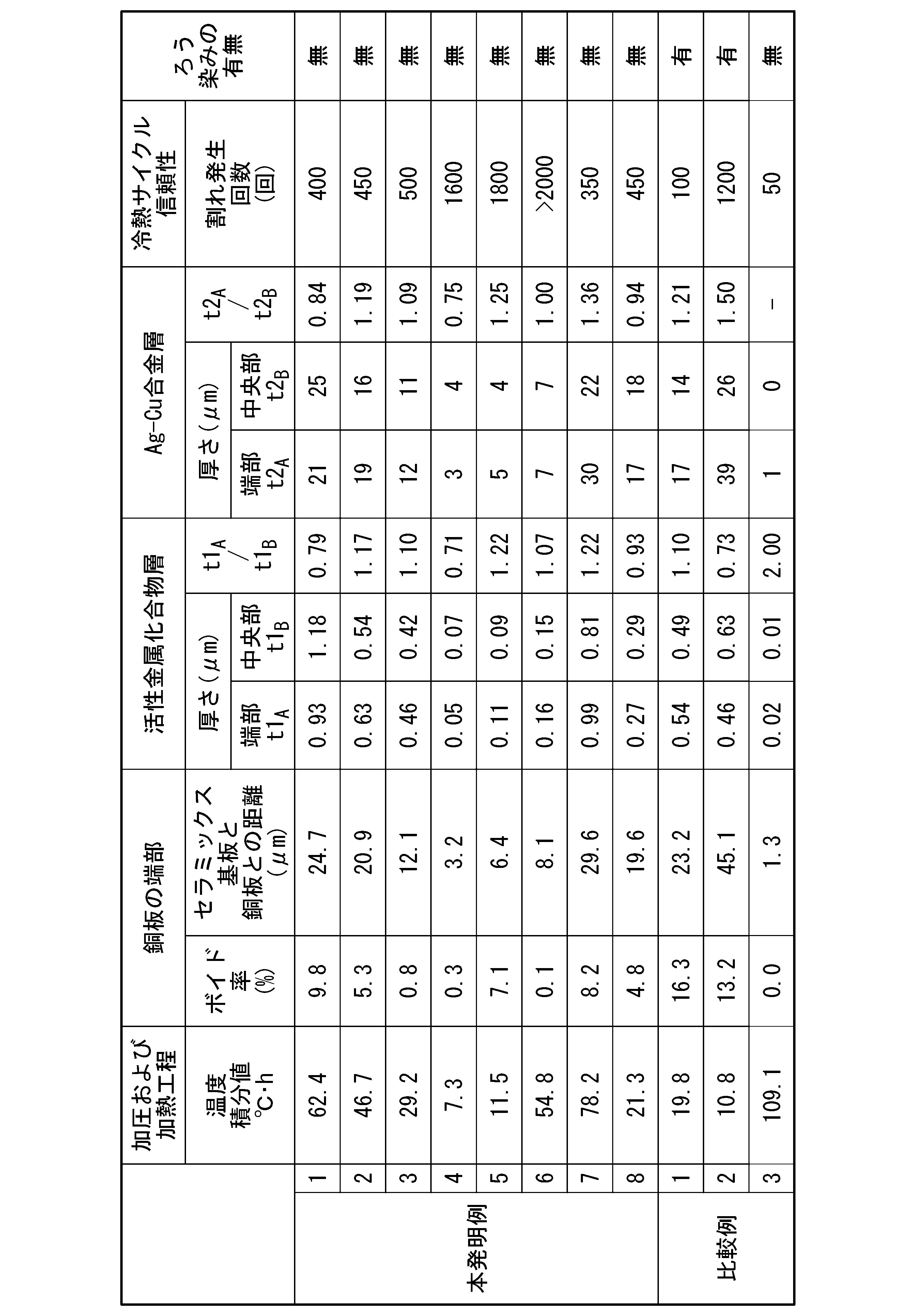
比較例1においては、回路層(金属層)の端部におけるセラミックス基板と回路層(金属層)との間の距離が23.2μmとされ、回路層(金属層)の端部領域におけるボイド率が16.3%とされており、冷熱サイクル試験において割れ発生回数が100回となった。また、ろう染みが確認された。
本発明例2においては、回路層(金属層)の端部におけるセラミックス基板と回路層(金属層)との間の距離が20.9μmとされ、回路層(金属層)の端部領域におけるボイド率が5.3%とされており、冷熱サイクル試験において割れ発生回数が450回となった。また、ろう染みは確認されなかった。
本発明例3においては、回路層(金属層)の端部におけるセラミックス基板と回路層(金属層)との間の距離が12.1μmとされ、回路層(金属層)の端部領域におけるボイド率が0.8%とされており、冷熱サイクル試験において割れ発生回数が500回となった。また、ろう染みは確認されなかった。
比較例2においては、回路層(金属層)の端部におけるセラミックス基板と回路層(金属層)との間の距離が45.1μmとされ、回路層(金属層)の端部領域におけるボイド率が13.2%とされており、冷熱サイクル試験において割れ発生回数が1200回となった。また、ろう染みが確認された。
本発明例5においては、回路層(金属層)の端部におけるセラミックス基板と回路層(金属層)との間の距離が6.4μmとされ、回路層(金属層)の端部領域におけるボイド率が7.1%とされており、冷熱サイクル試験において割れ発生回数が1800回となった。また、ろう染みは確認されなかった。
本発明例6においては、回路層(金属層)の端部におけるセラミックス基板と回路層(金属層)との間の距離が8.1μmとされ、回路層(金属層)の端部領域におけるボイド率が0.1%とされており、冷熱サイクル試験において2000回でも割れが発生しなかった。また、ろう染みは確認されなかった。
比較例3においては、回路層(金属層)の端部におけるセラミックス基板と回路層(金属層)との間の距離が1.3μmとされ、回路層(金属層)の端部領域におけるボイド率が0.0%とされており、冷熱サイクル試験において割れ発生回数が50回となった。なお、ろう染みは確認されなかった。
本発明例8においては、回路層(金属層)の端部におけるセラミックス基板と回路層(金属層)との間の距離が19.6μmとされ、回路層(金属層)の端部領域におけるボイド率が4.8%とされており、冷熱サイクル試験において割れ発生回数が450回となった。また、ろう染みは確認されなかった。
11 セラミックス基板(セラミックス部材)
12 回路層(銅部材)
13 金属層(銅部材)
21(21A,21B) 活性金属化合物層
22(22A,22B) Ag-Cu合金層
Claims (6)
- 銅又は銅合金からなる銅部材と、セラミックス部材とが接合されてなる銅/セラミックス接合体であって、
前記セラミックス部材と前記銅部材との接合界面において、前記銅部材の端部における前記セラミックス部材と前記銅部材との間の距離が3μm以上30μm以下の範囲内とされるとともに、
前記銅部材の端部領域におけるボイド率が10%以下であることを特徴とする銅/セラミックス接合体。 - 前記セラミックス部材と前記銅部材との接合界面において、前記セラミックス部材側には活性金属化合物層が形成されており、
前記銅部材の前記端部における前記活性金属化合物層の厚さt1Aおよび前記銅部材の中央部における前記活性金属化合物層の厚さt1Bが0.05μm以上1.2μm以下の範囲内とされ、厚さ比t1A/t1Bが0.7以上1.4以下の範囲内とされていることを特徴とする請求項1に記載の銅/セラミックス接合体。 - 前記セラミックス部材と前記銅部材との接合界面において、前記銅部材側にはAg-Cu合金層が形成されており、
前記銅部材の前記端部における前記Ag-Cu合金層の厚さt2Aおよび前記銅部材の中央部における前記Ag-Cu合金層の厚さt2Bが3μm以上30μm以下の範囲内とされ、厚さ比t2A/t2Bが0.7以上1.4以下の範囲内とされていることを特徴とする請求項1または請求項2に記載の銅/セラミックス接合体。 - セラミックス基板の表面に、銅又は銅合金からなる銅板が接合されてなる絶縁回路基板であって、
前記セラミックス基板と前記銅板との接合界面において、前記銅板の端部における前記セラミックス基板と前記銅板との間の距離が3μm以上30μm以下の範囲内とされるとともに、
前記銅板の端部領域におけるボイド率が10%以下であることを特徴とする絶縁回路基板。 - 前記セラミックス基板と前記銅板との接合界面において、前記セラミックス基板側には活性金属化合物層が形成されており、
前記銅板の前記端部における前記活性金属化合物層の厚さt1Aおよび前記銅板の中央部における前記活性金属化合物層の厚さt1Bが0.05μm以上1.2μm以下の範囲内とされ、厚さ比t1A/t1Bが0.7以上1.4以下の範囲内とされていることを特徴とする請求項4に記載の絶縁回路基板。 - 前記セラミックス基板と前記銅板との接合界面において、前記銅板側にはAg-Cu合金層が形成されており、
前記銅板の前記端部における前記Ag-Cu合金層の厚さt2Aおよび前記銅板の中央部における前記Ag-Cu合金層の厚さt2Bが3μm以上30μm以下の範囲内とされ、厚さ比t2A/t2Bが0.7以上1.4以下の範囲内とされていることを特徴とする請求項4または請求項5に記載の絶縁回路基板。
Priority Applications (2)
| Application Number | Priority Date | Filing Date | Title |
|---|---|---|---|
| EP22849622.0A EP4378913A1 (en) | 2021-07-30 | 2022-07-29 | Copper/ceramic bonded body and insulated circuit board |
| CN202280051700.6A CN117769533A (zh) | 2021-07-30 | 2022-07-29 | 铜-陶瓷接合体及绝缘电路基板 |
Applications Claiming Priority (2)
| Application Number | Priority Date | Filing Date | Title |
|---|---|---|---|
| JP2021-125531 | 2021-07-30 | ||
| JP2021125531A JP2023020265A (ja) | 2021-07-30 | 2021-07-30 | 銅/セラミックス接合体、および、絶縁回路基板 |
Publications (1)
| Publication Number | Publication Date |
|---|---|
| WO2023008562A1 true WO2023008562A1 (ja) | 2023-02-02 |
Family
ID=85086870
Family Applications (1)
| Application Number | Title | Priority Date | Filing Date |
|---|---|---|---|
| PCT/JP2022/029314 WO2023008562A1 (ja) | 2021-07-30 | 2022-07-29 | 銅/セラミックス接合体、および、絶縁回路基板 |
Country Status (4)
| Country | Link |
|---|---|
| EP (1) | EP4378913A1 (ja) |
| JP (1) | JP2023020265A (ja) |
| CN (1) | CN117769533A (ja) |
| WO (1) | WO2023008562A1 (ja) |
Citations (15)
| Publication number | Priority date | Publication date | Assignee | Title |
|---|---|---|---|---|
| JPH104156A (ja) * | 1996-06-14 | 1998-01-06 | Mitsubishi Electric Corp | 半導体装置用絶縁基板及び半導体装置 |
| JP3211856B2 (ja) | 1994-11-02 | 2001-09-25 | 電気化学工業株式会社 | 回路基板 |
| JP2002274964A (ja) * | 2001-03-13 | 2002-09-25 | Denki Kagaku Kogyo Kk | 接合体の製造方法 |
| JP2003055058A (ja) * | 2001-08-23 | 2003-02-26 | Denki Kagaku Kogyo Kk | セラミック体と銅板の接合方法 |
| JP2014090144A (ja) * | 2012-10-31 | 2014-05-15 | Denki Kagaku Kogyo Kk | セラミック回路基板および製造方法 |
| JP2015092552A (ja) * | 2013-09-30 | 2015-05-14 | 三菱マテリアル株式会社 | Cu/セラミックス接合体、Cu/セラミックス接合体の製造方法、及び、パワーモジュール用基板 |
| JP5957862B2 (ja) | 2011-12-05 | 2016-07-27 | 三菱マテリアル株式会社 | パワーモジュール用基板 |
| JP2016169111A (ja) * | 2015-03-11 | 2016-09-23 | デンカ株式会社 | セラミックス回路基板 |
| WO2017213207A1 (ja) * | 2016-06-10 | 2017-12-14 | 田中貴金属工業株式会社 | セラミックス回路基板、及び、セラミックス回路基板の製造方法 |
| JP2018008869A (ja) * | 2016-06-30 | 2018-01-18 | 三菱マテリアル株式会社 | 銅/セラミックス接合体、及び、絶縁回路基板 |
| WO2018199060A1 (ja) * | 2017-04-25 | 2018-11-01 | デンカ株式会社 | セラミックス回路基板及びその製造方法とそれを用いたモジュール |
| WO2018221493A1 (ja) * | 2017-05-30 | 2018-12-06 | デンカ株式会社 | セラミックス回路基板及びそれを用いたモジュール |
| JP2020053580A (ja) * | 2018-09-27 | 2020-04-02 | 京セラ株式会社 | パワーモジュール用基板およびパワーモジュール |
| JP2021098641A (ja) * | 2019-12-19 | 2021-07-01 | 三菱マテリアル株式会社 | 銅/セラミックス接合体、及び、絶縁回路基板 |
| JP2021125531A (ja) | 2020-02-04 | 2021-08-30 | 株式会社村田製作所 | コモンモードチョークコイル |
-
2021
- 2021-07-30 JP JP2021125531A patent/JP2023020265A/ja active Pending
-
2022
- 2022-07-29 EP EP22849622.0A patent/EP4378913A1/en active Pending
- 2022-07-29 CN CN202280051700.6A patent/CN117769533A/zh active Pending
- 2022-07-29 WO PCT/JP2022/029314 patent/WO2023008562A1/ja active Application Filing
Patent Citations (16)
| Publication number | Priority date | Publication date | Assignee | Title |
|---|---|---|---|---|
| JP3211856B2 (ja) | 1994-11-02 | 2001-09-25 | 電気化学工業株式会社 | 回路基板 |
| JPH104156A (ja) * | 1996-06-14 | 1998-01-06 | Mitsubishi Electric Corp | 半導体装置用絶縁基板及び半導体装置 |
| JP2002274964A (ja) * | 2001-03-13 | 2002-09-25 | Denki Kagaku Kogyo Kk | 接合体の製造方法 |
| JP2003055058A (ja) * | 2001-08-23 | 2003-02-26 | Denki Kagaku Kogyo Kk | セラミック体と銅板の接合方法 |
| JP5957862B2 (ja) | 2011-12-05 | 2016-07-27 | 三菱マテリアル株式会社 | パワーモジュール用基板 |
| JP2014090144A (ja) * | 2012-10-31 | 2014-05-15 | Denki Kagaku Kogyo Kk | セラミック回路基板および製造方法 |
| JP2015092552A (ja) * | 2013-09-30 | 2015-05-14 | 三菱マテリアル株式会社 | Cu/セラミックス接合体、Cu/セラミックス接合体の製造方法、及び、パワーモジュール用基板 |
| JP5757359B2 (ja) | 2013-09-30 | 2015-07-29 | 三菱マテリアル株式会社 | Cu/セラミックス接合体、Cu/セラミックス接合体の製造方法、及び、パワーモジュール用基板 |
| JP2016169111A (ja) * | 2015-03-11 | 2016-09-23 | デンカ株式会社 | セラミックス回路基板 |
| WO2017213207A1 (ja) * | 2016-06-10 | 2017-12-14 | 田中貴金属工業株式会社 | セラミックス回路基板、及び、セラミックス回路基板の製造方法 |
| JP2018008869A (ja) * | 2016-06-30 | 2018-01-18 | 三菱マテリアル株式会社 | 銅/セラミックス接合体、及び、絶縁回路基板 |
| WO2018199060A1 (ja) * | 2017-04-25 | 2018-11-01 | デンカ株式会社 | セラミックス回路基板及びその製造方法とそれを用いたモジュール |
| WO2018221493A1 (ja) * | 2017-05-30 | 2018-12-06 | デンカ株式会社 | セラミックス回路基板及びそれを用いたモジュール |
| JP2020053580A (ja) * | 2018-09-27 | 2020-04-02 | 京セラ株式会社 | パワーモジュール用基板およびパワーモジュール |
| JP2021098641A (ja) * | 2019-12-19 | 2021-07-01 | 三菱マテリアル株式会社 | 銅/セラミックス接合体、及び、絶縁回路基板 |
| JP2021125531A (ja) | 2020-02-04 | 2021-08-30 | 株式会社村田製作所 | コモンモードチョークコイル |
Also Published As
| Publication number | Publication date |
|---|---|
| JP2023020265A (ja) | 2023-02-09 |
| EP4378913A1 (en) | 2024-06-05 |
| CN117769533A (zh) | 2024-03-26 |
Similar Documents
| Publication | Publication Date | Title |
|---|---|---|
| US10818585B2 (en) | Copper/ceramic joined body, insulated circuit board, method for producing copper/ceramic joined body, and method for producing insulated circuit board | |
| KR102422607B1 (ko) | 접합체, 히트 싱크가 부착된 파워 모듈용 기판, 히트 싱크, 및 접합체의 제조 방법, 히트 싱크가 부착된 파워 모듈용 기판의 제조 방법, 히트 싱크의 제조 방법 | |
| US12027434B2 (en) | Bonded body of copper and ceramic, insulating circuit substrate, bonded body of copper and ceramic production method, and insulating circuit substrate production method | |
| JP5991103B2 (ja) | ヒートシンク付パワーモジュール用基板、ヒートシンク付パワーモジュール、及びヒートシンク付パワーモジュール用基板の製造方法 | |
| WO2021033421A1 (ja) | 銅/セラミックス接合体、絶縁回路基板、及び、銅/セラミックス接合体の製造方法、絶縁回路基板の製造方法 | |
| WO2021124923A1 (ja) | 銅/セラミックス接合体、及び、絶縁回路基板 | |
| JP6656657B2 (ja) | セラミックス/アルミニウム接合体、パワーモジュール用基板、及び、パワーモジュール | |
| JP6870767B2 (ja) | 銅/セラミックス接合体、及び、絶縁回路基板 | |
| JP2021098641A (ja) | 銅/セラミックス接合体、及び、絶縁回路基板 | |
| JP2023086688A (ja) | 銅/セラミックス接合体、および、絶縁回路基板 | |
| WO2023008562A1 (ja) | 銅/セラミックス接合体、および、絶縁回路基板 | |
| JP6928297B2 (ja) | 銅/セラミックス接合体、及び、絶縁回路基板 | |
| WO2021117327A1 (ja) | 銅/セラミックス接合体、及び、絶縁回路基板 | |
| WO2023008565A1 (ja) | 銅/セラミックス接合体、および、絶縁回路基板 | |
| WO2016167217A1 (ja) | 接合体、ヒートシンク付パワーモジュール用基板、ヒートシンク、及び、接合体の製造方法、ヒートシンク付パワーモジュール用基板の製造方法、ヒートシンクの製造方法 | |
| WO2023286856A1 (ja) | 銅/セラミックス接合体、および、絶縁回路基板 | |
| WO2023286860A1 (ja) | 銅/セラミックス接合体、および、絶縁回路基板 | |
| JP7039933B2 (ja) | 接合体、絶縁回路基板、ヒートシンク付絶縁回路基板、ヒートシンク、及び、接合体の製造方法、絶縁回路基板の製造方法、ヒートシンク付絶縁回路基板の製造方法、ヒートシンクの製造方法 | |
| WO2023286857A1 (ja) | 銅/セラミックス接合体、および、絶縁回路基板 | |
| WO2023286862A1 (ja) | 銅/セラミックス接合体、および、絶縁回路基板 | |
| JP2021031315A (ja) | 銅/セラミックス接合体、絶縁回路基板、及び、銅/セラミックス接合体の製造方法、絶縁回路基板の製造方法 | |
| WO2022224946A1 (ja) | 銅/セラミックス接合体、および、絶縁回路基板 | |
| WO2023106226A1 (ja) | 銅/セラミックス接合体、および、絶縁回路基板 | |
| JP7424043B2 (ja) | 銅/セラミックス接合体、絶縁回路基板、及び、銅/セラミックス接合体の製造方法、絶縁回路基板の製造方法 | |
| WO2023286858A1 (ja) | 銅/セラミックス接合体、絶縁回路基板、および、銅/セラミックス接合体の製造方法、絶縁回路基板の製造方法 |
Legal Events
| Date | Code | Title | Description |
|---|---|---|---|
| 121 | Ep: the epo has been informed by wipo that ep was designated in this application |
Ref document number: 22849622 Country of ref document: EP Kind code of ref document: A1 |
|
| WWE | Wipo information: entry into national phase |
Ref document number: 202280051700.6 Country of ref document: CN |
|
| WWE | Wipo information: entry into national phase |
Ref document number: 2022849622 Country of ref document: EP |
|
| NENP | Non-entry into the national phase |
Ref country code: DE |
|
| ENP | Entry into the national phase |
Ref document number: 2022849622 Country of ref document: EP Effective date: 20240229 |