WO2016167217A1 - 接合体、ヒートシンク付パワーモジュール用基板、ヒートシンク、及び、接合体の製造方法、ヒートシンク付パワーモジュール用基板の製造方法、ヒートシンクの製造方法 - Google Patents
接合体、ヒートシンク付パワーモジュール用基板、ヒートシンク、及び、接合体の製造方法、ヒートシンク付パワーモジュール用基板の製造方法、ヒートシンクの製造方法 Download PDFInfo
- Publication number
- WO2016167217A1 WO2016167217A1 PCT/JP2016/061686 JP2016061686W WO2016167217A1 WO 2016167217 A1 WO2016167217 A1 WO 2016167217A1 JP 2016061686 W JP2016061686 W JP 2016061686W WO 2016167217 A1 WO2016167217 A1 WO 2016167217A1
- Authority
- WO
- WIPO (PCT)
- Prior art keywords
- heat sink
- layer
- mass
- metal
- aluminum alloy
- Prior art date
Links
Images


Classifications
-
- B—PERFORMING OPERATIONS; TRANSPORTING
- B23—MACHINE TOOLS; METAL-WORKING NOT OTHERWISE PROVIDED FOR
- B23K—SOLDERING OR UNSOLDERING; WELDING; CLADDING OR PLATING BY SOLDERING OR WELDING; CUTTING BY APPLYING HEAT LOCALLY, e.g. FLAME CUTTING; WORKING BY LASER BEAM
- B23K20/00—Non-electric welding by applying impact or other pressure, with or without the application of heat, e.g. cladding or plating
-
- H—ELECTRICITY
- H01—ELECTRIC ELEMENTS
- H01L—SEMICONDUCTOR DEVICES NOT COVERED BY CLASS H10
- H01L23/00—Details of semiconductor or other solid state devices
- H01L23/12—Mountings, e.g. non-detachable insulating substrates
-
- H—ELECTRICITY
- H01—ELECTRIC ELEMENTS
- H01L—SEMICONDUCTOR DEVICES NOT COVERED BY CLASS H10
- H01L23/00—Details of semiconductor or other solid state devices
- H01L23/12—Mountings, e.g. non-detachable insulating substrates
- H01L23/13—Mountings, e.g. non-detachable insulating substrates characterised by the shape
-
- H—ELECTRICITY
- H01—ELECTRIC ELEMENTS
- H01L—SEMICONDUCTOR DEVICES NOT COVERED BY CLASS H10
- H01L23/00—Details of semiconductor or other solid state devices
- H01L23/34—Arrangements for cooling, heating, ventilating or temperature compensation ; Temperature sensing arrangements
- H01L23/36—Selection of materials, or shaping, to facilitate cooling or heating, e.g. heatsinks
-
- H—ELECTRICITY
- H01—ELECTRIC ELEMENTS
- H01L—SEMICONDUCTOR DEVICES NOT COVERED BY CLASS H10
- H01L23/00—Details of semiconductor or other solid state devices
- H01L23/34—Arrangements for cooling, heating, ventilating or temperature compensation ; Temperature sensing arrangements
- H01L23/40—Mountings or securing means for detachable cooling or heating arrangements ; fixed by friction, plugs or springs
-
- H—ELECTRICITY
- H05—ELECTRIC TECHNIQUES NOT OTHERWISE PROVIDED FOR
- H05K—PRINTED CIRCUITS; CASINGS OR CONSTRUCTIONAL DETAILS OF ELECTRIC APPARATUS; MANUFACTURE OF ASSEMBLAGES OF ELECTRICAL COMPONENTS
- H05K7/00—Constructional details common to different types of electric apparatus
- H05K7/20—Modifications to facilitate cooling, ventilating, or heating
-
- H—ELECTRICITY
- H01—ELECTRIC ELEMENTS
- H01L—SEMICONDUCTOR DEVICES NOT COVERED BY CLASS H10
- H01L2224/00—Indexing scheme for arrangements for connecting or disconnecting semiconductor or solid-state bodies and methods related thereto as covered by H01L24/00
- H01L2224/01—Means for bonding being attached to, or being formed on, the surface to be connected, e.g. chip-to-package, die-attach, "first-level" interconnects; Manufacturing methods related thereto
- H01L2224/26—Layer connectors, e.g. plate connectors, solder or adhesive layers; Manufacturing methods related thereto
- H01L2224/31—Structure, shape, material or disposition of the layer connectors after the connecting process
- H01L2224/32—Structure, shape, material or disposition of the layer connectors after the connecting process of an individual layer connector
- H01L2224/321—Disposition
- H01L2224/32151—Disposition the layer connector connecting between a semiconductor or solid-state body and an item not being a semiconductor or solid-state body, e.g. chip-to-substrate, chip-to-passive
- H01L2224/32221—Disposition the layer connector connecting between a semiconductor or solid-state body and an item not being a semiconductor or solid-state body, e.g. chip-to-substrate, chip-to-passive the body and the item being stacked
- H01L2224/32225—Disposition the layer connector connecting between a semiconductor or solid-state body and an item not being a semiconductor or solid-state body, e.g. chip-to-substrate, chip-to-passive the body and the item being stacked the item being non-metallic, e.g. insulating substrate with or without metallisation
Definitions
- a heat sink is joined to a power module substrate in which a circuit layer is formed on one surface of an insulating layer, a joined body in which an aluminum alloy member and a metal member made of copper, nickel, or silver are joined.
- the present invention relates to a power module substrate with a heat sink, a heat sink in which a metal member layer is formed on a heat sink body, a method of manufacturing a joined body, a method of manufacturing a power module substrate with a heat sink, and a method of manufacturing a heat sink.
- Semiconductor devices such as LEDs and power modules have a structure in which a semiconductor element is bonded on a circuit layer made of a conductive material.
- Power semiconductor elements for high power control used for controlling wind power generation, electric vehicles, hybrid vehicles, and the like generate a large amount of heat. Therefore, as a substrate on which a power semiconductor element for high power control is mounted, for example, a ceramic substrate made of AlN (aluminum nitride), Al 2 O 3 (alumina), etc., and one surface of this ceramic substrate has excellent conductivity.
- a power module substrate including a circuit layer formed by bonding metal plates has been widely used.
- a substrate having a metal layer formed on the other surface of a ceramic substrate is also provided.
- a power module substrate in which a circuit layer and a metal layer made of Al are formed on one surface and the other surface of a ceramic substrate, and a solder material is interposed on the circuit layer. And a semiconductor element bonded to each other.
- a heat sink is bonded to the metal layer side of the power module substrate, and heat transferred from the semiconductor element to the power module substrate side is dissipated to the outside through the heat sink.
- Patent Document 2 proposes a technique for joining a circuit layer and a semiconductor element, and a metal layer and a heat sink using a silver oxide paste containing silver oxide particles and a reducing agent made of an organic substance as an alternative to a solder material. ing.
- Patent Document 3 when a circuit layer and a semiconductor element, and a metal layer and a heat sink are bonded using a silver oxide paste, the bonding property between the sintered body of Al and the silver oxide paste is poor. In addition, it is necessary to previously form an Ag underlayer on the circuit layer surface and the metal layer surface. When the Ag underlayer is formed by plating, there is a problem that much labor is required as in the case of Ni plating.
- Patent Document 4 proposes a power module substrate in which a circuit layer and a metal layer have a laminated structure of an Al layer and a Cu layer.
- the Cu layer is disposed on the surface of the circuit layer and the metal layer, the semiconductor element and the heat sink can be favorably bonded using a solder material. For this reason, the thermal resistance in the stacking direction is reduced, and the heat generated from the semiconductor element can be efficiently transmitted to the heat sink side.
- one of the metal layer and the heat sink is made of aluminum or an aluminum alloy, and the other is made of copper or a copper alloy, and the metal layer and the heat sink are solid-phase diffusion bonded.
- a power module substrate with a heat sink has been proposed. In this power module substrate with a heat sink, since the metal layer and the heat sink are solid phase diffusion bonded, the thermal resistance is small and the heat dissipation characteristics are excellent.
- a heat sink having a complicated structure in which a cooling medium flow path and the like are formed may be manufactured using an aluminum casting alloy containing a relatively large amount of Si.
- Patent Document 5 when an aluminum alloy member made of an aluminum casting alloy containing a relatively large amount of Si and a metal member made of copper, nickel, or silver are subjected to solid phase diffusion bonding, It was confirmed that a large number of Kirkendall voids were generated near the bonding interface due to imbalance in mutual diffusion. When such a Kirkendall void is present between the power module substrate and the heat sink, there is a problem in that the thermal resistance increases and the heat dissipation characteristics deteriorate.
- the present invention has been made in view of the above-described circumstances, and an aluminum alloy member made of an aluminum alloy containing a relatively large amount of Si and a metal member made of copper, nickel, or silver are satisfactorily bonded to each other and laminated.
- a power module substrate and a heat sink with a heat sink including the bonded body, a manufacturing method of the bonded body, a manufacturing method of a power module substrate with a heat sink, and a heat sink manufacturing method.
- a joined body is a joined body in which an aluminum alloy member made of an aluminum alloy and a metal member made of copper, nickel, or silver are joined,
- the aluminum alloy member is made of an aluminum alloy having a Si concentration in a range of 1 mass% to 25 mass%, and the aluminum alloy member and the metal member are solid phase diffusion bonded, and the aluminum alloy member A compound layer formed by diffusing Al of the aluminum alloy member and a metal element of the metal member at the bonding interface with the metal member is provided, and the Mg concentration is 3 mass% or more inside the compound layer.
- the Mg-concentrated layer is formed, and the thickness of the Mg-concentrated layer is in the range of 1 ⁇ m to 30 ⁇ m.
- the metal member is made of copper or copper alloy, nickel or nickel alloy, or silver or silver alloy.
- the compound interface formed by diffusing Al of the aluminum alloy member and the metal element of the metal member at the joint interface between the aluminum alloy member and the metal member An Mg concentrated layer having a Mg concentration of 3 mass% or more is formed inside the compound layer, and the Mg concentrated layer has a thickness in the range of 1 ⁇ m to 30 ⁇ m.
- the concentrated layer prevents the metal element constituting the metal member from diffusing and moving, and the generation of the Kirkendall void is suppressed, so that the thermal resistance in the stacking direction can be lowered.
- a power module substrate with a heat sink includes an insulating layer, a circuit layer formed on one surface of the insulating layer, a metal layer formed on the other surface of the insulating layer, A power module substrate with a heat sink comprising a heat sink disposed on a surface of the metal layer opposite to the insulating layer, wherein the bonding surface of the metal layer to the heat sink is copper, nickel, or It is composed of silver, and the joint surface of the heat sink with the metal layer is composed of an aluminum alloy whose Si concentration is in the range of 1 mass% to 25 mass%, and the heat sink and the metal layer are solid phase diffused.
- the heat sink and the metal layer are formed by diffusing Al of the heat sink and the metal element constituting the joint surface of the metal layer at the joint interface between the heat sink and the metal layer.
- a compound layer is provided, and an Mg concentration layer in which the Mg concentration is 3 mass% or more is formed inside the compound layer, and the thickness of the Mg concentration layer is in the range of 1 ⁇ m to 30 ⁇ m. It is characterized by having.
- the compound formed by diffusing Al of the heat sink and the metal element constituting the bonding surface of the metal layer at the bonding interface between the heat sink and the metal layer is formed inside the compound layer, and the thickness of the Mg enriched layer is in the range of 1 ⁇ m to 30 ⁇ m. Therefore, the Mg-enriched layer prevents the diffusion movement of the metal element constituting the metal layer and suppresses the generation of Kirkendall void. For this reason, the thermal resistance in the stacking direction is low, and the heat dissipation characteristics are particularly excellent.
- a heat sink is a heat sink including a heat sink body and a metal member layer bonded to the heat sink body, and the metal member layer is made of copper, nickel, or silver,
- the heat sink body is made of an aluminum alloy having a Si concentration in the range of 1 mass% to 25 mass%, and the heat sink body and the metal member layer are solid-phase diffusion bonded.
- the heat sink body and the metal member A compound layer formed by diffusing Al of the heat sink body and a metal element constituting the metal member layer at a bonding interface with the layer, and a Mg concentration of 3 mass% or more inside the compound layer An Mg-concentrated layer is formed, and the thickness of the Mg-concentrated layer is in the range of 1 ⁇ m to 30 ⁇ m. It is said.
- the Mg enriched layer prevents the diffusion movement of the metal element constituting the metal member layer, thereby suppressing the generation of Kirkendall void. For this reason, the thermal resistance in the stacking direction is low, and the heat dissipation characteristics are particularly excellent.
- a method for manufacturing a joined body according to one aspect of the present invention is a method for producing a joined body in which an aluminum alloy member made of an aluminum alloy and a metal member made of copper, nickel, or silver are joined.
- the alloy member is made of an aluminum alloy having a Si concentration in the range of 1 mass% to 25 mass%.
- the Mg concentration in the region up to is in the range of 0.3 mass% or more and 15 mass% or less, and this aluminum alloy member and the metal member are solid phase diffusion bonded.
- the Mg concentration at least in the region from the joining surface with the metal member to 50 ⁇ m in the depth direction is 0.3 mass% or more and 15 mass% or less. Therefore, it is possible to suppress the diffusion and movement of the metal elements constituting the metal member more than necessary during solid phase diffusion bonding by Mg present in the vicinity of the bonding surface, and suppress the generation of Kirkendall voids. can do.
- the aluminum alloy member and the metal member are laminated, and the aluminum alloy member and The metal member is preferably solid phase diffusion bonded.
- the temperature rise rate can be increased, and solid phase diffusion bonding can be performed in a relatively short time. It becomes. Thereby, even when it joins in air
- a method for manufacturing a power module substrate with a heat sink includes an insulating layer, a circuit layer formed on one surface of the insulating layer, and a metal layer formed on the other surface of the insulating layer. And a heat sink disposed on a surface of the metal layer opposite to the insulating layer, and a method for manufacturing a power module substrate with a heat sink, wherein the bonding surface of the metal layer to the heat sink is , Copper, nickel, or silver, and the joining surface with the metal layer of the heat sink is made of an aluminum alloy having a Si concentration in the range of 1 mass% to 25 mass%, and before joining.
- an Mg concentration in a region from at least a joint surface with the metal layer to a depth direction of 50 ⁇ m is 0.3 mass% or more and 15 mass% or less.
- ⁇ and a and heat sink the metal layer characterized by solid-phase diffusion bonding.
- the Mg concentration in the heat sink before bonding is 0.3 mass% or more and 15 mass or more at least in the region from the bonding surface with the metal layer to the depth direction of 50 ⁇ m. %,
- the metal element composing the joint surface of the metal layer can be prevented from diffusing and moving more than necessary due to Mg present in the vicinity of the joint surface. Generation of voids can be suppressed. Therefore, it is possible to manufacture a power module substrate with a heat sink having a low thermal resistance in the stacking direction and excellent heat dissipation characteristics.
- the heat sink and the metal layer are laminated, and heated and heated while being pressed in the laminating direction. It is preferable to perform solid phase diffusion bonding with the metal layer.
- the rate of temperature rise can be increased, and solid phase diffusion bonding can be performed in a relatively short time. . Thereby, even when bonded in the atmosphere, for example, the influence of oxidation on the bonding surface is small, and the heat sink and the metal layer can be bonded well.
- a heat sink manufacturing method is a heat sink manufacturing method including a heat sink body and a metal member layer bonded to the heat sink body, wherein the metal member layer includes copper, nickel, Or made of silver, and the heat sink body is made of an aluminum alloy having a Si concentration in the range of 1 mass% to 25 mass%.
- the Mg concentration is in the range of 0.3 mass% to 15 mass%, and the heat sink body and the metal member layer are solid-phase diffusion bonded.
- the Mg concentration in the region of at least 50 ⁇ m in the depth direction from the bonding surface with the metal member layer is 0.3 mass% or more and 15 mass% or less. Since it is within the range, it is possible to suppress the diffusion and movement of the metal elements constituting the metal member layer more than necessary during solid phase diffusion bonding by Mg existing in the vicinity of the bonding surface, and to suppress the generation of Kirkendall voids. it can. Therefore, it is possible to manufacture a heat sink having low heat resistance in the stacking direction and excellent heat dissipation characteristics.
- the heat sink body and the metal member layer are laminated, and heated and energized while being pressed in the laminating direction. It is preferable to perform solid phase diffusion bonding with the member layer.
- the heat sink body and the metal member layer are energized and heated while being pressed in the stacking direction, so that the rate of temperature rise can be increased and solid phase diffusion bonding can be performed in a relatively short time. It becomes. Thereby, even when it joins in air
- an aluminum alloy member made of an aluminum alloy containing a relatively large amount of Si and a metal member made of copper, nickel, or silver are well bonded, and a bonded body having a low thermal resistance in the stacking direction, and this bonding It is possible to provide a power module substrate with a heat sink and a heat sink having a body, a method for manufacturing a joined body, a method for manufacturing a power module substrate with a heat sink, and a method for manufacturing a heat sink.
- FIG. 1 It is a schematic explanatory drawing of the power module provided with the board
- FIG. 5 is a schematic explanatory view showing a method of adding Mg to the joint surface of the heat sink before joining in the method for manufacturing the power module substrate with a heat sink shown in FIG. 4. It is a schematic explanatory drawing of the heat sink which concerns on 2nd embodiment of this invention.
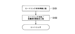
- FIG. 7 is a cross-sectional enlarged explanatory view of a joining interface between a heat sink body and a metal member layer of the heat sink shown in FIG. 6. It is a flowchart explaining the manufacturing method of the heat sink which concerns on 2nd embodiment. It is a schematic explanatory drawing of the manufacturing method of the heat sink which concerns on 2nd embodiment. It is a schematic explanatory drawing of the power module provided with the board
- FIG. 1 the power module 1 using the board
- the power module 1 includes a power module substrate 30 with a heat sink, and a semiconductor element 3 bonded to one surface (the upper surface in FIG. 1) of the power module substrate 30 with a heat sink via a solder layer 2.
- the power module substrate 30 with a heat sink includes a power module substrate 10 and a heat sink 31 bonded to the power module substrate 10.
- the power module substrate 10 is disposed on the ceramic substrate 11 constituting the insulating layer, the circuit layer 12 disposed on one surface (the upper surface in FIG. 1) of the ceramic substrate 11, and the other surface of the ceramic substrate 11. And a metal layer 13 provided.
- the ceramic substrate 11 is made of ceramics such as Si 3 N 4 (silicon nitride), AlN (aluminum nitride), and Al 2 O 3 (alumina) that are excellent in insulation and heat dissipation.
- the ceramic member 11 is made of AlN (aluminum nitride) that is particularly excellent in heat dissipation.
- the thickness of the ceramic substrate 11 is set within a range of 0.2 to 1.5 mm, for example, and is set to 0.635 mm in the present embodiment.
- the circuit layer 12 is formed by joining an aluminum plate 22 made of aluminum or an aluminum alloy to one surface of the ceramic substrate 11.
- the circuit layer 12 is formed by joining an aluminum (2N aluminum) rolled plate (aluminum plate 22) having a purity of 99% by mass or more to the ceramic substrate 11.
- the thickness of the aluminum plate 22 used as the circuit layer 12 is set in the range of 0.1 mm or more and 1.0 mm or less, and is set to 0.6 mm in this embodiment.
- the metal layer 13 is laminated on the Al layer 13A disposed on the other surface of the ceramic substrate 11 and on the surface of the Al layer 13A opposite to the surface to which the ceramic substrate 11 is bonded.
- Cu layer 13B As shown in FIG. 4, the Al layer 13 ⁇ / b> A is formed by bonding an aluminum plate 23 ⁇ / b> A made of aluminum or an aluminum alloy to the other surface of the ceramic substrate 11.
- the Al layer 13A is formed by joining an aluminum (2N aluminum) rolled plate (aluminum plate 23A) having a purity of 99% by mass or more to the ceramic substrate 11.
- the thickness of the aluminum plate 23A to be joined is set within a range of 0.1 mm or more and 3.0 mm or less, and is set to 0.6 mm in this embodiment.
- the Cu layer 13B is formed by bonding a copper plate 23B made of copper or a copper alloy to the other surface of the Al layer 13A.
- the Cu layer 13B is formed by bonding an oxygen-free copper rolled plate (copper plate 23B).
- the thickness of the copper layer 13B is set within a range of 0.1 mm to 6 mm, and is set to 1 mm in this embodiment.
- the heat sink 31 is for dissipating heat on the power module substrate 10 side, and in the present embodiment, as shown in FIG. 1, a flow path 32 through which a cooling medium flows is provided.
- the heat sink 31 is made of an aluminum alloy having a Si concentration in the range of 1 mass% to 25 mass%.
- the heat sink 31 is ADC12 (which is an aluminum alloy for die casting defined in JIS H 2118: 2006).
- the solidus temperature is 515 ° C.).
- the ADC 12 is an aluminum alloy containing Cu in a range of 1.5 mass% to 3.5 mass% and Si in a range of 9.6 mass% to 12.0 mass%.
- the Si concentration of the aluminum alloy is preferably 5 mass% or more and 20 mass% or less, more preferably 7 mass% or more and 13 mass% or less, but is not limited thereto.
- the heat sink 31 and the metal layer 13 are solid phase diffusion bonded.
- a compound layer 38 containing Al and Cu is formed at the bonding interface between the metal layer 13 (Cu layer 13 ⁇ / b> B) and the heat sink 31.
- the compound layer 38 is formed by mutual diffusion of Al atoms of the heat sink 31 and Cu atoms of the Cu layer 13B.
- the compound layer 38 has a concentration gradient in which the Al atom concentration gradually decreases and the Cu atom concentration increases as the heat sink 31 moves toward the Cu layer 13B.
- the compound layer 38 is composed of an intermetallic compound composed of Cu and Al.
- the compound layer 38 has a structure in which a plurality of intermetallic compounds are stacked along the bonding interface.
- the thickness of the compound layer 38 is set in the range of 1 ⁇ m to 80 ⁇ m, preferably in the range of 5 ⁇ m to 80 ⁇ m.
- the compound layer 38 has a structure in which three kinds of intermetallic compounds are laminated, and in order from the heat sink 31 side to the Cu layer 13B side, at the bonding interface between the heat sink 31 and the Cu layer 13B.
- the ⁇ phase and the ⁇ 2 phase are laminated, and at least one of the ⁇ 2 phase, the ⁇ phase, and the ⁇ 2 phase is laminated.
- oxide is dispersed in layers along the bonding interface at the bonding interface between the compound layer 38 and the Cu layer 13B.
- this oxide is an aluminum oxide such as alumina (Al 2 O 3 ).
- the oxide is dispersed in a state of being divided at the interface between the compound layer 38 and the Cu layer 13B, and there is a region where the compound layer 38 and the Cu layer 13B are in direct contact.
- the oxide is dispersed in layers within at least one of the ⁇ phase, ⁇ 2 phase, or ⁇ 2 phase, ⁇ phase, and ⁇ 2 phase.
- an Mg enriched layer 40 having an Mg concentration of 3 mass% or more is formed inside the compound layer 38.
- the thickness of the Mg enriched layer 40 is 1 ⁇ m. It is within the range of 30 ⁇ m or less.
- the Mg concentration of the Mg enriched layer 40 is preferably 5 mass% or more and 15 mass% or less, more preferably 7 mass% or more and 9 mass% or less, but is not limited thereto.
- an aluminum plate 22 to be the circuit layer 12 is laminated on one surface of the ceramic substrate 11 with an Al—Si brazing material foil 26 interposed therebetween. Further, an aluminum plate 23A to be the Al layer 13A is laminated on the other surface of the ceramic substrate 11 with an Al—Si based brazing material foil 26 interposed therebetween.
- an Al-8 mass% Si alloy foil having a thickness of 10 ⁇ m is used as the Al—Si brazing material foil 26.
- circuit layer and Al layer forming step S02 Then, the aluminum plate 22 and the ceramic substrate 11 are joined by placing and heating in a vacuum heating furnace under pressure in the laminating direction (pressure 1 to 35 kgf / cm 2 (0.10 to 3.43 MPa)). The circuit layer 12 is formed. Further, the ceramic substrate 11 and the aluminum plate 23A are joined to form the Al layer 13A.
- the pressure in the vacuum heating furnace is set in the range of 10 ⁇ 6 Pa to 10 ⁇ 3 Pa
- the heating temperature is set to 600 ° C. to 650 ° C.
- the holding time is set in the range of 30 minutes to 180 minutes. It is preferable.
- a copper plate 23B to be the Cu layer 13B is laminated on the other surface side of the Al layer 13A.
- the Al layer 13A and the copper plate 23B are solid-phase diffused by placing them in a vacuum heating furnace under pressure in the stacking direction (pressure 3 to 35 kgf / cm 2 (0.29 to 3.43 MPa)).
- the metal layer 13 is formed by bonding.
- the pressure in the vacuum heating furnace is set within the range of 10 ⁇ 6 Pa to 10 ⁇ 3 Pa
- the heating temperature is set to 400 ° C. to 548 ° C.
- the holding time is set within the range of 5 minutes to 240 minutes. It is preferable.
- each surface of the Al layer 13A and the copper plate 23B to be solid-phase diffusion bonded is previously smoothed by removing scratches on the surfaces.
- Heat sink preparation step S04 Next, a heat sink 31 to be joined is prepared.
- the Mg concentration in the region 31 ⁇ / b> A from the joint surface of the heat sink 31 joined to the metal layer 13 (Cu layer 13 ⁇ / b> B) to 50 ⁇ m in the depth direction is 0.3 mass% to 15 mass% within the range of
- a Mg foil 41 having a thickness of 2 ⁇ m or more and 25 ⁇ m or less is disposed on a joint surface of the heat sink 31 to be joined to the metal layer 13 (Cu layer 13B), and a heat treatment furnace 45 is provided.
- Mg is diffused to the heat sink 31 side by performing heat treatment under conditions of temperature: 420 ° C. or higher and 500 ° C. or lower and holding time: 30 min or longer and 240 min or shorter.
- the Mg concentration in 31A is in the range of 0.3 mass% to 15 mass%.
- the furnace atmosphere of the heat treatment furnace 45 during this heat treatment is preferably, for example, a nitrogen atmosphere or a vacuum atmosphere.
- the heat treatment is preferably performed under conditions of temperature: 450 ° C. or higher and 480 ° C. or lower and holding time: 60 min or longer and 120 min or shorter, but is not limited thereto.
- various foils containing Mg such as Al—Mg foil and Al—Mg—Si foil can be used.
- Mg other than the foil can be diffused by arranging Mg on the joint surface by sputtering or the like and performing a heat treatment.
- the Mg concentration in the region 31A from the joint surface to the depth direction of 50 ⁇ m exceeds 15 mass%, the Mg concentration ranges from 0.3 mass% to 15 mass% by polishing or cutting from the joint surface in the depth direction. It can also be inside.
- the Mg concentration in the region 31A is preferably 2 mass% or more and 10.8 mass% or less, more preferably 4.9 mass% or more and 8.3 mass% or less, but is not limited thereto.
- Metal layer / heat sink bonding step S05 Next, the metal layer 13 (Cu layer 13B) and the heat sink 31 are stacked and pressurized in the stacking direction (pressure 5 to 35 kgf / cm 2 (0.49 to 3.43 MPa)) in a vacuum heating furnace.
- the metal layer 13 (Cu layer 13B) and the heat sink 31 are solid-phase diffusion bonded by arranging and heating.
- each joining surface of the metal layer 13 (Cu layer 13 ⁇ / b> B) and the heat sink 31 to be solid phase diffusion bonded is previously smoothed by removing scratches on the surfaces.
- the pressure during the pressurization is more preferably 8 to 20 kgf / cm 2 (0.78 to 1.96 MPa), but is not limited thereto.
- the pressure in the vacuum heating furnace is in the range of 10 ⁇ 6 Pa to 10 ⁇ 3 Pa
- the heating temperature is 400 ° C. to 520 ° C.
- the holding time is in the range of 0.25 hour to 3 hours. It is preferably set.
- the pressure in the vacuum heating furnace is set in the range of 10 ⁇ 5 Pa to 10 ⁇ 4 Pa
- the heating temperature is set to 480 ° C. to 510 ° C.
- the holding time is set in the range of 0.5 hours to 2 hours.
- Cu atoms in the Cu layer 13B diffuse toward the heat sink 31 to form the compound layer 38 as shown in FIG. A concentrated layer 40 is formed. In this way, the power module substrate with heat sink 30 according to the present embodiment is manufactured.
- semiconductor element bonding step S06 Next, the semiconductor element 3 is stacked on one surface (front surface) of the circuit layer 12 via the solder material 2 and soldered in a reduction furnace. As described above, the power module 1 according to the present embodiment is manufactured.
- the heat sink 31 is composed of an aluminum alloy having a Si concentration in the range of 1 mass% to 25 mass%. Specifically, it is composed of ADC12 (Si concentration: 9.6 mass% or more and 12.0 mass% or less), which is an aluminum alloy for die casting defined in JIS H 2118: 2006, and thus has a complicated flow path 32.
- the heat sink 31 having a structure can be configured, and the heat dissipation performance can be improved.
- a compound layer 38 made of an intermetallic compound of Al and Cu is formed at the bonding interface between the heat sink 31 and the metal layer 13 (Cu layer 13B).
- An Mg enriched layer 40 having an Mg concentration of 3 mass% or more is formed, and the thickness of the Mg enriched layer 40 is in the range of 1 ⁇ m to 30 ⁇ m.
- the diffusion movement of Cu atoms in the layer 13 (Cu layer 13B) is hindered, and the generation of Kirkendall void can be suppressed.
- Cu atoms of the metal layer 13 (Cu layer 13B) can be sufficiently diffused to the heat sink 31 side, and the heat sink 31 and the metal layer 13 (Cu layer 13B) can be reliably solid-phase diffusion bonded. Therefore, in this power module substrate 30 with a heat sink, the thermal resistance in the stacking direction is low, and it is possible to suppress the deterioration of the heat dissipation characteristics.
- the thickness of the Mg concentrated layer 40 is set in the range of 1 ⁇ m to 30 ⁇ m.
- the lower limit of the thickness of the Mg concentrated layer 40 is preferably 7 ⁇ m or more, and more preferably 10 ⁇ m or more.
- the upper limit of the thickness of the Mg concentrated layer 40 is preferably 25 ⁇ m or less, and preferably 20 ⁇ m or less. Is more preferable.
- a compound layer 38 made of a compound layer of Cu and Al is formed at the bonding interface between the metal layer 13 (Cu layer 13B) and the heat sink 31, and the compound layer 38 is composed of a plurality of metals. Since the intermetallic compound is laminated along the bonding interface, the brittle intermetallic compound can be prevented from growing greatly. Further, the volume variation inside the compound layer 38 is reduced, and internal strain is suppressed. In the present embodiment, since oxides are dispersed in layers along the bonding interface between the Cu layer 13 ⁇ / b> B and the compound layer 38, the oxide formed on the bonding surface of the heat sink 31. The film is surely destroyed, the mutual diffusion of Cu and Al is sufficiently advanced, and the Cu layer 13B and the heat sink 31 are reliably bonded.
- the bonding to be bonded to the metal layer 13 (Cu layer 13B) in the heat sink 31 in the heat sink preparation step S04, as the heat sink 31 before bonding, the bonding to be bonded to the metal layer 13 (Cu layer 13B) in the heat sink 31. Since the Mg concentration in the region 31A from the surface to the depth direction of 50 ⁇ m in the range of 0.3 mass% to 15 mass% is prepared, in the metal layer / heat sink joining step S05, When the metal layer 13 (Cu layer 13B) is solid-phase diffusion bonded, Cu atoms in the Cu layer 13B can be prevented from diffusing and moving more than necessary, and the generation of Kirkendall voids can be suppressed. Therefore, it is possible to manufacture the power module substrate 30 with a heat sink having a low thermal resistance in the stacking direction and excellent heat dissipation characteristics.
- Mg foil 41 having a thickness of 2 ⁇ m or more and 25 ⁇ m or less is disposed on a joint surface of the heat sink 31 to be joined with the metal layer 13 (Cu layer 13B), and temperature: 420 ° C. or more and 500 ° C. or less. Holding time: By performing heat treatment under conditions of 30 min to 240 min, Mg is diffused to the heat sink 31 side, and the Mg concentration in the region 31A from the bonding surface to 50 ⁇ m in the depth direction is 0.3 mass% to 15 mass%. Therefore, Mg can be disposed on the bonding surface with the metal layer 13 (Cu layer 13B), and the Mg concentrated layer 40 can be formed in the subsequent metal layer / heat sink bonding step S05. It becomes.
- a gap may be formed at the bonding interface, but in this embodiment, the Cu layer 13B (copper plate 23B) and the surface to which the heat sink 31 is bonded. Since the solid-phase diffusion bonding is performed after the surface scratches have been removed and smoothed in advance, the formation of a gap at the bonding interface can be suppressed, and solid-phase diffusion bonding can be reliably performed.
- FIG. 6 shows a heat sink 101 according to the second embodiment of the present invention.
- the heat sink 101 includes a heat sink body 110 and a metal member layer 117 made of copper, nickel, or silver laminated on one surface of the heat sink body 110 (upper side in FIG. 6).
- the metal member layer 117 is configured by joining a metal plate 127 made of an oxygen-free copper rolled plate to the heat sink body 110, as shown in FIG.
- the heat sink body 110 is provided with a flow path 111 through which a cooling medium flows.
- the heat sink body 110 is made of an aluminum alloy having a Si concentration in the range of 1 mass% to 25 mass%. Specifically, Si is in the range of 9.6 mass% to 12 mass%, and Mg is contained. It is comprised with the aluminum alloy contained within the range of 0.3 mass% or more and 15 mass% or less.
- the Si concentration of the aluminum alloy is preferably 5 mass% or more and 20 mass% or less, more preferably 7 mass% or more and 13 mass% or less, but is not limited thereto.
- the heat sink body 110 and the metal member layer 117 are solid phase diffusion bonded.
- a compound layer 138 is formed at the bonding interface between the heat sink body 110 and the metal member layer 117 as shown in FIG.
- the compound layer 138 is formed by mutual diffusion of Al atoms in the heat sink body 110 and Cu atoms in the metal member layer 117.
- the compound layer 138 has a concentration gradient in which the Al atom concentration gradually decreases and the Cu atom concentration increases as the heat sink body 110 moves toward the metal member layer 117.
- the compound layer 138 is composed of an intermetallic compound composed of Cu and Al.
- the compound layer 138 has a structure in which a plurality of intermetallic compounds are stacked along the bonding interface.
- the thickness of the compound layer 138 is set in a range of 1 ⁇ m to 80 ⁇ m, preferably in a range of 5 ⁇ m to 80 ⁇ m.
- the compound layer 138 has a structure in which three kinds of intermetallic compounds are laminated, and the heat sink body 110 and the metal member layer are sequentially arranged from the heat sink body 110 side to the metal member layer 117 side.
- a ⁇ phase and a ⁇ 2 phase are laminated along a bonding interface with 117, and at least one of a ⁇ 2 phase, a ⁇ phase, and a ⁇ 2 phase is laminated.
- oxide is dispersed in layers along the bonding interface at the bonding interface between the compound layer 138 and the metal member layer 117.
- this oxide is an aluminum oxide such as alumina (Al 2 O 3 ).
- Al 2 O 3 aluminum oxide
- the oxide is dispersed in a state of being divided at the interface between the compound layer 138 and the metal member layer 117, and there is a region where the compound layer 138 and the metal member layer 117 are in direct contact with each other.
- the oxide is dispersed in layers within at least one of the ⁇ phase, the ⁇ 2 phase, or the ⁇ 2 phase, the ⁇ phase, and the ⁇ 2 phase.
- an Mg concentrated layer 140 in which the Mg concentration is 3 mass% or more is formed inside the compound layer 138, and the thickness of the Mg concentrated layer 140 is 1 ⁇ m. It is within the range of 30 ⁇ m or less.
- the Mg concentration of the Mg enriched layer 140 is preferably 5 mass% or more and 15 mass% or less, more preferably 7 mass% or more and 9 mass% or less, but is not limited thereto.
- the thickness of the Mg concentrated layer 140 is preferably 3 ⁇ m or more and 25 ⁇ m or less, more preferably 5 ⁇ m or more and 20 ⁇ m or less, but is not limited thereto.
- the heat sink body 110 to be joined is prepared.
- the Mg concentration in a region from the joint surface joined to the metal member layer 117 to 50 ⁇ m in the depth direction in the heat sink main body 110 is set in the range of 0.3 mass% to 15 mass%.
- the entire heat sink body 110 contains Mg within a range of 0.3 mass% to 15 mass%.
- the Mg concentration in the region of the heat sink body 110 in the depth direction from the joint surface joined to the metal member layer 117 to 50 ⁇ m is preferably 2 mass% to 10.8 mass%, more preferably 4.9 mass% to 8. Although it is 3 mass% or less, it is not limited to this.
- the heat sink body 110 and the metal plate 127 to be the metal member layer 117 are laminated, and pressure is applied in the laminating direction (pressure 1 to 35 kgf / cm 2 (0.10 to 3.43 MPa).
- pressure is applied in the laminating direction (pressure 1 to 35 kgf / cm 2 (0.10 to 3.43 MPa).
- the metal plate 127 and the heat sink body 110 are solid-phase diffusion bonded by being placed in a vacuum heating furnace and heated.
- each joining surface of the metal plate 127 and the heat sink body 110 to be solid phase diffusion bonded is previously smoothed by removing scratches on the surfaces.
- the pressure during the pressurization is more preferably 8 to 20 kgf / cm 2 (0.78 to 1.96 MPa), but is not limited thereto.
- the pressure in the vacuum heating furnace is in the range of 10 ⁇ 6 Pa to 10 ⁇ 3 Pa
- the heating temperature is 400 ° C. to 520 ° C.
- the holding time is in the range of 0.25 hour to 3 hours. It is preferably set.
- the pressure in the vacuum heating furnace is set in the range of 10 ⁇ 5 Pa to 10 ⁇ 4 Pa
- the heating temperature is set to 480 ° C. to 510 ° C.
- the holding time is set in the range of 0.5 hours to 2 hours.
- Cu atoms in the metal plate 127 diffuse toward the heat sink body 110, forming a compound layer 138 as shown in FIG. Then, the Mg concentrated layer 140 is formed.
- the heat sink 101 which is this embodiment is manufactured.
- the metal member layer 117 is formed by joining the metal plate 127 made of an oxygen-free copper rolled plate to one surface side of the heat sink body 110. Since it is formed, heat can be spread in the surface direction by the metal member layer 117, and the heat dissipation characteristics can be greatly improved. In addition, other members and the heat sink 101 can be favorably bonded using solder or the like.
- the heat sink body 110 is made of an aluminum alloy having a Si concentration in the range of 1 mass% to 25 mass%. Specifically, Si is in the range of 9.6 mass% to 12 mass%, Mg Therefore, the heat sink body 110 having a complicated structure having a flow path and the like can be configured since the aluminum alloy is included in the range of 0.3 mass% to 15 mass%.
- a compound layer 138 is formed at the bonding interface between the heat sink body 110 and the metal member layer 117 as shown in FIG. 7, and the inside of the compound layer 138 is shown in FIG.
- the Mg concentration layer 140 in which the Mg concentration is 3 mass% or more is formed, and the thickness of the Mg concentration layer 140 is in the range of 1 ⁇ m to 30 ⁇ m.
- the layer 140 prevents the diffusion movement of Cu atoms in the metal member layer 117, and the generation of Kirkendall void can be suppressed. Therefore, the thermal resistance in the stacking direction is low, and the heat dissipation characteristics are excellent.
- the Mg concentrated layer 140 has a thickness of 30 ⁇ m or less, the diffusion of Cu atoms is not restricted more than necessary, and the heat sink body 110 and the metal member layer 117 are securely solid-phase diffusion bonded. be able to.
- the bonding interface between the metal member layer 117 and the heat sink body 110 has the same configuration as the bonding interface between the Cu layer 13B and the heat sink 31 in the first embodiment. It is possible to achieve the same function and effect.
- the thickness of the Ni layer is preferably 1 ⁇ m or more and 30 ⁇ m or less. If the thickness of the Ni layer is less than 1 ⁇ m, the effect of improving the reliability of bonding with other members may be lost. If the thickness exceeds 30 ⁇ m, the Ni layer becomes a thermal resistor and heat can be transferred efficiently. There is a risk of disappearing.
- the bonding temperature is set to 400 ° C. or more and 520 ° C. or less for the solid phase diffusion bonding of the Al layer and Ni, but other conditions are the same as in the above-described embodiment. It can be formed under the following conditions.
- the silver oxide of the silver oxide paste is reduced. Since the silver reduced by the agent and the Ag layer to be bonded are bonded between the same kind of metals, the bonding reliability can be improved. Furthermore, since an Ag layer having a good thermal conductivity is formed, heat can be spread efficiently by spreading in the surface direction.
- the thickness of the Ag layer is preferably 1 ⁇ m or more and 20 ⁇ m or less. If the thickness of the Ag layer is less than 1 ⁇ m, the effect of improving the reliability of bonding with other members may be lost.
- the bonding temperature is set to 400 ° C. or more and 520 ° C. or less, but the other conditions are the same as those in the above embodiment. Can be formed.
- the metal layer 13 has been described as having the Al layer 13A and the Cu layer 13B.
- the present invention is not limited to this, and as shown in FIG. Or you may comprise with a copper alloy.
- a copper plate is joined to the other surface (lower side in FIG. 10) of the ceramic substrate 11 by the DBC method, the active metal brazing method, or the like.
- a metal layer 213 is formed.
- the metal layer 213 and the heat sink 31 are solid phase diffusion bonded.
- the circuit layer 212 is also made of copper or a copper alloy.
- a power module 201 shown in FIG. 10 includes a power module substrate 230 with a heat sink, and a semiconductor element 3 bonded to one surface (the upper surface in FIG. 10) of the power module substrate 230 with a heat sink via a solder layer 2. It is equipped with.
- the circuit layer is described as being formed by bonding an aluminum plate having a purity of 99% by mass, but is not limited thereto, and pure aluminum having a purity of 99.99% by mass or more, It may be composed of other metals such as aluminum or aluminum alloy, copper or copper alloy.
- the circuit layer may have a two-layer structure of an Al layer and a Cu layer. The same applies to the power module substrate 210 shown in FIG.
- the metal layer 13 (Cu layer 13B) and the heat sink 31 are laminated, placed in a vacuum heating furnace in a state of being pressurized in the lamination direction, and heated.
- the heat sink main body / metal member layer joining step S102 of the second embodiment the heat sink main body 110 and the metal plate 127 to be the metal member layer 117 are stacked and pressurized in the stacking direction (pressure 5 to 35 kgf /
- the present invention is not limited to this, and as shown in FIG.
- an electric heating method is used. It may be.
- an aluminum alloy member 301 and a metal member 302 are laminated, and these laminated bodies are laminated by a pair of electrodes 312 and 312 via carbon plates 311 and 311. While pressing in the direction, the aluminum alloy member 301 and the metal member 302 are energized. Then, the carbon plates 311 and 311 and the aluminum alloy member 301 and the metal member 302 are heated by Joule heat, and the aluminum alloy member 301 and the metal member 302 are solid-phase diffusion bonded.
- the rate of temperature increase can be made relatively fast, for example, 30 to 100 ° C./min, and the solid phase can be obtained in a short time. Diffusion bonding can be performed. Thereby, the influence of the oxidation of the bonding surface is small, and for example, bonding can be performed even in an air atmosphere. Further, depending on the resistance value and specific heat of the aluminum alloy member 301 and the metal member 302, it is possible to join the aluminum alloy member 301 and the metal member 302 in a state where a temperature difference is generated, thereby reducing the difference in thermal expansion, Thermal stress can also be reduced.
- the pressure load applied by the pair of electrodes 312 and 312 is set to be within a range of 30 kgf / cm 2 to 100 kgf / cm 2 (2.94 MPa to 9.8 MPa). preferable.
- the pressure load is more preferably 50 kgf / cm 2 or more and 80 kgf / cm 2 or less (4.90 MPa or more and 7.85 MPa or less), but is not limited thereto.
- the surface roughness of the aluminum alloy member 301 and the metal member 302 is 0.3 ⁇ m or more and 0.6 ⁇ m or less in terms of arithmetic average roughness Ra, or 1.
- the surface roughness of the bonding surface is small, but in the case of the electric heating method, if the surface roughness of the bonding surface is too small, the interface contact resistance decreases, and the bonding interface Since it becomes difficult to heat locally, it is preferable to be within the above range.
- the ceramic substrate 11 is an insulator, for example, a jig made of carbon, etc. Therefore, it is necessary to short-circuit the carbon plates 311 and 311.
- the joining conditions are the same as the joining of the aluminum member 301 and the copper member 302 described above.
- the surface roughness of the metal layer 13 (Cu layer 13B) and the heat sink 31 is the same as that of the aluminum member 301 and the copper member 302 described above.
- Example 11-15 an aluminum alloy plate and a metal plate were joined by solid phase diffusion bonding by the electric heating method shown in FIG. Note that the pressure load on the electrode was 15 kgf / cm 2 (1.47 MPa), the heating temperature (copper plate temperature) was 510 ° C., the holding time at the heating temperature was 5 min, and the heating rate was 80 ° C./min.
- the bonding atmosphere was an air atmosphere.
- the thickness of the Mg enriched layer is determined by measuring the area of the region where the Mg concentration is 3 mass% or more from the Mg mapping image by EPMA (electron beam microanalyzer) at the joint interface between the aluminum alloy plate and the metal plate, The thickness was obtained by dividing by the above dimensions, and the average of the five fields of view was the thickness of the Mg concentrated layer. The measurement was performed at a magnification of 2000 times, and the measurement was performed in a range of 50 ⁇ m in the stacking direction centering on the contact surface between the aluminum alloy plate and the metal plate.
- Heat cycle test Next, a heat cycle test was performed on the joined body thus manufactured.
- the thermal resistance and bonding rate in the stacking direction of the bonded body before the heat cycle test, and the thermal resistance and bonding rate in the stacking direction of the bonded body after the heat cycle test were evaluated as follows.
- Bonding rate evaluation The joining rate of the joined part between the aluminum plate and the metal plate of the joined body was evaluated using an ultrasonic flaw detector and calculated from the following formula.
- the initial bonding area is the area to be bonded before bonding, that is, the area of the aluminum plate. Since peeling is indicated by a white part in the ultrasonic flaw detection image, the area of the white part is defined as a peeling area.
- Bonding rate (%) ⁇ (initial bonding area) ⁇ (peeling area) ⁇ / (initial bonding area) ⁇ 100
- Comparative Example 1 in which the Mg concentrated layer was not formed, it was confirmed that the thermal resistance was higher than that of the inventive example. Moreover, when Comparative Example 4 using nickel as the metal plate was compared with Invention Examples 9 and 14, it was confirmed that the thermal resistance of Comparative Example 4 was increased. Similarly, when Comparative Example 5 using silver as a metal plate was compared with Invention Examples 10 and 15, it was confirmed that the thermal resistance of Comparative Example 5 was increased. These are presumed to be due to the formation of Kirkendall void.
- Comparative Example 2 in which the thickness of the Mg concentrated layer exceeded the upper limit of the present invention, the bonding rate was low and the thermal resistance was large. It is presumed that the Mg enriched layer is formed thick, so that the diffusion of the metal element of the metal plate is suppressed. Further, in Comparative Example 3 where the thickness of the Mg concentrated layer is thinner than the lower limit of the present invention, it was confirmed that the resistance was increased as in Comparative Example 1. It is presumed that the generation of Kirkendall voids could not be sufficiently suppressed.
- the thermal resistance is smaller than that of the comparative example, and the joining rate is sufficiently high. confirmed. It is presumed that by forming the Mg concentrated layer having an appropriate thickness, the diffusion of the metal elements constituting the metal plate is suppressed and the generation of Kirkendall voids is suppressed. Further, in Invention Examples 11-15 to which the energization heating method was applied, the aluminum alloy plate and the metal plate were satisfactorily joined even when they were joined in the air. Furthermore, it was confirmed that an increase in thermal resistance and a decrease in bonding rate after the heat cycle test were hardly observed, and a bonded body with high bonding reliability was obtained.
- an aluminum alloy member made of an aluminum alloy containing a relatively large amount of Si and a metal member made of copper, nickel, or silver are satisfactorily bonded, and the thermal resistance in the stacking direction is low. It was confirmed that a joined body could be obtained.
- an aluminum alloy member made of an aluminum alloy containing a relatively large amount of Si and a metal member made of copper, nickel, or silver are well bonded, and a bonded body having a low thermal resistance in the stacking direction, and this bonding It is possible to provide a power module substrate with a heat sink and a heat sink having a body, a method for manufacturing a joined body, a method for manufacturing a power module substrate with a heat sink, and a method for manufacturing a heat sink.
Abstract
本発明の接合体は、アルミニウム合金からなるアルミニウム合金部材と、銅、ニッケル、又は銀からなる金属部材とが接合された接合体であって、アルミニウム合金部材は、Si濃度が1mass%以上25mass%以下の範囲内とされたアルミニウム合金で構成され、アルミニウム合金部材と金属部材とが固相拡散接合されており、アルミニウム合金部材と金属部材との接合界面に、アルミニウム合金部材のAlと金属部材の金属元素とが拡散して形成された化合物層を備え、この化合物層の内部に、Mgの濃度が3mass%以上とされたMg濃化層が形成されており、前記Mg濃化層の厚さが1μm以上30μm以下の範囲内とされている。
Description
この発明は、アルミニウム合金部材と、銅、ニッケル、又は銀からなる金属部材とが接合されてなる接合体、絶縁層の一方の面に回路層が形成されたパワーモジュール用基板にヒートシンクが接合されたヒートシンク付パワーモジュール用基板、ヒートシンク本体に金属部材層が形成されたヒートシンク、接合体の製造方法、ヒートシンク付パワーモジュール用基板の製造方法、及び、ヒートシンクの製造方法に関する。
本願は、2015年4月16日に、日本に出願された特願2015-084030号、2016年2月24日に、日本に出願された特願2016-033202号に基づき優先権を主張し、その内容をここに援用する。
本願は、2015年4月16日に、日本に出願された特願2015-084030号、2016年2月24日に、日本に出願された特願2016-033202号に基づき優先権を主張し、その内容をここに援用する。
LEDやパワーモジュール等の半導体装置においては、導電材料からなる回路層の上に半導体素子が接合された構造を備えている。
風力発電、電気自動車、ハイブリッド自動車等を制御するために用いられる大電力制御用のパワー半導体素子においては、発熱量が多い。そのため、大電力制御用のパワー半導体素子を搭載する基板としては、例えばAlN(窒化アルミニウム)、Al2O3(アルミナ)などからなるセラミックス基板と、このセラミックス基板の一方の面に導電性の優れた金属板を接合して形成した回路層と、を備えたパワーモジュール用基板が、従来から広く用いられている。なお、パワージュール用基板としては、セラミックス基板の他方の面に金属層を形成したものも提供されている。
風力発電、電気自動車、ハイブリッド自動車等を制御するために用いられる大電力制御用のパワー半導体素子においては、発熱量が多い。そのため、大電力制御用のパワー半導体素子を搭載する基板としては、例えばAlN(窒化アルミニウム)、Al2O3(アルミナ)などからなるセラミックス基板と、このセラミックス基板の一方の面に導電性の優れた金属板を接合して形成した回路層と、を備えたパワーモジュール用基板が、従来から広く用いられている。なお、パワージュール用基板としては、セラミックス基板の他方の面に金属層を形成したものも提供されている。
例えば、特許文献1に示すパワーモジュールにおいては、セラミックス基板の一方の面及び他方の面にAlからなる回路層及び金属層が形成されたパワーモジュール用基板と、この回路層上にはんだ材を介して接合された半導体素子と、を備えた構造とされている。
パワーモジュール用基板の金属層側には、ヒートシンクが接合されており、半導体素子からパワーモジュール用基板側に伝達された熱を、ヒートシンクを介して外部へ放散する構成とされている。
パワーモジュール用基板の金属層側には、ヒートシンクが接合されており、半導体素子からパワーモジュール用基板側に伝達された熱を、ヒートシンクを介して外部へ放散する構成とされている。
ところで、特許文献1に記載されたパワーモジュールのように、回路層及び金属層をAlで構成した場合には、表面にAlの酸化皮膜が形成されるため、はんだ材によって半導体素子やヒートシンクを接合することができない。
そこで、従来、例えば特許文献2に開示されているように、回路層及び金属層の表面に無電解めっき等によってNiめっき膜を形成した上で、半導体素子やヒートシンクをはんだ接合している。
また、特許文献3には、はんだ材の代替として、酸化銀粒子と有機物からなる還元剤とを含む酸化銀ペーストを用いて、回路層と半導体素子、金属層とヒートシンクを接合する技術が提案されている。
そこで、従来、例えば特許文献2に開示されているように、回路層及び金属層の表面に無電解めっき等によってNiめっき膜を形成した上で、半導体素子やヒートシンクをはんだ接合している。
また、特許文献3には、はんだ材の代替として、酸化銀粒子と有機物からなる還元剤とを含む酸化銀ペーストを用いて、回路層と半導体素子、金属層とヒートシンクを接合する技術が提案されている。
しかしながら、特許文献2に記載されたように、回路層及び金属層表面にNiめっき膜を形成したパワーモジュール用基板においては、半導体素子及びヒートシンクを接合するまでの過程においてNiめっき膜の表面が酸化等によって劣化し、はんだ材を介して接合した半導体素子及びヒートシンクとの接合信頼性が低下するおそれがあった。ここで、ヒートシンクと金属層との接合が不十分であると、熱抵抗が上昇し、放熱特性が低下するおそれがあった。また、Niめっき工程では、不要な領域にNiめっきが形成されて電食等のトラブルが発生しないように、マスキング処理を行うことがある。このように、マスキング処理をした上でめっき処理をする場合、回路層表面及び金属層表面にNiめっき膜を形成する工程に多大な労力が必要となり、パワーモジュールの製造コストが大幅に増加してしまうといった問題があった。
また、特許文献3に記載されたように、酸化銀ペーストを用いて回路層と半導体素子、金属層とヒートシンクを接合する場合には、Alと酸化銀ペーストの焼成体との接合性が悪いために、予め回路層表面及び金属層表面にAg下地層を形成する必要があった。Ag下地層をめっきにより形成する場合には、Niめっきと同様に多大な労力が必要となるといった問題があった。
そこで、特許文献4には、回路層及び金属層をAl層とCu層の積層構造としたパワーモジュール用基板が提案されている。このパワーモジュール用基板においては、回路層及び金属層の表面にはCu層が配置されるため、はんだ材を用いて半導体素子及びヒートシンクを良好に接合することができる。このため、積層方向の熱抵抗が小さくなり、半導体素子から発生した熱をヒートシンク側へと効率良く伝達することが可能となる。
また、特許文献5には、金属層及びヒートシンクの一方がアルミニウム又はアルミニウム合金で構成され、他方が銅又は銅合金で構成されており、これら前記金属層と前記ヒートシンクとが固相拡散接合されたヒートシンク付パワーモジュール用基板が提案されている。このヒートシンク付パワーモジュール用基板においては、金属層とヒートシンクとが固相拡散接合されているので、熱抵抗が小さく、放熱特性に優れている。
ところで、内部に冷却媒体の流路等が形成された複雑な構造のヒートシンクにおいては、Siを比較的多く含むアルミニウム鋳物合金を用いて製造されることがある。
ここで、Siを比較的多く含むアルミニウム鋳物合金からなるアルミニウム合金部材と、銅、ニッケル、又は銀からなる金属部材とを、特許文献5に記載されたように、固相拡散接合した場合には、接合界面近傍に相互拡散の不均衡によって生じるカーケンダルボイドが多数発生することが確認された。このようなカーケンダルボイドがパワーモジュール用基板とヒートシンクとの間に存在すると、熱抵抗が上昇し、放熱特性が低下してしまうといった問題があった。
ここで、Siを比較的多く含むアルミニウム鋳物合金からなるアルミニウム合金部材と、銅、ニッケル、又は銀からなる金属部材とを、特許文献5に記載されたように、固相拡散接合した場合には、接合界面近傍に相互拡散の不均衡によって生じるカーケンダルボイドが多数発生することが確認された。このようなカーケンダルボイドがパワーモジュール用基板とヒートシンクとの間に存在すると、熱抵抗が上昇し、放熱特性が低下してしまうといった問題があった。
この発明は、前述した事情に鑑みてなされたものであって、Siを比較的多く含むアルミニウム合金からなるアルミニウム合金部材と、銅、ニッケル、又は銀からなる金属部材とが良好に接合され、積層方向の熱抵抗が低い接合体、この接合体を備えたヒートシンク付パワーモジュール用基板及びヒートシンク、及び、接合体の製造方法、ヒートシンク付パワーモジュール用基板の製造方法、ヒートシンクの製造方法を提供することを目的とする。
前述の課題を解決するために、本発明の一態様である接合体は、アルミニウム合金からなるアルミニウム合金部材と、銅、ニッケル、又は銀からなる金属部材とが接合された接合体であって、前記アルミニウム合金部材は、Si濃度が1mass%以上25mass%以下の範囲内とされたアルミニウム合金で構成され、前記アルミニウム合金部材と前記金属部材とが固相拡散接合されており、前記アルミニウム合金部材と前記金属部材との接合界面に、前記アルミニウム合金部材のAlと前記金属部材の金属元素とが拡散して形成された化合物層を備え、この化合物層の内部に、Mgの濃度が3mass%以上とされたMg濃化層が形成されており、前記Mg濃化層の厚さが1μm以上30μm以下の範囲内とされていることを特徴としている。
なお、本発明において、金属部材は、銅又は銅合金、ニッケル又はニッケル合金、もしくは銀又は銀合金で構成されている。
なお、本発明において、金属部材は、銅又は銅合金、ニッケル又はニッケル合金、もしくは銀又は銀合金で構成されている。
この構成の接合体によれば、前記アルミニウム合金部材と前記金属部材との接合界面に、前記アルミニウム合金部材のAlと前記金属部材の金属元素とが拡散して形成された化合物層を備え、この化合物層の内部に、Mgの濃度が3mass%以上とされたMg濃化層が形成されており、前記Mg濃化層の厚さが1μm以上30μm以下の範囲内とされているので、このMg濃化層によって金属部材を構成する金属元素の拡散移動が妨げられて、カーケンダルボイドの発生が抑制されることになり、積層方向の熱抵抗を低くすることができる。
本発明の一態様であるヒートシンク付パワーモジュール用基板は、絶縁層と、この絶縁層の一方の面に形成された回路層と、前記絶縁層の他方の面に形成された金属層と、この金属層の前記絶縁層とは反対側の面に配置されたヒートシンクと、を備えたヒートシンク付パワーモジュール用基板であって、前記金属層のうち前記ヒートシンクとの接合面は、銅、ニッケル、又は銀で構成され、前記ヒートシンクのうち前記金属層との接合面は、Si濃度が1mass%以上25mass%以下の範囲内とされたアルミニウム合金で構成され、前記ヒートシンクと前記金属層とが固相拡散接合されており、前記ヒートシンクと前記金属層との接合界面に、前記ヒートシンクのAlと前記金属層の接合面を構成する金属元素とが拡散して形成された化合物層を備え、この化合物層の内部に、Mgの濃度が3mass%以上とされたMg濃化層が形成されており、前記Mg濃化層の厚さが1μm以上30μm以下の範囲内とされていることを特徴としている。
この構成のヒートシンク付パワーモジュール用基板によれば、前記ヒートシンクと前記金属層との接合界面に、前記ヒートシンクのAlと前記金属層の接合面を構成する金属元素とが拡散して形成された化合物層を備え、この化合物層の内部に、Mgの濃度が3mass%以上とされたMg濃化層が形成されており、前記Mg濃化層の厚さが1μm以上30μm以下の範囲内とされているので、このMg濃化層によって金属層を構成する金属元素の拡散移動が妨げられて、カーケンダルボイドの発生が抑制される。このため、積層方向の熱抵抗が低く、放熱特性に特に優れている。
本発明の一態様であるヒートシンクは、ヒートシンク本体と、前記ヒートシンク本体に接合された金属部材層と、を備えたヒートシンクであって、前記金属部材層は、銅、ニッケル、又は銀からなり、前記ヒートシンク本体は、Si濃度が1mass%以上25mass%以下の範囲内とされたアルミニウム合金で構成され、前記ヒートシンク本体と前記金属部材層とが固相拡散接合されており、前記ヒートシンク本体と前記金属部材層との接合界面に、前記ヒートシンク本体のAlと前記金属部材層を構成する金属元素とが拡散して形成された化合物層を備え、この化合物層の内部に、Mgの濃度が3mass%以上とされたMg濃化層が形成されており、前記Mg濃化層の厚さが1μm以上30μm以下の範囲内とされていることを特徴としている。
この構成のヒートシンクによれば、前記ヒートシンク本体と前記金属部材層との接合界面に、前記ヒートシンク本体のAlと前記金属部材層を構成する金属元素とが拡散して形成された化合物層を備え、この化合物層の内部に、Mgの濃度が3mass%以上とされたMg濃化層が形成されており、前記Mg濃化層の厚さが1μm以上30μm以下の範囲内とされているので、この前記Mg濃化層によって金属部材層を構成する金属元素の拡散移動が妨げられて、カーケンダルボイドの発生が抑制される。このため、積層方向の熱抵抗が低く、放熱特性に特に優れている。
本発明の一態様である接合体の製造方法は、アルミニウム合金からなるアルミニウム合金部材と、銅、ニッケル、又は銀からなる金属部材とが接合されてなる接合体の製造方法であって、前記アルミニウム合金部材は、Si濃度が1mass%以上25mass%以下の範囲内とされたアルミニウム合金で構成されており、接合前の前記アルミニウム合金部材において、少なくとも前記金属部材との接合面から深さ方向に50μmまでの領域におけるMg濃度を0.3mass%以上15mass%以下の範囲内とし、このアルミニウム合金部材と前記金属部材とを固相拡散接合することを特徴としている。
この構成の接合体の製造方法によれば、接合前の前記アルミニウム合金部材において、少なくとも前記金属部材との接合面から深さ方向に50μmまでの領域におけるMg濃度を0.3mass%以上15mass%以下の範囲内としているので、固相拡散接合時に金属部材を構成する金属元素が必要以上に拡散移動することを、接合面近傍に存在するMgによって抑制することができ、カーケンダルボイドの発生を抑制することができる。
ここで、本発明の一態様である接合体の製造方法においては、前記アルミニウム合金部材と前記金属部材とを積層し、積層方向に加圧しながら通電して加熱することにより、前記アルミニウム合金部材と前記金属部材とを固相拡散接合することが好ましい。
この場合、前記アルミニウム合金部材と前記金属部材とを積層方向に加圧しながら通電加熱しているので、昇温速度を速くすることができ、比較的短時間で固相拡散接合を行うことが可能となる。これにより、例えば大気中で接合した場合でも、接合面の酸化の影響が小さく、前記アルミニウム合金部材と前記金属部材とを良好に接合することができる。
この場合、前記アルミニウム合金部材と前記金属部材とを積層方向に加圧しながら通電加熱しているので、昇温速度を速くすることができ、比較的短時間で固相拡散接合を行うことが可能となる。これにより、例えば大気中で接合した場合でも、接合面の酸化の影響が小さく、前記アルミニウム合金部材と前記金属部材とを良好に接合することができる。
本発明の一態様であるヒートシンク付パワーモジュール用基板の製造方法は、絶縁層と、この絶縁層の一方の面に形成された回路層と、前記絶縁層の他方の面に形成された金属層と、この金属層の前記絶縁層とは反対側の面に配置されたヒートシンクと、を備えたヒートシンク付パワーモジュール用基板の製造方法であって、前記金属層のうち前記ヒートシンクとの接合面は、銅、ニッケル、又は銀で構成され、前記ヒートシンクのうち前記金属層との接合面は、Si濃度が1mass%以上25mass%以下の範囲内とされたアルミニウム合金で構成されており、接合前の前記ヒートシンクにおいて、少なくとも前記金属層との接合面から深さ方向に50μmまでの領域におけるMg濃度を0.3mass%以上15mass%以下の範囲内とし、このヒートシンクと前記金属層とを固相拡散接合することを特徴としている。
この構成のヒートシンク付パワーモジュール用基板の製造方法によれば、接合前の前記ヒートシンクにおいて、少なくとも前記金属層との接合面から深さ方向に50μmまでの領域におけるMg濃度を0.3mass%以上15mass%以下の範囲内としているので、固相拡散接合時に金属層の接合面を構成する金属元素が必要以上に拡散移動することを、接合面近傍に存在するMgによって抑制することができ、カーケンダルボイドの発生を抑制することができる。
よって、積層方向における熱抵抗が低く、放熱特性に優れたヒートシンク付パワーモジュール用基板を製造することが可能となる。
よって、積層方向における熱抵抗が低く、放熱特性に優れたヒートシンク付パワーモジュール用基板を製造することが可能となる。
ここで、本発明の一態様であるヒートシンク付パワーモジュール用基板の製造方法においては、前記ヒートシンクと前記金属層とを積層し、積層方向に加圧しながら通電して加熱することにより、前記ヒートシンクと前記金属層とを固相拡散接合することが好ましい。
この場合、前記ヒートシンクと前記金属層とを積層方向に加圧しながら通電加熱しているので、昇温速度を速くすることができ、比較的短時間で固相拡散接合を行うことが可能となる。これにより、例えば大気中で接合した場合でも、接合面の酸化の影響が小さく、前記ヒートシンクと前記金属層とを良好に接合することができる。
この場合、前記ヒートシンクと前記金属層とを積層方向に加圧しながら通電加熱しているので、昇温速度を速くすることができ、比較的短時間で固相拡散接合を行うことが可能となる。これにより、例えば大気中で接合した場合でも、接合面の酸化の影響が小さく、前記ヒートシンクと前記金属層とを良好に接合することができる。
本発明の一態様であるヒートシンクの製造方法は、ヒートシンク本体と、前記ヒートシンク本体に接合された金属部材層と、を備えたヒートシンクの製造方法であって、前記金属部材層は、銅、ニッケル、又は銀からなり、前記ヒートシンク本体は、Si濃度が1mass%以上25mass%以下の範囲内とされたアルミニウム合金で構成されており、接合前の前記ヒートシンク本体において、少なくとも前記金属部材層との接合面から50μmまでの領域におけるMg濃度を0.3mass%以上15mass%以下の範囲内とし、このヒートシンク本体と前記金属部材層とを固相拡散接合することを特徴としている。
この構成のヒートシンクの製造方法によれば、接合前の前記ヒートシンク本体において、少なくとも前記金属部材層との接合面から深さ方向に50μmまでの領域におけるMg濃度を0.3mass%以上15mass%以下の範囲内としているので、固相拡散接合時に金属部材層を構成する金属元素が必要以上に拡散移動することを、接合面近傍に存在するMgによって抑制でき、カーケンダルボイドの発生を抑制することができる。
よって、積層方向における熱抵抗が低く、放熱特性に優れたヒートシンクを製造することが可能となる。
よって、積層方向における熱抵抗が低く、放熱特性に優れたヒートシンクを製造することが可能となる。
ここで、本発明の一態様であるヒートシンクの製造方法においては、前記ヒートシンク本体と前記金属部材層とを積層し、積層方向に加圧しながら通電して加熱することにより、前記ヒートシンク本体と前記金属部材層とを固相拡散接合することが好ましい。
この場合、前記ヒートシンク本体と前記金属部材層とを積層方向に加圧しながら通電加熱しているので、昇温速度を速くすることができ、比較的短時間で固相拡散接合を行うことが可能となる。これにより、例えば大気中で接合した場合でも、接合面の酸化の影響が小さく、前記ヒートシンク本体と前記金属部材層とを良好に接合することができる。
この場合、前記ヒートシンク本体と前記金属部材層とを積層方向に加圧しながら通電加熱しているので、昇温速度を速くすることができ、比較的短時間で固相拡散接合を行うことが可能となる。これにより、例えば大気中で接合した場合でも、接合面の酸化の影響が小さく、前記ヒートシンク本体と前記金属部材層とを良好に接合することができる。
本発明によれば、Siを比較的多く含むアルミニウム合金からなるアルミニウム合金部材と、銅、ニッケル、又は銀からなる金属部材とが良好に接合され、積層方向の熱抵抗が低い接合体、この接合体を備えたヒートシンク付パワーモジュール用基板及びヒートシンク、及び、接合体の製造方法、ヒートシンク付パワーモジュール用基板の製造方法、ヒートシンクの製造方法を提供することが可能となる。
(第一実施形態)
以下に、本発明の実施形態について、添付した図面を参照して説明する。
図1に、本発明の第一実施形態であるヒートシンク付パワーモジュール用基板30を用いたパワーモジュール1を示す。
このパワーモジュール1は、ヒートシンク付パワーモジュール用基板30と、このヒートシンク付パワーモジュール用基板30の一方の面(図1において上面)にはんだ層2を介して接合された半導体素子3と、を備えている。
ヒートシンク付パワーモジュール用基板30は、パワーモジュール用基板10と、パワーモジュール用基板10に接合されたヒートシンク31と、を備えている。
以下に、本発明の実施形態について、添付した図面を参照して説明する。
図1に、本発明の第一実施形態であるヒートシンク付パワーモジュール用基板30を用いたパワーモジュール1を示す。
このパワーモジュール1は、ヒートシンク付パワーモジュール用基板30と、このヒートシンク付パワーモジュール用基板30の一方の面(図1において上面)にはんだ層2を介して接合された半導体素子3と、を備えている。
ヒートシンク付パワーモジュール用基板30は、パワーモジュール用基板10と、パワーモジュール用基板10に接合されたヒートシンク31と、を備えている。
パワーモジュール用基板10は、絶縁層を構成するセラミックス基板11と、このセラミックス基板11の一方の面(図1において上面)に配設された回路層12と、セラミックス基板11の他方の面に配設された金属層13と、を備えている。
セラミックス基板11は、絶縁性および放熱性に優れたSi3N4(窒化ケイ素)、AlN(窒化アルミニウム)、Al2O3(アルミナ)等のセラミックスで構成されている。本実施形態では、セラミックス部材11は、特に放熱性の優れたAlN(窒化アルミニウム)で構成されている。また、セラミックス基板11の厚さは、例えば、0.2~1.5mmの範囲内に設定されており、本実施形態では、0.635mmに設定されている。
回路層12は、図4に示すように、セラミックス基板11の一方の面に、アルミニウム又はアルミニウム合金からなるアルミニウム板22が接合されることにより形成されている。本実施形態においては、回路層12は、純度が99質量%以上のアルミニウム(2Nアルミニウム)の圧延板(アルミニウム板22)がセラミックス基板11に接合されることで形成されている。なお、回路層12となるアルミニウム板22の厚さは0.1mm以上1.0mm以下の範囲内に設定されており、本実施形態では、0.6mmに設定されている。
金属層13は、図1に示すように、セラミックス基板11の他方の面に配設されたAl層13Aと、このAl層13Aのうちセラミックス基板11が接合された面と反対側の面に積層されたCu層13Bと、を有している。
Al層13Aは、図4に示すように、セラミックス基板11の他方の面に、アルミニウム又はアルミニウム合金からなるアルミニウム板23Aが接合されることにより形成されている。本実施形態においては、Al層13Aは、純度が99質量%以上のアルミニウム(2Nアルミニウム)の圧延板(アルミニウム板23A)がセラミックス基板11に接合されることで形成されている。接合されるアルミニウム板23Aの厚さは0.1mm以上3.0mm以下の範囲内に設定されており、本実施形態では、0.6mmに設定されている。
Cu層13Bは、図4に示すように、Al層13Aの他方の面に、銅又は銅合金からなる銅板23Bが接合されることにより形成されている。本実施形態においては、Cu層13Bは、無酸素銅の圧延板(銅板23B)が接合されることで形成されている。銅層13Bの厚さは0.1mm以上6mm以下の範囲内に設定されており、本実施形態では、1mmに設定されている。
ヒートシンク31は、パワーモジュール用基板10側の熱を放散するためのものであり、本実施形態では、図1に示すように、冷却媒体が流通する流路32が設けられている。このヒートシンク31は、Si濃度が1mass%以上25mass%以下の範囲内とされたアルミニウム合金で構成されており、具体的には、JIS H 2118:2006で規定されたダイカスト用アルミニウム合金であるADC12(固相線温度515℃)で構成されている。なお、このADC12は、Cuを1.5mass%以上3.5mass%以下の範囲内、Siを9.6mass%以上12.0mass%以下の範囲内で含むアルミニウム合金である。上記アルミニウム合金のSi濃度は、好ましくは5mass%以上20mass%以下、より好ましくは7mass%以上13mass%以下であるが、これに限定されることはない。
ここで、ヒートシンク31と金属層13(Cu層13B)とは、固相拡散接合されている。
金属層13(Cu層13B)とヒートシンク31との接合界面には、図2に示すように、AlとCuを含有する化合物層38が形成されている。
この化合物層38は、ヒートシンク31のAl原子と、Cu層13BのCu原子とが相互拡散することによって形成される。この化合物層38においては、ヒートシンク31からCu層13Bに向かうにしたがい、漸次Al原子の濃度が低くなり、かつCu原子の濃度が高くなる濃度勾配を有している。
金属層13(Cu層13B)とヒートシンク31との接合界面には、図2に示すように、AlとCuを含有する化合物層38が形成されている。
この化合物層38は、ヒートシンク31のAl原子と、Cu層13BのCu原子とが相互拡散することによって形成される。この化合物層38においては、ヒートシンク31からCu層13Bに向かうにしたがい、漸次Al原子の濃度が低くなり、かつCu原子の濃度が高くなる濃度勾配を有している。
この化合物層38は、CuとAlからなる金属間化合物で構成されており、本実施形態では、複数の金属間化合物が接合界面に沿って積層した構造とされている。ここで、化合物層38の厚さは、1μm以上80μm以下の範囲内、好ましくは、5μm以上80μm以下の範囲内に設定されている。
本実施形態では、化合物層38は、3種の金属間化合物が積層された構造とされており、ヒートシンク31側からCu層13B側に向けて順に、ヒートシンク31とCu層13Bとの接合界面に沿って、θ相、η2相が積層し、さらにζ2相、δ相、及びγ2相のうち少なくとも一つの相が積層して構成されている
本実施形態では、化合物層38は、3種の金属間化合物が積層された構造とされており、ヒートシンク31側からCu層13B側に向けて順に、ヒートシンク31とCu層13Bとの接合界面に沿って、θ相、η2相が積層し、さらにζ2相、δ相、及びγ2相のうち少なくとも一つの相が積層して構成されている
また、この化合物層38とCu層13Bとの接合界面には、酸化物が接合界面に沿って層状に分散している。なお、本実施形態においては、この酸化物は、アルミナ(Al2O3)等のアルミニウム酸化物とされている。なお、酸化物は、化合物層38とCu層13Bとの界面に分断された状態で分散しており、化合物層38とCu層13Bとが直接接触している領域も存在している。また、酸化物がθ相、η2相もしくは、ζ2相、δ相、及びγ2相のうち少なくとも一つの相の内部に層状に分散している場合もある。
そして、この化合物層38の内部には、図2に示すように、Mgの濃度が3mass%以上とされたMg濃化層40が形成されており、このMg濃化層40の厚さが1μm以上30μm以下の範囲内とされている。Mg濃化層40のMgの濃度は、好ましくは5mass%以上15mass%以下、より好ましくは7mass%以上9mass%以下であるが、これに限定されることはない。
次に、本実施形態であるヒートシンク付パワーモジュール用基板30の製造方法について、図3から図5を参照して説明する。
(アルミニウム板積層工程S01)
まず、図4に示すように、セラミックス基板11の一方の面に、回路層12となるアルミニウム板22を、Al-Si系のろう材箔26を介して積層する。
また、セラミックス基板11の他方の面に、Al層13Aとなるアルミニウム板23Aを、Al-Si系のろう材箔26を介して積層する。なお、本実施形態では、Al-Si系のろう材箔26として、厚さ10μmのAl-8mass%Si合金箔を用いた。
まず、図4に示すように、セラミックス基板11の一方の面に、回路層12となるアルミニウム板22を、Al-Si系のろう材箔26を介して積層する。
また、セラミックス基板11の他方の面に、Al層13Aとなるアルミニウム板23Aを、Al-Si系のろう材箔26を介して積層する。なお、本実施形態では、Al-Si系のろう材箔26として、厚さ10μmのAl-8mass%Si合金箔を用いた。
(回路層及びAl層形成工程S02)
そして、積層方向に加圧(圧力1~35kgf/cm2(0.10~3.43MPa))した状態で真空加熱炉内に配置し加熱して、アルミニウム板22とセラミックス基板11を接合して回路層12を形成する。また、セラミックス基板11とアルミニウム板23Aを接合してAl層13Aを形成する。
ここで、真空加熱炉内の圧力は10-6Pa以上10-3Pa以下の範囲内に、加熱温度は600℃以上650℃以下、保持時間は30分以上180分以下の範囲内に設定されることが好ましい。
そして、積層方向に加圧(圧力1~35kgf/cm2(0.10~3.43MPa))した状態で真空加熱炉内に配置し加熱して、アルミニウム板22とセラミックス基板11を接合して回路層12を形成する。また、セラミックス基板11とアルミニウム板23Aを接合してAl層13Aを形成する。
ここで、真空加熱炉内の圧力は10-6Pa以上10-3Pa以下の範囲内に、加熱温度は600℃以上650℃以下、保持時間は30分以上180分以下の範囲内に設定されることが好ましい。
(Cu層(金属層)形成工程S03)
次に、Al層13Aの他方の面側に、Cu層13Bとなる銅板23Bを積層する。
そして、積層方向に加圧(圧力3~35kgf/cm2(0.29~3.43MPa))した状態で真空加熱炉内に配置し加熱して、Al層13Aと銅板23Bとを固相拡散接合し、金属層13を形成する。
ここで、真空加熱炉内の圧力は10-6Pa以上10-3Pa以下の範囲内に、加熱温度は400℃以上548℃以下、保持時間は5分以上240分以下の範囲内に設定されることが好ましい。
なお、Al層13A、銅板23Bのうち固相拡散接合されるそれぞれの接合面は、予め当該面の傷が除去されて平滑にされている。
次に、Al層13Aの他方の面側に、Cu層13Bとなる銅板23Bを積層する。
そして、積層方向に加圧(圧力3~35kgf/cm2(0.29~3.43MPa))した状態で真空加熱炉内に配置し加熱して、Al層13Aと銅板23Bとを固相拡散接合し、金属層13を形成する。
ここで、真空加熱炉内の圧力は10-6Pa以上10-3Pa以下の範囲内に、加熱温度は400℃以上548℃以下、保持時間は5分以上240分以下の範囲内に設定されることが好ましい。
なお、Al層13A、銅板23Bのうち固相拡散接合されるそれぞれの接合面は、予め当該面の傷が除去されて平滑にされている。
(ヒートシンク準備工程S04)
次に、接合するヒートシンク31を準備する。このとき、図5に示すように、ヒートシンク31のうち金属層13(Cu層13B)と接合される接合面から深さ方向に50μmまでの領域31AにおけるMg濃度を0.3mass%以上15mass%以下の範囲内とする。
本実施形態においては、図5に示すように、ヒートシンク31のうち金属層13(Cu層13B)と接合される接合面に、厚さ2μm以上25μm以下のMg箔41を配置し、熱処理炉45に装入し、温度:420℃以上500℃以下、保持時間:30min以上240min以下の条件で熱処理を行うことで、Mgをヒートシンク31側に拡散させ、接合面から深さ方向に50μmまでの領域31AにおけるMg濃度を0.3mass%以上15mass%以下の範囲内としている。なお、この熱処理時における熱処理炉45の炉内雰囲気は、例えば窒素雰囲気下や真空雰囲気下とすることが好ましい。上記熱処理は、温度:450℃以上480℃以下、保持時間:60min以上120min以下の条件とすることが好ましいがこれに限定されることはない。
なお、Mg箔以外にも、Al-Mg箔やAl-Mg-Si箔などMgを含有する種々の箔を用いることができる。さらに、箔以外でもスパッタ等によって接合面にMgを配置し、熱処理することでMgを拡散させることもできる。
また、接合面から深さ方向に50μmまでの領域31AにおけるMg濃度が15mass%を超える場合、接合面から深さ方向に研磨や切削することでMg濃度を0.3mass%以上15mass%以下の範囲内とすることもできる。領域31AにおけるMg濃度は、好ましくは2mass%以上10.8mass%以下、より好ましくは4.9mass%以上8.3mass%以下であることが好ましいが、これに限定されることはない。
(金属層/ヒートシンク接合工程S05)
次に、金属層13(Cu層13B)とヒートシンク31とを積層し、積層方向に加圧(圧力5~35kgf/cm2(0.49~3.43MPa))した状態で真空加熱炉内に配置し加熱して、金属層13(Cu層13B)とヒートシンク31を固相拡散接合する。なお、金属層13(Cu層13B)及びヒートシンク31のうち固相拡散接合されるそれぞれの接合面は、予め当該面の傷が除去されて平滑にされている。加圧の際の圧力は、より好ましくは8~20kgf/cm2(0.78~1.96MPa)であるが、これに限定されることはない。
ここで、真空加熱炉内の圧力は10-6Pa以上10-3Pa以下の範囲内に、加熱温度は400℃以上520℃以下、保持時間は0.25時間以上3時間以下の範囲内に設定されることが好ましい。真空加熱炉内の圧力は、10-5Pa以上10-4Pa以下の範囲内に、加熱温度は480℃以上510℃以下、保持時間は0.5時間以上2時間以下の範囲内に設定されることがより好ましいが、これに限定されることはない。
この金属層/ヒートシンク接合工程S05において、Cu層13B中のCu原子がヒートシンク31側に拡散していき、図2に示すように、化合物層38が形成されるとともに、この化合物層38内にMg濃化層40が形成される。
このようにして、本実施形態であるヒートシンク付パワーモジュール用基板30が製造される。
(半導体素子接合工程S06)
次いで、回路層12の一方の面(表面)に、はんだ材2を介して半導体素子3を積層し、還元炉内においてはんだ接合する。
上記のようにして、本実施形態であるパワーモジュール1が製造される。
次いで、回路層12の一方の面(表面)に、はんだ材2を介して半導体素子3を積層し、還元炉内においてはんだ接合する。
上記のようにして、本実施形態であるパワーモジュール1が製造される。
以上のような構成とされた本実施形態に係るヒートシンク付パワーモジュール用基板30によれば、ヒートシンク31が、Si濃度が1mass%以上25mass%以下の範囲内とされたアルミニウム合金で構成されており、具体的には、JIS H 2118:2006で規定されたダイカスト用アルミニウム合金であるADC12(Si濃度9.6mass%以上12.0mass%以下)で構成されているので、流路32を有する複雑な構造のヒートシンク31を構成することができ、放熱性能を向上させることが可能となる。
そして、本実施形態では、ヒートシンク31と金属層13(Cu層13B)との接合界面に、AlとCuの金属間化合物からなる化合物層38が形成されており、この化合物層38の内部に、Mgの濃度が3mass%以上とされたMg濃化層40が形成され、このMg濃化層40の厚さが1μm以上30μm以下の範囲内とされているので、このMg濃化層40によって金属層13(Cu層13B)のCu原子の拡散移動が妨げられることになり、カーケンダルボイドの発生を抑制することができる。また、金属層13(Cu層13B)のCu原子を十分にヒートシンク31側に拡散させることができ、ヒートシンク31と金属層13(Cu層13B)とを確実に固相拡散接合することができる。
よって、このヒートシンク付パワーモジュール用基板30においては、積層方向における熱抵抗が低く、放熱特性の劣化を抑制することが可能となる。
よって、このヒートシンク付パワーモジュール用基板30においては、積層方向における熱抵抗が低く、放熱特性の劣化を抑制することが可能となる。
ここで、Mg濃化層40の厚さが1μm未満の場合には、Cu原子の拡散移動を十分に抑制することができず、カーケンダルボイドの発生を抑えることができないおそれがある。一方、Mg濃化層40の厚さが30μmを超える場合には、Cu原子の拡散が不足し、接合が不十分となるおそれがある。
以上のことから、本実施形態においては、Mg濃化層40の厚さを1μm以上30μm以下の範囲内に設定している。
なお、カーケンダルボイドの発生を確実に抑制するためには、Mg濃化層40の厚さの下限を7μm以上とすることが好ましく、10μm以上とすることがさらに好ましい。また、ヒートシンク31と金属層13(Cu層13B)とを確実に固相拡散接合するためには、Mg濃化層40の厚さの上限を25μm以下とすることが好ましく、20μm以下とすることがさらに好ましい。
以上のことから、本実施形態においては、Mg濃化層40の厚さを1μm以上30μm以下の範囲内に設定している。
なお、カーケンダルボイドの発生を確実に抑制するためには、Mg濃化層40の厚さの下限を7μm以上とすることが好ましく、10μm以上とすることがさらに好ましい。また、ヒートシンク31と金属層13(Cu層13B)とを確実に固相拡散接合するためには、Mg濃化層40の厚さの上限を25μm以下とすることが好ましく、20μm以下とすることがさらに好ましい。
さらに、本実施形態では、金属層13(Cu層13B)とヒートシンク31との接合界面に、CuとAlの化合物層からなる化合物層38が形成されており、この化合物層38は、複数の金属間化合物が接合界面に沿って積層した構造とされているので、脆い金属間化合物が大きく成長してしまうことを抑制できる。また、化合物層38内部における体積変動が小さくなり、内部歪みが抑えられる。
また、本実施形態では、Cu層13Bと化合物層38との接合界面においては、酸化物がこれらの接合界面に沿ってそれぞれ層状に分散しているので、ヒートシンク31の接合面に形成された酸化膜が確実に破壊され、CuとAlの相互拡散が十分に進行していることになり、Cu層13Bとヒートシンク31とが確実に接合される。
また、本実施形態では、Cu層13Bと化合物層38との接合界面においては、酸化物がこれらの接合界面に沿ってそれぞれ層状に分散しているので、ヒートシンク31の接合面に形成された酸化膜が確実に破壊され、CuとAlの相互拡散が十分に進行していることになり、Cu層13Bとヒートシンク31とが確実に接合される。
また、本実施形態のヒートシンク付パワーモジュール用基板30の製造方法によれば、ヒートシンク準備工程S04において、接合前のヒートシンク31として、ヒートシンク31のうち金属層13(Cu層13B)と接合される接合面から深さ方向に50μmまでの領域31AにおけるMg濃度を0.3mass%以上15mass%以下の範囲内とした構成のものを準備しているので、金属層/ヒートシンク接合工程S05において、ヒートシンク31と金属層13(Cu層13B)を固相拡散接合した際に、Cu層13BのCu原子が必要以上に拡散移動することを抑制でき、カーケンダルボイドの発生を抑制することができる。
よって、積層方向における熱抵抗が低く、放熱特性に優れたヒートシンク付パワーモジュール用基板30を製造することが可能となる。
よって、積層方向における熱抵抗が低く、放熱特性に優れたヒートシンク付パワーモジュール用基板30を製造することが可能となる。
さらに、本実施形態においては、ヒートシンク31のうち金属層13(Cu層13B)と接合される接合面に、厚さ2μm以上25μm以下のMg箔41を配置し、温度:420℃以上500℃以下、保持時間:30min以上240min以下の条件で熱処理を行うことで、Mgをヒートシンク31側に拡散させ、接合面から深さ方向に50μmまでの領域31AにおけるMg濃度を0.3mass%以上15mass%以下の範囲内としているので、金属層13(Cu層13B)との接合面にMgを配置することができ、その後の金属層/ヒートシンク接合工程S05において、Mg濃化層40を形成することが可能となる。
さらに、固相拡散接合する際に、接合面に傷がある場合には接合界面に隙間が生じるおそれがあるが、本実施形態では、Cu層13B(銅板23B)、ヒートシンク31の接合される面は、予め当該面の傷が除去されて平滑にされた後に固相拡散接合されているので、接合界面に隙間が生じることを抑制することができ、確実に固相拡散接合することができる。
(第二実施形態)
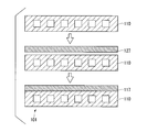
次に、本発明の第二実施形態であるヒートシンクについて説明する。図6に、本発明の第二実施形態に係るヒートシンク101を示す。
このヒートシンク101は、ヒートシンク本体110と、ヒートシンク本体110の一方の面(図6において上側)に積層された銅、ニッケル又は銀からなる金属部材層117と、を備えている。本実施形態では、金属部材層117は、図9に示すように、無酸素銅の圧延板からなる金属板127をヒートシンク本体110に接合することによって構成されている。
次に、本発明の第二実施形態であるヒートシンクについて説明する。図6に、本発明の第二実施形態に係るヒートシンク101を示す。
このヒートシンク101は、ヒートシンク本体110と、ヒートシンク本体110の一方の面(図6において上側)に積層された銅、ニッケル又は銀からなる金属部材層117と、を備えている。本実施形態では、金属部材層117は、図9に示すように、無酸素銅の圧延板からなる金属板127をヒートシンク本体110に接合することによって構成されている。
ヒートシンク本体110は、冷却媒体が流通する流路111が設けられている。このヒートシンク本体110は、Si濃度が1mass%以上25mass%以下の範囲内とされたアルミニウム合金で構成されており、具体的には、Siを9.6mass%以上12mass%以下の範囲内、Mgを0.3mass%以上15mass%以下の範囲内で含むアルミニウム合金で構成されている。上記アルミニウム合金のSi濃度は、好ましくは5mass%以上20mass%以下、より好ましくは7mass%以上13mass%以下であるが、これに限定されることはない。
ここで、ヒートシンク本体110と金属部材層117は、固相拡散接合されている。
ヒートシンク本体110と金属部材層117との接合界面には、図7に示すように、化合物層138が形成されている。この化合物層138は、ヒートシンク本体110のAl原子と、金属部材層117のCu原子とが相互拡散することによって形成される。この化合物層138においては、ヒートシンク本体110から金属部材層117に向かうにしたがい、漸次Al原子の濃度が低くなり、かつCu原子の濃度が高くなる濃度勾配を有している。
ヒートシンク本体110と金属部材層117との接合界面には、図7に示すように、化合物層138が形成されている。この化合物層138は、ヒートシンク本体110のAl原子と、金属部材層117のCu原子とが相互拡散することによって形成される。この化合物層138においては、ヒートシンク本体110から金属部材層117に向かうにしたがい、漸次Al原子の濃度が低くなり、かつCu原子の濃度が高くなる濃度勾配を有している。
この化合物層138は、CuとAlからなる金属間化合物で構成されており、本実施形態では、複数の金属間化合物が接合界面に沿って積層した構造とされている。ここで、化合物層138の厚さは、1μm以上80μm以下の範囲内、好ましくは、5μm以上80μm以下の範囲内に設定されている。
また、本実施形態では、化合物層138は、3種の金属間化合物が積層された構造とされており、ヒートシンク本体110側から金属部材層117側に向けて順に、ヒートシンク本体110と金属部材層117との接合界面に沿って、θ相、η2相が積層し、さらにζ2相、δ相、及びγ2相のうち少なくとも一つの相が積層して構成されている。
また、本実施形態では、化合物層138は、3種の金属間化合物が積層された構造とされており、ヒートシンク本体110側から金属部材層117側に向けて順に、ヒートシンク本体110と金属部材層117との接合界面に沿って、θ相、η2相が積層し、さらにζ2相、δ相、及びγ2相のうち少なくとも一つの相が積層して構成されている。
さらに、この化合物層138と金属部材層117との接合界面には、酸化物が接合界面に沿って層状に分散している。なお、本実施形態においては、この酸化物は、アルミナ(Al2O3)等のアルミニウム酸化物とされている。なお、酸化物は、化合物層138と金属部材層117との界面に分断された状態で分散しており、化合物層138と金属部材層117とが直接接触している領域も存在している。また、酸化物が、θ相、η2相もしくは、ζ2相、δ相、及びγ2相のうち少なくとも一つの相の内部に層状に分散している場合もある。
そして、この化合物層138の内部には、図7に示すように、Mgの濃度が3mass%以上とされたMg濃化層140が形成されており、このMg濃化層140の厚さが1μm以上30μm以下の範囲内とされている。Mg濃化層140のMgの濃度は、好ましくは5mass%以上15mass%以下、より好ましくは7mass%以上9mass%以下であるが、これに限定されることはない。Mg濃化層140の厚さは、好ましくは3μm以上25μm以下、より好ましくは5μm以上20μm以下であるが、これに限定されることはない。
次に、本実施形態であるヒートシンク101の製造方法について、図8及び図9を参照して説明する。
(ヒートシンク本体準備工程S101)
まず、接合するヒートシンク本体110を準備する。このとき、ヒートシンク本体110のうち金属部材層117と接合される接合面から深さ方向に50μmまでの領域におけるMg濃度を0.3mass%以上15mass%以下の範囲内とする。
本実施形態においては、上述のように、ヒートシンク本体110を構成するアルミニウム合金にMgを添加することにより、ヒートシンク本体110全体が、Mgを0.3mass%以上15mass%以下の範囲内で含む。ヒートシンク本体110のうち金属部材層117と接合される接合面から深さ方向に50μmまでの領域におけるMg濃度は、好ましくは2mass%以上10.8mass%以下、より好ましくは4.9mass%以上8.3mass%以下であるが、これに限定されることはない。
(ヒートシンク本体/金属部材層接合工程S102)
次に、図9に示すように、ヒートシンク本体110と金属部材層117となる金属板127とを積層し、積層方向に加圧(圧力1~35kgf/cm2(0.10~3.43MPa))した状態で真空加熱炉内に配置し加熱することにより、金属板127とヒートシンク本体110とを固相拡散接合する。なお、金属板127、ヒートシンク本体110のうち固相拡散接合されるそれぞれの接合面は、予め当該面の傷が除去されて平滑にされている。加圧の際の圧力は、より好ましくは8~20kgf/cm2(0.78~1.96MPa)であるが、これに限定されることはない。
ここで、真空加熱炉内の圧力は10-6Pa以上10-3Pa以下の範囲内に、加熱温度は400℃以上520℃以下、保持時間は0.25時間以上3時間以下の範囲内に設定されることが好ましい。真空加熱炉内の圧力は10-5Pa以上10-4Pa以下の範囲内に、加熱温度は480℃以上510℃以下、保持時間は0.5時間以上2時間以下の範囲内に設定されることがより好ましいが、これに限定されることはない。
このヒートシンク本体/金属部材層接合工程S102において、金属板127中のCu原子がヒートシンク本体110側に拡散していき、図7に示すように、化合物層138が形成され、この化合物層138の内部にMg濃化層140が形成される。
このようにして、本実施形態であるヒートシンク101が製造される。
以上のような構成とされた本実施形態に係るヒートシンク101によれば、ヒートシンク本体110の一方の面側に、無酸素銅の圧延板からなる金属板127を接合することによって金属部材層117が形成されているので、熱を金属部材層117によって面方向に広げることができ、放熱特性を大幅に向上させることができる。また、はんだ等を用いて他の部材とヒートシンク101とを良好に接合することができる。
また、ヒートシンク本体110が、Si濃度が1mass%以上25mass%以下の範囲内とされたアルミニウム合金で構成されており、具体的には、Siを9.6mass%以上12mass%以下の範囲内、Mgを0.3mass%以上15mass%以下の範囲内で含むアルミニウム合金で構成されているので、流路等を有する複雑な構造のヒートシンク本体110を構成することができる。
そして、本実施形態では、ヒートシンク本体110と金属部材層117との接合界面には、図7に示すように、化合物層138が形成され、この化合物層138の内部には、図7に示すように、Mgの濃度が3mass%以上とされたMg濃化層140が形成されており、このMg濃化層140の厚さが1μm以上30μm以下の範囲内とされているので、このMg濃化層140によって金属部材層117のCu原子の拡散移動が妨げられることになり、カーケンダルボイドの発生を抑制することができる。よって、積層方向における熱抵抗が低くなり、放熱特性に優れている。
また、Mg濃化層140の厚さが30μm以下とされているので、Cu原子の拡散が必要以上に制限されておらず、ヒートシンク本体110と金属部材層117とを確実に固相拡散接合することができる。
また、Mg濃化層140の厚さが30μm以下とされているので、Cu原子の拡散が必要以上に制限されておらず、ヒートシンク本体110と金属部材層117とを確実に固相拡散接合することができる。
また、本実施形態では、金属部材層117とヒートシンク本体110との接合界面が、第一実施形態のCu層13Bとヒートシンク31との接合界面と同様の構成とされているので、第一実施形態と同様の作用効果を奏することが可能となる。
以上、本発明の実施形態について説明したが、本発明はこれに限定されることはなく、その発明の技術的思想を逸脱しない範囲で適宜変更可能である。
例えば、上記実施の形態では、金属層(Cu層)又は金属部材層として銅からなるCu層が接合される場合について説明したが、Cu層に代えて、ニッケル又はニッケル合金からなるNi層、もしくは銀又は銀合金からなるAg層が接合されても良い。
例えば、上記実施の形態では、金属層(Cu層)又は金属部材層として銅からなるCu層が接合される場合について説明したが、Cu層に代えて、ニッケル又はニッケル合金からなるNi層、もしくは銀又は銀合金からなるAg層が接合されても良い。
Cu層に代えてNi層を形成した場合には、はんだ付け性が良好となり、他の部材との接合信頼性を向上できる。さらに、固相拡散接合によってNi層を形成する場合には、無電解めっき等でNiめっき膜を形成する際に行われるマスキング処理が不要なので、製造コストを低減できる。この場合、Ni層の厚さは1μm以上30μm以下とすることが望ましい。Ni層の厚さが1μm未満の場合には他の部材との接合信頼性を向上させる効果が無くなるおそれがあり、30μmを超える場合にはNi層が熱抵抗体となり効率的に熱を伝達できなくなるおそれがある。また、固相拡散接合によってNi層を形成する場合、Al層とNiの固相拡散接合については、接合温度を400℃以上520℃以下に設定するが、その他の条件は前述の実施形態と同様の条件で形成することができる。
Cu層に代えてAg層を形成した場合には、例えば酸化銀粒子と有機物からなる還元剤とを含む酸化銀ペーストを用いて他の部材を接合する際に、酸化銀ペーストの酸化銀が還元剤によって還元された銀と、接合するAg層とが同種の金属同士の接合となるため、接合信頼性を向上させることができる。さらには、熱伝導率の良好なAg層が形成されるので、熱を面方向に拡げて効率的に伝達することができる。この場合、Ag層の厚さは1μm以上20μm以下とすることが望ましい。Ag層の厚さが1μm未満の場合には他の部材との接合信頼性を向上させる効果が無くなるおそれがあり、20μmを超える場合には接合信頼性向上の効果が観られなくなり、コストの増加を招く。また、固相拡散接合によってAg層を形成する場合、Al層とAgの固相拡散接合については、接合温度を400℃以上520℃以下に設定するが、その他は前述の実施形態と同様の条件で形成することができる。
さらに、第一実施形態では、金属層13を、Al層13AとCu層13Bとを有するものとして説明したが、これに限定されることはなく、図10に示すように、金属層全体を銅又は銅合金で構成してもよい。この図10に示すヒートシンク付パワーモジュール用基板230においては、セラミックス基板11の他方の面(図10において下側)に銅板がDBC法あるいは活性金属ろう付け法等によって接合され、銅又は銅合金からなる金属層213が形成されている。そして、この金属層213とヒートシンク31とが、固相拡散接合されている。なお、図10に示すパワーモジュール用基板210においては、回路層212も銅又は銅合金によって構成されている。図10に示すパワーモジュール201は、ヒートシンク付パワーモジュール用基板230と、このヒートシンク付パワーモジュール用基板230の一方の面(図10において上面)にはんだ層2を介して接合された半導体素子3と、を備えている。
第一実施形態において、回路層を純度99質量%のアルミニウム板を接合することで形成したものとして説明したが、これに限定されることはなく、純度99.99質量%以上の純アルミニウムや、他のアルミニウム又はアルミニウム合金、銅又は銅合金等の他の金属で構成したものであってもよい。また、回路層をAl層とCu層の2層構造のものとしてもよい。これは、図10に示すパワーモジュール用基板210でも同様である。
第一の実施形態の金属層/ヒートシンク接合工程S05においては、金属層13(Cu層13B)とヒートシンク31とを積層し、積層方向に加圧した状態で真空加熱炉内に配置して加熱する構成とし、第二の実施形態のヒートシンク本体/金属部材層接合工程S102においては、ヒートシンク本体110と金属部材層117となる金属板127とを積層し、積層方向に加圧(圧力5~35kgf/cm2(0.49~3.43MPa))した状態で真空加熱炉内に配置して加熱する構成として、説明したが、これに限定されることはなく、図11に示すように、アルミニウム合金部材301(ヒートシンク31、ヒートシンク本体110)と金属部材302(金属層13、金属部材層117)とを固相拡散接合する際に通電加熱法を適用してもよい。
通電加熱を行う場合には、図11に示すように、アルミニウム合金部材301と金属部材302とを積層し、これらの積層体を、カーボン板311,311を介して一対の電極312、312によって積層方向に加圧するとともに、アルミニウム合金部材301及び金属部材302に対して通電を行う。すると、ジュール熱によってカーボン板311,311及びアルミニウム合金部材301と金属部材302が加熱され、アルミニウム合金部材301と金属部材302とが固相拡散接合される。
上述の通電加熱法においては、アルミニウム合金部材301及び金属部材302が直接通電加熱されることから、昇温速度を例えば30~100℃/minと比較的速くすることができ、短時間で固相拡散接合を行うことができる。これにより、接合面の酸化の影響が小さく、例えば大気雰囲気でも接合することが可能となる。また、アルミニウム合金部材301及び金属部材302の抵抗値や比熱によっては、これらアルミニウム合金部材301及び金属部材302に温度差が生じた状態で接合することも可能となり、熱膨張の差を小さくし、熱応力の低減を図ることもできる。
ここで、上述の通電加熱法においては、一対の電極312,312による加圧荷重は、30kgf/cm2以上100kgf/cm2以下(2.94MPa以上9.8MPa以下)の範囲内とすることが好ましい。上記加圧荷重は、50kgf/cm2以上80kgf/cm2以下(4.90MPa以上7.85MPa以下)とすることがより好ましいが、これに限定されることはない。
また、通電加熱法を適用する場合には、アルミニウム合金部材301及び金属部材302の表面粗さは、算術平均粗さRaで0.3μm以上0.6μm以下、または、最大高さRzで1.3μm以上2.3μm以下の範囲内とすることが好ましい。通常の固相拡散接合では、接合面の表面粗さは小さいことが好ましいが、通電加熱法の場合には、接合面の表面粗さが小さすぎると、界面接触抵抗が低下し、接合界面を局所的に加熱することが困難となるため、上述の範囲内とすることが好ましい。
また、通電加熱法を適用する場合には、アルミニウム合金部材301及び金属部材302の表面粗さは、算術平均粗さRaで0.3μm以上0.6μm以下、または、最大高さRzで1.3μm以上2.3μm以下の範囲内とすることが好ましい。通常の固相拡散接合では、接合面の表面粗さは小さいことが好ましいが、通電加熱法の場合には、接合面の表面粗さが小さすぎると、界面接触抵抗が低下し、接合界面を局所的に加熱することが困難となるため、上述の範囲内とすることが好ましい。
なお、第一の実施形態の金属層/ヒートシンク接合工程S05に上述の通電加熱法を用いることも可能であるが、その場合、セラミックス基板11が絶縁体であるため、例えば、カーボンからなる冶具等でカーボン板311,311を短絡する必要がある。接合条件は、上述したアルミニウム部材301と銅部材302の接合と同様である。
また、金属層13(Cu層13B)とヒートシンク31の表面粗さについては、上述したアルミニウム部材301及び銅部材302の場合と同様である。
また、金属層13(Cu層13B)とヒートシンク31の表面粗さについては、上述したアルミニウム部材301及び銅部材302の場合と同様である。
以下に、本発明の効果を確認すべく行った確認実験の結果について説明する。
(試験片の作製)
表1に示すアルミニウム合金板(50mm×50mm、厚さ5mm)の一方の面を表1記載のMg濃度となるまで研磨し、その面に表1に示す金属板(40mm×40mm、厚さは表1参照)を、上述の実施形態に記載した方法によって固相拡散接合した。
本発明例1-10及び比較例1-5においては、アルミニウム板と金属板とを積層方向に15kgf/cm2(1.47MPa)の荷重で押圧し、真空加熱炉で500℃、180minの条件で固相拡散接合を実施した。
本発明例11-15においては、アルミニウム合金板と金属板とを図11に示す通電加熱法によって固相拡散接合した。なお、電極に加圧荷重を15kgf/cm2(1.47MPa)とし、加熱温度(銅板温度)を510℃、加熱温度での保持時間を5minとし、昇温速度を80℃/minとした。また、接合雰囲気を大気雰囲気とした。
(Mg濃化層の厚さ)
固相拡散接合されたアルミニウム合金板と金属板との接合体の断面観察を行い、接合界面に形成されたMg濃化層の厚さを以下のように測定した。評価結果を表1に示す。
Mg濃化層の厚さは、アルミニウム合金板と金属板の接合界面のEPMA(電子線マイクロアナライザー)によるMgマッピング像から、Mg濃度が3mass%以上の領域の面積を測定し、測定視野の幅の寸法で除して厚さを求め、5視野の平均をMg濃化層の厚さとした。なお、測定は倍率:2000倍で行い、アルミニウム合金板と金属板の接触面を中心に積層方向に50μmの範囲で行った。
固相拡散接合されたアルミニウム合金板と金属板との接合体の断面観察を行い、接合界面に形成されたMg濃化層の厚さを以下のように測定した。評価結果を表1に示す。
Mg濃化層の厚さは、アルミニウム合金板と金属板の接合界面のEPMA(電子線マイクロアナライザー)によるMgマッピング像から、Mg濃度が3mass%以上の領域の面積を測定し、測定視野の幅の寸法で除して厚さを求め、5視野の平均をMg濃化層の厚さとした。なお、測定は倍率:2000倍で行い、アルミニウム合金板と金属板の接触面を中心に積層方向に50μmの範囲で行った。
(ヒートサイクル試験)
次に、このようにして製造された接合体において、ヒートサイクル試験を実施した。冷熱衝撃試験機エスペック社製TSB-51を使用し、試験片(ヒートシンク付パワーモジュール)に対して、液相(フロリナート)で、-40℃で5分、150℃で5分のヒートサイクルを4000回実施した。
そして、ヒートサイクル試験前における接合体の積層方向の熱抵抗と接合率、及び、ヒートサイクル試験後における接合体の積層方向の熱抵抗と接合率を以下のようにして評価した。
次に、このようにして製造された接合体において、ヒートサイクル試験を実施した。冷熱衝撃試験機エスペック社製TSB-51を使用し、試験片(ヒートシンク付パワーモジュール)に対して、液相(フロリナート)で、-40℃で5分、150℃で5分のヒートサイクルを4000回実施した。
そして、ヒートサイクル試験前における接合体の積層方向の熱抵抗と接合率、及び、ヒートサイクル試験後における接合体の積層方向の熱抵抗と接合率を以下のようにして評価した。
(接合率評価)
接合体のアルミニウム板と金属板との接合部の接合率について超音波探傷装置を用いて評価し、以下の式から算出した。ここで、初期接合面積とは、接合前における接合すべき面積、すなわちアルミニウム板の面積とした。超音波探傷像において剥離は白色部で示されることから、この白色部の面積を剥離面積とした。評価結果を表1に示す。
接合率(%)={(初期接合面積)-(剥離面積)}/(初期接合面積)×100
接合体のアルミニウム板と金属板との接合部の接合率について超音波探傷装置を用いて評価し、以下の式から算出した。ここで、初期接合面積とは、接合前における接合すべき面積、すなわちアルミニウム板の面積とした。超音波探傷像において剥離は白色部で示されることから、この白色部の面積を剥離面積とした。評価結果を表1に示す。
接合率(%)={(初期接合面積)-(剥離面積)}/(初期接合面積)×100
(熱抵抗の測定)
ヒータチップ(13mm×10mm×0.25mm)を金属板の表面に半田付けし、アルミニウム合金板を冷却器にろう付け接合した。次に、ヒータチップを100Wの電力で加熱し、熱電対を用いてヒータチップの温度を実測した。また、冷却器を流通する冷却媒体(エチレングリコール:水=9:1)の温度を実測した。そして、ヒータチップの温度と冷却媒体の温度差を電力で割った値を熱抵抗とした。
なお、Mg濃化層が形成されていない比較例1のヒートサイクル試験前の熱抵抗を基準として1とし、この比較例1との比率で熱抵抗を評価した。評価結果を表1に示す。
ヒータチップ(13mm×10mm×0.25mm)を金属板の表面に半田付けし、アルミニウム合金板を冷却器にろう付け接合した。次に、ヒータチップを100Wの電力で加熱し、熱電対を用いてヒータチップの温度を実測した。また、冷却器を流通する冷却媒体(エチレングリコール:水=9:1)の温度を実測した。そして、ヒータチップの温度と冷却媒体の温度差を電力で割った値を熱抵抗とした。
なお、Mg濃化層が形成されていない比較例1のヒートサイクル試験前の熱抵抗を基準として1とし、この比較例1との比率で熱抵抗を評価した。評価結果を表1に示す。

Mg濃化層を形成しなかった比較例1においては、本発明例と比べ熱抵抗が大きくなっていることが確認された。また、金属板としてニッケルを用いた比較例4と本発明例9及び14を比べると、比較例4の熱抵抗が大きくなっていることが確認された。同様に金属板として銀を用いた比較例5と本発明例10及び15を比べると比較例5の熱抵抗が大きくなっていることが確認された。これらは、カーケンダルボイドが形成されたためと推測される。
また、Mg濃化層の厚さが本発明の上限を超えた比較例2においては、接合率が低く、かつ、熱抵抗が大きくなった。Mg濃化層が厚く形成されているため、金属板の金属元素の拡散が抑制されたためと推測される。
さらに、Mg濃化層の厚さが本発明の下限よりも薄い比較例3においては、比較例1と同様に、抵抗が大きくなっていることが確認された。カーケンダルボイドの発生を十分に抑制できなかったためと推測される。
さらに、Mg濃化層の厚さが本発明の下限よりも薄い比較例3においては、比較例1と同様に、抵抗が大きくなっていることが確認された。カーケンダルボイドの発生を十分に抑制できなかったためと推測される。
これに対して、Mg濃化層の厚さが本発明の範囲内とされた本発明例においては、比較例に比べて熱抵抗が小さくなっており、接合率も十分高くなっていることが確認された。適正な厚さのMg濃化層を形成させることにより、金属板を構成する金属元素の拡散が抑制され、カーケンダルボイドの発生が抑制されたためと推測される。
また、通電加熱法を適用した本発明例11-15においては、大気中で接合してもアルミニウム合金板と金属板とが良好に接合されていた。
さらに、ヒートサイクル試験後の熱抵抗の上昇や接合率の低下がほぼ観られず、接合信頼性の高い接合体が得られることが確認された。
また、通電加熱法を適用した本発明例11-15においては、大気中で接合してもアルミニウム合金板と金属板とが良好に接合されていた。
さらに、ヒートサイクル試験後の熱抵抗の上昇や接合率の低下がほぼ観られず、接合信頼性の高い接合体が得られることが確認された。
以上の結果から、本発明によれば、Siを比較的多く含むアルミニウム合金からなるアルミニウム合金部材と、銅、ニッケル、又は銀からなる金属部材とが良好に接合され、積層方向の熱抵抗が低い接合体を得ることが可能であることが確認された。
本発明によれば、Siを比較的多く含むアルミニウム合金からなるアルミニウム合金部材と、銅、ニッケル、又は銀からなる金属部材とが良好に接合され、積層方向の熱抵抗が低い接合体、この接合体を備えたヒートシンク付パワーモジュール用基板及びヒートシンク、及び、接合体の製造方法、ヒートシンク付パワーモジュール用基板の製造方法、ヒートシンクの製造方法を提供することが可能となる。
10、210 パワーモジュール用基板
11 セラミックス基板
13,213 金属層
13B Cu層(金属部材)
31 ヒートシンク(アルミニウム合金部材)
40 Mg濃化層
101 ヒートシンク
110 ヒートシンク本体(アルミニウム合金部材)
117 金属部材層
140 Mg濃化層
11 セラミックス基板
13,213 金属層
13B Cu層(金属部材)
31 ヒートシンク(アルミニウム合金部材)
40 Mg濃化層
101 ヒートシンク
110 ヒートシンク本体(アルミニウム合金部材)
117 金属部材層
140 Mg濃化層
Claims (9)
- アルミニウム合金からなるアルミニウム合金部材と、銅、ニッケル、又は銀からなる金属部材とが接合された接合体であって、
前記アルミニウム合金部材は、Si濃度が1mass%以上25mass%以下の範囲内とされたアルミニウム合金で構成され、
前記アルミニウム合金部材と前記金属部材とが固相拡散接合されており、
前記アルミニウム合金部材と前記金属部材との接合界面に、前記アルミニウム合金部材のAlと前記金属部材の金属元素とが拡散して形成された化合物層を備え、
この化合物層の内部に、Mgの濃度が3mass%以上とされたMg濃化層が形成されており、前記Mg濃化層の厚さが1μm以上30μm以下の範囲内とされていることを特徴とする接合体。 - 絶縁層と、この絶縁層の一方の面に形成された回路層と、前記絶縁層の他方の面に形成された金属層と、この金属層の前記絶縁層とは反対側の面に配置されたヒートシンクと、を備えたヒートシンク付パワーモジュール用基板であって、
前記金属層のうち前記ヒートシンクとの接合面は、銅、ニッケル、又は銀で構成され、
前記ヒートシンクのうち前記金属層との接合面は、Si濃度が1mass%以上25mass%以下の範囲内とされたアルミニウム合金で構成され、
前記ヒートシンクと前記金属層とが固相拡散接合されており、
前記ヒートシンクと前記金属層との接合界面に、前記ヒートシンクのAlと前記金属層の接合面を構成する金属元素とが拡散して形成された化合物層を備え、
この化合物層の内部に、Mgの濃度が3mass%以上とされたMg濃化層が形成されており、前記Mg濃化層の厚さが1μm以上30μm以下の範囲内とされていることを特徴とするヒートシンク付パワーモジュール用基板。 - ヒートシンク本体と、前記ヒートシンク本体に接合された金属部材層と、を備えたヒートシンクであって、
前記金属部材層は、銅、ニッケル、又は銀からなり、
前記ヒートシンク本体は、Si濃度が1mass%以上25mass%以下の範囲内とされたアルミニウム合金で構成され、
前記ヒートシンク本体と前記金属部材層とが固相拡散接合されており、
前記ヒートシンク本体と前記金属部材層との接合界面に、前記ヒートシンク本体のAlと前記金属部材層を構成する金属元素とが拡散して形成された化合物層を備え、
この化合物層の内部に、Mgの濃度が3mass%以上とされたMg濃化層が形成されており、前記Mg濃化層の厚さが1μm以上30μm以下の範囲内とされていることを特徴とするヒートシンク。 - アルミニウム合金からなるアルミニウム合金部材と、銅、ニッケル、又は銀からなる金属部材とが接合されてなる接合体の製造方法であって、
前記アルミニウム合金部材は、Si濃度が1mass%以上25mass%以下の範囲内とされたアルミニウム合金で構成されており、
接合前の前記アルミニウム合金部材において、少なくとも前記金属部材との接合面から深さ方向に50μmまでの領域におけるMg濃度を0.3mass%以上15mass%以下の範囲内とし、
このアルミニウム合金部材と前記金属部材とを固相拡散接合することを特徴とする接合体の製造方法。 - 前記アルミニウム合金部材と前記金属部材とを積層し、積層方向に加圧しながら通電して加熱することにより、前記アルミニウム合金部材と前記金属部材とを固相拡散接合することを特徴とする請求項4に記載の接合体の製造方法。
- 絶縁層と、この絶縁層の一方の面に形成された回路層と、前記絶縁層の他方の面に形成された金属層と、この金属層の前記絶縁層とは反対側の面に配置されたヒートシンクと、を備えたヒートシンク付パワーモジュール用基板の製造方法であって、
前記金属層のうち前記ヒートシンクとの接合面は、銅、ニッケル、又は銀で構成され、
前記ヒートシンクのうち前記金属層との接合面は、Si濃度が1mass%以上25mass%以下の範囲内とされたアルミニウム合金で構成されており、
接合前の前記ヒートシンクにおいて、少なくとも前記金属層との接合面から深さ方向に50μmまでの領域におけるMg濃度を0.3mass%以上15mass%以下の範囲内とし、
このヒートシンクと前記金属層とを固相拡散接合することを特徴とするヒートシンク付パワーモジュール用基板の製造方法。 - 前記ヒートシンクと前記金属層とを積層し、積層方向に加圧しながら通電して加熱することにより、前記ヒートシンクと前記金属層とを固相拡散接合することを特徴とする請求項6に記載のヒートシンク付パワーモジュール用基板の製造方法。
- ヒートシンク本体と、前記ヒートシンク本体に接合された金属部材層と、を備えたヒートシンクの製造方法であって、
前記金属部材層は、銅、ニッケル、又は銀からなり、
前記ヒートシンク本体は、Si濃度が1mass%以上25mass%以下の範囲内とされたアルミニウム合金で構成されており、
接合前の前記ヒートシンク本体において、少なくとも前記金属部材層との接合面から深さ方向に50μmまでの領域におけるMg濃度を0.3mass%以上15mass%以下の範囲内とし、
このヒートシンク本体と前記金属部材層とを固相拡散接合することを特徴とするヒートシンクの製造方法。 - 前記ヒートシンク本体と前記金属部材層とを積層し、積層方向に加圧しながら通電して加熱することにより、前記ヒートシンク本体と前記金属部材層とを固相拡散接合することを特徴とする請求項8に記載のヒートシンクの製造方法。
Priority Applications (5)
| Application Number | Priority Date | Filing Date | Title |
|---|---|---|---|
| EP16780008.5A EP3285291B1 (en) | 2015-04-16 | 2016-04-11 | Bonded body, substrate for power module with heat sink, heat sink, method for producing bonded body, method for producing substrate for power module with heat sink, and method for producing heat sink |
| US15/566,385 US10319664B2 (en) | 2015-04-16 | 2016-04-11 | Bonded body, substrate for power module with heat sink, heat sink, method for producing bonded body, method for producing substrate for power module with heat sink, and method for producing heat sink |
| CN201680022071.9A CN107534033B (zh) | 2015-04-16 | 2016-04-11 | 接合体、自带散热器的功率模块用基板、散热器及接合体的制造方法、自带散热器的功率模块用基板的制造方法、散热器的制造方法 |
| KR1020177029055A KR102422607B1 (ko) | 2015-04-16 | 2016-04-11 | 접합체, 히트 싱크가 부착된 파워 모듈용 기판, 히트 싱크, 및 접합체의 제조 방법, 히트 싱크가 부착된 파워 모듈용 기판의 제조 방법, 히트 싱크의 제조 방법 |
| US15/786,820 US10410951B2 (en) | 2015-04-16 | 2017-10-18 | Bonded body, substrate for power module with heat sink, heat sink, method for producing bonded body, method for producing substrate for power module with heat sink, and method for producing heat sink |
Applications Claiming Priority (4)
| Application Number | Priority Date | Filing Date | Title |
|---|---|---|---|
| JP2015-084030 | 2015-04-16 | ||
| JP2015084030 | 2015-04-16 | ||
| JP2016033202A JP6696215B2 (ja) | 2015-04-16 | 2016-02-24 | 接合体、ヒートシンク付パワーモジュール用基板、ヒートシンク、及び、接合体の製造方法、ヒートシンク付パワーモジュール用基板の製造方法、ヒートシンクの製造方法 |
| JP2016-033202 | 2016-02-24 |
Related Child Applications (2)
| Application Number | Title | Priority Date | Filing Date |
|---|---|---|---|
| US15/566,385 A-371-Of-International US10319664B2 (en) | 2015-04-16 | 2016-04-11 | Bonded body, substrate for power module with heat sink, heat sink, method for producing bonded body, method for producing substrate for power module with heat sink, and method for producing heat sink |
| US15/786,820 Division US10410951B2 (en) | 2015-04-16 | 2017-10-18 | Bonded body, substrate for power module with heat sink, heat sink, method for producing bonded body, method for producing substrate for power module with heat sink, and method for producing heat sink |
Publications (1)
| Publication Number | Publication Date |
|---|---|
| WO2016167217A1 true WO2016167217A1 (ja) | 2016-10-20 |
Family
ID=57125941
Family Applications (1)
| Application Number | Title | Priority Date | Filing Date |
|---|---|---|---|
| PCT/JP2016/061686 WO2016167217A1 (ja) | 2015-04-16 | 2016-04-11 | 接合体、ヒートシンク付パワーモジュール用基板、ヒートシンク、及び、接合体の製造方法、ヒートシンク付パワーモジュール用基板の製造方法、ヒートシンクの製造方法 |
Country Status (1)
| Country | Link |
|---|---|
| WO (1) | WO2016167217A1 (ja) |
Cited By (2)
| Publication number | Priority date | Publication date | Assignee | Title |
|---|---|---|---|---|
| CN111226315A (zh) * | 2017-10-27 | 2020-06-02 | 三菱综合材料株式会社 | 接合体、自带散热器的绝缘电路基板及散热器 |
| CN112823417A (zh) * | 2018-11-08 | 2021-05-18 | 三菱综合材料株式会社 | 接合体、带散热器的绝缘电路基板及散热器 |
Citations (5)
| Publication number | Priority date | Publication date | Assignee | Title |
|---|---|---|---|---|
| JPS63220987A (ja) * | 1987-03-06 | 1988-09-14 | Natl Res Inst For Metals | アルミニウム及びアルミナセラミツクスの拡散接合法 |
| JPH04288983A (ja) * | 1991-01-21 | 1992-10-14 | Hakusan Seisakusho:Kk | アルミニウム材と銅材との圧接方法 |
| JP2010094683A (ja) * | 2008-10-14 | 2010-04-30 | Panasonic Corp | アルミニウム合金の拡散接合法 |
| JP2014060215A (ja) * | 2012-09-14 | 2014-04-03 | Mitsubishi Materials Corp | ヒートシンク付パワーモジュール用基板、ヒートシンク付パワーモジュール、及びヒートシンク付パワーモジュール用基板の製造方法 |
| JP2014099596A (ja) * | 2012-10-16 | 2014-05-29 | Mitsubishi Materials Corp | ヒートシンク付パワーモジュール用基板、ヒートシンク付パワーモジュール、及びヒートシンク付パワーモジュール用基板の製造方法 |
-
2016
- 2016-04-11 WO PCT/JP2016/061686 patent/WO2016167217A1/ja active Application Filing
Patent Citations (5)
| Publication number | Priority date | Publication date | Assignee | Title |
|---|---|---|---|---|
| JPS63220987A (ja) * | 1987-03-06 | 1988-09-14 | Natl Res Inst For Metals | アルミニウム及びアルミナセラミツクスの拡散接合法 |
| JPH04288983A (ja) * | 1991-01-21 | 1992-10-14 | Hakusan Seisakusho:Kk | アルミニウム材と銅材との圧接方法 |
| JP2010094683A (ja) * | 2008-10-14 | 2010-04-30 | Panasonic Corp | アルミニウム合金の拡散接合法 |
| JP2014060215A (ja) * | 2012-09-14 | 2014-04-03 | Mitsubishi Materials Corp | ヒートシンク付パワーモジュール用基板、ヒートシンク付パワーモジュール、及びヒートシンク付パワーモジュール用基板の製造方法 |
| JP2014099596A (ja) * | 2012-10-16 | 2014-05-29 | Mitsubishi Materials Corp | ヒートシンク付パワーモジュール用基板、ヒートシンク付パワーモジュール、及びヒートシンク付パワーモジュール用基板の製造方法 |
Non-Patent Citations (1)
| Title |
|---|
| See also references of EP3285291A4 * |
Cited By (4)
| Publication number | Priority date | Publication date | Assignee | Title |
|---|---|---|---|---|
| CN111226315A (zh) * | 2017-10-27 | 2020-06-02 | 三菱综合材料株式会社 | 接合体、自带散热器的绝缘电路基板及散热器 |
| CN111226315B (zh) * | 2017-10-27 | 2023-06-06 | 三菱综合材料株式会社 | 接合体、自带散热器的绝缘电路基板及散热器 |
| CN112823417A (zh) * | 2018-11-08 | 2021-05-18 | 三菱综合材料株式会社 | 接合体、带散热器的绝缘电路基板及散热器 |
| CN112823417B (zh) * | 2018-11-08 | 2024-01-23 | 三菱综合材料株式会社 | 接合体、带散热器的绝缘电路基板及散热器 |
Similar Documents
| Publication | Publication Date | Title |
|---|---|---|
| JP6696215B2 (ja) | 接合体、ヒートシンク付パワーモジュール用基板、ヒートシンク、及び、接合体の製造方法、ヒートシンク付パワーモジュール用基板の製造方法、ヒートシンクの製造方法 | |
| JP6696214B2 (ja) | 接合体、ヒートシンク付パワーモジュール用基板、ヒートシンク、及び、接合体の製造方法、ヒートシンク付パワーモジュール用基板の製造方法、ヒートシンクの製造方法 | |
| JP5614485B2 (ja) | ヒートシンク付パワーモジュール用基板、ヒートシンク付パワーモジュール、及びヒートシンク付パワーモジュール用基板の製造方法 | |
| JP6432466B2 (ja) | 接合体、ヒートシンク付パワーモジュール用基板、ヒートシンク、接合体の製造方法、ヒートシンク付パワーモジュール用基板の製造方法、及び、ヒートシンクの製造方法 | |
| WO2013147144A1 (ja) | パワーモジュール用基板、ヒートシンク付パワーモジュール用基板、パワーモジュール、及びパワーモジュール用基板の製造方法 | |
| KR102154882B1 (ko) | 파워 모듈 | |
| TWI661516B (zh) | 接合體,附散熱器電源模組用基板,散熱器,接合體的製造方法,附散熱器電源模組用基板的製造方法及散熱器的製造方法 | |
| KR102154369B1 (ko) | 파워 모듈 | |
| TWI626720B (zh) | 功率模組 | |
| JP2018170504A (ja) | ヒートシンク付き絶縁回路基板の製造方法 | |
| JP7081686B2 (ja) | 接合体、ヒートシンク付絶縁回路基板、及び、ヒートシンク | |
| WO2016167217A1 (ja) | 接合体、ヒートシンク付パワーモジュール用基板、ヒートシンク、及び、接合体の製造方法、ヒートシンク付パワーモジュール用基板の製造方法、ヒートシンクの製造方法 | |
| JP2014039062A (ja) | パワーモジュール用基板、ヒートシンク付パワーモジュール用基板、パワーモジュール、及びパワーモジュール用基板の製造方法 | |
| WO2016167218A1 (ja) | 接合体、ヒートシンク付パワーモジュール用基板、ヒートシンク、及び、接合体の製造方法、ヒートシンク付パワーモジュール用基板の製造方法、ヒートシンクの製造方法 | |
| TW201739726A (zh) | 接合體,電源模組用基板,電源模組,接合體的製造方法及電源模組用基板的製造方法 | |
| JP6673635B2 (ja) | 接合体の製造方法、ヒートシンク付パワーモジュール用基板の製造方法、ヒートシンクの製造方法、及び、接合体、ヒートシンク付パワーモジュール用基板、ヒートシンク | |
| JP6459427B2 (ja) | ヒートシンク付パワーモジュール用基板の製造方法、及び、接合体、ヒートシンク付パワーモジュール用基板、ヒートシンク | |
| JP2019087608A (ja) | 接合体、絶縁回路基板、ヒートシンク付絶縁回路基板、ヒートシンク、及び、接合体の製造方法、絶縁回路基板の製造方法、ヒートシンク付絶縁回路基板の製造方法、ヒートシンクの製造方法 | |
| JP6911805B2 (ja) | ヒートシンク付き絶縁回路基板の製造方法 | |
| WO2016143631A1 (ja) | 接合体の製造方法、ヒートシンク付パワーモジュール用基板の製造方法、及び、ヒートシンクの製造方法 |
Legal Events
| Date | Code | Title | Description |
|---|---|---|---|
| 121 | Ep: the epo has been informed by wipo that ep was designated in this application |
Ref document number: 16780008 Country of ref document: EP Kind code of ref document: A1 |
|
| ENP | Entry into the national phase |
Ref document number: 20177029055 Country of ref document: KR Kind code of ref document: A |
|
| WWE | Wipo information: entry into national phase |
Ref document number: 15566385 Country of ref document: US |
|
| NENP | Non-entry into the national phase |
Ref country code: DE |