WO2022259409A1 - 炭化珪素半導体装置 - Google Patents
炭化珪素半導体装置 Download PDFInfo
- Publication number
- WO2022259409A1 WO2022259409A1 PCT/JP2021/021890 JP2021021890W WO2022259409A1 WO 2022259409 A1 WO2022259409 A1 WO 2022259409A1 JP 2021021890 W JP2021021890 W JP 2021021890W WO 2022259409 A1 WO2022259409 A1 WO 2022259409A1
- Authority
- WO
- WIPO (PCT)
- Prior art keywords
- region
- well
- silicon carbide
- contact
- well region
- Prior art date
- Legal status (The legal status is an assumption and is not a legal conclusion. Google has not performed a legal analysis and makes no representation as to the accuracy of the status listed.)
- Ceased
Links
Images













Classifications
-
- H—ELECTRICITY
- H10—SEMICONDUCTOR DEVICES; ELECTRIC SOLID-STATE DEVICES NOT OTHERWISE PROVIDED FOR
- H10D—INORGANIC ELECTRIC SEMICONDUCTOR DEVICES
- H10D30/00—Field-effect transistors [FET]
- H10D30/60—Insulated-gate field-effect transistors [IGFET]
-
- H—ELECTRICITY
- H10—SEMICONDUCTOR DEVICES; ELECTRIC SOLID-STATE DEVICES NOT OTHERWISE PROVIDED FOR
- H10D—INORGANIC ELECTRIC SEMICONDUCTOR DEVICES
- H10D30/00—Field-effect transistors [FET]
- H10D30/01—Manufacture or treatment
- H10D30/021—Manufacture or treatment of FETs having insulated gates [IGFET]
- H10D30/028—Manufacture or treatment of FETs having insulated gates [IGFET] of double-diffused metal oxide semiconductor [DMOS] FETs
- H10D30/0291—Manufacture or treatment of FETs having insulated gates [IGFET] of double-diffused metal oxide semiconductor [DMOS] FETs of vertical DMOS [VDMOS] FETs
-
- H—ELECTRICITY
- H10—SEMICONDUCTOR DEVICES; ELECTRIC SOLID-STATE DEVICES NOT OTHERWISE PROVIDED FOR
- H10D—INORGANIC ELECTRIC SEMICONDUCTOR DEVICES
- H10D30/00—Field-effect transistors [FET]
- H10D30/60—Insulated-gate field-effect transistors [IGFET]
- H10D30/64—Double-diffused metal-oxide semiconductor [DMOS] FETs
- H10D30/66—Vertical DMOS [VDMOS] FETs
-
- H—ELECTRICITY
- H10—SEMICONDUCTOR DEVICES; ELECTRIC SOLID-STATE DEVICES NOT OTHERWISE PROVIDED FOR
- H10D—INORGANIC ELECTRIC SEMICONDUCTOR DEVICES
- H10D62/00—Semiconductor bodies, or regions thereof, of devices having potential barriers
- H10D62/10—Shapes, relative sizes or dispositions of the regions of the semiconductor bodies; Shapes of the semiconductor bodies
- H10D62/124—Shapes, relative sizes or dispositions of the regions of semiconductor bodies or of junctions between the regions
- H10D62/126—Top-view geometrical layouts of the regions or the junctions
- H10D62/127—Top-view geometrical layouts of the regions or the junctions of cellular field-effect devices, e.g. multicellular DMOS transistors or IGBTs
-
- H—ELECTRICITY
- H10—SEMICONDUCTOR DEVICES; ELECTRIC SOLID-STATE DEVICES NOT OTHERWISE PROVIDED FOR
- H10D—INORGANIC ELECTRIC SEMICONDUCTOR DEVICES
- H10D62/00—Semiconductor bodies, or regions thereof, of devices having potential barriers
- H10D62/80—Semiconductor bodies, or regions thereof, of devices having potential barriers characterised by the materials
- H10D62/83—Semiconductor bodies, or regions thereof, of devices having potential barriers characterised by the materials being Group IV materials, e.g. B-doped Si or undoped Ge
- H10D62/832—Semiconductor bodies, or regions thereof, of devices having potential barriers characterised by the materials being Group IV materials, e.g. B-doped Si or undoped Ge being Group IV materials comprising two or more elements, e.g. SiGe
- H10D62/8325—Silicon carbide
Definitions
- the present disclosure relates to a silicon carbide semiconductor device, and more particularly to a silicon carbide semiconductor device that suppresses switching loss.
- MOS Metal Oxide Semiconductor
- MOSFET Metal Oxide Semiconductor Field Effect Transistor
- An n-type MOSFET which is one of silicon carbide semiconductor devices using silicon carbide, which has a bandgap approximately three times as large as that of silicon (Si), as a semiconductor material, is used as a switching element in an inverter circuit to generate electric power. Power loss in the conversion circuit can be reduced.
- An n-type MOSFET typically has an n-type drift layer and a p-type well provided thereon, and when the MOSFET is switched from an on state to an off state, the drain voltage of the MOSFET is That is, the voltage of the drain electrode rises abruptly and changes from approximately 0V to several hundreds of volts. Then, a displacement current is generated through the parasitic capacitance existing between the p-type well and the n-type drift layer. A displacement current generated on the drain electrode side flows to the drain electrode, and a displacement current generated on the source electrode side flows to the source electrode via the p-type well or to the gate electrode via the gate insulating film capacitance. Also, when the MOSFET is switched from the off state to the on state, a displacement current flows through the p-type well in the direction opposite to that when the MOSFET is switched from the on state to the off state.
- Patent Document 1 in a MOSFET having a superjunction (SJ) structure, a first p-pillar region extending in a first direction, and a first p-pillar region and a first surface a first well region interposed therebetween and a second well spaced in a first direction relative to the first well region, the first well region and the second well region A MOSFET is formed on the surface side of .
- a gate insulating film and a gate electrode are provided on the first p-pillar region between the first well region and the second well region to form a region that does not function as a transistor. This suppresses voltage oscillation between the gate and source during switching operation.
- part of the displacement current generated in the first p-pillar region during switching operation passes through the first well region and the second well region formed on the first p-pillar region, and furthermore, Since the current flows to the source electrode via the contact regions formed on the first well region and the second well region, voltage fluctuations occur in the first well region and the second well region. As a result, due to the displacement current between the first well region and the second well region and the gate electrode and the substrate effect, the switching operation is inhibited and the switching loss increases.
- the present disclosure has been made to solve the above problems, and provides a silicon carbide semiconductor device that suppresses an increase in switching loss while suppressing voltage oscillation between the gate and source during switching operation. for the purpose.
- a silicon carbide semiconductor device is a silicon carbide semiconductor device in which a main current flows in a thickness direction of a silicon carbide substrate, and is provided on a first main surface of the silicon carbide substrate.
- a semiconductor layer a striped second conductivity type first well region provided in an upper layer portion of the semiconductor layer and extending in a first direction; a first impurity region of a conductivity type; at least one first well contact region of a second conductivity type provided in an upper layer portion of the first well region and in contact with the first impurity region on a side surface thereof; a first contact electrically connected to the region and the at least one first well contact region and electrically connected to a first main electrode provided above the semiconductor layer; and the first well region.
- stripe-shaped second electrodes spaced apart in a second direction orthogonal to the first direction, extending in the first direction, and having no impurity region of the first conductivity type therein.
- a second well region of a conductivity type at least one second well contact region of the second conductivity type provided in an upper layer portion of the second well region; a second contact electrically connected to the first main electrode provided above the semiconductor layer; and a second main surface of the silicon carbide substrate opposite to the first main surface.
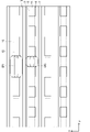
- FIG. 1 is a plan view schematically showing the configuration of a silicon carbide semiconductor device according to a first embodiment;
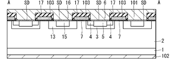
- FIG. 1 is a cross-sectional view schematically showing the configuration of a silicon carbide semiconductor device according to a first embodiment;
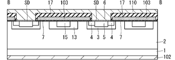
- FIG. 1 is a cross-sectional view schematically showing the configuration of a silicon carbide semiconductor device according to a first embodiment;
- FIG. 4 is a schematic diagram for explaining the effect of the silicon carbide semiconductor device of the first embodiment;
- FIG. 4 is a schematic diagram for explaining the effect of the silicon carbide semiconductor device of the first embodiment;
- FIG. 4 is a schematic diagram for explaining the effect of the silicon carbide semiconductor device of the first embodiment;
- FIG. 4 is a schematic diagram for explaining the effect of the silicon carbide semiconductor device of the first embodiment;
- FIG. 4 is a schematic diagram for explaining the effect of the silicon carbide semiconductor device of the first embodiment;
- FIG. 4 is a schematic diagram for explaining the effect of the silicon carbide semiconductor device of the first embodiment;
- FIG. 4 is a schematic diagram for explaining the effect of the silicon carbide semiconductor device of the first embodiment;
- FIG. 4 is a diagram for explaining the effect of the silicon carbide semiconductor device of the first embodiment;
- FIG. 4 is a diagram for explaining the effect of the silicon carbide semiconductor device of the first embodiment;
- FIG. 10 is a plan view schematically showing the configuration of Modification 1 of the silicon carbide semiconductor device of Embodiment 1;
- FIG. 4 is a cross-sectional view schematically showing a configuration of Modification 1 of the silicon carbide semiconductor device of Embodiment 1;
- FIG. 4 is a cross-sectional view schematically showing a configuration of Modification 1 of the silicon carbide semiconductor device of Embodiment 1;
- FIG. 4 is a cross-sectional view schematically showing a configuration of Modification 1 of the silicon carbide semiconductor device of Embodiment 1;
- FIG. 13 is a diagram schematically showing a displacement current path in the silicon carbide semiconductor device of the fifth embodiment;
- FIG. 11 is a cross-sectional view schematically showing the configuration of a silicon carbide semiconductor device according to a sixth embodiment;
- FIG. 11 is a cross-sectional view schematically showing the configuration of a silicon carbide semiconductor device according to a seventh embodiment;
- FIG. 20 is a cross-sectional view schematically showing a configuration of a modification of the silicon carbide semiconductor device of Embodiment 7;
- FIG. 20 is a cross-sectional view schematically showing the configuration of a silicon carbide semiconductor device according to an eighth embodiment;
- FIG. 21 is a cross-sectional view schematically showing the configuration of a silicon carbide semiconductor device according to a ninth embodiment;
- FIG. 20 is a cross-sectional view schematically showing the configuration of a silicon carbide semiconductor device according to a tenth embodiment;
- MOS metal-oxide-semiconductor junction structure.
- Materials for gate insulating films and gate electrodes have been improved from the viewpoint of improvement.
- polycrystalline silicon has been adopted as the material of the gate electrode instead of metal, mainly from the viewpoint of forming the source and drain in a self-aligned manner.
- a material with a high dielectric constant is employed as the material of the gate insulating film, but the material is not necessarily limited to oxide.
- MOS is not necessarily limited only to the stacked structure of metal-oxide-semiconductor, and this specification does not presuppose such a limitation. That is, in view of common technical knowledge, the term “MOS” here is not only an abbreviation derived from its etymology, but also broadly includes a layered structure of conductor-insulator-semiconductor.
- the n-type is defined as the “first conductivity type”
- the p-type which is the opposite conductivity type to the n-type
- the second conductivity type is defined as the “second conductivity type”. It is also possible to define "one conductivity type” as p-type and "second conductivity type” as n-type.
- a vertical n-type MOSFET in which the main current flows in the thickness direction of the substrate will be used as an example of the silicon carbide semiconductor device.
- a source region 4 containing a relatively high concentration of n-type (first conductivity type) impurities is formed in the well region 3, and a well containing a relatively high concentration of p-type impurities is formed in the source region 4.
- a contact region 5 (first well contact region) is formed.
- a well contact region 15 (second well contact region) containing a relatively high concentration of p-type impurities is formed in the well region 13 .
- a source contact 6 (first source contact) is provided on the source region 4 and the well contact region 5, and the source region 4 and the well contact region 5 are electrically connected to a source electrode (not shown) through the source contact 6. It is connected.
- a source contact 16 (second source contact) is provided on the well contact region 15 , and the well contact region 15 is electrically connected to a source electrode (not shown) via the source contact 16 .
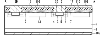
- FIG. 2 is a cross-sectional view taken along the line AA in FIG. 1 and schematically shows the configuration of the unit cell.
- n-type silicon carbide MOSFET 100 is provided on silicon carbide substrate 1 containing a relatively high concentration of n-type impurities.
- a drift layer 2 which is a semiconductor layer containing n-type impurities at a relatively low concentration is provided on the first main surface of silicon carbide substrate 1 .
- the drift layer 2 is an epitaxial growth layer formed by epitaxial growth, for example.
- a p-type well region 3 is provided in the upper layer of the drift layer 2 , and a p-type well contact region 5 is selectively provided in the upper layer of the well region 3 .
- An n-type source region 4 is provided in contact with two side surfaces of the well contact region 5 .
- the depth of the well region 3 from the outermost surface of the drift layer 2 is formed deeper than the depth of the source region 4 from the outermost surface of the drift layer 2 .
- the depth of the well contact region 5 from the outermost surface of the drift layer 2 is equal to or deeper than the depth of the source region 4 from the outermost surface of the drift layer 2, but the depth of the well region 3 It is formed so as not to exceed the depth.
- the well region 3 and the well region 13 are preferably formed separately up to the outer edge of the element, but even if they are connected to each other only at the outer edge of the element, the effect is not greatly impaired.
- a gate insulating film 7 is formed on the drift layer 2 , and a gate electrode 103 is provided on the gate insulating film 7 .
- Gate electrode 103 is provided above edges of drift layer 2 , well region 3 , well region 13 and source region 4 .
- the well contact region 5 and the source region 4 are electrically connected to the source electrode 101 through the silicide film SD and the source contact 6.
- Well contact region 15 is electrically connected to source electrode 101 via silicide film SD and source contact 16 . That is, the well regions 3 and 13 are electrically connected via the source electrode 101 .
- a drain electrode 102 is provided on the second main surface of silicon carbide substrate 1 opposite to the first main surface.
- the silicide film SD is not limited to nickel silicide, and aluminum silicide and titanium silicide can also be used.
- the source contact 6 and the source contact 16 can be formed by filling the contact hole with a metal, such as nickel, aluminum, or titanium, which is the material of the source electrode 101 when the source electrode 101 is formed.
- the impurity concentration of the n-type impurities in the drift layer 2 is preferably 1.0 ⁇ 10 14 cm ⁇ 3 or more and 1.0 ⁇ 10 17 cm ⁇ 3 or less.
- the impurity concentration of the p-type impurity in the well region 3 is preferably 1.0 ⁇ 10 16 cm ⁇ 3 or more and 1.0 ⁇ 10 20 cm ⁇ 3 or less.
- the impurity concentration of the p-type impurity in the well region 13 is preferably 1.0 ⁇ 10 16 cm ⁇ 3 or more and 1.0 ⁇ 10 20 cm ⁇ 3 or less.
- the impurity concentration of the n-type impurity in the source region 4 is preferably 1.0 ⁇ 10 17 cm ⁇ 3 or more and 1.0 ⁇ 10 21 cm ⁇ 3 or less.
- the impurity concentration of the p-type impurity in well contact region 5 is preferably 1.0 ⁇ 10 18 cm ⁇ 3 or more and 1.0 ⁇ 10 22 cm ⁇ 3 or less.
- the impurity concentration of the p-type impurity in the well contact region 15 is preferably 1.0 ⁇ 10 18 cm ⁇ 3 or more and 1.0 ⁇ 10 22 cm ⁇ 3 or less.
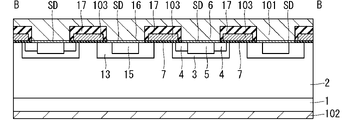
- FIG. 3 is a cross-sectional view taken along the line BB in FIG. 1 and schematically shows the configuration of the unit cell.
- the configurations of silicon carbide substrate 1, drift layer 2, well region 3, source region 4, well contact region 5, source contact 6, well region 13 and well contact region 15 are the same as in FIG.
- the gate insulating film 7 is formed on the drift layer 2 so as to straddle the edge portions of the right and left well regions 3 adjacent to the well region 13 .
- a gate electrode 103 is provided on the gate insulating film 7 .
- Gate electrode 103 is provided above edge portions of drift layer 2 , well region 3 , well region 13 , well contact region 15 and source region 4 .
- the source contact 16, which is provided so as to contact part of the well contact region 15, is not formed in the BB line cross section.
- n-type or p-type epitaxial layer with a thickness of 10 to 500 nm on the drift layer 2 and provide an epitaxial channel layer in which a channel is formed. Description and illustration are omitted in this disclosure.
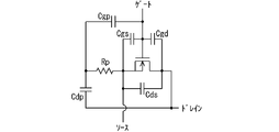
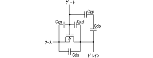
- FIG. 4 is a schematic diagram explaining the effect of the n-type silicon carbide MOSFET 100 of the first embodiment.
- Cgs is the capacitance between the gate electrode 103 and the source electrode 101 (hereinafter referred to as gate-source capacitance)
- Cgd is the capacitance between the gate electrode 103 and the drain electrode 102 (hereinafter referred to as gate-drain capacitance).
- Cds is the capacitance between the drain electrode 102 and the source electrode 101 (hereinafter referred to as drain-source capacitance)
- Cgp is the capacitance between the gate electrode 103 and the well region 13 (hereinafter referred to as gate-well capacitance)
- Cdp is the capacitance between the drain electrode 102 and the well region 13 (hereinafter referred to as drain-well capacitance).
- Rp represents the resistance component of the well region 13
- ⁇ a represents the contact resistance with respect to the well contact region 5
- ⁇ d represents the contact resistance with respect to the well contact region 15 .
- the region including the well region 13 is called a dummy region, and the other region is called a transistor region.
- FIG. 5 is an equivalent circuit diagram of the transistor area.
- the contact resistance ⁇ a is omitted for convenience.
- FIG. 6 is an equivalent circuit diagram combining the transistor area and the dummy area. Contact resistances ⁇ a and ⁇ b are omitted for convenience.
- FIG. 7 is an equivalent circuit diagram when switching the MOSFET 100 at low speed in FIG.
- the gate-to-well capacitance Cgp has been removed from FIG.
- a displacement current is generated in the well region 13 due to charging and discharging of the drain-well capacitance Cdp. flows mainly through the resistance component Rp of the well region 13 to the source electrode 101 .
- FIG. 8 is an equivalent circuit diagram when switching the MOSFET 100 at high speed in FIG.
- the resistance component Rp of the well region 13 is removed from FIG.
- a displacement current is generated in the well region 13 due to charging and discharging of the capacitance between the drain and the well.
- the displacement current mainly flows to the gate electrode 103 via Cgp. That is, in high-speed switching, the capacitive coupling between the drain electrode 102 and the gate electrode 103 effectively becomes larger than in the case of low-speed switching.
- FIG. 9 is a diagram showing simulation results of drain voltage dependence of the gate-drain capacitance Cgd in a normal MOSFET that does not have a dummy region.
- the horizontal axis indicates the drain voltage Vds (V)
- the vertical axis indicates the gate-drain capacitance Cgd (nF/cm 2 ).
- the characteristics when the switching frequencies are 10 MHz, 100 MHz and 1 GHz are indicated by a solid line, a one-dot chain line and a broken line, respectively. It can be seen from FIG. 9 that the gate-drain capacitance Cgd has a value in the vicinity of 0.1 nF/cm 2 .
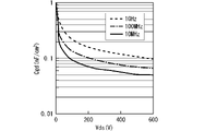
- FIG. 10 is a diagram showing a simulation result of drain voltage dependency of gate-drain capacitance Cgd in n-type silicon carbide MOSFET 100 having a dummy region.
- the horizontal axis indicates the drain voltage Vds (V)
- the vertical axis indicates the gate-drain capacitance Cgd (nF/cm 2 ).
- the characteristics when the switching frequencies are 10 MHz, 100 MHz and 1 GHz are indicated by a solid line, a one-dot chain line and a broken line, respectively.
- the values of the contact resistances ⁇ a and ⁇ b are set to be the same due to the design of the well regions 3 and 13 and the design of the well contact regions 5 and 15, respectively.
- the gate-drain capacitance Cgd at high frequencies is large, voltage fluctuations in high-frequency components can be suppressed, and voltage oscillation between the gate and source can be suppressed to reduce electromagnetic noise.
- the inter-drain capacitance Cgd is large, switching loss increases. 9 and 10, it can be seen that by using the n-type silicon carbide MOSFET 100 of the first embodiment, it is possible to reduce the switching loss while keeping the same level of electromagnetic noise. In other words, it is possible to suppress an increase in switching loss, suppress a gate-source voltage fluctuation, and reduce electromagnetic noise.
- FIG. 11 is a plan view schematically showing the configuration of n-type silicon carbide MOSFET 101 of Modification 1 of Embodiment 1.
- FIG. FIG. 12 is a cross-sectional view taken along the line AA in FIG. 11 and schematically shows the configuration of the unit cell.
- FIG. 13 is a cross-sectional view taken along the line BB in FIG. 11 and schematically shows the structure of the unit cell.
- n-type silicon carbide MOSFET 100 as shown in FIG. 2, well contact region 5 and source region 4 are in contact with source contact 6 in the same cross section, but n-type silicon carbide MOSFET 101 shown in FIGS. , the well contact region 5 is discontinuously formed in the extending direction (y-direction) of the well region 3 within the source region 4 so that the well contact region 5 and the source region 4 are aligned in the extending direction of the well region 3. , alternately, and are in contact with the source contact 6 respectively. Even when such a configuration is adopted, it is possible to suppress an increase in switching loss and reduce electromagnetic noise.
- FIG. 14 is a cross-sectional view schematically showing the configuration of n-type silicon carbide MOSFET 102 of Modification 2 of Embodiment 1, and corresponds to the cross-sectional view taken along line AA shown in FIG. 1 in the direction of the arrows. It is a diagram.
- well region 13 has only well contact region 15.
- n-type silicon carbide MOSFET 102 shown in FIG. An n-type impurity region 14 (second impurity region) having an area smaller than that of the source region 4 in a plan view is provided in the second impurity region.
- the impurity concentration of the n-type impurity in the impurity region 14 is preferably 1.0 ⁇ 10 17 cm ⁇ 3 or more and 1.0 ⁇ 10 21 cm ⁇ 3 or less like the source region 4 .
- FIG. 15 is a plan view schematically showing the configuration of n-type silicon carbide MOSFET 200 of the second embodiment according to the present disclosure.
- FIG. 16 is a cross-sectional view taken along the line BB in FIG. 15 and schematically shows the configuration of the unit cell. 15 is the same as that of FIG.
- well contact region 15 is not formed over the entire length in the extending direction of well region 13, but well contact region 15 is partially formed.
- a source contact 16 is formed only in the portion where the well contact region 15 is formed. Therefore, as shown in FIG. 16, the area below the gate electrode 103 where the well contact region 15 is not formed can be increased. Therefore, the resistance component Rp of the well region 13 can be increased, the capacitive coupling between the drain electrode 102 and the gate electrode 103 can be further increased in the high frequency region, and the effect of reducing electromagnetic noise can be enhanced. can.
- FIG. 17 is a cross-sectional view schematically showing the configuration of the n-type silicon carbide MOSFET 300 of the third embodiment according to the present disclosure, and corresponds to the cross-sectional view taken along the line AA shown in FIG. 1 in the direction of the arrows. It is a diagram.
- the impurity concentration of the well region 131 forming the dummy region is lower than the impurity concentration of the well region 3 forming the transistor region.
- the resistance component Rp of the well region 13 can be increased, the capacitive coupling between the drain electrode 102 and the gate electrode 103 can be further increased in the high frequency region, and the effect of reducing electromagnetic noise can be enhanced. can.
- the impurity concentration of the well region 131 may be made even slightly lower than the impurity concentration of the well region 3, and the effect can be obtained even by reducing it by several to 10%.
- FIG. 18 is a plan view schematically showing the configuration of n-type silicon carbide MOSFET 400 of the fourth embodiment according to the present disclosure.
- n-type silicon carbide MOSFET 400 shown in FIG. formed small.
- the width of the well region 13 may be made even slightly smaller than the width of the well region 3, and the effect can be obtained even by making it smaller by about several to 10%.
- the resistance component Rp of the well region 13 can be increased, and the capacitive coupling between the drain electrode 102 and the gate electrode 103 can be further increased in a high frequency region.
- the effect of reducing noise can be enhanced.
- FIG. 19 is a plan view schematically showing the configuration of n-type silicon carbide MOSFET 500 of the fifth embodiment according to the present disclosure.
- n-type silicon carbide MOSFET 500 shown in FIG. are alternately present in the extending direction of the well region 3 .
- the well contact regions 15 are formed discontinuously in the extending direction (y-direction) of the well regions 13, and the region interval L1 of the well contact regions 15 is set longer than the region interval L2 of the well contact regions 5. ing.
- the path length of the displacement current flowing from the well region 13 to the source electrode 101 via the well contact region 15 is equal to that of the displacement current flowing from the well region 3 to the source electrode 101 via the well contact region 5. It is formed longer than the path length.
- the path CP1 becomes longer than the path CP2, and the resistance component Rp of the well region 13 can be increased.
- Capacitive coupling between the drain electrode 102 and the gate electrode 103 in the frequency domain can be further increased, and the effect of reducing electromagnetic noise can be enhanced.
- FIG. 21 is a cross-sectional view schematically showing the configuration of n-type silicon carbide MOSFET 600 of the sixth embodiment according to the present disclosure, and corresponds to the cross-sectional view taken along line BB shown in FIG. 1 in the direction of the arrows. It is a diagram. Although the well contact region 15 is omitted in FIG. 21 for the sake of convenience, the presence or absence of the well contact region 15 does not affect the effect of this embodiment.
- the cross-sectional shape of the well region 132 has a convex shape that partially protrudes toward the drain electrode 102 side.
- the area of the pn junction interface between the well region 13 and the drift layer 2 can be increased, so that the drain-well capacitance Cdp can be increased.
- Capacitive coupling between the electrode 102 and the gate electrode 103 can be further increased, and the effect of reducing electromagnetic noise can be enhanced.
- FIG. 22 is a cross-sectional view schematically showing the configuration of n-type silicon carbide MOSFET 700 of the seventh embodiment according to the present disclosure, and corresponds to the cross-sectional view taken along line BB shown in FIG. 1 in the direction of the arrows. It is a diagram. Although the well contact region 15 is omitted in FIG. 22 for convenience, the presence or absence of the well contact region 15 does not affect the effect of this embodiment.
- an impurity region 12 (third impurity region) having a relatively high concentration of n-type impurities is provided immediately below the well region 13 .
- the impurity concentration of impurity region 12 is preferably lower than the impurity concentration of p-type impurities in well region 13 . This is to extend the depletion layer formed by the pn junction formed by the impurity region 12 and the well region 13 toward the impurity region 12 side.
- the impurity concentration of the impurity region 12 is made higher than the impurity concentration of the n-type impurity of the drift layer 2 .
- the drain-well capacitance Cdp can be increased, the capacitive coupling between the drain electrode 102 and the gate electrode 103 can be increased in a high frequency region, and the effect of reducing electromagnetic noise can be enhanced. can.
- FIG. 23 is a cross-sectional view schematically showing the configuration of n-type silicon carbide MOSFET 701 as a modification of the seventh embodiment.
- impurity region 12 extends not only directly below well region 13 but also between and directly below the impurity regions provided in the upper layer portion of drift layer 2 . is provided.
- the impurity concentration of the impurity region 12 is lower than that of the well region 3 . This is for extending the depletion layer formed by the pn junction formed by the impurity region 12 and the well region 3 toward the impurity region 12 side.
- the drain-well capacitance Cdp can be increased, the capacitive coupling between the drain electrode 102 and the gate electrode 103 can be increased in a high frequency region, and the effect of reducing electromagnetic noise can be enhanced. .
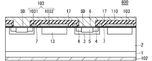
- FIG. 24 is a cross-sectional view schematically showing the configuration of an n-type silicon carbide MOSFET 800 according to the eighth embodiment of the present disclosure, and corresponds to the cross-sectional view taken along the line BB shown in FIG. 1 in the direction of the arrows. It is a diagram. Although the well contact region 15 is omitted in FIG. 24 for the sake of convenience, the presence or absence of the well contact region 15 does not affect the effects of this embodiment.
- n-type silicon carbide MOSFET 800 shown in FIG. is provided with a gate electrode 103 .
- Gate electrode 103 is provided above the edges of drift layer 2, well region 3, well region 13, well contact region 15, and source region 4.
- Gate electrode 103 provided above drift layer 2 is , has a portion 1031 (first portion) extending above well region 3 and a portion 1032 (second portion) extending above well region 13, as shown in FIG. and portion 1032 are separated.
- the ratio of the gate-well capacitance to the gate-drain capacitance Cgd can be increased, and the capacitive coupling between the drain electrode 102 and the gate electrode 103 in a high frequency region can be further increased. It is possible to enhance the effect of reducing electromagnetic noise.
- FIG. 25 is a plan view schematically showing the configuration of n-type silicon carbide MOSFET 900 of the ninth embodiment according to the present disclosure.
- the formation ratio per unit area in plan view of the well region 3 forming the transistor region and the well region 13 forming the dummy region is 1:1 as shown in FIG. Instead, it is 2:1. That is, one well region 13 is formed between two well regions 3 formed adjacent to each other and two well regions 3 formed adjacent to each other.
- the formation ratio per unit area between the well region 3 and the well region 13 is 2:1, but the formation ratio can be set arbitrarily. can be arbitrarily designed. Therefore, the switching loss reduction effect and the electromagnetic noise reduction effect can be arbitrarily set. Also, by increasing the ratio of the dummy regions, the effect of reducing electromagnetic noise can be further enhanced.
- Arbitrarily setting the formation ratio per unit area of the well region 3 and the well region 13 can be applied to any of the n-type silicon carbide MOSFETs 200 to 800 of the second to eighth embodiments.
- FIG. 26 is a plan view schematically showing the configuration of n-type silicon carbide MOSFET 1000 of the tenth embodiment according to the present disclosure.
- the source regions 4 are discontinuously formed in the extending direction (y-direction) of the well regions 3 .
- the contact resistance ⁇ d (FIG. 4) with respect to the well contact region 15 can be increased, the capacitive coupling between the drain electrode 102 and the gate electrode 103 can be further increased in the high frequency region, and electromagnetic noise can be reduced. can increase the effectiveness of
- Whether the displacement current generated in the well region 13 flows through the source electrode 101 or through the gate electrode 103 is determined by the relative magnitude relationship between the impedance of the resistance component and the capacitance component as described above. That is, increasing contact resistance ⁇ d has the same effect as increasing resistance component Rp of well region 13 in the first embodiment.
- well contact region 5 and well contact region 15 have the same p-type impurity concentration and the same contact resistivity ( ⁇ cm 2 ). can be formed to have a contact resistivity greater than that of the source contact 6 with respect to the well contact region 5 .
- the amount of overetching when opening the source contact 16 is different from the amount of overetching when opening the source contact 6 and changing the height positions of the top surfaces of the well contact region 15 and the well contact region 5, This can be achieved by making the impurity concentration of the outermost surface of well contact region 15 lower than the impurity concentration of the outermost surface of well contact region 5 . That is, when introducing impurities into the well contact regions 15 and 5, the same implantation energy and the same dose are used. The impurity concentration may be low near the surface of the impurity region.
- the impurity concentration at the top surface of the well contact region 15 is reduced to the impurity concentration at the top surface of the well contact region 5 . can be less than concentration.
- the contact resistance ⁇ d of the well contact region 15 can be increased, the capacitive coupling between the drain electrode 102 and the gate electrode 103 can be further increased in the high frequency region, and the effect of reducing electromagnetic noise can be enhanced. be able to.
- a switching element made of a silicon carbide semiconductor is suitable for high-frequency switching operation. Therefore, when applied to a converter circuit that requires a high frequency, the high switching frequency can also reduce the size of a reactor or capacitor connected to the converter circuit.
- each embodiment can be freely combined, and each embodiment can be appropriately modified or omitted.
Landscapes
- Electrodes Of Semiconductors (AREA)
Abstract
Description
図面は模式的に示されるものであり、異なる図面にそれぞれ示されている画像のサイズおよび位置の相互関係は、必ずしも正確に記載されるものではなく、適宜変更され得る。また、以下の説明では、同様の構成要素には同じ符号を付して図示し、それらの名称および機能も同様のものとする。よって、それらについての詳細な説明を省略する場合がある。また、本明細書において、「~上」および「~を覆う」という場合、構成要素間に介在物が存在することが妨げられるものではない。例えば、「A上に設けられたB」または「AがBを覆う」と記載している場合、AとBとの間に他の構成要素Cが設けられたものも設けられていないものも意味され得る。また、以下の説明では、「上」、「下」、「側」、「底」、「表」または「裏」などの特定の位置および方向を意味する用語が用いられる場合があるが、これらの用語は、実施の形態の内容を理解することを容易にするため便宜上用いられているものであり、実際に実施される際の方向とは関係しない。
本開示においては、炭化珪素半導体装置の一例として、基板の厚み方向に主電流が流れる縦型のn型炭化珪素MOSFETを主として説明する。
図11は、実施の形態1の変形例1のn型炭化珪素MOSFET101の構成を模式的に示す平面図である。また、図12は、図11におけるA-A線での矢示方向断面図であり、ユニットセルの構成を模式的に示している。また、図13は、図11におけるB-B線での矢示方向断面図であり、ユニットセルの構成を模式的に示している。
図14は、実施の形態1の変形例2のn型炭化珪素MOSFET102の構成を模式的に示す断面図であり、図1に示したA-A線での矢示方向断面図に相当する断面図である。図1および図2に示したn型炭化珪素MOSFET100では、ウェル領域13には、ウェルコンタクト領域15のみを設けた構成であったが、図14に示すn型炭化珪素MOSFET102においては、ウェル領域13にソース領域4より平面視での面積が小さなn型の不純物領域14(第2不純物領域)を設けた構成となっている。この構成を採ることで、オン抵抗を低減する効果が得られる。一方、不純物領域14を設けることによって、ウェル領域13にMOSFETが形成されたとしても、ウェル領域3のMOSFTEが存在する領域と、ウェル領域13に部分的に形成されたMOSFETが存在する領域との合計に対して、ウェル領域13のn型領域が形成されていない部分のゲート-ドレイン間容量Cgdおよびゲート-ウェル間容量Cgpがあれば、ウェル領域13にn型領域が形成されていない構成と同様に電磁ノイズを低減する効果が得られる。
図15は、本開示に係る実施の形態2のn型炭化珪素MOSFET200の構成を模式的に示す平面図である。また、図16は、図15におけるB-B線での矢示方向断面図であり、ユニットセルの構成を模式的に示している。なお、図15におけるA-A線での矢示方向断面図は図2と同じである。
図17は、本開示に係る実施の形態3のn型炭化珪素MOSFET300の構成を模式的に示す断面図であり、図1に示したA-A線での矢示方向断面図に相当する断面図である。
図18は、本開示に係る実施の形態4のn型炭化珪素MOSFET400の構成を模式的に示す平面図である。
図19は、本開示に係る実施の形態5のn型炭化珪素MOSFET500の構成を模式的に示す平面図である。
図21は、本開示に係る実施の形態6のn型炭化珪素MOSFET600の構成を模式的に示す断面図であり、図1に示したB-B線での矢示方向断面図に相当する断面図である。なお、図21では、ウェルコンタクト領域15を便宜的に省略しているが、ウェルコンタクト領域15の有無は本実施の形態の効果に影響を及ぼさない。
図22は、本開示に係る実施の形態7のn型炭化珪素MOSFET700の構成を模式的に示す断面図であり、図1に示したB-B線での矢示方向断面図に相当する断面図である。なお、図22では、ウェルコンタクト領域15を便宜的に省略しているが、ウェルコンタクト領域15の有無は本実施の形態の効果に影響を及ぼさない。
図23は、実施の形態7の変形例のn型炭化珪素MOSFET701の構成を模式的に示す断面図である。図23に示すn型炭化珪素MOSFET701においては、不純物領域12がウェル領域13の直下だけでなく、ドリフト層2の上層部に設けられた各不純物領域間および各不純物領域の直下にも及ぶように設けられている。
図24は、本開示に係る実施の形態8のn型炭化珪素MOSFET800の構成を模式的に示す断面図であり、図1に示したB-B線での矢示方向断面図に相当する断面図である。なお、図24では、ウェルコンタクト領域15を便宜的に省略しているが、ウェルコンタクト領域15の有無は本実施の形態の効果に影響を及ぼさない。
図25は、本開示に係る実施の形態9のn型炭化珪素MOSFET900の構成を模式的に示す平面図である。
図26は、本開示に係る実施の形態10のn型炭化珪素MOSFET1000の構成を模式的に示す平面図である。
実施の形態1~10においては、ウェルコンタクト領域5およびウェルコンタクト領域15のp型不純物の不純物濃度は同じとしたが、この場合、コンタクト抵抗率(Ωcm2)も同じとなるので、例えば図1に示したように、ソースコンタクト16の開口面積をソースコンタクト6の開口面積よりも小さくすることで、ウェルコンタクト領域15のコンタクト抵抗が、ウェルコンタクト領域5のコンタクト抵抗よりも大きくすることができる。
実施の形態1~10においては、ウェルコンタクト領域5およびウェルコンタクト領域15のp型不純物の不純物濃度は同じとし、コンタクト抵抗率(Ωcm2)も同じとしたが、ウェルコンタクト領域15に対するソースコンタクト16のコンタクト抵抗率を、ウェルコンタクト領域5に対するソースコンタクト6のコンタクト抵抗率よりも大きく形成することもできる。
Claims (15)
- 炭化珪素基板の厚み方向に主電流が流れる炭化珪素半導体装置であって、
前記炭化珪素基板の第1の主面上に設けられた、第1導電型の半導体層と、
前記半導体層の上層部に設けられ、第1の方向に延在するストライプ状の第2導電型の第1ウェル領域と、
前記第1ウェル領域の上層部に設けられた第1導電型の第1不純物領域と、
前記第1ウェル領域の上層部に設けられ、側面において前記第1不純物領域に接合する第2導電型の少なくとも1つの第1ウェルコンタクト領域と、
前記第1不純物領域および前記少なくとも1つの第1ウェルコンタクト領域に電気的に接続され、前記半導体層の上方に設けられた第1主電極に電気的に接続される第1コンタクトと、
前記第1ウェル領域とは、前記第1の方向とは直交する第2の方向に離間して設けられ、前記第1の方向に延在し、内部には第1導電型の不純物領域を有さないストライプ状の第2導電型の第2ウェル領域と、
前記第2ウェル領域の上層部に設けられた、第2導電型の少なくとも1つの第2ウェルコンタクト領域と、
前記少なくとも1つの第2ウェルコンタクト領域に電気的に接続され、前記半導体層の上方に設けられた前記第1主電極に電気的に接続される第2コンタクトと、
前記炭化珪素基板の前記第1の主面とは反対側の第2の主面上に設けられた第2主電極と、を備え、
前記第1ウェル領域と前記第2ウェル領域とが隣り合う領域では、
前記第1不純物領域の端縁部上、前記第1ウェル領域上、前記半導体層上、前記第2ウェル領域の端縁部上に設けられたゲート絶縁膜を介してゲート電極が設けられる、炭化珪素半導体装置。 - 炭化珪素基板の厚み方向に主電流が流れる炭化珪素半導体装置であって、
前記炭化珪素基板の第1の主面上に設けられた、第1導電型の半導体層と、
前記半導体層の上層部に設けられ、第1の方向に延在するストライプ状の第2導電型の第1ウェル領域と、
前記第1ウェル領域の上層部に設けられた第1導電型の第1不純物領域と、
前記第1ウェル領域の上層部に設けられ、側面において前記第1不純物領域に接合する第2導電型の少なくとも1つの第1ウェルコンタクト領域と、
前記第1不純物領域および前記少なくとも1つの第1ウェルコンタクト領域に電気的に接続され、前記半導体層の上方に設けられた第1主電極に電気的に接続される第1コンタクトと、
前記第1ウェル領域とは、前記第1の方向とは直交する第2の方向に離間して設けられ、前記第1の方向に延在するストライプ状の第2導電型の第2ウェル領域と、
前記第2ウェル領域の上層部に設けられた、第2導電型の少なくとも1つの第2ウェルコンタクト領域と、
前記第2ウェル領域の上層部に設けられ、前記少なくとも1つの第2ウェルコンタクト領域の側面に接合し、平面視での面積が前記第1不純物領域よりも小さい第1導電型の第2不純物領域と、
前記少なくとも1つの第2ウェルコンタクト領域に電気的に接続され、前記半導体層の上方に設けられた前記第1主電極に電気的に接続される第2コンタクトと、
前記炭化珪素基板の前記第1の主面とは反対側の第2の主面上に設けられた第2主電極と、を備え、
前記第1ウェル領域と前記第2ウェル領域とが隣り合う領域では、
前記第1不純物領域の端縁部上、前記第1ウェル領域上、前記半導体層上、前記第2ウェル領域の端縁部上に設けられたゲート絶縁膜を介してゲート電極が設けられる、炭化珪素半導体装置。 - 前記少なくとも1つの第2ウェルコンタクト領域は、
前記第2ウェル領域上において、前記第2コンタクトが設けられない部分には設けられない、請求項1または請求項2記載の炭化珪素半導体装置。 - 前記第2ウェル領域は、
前記第1ウェル領域よりも不純物濃度が小さい、請求項1または請求項2記載の炭化珪素半導体装置。 - 前記第2ウェル領域の前記第2の方向の長さは、前記第1ウェル領域の前記第2の方向の長さよりも小さい、請求項1または請求項2記載の炭化珪素半導体装置。
- 前記少なくとも1つの第1ウェルコンタクト領域および前記少なくとも1つの第2ウェルコンタクト領域は、それぞれ前記第1の方向に離間して複数形成され、
隣接する第2ウェルコンタクト領域間隔は、隣接する第1ウェルコンタクト領域間隔よりも長い、請求項1または請求項2記載の炭化珪素半導体装置。 - 前記第2ウェル領域は、
断面形状が前記第2主電極の側に部分的に突出した凸形状を有する、請求項1または請求項2記載の炭化珪素半導体装置。 - 少なくとも前記第2ウェル領域の直下に設けられ、前記半導体層よりも不純物濃度が高く、前記第2ウェル領域よりも不純物濃度が低い、第1導電型の第3不純物領域をさらに備える、請求項1または請求項2記載の炭化珪素半導体装置。
- 前記ゲート電極は、
前記第1ウェル領域と前記第2ウェル領域とが隣り合い、かつ前記第2コンタクトが設けられていない領域では、前記半導体層上から前記第1ウェル領域および前記第1不純物領域の前記端縁部にかけて延在する第1部分と、前記半導体層上から前記第2ウェル領域にかけて延在する第2部分とに分離して形成される、請求項1または請求項2記載の炭化珪素半導体装置。 - 前記第1ウェル領域および前記第2ウェル領域の平面視での単位面積当たりの形成比率が異なった比率に設定される、請求項1または請求項2記載の炭化珪素半導体装置。
- 前記第1不純物領域は、
前記第1の方向において不連続に形成される、請求項1または請求項2記載の炭化珪素半導体装置。 - 前記第2コンタクトの前記少なくとも1つの第2ウェルコンタクト領域に対するコンタクト抵抗は、前記第1コンタクトの前記少なくとも1つの第1ウェルコンタクト領域に対するコンタクト抵抗よりも大きい、請求項1または請求項2記載の炭化珪素半導体装置。
- 前記少なくとも1つの第2ウェルコンタクト領域の不純物濃度は、前記少なくとも1つの第1ウェルコンタクト領域の不純物濃度よりも低い、請求項1または請求項2記載の炭化珪素半導体装置。
- 前記少なくとも1つの第1ウェルコンタクト領域の最表面の高さ位置と、前記少なくとも1つの第2ウェルコンタクト領域の最表面の高さ位置とが異なる、請求項1または請求項2記載の炭化珪素半導体装置。
- 前記少なくとも1つの第1ウェルコンタクト領域は、前記第1の方向に沿ってストライプ状に設けられ、
前記少なくとも1つの第2ウェルコンタクト領域は、局所的に設けられる、請求項1または請求項2記載の炭化珪素半導体装置。
Priority Applications (5)
| Application Number | Priority Date | Filing Date | Title |
|---|---|---|---|
| DE112021007792.9T DE112021007792T5 (de) | 2021-06-09 | 2021-06-09 | Siliciumcarbid-halbleitereinrichtung |
| US18/287,466 US20240204056A1 (en) | 2021-06-09 | 2021-06-09 | Silicon carbide semiconductor device |
| JP2023526716A JP7515719B2 (ja) | 2021-06-09 | 2021-06-09 | 炭化珪素半導体装置 |
| PCT/JP2021/021890 WO2022259409A1 (ja) | 2021-06-09 | 2021-06-09 | 炭化珪素半導体装置 |
| CN202180098960.4A CN117425965A (zh) | 2021-06-09 | 2021-06-09 | 碳化硅半导体装置 |
Applications Claiming Priority (1)
| Application Number | Priority Date | Filing Date | Title |
|---|---|---|---|
| PCT/JP2021/021890 WO2022259409A1 (ja) | 2021-06-09 | 2021-06-09 | 炭化珪素半導体装置 |
Publications (1)
| Publication Number | Publication Date |
|---|---|
| WO2022259409A1 true WO2022259409A1 (ja) | 2022-12-15 |
Family
ID=84425922
Family Applications (1)
| Application Number | Title | Priority Date | Filing Date |
|---|---|---|---|
| PCT/JP2021/021890 Ceased WO2022259409A1 (ja) | 2021-06-09 | 2021-06-09 | 炭化珪素半導体装置 |
Country Status (5)
| Country | Link |
|---|---|
| US (1) | US20240204056A1 (ja) |
| JP (1) | JP7515719B2 (ja) |
| CN (1) | CN117425965A (ja) |
| DE (1) | DE112021007792T5 (ja) |
| WO (1) | WO2022259409A1 (ja) |
Families Citing this family (1)
| Publication number | Priority date | Publication date | Assignee | Title |
|---|---|---|---|---|
| JP7682082B2 (ja) * | 2021-11-18 | 2025-05-23 | 三菱電機株式会社 | 半導体装置および電力変換装置 |
Citations (7)
| Publication number | Priority date | Publication date | Assignee | Title |
|---|---|---|---|---|
| JP2005101551A (ja) * | 2003-08-29 | 2005-04-14 | Fuji Electric Holdings Co Ltd | 半導体装置とその製造方法およびその半導体装置を用いた双方向スイッチ素子 |
| JP2015115337A (ja) * | 2013-12-09 | 2015-06-22 | 三菱電機株式会社 | 炭化珪素半導体装置とその製造方法 |
| JP2017055145A (ja) * | 2016-12-22 | 2017-03-16 | 三菱電機株式会社 | 半導体装置 |
| JP2017168561A (ja) * | 2016-03-15 | 2017-09-21 | 富士電機株式会社 | 半導体装置及びその製造方法 |
| JP2019012803A (ja) * | 2017-07-03 | 2019-01-24 | 三菱電機株式会社 | 半導体装置 |
| WO2020026401A1 (ja) * | 2018-08-02 | 2020-02-06 | 三菱電機株式会社 | ワイドバンドギャップ半導体装置、および、電力変換装置 |
| US20200176442A1 (en) * | 2017-07-05 | 2020-06-04 | Stmicroelectronics S.R.L. | Mosfet device of silicon carbide having an integrated diode and manufacturing process thereof |
Family Cites Families (4)
| Publication number | Priority date | Publication date | Assignee | Title |
|---|---|---|---|---|
| WO2014038110A1 (ja) * | 2012-09-06 | 2014-03-13 | 三菱電機株式会社 | 半導体装置 |
| JP2019071384A (ja) | 2017-10-11 | 2019-05-09 | 株式会社東芝 | 半導体装置 |
| WO2019202350A1 (ja) * | 2018-04-19 | 2019-10-24 | 日産自動車株式会社 | 半導体装置及び半導体装置の製造方法 |
| JP6989537B2 (ja) * | 2019-01-04 | 2022-01-05 | 株式会社東芝 | 半導体装置、インバータ回路、駆動装置、車両、及び、昇降機 |
-
2021
- 2021-06-09 CN CN202180098960.4A patent/CN117425965A/zh active Pending
- 2021-06-09 WO PCT/JP2021/021890 patent/WO2022259409A1/ja not_active Ceased
- 2021-06-09 DE DE112021007792.9T patent/DE112021007792T5/de active Pending
- 2021-06-09 US US18/287,466 patent/US20240204056A1/en active Pending
- 2021-06-09 JP JP2023526716A patent/JP7515719B2/ja active Active
Patent Citations (7)
| Publication number | Priority date | Publication date | Assignee | Title |
|---|---|---|---|---|
| JP2005101551A (ja) * | 2003-08-29 | 2005-04-14 | Fuji Electric Holdings Co Ltd | 半導体装置とその製造方法およびその半導体装置を用いた双方向スイッチ素子 |
| JP2015115337A (ja) * | 2013-12-09 | 2015-06-22 | 三菱電機株式会社 | 炭化珪素半導体装置とその製造方法 |
| JP2017168561A (ja) * | 2016-03-15 | 2017-09-21 | 富士電機株式会社 | 半導体装置及びその製造方法 |
| JP2017055145A (ja) * | 2016-12-22 | 2017-03-16 | 三菱電機株式会社 | 半導体装置 |
| JP2019012803A (ja) * | 2017-07-03 | 2019-01-24 | 三菱電機株式会社 | 半導体装置 |
| US20200176442A1 (en) * | 2017-07-05 | 2020-06-04 | Stmicroelectronics S.R.L. | Mosfet device of silicon carbide having an integrated diode and manufacturing process thereof |
| WO2020026401A1 (ja) * | 2018-08-02 | 2020-02-06 | 三菱電機株式会社 | ワイドバンドギャップ半導体装置、および、電力変換装置 |
Also Published As
| Publication number | Publication date |
|---|---|
| JP7515719B2 (ja) | 2024-07-12 |
| JPWO2022259409A1 (ja) | 2022-12-15 |
| US20240204056A1 (en) | 2024-06-20 |
| CN117425965A (zh) | 2024-01-19 |
| DE112021007792T5 (de) | 2024-04-18 |
Similar Documents
| Publication | Publication Date | Title |
|---|---|---|
| CN113130627B (zh) | 一种集成沟道二极管的碳化硅鳍状栅mosfet | |
| JP4028333B2 (ja) | 半導体装置 | |
| US9184248B2 (en) | Vertical power MOSFET having planar channel and its method of fabrication | |
| US11888022B2 (en) | SOI lateral homogenization field high voltage power semiconductor device, manufacturing method and application thereof | |
| US10050113B2 (en) | Semiconductor device with needle-shaped field plates and a gate structure with edge and node portions | |
| US9412811B2 (en) | Semiconductor device having localized charge balance structure and method | |
| CN103928522B (zh) | 一种槽型积累层mosfet器件 | |
| CN109166923B (zh) | 一种屏蔽栅mosfet | |
| CN111799334A (zh) | 一种含有反向导电槽栅结构的超结mosfet | |
| CN116053325B (zh) | 一种高电阻场板屏蔽栅沟槽型场效应管器件及制造方法 | |
| US10411117B2 (en) | Semiconductor device | |
| CN115528090A (zh) | 一种双沟槽SiC MOSFET器件 | |
| CN116469924A (zh) | 漂移区电场优化的屏蔽栅mosfet | |
| CN101488500B (zh) | 半导体器件 | |
| CN104218088B (zh) | 基于折叠漂移区的soi耐压结构及功率器件 | |
| CN115425083A (zh) | 具有屏蔽栅沟槽结构的超级结半导体功率器件 | |
| WO2022044099A1 (ja) | 半導体装置、電力変換装置、および半導体装置の製造方法 | |
| CN103325835B (zh) | 一种具有结型场板的soi功率ldmos器件 | |
| CN107104149A (zh) | 一种功率半导体器件 | |
| WO2022259409A1 (ja) | 炭化珪素半導体装置 | |
| CN119562562B (zh) | 一种具有嵌入式结势垒肖特基二极管的SiC沟槽式器件 | |
| CN112864244B (zh) | 超结器件 | |
| CN108598167B (zh) | 一种具有多种部分埋层的绝缘层上硅ldmos晶体管 | |
| CN115458584B (zh) | SiC MOSFET器件结构 | |
| CN115050815B (zh) | 一种自保护的半导体结构及制造方法 |
Legal Events
| Date | Code | Title | Description |
|---|---|---|---|
| 121 | Ep: the epo has been informed by wipo that ep was designated in this application |
Ref document number: 21945086 Country of ref document: EP Kind code of ref document: A1 |
|
| ENP | Entry into the national phase |
Ref document number: 2023526716 Country of ref document: JP Kind code of ref document: A |
|
| WWE | Wipo information: entry into national phase |
Ref document number: 18287466 Country of ref document: US |
|
| WWE | Wipo information: entry into national phase |
Ref document number: 202180098960.4 Country of ref document: CN |
|
| WWE | Wipo information: entry into national phase |
Ref document number: 112021007792 Country of ref document: DE |
|
| 122 | Ep: pct application non-entry in european phase |
Ref document number: 21945086 Country of ref document: EP Kind code of ref document: A1 |