WO2022209609A1 - Dispositif à semi-conducteur - Google Patents
Dispositif à semi-conducteur Download PDFInfo
- Publication number
- WO2022209609A1 WO2022209609A1 PCT/JP2022/009762 JP2022009762W WO2022209609A1 WO 2022209609 A1 WO2022209609 A1 WO 2022209609A1 JP 2022009762 W JP2022009762 W JP 2022009762W WO 2022209609 A1 WO2022209609 A1 WO 2022209609A1
- Authority
- WO
- WIPO (PCT)
- Prior art keywords
- main surface
- semiconductor element
- semiconductor device
- bonding material
- sealing resin
- Prior art date
Links
- 239000004065 semiconductor Substances 0.000 title claims abstract description 230
- 239000011347 resin Substances 0.000 claims abstract description 118
- 229920005989 resin Polymers 0.000 claims abstract description 118
- 238000007789 sealing Methods 0.000 claims abstract description 110
- 239000000463 material Substances 0.000 claims abstract description 84
- 229910000679 solder Inorganic materials 0.000 claims description 51
- HBMJWWWQQXIZIP-UHFFFAOYSA-N silicon carbide Chemical compound [Si+]#[C-] HBMJWWWQQXIZIP-UHFFFAOYSA-N 0.000 claims description 30
- 229910010271 silicon carbide Inorganic materials 0.000 claims description 30
- 239000000758 substrate Substances 0.000 claims description 30
- 230000003746 surface roughness Effects 0.000 claims description 12
- PXHVJJICTQNCMI-UHFFFAOYSA-N Nickel Chemical compound [Ni] PXHVJJICTQNCMI-UHFFFAOYSA-N 0.000 claims description 11
- 239000002245 particle Substances 0.000 claims description 11
- 125000006850 spacer group Chemical group 0.000 claims description 8
- 229910052759 nickel Inorganic materials 0.000 claims description 5
- 230000002093 peripheral effect Effects 0.000 claims description 4
- 230000000694 effects Effects 0.000 description 9
- 239000010949 copper Substances 0.000 description 8
- 238000004519 manufacturing process Methods 0.000 description 7
- 230000008018 melting Effects 0.000 description 7
- 238000002844 melting Methods 0.000 description 7
- 229910052802 copper Inorganic materials 0.000 description 5
- 238000000034 method Methods 0.000 description 5
- 238000003892 spreading Methods 0.000 description 5
- 238000009736 wetting Methods 0.000 description 5
- RYGMFSIKBFXOCR-UHFFFAOYSA-N Copper Chemical compound [Cu] RYGMFSIKBFXOCR-UHFFFAOYSA-N 0.000 description 4
- 230000004048 modification Effects 0.000 description 4
- 238000012986 modification Methods 0.000 description 4
- XUIMIQQOPSSXEZ-UHFFFAOYSA-N Silicon Chemical compound [Si] XUIMIQQOPSSXEZ-UHFFFAOYSA-N 0.000 description 3
- 239000012141 concentrate Substances 0.000 description 3
- 229910052751 metal Inorganic materials 0.000 description 3
- 239000002184 metal Substances 0.000 description 3
- 229910052710 silicon Inorganic materials 0.000 description 3
- 239000010703 silicon Substances 0.000 description 3
- ATJFFYVFTNAWJD-UHFFFAOYSA-N Tin Chemical compound [Sn] ATJFFYVFTNAWJD-UHFFFAOYSA-N 0.000 description 2
- 238000006243 chemical reaction Methods 0.000 description 2
- 238000007747 plating Methods 0.000 description 2
- XLYOFNOQVPJJNP-UHFFFAOYSA-N water Substances O XLYOFNOQVPJJNP-UHFFFAOYSA-N 0.000 description 2
- OKTJSMMVPCPJKN-UHFFFAOYSA-N Carbon Chemical compound [C] OKTJSMMVPCPJKN-UHFFFAOYSA-N 0.000 description 1
- 239000004593 Epoxy Substances 0.000 description 1
- 229910052782 aluminium Inorganic materials 0.000 description 1
- XAGFODPZIPBFFR-UHFFFAOYSA-N aluminium Chemical compound [Al] XAGFODPZIPBFFR-UHFFFAOYSA-N 0.000 description 1
- 229910052787 antimony Inorganic materials 0.000 description 1
- 230000004888 barrier function Effects 0.000 description 1
- 229910052799 carbon Inorganic materials 0.000 description 1
- 238000003776 cleavage reaction Methods 0.000 description 1
- 239000000470 constituent Substances 0.000 description 1
- 230000032798 delamination Effects 0.000 description 1
- 230000005669 field effect Effects 0.000 description 1
- 238000010438 heat treatment Methods 0.000 description 1
- 239000012535 impurity Substances 0.000 description 1
- 230000035515 penetration Effects 0.000 description 1
- 239000002994 raw material Substances 0.000 description 1
- 238000007788 roughening Methods 0.000 description 1
- 230000007017 scission Effects 0.000 description 1
- 229910052709 silver Inorganic materials 0.000 description 1
- 239000004332 silver Substances 0.000 description 1
- 238000007711 solidification Methods 0.000 description 1
- 230000008023 solidification Effects 0.000 description 1
- 238000010998 test method Methods 0.000 description 1
- 229920001187 thermosetting polymer Polymers 0.000 description 1
Images


Classifications
-
- H—ELECTRICITY
- H01—ELECTRIC ELEMENTS
- H01L—SEMICONDUCTOR DEVICES NOT COVERED BY CLASS H10
- H01L23/00—Details of semiconductor or other solid state devices
- H01L23/28—Encapsulations, e.g. encapsulating layers, coatings, e.g. for protection
- H01L23/29—Encapsulations, e.g. encapsulating layers, coatings, e.g. for protection characterised by the material, e.g. carbon
-
- H—ELECTRICITY
- H01—ELECTRIC ELEMENTS
- H01L—SEMICONDUCTOR DEVICES NOT COVERED BY CLASS H10
- H01L23/00—Details of semiconductor or other solid state devices
- H01L23/28—Encapsulations, e.g. encapsulating layers, coatings, e.g. for protection
- H01L23/31—Encapsulations, e.g. encapsulating layers, coatings, e.g. for protection characterised by the arrangement or shape
Definitions
- the present disclosure relates to semiconductor devices.
- Patent Documents 1 and 2 structures aimed at suppressing peeling of the sealing resin have been proposed (for example, Patent Documents 1 and 2).
- a semiconductor device includes an electrode plate having a first main surface, a bonding material provided on the first main surface, a semiconductor element provided on the bonding material, the electrode plate, and the bonding material. and a sealing resin that seals the semiconductor element, and the sealing resin is provided inside at least a part of the outer edge of the semiconductor element in a plan view from a first direction perpendicular to the first main surface. At least part of the boundary between the resin and the bonding material is located.
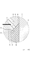
- FIG. 1 is a top view showing the semiconductor device according to the first embodiment.
- FIG. 2 is a top view showing the semiconductor device according to the first embodiment with the sealing resin and one electrode removed.
- FIG. 3 is a cross-sectional view (Part 1) showing the semiconductor device according to the first embodiment.
- FIG. 4 is a cross-sectional view (part 2) showing the semiconductor device according to the first embodiment.
- FIG. 5 is a cross-sectional view showing the stress relationship in the semiconductor device according to the first embodiment.
- FIG. 6 is a cross-sectional view showing the semiconductor device according to the second embodiment.
- FIG. 7 is a bottom view showing the semiconductor element in the semiconductor device according to the second embodiment.
- FIG. 8 is a top view showing the semiconductor device according to the third embodiment with the sealing resin and one electrode removed.
- FIG. 1 is a top view showing the semiconductor device according to the first embodiment.
- FIG. 2 is a top view showing the semiconductor device according to the first embodiment with the sealing resin and one electrode removed.
- FIG. 3 is
- FIG. 9 is a cross-sectional view (Part 1) showing the semiconductor device according to the third embodiment.
- FIG. 10 is a cross-sectional view (part 2) showing the semiconductor device according to the third embodiment.
- FIG. 11 is a cross-sectional view (Part 1) showing a semiconductor device according to a fourth embodiment.
- FIG. 12 is a cross-sectional view (Part 2) showing the semiconductor device according to the fourth embodiment.
- FIG. 13 is a bottom view showing the semiconductor element in the semiconductor device according to the fourth embodiment.
- FIG. 14 is a top view of the semiconductor device according to the fifth embodiment, excluding the sealing resin and one electrode.
- FIG. 15 is a cross-sectional view (Part 1) showing the semiconductor device according to the fifth embodiment.
- FIG. 16 is a cross-sectional view (Part 2) showing the semiconductor device according to the fifth embodiment.
- FIG. 17 is a cross-sectional view showing a semiconductor device according to the sixth embodiment.
- FIG. 18 is a cross-sectional view showing a semiconductor device according to the seventh embodiment.
- FIG. 19 is a top view showing the semiconductor device according to the eighth embodiment with the sealing resin and one electrode removed.
- FIG. 20 is a cross-sectional view (part 1) showing the semiconductor device according to the eighth embodiment.
- FIG. 21 is a cross-sectional view (Part 2) showing the semiconductor device according to the eighth embodiment.
- FIG. 22 is a top view showing the electrode plate in the semiconductor device according to the ninth embodiment.
- FIG. 23 is a cross-sectional view showing a semiconductor device according to the ninth embodiment.
- FIG. 24 is a cross-sectional view showing a modification of the silicon carbide substrate.
- a conventional semiconductor device cannot sufficiently suppress delamination. Further, in order to manufacture a conventional semiconductor device, processing such as substrate processing is required.
- An object of the present disclosure is to provide a semiconductor device that can further reduce peeling of the sealing resin.
- a semiconductor device includes an electrode plate having a first main surface, a bonding material provided on the first main surface, a semiconductor element provided on the bonding material, The electrode plate, the bonding material, and a sealing resin that seals the semiconductor element, and at least a portion of the outer edge of the semiconductor element in a plan view from a first direction perpendicular to the first main surface. At least part of the boundary between the sealing resin and the bonding material is located inside the .
- the semiconductor element when viewed in plan from the first direction, has a rectangular planar shape with a first diagonal line and a second diagonal line, and the boundary is defined by the first diagonal line Alternatively, it may be positioned inside one or both ends of the second diagonal.
- the stress in the direction of peeling off the sealing resin tends to concentrate near the corners of the semiconductor element. It is easy to suppress peeling from the vicinity of the corner.
- the boundary may be positioned inside the entire outer edge of the semiconductor element in plan view from the first direction.
- the stress in the direction opposite to the peeling direction acts on the encapsulating resin over a wide range, and the contact area between the encapsulating resin and the semiconductor element, the bonding material, or the electrode plate is large. Therefore, it is easier to suppress peeling of the sealing resin.
- the semiconductor element may have a second main surface facing the first main surface, and the sealing resin may be in contact with the second main surface. In this case, stress in the direction opposite to the peeling direction acts on the sealing resin from the second main surface, and peeling of the sealing resin can be suppressed.
- the sealing resin in plan view from the first direction, is inside at least a part of the outer edge of the semiconductor element and is in contact with the first main surface. may have parts. In this case, stress in the direction opposite to the peeling direction acts on the sealing resin from the side surface of the bonding material, and peeling of the sealing resin can be suppressed.
- the bonding material has a constricted portion positioned inside at least a part of the outer edge of the semiconductor element when viewed from above in the first direction, and when viewed in cross section,
- the constricted portion may be between the electrode plate and the semiconductor element, and the sealing resin may be in contact with the side surface of the bonding material.
- stress in the direction opposite to the peeling direction acts on the sealing resin at the constricted portion, and peeling of the sealing resin can be suppressed.
- the semiconductor element has a second main surface facing the first main surface, and an electrode having a third main surface forming part of the second main surface. , wherein the electrode is provided inside at least a part of the outer edge of the semiconductor element when viewed in plan from the first direction, and the bonding material is in contact with the third main surface. good. In this case, it is easy to control the shape of the bonding material.
- the semiconductor element has a semiconductor substrate having a fourth main surface, the electrode is provided on the fourth main surface, and is provided on at least the outer peripheral portion of the fourth main surface. A part may be exposed from the electrode. In this case, the portion of the fourth main surface exposed from the electrode is in contact with the sealing resin, and peeling of the sealing resin can be suppressed.
- the bonding material is solder
- the first main surface includes a first region in contact with the bonding material, a second region adjacent to the first region, wherein the solder wettability of the second region is lower than the solder wettability of the first region, and the bonding material may include a portion that overlaps a boundary between the first region and the second region . In this case, it is easy to control the range of the bonding material on the first main surface.
- the second region may include a solder resist film.
- the solder resist film can suppress wetting and spreading of the melted solder.
- the second region may include a nickel film.
- the nickel film can suppress wetting and spreading of the molten solder.
- the surface roughness of the second region may be greater than the surface roughness of the first region.
- the solder wets and spreads on the first region, but does not easily wet and spread on the second region.
- the bonding material may include a spacer.
- the shape of the bonding material can be controlled by controlling the distance between the electrode plate and the semiconductor element.
- the spacer may contain conductive particles.
- the distance between the electrode plate and the semiconductor element can be controlled by the size of the conductive particles.
- the spacer may include a wire bump.
- the height of the wire bump can control the distance between the electrode plate and the semiconductor element.
- the semiconductor element may have a side surface roughness Ra of 0.15 ⁇ m or more.
- the increase in contact area between the semiconductor element and the sealing resin makes it easier to suppress peeling of the sealing resin.
- the semiconductor element has a silicon carbide substrate having a fifth main surface and a plurality of side surfaces, and the fifth main surface has the ⁇ 0001 ⁇ plane in the off direction. and at least one of the plurality of side surfaces may be a plane perpendicular to the ⁇ 0001 ⁇ plane. In this case, at least one side surface becomes a surface slanted from a surface perpendicular to the main surface. Therefore, the contact area with the sealing resin is larger than that of the side surface perpendicular to the main surface, and peeling of the sealing resin can be easily suppressed.
- the semiconductor element may be a silicon carbide semiconductor element having a thickness of 200 ⁇ m or less. Since the intrusion of water is suppressed by suppressing the peeling of the encapsulating resin, even if the thickness of the semiconductor element is 200 ⁇ m or less, failure due to the intrusion of water is suppressed and good reliability is obtained.
- a plane including the X1-X2 direction and the Y1-Y2 direction is the XY plane
- a plane including the Y1-Y2 direction and the Z1-Z2 direction is the YZ plane
- a plane including the Z1-Z2 direction and the X1-X2 direction is the ZX plane.
- the Z1 direction is defined as the upward direction
- the Z2 direction is defined as the downward direction.
- planar viewing means viewing an object from the Z1 side.
- FIG. 1 is a top view showing the semiconductor device according to the first embodiment.
- FIG. 2 is a top view showing the semiconductor device according to the first embodiment with the sealing resin and one electrode removed.
- 3 and 4 are cross-sectional views showing the semiconductor device according to the first embodiment. 3 corresponds to a cross-sectional view taken along line III-III in FIG. 1, and FIG. 4 corresponds to a cross-sectional view taken along line IV-IV in FIG.
- the semiconductor device 101 mainly has an electrode plate 10, a bonding material 20, a semiconductor element 30, and a sealing resin .
- the electrode plate 10 has a main surface 11 on the Z1 side, a main surface 12 on the Z2 side, and side surfaces 13 connected to the main surfaces 11 and 12 .
- the electrode plate 10 is, for example, a metal plate such as a copper (Cu) plate. A plating film may be formed on the copper plate.
- the thickness of the electrode plate 10 is, for example, 0.3 mm or more and 3.0 mm or less.
- Main surface 11 is an example of a first main surface.
- the semiconductor element 30 has, for example, a silicon carbide substrate 40, an electrode 50, and an electrode 60.
- the semiconductor element 30 is, for example, a MOS field effect transistor (MOSFET), an insulated gate bipolar transistor (IGBT), or a Schottky barrier diode.
- MOSFET MOS field effect transistor
- IGBT insulated gate bipolar transistor
- Schottky barrier diode MOS field effect transistor
- the thickness of the semiconductor element 30 is, for example, 100 ⁇ m or more and 200 ⁇ m or less.
- Silicon carbide substrate 40 includes an impurity containing region (not shown). Silicon carbide substrate 40 has main surface 41 on the Z1 side, main surface 42 on the Z2 side, and side surfaces 43 connected to main surfaces 41 and 42 . Electrode 60 is provided on main surface 41 and electrode 50 is provided on main surface 42 . Silicon carbide substrate 40 is an example of a semiconductor substrate. The principal surface 42 is an example of a fourth principal surface, and the principal surface 41 is an example of a fifth principal surface.
- Electrode 50 has main surface 51 on the Z1 side, main surface 52 on the Z2 side, and side surface 53 connected to main surfaces 51 and 52 , and main surface 51 of electrode 50 is main surface of silicon carbide substrate 40 . It borders on 42. For example, the outer edge of the main surface 42 and the outer edge of the main surface 51 overlap each other in plan view, and the entire main surface 42 and the entire main surface 51 are in contact with each other.
- Main surface 52 is an example of a third main surface.
- Electrode 60 has main surface 61 on the Z1 side, main surface 62 on the Z2 side, and side surface 63 connected to main surfaces 61 and 62 , and main surface 62 of electrode 60 is main surface of silicon carbide substrate 40 . It borders on 41.
- the outer edge of the principal surface 62 is inside the outer edge of the principal surface 41 in plan view, and the entire principal surface 62 is in contact with a portion of the principal surface 41 .
- the entire principal surface 61 and the portion of the principal surface 41 exposed from the principal surface 61 constitute the principal surface 31 on the Z1 side of the semiconductor element 30
- the entire principal surface 52 constitutes the principal surface 32 on the Z2 side of the semiconductor element 30 .
- the side surface 43 , the side surface 53 , and the side surface 63 constitute the side surface 33 of the semiconductor element 30 .
- Principal surface 32 is an example of a second principal surface.
- the bonding material 20 is provided between the electrode plate 10 and the semiconductor element 30 to bond the electrode plate 10 and the semiconductor element 30 together.
- a bonding material 20 is provided on the main surface 11
- a semiconductor element 30 is provided on the bonding material 20 .
- the bonding material 20 has a main surface 21 on the Z1 side, a main surface 22 on the Z2 side, and side surfaces 23 connected to the main surfaces 21 and 22 .
- Main surface 21 is in contact with main surface 32 of semiconductor element 30
- main surface 22 is in contact with main surface 11 of electrode plate 10 .
- the bonding material 20 is, for example, solder such as tin (Sn)-silver (Ag)-copper (Cu) solder or tin (Sn)-antimony (Sb) solder.
- the main surface 21 of the bonding material 20 has a rectangular planar shape with rounded corners.
- the semiconductor element 30 has a rectangular planar shape with a first diagonal line 71 and a second diagonal line 72 .
- the four sides of the principal surface 21 overlap the four sides of the principal surface 32 in plan view.
- the outer edge of the main surface 21 intersects the first diagonal line 71 at two locations and intersects the second diagonal line 72 at two locations. That is, the main surface 21 is inside at least a portion of the outer edge 34 of the semiconductor element 30 in plan view.
- the outer edge of the main surface 22 of the bonding material 20 is outside the outer edge 34 of the semiconductor element 30 in plan view.
- FIG. 4 corresponds to a cross-sectional view including the first diagonal line 71 .
- the sealing resin 70 seals the electrode plate 10 , the bonding material 20 and the semiconductor element 30 .
- the sealing resin 70 is, for example, a thermosetting resin such as epoxy.
- the sealing resin 70 is in contact with a portion of the principal surface 11 , the principal surface 12 and the side surfaces 13 of the electrode plate 10 .
- the sealing resin 70 contacts the side surface 23 of the bonding material 20 .
- the sealing resin 70 is in contact with the main surface 31 and side surfaces 33 of the semiconductor element 30 .
- the sealing resin 70 enters inside both ends of the first diagonal line 71 and inside both ends of the second diagonal line 72 in plan view. That is, the sealing resin 70 penetrates inside at least a portion of the outer edge 34 of the semiconductor element 30 in plan view.
- At least part of the boundary 90 between the sealing resin 70 and the bonding material 20 is positioned inside at least part of the outer edge 34 of the semiconductor element 30 in plan view.
- the sealing resin 70 is also in contact with part of the main surface 32 of the semiconductor element 30 .
- FIG. 5 is a cross-sectional view showing the stress relationship in the semiconductor device 101 according to the first embodiment.
- FIG. 5 shows an enlarged view of region R in FIG.
- a stress F1 directed in the Z1 direction is acting on the sealing resin 70 .
- part of the stress F1 acts on part of the main surface 32 of the semiconductor element 30.
- a stress F2 directed in the Z2 direction acts on the sealing resin 70 from the main surface 32 of the semiconductor element 30 . Therefore, according to the first embodiment, peeling of the sealing resin 70 can be suppressed.
- the sealing resin 70 does not enter between the electrode plate 10 and the semiconductor element 30, that is, the case where the entire boundary 90 is not located inside the outer edge 34 in plan view, the sealing resin The contact area between 70 and semiconductor element 30 is large. This point also makes it easy to suppress peeling of the sealing resin 70 .
- a reaction stress such as the stress F2 does not occur.
- this embodiment can suppress peeling of the sealing resin 70 in the vicinity of the semiconductor element 30, which is a heat source. Therefore, peeling of the sealing resin 70 can be suppressed more easily than peeling of the sealing resin 70 due to an increase in the contact area between the electrode plate 10 and the sealing resin 70 .
- the stress in the direction of peeling off the sealing resin 70 tends to concentrate near the corners of the semiconductor element 30 .
- the sealing resin 70 enters inside the outer edge 34 of the semiconductor element 30 near the corners of the semiconductor element 30 in plan view. That is, in the vicinity of the corners of the semiconductor element 30, at least part of the boundary 90 is located inside the outer edge 34 in plan view. Therefore, according to the present embodiment, it is easy to suppress peeling of the sealing resin 70 .
- the electrode plate 10 is first prepared, and a solder material that will become the bonding material 20 is arranged on the main surface 11 of the electrode plate 10 .
- the solder material is, for example, plate solder having a rectangular planar shape.
- the plate solder it is preferable to use one whose four sides are smaller than the four sides of the semiconductor element 30 by approximately 0.1 mm or more and 0.2 mm or less in plan view.
- the semiconductor element 30 is placed on the solder material and reflow is performed. As a result, a structure in which the semiconductor element 30 is bonded to the electrode plate 10 by the bonding material 20 is obtained. After that, this structure is sealed with a sealing resin 70 .
- the semiconductor device 101 according to the first embodiment is manufactured.
- part of the electrode plate 10 extends outside the sealing resin 70 . Further, an electrode plate (not shown) connected to the electrode 60 is provided. A part of this electrode plate is sealed with the sealing resin 70, and the other part extends outside the sealing resin 70. .
- the number of electrodes 60 is not limited.
- FIG. 6 is a cross-sectional view showing the semiconductor device according to the second embodiment.
- FIG. 7 is a bottom view showing the semiconductor element in the semiconductor device according to the second embodiment. 6, like FIG. 4, corresponds to a cross-sectional view taken along line IV-IV in FIG. 1 and includes the first diagonal line 71.
- the electrode 50 has a rectangular planar shape with rounded corners.
- the four sides of the principal surface 51 and the principal surface 52 overlap the four sides of the principal surface 32 in plan view.
- the outer edges of the principal surfaces 51 and 52 intersect the first diagonal line 71 at two locations and the second diagonal line 72 at two locations. That is, the electrode 50 is provided inside at least a portion of the outer edge 34 of the semiconductor element 30 in plan view.
- the main surface 21 of the bonding material 20 contacts the main surface 52 of the electrode 50 but does not contact the main surface 42 of the silicon carbide substrate 40 . That is, a portion of the outer peripheral portion of main surface 42 is exposed from electrode 50 .
- the same effect as the first embodiment can be obtained by the second embodiment. Further, during reflow during the manufacturing process of the semiconductor device 102 , melted solder (raw material of the bonding material 20 ) wets and spreads on the main surface 52 , but does not wet and spread easily on the main surface 42 . Therefore, in the second embodiment, it is easy to control the shape of the bonding material 20 .
- FIG. 8 is a top view showing the semiconductor device according to the third embodiment with the sealing resin and one electrode removed.
- 9 and 10 are cross-sectional views showing the semiconductor device according to the third embodiment.
- FIG. 9, like FIG. 3, corresponds to a cross-sectional view taken along line III-III in FIG. Similar to FIG. 4,
- FIG. 10 corresponds to a cross-sectional view taken along line IV-IV in FIG.
- the entire main surface 21 of the bonding material 20 is inside the outer edge 34 of the semiconductor element 30 in plan view.
- the outer edge of the main surface 22 of the bonding material 20 is outside the outer edge 34 of the semiconductor element 30 in plan view, as in the first embodiment.
- the sealing resin 70 enters the inside of the entire outer edge 34 of the semiconductor element 30 in plan view, and is in annular contact with the main surface 32 of the semiconductor element 30 .
- at least a portion of the boundary 90 between the sealing resin 70 and the bonding material 20 is positioned inside the entire outer edge 34 of the semiconductor element 30 in plan view.
- the same effect as the second embodiment can be obtained by the third embodiment. Further, if the external shape and dimensions of the semiconductor element 30 are the same, in the third embodiment, the stress in the direction opposite to the peeling direction acts on the sealing resin 70 in a wider range than in the first embodiment, The contact area between the resin 70 and the main surface 32 is large. Therefore, it is easier to suppress peeling of the sealing resin 70 .
- FIG. 11 and 12 are cross-sectional views showing the semiconductor device according to the fourth embodiment.
- FIG. 13 is a bottom view showing the semiconductor element in the semiconductor device according to the fourth embodiment.
- FIG. 11, like FIG. 3, corresponds to a cross-sectional view taken along line III--III in FIG.
- FIG. 12 corresponds to a cross-sectional view taken along line IV-IV in FIG.
- the entire electrode 50 is inside the outer edge 34 of the semiconductor element 30 in plan view.
- Main surface 21 of bonding material 20 contacts main surface 52 of electrode 50 of main surface 32 of semiconductor element 30 , but does not contact main surface 42 of silicon carbide substrate 40 . That is, the outer peripheral portion of the main surface 42 is annularly exposed from the electrode 50 .
- the same effect as the third embodiment can be obtained by the fourth embodiment. Further, similarly to the second embodiment, during reflow during the manufacturing process of the semiconductor device 104, melted solder wets and spreads on the main surface 52, but does not wet and spread easily on the main surface . Therefore, in the fourth embodiment, it is easy to control the shape of the bonding material 20 .
- FIG. 14 is a top view of the semiconductor device according to the fifth embodiment, excluding the sealing resin and one electrode.
- 15 and 16 are cross-sectional views showing the semiconductor device according to the fifth embodiment.
- FIG. 15, like FIG. 3, corresponds to a cross-sectional view taken along line III--III in FIG. Similar to FIG. 4,
- FIG. 16 corresponds to a cross-sectional view taken along line IV-IV in FIG.
- the main surface 21 of the bonding material 20 has a rectangular planar shape.
- the four sides of the principal surface 21 of the bonding material 20 overlap the four sides of the principal surface 32 of the semiconductor element 30 .
- the outer edge of the main surface 21 and the outer edge of the main surface 32 overlap each other in plan view, and the entire main surface 21 and the entire main surface 32 are in contact with each other.
- the outer edge of the main surface 22 of the bonding material 20 is outside the outer edge 34 of the semiconductor element 30 in plan view, as in the first embodiment.
- the bonding material 20 has a constricted portion (sink mark) 24 located inside the outer edge 34 of the semiconductor element 30 in plan view.
- the side surface 23 is curved inward.
- the constricted portion 24 is separated from the electrode plate 10 and the semiconductor element 30 . That is, the constricted portion 24 is between the electrode plate 10 and the semiconductor element 30 .
- the sealing resin 70 is in contact with a portion of the main surface 11 of the electrode plate 10, the main surface 12, and the side surface 13.
- the sealing resin 70 contacts the side surface 23 of the bonding material 20 .
- the sealing resin 70 is in contact with the main surface 31 and side surfaces 33 of the semiconductor element 30 .
- the sealing resin 70 enters inside the outer edge 34 of the semiconductor element 30 in plan view. In other words, at least part of the boundary 90 between the sealing resin 70 and the bonding material 20 is positioned inside at least part of the outer edge 34 of the semiconductor element 30 in plan view.
- the sealing resin 70 due to heat generated by the operation of the semiconductor device 105, stress may act on the sealing resin 70 in the direction of peeling off from the main surface 11 of the electrode plate 10.
- stress in the direction opposite to the peeling direction acts on the sealing resin 70 at the constricted portion 24 .
- the contact area between the sealing resin 70 and the semiconductor element 30 is larger than when the sealing resin 70 does not enter between the electrode plate 10 and the semiconductor element 30. . Therefore, peeling of the sealing resin 70 can be suppressed also by the fifth embodiment.
- FIG. 17 is a cross-sectional view showing a semiconductor device according to the sixth embodiment. 17, like FIG. 4, corresponds to a cross-sectional view taken along line IV-IV in FIG. 1 and includes the first diagonal line 71.
- FIG. 17 is a cross-sectional view showing a semiconductor device according to the sixth embodiment. 17, like FIG. 4, corresponds to a cross-sectional view taken along line IV-IV in FIG. 1 and includes the first diagonal line 71.
- a bonding material 20 contains conductive particles 25 .
- the conductive particles 25 are, for example, particles of a high melting point metal such as nickel (Ni) or particles of carbon (C). Conductive particles 25 are an example of a spacer.
- the conductive particles 25 prevent the semiconductor element 30 from moving toward the electrode plate 10 during reflow during the manufacturing process of the semiconductor device 106 . Therefore, while the molten solder spreads over the main surfaces 11 and 32, the solder narrows between the main surfaces 11 and 32 due to the surface tension of the solder. As a result, the constricted portion 24 is easily formed. Therefore, the shape of the constricted portion 24 can be controlled according to the size of the conductive particles 25 .
- FIG. 18 is a cross-sectional view showing a semiconductor device according to the seventh embodiment. Similar to FIG. 4, FIG. 18 corresponds to a cross-sectional view taken along line IV-IV in FIG. 1 and includes first diagonal line 71.
- FIG. 18 is a cross-sectional view showing a semiconductor device according to the seventh embodiment. Similar to FIG. 4, FIG. 18 corresponds to a cross-sectional view taken along line IV-IV in FIG. 1 and includes first diagonal line 71.
- the bonding material 20 includes wire bumps 26 .
- the material of the wire bumps 26 is metal such as aluminum (Al) or copper (Cu).
- Wire bump 26 is an example of a spacer.
- the wire bumps 26 prevent the semiconductor element 30 from moving toward the electrode plate 10 side. Therefore, while the molten solder spreads over the main surfaces 11 and 32, the solder narrows between the main surfaces 11 and 32 due to the surface tension of the solder. As a result, the constricted portion 24 is easily formed. Therefore, the shape of the constricted portion 24 can be controlled according to the height of the wire bump 26 .
- the constricted portion 24 is formed along the entire circumference of the side surface 23 in the fifth to seventh embodiments, the constricted portion 24 may be formed only on a portion of the side surface 23 . In this case, it is preferable that the constricted portion 24 is located inside both ends of the first diagonal line 71 and inside both ends of the second diagonal line 72 in plan view. This is because the stress in the direction of peeling off the sealing resin 70 tends to concentrate near the corners of the semiconductor element 30 as described above.
- FIG. 19 is a top view showing the semiconductor device according to the eighth embodiment with the sealing resin and one electrode removed.
- 20 and 21 are cross-sectional views showing the semiconductor device according to the eighth embodiment.
- FIG. 20, like FIG. 3, corresponds to a cross-sectional view taken along line III--III in FIG. 21, like FIG. 4, corresponds to a cross-sectional view taken along line IV-IV in FIG. 1 and includes the first diagonal line 71.
- FIG. 20 like FIG. 3, corresponds to a cross-sectional view taken along line III--III in FIG. 21, like FIG. 4, corresponds to a cross-sectional view taken along line IV-IV in FIG. 1 and includes the first diagonal line 71.
- FIG. 20 and 21 are cross-sectional views showing the semiconductor device according to the eighth embodiment.
- FIG. 20, like FIG. 3, corresponds to a cross-sectional view taken along line III--III in FIG. 21, like FIG. 4, corresponds to a cross-sectional view taken along line IV-IV in FIG. 1 and includes the first
- the main surface 21 of the bonding material 20 has a rectangular planar shape.
- the four sides of the principal surface 21 of the bonding material 20 overlap the four sides of the principal surface 32 of the semiconductor element 30 .
- the outer edge of the main surface 21 and the outer edge of the main surface 32 overlap each other in plan view, and the entire main surface 21 and the entire main surface 32 are in contact with each other.
- the outer edge of the main surface 22 of the bonding material 20 is inside the outer edge 34 of the semiconductor element 30 in plan view.
- the sealing resin 70 is in contact with a portion of the main surface 11 of the electrode plate 10, the main surface 12, and the side surface 13.
- the sealing resin 70 contacts the side surface 23 of the bonding material 20 .
- the sealing resin 70 is in contact with the main surface 31 and side surfaces 33 of the semiconductor element 30 .
- the sealing resin 70 enters inside the outer edge 34 of the semiconductor element 30 in plan view. In other words, at least part of the boundary 90 between the sealing resin 70 and the bonding material 20 is positioned inside at least part of the outer edge 34 of the semiconductor element 30 in plan view.
- the semiconductor device 108 due to heat generated by the operation of the semiconductor device 108, stress in the direction of peeling off the sealing resin 70 from the main surface 11 of the electrode plate 10 may act. In such a case, in this embodiment, stress in the direction opposite to the peeling direction acts on the sealing resin 70 from the side surface 23 of the bonding material 20 . Also, as in the first embodiment, the contact area between the sealing resin 70 and the semiconductor element 30 is larger than when the sealing resin 70 does not enter between the electrode plate 10 and the semiconductor element 30. . Therefore, peeling of the sealing resin 70 can be suppressed also by the eighth embodiment.
- FIG. 22 is a top view showing the electrode plate in the semiconductor device according to the ninth embodiment.
- FIG. 23 is a cross-sectional view showing a semiconductor device according to the ninth embodiment. 23, like FIG. 4, corresponds to a cross-sectional view taken along line IV-IV in FIG. 1 and includes the first diagonal line 71.
- FIG. 23 is a cross-sectional view showing a semiconductor device according to the ninth embodiment. 23, like FIG. 4, corresponds to a cross-sectional view taken along line IV-IV in FIG. 1 and includes the first diagonal line 71.
- the main surface 11 of the electrode plate 10 has a first region 81 in contact with the bonding material 20 and a second region 81 adjacent to the first region 81 . region 82;
- the second area 82 is, for example, an annular area.
- a first film 83 having lower solder wettability than the electrode plate 10 is provided in the second region 82 .
- the first film 83 includes, for example, a solder resist film or a nickel film.
- the electrode plate 10 is exposed from the first film 83 in the first region 81 .
- the solder wettability of the second region 82 is lower than the solder wettability of the first region 81 .
- the bonding material 20 is in contact with the first region 81 of the main surface 11 and includes a portion that overlaps the boundary between the first region 81 and the second region 82 .
- the same effect as the eighth embodiment can be obtained by the ninth embodiment.
- the second region 82 is provided, it is easy to control the shapes of the main surface 22 and the side surface 23 of the bonding material 20 .
- the first film 83 may not be provided in the second region 82 .
- the solder wettability of the second region 82 is lower than the solder wettability of the first region 81 .
- solder ball having a size of 0.76 mm before melting is placed on each of the first sample and the second sample, and heated on a hot plate to be sufficiently melted. For example, if the solder has a melting temperature of 185° C., it is sufficiently melted by heating until the actual temperature of the substrate reaches 220° C. or higher. It is then removed from the hot plate and cooled to room temperature.
- solder wetting and spreading rate S defined by the following formula (1) was calculated according to the wetting and spreading test method. and Note that the sizes of the solder balls and the sizes of the members are only examples, and other sizes may be used.
- the solder wettability may be evaluated by melting the solder on the member and then confirming the contact angle between the solder and the member after solidification.
- the method of confirming the contact angle between the solder and the member after melting and curing may be used.
- the contact angle can be measured, for example, by the ⁇ /2 method. Desired effects can be obtained when the area with good wettability is 90 degrees or less, and the area with poor wettability is 90 degrees or more. And the greater the angular difference, the more desirable the result.
- any one of the first to fourth embodiments, any one of the fifth to seventh embodiments, and any one of the eighth to ninth embodiments may be combined with two or three. In this case, peeling of the sealing resin 70 can be further suppressed.
- the semiconductor element 30 is preferably a silicon carbide semiconductor element.
- a large stress may act on the semiconductor element 30 depending on the stress acting on the sealing resin 70 .
- silicon carbide is tougher than silicon, a silicon carbide-based semiconductor element has higher strength than a silicon-based semiconductor element and is less likely to break even when a large stress acts thereon. Also, the thermal conductivity of silicon carbide is higher than that of silicon. Therefore, if the semiconductor element 30 is a silicon carbide based semiconductor device, the heat generated in the semiconductor element 30 is easily released to the outside through the bonding material 20 and the electrode plate 10 .
- Main surface 41 of silicon carbide substrate 40 is a plane in which the ⁇ 0001 ⁇ plane is inclined in the off direction by an off angle of 8° or less, and at least one of side surfaces 43 of silicon carbide substrate 40 is a plane perpendicular to the ⁇ 0001 ⁇ plane.
- FIG. 24 is a cross-sectional view showing a modification of silicon carbide substrate 40 .
- FIG. 24 shows a first embodiment to which a modification of silicon carbide substrate 40 is applied.
- FIG. 24, like FIG. 3, corresponds to a cross-sectional view taken along line III--III in FIG.
- side surface 43A When at least one side surface 43 (side surface 43A) of silicon carbide substrate 40 is a surface perpendicular to the ⁇ 0001 ⁇ plane, side surface 43A extends from a surface (vertical surface) perpendicular to main surfaces 41 and 42. It becomes an inclined surface (inclined surface). If the distance between the main surface 41 and the main surface 42 is common, the area of the inclined surface will be larger than the area of the vertical surface. For example, if the angle of inclination from the vertical plane is ⁇ , the area of the inclined plane is 1/(cos ⁇ ) times the area of the vertical plane. Therefore, the total area of the side surfaces 43 is larger than when all the side surfaces 43 are surfaces perpendicular to the main surfaces 41 and 42 . Therefore, the contact area between the encapsulating resin 70 and the side surface 43 increases, and peeling of the encapsulating resin 70 can be further suppressed.
- Such a silicon carbide substrate 40 can be formed as follows. First, a wafer having a primary surface in which the ⁇ 0001 ⁇ plane is inclined by an off angle of 8° or less in the off direction is prepared. Next, the dicing lines are damaged by laser light irradiation or the like. Next, by applying stress to the wafer, the wafer is cleaved along the dicing lines. Since the cleavage plane is perpendicular to the ⁇ 0001 ⁇ plane, silicon carbide substrate 40 having side surface 43A perpendicular to the ⁇ 0001 ⁇ plane is obtained.
- the surface roughness Ra of side surface 43 of silicon carbide substrate 40 is preferably 0.15 ⁇ m or more, more preferably 0.17 ⁇ m or more, and still more preferably 0.19 ⁇ m or more. Since the surface roughness Ra is large, the contact area between silicon carbide substrate 40 and sealing resin 70 is large, and peeling of sealing resin 70 is easily suppressed.
- the surface roughness Ra is measured according to "JIS B 0601:2013".
- the thickness of the semiconductor element 30 may be 200 ⁇ m or less, 180 ⁇ m or less, or 160 ⁇ m or less.
- chipping may occur at the corner where side surface 43 of silicon carbide substrate 40 intersects main surface 41 or main surface 42 .
- the sealing resin 70 is likely to be caught on the silicon carbide substrate 40, so that peeling is easily suppressed.
- Electrode plate 11 main surface (first main surface) 12: Main surface 13: Side surface 20: Bonding material 21: Main surface 22: Main surface 23: Side surface 24: Constricted portion 25: Conductive particle 26: Wire bump 30: Semiconductor element 31: Main surface 32: Main surface (second main surface surface) 33: Side 34: Outer edge 40: Silicon carbide substrate (semiconductor substrate) 41: Principal surface (fifth principal surface) 42: Principal surface (fourth principal surface) 43, 43A: side surface 50: electrode 51: main surface 52: main surface (third main surface) 53: Side 60: Electrode 61: Main surface 62: Main surface 63: Side 70: Sealing resin 71: First diagonal line 72: Second diagonal line 81: First region 82: Second region 83: First film 90: Boundary 101, 102, 103, 104, 105, 106, 107, 108, 109: semiconductor devices
Abstract
L'invention concerne un dispositif à semi-conducteur comprenant : une plaque d'électrode ayant une première surface principale ; un matériau de liaison disposé sur la première surface principale ; un élément semi-conducteur disposé sur le matériau de liaison ; et une résine d'étanchéité qui scelle la plaque d'électrode, le matériau de liaison et l'élément semi-conducteur. Au moins une partie de la délimitation entre la résine d'étanchéité et le matériau de liaison est située à l'intérieur d'au moins une partie de la périphérie extérieure de l'élément semi-conducteur dans une vue en plan dans une première direction perpendiculaire à la première surface principale.
Priority Applications (1)
| Application Number | Priority Date | Filing Date | Title |
|---|---|---|---|
| JP2023510739A JPWO2022209609A1 (fr) | 2021-03-31 | 2022-03-07 |
Applications Claiming Priority (2)
| Application Number | Priority Date | Filing Date | Title |
|---|---|---|---|
| JP2021-059334 | 2021-03-31 | ||
| JP2021059334 | 2021-03-31 |
Publications (1)
| Publication Number | Publication Date |
|---|---|
| WO2022209609A1 true WO2022209609A1 (fr) | 2022-10-06 |
Family
ID=83458628
Family Applications (1)
| Application Number | Title | Priority Date | Filing Date |
|---|---|---|---|
| PCT/JP2022/009762 WO2022209609A1 (fr) | 2021-03-31 | 2022-03-07 | Dispositif à semi-conducteur |
Country Status (2)
| Country | Link |
|---|---|
| JP (1) | JPWO2022209609A1 (fr) |
| WO (1) | WO2022209609A1 (fr) |
Citations (12)
| Publication number | Priority date | Publication date | Assignee | Title |
|---|---|---|---|---|
| JPH1050927A (ja) * | 1996-08-06 | 1998-02-20 | Hitachi Chem Co Ltd | マルチチップ実装法 |
| JP2003017658A (ja) * | 2001-06-28 | 2003-01-17 | Toshiba Corp | 電力用半導体装置 |
| JP2008098584A (ja) * | 2006-10-16 | 2008-04-24 | Fuji Electric Device Technology Co Ltd | 半導体装置 |
| JP2010219211A (ja) * | 2009-03-16 | 2010-09-30 | Mitsubishi Electric Corp | 電力用半導体装置 |
| WO2013099050A1 (fr) * | 2011-12-28 | 2013-07-04 | 三菱電機株式会社 | Procédé de fabrication d'un élément semi-conducteur à carbure de silicium, élément semi-conducteur à carbure de silicium, et module à semi-conducteur à carbure de silicium |
| JP2013187494A (ja) * | 2012-03-09 | 2013-09-19 | Hitachi Ltd | 半導体装置 |
| JP2013201289A (ja) * | 2012-03-26 | 2013-10-03 | Mitsubishi Electric Corp | 半導体装置 |
| DE102015200980A1 (de) * | 2015-01-22 | 2016-07-28 | Robert Bosch Gmbh | Verbindungsanordnung zwischen einem Trägerelement und einem elektronischen Schaltungsbauteil und elektronische Baugruppe |
| JP6143687B2 (ja) * | 2014-02-18 | 2017-06-07 | 三菱電機株式会社 | 半導体装置および半導体装置の製造方法 |
| WO2017217369A1 (fr) * | 2016-06-14 | 2017-12-21 | 三菱電機株式会社 | Dispositif semi-conducteur de puissance |
| WO2018173511A1 (fr) * | 2017-03-22 | 2018-09-27 | 株式会社デンソー | Dispositif à semi-conducteurs |
| WO2020012810A1 (fr) * | 2018-07-11 | 2020-01-16 | 住友電気工業株式会社 | Dispositif à semi-conducteur au carbure de silicium |
-
2022
- 2022-03-07 JP JP2023510739A patent/JPWO2022209609A1/ja active Pending
- 2022-03-07 WO PCT/JP2022/009762 patent/WO2022209609A1/fr active Application Filing
Patent Citations (12)
| Publication number | Priority date | Publication date | Assignee | Title |
|---|---|---|---|---|
| JPH1050927A (ja) * | 1996-08-06 | 1998-02-20 | Hitachi Chem Co Ltd | マルチチップ実装法 |
| JP2003017658A (ja) * | 2001-06-28 | 2003-01-17 | Toshiba Corp | 電力用半導体装置 |
| JP2008098584A (ja) * | 2006-10-16 | 2008-04-24 | Fuji Electric Device Technology Co Ltd | 半導体装置 |
| JP2010219211A (ja) * | 2009-03-16 | 2010-09-30 | Mitsubishi Electric Corp | 電力用半導体装置 |
| WO2013099050A1 (fr) * | 2011-12-28 | 2013-07-04 | 三菱電機株式会社 | Procédé de fabrication d'un élément semi-conducteur à carbure de silicium, élément semi-conducteur à carbure de silicium, et module à semi-conducteur à carbure de silicium |
| JP2013187494A (ja) * | 2012-03-09 | 2013-09-19 | Hitachi Ltd | 半導体装置 |
| JP2013201289A (ja) * | 2012-03-26 | 2013-10-03 | Mitsubishi Electric Corp | 半導体装置 |
| JP6143687B2 (ja) * | 2014-02-18 | 2017-06-07 | 三菱電機株式会社 | 半導体装置および半導体装置の製造方法 |
| DE102015200980A1 (de) * | 2015-01-22 | 2016-07-28 | Robert Bosch Gmbh | Verbindungsanordnung zwischen einem Trägerelement und einem elektronischen Schaltungsbauteil und elektronische Baugruppe |
| WO2017217369A1 (fr) * | 2016-06-14 | 2017-12-21 | 三菱電機株式会社 | Dispositif semi-conducteur de puissance |
| WO2018173511A1 (fr) * | 2017-03-22 | 2018-09-27 | 株式会社デンソー | Dispositif à semi-conducteurs |
| WO2020012810A1 (fr) * | 2018-07-11 | 2020-01-16 | 住友電気工業株式会社 | Dispositif à semi-conducteur au carbure de silicium |
Also Published As
| Publication number | Publication date |
|---|---|
| JPWO2022209609A1 (fr) | 2022-10-06 |
Similar Documents
| Publication | Publication Date | Title |
|---|---|---|
| US10879203B2 (en) | Stud bump structure for semiconductor package assemblies | |
| TWI421991B (zh) | Semiconductor device and manufacturing method thereof | |
| US11362012B2 (en) | Semiconductor device | |
| WO2011121756A1 (fr) | Dispositif semi-conducteur et procédé pour sa fabrication | |
| JP2005277059A (ja) | 半導体装置の製造方法、半導体装置、および半導体チップ | |
| TWI470707B (zh) | 佈線板及電子元件之安裝結構 | |
| TW201519392A (zh) | 半導體裝置及其製造方法 | |
| US9825006B2 (en) | Electronic component device and manufacturing method thereof | |
| US20110140256A1 (en) | Semiconductor device, substrate and semiconductor device manufacturing method | |
| TWI587415B (zh) | 半導體裝置之製造方法 | |
| TWI652774B (zh) | 電子封裝件之製法 | |
| TWI600123B (zh) | 半導體裝置及其製造方法 | |
| JP2010165923A (ja) | 半導体装置、及びその製造方法 | |
| JP2007042762A (ja) | 半導体装置およびその実装体 | |
| JP2010118522A (ja) | 半導体装置および半導体装置の製造方法 | |
| JPH1174312A (ja) | 半導体装置およびはんだバンプの形成方法 | |
| WO2022209609A1 (fr) | Dispositif à semi-conducteur | |
| JP2005044989A (ja) | 半導体パッケージ及びその製造方法 | |
| JP6423147B2 (ja) | 電力用半導体装置およびその製造方法 | |
| TW201005894A (en) | Pillar-to-pillar flip-chip assembly | |
| JP2005252074A (ja) | 半導体装置及び電子装置 | |
| JP4688443B2 (ja) | 半導体装置の製造方法 | |
| JP2013012570A (ja) | 半導体装置および半導体装置の製造方法 | |
| US20240006287A1 (en) | Semiconductor device | |
| JP5799565B2 (ja) | 半導体装置及びその製造方法 |
Legal Events
| Date | Code | Title | Description |
|---|---|---|---|
| 121 | Ep: the epo has been informed by wipo that ep was designated in this application |
Ref document number: 22779833 Country of ref document: EP Kind code of ref document: A1 |
|
| WWE | Wipo information: entry into national phase |
Ref document number: 2023510739 Country of ref document: JP |
|
| NENP | Non-entry into the national phase |
Ref country code: DE |
|
| 122 | Ep: pct application non-entry in european phase |
Ref document number: 22779833 Country of ref document: EP Kind code of ref document: A1 |