WO2022209609A1 - Semiconductor device - Google Patents
Semiconductor device Download PDFInfo
- Publication number
- WO2022209609A1 WO2022209609A1 PCT/JP2022/009762 JP2022009762W WO2022209609A1 WO 2022209609 A1 WO2022209609 A1 WO 2022209609A1 JP 2022009762 W JP2022009762 W JP 2022009762W WO 2022209609 A1 WO2022209609 A1 WO 2022209609A1
- Authority
- WO
- WIPO (PCT)
- Prior art keywords
- main surface
- semiconductor element
- semiconductor device
- bonding material
- sealing resin
- Prior art date
Links
- 239000004065 semiconductor Substances 0.000 title claims abstract description 230
- 239000011347 resin Substances 0.000 claims abstract description 118
- 229920005989 resin Polymers 0.000 claims abstract description 118
- 238000007789 sealing Methods 0.000 claims abstract description 110
- 239000000463 material Substances 0.000 claims abstract description 84
- 229910000679 solder Inorganic materials 0.000 claims description 51
- HBMJWWWQQXIZIP-UHFFFAOYSA-N silicon carbide Chemical compound [Si+]#[C-] HBMJWWWQQXIZIP-UHFFFAOYSA-N 0.000 claims description 30
- 229910010271 silicon carbide Inorganic materials 0.000 claims description 30
- 239000000758 substrate Substances 0.000 claims description 30
- 230000003746 surface roughness Effects 0.000 claims description 12
- PXHVJJICTQNCMI-UHFFFAOYSA-N Nickel Chemical compound [Ni] PXHVJJICTQNCMI-UHFFFAOYSA-N 0.000 claims description 11
- 239000002245 particle Substances 0.000 claims description 11
- 125000006850 spacer group Chemical group 0.000 claims description 8
- 229910052759 nickel Inorganic materials 0.000 claims description 5
- 230000002093 peripheral effect Effects 0.000 claims description 4
- 230000000694 effects Effects 0.000 description 9
- 239000010949 copper Substances 0.000 description 8
- 238000004519 manufacturing process Methods 0.000 description 7
- 230000008018 melting Effects 0.000 description 7
- 238000002844 melting Methods 0.000 description 7
- 229910052802 copper Inorganic materials 0.000 description 5
- 238000000034 method Methods 0.000 description 5
- 238000003892 spreading Methods 0.000 description 5
- 238000009736 wetting Methods 0.000 description 5
- RYGMFSIKBFXOCR-UHFFFAOYSA-N Copper Chemical compound [Cu] RYGMFSIKBFXOCR-UHFFFAOYSA-N 0.000 description 4
- 230000004048 modification Effects 0.000 description 4
- 238000012986 modification Methods 0.000 description 4
- XUIMIQQOPSSXEZ-UHFFFAOYSA-N Silicon Chemical compound [Si] XUIMIQQOPSSXEZ-UHFFFAOYSA-N 0.000 description 3
- 239000012141 concentrate Substances 0.000 description 3
- 229910052751 metal Inorganic materials 0.000 description 3
- 239000002184 metal Substances 0.000 description 3
- 229910052710 silicon Inorganic materials 0.000 description 3
- 239000010703 silicon Substances 0.000 description 3
- ATJFFYVFTNAWJD-UHFFFAOYSA-N Tin Chemical compound [Sn] ATJFFYVFTNAWJD-UHFFFAOYSA-N 0.000 description 2
- 238000006243 chemical reaction Methods 0.000 description 2
- 238000007747 plating Methods 0.000 description 2
- XLYOFNOQVPJJNP-UHFFFAOYSA-N water Substances O XLYOFNOQVPJJNP-UHFFFAOYSA-N 0.000 description 2
- OKTJSMMVPCPJKN-UHFFFAOYSA-N Carbon Chemical compound [C] OKTJSMMVPCPJKN-UHFFFAOYSA-N 0.000 description 1
- 239000004593 Epoxy Substances 0.000 description 1
- 229910052782 aluminium Inorganic materials 0.000 description 1
- XAGFODPZIPBFFR-UHFFFAOYSA-N aluminium Chemical compound [Al] XAGFODPZIPBFFR-UHFFFAOYSA-N 0.000 description 1
- 229910052787 antimony Inorganic materials 0.000 description 1
- 230000004888 barrier function Effects 0.000 description 1
- 229910052799 carbon Inorganic materials 0.000 description 1
- 238000003776 cleavage reaction Methods 0.000 description 1
- 239000000470 constituent Substances 0.000 description 1
- 230000032798 delamination Effects 0.000 description 1
- 230000005669 field effect Effects 0.000 description 1
- 238000010438 heat treatment Methods 0.000 description 1
- 239000012535 impurity Substances 0.000 description 1
- 230000035515 penetration Effects 0.000 description 1
- 239000002994 raw material Substances 0.000 description 1
- 238000007788 roughening Methods 0.000 description 1
- 230000007017 scission Effects 0.000 description 1
- 229910052709 silver Inorganic materials 0.000 description 1
- 239000004332 silver Substances 0.000 description 1
- 238000007711 solidification Methods 0.000 description 1
- 230000008023 solidification Effects 0.000 description 1
- 238000010998 test method Methods 0.000 description 1
- 229920001187 thermosetting polymer Polymers 0.000 description 1
Images


Classifications
-
- H—ELECTRICITY
- H01—ELECTRIC ELEMENTS
- H01L—SEMICONDUCTOR DEVICES NOT COVERED BY CLASS H10
- H01L23/00—Details of semiconductor or other solid state devices
- H01L23/28—Encapsulations, e.g. encapsulating layers, coatings, e.g. for protection
- H01L23/29—Encapsulations, e.g. encapsulating layers, coatings, e.g. for protection characterised by the material, e.g. carbon
-
- H—ELECTRICITY
- H01—ELECTRIC ELEMENTS
- H01L—SEMICONDUCTOR DEVICES NOT COVERED BY CLASS H10
- H01L23/00—Details of semiconductor or other solid state devices
- H01L23/28—Encapsulations, e.g. encapsulating layers, coatings, e.g. for protection
- H01L23/31—Encapsulations, e.g. encapsulating layers, coatings, e.g. for protection characterised by the arrangement or shape
Definitions
- the present disclosure relates to semiconductor devices.
- Patent Documents 1 and 2 structures aimed at suppressing peeling of the sealing resin have been proposed (for example, Patent Documents 1 and 2).
- a semiconductor device includes an electrode plate having a first main surface, a bonding material provided on the first main surface, a semiconductor element provided on the bonding material, the electrode plate, and the bonding material. and a sealing resin that seals the semiconductor element, and the sealing resin is provided inside at least a part of the outer edge of the semiconductor element in a plan view from a first direction perpendicular to the first main surface. At least part of the boundary between the resin and the bonding material is located.
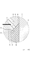
- FIG. 1 is a top view showing the semiconductor device according to the first embodiment.
- FIG. 2 is a top view showing the semiconductor device according to the first embodiment with the sealing resin and one electrode removed.
- FIG. 3 is a cross-sectional view (Part 1) showing the semiconductor device according to the first embodiment.
- FIG. 4 is a cross-sectional view (part 2) showing the semiconductor device according to the first embodiment.
- FIG. 5 is a cross-sectional view showing the stress relationship in the semiconductor device according to the first embodiment.
- FIG. 6 is a cross-sectional view showing the semiconductor device according to the second embodiment.
- FIG. 7 is a bottom view showing the semiconductor element in the semiconductor device according to the second embodiment.
- FIG. 8 is a top view showing the semiconductor device according to the third embodiment with the sealing resin and one electrode removed.
- FIG. 1 is a top view showing the semiconductor device according to the first embodiment.
- FIG. 2 is a top view showing the semiconductor device according to the first embodiment with the sealing resin and one electrode removed.
- FIG. 3 is
- FIG. 9 is a cross-sectional view (Part 1) showing the semiconductor device according to the third embodiment.
- FIG. 10 is a cross-sectional view (part 2) showing the semiconductor device according to the third embodiment.
- FIG. 11 is a cross-sectional view (Part 1) showing a semiconductor device according to a fourth embodiment.
- FIG. 12 is a cross-sectional view (Part 2) showing the semiconductor device according to the fourth embodiment.
- FIG. 13 is a bottom view showing the semiconductor element in the semiconductor device according to the fourth embodiment.
- FIG. 14 is a top view of the semiconductor device according to the fifth embodiment, excluding the sealing resin and one electrode.
- FIG. 15 is a cross-sectional view (Part 1) showing the semiconductor device according to the fifth embodiment.
- FIG. 16 is a cross-sectional view (Part 2) showing the semiconductor device according to the fifth embodiment.
- FIG. 17 is a cross-sectional view showing a semiconductor device according to the sixth embodiment.
- FIG. 18 is a cross-sectional view showing a semiconductor device according to the seventh embodiment.
- FIG. 19 is a top view showing the semiconductor device according to the eighth embodiment with the sealing resin and one electrode removed.
- FIG. 20 is a cross-sectional view (part 1) showing the semiconductor device according to the eighth embodiment.
- FIG. 21 is a cross-sectional view (Part 2) showing the semiconductor device according to the eighth embodiment.
- FIG. 22 is a top view showing the electrode plate in the semiconductor device according to the ninth embodiment.
- FIG. 23 is a cross-sectional view showing a semiconductor device according to the ninth embodiment.
- FIG. 24 is a cross-sectional view showing a modification of the silicon carbide substrate.
- a conventional semiconductor device cannot sufficiently suppress delamination. Further, in order to manufacture a conventional semiconductor device, processing such as substrate processing is required.
- An object of the present disclosure is to provide a semiconductor device that can further reduce peeling of the sealing resin.
- a semiconductor device includes an electrode plate having a first main surface, a bonding material provided on the first main surface, a semiconductor element provided on the bonding material, The electrode plate, the bonding material, and a sealing resin that seals the semiconductor element, and at least a portion of the outer edge of the semiconductor element in a plan view from a first direction perpendicular to the first main surface. At least part of the boundary between the sealing resin and the bonding material is located inside the .
- the semiconductor element when viewed in plan from the first direction, has a rectangular planar shape with a first diagonal line and a second diagonal line, and the boundary is defined by the first diagonal line Alternatively, it may be positioned inside one or both ends of the second diagonal.
- the stress in the direction of peeling off the sealing resin tends to concentrate near the corners of the semiconductor element. It is easy to suppress peeling from the vicinity of the corner.
- the boundary may be positioned inside the entire outer edge of the semiconductor element in plan view from the first direction.
- the stress in the direction opposite to the peeling direction acts on the encapsulating resin over a wide range, and the contact area between the encapsulating resin and the semiconductor element, the bonding material, or the electrode plate is large. Therefore, it is easier to suppress peeling of the sealing resin.
- the semiconductor element may have a second main surface facing the first main surface, and the sealing resin may be in contact with the second main surface. In this case, stress in the direction opposite to the peeling direction acts on the sealing resin from the second main surface, and peeling of the sealing resin can be suppressed.
- the sealing resin in plan view from the first direction, is inside at least a part of the outer edge of the semiconductor element and is in contact with the first main surface. may have parts. In this case, stress in the direction opposite to the peeling direction acts on the sealing resin from the side surface of the bonding material, and peeling of the sealing resin can be suppressed.
- the bonding material has a constricted portion positioned inside at least a part of the outer edge of the semiconductor element when viewed from above in the first direction, and when viewed in cross section,
- the constricted portion may be between the electrode plate and the semiconductor element, and the sealing resin may be in contact with the side surface of the bonding material.
- stress in the direction opposite to the peeling direction acts on the sealing resin at the constricted portion, and peeling of the sealing resin can be suppressed.
- the semiconductor element has a second main surface facing the first main surface, and an electrode having a third main surface forming part of the second main surface. , wherein the electrode is provided inside at least a part of the outer edge of the semiconductor element when viewed in plan from the first direction, and the bonding material is in contact with the third main surface. good. In this case, it is easy to control the shape of the bonding material.
- the semiconductor element has a semiconductor substrate having a fourth main surface, the electrode is provided on the fourth main surface, and is provided on at least the outer peripheral portion of the fourth main surface. A part may be exposed from the electrode. In this case, the portion of the fourth main surface exposed from the electrode is in contact with the sealing resin, and peeling of the sealing resin can be suppressed.
- the bonding material is solder
- the first main surface includes a first region in contact with the bonding material, a second region adjacent to the first region, wherein the solder wettability of the second region is lower than the solder wettability of the first region, and the bonding material may include a portion that overlaps a boundary between the first region and the second region . In this case, it is easy to control the range of the bonding material on the first main surface.
- the second region may include a solder resist film.
- the solder resist film can suppress wetting and spreading of the melted solder.
- the second region may include a nickel film.
- the nickel film can suppress wetting and spreading of the molten solder.
- the surface roughness of the second region may be greater than the surface roughness of the first region.
- the solder wets and spreads on the first region, but does not easily wet and spread on the second region.
- the bonding material may include a spacer.
- the shape of the bonding material can be controlled by controlling the distance between the electrode plate and the semiconductor element.
- the spacer may contain conductive particles.
- the distance between the electrode plate and the semiconductor element can be controlled by the size of the conductive particles.
- the spacer may include a wire bump.
- the height of the wire bump can control the distance between the electrode plate and the semiconductor element.
- the semiconductor element may have a side surface roughness Ra of 0.15 ⁇ m or more.
- the increase in contact area between the semiconductor element and the sealing resin makes it easier to suppress peeling of the sealing resin.
- the semiconductor element has a silicon carbide substrate having a fifth main surface and a plurality of side surfaces, and the fifth main surface has the ⁇ 0001 ⁇ plane in the off direction. and at least one of the plurality of side surfaces may be a plane perpendicular to the ⁇ 0001 ⁇ plane. In this case, at least one side surface becomes a surface slanted from a surface perpendicular to the main surface. Therefore, the contact area with the sealing resin is larger than that of the side surface perpendicular to the main surface, and peeling of the sealing resin can be easily suppressed.
- the semiconductor element may be a silicon carbide semiconductor element having a thickness of 200 ⁇ m or less. Since the intrusion of water is suppressed by suppressing the peeling of the encapsulating resin, even if the thickness of the semiconductor element is 200 ⁇ m or less, failure due to the intrusion of water is suppressed and good reliability is obtained.
- a plane including the X1-X2 direction and the Y1-Y2 direction is the XY plane
- a plane including the Y1-Y2 direction and the Z1-Z2 direction is the YZ plane
- a plane including the Z1-Z2 direction and the X1-X2 direction is the ZX plane.
- the Z1 direction is defined as the upward direction
- the Z2 direction is defined as the downward direction.
- planar viewing means viewing an object from the Z1 side.
- FIG. 1 is a top view showing the semiconductor device according to the first embodiment.
- FIG. 2 is a top view showing the semiconductor device according to the first embodiment with the sealing resin and one electrode removed.
- 3 and 4 are cross-sectional views showing the semiconductor device according to the first embodiment. 3 corresponds to a cross-sectional view taken along line III-III in FIG. 1, and FIG. 4 corresponds to a cross-sectional view taken along line IV-IV in FIG.
- the semiconductor device 101 mainly has an electrode plate 10, a bonding material 20, a semiconductor element 30, and a sealing resin .
- the electrode plate 10 has a main surface 11 on the Z1 side, a main surface 12 on the Z2 side, and side surfaces 13 connected to the main surfaces 11 and 12 .
- the electrode plate 10 is, for example, a metal plate such as a copper (Cu) plate. A plating film may be formed on the copper plate.
- the thickness of the electrode plate 10 is, for example, 0.3 mm or more and 3.0 mm or less.
- Main surface 11 is an example of a first main surface.
- the semiconductor element 30 has, for example, a silicon carbide substrate 40, an electrode 50, and an electrode 60.
- the semiconductor element 30 is, for example, a MOS field effect transistor (MOSFET), an insulated gate bipolar transistor (IGBT), or a Schottky barrier diode.
- MOSFET MOS field effect transistor
- IGBT insulated gate bipolar transistor
- Schottky barrier diode MOS field effect transistor
- the thickness of the semiconductor element 30 is, for example, 100 ⁇ m or more and 200 ⁇ m or less.
- Silicon carbide substrate 40 includes an impurity containing region (not shown). Silicon carbide substrate 40 has main surface 41 on the Z1 side, main surface 42 on the Z2 side, and side surfaces 43 connected to main surfaces 41 and 42 . Electrode 60 is provided on main surface 41 and electrode 50 is provided on main surface 42 . Silicon carbide substrate 40 is an example of a semiconductor substrate. The principal surface 42 is an example of a fourth principal surface, and the principal surface 41 is an example of a fifth principal surface.
- Electrode 50 has main surface 51 on the Z1 side, main surface 52 on the Z2 side, and side surface 53 connected to main surfaces 51 and 52 , and main surface 51 of electrode 50 is main surface of silicon carbide substrate 40 . It borders on 42. For example, the outer edge of the main surface 42 and the outer edge of the main surface 51 overlap each other in plan view, and the entire main surface 42 and the entire main surface 51 are in contact with each other.
- Main surface 52 is an example of a third main surface.
- Electrode 60 has main surface 61 on the Z1 side, main surface 62 on the Z2 side, and side surface 63 connected to main surfaces 61 and 62 , and main surface 62 of electrode 60 is main surface of silicon carbide substrate 40 . It borders on 41.
- the outer edge of the principal surface 62 is inside the outer edge of the principal surface 41 in plan view, and the entire principal surface 62 is in contact with a portion of the principal surface 41 .
- the entire principal surface 61 and the portion of the principal surface 41 exposed from the principal surface 61 constitute the principal surface 31 on the Z1 side of the semiconductor element 30
- the entire principal surface 52 constitutes the principal surface 32 on the Z2 side of the semiconductor element 30 .
- the side surface 43 , the side surface 53 , and the side surface 63 constitute the side surface 33 of the semiconductor element 30 .
- Principal surface 32 is an example of a second principal surface.
- the bonding material 20 is provided between the electrode plate 10 and the semiconductor element 30 to bond the electrode plate 10 and the semiconductor element 30 together.
- a bonding material 20 is provided on the main surface 11
- a semiconductor element 30 is provided on the bonding material 20 .
- the bonding material 20 has a main surface 21 on the Z1 side, a main surface 22 on the Z2 side, and side surfaces 23 connected to the main surfaces 21 and 22 .
- Main surface 21 is in contact with main surface 32 of semiconductor element 30
- main surface 22 is in contact with main surface 11 of electrode plate 10 .
- the bonding material 20 is, for example, solder such as tin (Sn)-silver (Ag)-copper (Cu) solder or tin (Sn)-antimony (Sb) solder.
- the main surface 21 of the bonding material 20 has a rectangular planar shape with rounded corners.
- the semiconductor element 30 has a rectangular planar shape with a first diagonal line 71 and a second diagonal line 72 .
- the four sides of the principal surface 21 overlap the four sides of the principal surface 32 in plan view.
- the outer edge of the main surface 21 intersects the first diagonal line 71 at two locations and intersects the second diagonal line 72 at two locations. That is, the main surface 21 is inside at least a portion of the outer edge 34 of the semiconductor element 30 in plan view.
- the outer edge of the main surface 22 of the bonding material 20 is outside the outer edge 34 of the semiconductor element 30 in plan view.
- FIG. 4 corresponds to a cross-sectional view including the first diagonal line 71 .
- the sealing resin 70 seals the electrode plate 10 , the bonding material 20 and the semiconductor element 30 .
- the sealing resin 70 is, for example, a thermosetting resin such as epoxy.
- the sealing resin 70 is in contact with a portion of the principal surface 11 , the principal surface 12 and the side surfaces 13 of the electrode plate 10 .
- the sealing resin 70 contacts the side surface 23 of the bonding material 20 .
- the sealing resin 70 is in contact with the main surface 31 and side surfaces 33 of the semiconductor element 30 .
- the sealing resin 70 enters inside both ends of the first diagonal line 71 and inside both ends of the second diagonal line 72 in plan view. That is, the sealing resin 70 penetrates inside at least a portion of the outer edge 34 of the semiconductor element 30 in plan view.
- At least part of the boundary 90 between the sealing resin 70 and the bonding material 20 is positioned inside at least part of the outer edge 34 of the semiconductor element 30 in plan view.
- the sealing resin 70 is also in contact with part of the main surface 32 of the semiconductor element 30 .
- FIG. 5 is a cross-sectional view showing the stress relationship in the semiconductor device 101 according to the first embodiment.
- FIG. 5 shows an enlarged view of region R in FIG.
- a stress F1 directed in the Z1 direction is acting on the sealing resin 70 .
- part of the stress F1 acts on part of the main surface 32 of the semiconductor element 30.
- a stress F2 directed in the Z2 direction acts on the sealing resin 70 from the main surface 32 of the semiconductor element 30 . Therefore, according to the first embodiment, peeling of the sealing resin 70 can be suppressed.
- the sealing resin 70 does not enter between the electrode plate 10 and the semiconductor element 30, that is, the case where the entire boundary 90 is not located inside the outer edge 34 in plan view, the sealing resin The contact area between 70 and semiconductor element 30 is large. This point also makes it easy to suppress peeling of the sealing resin 70 .
- a reaction stress such as the stress F2 does not occur.
- this embodiment can suppress peeling of the sealing resin 70 in the vicinity of the semiconductor element 30, which is a heat source. Therefore, peeling of the sealing resin 70 can be suppressed more easily than peeling of the sealing resin 70 due to an increase in the contact area between the electrode plate 10 and the sealing resin 70 .
- the stress in the direction of peeling off the sealing resin 70 tends to concentrate near the corners of the semiconductor element 30 .
- the sealing resin 70 enters inside the outer edge 34 of the semiconductor element 30 near the corners of the semiconductor element 30 in plan view. That is, in the vicinity of the corners of the semiconductor element 30, at least part of the boundary 90 is located inside the outer edge 34 in plan view. Therefore, according to the present embodiment, it is easy to suppress peeling of the sealing resin 70 .
- the electrode plate 10 is first prepared, and a solder material that will become the bonding material 20 is arranged on the main surface 11 of the electrode plate 10 .
- the solder material is, for example, plate solder having a rectangular planar shape.
- the plate solder it is preferable to use one whose four sides are smaller than the four sides of the semiconductor element 30 by approximately 0.1 mm or more and 0.2 mm or less in plan view.
- the semiconductor element 30 is placed on the solder material and reflow is performed. As a result, a structure in which the semiconductor element 30 is bonded to the electrode plate 10 by the bonding material 20 is obtained. After that, this structure is sealed with a sealing resin 70 .
- the semiconductor device 101 according to the first embodiment is manufactured.
- part of the electrode plate 10 extends outside the sealing resin 70 . Further, an electrode plate (not shown) connected to the electrode 60 is provided. A part of this electrode plate is sealed with the sealing resin 70, and the other part extends outside the sealing resin 70. .
- the number of electrodes 60 is not limited.
- FIG. 6 is a cross-sectional view showing the semiconductor device according to the second embodiment.
- FIG. 7 is a bottom view showing the semiconductor element in the semiconductor device according to the second embodiment. 6, like FIG. 4, corresponds to a cross-sectional view taken along line IV-IV in FIG. 1 and includes the first diagonal line 71.
- the electrode 50 has a rectangular planar shape with rounded corners.
- the four sides of the principal surface 51 and the principal surface 52 overlap the four sides of the principal surface 32 in plan view.
- the outer edges of the principal surfaces 51 and 52 intersect the first diagonal line 71 at two locations and the second diagonal line 72 at two locations. That is, the electrode 50 is provided inside at least a portion of the outer edge 34 of the semiconductor element 30 in plan view.
- the main surface 21 of the bonding material 20 contacts the main surface 52 of the electrode 50 but does not contact the main surface 42 of the silicon carbide substrate 40 . That is, a portion of the outer peripheral portion of main surface 42 is exposed from electrode 50 .
- the same effect as the first embodiment can be obtained by the second embodiment. Further, during reflow during the manufacturing process of the semiconductor device 102 , melted solder (raw material of the bonding material 20 ) wets and spreads on the main surface 52 , but does not wet and spread easily on the main surface 42 . Therefore, in the second embodiment, it is easy to control the shape of the bonding material 20 .
- FIG. 8 is a top view showing the semiconductor device according to the third embodiment with the sealing resin and one electrode removed.
- 9 and 10 are cross-sectional views showing the semiconductor device according to the third embodiment.
- FIG. 9, like FIG. 3, corresponds to a cross-sectional view taken along line III-III in FIG. Similar to FIG. 4,
- FIG. 10 corresponds to a cross-sectional view taken along line IV-IV in FIG.
- the entire main surface 21 of the bonding material 20 is inside the outer edge 34 of the semiconductor element 30 in plan view.
- the outer edge of the main surface 22 of the bonding material 20 is outside the outer edge 34 of the semiconductor element 30 in plan view, as in the first embodiment.
- the sealing resin 70 enters the inside of the entire outer edge 34 of the semiconductor element 30 in plan view, and is in annular contact with the main surface 32 of the semiconductor element 30 .
- at least a portion of the boundary 90 between the sealing resin 70 and the bonding material 20 is positioned inside the entire outer edge 34 of the semiconductor element 30 in plan view.
- the same effect as the second embodiment can be obtained by the third embodiment. Further, if the external shape and dimensions of the semiconductor element 30 are the same, in the third embodiment, the stress in the direction opposite to the peeling direction acts on the sealing resin 70 in a wider range than in the first embodiment, The contact area between the resin 70 and the main surface 32 is large. Therefore, it is easier to suppress peeling of the sealing resin 70 .
- FIG. 11 and 12 are cross-sectional views showing the semiconductor device according to the fourth embodiment.
- FIG. 13 is a bottom view showing the semiconductor element in the semiconductor device according to the fourth embodiment.
- FIG. 11, like FIG. 3, corresponds to a cross-sectional view taken along line III--III in FIG.
- FIG. 12 corresponds to a cross-sectional view taken along line IV-IV in FIG.
- the entire electrode 50 is inside the outer edge 34 of the semiconductor element 30 in plan view.
- Main surface 21 of bonding material 20 contacts main surface 52 of electrode 50 of main surface 32 of semiconductor element 30 , but does not contact main surface 42 of silicon carbide substrate 40 . That is, the outer peripheral portion of the main surface 42 is annularly exposed from the electrode 50 .
- the same effect as the third embodiment can be obtained by the fourth embodiment. Further, similarly to the second embodiment, during reflow during the manufacturing process of the semiconductor device 104, melted solder wets and spreads on the main surface 52, but does not wet and spread easily on the main surface . Therefore, in the fourth embodiment, it is easy to control the shape of the bonding material 20 .
- FIG. 14 is a top view of the semiconductor device according to the fifth embodiment, excluding the sealing resin and one electrode.
- 15 and 16 are cross-sectional views showing the semiconductor device according to the fifth embodiment.
- FIG. 15, like FIG. 3, corresponds to a cross-sectional view taken along line III--III in FIG. Similar to FIG. 4,
- FIG. 16 corresponds to a cross-sectional view taken along line IV-IV in FIG.
- the main surface 21 of the bonding material 20 has a rectangular planar shape.
- the four sides of the principal surface 21 of the bonding material 20 overlap the four sides of the principal surface 32 of the semiconductor element 30 .
- the outer edge of the main surface 21 and the outer edge of the main surface 32 overlap each other in plan view, and the entire main surface 21 and the entire main surface 32 are in contact with each other.
- the outer edge of the main surface 22 of the bonding material 20 is outside the outer edge 34 of the semiconductor element 30 in plan view, as in the first embodiment.
- the bonding material 20 has a constricted portion (sink mark) 24 located inside the outer edge 34 of the semiconductor element 30 in plan view.
- the side surface 23 is curved inward.
- the constricted portion 24 is separated from the electrode plate 10 and the semiconductor element 30 . That is, the constricted portion 24 is between the electrode plate 10 and the semiconductor element 30 .
- the sealing resin 70 is in contact with a portion of the main surface 11 of the electrode plate 10, the main surface 12, and the side surface 13.
- the sealing resin 70 contacts the side surface 23 of the bonding material 20 .
- the sealing resin 70 is in contact with the main surface 31 and side surfaces 33 of the semiconductor element 30 .
- the sealing resin 70 enters inside the outer edge 34 of the semiconductor element 30 in plan view. In other words, at least part of the boundary 90 between the sealing resin 70 and the bonding material 20 is positioned inside at least part of the outer edge 34 of the semiconductor element 30 in plan view.
- the sealing resin 70 due to heat generated by the operation of the semiconductor device 105, stress may act on the sealing resin 70 in the direction of peeling off from the main surface 11 of the electrode plate 10.
- stress in the direction opposite to the peeling direction acts on the sealing resin 70 at the constricted portion 24 .
- the contact area between the sealing resin 70 and the semiconductor element 30 is larger than when the sealing resin 70 does not enter between the electrode plate 10 and the semiconductor element 30. . Therefore, peeling of the sealing resin 70 can be suppressed also by the fifth embodiment.
- FIG. 17 is a cross-sectional view showing a semiconductor device according to the sixth embodiment. 17, like FIG. 4, corresponds to a cross-sectional view taken along line IV-IV in FIG. 1 and includes the first diagonal line 71.
- FIG. 17 is a cross-sectional view showing a semiconductor device according to the sixth embodiment. 17, like FIG. 4, corresponds to a cross-sectional view taken along line IV-IV in FIG. 1 and includes the first diagonal line 71.
- a bonding material 20 contains conductive particles 25 .
- the conductive particles 25 are, for example, particles of a high melting point metal such as nickel (Ni) or particles of carbon (C). Conductive particles 25 are an example of a spacer.
- the conductive particles 25 prevent the semiconductor element 30 from moving toward the electrode plate 10 during reflow during the manufacturing process of the semiconductor device 106 . Therefore, while the molten solder spreads over the main surfaces 11 and 32, the solder narrows between the main surfaces 11 and 32 due to the surface tension of the solder. As a result, the constricted portion 24 is easily formed. Therefore, the shape of the constricted portion 24 can be controlled according to the size of the conductive particles 25 .
- FIG. 18 is a cross-sectional view showing a semiconductor device according to the seventh embodiment. Similar to FIG. 4, FIG. 18 corresponds to a cross-sectional view taken along line IV-IV in FIG. 1 and includes first diagonal line 71.
- FIG. 18 is a cross-sectional view showing a semiconductor device according to the seventh embodiment. Similar to FIG. 4, FIG. 18 corresponds to a cross-sectional view taken along line IV-IV in FIG. 1 and includes first diagonal line 71.
- the bonding material 20 includes wire bumps 26 .
- the material of the wire bumps 26 is metal such as aluminum (Al) or copper (Cu).
- Wire bump 26 is an example of a spacer.
- the wire bumps 26 prevent the semiconductor element 30 from moving toward the electrode plate 10 side. Therefore, while the molten solder spreads over the main surfaces 11 and 32, the solder narrows between the main surfaces 11 and 32 due to the surface tension of the solder. As a result, the constricted portion 24 is easily formed. Therefore, the shape of the constricted portion 24 can be controlled according to the height of the wire bump 26 .
- the constricted portion 24 is formed along the entire circumference of the side surface 23 in the fifth to seventh embodiments, the constricted portion 24 may be formed only on a portion of the side surface 23 . In this case, it is preferable that the constricted portion 24 is located inside both ends of the first diagonal line 71 and inside both ends of the second diagonal line 72 in plan view. This is because the stress in the direction of peeling off the sealing resin 70 tends to concentrate near the corners of the semiconductor element 30 as described above.
- FIG. 19 is a top view showing the semiconductor device according to the eighth embodiment with the sealing resin and one electrode removed.
- 20 and 21 are cross-sectional views showing the semiconductor device according to the eighth embodiment.
- FIG. 20, like FIG. 3, corresponds to a cross-sectional view taken along line III--III in FIG. 21, like FIG. 4, corresponds to a cross-sectional view taken along line IV-IV in FIG. 1 and includes the first diagonal line 71.
- FIG. 20 like FIG. 3, corresponds to a cross-sectional view taken along line III--III in FIG. 21, like FIG. 4, corresponds to a cross-sectional view taken along line IV-IV in FIG. 1 and includes the first diagonal line 71.
- FIG. 20 and 21 are cross-sectional views showing the semiconductor device according to the eighth embodiment.
- FIG. 20, like FIG. 3, corresponds to a cross-sectional view taken along line III--III in FIG. 21, like FIG. 4, corresponds to a cross-sectional view taken along line IV-IV in FIG. 1 and includes the first
- the main surface 21 of the bonding material 20 has a rectangular planar shape.
- the four sides of the principal surface 21 of the bonding material 20 overlap the four sides of the principal surface 32 of the semiconductor element 30 .
- the outer edge of the main surface 21 and the outer edge of the main surface 32 overlap each other in plan view, and the entire main surface 21 and the entire main surface 32 are in contact with each other.
- the outer edge of the main surface 22 of the bonding material 20 is inside the outer edge 34 of the semiconductor element 30 in plan view.
- the sealing resin 70 is in contact with a portion of the main surface 11 of the electrode plate 10, the main surface 12, and the side surface 13.
- the sealing resin 70 contacts the side surface 23 of the bonding material 20 .
- the sealing resin 70 is in contact with the main surface 31 and side surfaces 33 of the semiconductor element 30 .
- the sealing resin 70 enters inside the outer edge 34 of the semiconductor element 30 in plan view. In other words, at least part of the boundary 90 between the sealing resin 70 and the bonding material 20 is positioned inside at least part of the outer edge 34 of the semiconductor element 30 in plan view.
- the semiconductor device 108 due to heat generated by the operation of the semiconductor device 108, stress in the direction of peeling off the sealing resin 70 from the main surface 11 of the electrode plate 10 may act. In such a case, in this embodiment, stress in the direction opposite to the peeling direction acts on the sealing resin 70 from the side surface 23 of the bonding material 20 . Also, as in the first embodiment, the contact area between the sealing resin 70 and the semiconductor element 30 is larger than when the sealing resin 70 does not enter between the electrode plate 10 and the semiconductor element 30. . Therefore, peeling of the sealing resin 70 can be suppressed also by the eighth embodiment.
- FIG. 22 is a top view showing the electrode plate in the semiconductor device according to the ninth embodiment.
- FIG. 23 is a cross-sectional view showing a semiconductor device according to the ninth embodiment. 23, like FIG. 4, corresponds to a cross-sectional view taken along line IV-IV in FIG. 1 and includes the first diagonal line 71.
- FIG. 23 is a cross-sectional view showing a semiconductor device according to the ninth embodiment. 23, like FIG. 4, corresponds to a cross-sectional view taken along line IV-IV in FIG. 1 and includes the first diagonal line 71.
- the main surface 11 of the electrode plate 10 has a first region 81 in contact with the bonding material 20 and a second region 81 adjacent to the first region 81 . region 82;
- the second area 82 is, for example, an annular area.
- a first film 83 having lower solder wettability than the electrode plate 10 is provided in the second region 82 .
- the first film 83 includes, for example, a solder resist film or a nickel film.
- the electrode plate 10 is exposed from the first film 83 in the first region 81 .
- the solder wettability of the second region 82 is lower than the solder wettability of the first region 81 .
- the bonding material 20 is in contact with the first region 81 of the main surface 11 and includes a portion that overlaps the boundary between the first region 81 and the second region 82 .
- the same effect as the eighth embodiment can be obtained by the ninth embodiment.
- the second region 82 is provided, it is easy to control the shapes of the main surface 22 and the side surface 23 of the bonding material 20 .
- the first film 83 may not be provided in the second region 82 .
- the solder wettability of the second region 82 is lower than the solder wettability of the first region 81 .
- solder ball having a size of 0.76 mm before melting is placed on each of the first sample and the second sample, and heated on a hot plate to be sufficiently melted. For example, if the solder has a melting temperature of 185° C., it is sufficiently melted by heating until the actual temperature of the substrate reaches 220° C. or higher. It is then removed from the hot plate and cooled to room temperature.
- solder wetting and spreading rate S defined by the following formula (1) was calculated according to the wetting and spreading test method. and Note that the sizes of the solder balls and the sizes of the members are only examples, and other sizes may be used.
- the solder wettability may be evaluated by melting the solder on the member and then confirming the contact angle between the solder and the member after solidification.
- the method of confirming the contact angle between the solder and the member after melting and curing may be used.
- the contact angle can be measured, for example, by the ⁇ /2 method. Desired effects can be obtained when the area with good wettability is 90 degrees or less, and the area with poor wettability is 90 degrees or more. And the greater the angular difference, the more desirable the result.
- any one of the first to fourth embodiments, any one of the fifth to seventh embodiments, and any one of the eighth to ninth embodiments may be combined with two or three. In this case, peeling of the sealing resin 70 can be further suppressed.
- the semiconductor element 30 is preferably a silicon carbide semiconductor element.
- a large stress may act on the semiconductor element 30 depending on the stress acting on the sealing resin 70 .
- silicon carbide is tougher than silicon, a silicon carbide-based semiconductor element has higher strength than a silicon-based semiconductor element and is less likely to break even when a large stress acts thereon. Also, the thermal conductivity of silicon carbide is higher than that of silicon. Therefore, if the semiconductor element 30 is a silicon carbide based semiconductor device, the heat generated in the semiconductor element 30 is easily released to the outside through the bonding material 20 and the electrode plate 10 .
- Main surface 41 of silicon carbide substrate 40 is a plane in which the ⁇ 0001 ⁇ plane is inclined in the off direction by an off angle of 8° or less, and at least one of side surfaces 43 of silicon carbide substrate 40 is a plane perpendicular to the ⁇ 0001 ⁇ plane.
- FIG. 24 is a cross-sectional view showing a modification of silicon carbide substrate 40 .
- FIG. 24 shows a first embodiment to which a modification of silicon carbide substrate 40 is applied.
- FIG. 24, like FIG. 3, corresponds to a cross-sectional view taken along line III--III in FIG.
- side surface 43A When at least one side surface 43 (side surface 43A) of silicon carbide substrate 40 is a surface perpendicular to the ⁇ 0001 ⁇ plane, side surface 43A extends from a surface (vertical surface) perpendicular to main surfaces 41 and 42. It becomes an inclined surface (inclined surface). If the distance between the main surface 41 and the main surface 42 is common, the area of the inclined surface will be larger than the area of the vertical surface. For example, if the angle of inclination from the vertical plane is ⁇ , the area of the inclined plane is 1/(cos ⁇ ) times the area of the vertical plane. Therefore, the total area of the side surfaces 43 is larger than when all the side surfaces 43 are surfaces perpendicular to the main surfaces 41 and 42 . Therefore, the contact area between the encapsulating resin 70 and the side surface 43 increases, and peeling of the encapsulating resin 70 can be further suppressed.
- Such a silicon carbide substrate 40 can be formed as follows. First, a wafer having a primary surface in which the ⁇ 0001 ⁇ plane is inclined by an off angle of 8° or less in the off direction is prepared. Next, the dicing lines are damaged by laser light irradiation or the like. Next, by applying stress to the wafer, the wafer is cleaved along the dicing lines. Since the cleavage plane is perpendicular to the ⁇ 0001 ⁇ plane, silicon carbide substrate 40 having side surface 43A perpendicular to the ⁇ 0001 ⁇ plane is obtained.
- the surface roughness Ra of side surface 43 of silicon carbide substrate 40 is preferably 0.15 ⁇ m or more, more preferably 0.17 ⁇ m or more, and still more preferably 0.19 ⁇ m or more. Since the surface roughness Ra is large, the contact area between silicon carbide substrate 40 and sealing resin 70 is large, and peeling of sealing resin 70 is easily suppressed.
- the surface roughness Ra is measured according to "JIS B 0601:2013".
- the thickness of the semiconductor element 30 may be 200 ⁇ m or less, 180 ⁇ m or less, or 160 ⁇ m or less.
- chipping may occur at the corner where side surface 43 of silicon carbide substrate 40 intersects main surface 41 or main surface 42 .
- the sealing resin 70 is likely to be caught on the silicon carbide substrate 40, so that peeling is easily suppressed.
- Electrode plate 11 main surface (first main surface) 12: Main surface 13: Side surface 20: Bonding material 21: Main surface 22: Main surface 23: Side surface 24: Constricted portion 25: Conductive particle 26: Wire bump 30: Semiconductor element 31: Main surface 32: Main surface (second main surface surface) 33: Side 34: Outer edge 40: Silicon carbide substrate (semiconductor substrate) 41: Principal surface (fifth principal surface) 42: Principal surface (fourth principal surface) 43, 43A: side surface 50: electrode 51: main surface 52: main surface (third main surface) 53: Side 60: Electrode 61: Main surface 62: Main surface 63: Side 70: Sealing resin 71: First diagonal line 72: Second diagonal line 81: First region 82: Second region 83: First film 90: Boundary 101, 102, 103, 104, 105, 106, 107, 108, 109: semiconductor devices
Abstract
This semiconductor device comprises: an electrode plate having a first main surface; a bonding material provided on the first main surface; a semiconductor element provided on the bonding material; and a sealing resin that seals the electrode plate, the bonding material, and the semiconductor element. At least a portion of the boundary between the sealing resin and the bonding material is located inside at least a portion of the outer periphery of the semiconductor element in a plan view in a first direction perpendicular to the first main surface.
Description
本開示は、半導体装置に関する。
The present disclosure relates to semiconductor devices.
本出願は、2021年3月31日出願の日本出願第2021-059334号に基づく優先権を主張し、前記日本出願に記載された全ての記載内容を援用するものである。
This application claims priority based on Japanese Application No. 2021-059334 filed on March 31, 2021, and incorporates all the content described in the Japanese application.
半導体素子を封止樹脂により封止した半導体装置に関し、封止樹脂の剥離を抑制することを目的とした構造が提案されている(例えば特許文献1及び2)。
Regarding a semiconductor device in which a semiconductor element is sealed with a sealing resin, structures aimed at suppressing peeling of the sealing resin have been proposed (for example, Patent Documents 1 and 2).
本開示の半導体装置は、第1主面を有する電極板と、前記第1主面上に設けられた接合材と、前記接合材上に設けられた半導体素子と、前記電極板、前記接合材及び前記半導体素子を封止する封止樹脂と、を有し、前記第1主面に垂直な第1方向からの平面視で、前記半導体素子の外縁の少なくとも一部の内側に、前記封止樹脂と前記接合材との境界の少なくとも一部が位置する。
A semiconductor device according to the present disclosure includes an electrode plate having a first main surface, a bonding material provided on the first main surface, a semiconductor element provided on the bonding material, the electrode plate, and the bonding material. and a sealing resin that seals the semiconductor element, and the sealing resin is provided inside at least a part of the outer edge of the semiconductor element in a plan view from a first direction perpendicular to the first main surface. At least part of the boundary between the resin and the bonding material is located.
[本開示が解決しようとする課題]
従来の半導体装置では、剥離を十分に抑制できない。また、従来の半導体装置を製造するためには、基板の加工等の処理が必要となる。 [Problems to be Solved by the Present Disclosure]
A conventional semiconductor device cannot sufficiently suppress delamination. Further, in order to manufacture a conventional semiconductor device, processing such as substrate processing is required.
本開示は、封止樹脂の剥離をより低減できる半導体装置を提供することを目的とする。
An object of the present disclosure is to provide a semiconductor device that can further reduce peeling of the sealing resin.
[本開示の効果]
本開示によれば、封止樹脂の剥離をより低減できる。 [Effect of the present disclosure]
According to the present disclosure, peeling of the sealing resin can be further reduced.
本開示によれば、封止樹脂の剥離をより低減できる。 [Effect of the present disclosure]
According to the present disclosure, peeling of the sealing resin can be further reduced.
実施するための形態について、以下に説明する。
The form for implementation is described below.
[本開示の実施形態の説明]
最初に本開示の実施態様を列記して説明する。以下の説明では、同一または対応する要素には同一の符号を付し、それらについて同じ説明は繰り返さない。 [Description of Embodiments of the Present Disclosure]
First, the embodiments of the present disclosure are listed and described. In the following description, the same or corresponding elements are given the same reference numerals and the same descriptions thereof are not repeated.
〔1〕 本開示の一態様に係る半導体装置は、第1主面を有する電極板と、前記第1主面上に設けられた接合材と、前記接合材上に設けられた半導体素子と、前記電極板、前記接合材及び前記半導体素子を封止する封止樹脂と、を有し、前記第1主面に垂直な第1方向からの平面視で、前記半導体素子の外縁の少なくとも一部の内側に、前記封止樹脂と前記接合材との境界の少なくとも一部が位置する。
[1] A semiconductor device according to an aspect of the present disclosure includes an electrode plate having a first main surface, a bonding material provided on the first main surface, a semiconductor element provided on the bonding material, The electrode plate, the bonding material, and a sealing resin that seals the semiconductor element, and at least a portion of the outer edge of the semiconductor element in a plan view from a first direction perpendicular to the first main surface. At least part of the boundary between the sealing resin and the bonding material is located inside the .
封止樹脂に剥離する方向の応力が作用した場合でも、封止樹脂と接合材との境界の少なくとも一部が平面視で半導体素子の外縁の少なくとも一部の内側に位置するため、反作用により、この応力とは反対方向を向く応力が封止樹脂に作用する。また、封止樹脂と接合材との境界が平面視で半導体素子の外縁の少なくとも一部の内側に位置していない場合と比較すると、封止樹脂と半導体素子、接合材又は電極板との間の接触面積が大きく、アンカー効果が得られる。これらにより、封止樹脂の剥離をより抑制できる。
Even if the stress in the peeling direction acts on the sealing resin, at least part of the boundary between the sealing resin and the bonding material is located inside at least part of the outer edge of the semiconductor element in a plan view. A stress directed in the opposite direction to this stress acts on the sealing resin. In addition, compared to the case where the boundary between the sealing resin and the bonding material is not located inside at least a part of the outer edge of the semiconductor element in a plan view, there is less space between the sealing resin and the semiconductor element, the bonding material, or the electrode plate. The contact area is large, and an anchor effect can be obtained. These can further suppress peeling of the sealing resin.
〔2〕 〔1〕において、前記第1方向からの平面視で、前記半導体素子は、第1対角線及び第2対角線を備えた矩形状の平面形状を有し、前記境界は、前記第1対角線又は前記第2対角線の一方又は両方の両端の内側に位置してもよい。封止樹脂を剥離する方向の応力は、半導体素子の角の近傍に集中しやすいが、境界が第1対角線又は第2対角線の一方又は両方の両端の内側に位置していれば、半導体素子の角の近傍からの剥離を抑制しやすい。
[2] In [1], when viewed in plan from the first direction, the semiconductor element has a rectangular planar shape with a first diagonal line and a second diagonal line, and the boundary is defined by the first diagonal line Alternatively, it may be positioned inside one or both ends of the second diagonal. The stress in the direction of peeling off the sealing resin tends to concentrate near the corners of the semiconductor element. It is easy to suppress peeling from the vicinity of the corner.
〔3〕 〔1〕において、前記第1方向からの平面視で、前記境界は、前記半導体素子の外縁の全体の内側に位置してもよい。この場合、剥離方向とは反対方向の応力が広範囲で封止樹脂に作用するとともに、封止樹脂と半導体素子、接合材又は電極板との間の接触面積が大きい。従って、封止樹脂の剥がれをより抑制しやすい。
[3] In [1], the boundary may be positioned inside the entire outer edge of the semiconductor element in plan view from the first direction. In this case, the stress in the direction opposite to the peeling direction acts on the encapsulating resin over a wide range, and the contact area between the encapsulating resin and the semiconductor element, the bonding material, or the electrode plate is large. Therefore, it is easier to suppress peeling of the sealing resin.
〔4〕 〔1〕~〔3〕において、前記半導体素子は、前記第1主面に対向する第2主面を有し、前記封止樹脂は、前記第2主面に接してもよい。この場合、第2主面から封止樹脂に剥離方向とは反対方向の応力が作用し、封止樹脂の剥がれを抑制できる。
[4] In [1] to [3], the semiconductor element may have a second main surface facing the first main surface, and the sealing resin may be in contact with the second main surface. In this case, stress in the direction opposite to the peeling direction acts on the sealing resin from the second main surface, and peeling of the sealing resin can be suppressed.
〔5〕 〔1〕~〔3〕において、前記第1方向からの平面視で、前記封止樹脂は、前記半導体素子の外縁の少なくとも一部の内側にあって、前記第1主面に接する部分を有してもよい。この場合、接合材の側面から封止樹脂に剥離方向とは反対方向の応力が作用し、封止樹脂の剥がれを抑制できる。
[5] In [1] to [3], in plan view from the first direction, the sealing resin is inside at least a part of the outer edge of the semiconductor element and is in contact with the first main surface. may have parts. In this case, stress in the direction opposite to the peeling direction acts on the sealing resin from the side surface of the bonding material, and peeling of the sealing resin can be suppressed.
〔6〕 〔1〕~〔3〕において、前記接合材は、前記第1方向からの平面視で、前記半導体素子の外縁の少なくとも一部の内側に位置するくびれ部を有し、断面視で、前記くびれ部は前記電極板と前記半導体素子との間にあり、前記封止樹脂は、前記接合材の側面に接していてもよい。この場合、くびれ部において封止樹脂に剥離方向とは反対方向の応力が作用し、封止樹脂の剥がれを抑制できる。
[6] In [1] to [3], the bonding material has a constricted portion positioned inside at least a part of the outer edge of the semiconductor element when viewed from above in the first direction, and when viewed in cross section, The constricted portion may be between the electrode plate and the semiconductor element, and the sealing resin may be in contact with the side surface of the bonding material. In this case, stress in the direction opposite to the peeling direction acts on the sealing resin at the constricted portion, and peeling of the sealing resin can be suppressed.
〔7〕 〔1〕~〔6〕において、前記半導体素子は、前記第1主面に対向する第2主面と、前記第2主面の一部を構成する第3主面を備える電極と、を有し、前記第1方向からの平面視で、前記電極は、前記半導体素子の外縁の少なくとも一部の内側に設けられており、前記接合材は、前記第3主面に接してもよい。この場合、接合材の形状を制御しやすい。
[7] In [1] to [6], the semiconductor element has a second main surface facing the first main surface, and an electrode having a third main surface forming part of the second main surface. , wherein the electrode is provided inside at least a part of the outer edge of the semiconductor element when viewed in plan from the first direction, and the bonding material is in contact with the third main surface. good. In this case, it is easy to control the shape of the bonding material.
〔8〕 〔7〕において、前記半導体素子は、第4主面を備える半導体基板を有し、前記電極は、前記第4主面に備えられており、前記第4主面の外周部の少なくとも一部が前記電極から露出していてもよい。この場合、第4主面の電極から露出した部分に封止樹脂が接し、封止樹脂の剥離を抑制できる。
[8] In [7], the semiconductor element has a semiconductor substrate having a fourth main surface, the electrode is provided on the fourth main surface, and is provided on at least the outer peripheral portion of the fourth main surface. A part may be exposed from the electrode. In this case, the portion of the fourth main surface exposed from the electrode is in contact with the sealing resin, and peeling of the sealing resin can be suppressed.
〔9〕 〔1〕~〔8〕において、前記接合材は、はんだであり、前記第1主面は、前記接合材が接する第1領域と、前記第1領域に隣接する第2領域と、を有し、前記第2領域のはんだ濡れ性は、前記第1領域のはんだ濡れ性よりも低く、前記接合材は、前記第1領域と前記第2領域との境界と重なる部分を含んでもよい。この場合、第1主面上での接合材の範囲を制御しやすい。
[9] In [1] to [8], the bonding material is solder, and the first main surface includes a first region in contact with the bonding material, a second region adjacent to the first region, wherein the solder wettability of the second region is lower than the solder wettability of the first region, and the bonding material may include a portion that overlaps a boundary between the first region and the second region . In this case, it is easy to control the range of the bonding material on the first main surface.
〔10〕 〔9〕において、前記第2領域は、ソルダレジスト膜を含んでもよい。この場合、ソルダレジスト膜により、溶融したはんだの濡れ広がりを抑制できる。
[10] In [9], the second region may include a solder resist film. In this case, the solder resist film can suppress wetting and spreading of the melted solder.
〔11〕 〔9〕において、前記第2領域は、ニッケル膜を含んでもよい。この場合、ニッケル膜により、溶融したはんだの濡れ広がりを抑制できる。
[11] In [9], the second region may include a nickel film. In this case, the nickel film can suppress wetting and spreading of the molten solder.
〔12〕 〔9〕において、前記第2領域の表面粗さは、前記第1領域の表面粗さよりも大きくてもよい。この場合、第1領域と第2領域との間の表面粗さの相違により、はんだは第1領域に濡れ広がるものの、第2領域には濡れ広がりにくい。
[12] In [9], the surface roughness of the second region may be greater than the surface roughness of the first region. In this case, due to the difference in surface roughness between the first region and the second region, the solder wets and spreads on the first region, but does not easily wet and spread on the second region.
〔13〕 〔1〕~〔12〕において、前記接合材は、スペーサを含んでもよい。この場合、電極板と半導体素子との間の距離を制御し、接合材の形状を制御できる。
[13] In [1] to [12], the bonding material may include a spacer. In this case, the shape of the bonding material can be controlled by controlling the distance between the electrode plate and the semiconductor element.
〔14〕 〔13〕において、前記スペーサは、導電性粒子を含んでもよい。この場合、導電性粒子のサイズにより電極板と半導体素子との間の距離を制御できる。
[14] In [13], the spacer may contain conductive particles. In this case, the distance between the electrode plate and the semiconductor element can be controlled by the size of the conductive particles.
〔15〕 〔13〕において、前記スペーサは、ワイヤバンプを含んでもよい。この場合、ワイヤバンプの高さにより電極板と半導体素子との間の距離を制御できる。
[15] In [13], the spacer may include a wire bump. In this case, the height of the wire bump can control the distance between the electrode plate and the semiconductor element.
〔16〕 〔1〕~〔15〕において、前記半導体素子は、側面の表面粗さRaが0.15μm以上であってもよい。この場合、半導体素子と封止樹脂との間の接触面積の増大により封止樹脂の剥離を抑制しやすい。
[16] In [1] to [15], the semiconductor element may have a side surface roughness Ra of 0.15 μm or more. In this case, the increase in contact area between the semiconductor element and the sealing resin makes it easier to suppress peeling of the sealing resin.
〔17〕 〔1〕~〔16〕において、前記半導体素子は、第5主面と複数の側面とを備えた炭化珪素基板を有し、前記第5主面は、{0001}面がオフ方向に傾斜した面であり、前記複数の側面の少なくとも1つは、{0001}面に垂直な面であってもよい。この場合、少なくとも1つの側面が、主面に垂直な面から傾斜した面となる。従って、主面に垂直な側面と比べて、封止樹脂との接触面積が大きくなり、封止樹脂の剥離を抑制しやすい。
[17] In [1] to [16], the semiconductor element has a silicon carbide substrate having a fifth main surface and a plurality of side surfaces, and the fifth main surface has the {0001} plane in the off direction. and at least one of the plurality of side surfaces may be a plane perpendicular to the {0001} plane. In this case, at least one side surface becomes a surface slanted from a surface perpendicular to the main surface. Therefore, the contact area with the sealing resin is larger than that of the side surface perpendicular to the main surface, and peeling of the sealing resin can be easily suppressed.
〔18〕 〔1〕~〔17〕において、前記半導体素子は、厚さが200μm以下の炭化珪素系半導体素子であってもよい。封止樹脂の剥離の抑制によって水分の侵入が抑制されるため、半導体素子の厚さが200μm以下であっても、水分の侵入に伴う故障が抑制され、良好な信頼性が得られる。
[18] In [1] to [17], the semiconductor element may be a silicon carbide semiconductor element having a thickness of 200 μm or less. Since the intrusion of water is suppressed by suppressing the peeling of the encapsulating resin, even if the thickness of the semiconductor element is 200 μm or less, failure due to the intrusion of water is suppressed and good reliability is obtained.
[本開示の実施形態の詳細]
以下、本開示の実施形態について詳細に説明するが、本実施形態はこれらに限定されるものではない。なお、本明細書及び図面において、実質的に同一の機能構成を有する構成要素については、同一の符号を付することにより重複した説明を省くことがある。本明細書及び図面において、X1-X2方向、Y1-Y2方向、Z1-Z2方向を相互に直交する方向とする。X1-X2方向及びY1-Y2方向を含む面をXY面とし、Y1-Y2方向及びZ1-Z2方向を含む面をYZ面とし、Z1-Z2方向及びX1-X2方向を含む面をZX面とする。便宜上、Z1方向を上方向、Z2方向を下方向とする。また、本開示において平面視とは、Z1側から対象物を視ることをいう。 [Details of the embodiment of the present disclosure]
Hereinafter, embodiments of the present disclosure will be described in detail, but the present embodiments are not limited to these. In the present specification and drawings, constituent elements having substantially the same functional configuration may be denoted by the same reference numerals, thereby omitting redundant description. In this specification and drawings, the X1-X2 direction, the Y1-Y2 direction, and the Z1-Z2 direction are mutually orthogonal directions. A plane including the X1-X2 direction and the Y1-Y2 direction is the XY plane, a plane including the Y1-Y2 direction and the Z1-Z2 direction is the YZ plane, and a plane including the Z1-Z2 direction and the X1-X2 direction is the ZX plane. do. For convenience, the Z1 direction is defined as the upward direction, and the Z2 direction is defined as the downward direction. In addition, in the present disclosure, planar viewing means viewing an object from the Z1 side.
(第1実施形態)
まず、第1実施形態について説明する。図1は、第1実施形態に係る半導体装置を示す上面図である。図2は、第1実施形態に係る半導体装置を、封止樹脂及び一方の電極を除いて示す上面図である。図3及び図4は、第1実施形態に係る半導体装置を示す断面図である。図3は、図1中のIII-III線に沿った断面図に相当し、図4は、図1中のIV-IV線に沿った断面図に相当する。 (First embodiment)
First, the first embodiment will be explained. FIG. 1 is a top view showing the semiconductor device according to the first embodiment. FIG. 2 is a top view showing the semiconductor device according to the first embodiment with the sealing resin and one electrode removed. 3 and 4 are cross-sectional views showing the semiconductor device according to the first embodiment. 3 corresponds to a cross-sectional view taken along line III-III in FIG. 1, and FIG. 4 corresponds to a cross-sectional view taken along line IV-IV in FIG.
図1~図4に示すように、第1実施形態に係る半導体装置101は、主として、電極板10と、接合材20と、半導体素子30と、封止樹脂70とを有する。
As shown in FIGS. 1 to 4, the semiconductor device 101 according to the first embodiment mainly has an electrode plate 10, a bonding material 20, a semiconductor element 30, and a sealing resin .
電極板10は、Z1側の主面11と、Z2側の主面12と、主面11及び主面12に繋がる側面13とを有する。電極板10は、例えば銅(Cu)板等の金属板である。銅板にめっき膜が形成されていてもよい。電極板10の厚さは、例えば0.3mm以上3.0mm以下である。主面11は第1主面の一例である。
The electrode plate 10 has a main surface 11 on the Z1 side, a main surface 12 on the Z2 side, and side surfaces 13 connected to the main surfaces 11 and 12 . The electrode plate 10 is, for example, a metal plate such as a copper (Cu) plate. A plating film may be formed on the copper plate. The thickness of the electrode plate 10 is, for example, 0.3 mm or more and 3.0 mm or less. Main surface 11 is an example of a first main surface.
半導体素子30は、例えば、炭化珪素基板40と、電極50と、電極60とを有する。半導体素子30は、例えばMOS型電界効果トランジスタ(MOSFET)、絶縁ゲート型バイポーラトランジスタ(IGBT)又はショットキーバリアダイオードである。半導体素子30の厚さは、例えば100μm以上200μm以下である。
The semiconductor element 30 has, for example, a silicon carbide substrate 40, an electrode 50, and an electrode 60. The semiconductor element 30 is, for example, a MOS field effect transistor (MOSFET), an insulated gate bipolar transistor (IGBT), or a Schottky barrier diode. The thickness of the semiconductor element 30 is, for example, 100 μm or more and 200 μm or less.
炭化珪素基板40は不純物含有領域(図示せず)を含む。炭化珪素基板40は、Z1側の主面41と、Z2側の主面42と、主面41及び主面42に繋がる側面43とを有する。電極60は主面41に設けられ、電極50は主面42に設けられている。炭化珪素基板40は半導体基板の一例である。主面42は第4主面の一例であり、主面41は第5主面の一例である。
Silicon carbide substrate 40 includes an impurity containing region (not shown). Silicon carbide substrate 40 has main surface 41 on the Z1 side, main surface 42 on the Z2 side, and side surfaces 43 connected to main surfaces 41 and 42 . Electrode 60 is provided on main surface 41 and electrode 50 is provided on main surface 42 . Silicon carbide substrate 40 is an example of a semiconductor substrate. The principal surface 42 is an example of a fourth principal surface, and the principal surface 41 is an example of a fifth principal surface.
電極50は、Z1側の主面51と、Z2側の主面52と、主面51及び主面52に繋がる側面53とを有し、電極50の主面51が炭化珪素基板40の主面42に接している。例えば、平面視で主面42の外縁と主面51の外縁とが互いに重なり、主面42の全体と主面51の全体とが互いに接している。主面52は第3主面の一例である。
Electrode 50 has main surface 51 on the Z1 side, main surface 52 on the Z2 side, and side surface 53 connected to main surfaces 51 and 52 , and main surface 51 of electrode 50 is main surface of silicon carbide substrate 40 . It borders on 42. For example, the outer edge of the main surface 42 and the outer edge of the main surface 51 overlap each other in plan view, and the entire main surface 42 and the entire main surface 51 are in contact with each other. Main surface 52 is an example of a third main surface.
電極60は、Z1側の主面61と、Z2側の主面62と、主面61及び主面62に繋がる側面63とを有し、電極60の主面62が炭化珪素基板40の主面41に接している。例えば、平面視で主面62の外縁が主面41の外縁の内側にあり、主面62の全体が主面41の一部に接している。
Electrode 60 has main surface 61 on the Z1 side, main surface 62 on the Z2 side, and side surface 63 connected to main surfaces 61 and 62 , and main surface 62 of electrode 60 is main surface of silicon carbide substrate 40 . It borders on 41. For example, the outer edge of the principal surface 62 is inside the outer edge of the principal surface 41 in plan view, and the entire principal surface 62 is in contact with a portion of the principal surface 41 .
主面61の全体と、主面41の主面61から露出した部分とが半導体素子30のZ1側の主面31を構成し、主面52の全体が半導体素子30のZ2側の主面32を構成する。側面43と、側面53と、側面63とが半導体素子30の側面33を構成する。主面32は第2主面の一例である。
The entire principal surface 61 and the portion of the principal surface 41 exposed from the principal surface 61 constitute the principal surface 31 on the Z1 side of the semiconductor element 30 , and the entire principal surface 52 constitutes the principal surface 32 on the Z2 side of the semiconductor element 30 . configure. The side surface 43 , the side surface 53 , and the side surface 63 constitute the side surface 33 of the semiconductor element 30 . Principal surface 32 is an example of a second principal surface.
接合材20は、電極板10と半導体素子30との間に設けられており、電極板10と半導体素子30とを接合する。接合材20が主面11の上に設けられており、半導体素子30が接合材20の上に設けられている。接合材20は、Z1側の主面21と、Z2側の主面22と、主面21及び主面22に繋がる側面23とを有する。主面21は半導体素子30の主面32に接し、主面22は電極板10の主面11に接している。接合材20は、例えば、スズ(Sn)-銀(Ag)-銅(Cu)系はんだ、スズ(Sn)-アンチモン(Sb)系はんだ等のはんだである。
The bonding material 20 is provided between the electrode plate 10 and the semiconductor element 30 to bond the electrode plate 10 and the semiconductor element 30 together. A bonding material 20 is provided on the main surface 11 , and a semiconductor element 30 is provided on the bonding material 20 . The bonding material 20 has a main surface 21 on the Z1 side, a main surface 22 on the Z2 side, and side surfaces 23 connected to the main surfaces 21 and 22 . Main surface 21 is in contact with main surface 32 of semiconductor element 30 , and main surface 22 is in contact with main surface 11 of electrode plate 10 . The bonding material 20 is, for example, solder such as tin (Sn)-silver (Ag)-copper (Cu) solder or tin (Sn)-antimony (Sb) solder.
接合材20の主面21は角丸矩形状の平面形状を有する。半導体素子30は、第1対角線71及び第2対角線72を備えた矩形状の平面形状を有する。平面視で、主面21の4辺が主面32の4辺に重なっている。また、平面視で、主面21の外縁は第1対角線71と2か所で交差し、第2対角線72と2か所で交差する。つまり、主面21は、平面視で半導体素子30の外縁34の少なくとも一部の内側にある。一方、接合材20の主面22の外縁は、平面視で半導体素子30の外縁34の外側にある。図4は、第1対角線71を含む断面図に相当する。
The main surface 21 of the bonding material 20 has a rectangular planar shape with rounded corners. The semiconductor element 30 has a rectangular planar shape with a first diagonal line 71 and a second diagonal line 72 . The four sides of the principal surface 21 overlap the four sides of the principal surface 32 in plan view. Further, in a plan view, the outer edge of the main surface 21 intersects the first diagonal line 71 at two locations and intersects the second diagonal line 72 at two locations. That is, the main surface 21 is inside at least a portion of the outer edge 34 of the semiconductor element 30 in plan view. On the other hand, the outer edge of the main surface 22 of the bonding material 20 is outside the outer edge 34 of the semiconductor element 30 in plan view. FIG. 4 corresponds to a cross-sectional view including the first diagonal line 71 .
封止樹脂70は、電極板10、接合材20及び半導体素子30を封止する。封止樹脂70は、例えばエポキシ等の熱硬化性樹脂である。封止樹脂70は、電極板10の主面11の一部と、主面12と、側面13とに接する。封止樹脂70は、接合材20の側面23に接する。封止樹脂70は、半導体素子30の主面31と、側面33とに接する。封止樹脂70は、平面視で、第1対角線71の両端の内側と、第2対角線72の両端の内側とに入り込んでいる。すなわち、封止樹脂70は、平面視で、半導体素子30の外縁34の少なくとも一部の内側に入り込んでいる。つまり、平面視で、封止樹脂70と接合材20との境界90の少なくとも一部が半導体素子30の外縁34の少なくとも一部の内側に位置する。そして、封止樹脂70は、半導体素子30の主面32の一部にも接している。
The sealing resin 70 seals the electrode plate 10 , the bonding material 20 and the semiconductor element 30 . The sealing resin 70 is, for example, a thermosetting resin such as epoxy. The sealing resin 70 is in contact with a portion of the principal surface 11 , the principal surface 12 and the side surfaces 13 of the electrode plate 10 . The sealing resin 70 contacts the side surface 23 of the bonding material 20 . The sealing resin 70 is in contact with the main surface 31 and side surfaces 33 of the semiconductor element 30 . The sealing resin 70 enters inside both ends of the first diagonal line 71 and inside both ends of the second diagonal line 72 in plan view. That is, the sealing resin 70 penetrates inside at least a portion of the outer edge 34 of the semiconductor element 30 in plan view. In other words, at least part of the boundary 90 between the sealing resin 70 and the bonding material 20 is positioned inside at least part of the outer edge 34 of the semiconductor element 30 in plan view. The sealing resin 70 is also in contact with part of the main surface 32 of the semiconductor element 30 .
第1実施形態に係る半導体装置101では、半導体装置101の動作による発熱等により、封止樹脂70に電極板10の主面11から剥離する方向の応力が作用することがある。ここで、半導体装置101における応力の関係について説明する。図5は、第1実施形態に係る半導体装置101における応力の関係を示す断面図である。図5は、図4中の領域Rを拡大して示す。
In the semiconductor device 101 according to the first embodiment, due to heat generated by the operation of the semiconductor device 101, stress may act on the sealing resin 70 in the direction of peeling off from the main surface 11 of the electrode plate 10. FIG. Here, the stress relationship in the semiconductor device 101 will be described. FIG. 5 is a cross-sectional view showing the stress relationship in the semiconductor device 101 according to the first embodiment. FIG. 5 shows an enlarged view of region R in FIG.
図5に示すように、封止樹脂70にZ1方向を向く応力F1が作用しているとする。本実施形態では、封止樹脂70が平面視で半導体素子30の外縁34の少なくとも一部の内側に入り込んでいるため、応力F1の一部が半導体素子30の主面32の一部に作用する。この結果、反作用として、半導体素子30の主面32から封止樹脂70にZ2方向を向く応力F2が作用する。従って、第1実施形態によれば、封止樹脂70の剥離を抑制できる。また、封止樹脂70が電極板10と半導体素子30との間に入り込んでいない場合、つまり、平面視で境界90の全体が外縁34の内側に位置していない場合と比較すると、封止樹脂70と半導体素子30との間の接触面積が大きい。この点によっても、封止樹脂70の剥離を抑制しやすい。なお、封止樹脂70が電極板10と半導体素子30との間に入り込んでいない場合には、応力F2のような反作用の応力が生じない。
As shown in FIG. 5, it is assumed that a stress F1 directed in the Z1 direction is acting on the sealing resin 70 . In the present embodiment, since the sealing resin 70 enters at least part of the outer edge 34 of the semiconductor element 30 in plan view, part of the stress F1 acts on part of the main surface 32 of the semiconductor element 30. . As a result, as a reaction, a stress F2 directed in the Z2 direction acts on the sealing resin 70 from the main surface 32 of the semiconductor element 30 . Therefore, according to the first embodiment, peeling of the sealing resin 70 can be suppressed. In addition, compared to the case where the sealing resin 70 does not enter between the electrode plate 10 and the semiconductor element 30, that is, the case where the entire boundary 90 is not located inside the outer edge 34 in plan view, the sealing resin The contact area between 70 and semiconductor element 30 is large. This point also makes it easy to suppress peeling of the sealing resin 70 . Incidentally, when the sealing resin 70 does not enter between the electrode plate 10 and the semiconductor element 30, a reaction stress such as the stress F2 does not occur.
また、本実施形態は、発熱源である半導体素子30の近傍にて封止樹脂70の剥離を抑制できる。従って、電極板10と封止樹脂70との間の接触面積の増加による封止樹脂70の剥離の抑制に比べて、封止樹脂70の剥離を抑制しやすい。
In addition, this embodiment can suppress peeling of the sealing resin 70 in the vicinity of the semiconductor element 30, which is a heat source. Therefore, peeling of the sealing resin 70 can be suppressed more easily than peeling of the sealing resin 70 due to an increase in the contact area between the electrode plate 10 and the sealing resin 70 .
また、封止樹脂70を剥離する方向の応力は、半導体素子30の角の近傍に集中しやすい。これに対し、本実施形態では、封止樹脂70が半導体素子30の角の近傍において、平面視で、半導体素子30の外縁34の内側に入り込んでいる。つまり、半導体素子30の角の近傍において、平面視で、境界90の少なくとも一部が外縁34の内側に位置する。このため、本実施形態によれば、封止樹脂70の剥離を抑制しやすい。
Also, the stress in the direction of peeling off the sealing resin 70 tends to concentrate near the corners of the semiconductor element 30 . In contrast, in the present embodiment, the sealing resin 70 enters inside the outer edge 34 of the semiconductor element 30 near the corners of the semiconductor element 30 in plan view. That is, in the vicinity of the corners of the semiconductor element 30, at least part of the boundary 90 is located inside the outer edge 34 in plan view. Therefore, according to the present embodiment, it is easy to suppress peeling of the sealing resin 70 .
ここで、半導体装置101の製造方法について説明する。
Here, a method for manufacturing the semiconductor device 101 will be described.
半導体装置101を製造する際には、まず、電極板10を準備し、電極板10の主面11の上に接合材20となるはんだ材を配置する。はんだ材は、例えば平面形状が矩形の板はんだである。板はんだとしては、平面視で、4辺の長さが半導体素子30の4辺の長さよりも0.1mm以上0.2mm以下程度小さいものを用いることが好ましい。また、矩形の4角にC面取り加工又はR面取り加工が施された板はんだを用いることが好ましい。
When manufacturing the semiconductor device 101 , the electrode plate 10 is first prepared, and a solder material that will become the bonding material 20 is arranged on the main surface 11 of the electrode plate 10 . The solder material is, for example, plate solder having a rectangular planar shape. As the plate solder, it is preferable to use one whose four sides are smaller than the four sides of the semiconductor element 30 by approximately 0.1 mm or more and 0.2 mm or less in plan view. Moreover, it is preferable to use a plate solder in which four corners of a rectangle are chamfered or chamfered.
はんだ材を配置した後、はんだ材の上に半導体素子30を配置し、リフローを行う。この結果、接合材20により電極板10に半導体素子30が接合された構造物が得られる。その後、この構造物を封止樹脂70により封止する。
After placing the solder material, the semiconductor element 30 is placed on the solder material and reflow is performed. As a result, a structure in which the semiconductor element 30 is bonded to the electrode plate 10 by the bonding material 20 is obtained. After that, this structure is sealed with a sealing resin 70 .
このようにして、第1実施形態に係る半導体装置101が製造される。
Thus, the semiconductor device 101 according to the first embodiment is manufactured.
この方法では、電極板10及び半導体素子30に対して封止樹脂70との接触面積を増加させるための処理は必要とされない。従って、電極板10又は半導体素子30の粗化処理等を行う場合と比較して、少ない工数で製造できる。
This method does not require processing for increasing the contact area between the electrode plate 10 and the semiconductor element 30 and the sealing resin 70 . Therefore, compared with the case where the electrode plate 10 or the semiconductor element 30 is subjected to roughening treatment or the like, it can be manufactured with fewer man-hours.
なお、各図では省略しているが、電極板10の一部は封止樹脂70の外部に延びる。また、電極60に接続される電極板(図示せず)が設けられており、この電極板の一部が封止樹脂70に封止され、他の一部は封止樹脂70の外部に延びる。電極60の数は限定されない。
Although omitted in each drawing, part of the electrode plate 10 extends outside the sealing resin 70 . Further, an electrode plate (not shown) connected to the electrode 60 is provided. A part of this electrode plate is sealed with the sealing resin 70, and the other part extends outside the sealing resin 70. . The number of electrodes 60 is not limited.
(第2実施形態)
次に、第2実施形態について説明する。図6は、第2実施形態に係る半導体装置を示す断面図である。図7は、第2実施形態に係る半導体装置における半導体素子を示す下面図である。図6は、図4と同様に、図1中のIV-IV線に沿った断面図に相当し、第1対角線71を含む。 (Second embodiment)
Next, a second embodiment will be described. FIG. 6 is a cross-sectional view showing the semiconductor device according to the second embodiment. FIG. 7 is a bottom view showing the semiconductor element in the semiconductor device according to the second embodiment. 6, like FIG. 4, corresponds to a cross-sectional view taken along line IV-IV in FIG. 1 and includes the firstdiagonal line 71. FIG.
次に、第2実施形態について説明する。図6は、第2実施形態に係る半導体装置を示す断面図である。図7は、第2実施形態に係る半導体装置における半導体素子を示す下面図である。図6は、図4と同様に、図1中のIV-IV線に沿った断面図に相当し、第1対角線71を含む。 (Second embodiment)
Next, a second embodiment will be described. FIG. 6 is a cross-sectional view showing the semiconductor device according to the second embodiment. FIG. 7 is a bottom view showing the semiconductor element in the semiconductor device according to the second embodiment. 6, like FIG. 4, corresponds to a cross-sectional view taken along line IV-IV in FIG. 1 and includes the first
図6~図7に示すように、第2実施形態に係る半導体装置102では、電極50が角丸矩形状の平面形状を有する。平面視で、主面51及び主面52の4辺が主面32の4辺に重なっている。また、平面視で、主面51及び主面52の外縁が第1対角線71と2か所で交差し、第2対角線72と2か所で交差する。すなわち、電極50は、平面視で半導体素子30の外縁34の少なくとも一部の内側に設けられている。
As shown in FIGS. 6 and 7, in the semiconductor device 102 according to the second embodiment, the electrode 50 has a rectangular planar shape with rounded corners. The four sides of the principal surface 51 and the principal surface 52 overlap the four sides of the principal surface 32 in plan view. In a plan view, the outer edges of the principal surfaces 51 and 52 intersect the first diagonal line 71 at two locations and the second diagonal line 72 at two locations. That is, the electrode 50 is provided inside at least a portion of the outer edge 34 of the semiconductor element 30 in plan view.
接合材20の主面21は、半導体素子30の主面32のうち、電極50の主面52に接するが、炭化珪素基板40の主面42には接しない。すなわち、主面42の外周部の一部が電極50から露出している。
Of the main surfaces 32 of the semiconductor element 30 , the main surface 21 of the bonding material 20 contacts the main surface 52 of the electrode 50 but does not contact the main surface 42 of the silicon carbide substrate 40 . That is, a portion of the outer peripheral portion of main surface 42 is exposed from electrode 50 .
他の構成は第1実施形態と同様である。
Other configurations are the same as in the first embodiment.
第2実施形態によっても第1実施形態と同様の効果が得られる。また、半導体装置102の製造工程中のリフローの際に、溶融したはんだ(接合材20の原料)が主面52上に濡れ広がるが、主面42には濡れ広がりにくい。従って、第2実施形態では、接合材20の形状を制御しやすい。
The same effect as the first embodiment can be obtained by the second embodiment. Further, during reflow during the manufacturing process of the semiconductor device 102 , melted solder (raw material of the bonding material 20 ) wets and spreads on the main surface 52 , but does not wet and spread easily on the main surface 42 . Therefore, in the second embodiment, it is easy to control the shape of the bonding material 20 .
(第3実施形態)
次に、第3実施形態について説明する。図8は、第3実施形態に係る半導体装置を、封止樹脂及び一方の電極を除いて示す上面図である。図9及び図10は、第3実施形態に係る半導体装置を示す断面図である。図9は、図3と同様に、図1中のIII-III線に沿った断面図に相当する。図10は、図4と同様に、図1中のIV-IV線に沿った断面図に相当し、第1対角線71を含む。 (Third embodiment)
Next, a third embodiment will be described. FIG. 8 is a top view showing the semiconductor device according to the third embodiment with the sealing resin and one electrode removed. 9 and 10 are cross-sectional views showing the semiconductor device according to the third embodiment. FIG. 9, like FIG. 3, corresponds to a cross-sectional view taken along line III-III in FIG. Similar to FIG. 4, FIG. 10 corresponds to a cross-sectional view taken along line IV-IV in FIG.
図8~図10に示すように、第3実施形態に係る半導体装置103では、平面視で、接合材20の主面21の全体が半導体素子30の外縁34の内側にある。接合材20の主面22の外縁は、第1実施形態と同様に、平面視で半導体素子30の外縁34の外側にある。
As shown in FIGS. 8 to 10, in the semiconductor device 103 according to the third embodiment, the entire main surface 21 of the bonding material 20 is inside the outer edge 34 of the semiconductor element 30 in plan view. The outer edge of the main surface 22 of the bonding material 20 is outside the outer edge 34 of the semiconductor element 30 in plan view, as in the first embodiment.
封止樹脂70は、平面視で、半導体素子30の外縁34の全体の内側に入り込み、半導体素子30の主面32に環状に接している。つまり、平面視で、封止樹脂70と接合材20との境界90の少なくとも一部が半導体素子30の外縁34の全体の内側に位置する。
The sealing resin 70 enters the inside of the entire outer edge 34 of the semiconductor element 30 in plan view, and is in annular contact with the main surface 32 of the semiconductor element 30 . In other words, at least a portion of the boundary 90 between the sealing resin 70 and the bonding material 20 is positioned inside the entire outer edge 34 of the semiconductor element 30 in plan view.
他の構成は第1実施形態と同様である。
Other configurations are the same as in the first embodiment.
第3実施形態によっても第2実施形態と同様の効果が得られる。また、半導体素子30の外形及び寸法が共通であれば、第3実施形態では、第1実施形態よりも、剥離方向とは反対方向の応力が広範囲で封止樹脂70に作用するとともに、封止樹脂70と主面32との接触面積が大きい。従って、封止樹脂70の剥がれをより抑制しやすい。
The same effect as the second embodiment can be obtained by the third embodiment. Further, if the external shape and dimensions of the semiconductor element 30 are the same, in the third embodiment, the stress in the direction opposite to the peeling direction acts on the sealing resin 70 in a wider range than in the first embodiment, The contact area between the resin 70 and the main surface 32 is large. Therefore, it is easier to suppress peeling of the sealing resin 70 .
(第4実施形態)
次に、第4実施形態について説明する。図11及び図12は、第4実施形態に係る半導体装置を示す断面図である。図13は、第4実施形態に係る半導体装置における半導体素子を示す下面図である。図11は、図3と同様に、図1中のIII-III線に沿った断面図に相当する。図12は、図4と同様に、図1中のIV-IV線に沿った断面図に相当し、第1対角線71を含む。 (Fourth embodiment)
Next, a fourth embodiment will be described. 11 and 12 are cross-sectional views showing the semiconductor device according to the fourth embodiment. FIG. 13 is a bottom view showing the semiconductor element in the semiconductor device according to the fourth embodiment. FIG. 11, like FIG. 3, corresponds to a cross-sectional view taken along line III--III in FIG. Similar to FIG. 4, FIG. 12 corresponds to a cross-sectional view taken along line IV-IV in FIG.
図11~図13に示すように、第4実施形態に係る半導体装置104では、平面視で、電極50の全体が半導体素子30の外縁34の内側にある。また、接合材20の主面21は、半導体素子30の主面32のうち、電極50の主面52に接するが、炭化珪素基板40の主面42には接しない。すなわち、主面42の外周部が環状に電極50から露出している。
As shown in FIGS. 11 to 13, in the semiconductor device 104 according to the fourth embodiment, the entire electrode 50 is inside the outer edge 34 of the semiconductor element 30 in plan view. Main surface 21 of bonding material 20 contacts main surface 52 of electrode 50 of main surface 32 of semiconductor element 30 , but does not contact main surface 42 of silicon carbide substrate 40 . That is, the outer peripheral portion of the main surface 42 is annularly exposed from the electrode 50 .
他の構成は第3実施形態と同様である。
Other configurations are the same as in the third embodiment.
第4実施形態によっても第3実施形態と同様の効果が得られる。また、第2実施形態と同様に、半導体装置104の製造工程中のリフローの際に、溶融したはんだが主面52上に濡れ広がるが、主面42には濡れ広がりにくい。従って、第4実施形態では、接合材20の形状を制御しやすい。
The same effect as the third embodiment can be obtained by the fourth embodiment. Further, similarly to the second embodiment, during reflow during the manufacturing process of the semiconductor device 104, melted solder wets and spreads on the main surface 52, but does not wet and spread easily on the main surface . Therefore, in the fourth embodiment, it is easy to control the shape of the bonding material 20 .
(第5実施形態)
次に、第5実施形態について説明する。図14は、第5実施形態に係る半導体装置を、封止樹脂及び一方の電極を除いて示す上面図である。図15及び図16は、第5実施形態に係る半導体装置を示す断面図である。図15は、図3と同様に、図1中のIII-III線に沿った断面図に相当する。図16は、図4と同様に、図1中のIV-IV線に沿った断面図に相当し、第1対角線71を含む。 (Fifth embodiment)
Next, a fifth embodiment will be described. FIG. 14 is a top view of the semiconductor device according to the fifth embodiment, excluding the sealing resin and one electrode. 15 and 16 are cross-sectional views showing the semiconductor device according to the fifth embodiment. FIG. 15, like FIG. 3, corresponds to a cross-sectional view taken along line III--III in FIG. Similar to FIG. 4, FIG. 16 corresponds to a cross-sectional view taken along line IV-IV in FIG.
図14~図16に示すように、第5実施形態に係る半導体装置105では、接合材20の主面21が矩形状の平面形状を有する。平面視で、接合材20の主面21の4辺が半導体素子30の主面32の4辺に重なっている。例えば、平面視で主面21の外縁と主面32の外縁とが互いに重なり、主面21の全体と主面32の全体とが互いに接している。また、接合材20の主面22の外縁は、第1実施形態と同様に、平面視で半導体素子30の外縁34の外側にある。
As shown in FIGS. 14 to 16, in the semiconductor device 105 according to the fifth embodiment, the main surface 21 of the bonding material 20 has a rectangular planar shape. In plan view, the four sides of the principal surface 21 of the bonding material 20 overlap the four sides of the principal surface 32 of the semiconductor element 30 . For example, the outer edge of the main surface 21 and the outer edge of the main surface 32 overlap each other in plan view, and the entire main surface 21 and the entire main surface 32 are in contact with each other. Further, the outer edge of the main surface 22 of the bonding material 20 is outside the outer edge 34 of the semiconductor element 30 in plan view, as in the first embodiment.
接合材20は、平面視で半導体素子30の外縁34の内側に位置するくびれ部(ヒケ)24を有する。くびれ部24において、側面23が内側に向かって湾曲している。断面視で、くびれ部24は、電極板10及び半導体素子30から離れている。すなわち、くびれ部24は電極板10と半導体素子30との間にある。
The bonding material 20 has a constricted portion (sink mark) 24 located inside the outer edge 34 of the semiconductor element 30 in plan view. At the constricted portion 24, the side surface 23 is curved inward. As viewed in cross section, the constricted portion 24 is separated from the electrode plate 10 and the semiconductor element 30 . That is, the constricted portion 24 is between the electrode plate 10 and the semiconductor element 30 .
封止樹脂70は、電極板10の主面11の一部と、主面12と、側面13とに接する。封止樹脂70は、接合材20の側面23に接する。封止樹脂70は、半導体素子30の主面31と、側面33とに接する。封止樹脂70は、平面視で、半導体素子30の外縁34の内側に入り込んでいる。つまり、平面視で、封止樹脂70と接合材20との境界90の少なくとも一部が半導体素子30の外縁34の少なくとも一部の内側に位置する。
The sealing resin 70 is in contact with a portion of the main surface 11 of the electrode plate 10, the main surface 12, and the side surface 13. The sealing resin 70 contacts the side surface 23 of the bonding material 20 . The sealing resin 70 is in contact with the main surface 31 and side surfaces 33 of the semiconductor element 30 . The sealing resin 70 enters inside the outer edge 34 of the semiconductor element 30 in plan view. In other words, at least part of the boundary 90 between the sealing resin 70 and the bonding material 20 is positioned inside at least part of the outer edge 34 of the semiconductor element 30 in plan view.
他の構成は第1実施形態と同様である。
Other configurations are the same as in the first embodiment.
第5実施形態に係る半導体装置105でも、半導体装置105の動作による発熱等により、封止樹脂70に電極板10の主面11から剥離する方向の応力が作用することがある。このような場合、本実施形態では、くびれ部24において、剥離する方向とは反対方向の応力が封止樹脂70に作用する。また、第1実施形態と同様に、封止樹脂70が電極板10と半導体素子30との間に入り込んでいない場合と比較すると、封止樹脂70と半導体素子30との間の接触面積が大きい。従って、第5実施形態によっても、封止樹脂70の剥離を抑制できる。
Also in the semiconductor device 105 according to the fifth embodiment, due to heat generated by the operation of the semiconductor device 105, stress may act on the sealing resin 70 in the direction of peeling off from the main surface 11 of the electrode plate 10. FIG. In such a case, in the present embodiment, stress in the direction opposite to the peeling direction acts on the sealing resin 70 at the constricted portion 24 . Also, as in the first embodiment, the contact area between the sealing resin 70 and the semiconductor element 30 is larger than when the sealing resin 70 does not enter between the electrode plate 10 and the semiconductor element 30. . Therefore, peeling of the sealing resin 70 can be suppressed also by the fifth embodiment.
(第6実施形態)
次に、第6実施形態について説明する。図17は、第6実施形態に係る半導体装置を示す断面図である。図17は、図4と同様に、図1中のIV-IV線に沿った断面図に相当し、第1対角線71を含む。 (Sixth embodiment)
Next, a sixth embodiment will be described. FIG. 17 is a cross-sectional view showing a semiconductor device according to the sixth embodiment. 17, like FIG. 4, corresponds to a cross-sectional view taken along line IV-IV in FIG. 1 and includes the firstdiagonal line 71. FIG.
次に、第6実施形態について説明する。図17は、第6実施形態に係る半導体装置を示す断面図である。図17は、図4と同様に、図1中のIV-IV線に沿った断面図に相当し、第1対角線71を含む。 (Sixth embodiment)
Next, a sixth embodiment will be described. FIG. 17 is a cross-sectional view showing a semiconductor device according to the sixth embodiment. 17, like FIG. 4, corresponds to a cross-sectional view taken along line IV-IV in FIG. 1 and includes the first
図17に示すように、第6実施形態に係る半導体装置106では、接合材20が導電性粒子25を含む。導電性粒子25は、例えばニッケル(Ni)等の高融点金属の粒子又は炭素(C)の粒子である。導電性粒子25はスペーサの一例である。
As shown in FIG. 17 , in a semiconductor device 106 according to the sixth embodiment, a bonding material 20 contains conductive particles 25 . The conductive particles 25 are, for example, particles of a high melting point metal such as nickel (Ni) or particles of carbon (C). Conductive particles 25 are an example of a spacer.
他の構成は第5実施形態と同様である。
Other configurations are the same as in the fifth embodiment.
第6実施形態によっても第5実施形態と同様の効果が得られる。また、半導体装置106の製造工程中のリフローの際に、導電性粒子25により半導体素子30の電極板10側への移動が妨げられる。このため、溶融したはんだが主面11及び主面32の上に濡れ広がる一方で、はんだの表面張力により主面11と主面32との間ではんだが細る。この結果、くびれ部24が容易に形成される。従って、導電性粒子25のサイズに応じてくびれ部24の形状を制御できる。
The same effect as the fifth embodiment can be obtained by the sixth embodiment. In addition, the conductive particles 25 prevent the semiconductor element 30 from moving toward the electrode plate 10 during reflow during the manufacturing process of the semiconductor device 106 . Therefore, while the molten solder spreads over the main surfaces 11 and 32, the solder narrows between the main surfaces 11 and 32 due to the surface tension of the solder. As a result, the constricted portion 24 is easily formed. Therefore, the shape of the constricted portion 24 can be controlled according to the size of the conductive particles 25 .
(第7実施形態)
次に、第7実施形態について説明する。図18は、第7実施形態に係る半導体装置を示す断面図である。図18は、図4と同様に、図1中のIV-IV線に沿った断面図に相当し、第1対角線71を含む。 (Seventh embodiment)
Next, a seventh embodiment will be described. FIG. 18 is a cross-sectional view showing a semiconductor device according to the seventh embodiment. Similar to FIG. 4, FIG. 18 corresponds to a cross-sectional view taken along line IV-IV in FIG. 1 and includes firstdiagonal line 71. FIG.
次に、第7実施形態について説明する。図18は、第7実施形態に係る半導体装置を示す断面図である。図18は、図4と同様に、図1中のIV-IV線に沿った断面図に相当し、第1対角線71を含む。 (Seventh embodiment)
Next, a seventh embodiment will be described. FIG. 18 is a cross-sectional view showing a semiconductor device according to the seventh embodiment. Similar to FIG. 4, FIG. 18 corresponds to a cross-sectional view taken along line IV-IV in FIG. 1 and includes first
図18に示すように、第7実施形態に係る半導体装置107では、接合材20がワイヤバンプ26を含む。ワイヤバンプ26の材料は、例えばアルミニウム(Al)、銅(Cu)等の金属である。ワイヤバンプ26はスペーサの一例である。
As shown in FIG. 18 , in a semiconductor device 107 according to the seventh embodiment, the bonding material 20 includes wire bumps 26 . The material of the wire bumps 26 is metal such as aluminum (Al) or copper (Cu). Wire bump 26 is an example of a spacer.
他の構成は第5実施形態と同様である。
Other configurations are the same as in the fifth embodiment.
第7実施形態によっても第5実施形態と同様の効果が得られる。また、半導体装置106の製造工程中のリフローの際に、ワイヤバンプ26により半導体素子30の電極板10側への移動が妨げられる。このため、溶融したはんだが主面11及び主面32の上に濡れ広がる一方で、はんだの表面張力により主面11と主面32との間ではんだが細る。この結果、くびれ部24が容易に形成される。従って、ワイヤバンプ26の高さに応じてくびれ部24の形状を制御できる。
The same effect as the fifth embodiment can be obtained by the seventh embodiment. Further, during reflow during the manufacturing process of the semiconductor device 106, the wire bumps 26 prevent the semiconductor element 30 from moving toward the electrode plate 10 side. Therefore, while the molten solder spreads over the main surfaces 11 and 32, the solder narrows between the main surfaces 11 and 32 due to the surface tension of the solder. As a result, the constricted portion 24 is easily formed. Therefore, the shape of the constricted portion 24 can be controlled according to the height of the wire bump 26 .
なお、第5~第7実施形態では、くびれ部24が側面23の全周にわたって形成されているが、くびれ部24が側面23の一部のみに形成されていてもよい。この場合、くびれ部24は、平面視で第1対角線71の両端よりも内側にあり、第2対角線72の両端よりも内側にあることが好ましい。上記のように、封止樹脂70を剥離する方向の応力は、半導体素子30の角の近傍に集中しやすいためである。
Although the constricted portion 24 is formed along the entire circumference of the side surface 23 in the fifth to seventh embodiments, the constricted portion 24 may be formed only on a portion of the side surface 23 . In this case, it is preferable that the constricted portion 24 is located inside both ends of the first diagonal line 71 and inside both ends of the second diagonal line 72 in plan view. This is because the stress in the direction of peeling off the sealing resin 70 tends to concentrate near the corners of the semiconductor element 30 as described above.
(第8実施形態)
次に、第8実施形態について説明する。図19は、第8実施形態に係る半導体装置を、封止樹脂及び一方の電極を除いて示す上面図である。図20及び図21は、第8実施形態に係る半導体装置を示す断面図である。図20は、図3と同様に、図1中のIII-III線に沿った断面図に相当する。図21は、図4と同様に、図1中のIV-IV線に沿った断面図に相当し、第1対角線71を含む。 (Eighth embodiment)
Next, an eighth embodiment will be described. FIG. 19 is a top view showing the semiconductor device according to the eighth embodiment with the sealing resin and one electrode removed. 20 and 21 are cross-sectional views showing the semiconductor device according to the eighth embodiment. FIG. 20, like FIG. 3, corresponds to a cross-sectional view taken along line III--III in FIG. 21, like FIG. 4, corresponds to a cross-sectional view taken along line IV-IV in FIG. 1 and includes the firstdiagonal line 71. FIG.
次に、第8実施形態について説明する。図19は、第8実施形態に係る半導体装置を、封止樹脂及び一方の電極を除いて示す上面図である。図20及び図21は、第8実施形態に係る半導体装置を示す断面図である。図20は、図3と同様に、図1中のIII-III線に沿った断面図に相当する。図21は、図4と同様に、図1中のIV-IV線に沿った断面図に相当し、第1対角線71を含む。 (Eighth embodiment)
Next, an eighth embodiment will be described. FIG. 19 is a top view showing the semiconductor device according to the eighth embodiment with the sealing resin and one electrode removed. 20 and 21 are cross-sectional views showing the semiconductor device according to the eighth embodiment. FIG. 20, like FIG. 3, corresponds to a cross-sectional view taken along line III--III in FIG. 21, like FIG. 4, corresponds to a cross-sectional view taken along line IV-IV in FIG. 1 and includes the first
図19~図21に示すように、第8実施形態に係る半導体装置108では、接合材20の主面21が矩形状の平面形状を有する。平面視で、接合材20の主面21の4辺が半導体素子30の主面32の4辺に重なっている。例えば、平面視で主面21の外縁と主面32の外縁とが互いに重なり、主面21の全体と主面32の全体とが互いに接している。一方、接合材20の主面22の外縁は、平面視で半導体素子30の外縁34の内側にある。
As shown in FIGS. 19 to 21, in the semiconductor device 108 according to the eighth embodiment, the main surface 21 of the bonding material 20 has a rectangular planar shape. In plan view, the four sides of the principal surface 21 of the bonding material 20 overlap the four sides of the principal surface 32 of the semiconductor element 30 . For example, the outer edge of the main surface 21 and the outer edge of the main surface 32 overlap each other in plan view, and the entire main surface 21 and the entire main surface 32 are in contact with each other. On the other hand, the outer edge of the main surface 22 of the bonding material 20 is inside the outer edge 34 of the semiconductor element 30 in plan view.
封止樹脂70は、電極板10の主面11の一部と、主面12と、側面13とに接する。封止樹脂70は、接合材20の側面23に接する。封止樹脂70は、半導体素子30の主面31と、側面33とに接する。封止樹脂70は、平面視で、半導体素子30の外縁34の内側に入り込んでいる。つまり、平面視で、封止樹脂70と接合材20との境界90の少なくとも一部が半導体素子30の外縁34の少なくとも一部の内側に位置する。
The sealing resin 70 is in contact with a portion of the main surface 11 of the electrode plate 10, the main surface 12, and the side surface 13. The sealing resin 70 contacts the side surface 23 of the bonding material 20 . The sealing resin 70 is in contact with the main surface 31 and side surfaces 33 of the semiconductor element 30 . The sealing resin 70 enters inside the outer edge 34 of the semiconductor element 30 in plan view. In other words, at least part of the boundary 90 between the sealing resin 70 and the bonding material 20 is positioned inside at least part of the outer edge 34 of the semiconductor element 30 in plan view.
他の構成は第1実施形態と同様である。
Other configurations are the same as in the first embodiment.
第8実施形態に係る半導体装置108でも、半導体装置108の動作による発熱等により、封止樹脂70に電極板10の主面11から剥離する方向の応力が作用することがある。このような場合、本実施形態では、剥離する方向とは反対方向の応力が、接合材20の側面23から封止樹脂70に作用する。また、第1実施形態と同様に、封止樹脂70が電極板10と半導体素子30との間に入り込んでいない場合と比較すると、封止樹脂70と半導体素子30との間の接触面積が大きい。従って、第8実施形態によっても、封止樹脂70の剥離を抑制できる。
Also in the semiconductor device 108 according to the eighth embodiment, due to heat generated by the operation of the semiconductor device 108, stress in the direction of peeling off the sealing resin 70 from the main surface 11 of the electrode plate 10 may act. In such a case, in this embodiment, stress in the direction opposite to the peeling direction acts on the sealing resin 70 from the side surface 23 of the bonding material 20 . Also, as in the first embodiment, the contact area between the sealing resin 70 and the semiconductor element 30 is larger than when the sealing resin 70 does not enter between the electrode plate 10 and the semiconductor element 30. . Therefore, peeling of the sealing resin 70 can be suppressed also by the eighth embodiment.
(第9実施形態)
次に、第9実施形態について説明する。図22は、第9実施形態に係る半導体装置における電極板を示す上面図である。図23は、第9実施形態に係る半導体装置を示す断面図である。図23は、図4と同様に、図1中のIV-IV線に沿った断面図に相当し、第1対角線71を含む。 (Ninth embodiment)
Next, a ninth embodiment will be described. FIG. 22 is a top view showing the electrode plate in the semiconductor device according to the ninth embodiment. FIG. 23 is a cross-sectional view showing a semiconductor device according to the ninth embodiment. 23, like FIG. 4, corresponds to a cross-sectional view taken along line IV-IV in FIG. 1 and includes the firstdiagonal line 71. FIG.
次に、第9実施形態について説明する。図22は、第9実施形態に係る半導体装置における電極板を示す上面図である。図23は、第9実施形態に係る半導体装置を示す断面図である。図23は、図4と同様に、図1中のIV-IV線に沿った断面図に相当し、第1対角線71を含む。 (Ninth embodiment)
Next, a ninth embodiment will be described. FIG. 22 is a top view showing the electrode plate in the semiconductor device according to the ninth embodiment. FIG. 23 is a cross-sectional view showing a semiconductor device according to the ninth embodiment. 23, like FIG. 4, corresponds to a cross-sectional view taken along line IV-IV in FIG. 1 and includes the first
図22~図23に示すように、第9実施形態に係る半導体装置109では、電極板10の主面11が、接合材20が接する第1領域81と、第1領域81に隣接する第2領域82とを有する。第2領域82は、例えば環状の領域である。第2領域82に、電極板10よりもはんだ濡れ性が低い第1膜83が設けられている。第1膜83は、例えばソルダレジスト膜又はニッケル膜を含む。第1領域81では、電極板10が第1膜83から露出している。このように、第2領域82のはんだ濡れ性は、第1領域81のはんだ濡れ性よりも低い。
As shown in FIGS. 22 and 23, in the semiconductor device 109 according to the ninth embodiment, the main surface 11 of the electrode plate 10 has a first region 81 in contact with the bonding material 20 and a second region 81 adjacent to the first region 81 . region 82; The second area 82 is, for example, an annular area. A first film 83 having lower solder wettability than the electrode plate 10 is provided in the second region 82 . The first film 83 includes, for example, a solder resist film or a nickel film. The electrode plate 10 is exposed from the first film 83 in the first region 81 . Thus, the solder wettability of the second region 82 is lower than the solder wettability of the first region 81 .
接合材20は、主面11のうちで第1領域81に接しており、第1領域81と第2領域82との境界と重なる部分を含む。
The bonding material 20 is in contact with the first region 81 of the main surface 11 and includes a portion that overlaps the boundary between the first region 81 and the second region 82 .
他の構成は第8実施形態と同様である。
Other configurations are the same as those of the eighth embodiment.
第9実施形態によっても第8実施形態と同様の効果が得られる。また、第2領域82が設けられているため、接合材20の主面22及び側面23の形状を制御しやすい。
The same effect as the eighth embodiment can be obtained by the ninth embodiment. In addition, since the second region 82 is provided, it is easy to control the shapes of the main surface 22 and the side surface 23 of the bonding material 20 .
なお、第2領域82に第1膜83が設けられていなくてもよい。例えば、第2領域82の表面粗さが第1領域81の表面粗さよりも大きい場合、第2領域82のはんだ濡れ性が第1領域81のはんだ濡れ性よりも低くなる。
Note that the first film 83 may not be provided in the second region 82 . For example, when the surface roughness of the second region 82 is greater than the surface roughness of the first region 81 , the solder wettability of the second region 82 is lower than the solder wettability of the first region 81 .
はんだ濡れ性の評価は以下のような手法がある。例えば、はんだと接合したい部材(例えば銅)を20mm×20mmで切り出した第1試料と、Crめっき等はんだを弾くと想定される材料を前記部材に成膜した第2試料とを用意する。そして、溶融前のサイズが0.76mmφのはんだボールを、第1試料、第2試料のそれぞれに載せ、ホットプレート上で加熱し、十分溶融させる。例えば、はんだ溶融温度が185℃の場合、基板の実温度が220℃、もしくはそれ以上になるまで加熱して十分溶融させる。その後、ホットプレートから取り出し、室温まで冷却する。
There are the following methods for evaluating solder wettability. For example, prepare a first sample that is a 20 mm x 20 mm cut out of a member (for example, copper) to be joined with solder, and a second sample that is a film of a material such as Cr plating that is supposed to repel solder on the member. Then, a solder ball having a size of 0.76 mm before melting is placed on each of the first sample and the second sample, and heated on a hot plate to be sufficiently melted. For example, if the solder has a melting temperature of 185° C., it is sufficiently melted by heating until the actual temperature of the substrate reaches 220° C. or higher. It is then removed from the hot plate and cooled to room temperature.
その形状を確認するため、濡れ広がり試験法に従い、下記の式(1)で定義されるはんだ濡れ広がり率Sを算出し、はんだ濡れ広がり率Sの値が大きい方が、はんだ濡れ性が大きいものと規定する。なお、はんだボールのサイズや部材の大きさは一例であって、それ以外でもよい。
In order to confirm the shape, the solder wetting and spreading rate S defined by the following formula (1) was calculated according to the wetting and spreading test method. and Note that the sizes of the solder balls and the sizes of the members are only examples, and other sizes may be used.
S=((D-h)/D)×100(%) ・・・式(1)
[S:はんだ濡れ広がり率、D:溶融前のはんだの直径、h:溶融後のはんだの高さ] S = ((D−h)/D) × 100 (%) Formula (1)
[S: solder wetting spreading ratio, D: diameter of solder before melting, h: height of solder after melting]
[S:はんだ濡れ広がり率、D:溶融前のはんだの直径、h:溶融後のはんだの高さ] S = ((D−h)/D) × 100 (%) Formula (1)
[S: solder wetting spreading ratio, D: diameter of solder before melting, h: height of solder after melting]
あるいは、より簡便には、部材上ではんだを溶融させ、その後、凝固させた後の、はんだと部材の接触角を確認する方法によりはんだ濡れ性を評価してもよい。はんだ濡れ性の大小の確認であれば、上記のように、溶融して硬化した後の、はんだと部材の接触角を確認する方法であってもよい。接触角は、例えば、θ/2法により測定できる。濡れ性が良い領域は90度以下、悪い領域が90度以上などとなると、所望の効果が得られる。そして、その角度差が大きいほど、より望ましい結果が得られる。
Alternatively, more simply, the solder wettability may be evaluated by melting the solder on the member and then confirming the contact angle between the solder and the member after solidification. To confirm the degree of solder wettability, as described above, the method of confirming the contact angle between the solder and the member after melting and curing may be used. The contact angle can be measured, for example, by the θ/2 method. Desired effects can be obtained when the area with good wettability is 90 degrees or less, and the area with poor wettability is 90 degrees or more. And the greater the angular difference, the more desirable the result.
なお、第1~第4実施形態のいずれかと、第5~第7実施形態とのいずれかと、第8~第9実施形態とのいずれかとのうち、2つ又は3つが組み合わされてもよい。この場合、封止樹脂70の剥離をより抑制できる。
It should be noted that any one of the first to fourth embodiments, any one of the fifth to seventh embodiments, and any one of the eighth to ninth embodiments may be combined with two or three. In this case, peeling of the sealing resin 70 can be further suppressed.
半導体素子30は炭化珪素系半導体素子であることが好ましい。封止樹脂70に作用する応力によっては半導体素子30に大きな応力が作用することがある。炭化珪素はシリコンよりも強靭であるため、炭化珪素系半導体素子はシリコン系半導体素子よりも高い強度を有し、大きな応力が作用しても破壊されにくい。また、炭化珪素の熱伝導率はシリコンの熱伝導率よりも高い。このため、半導体素子30が炭化珪素系半導体装置であれば、半導体素子30で発生した熱を接合材20及び電極板10を通じて外部に放出しやすい。
The semiconductor element 30 is preferably a silicon carbide semiconductor element. A large stress may act on the semiconductor element 30 depending on the stress acting on the sealing resin 70 . Since silicon carbide is tougher than silicon, a silicon carbide-based semiconductor element has higher strength than a silicon-based semiconductor element and is less likely to break even when a large stress acts thereon. Also, the thermal conductivity of silicon carbide is higher than that of silicon. Therefore, if the semiconductor element 30 is a silicon carbide based semiconductor device, the heat generated in the semiconductor element 30 is easily released to the outside through the bonding material 20 and the electrode plate 10 .
炭化珪素基板40の主面41は{0001}面がオフ方向に8°以下のオフ角だけ傾斜した面であり、炭化珪素基板40の側面43の少なくとも1つは{0001}面に垂直な面であることが好ましい。図24は、炭化珪素基板40の変形例を示す断面図である。図24には、炭化珪素基板40の変形例を適用した第1実施形態を示す。図24は、図3と同様に、図1中のIII-III線に沿った断面図に相当する。
Main surface 41 of silicon carbide substrate 40 is a plane in which the {0001} plane is inclined in the off direction by an off angle of 8° or less, and at least one of side surfaces 43 of silicon carbide substrate 40 is a plane perpendicular to the {0001} plane. is preferably FIG. 24 is a cross-sectional view showing a modification of silicon carbide substrate 40 . FIG. 24 shows a first embodiment to which a modification of silicon carbide substrate 40 is applied. FIG. 24, like FIG. 3, corresponds to a cross-sectional view taken along line III--III in FIG.
炭化珪素基板40の側面43の少なくとも1つ(側面43A)が{0001}面に垂直な面である場合、側面43Aは、主面41及び主面42に対して垂直な面(垂直面)から傾斜した面(傾斜面)となる。主面41と主面42との間の距離が共通であれば、傾斜面の面積は垂直面の面積よりも大きくなる。例えば、垂直面からの傾斜角度がθであれば、傾斜面の面積は垂直面の面積の1/(cosθ)倍となる。従って、すべての側面43が主面41及び主面42に対して垂直な面である場合と比較して、側面43の総面積が大きくなる。このため、封止樹脂70と側面43との接触面積が増加し、封止樹脂70の剥離をより抑制できる。
When at least one side surface 43 (side surface 43A) of silicon carbide substrate 40 is a surface perpendicular to the {0001} plane, side surface 43A extends from a surface (vertical surface) perpendicular to main surfaces 41 and 42. It becomes an inclined surface (inclined surface). If the distance between the main surface 41 and the main surface 42 is common, the area of the inclined surface will be larger than the area of the vertical surface. For example, if the angle of inclination from the vertical plane is θ, the area of the inclined plane is 1/(cos θ) times the area of the vertical plane. Therefore, the total area of the side surfaces 43 is larger than when all the side surfaces 43 are surfaces perpendicular to the main surfaces 41 and 42 . Therefore, the contact area between the encapsulating resin 70 and the side surface 43 increases, and peeling of the encapsulating resin 70 can be further suppressed.
このような炭化珪素基板40は、次のようにして形成できる。まず、{0001}面がオフ方向に8°以下のオフ角だけ傾斜した主面を有するウェハを準備する。次に、ダイシングライン上にレーザ光の照射等によりダメージを与える。次に、ウェハにストレスを印加することで、ダイシングラインに沿ってウェハをへき開する。へき開面は{0001}面に垂直な面となるため、{0001}面に垂直な側面43Aを備えた炭化珪素基板40が得られる。
Such a silicon carbide substrate 40 can be formed as follows. First, a wafer having a primary surface in which the {0001} plane is inclined by an off angle of 8° or less in the off direction is prepared. Next, the dicing lines are damaged by laser light irradiation or the like. Next, by applying stress to the wafer, the wafer is cleaved along the dicing lines. Since the cleavage plane is perpendicular to the {0001} plane, silicon carbide substrate 40 having side surface 43A perpendicular to the {0001} plane is obtained.
炭化珪素基板40の側面43の表面粗さRaは、好ましくは0.15μm以上であり、より好ましくは0.17μm以上であり、更に好ましくは0.19μm以上である。表面粗さRaが大きいことで、炭化珪素基板40と封止樹脂70との間の接触面積が大きく、封止樹脂70の剥離を抑制しやすい。表面粗さRaは「JIS B 0601:2013」により測定される。
The surface roughness Ra of side surface 43 of silicon carbide substrate 40 is preferably 0.15 μm or more, more preferably 0.17 μm or more, and still more preferably 0.19 μm or more. Since the surface roughness Ra is large, the contact area between silicon carbide substrate 40 and sealing resin 70 is large, and peeling of sealing resin 70 is easily suppressed. The surface roughness Ra is measured according to "JIS B 0601:2013".
半導体素子30の厚さは、200μm以下であってもよく、180μm以下であってもよく、160μm以下であってもよい。電極板10の主面11と封止樹脂70との界面に沿って水分が半導体装置の内部に侵入した場合、半導体素子30が薄いほど、半導体素子30の主面31まで水分が到達しやすい。水分の侵入は信頼性の低下につながる。一方、各実施形態によれば、封止樹脂70の剥離を抑制できるため、半導体装置の内部への水分の侵入を抑制できる。このため、半導体素子30が薄い場合であっても、優れた信頼性が得られる。
The thickness of the semiconductor element 30 may be 200 μm or less, 180 μm or less, or 160 μm or less. When moisture enters the interior of the semiconductor device along the interface between the main surface 11 of the electrode plate 10 and the sealing resin 70 , the thinner the semiconductor element 30 , the more easily the moisture reaches the main surface 31 of the semiconductor element 30 . Moisture intrusion leads to reduced reliability. On the other hand, according to each embodiment, since peeling of the sealing resin 70 can be suppressed, it is possible to suppress penetration of moisture into the interior of the semiconductor device. Therefore, even when the semiconductor element 30 is thin, excellent reliability can be obtained.
なお、炭化珪素基板40の側面43と主面41又は主面42とが交わる角部にチッピングがあってもよい。チッピングがある場合、封止樹脂70が炭化珪素基板40に引っ掛かりやすいため、剥離を抑制しやすい。
It should be noted that chipping may occur at the corner where side surface 43 of silicon carbide substrate 40 intersects main surface 41 or main surface 42 . When there is chipping, the sealing resin 70 is likely to be caught on the silicon carbide substrate 40, so that peeling is easily suppressed.
以上、実施形態について詳述したが、特定の実施形態に限定されるものではなく、請求の範囲に記載された範囲内において、種々の変形及び変更が可能である。
Although the embodiment has been described in detail above, it is not limited to a specific embodiment, and various modifications and changes are possible within the scope described in the claims.
10:電極板
11:主面(第1主面)
12:主面
13:側面
20:接合材
21:主面
22:主面
23:側面
24:くびれ部
25:導電性粒子
26:ワイヤバンプ
30:半導体素子
31:主面
32:主面(第2主面)
33:側面
34:外縁
40:炭化珪素基板(半導体基板)
41:主面(第5主面)
42:主面(第4主面)
43、43A:側面
50:電極
51:主面
52:主面(第3主面)
53:側面
60:電極
61:主面
62:主面
63:側面
70:封止樹脂
71:第1対角線
72:第2対角線
81:第1領域
82:第2領域
83:第1膜
90:境界
101、102、103、104、105、106、107、108、109:半導体装置 10: electrode plate 11: main surface (first main surface)
12: Main surface 13: Side surface 20: Bonding material 21: Main surface 22: Main surface 23: Side surface 24: Constricted portion 25: Conductive particle 26: Wire bump 30: Semiconductor element 31: Main surface 32: Main surface (second main surface surface)
33: Side 34: Outer edge 40: Silicon carbide substrate (semiconductor substrate)
41: Principal surface (fifth principal surface)
42: Principal surface (fourth principal surface)
43, 43A: side surface 50: electrode 51: main surface 52: main surface (third main surface)
53: Side 60: Electrode 61: Main surface 62: Main surface 63: Side 70: Sealing resin 71: First diagonal line 72: Second diagonal line 81: First region 82: Second region 83: First film 90: Boundary 101, 102, 103, 104, 105, 106, 107, 108, 109: semiconductor devices
11:主面(第1主面)
12:主面
13:側面
20:接合材
21:主面
22:主面
23:側面
24:くびれ部
25:導電性粒子
26:ワイヤバンプ
30:半導体素子
31:主面
32:主面(第2主面)
33:側面
34:外縁
40:炭化珪素基板(半導体基板)
41:主面(第5主面)
42:主面(第4主面)
43、43A:側面
50:電極
51:主面
52:主面(第3主面)
53:側面
60:電極
61:主面
62:主面
63:側面
70:封止樹脂
71:第1対角線
72:第2対角線
81:第1領域
82:第2領域
83:第1膜
90:境界
101、102、103、104、105、106、107、108、109:半導体装置 10: electrode plate 11: main surface (first main surface)
12: Main surface 13: Side surface 20: Bonding material 21: Main surface 22: Main surface 23: Side surface 24: Constricted portion 25: Conductive particle 26: Wire bump 30: Semiconductor element 31: Main surface 32: Main surface (second main surface surface)
33: Side 34: Outer edge 40: Silicon carbide substrate (semiconductor substrate)
41: Principal surface (fifth principal surface)
42: Principal surface (fourth principal surface)
43, 43A: side surface 50: electrode 51: main surface 52: main surface (third main surface)
53: Side 60: Electrode 61: Main surface 62: Main surface 63: Side 70: Sealing resin 71: First diagonal line 72: Second diagonal line 81: First region 82: Second region 83: First film 90:
Claims (18)
- 第1主面を有する電極板と、
前記第1主面上に設けられた接合材と、
前記接合材上に設けられた半導体素子と、
前記電極板、前記接合材及び前記半導体素子を封止する封止樹脂と、
を有し、
前記第1主面に垂直な第1方向からの平面視で、前記半導体素子の外縁の少なくとも一部の内側に、前記封止樹脂と前記接合材との境界の少なくとも一部が位置する半導体装置。 an electrode plate having a first main surface;
a bonding material provided on the first main surface;
a semiconductor element provided on the bonding material;
a sealing resin that seals the electrode plate, the bonding material, and the semiconductor element;
has
A semiconductor device in which at least a portion of a boundary between the sealing resin and the bonding material is located inside at least a portion of an outer edge of the semiconductor element in plan view from a first direction perpendicular to the first main surface. . - 前記第1方向からの平面視で、
前記半導体素子は、第1対角線及び第2対角線を備えた矩形状の平面形状を有し、
前記境界は、前記第1対角線又は前記第2対角線の一方又は両方の両端の内側に位置する請求項1に記載の半導体装置。 In a plan view from the first direction,
The semiconductor element has a rectangular planar shape with a first diagonal and a second diagonal,
2. The semiconductor device according to claim 1, wherein said boundary is located inside both ends of one or both of said first diagonal line and said second diagonal line. - 前記第1方向からの平面視で、
前記境界は、前記半導体素子の外縁の全体の内側に位置する請求項1に記載の半導体装置。 In a plan view from the first direction,
2. The semiconductor device according to claim 1, wherein said boundary is positioned inside the entire outer edge of said semiconductor element. - 前記半導体素子は、前記第1主面に対向する第2主面を有し、
前記封止樹脂は、前記第2主面に接する請求項1から請求項3のいずれか1項に記載の半導体装置。 The semiconductor element has a second main surface facing the first main surface,
4. The semiconductor device according to claim 1, wherein said sealing resin is in contact with said second main surface. - 前記第1方向からの平面視で、
前記封止樹脂は、前記半導体素子の外縁の少なくとも一部の内側にあって、前記第1主面に接する部分を有する請求項1から請求項3のいずれか1項に記載の半導体装置。 In a plan view from the first direction,
4. The semiconductor device according to claim 1, wherein said sealing resin has a portion inside at least part of the outer edge of said semiconductor element and in contact with said first main surface. - 前記接合材は、前記第1方向からの平面視で、前記半導体素子の外縁の少なくとも一部の内側に位置するくびれ部を有し、
断面視で、前記くびれ部は前記電極板と前記半導体素子との間にあり、
前記封止樹脂は、前記接合材の側面に接している請求項1から請求項3のいずれか1項に記載の半導体装置。 The bonding material has a constricted portion positioned inside at least a portion of an outer edge of the semiconductor element in plan view from the first direction,
In a cross-sectional view, the constricted portion is between the electrode plate and the semiconductor element,
4. The semiconductor device according to claim 1, wherein the sealing resin is in contact with side surfaces of the bonding material. - 前記半導体素子は、
前記第1主面に対向する第2主面と、
前記第2主面の一部を構成する第3主面を備える電極と、
を有し、
前記第1方向からの平面視で、前記電極は、前記半導体素子の外縁の少なくとも一部の内側に設けられており、
前記接合材は、前記第3主面に接する請求項1から請求項6のいずれか1項に記載の半導体装置。 The semiconductor element is
a second main surface facing the first main surface;
an electrode having a third main surface forming part of the second main surface;
has
In plan view from the first direction, the electrode is provided inside at least part of the outer edge of the semiconductor element,
7. The semiconductor device according to claim 1, wherein said bonding material is in contact with said third main surface. - 前記半導体素子は、第4主面を備える半導体基板を有し、
前記電極は、前記第4主面に備えられており、
前記第4主面の外周部の少なくとも一部が前記電極から露出している請求項7に記載の半導体装置。 The semiconductor element has a semiconductor substrate with a fourth main surface,
The electrode is provided on the fourth main surface,
8. The semiconductor device according to claim 7, wherein at least part of the outer peripheral portion of said fourth main surface is exposed from said electrode. - 前記接合材は、はんだであり、
前記第1主面は、
前記接合材が接する第1領域と、
前記第1領域に隣接する第2領域と、
を有し、
前記第2領域のはんだ濡れ性は、前記第1領域のはんだ濡れ性よりも低く、
前記接合材は、前記第1領域と前記第2領域との境界と重なる部分を含む請求項1から請求項8のいずれか1項に記載の半導体装置。 The bonding material is solder,
The first main surface is
a first region in contact with the bonding material;
a second region adjacent to the first region;
has
The solder wettability of the second region is lower than the solder wettability of the first region,
9. The semiconductor device according to claim 1, wherein said bonding material includes a portion overlapping a boundary between said first region and said second region. - 前記第2領域は、ソルダレジスト膜を含む請求項9に記載の半導体装置。 The semiconductor device according to claim 9, wherein the second region includes a solder resist film.
- 前記第2領域は、ニッケル膜を含む請求項9に記載の半導体装置。 The semiconductor device according to claim 9, wherein the second region includes a nickel film.
- 前記第2領域の表面粗さは、前記第1領域の表面粗さよりも大きい請求項9に記載の半導体装置。 The semiconductor device according to claim 9, wherein the surface roughness of the second region is larger than the surface roughness of the first region.
- 前記接合材は、スペーサを含む請求項1から請求項12のいずれか1項に記載の半導体装置。 The semiconductor device according to any one of claims 1 to 12, wherein the bonding material includes a spacer.
- 前記スペーサは、導電性粒子を含む請求項13に記載の半導体装置。 The semiconductor device according to claim 13, wherein the spacer contains conductive particles.
- 前記スペーサは、ワイヤバンプを含む請求項13に記載の半導体装置。 14. The semiconductor device according to claim 13, wherein said spacers include wire bumps.
- 前記半導体素子は、側面の表面粗さRaが0.15μm以上である半導体基板を有する請求項1から請求項15のいずれか1項に記載の半導体装置。 The semiconductor device according to any one of claims 1 to 15, wherein the semiconductor element has a semiconductor substrate having a side surface roughness Ra of 0.15 µm or more.
- 前記半導体素子は、第5主面と複数の側面とを備えた炭化珪素基板を有し、
前記第5主面は、{0001}面がオフ方向に傾斜した面であり、
前記複数の側面の少なくとも1つは、{0001}面に垂直な面である請求項1から請求項16のいずれか1項に記載の半導体装置。 The semiconductor element has a silicon carbide substrate having a fifth main surface and a plurality of side surfaces,
the fifth main surface is a plane in which the {0001} plane is inclined in the off direction;
17. The semiconductor device according to claim 1, wherein at least one of said plurality of side surfaces is a plane perpendicular to the {0001} plane. - 前記半導体素子は、厚さが200μm以下の炭化珪素系半導体素子である請求項1から請求項17のいずれか1項に記載の半導体装置。 The semiconductor device according to any one of claims 1 to 17, wherein the semiconductor element is a silicon carbide semiconductor element having a thickness of 200 µm or less.
Priority Applications (1)
| Application Number | Priority Date | Filing Date | Title |
|---|---|---|---|
| JP2023510739A JPWO2022209609A1 (en) | 2021-03-31 | 2022-03-07 |
Applications Claiming Priority (2)
| Application Number | Priority Date | Filing Date | Title |
|---|---|---|---|
| JP2021-059334 | 2021-03-31 | ||
| JP2021059334 | 2021-03-31 |
Publications (1)
| Publication Number | Publication Date |
|---|---|
| WO2022209609A1 true WO2022209609A1 (en) | 2022-10-06 |
Family
ID=83458628
Family Applications (1)
| Application Number | Title | Priority Date | Filing Date |
|---|---|---|---|
| PCT/JP2022/009762 WO2022209609A1 (en) | 2021-03-31 | 2022-03-07 | Semiconductor device |
Country Status (2)
| Country | Link |
|---|---|
| JP (1) | JPWO2022209609A1 (en) |
| WO (1) | WO2022209609A1 (en) |
Citations (12)
| Publication number | Priority date | Publication date | Assignee | Title |
|---|---|---|---|---|
| JPH1050927A (en) * | 1996-08-06 | 1998-02-20 | Hitachi Chem Co Ltd | Multi-chip mounting method |
| JP2003017658A (en) * | 2001-06-28 | 2003-01-17 | Toshiba Corp | Power semiconductor device |
| JP2008098584A (en) * | 2006-10-16 | 2008-04-24 | Fuji Electric Device Technology Co Ltd | Semiconductor device |
| JP2010219211A (en) * | 2009-03-16 | 2010-09-30 | Mitsubishi Electric Corp | Power semiconductor device |
| WO2013099050A1 (en) * | 2011-12-28 | 2013-07-04 | 三菱電機株式会社 | Method for manufacturing silicon carbide semiconductor element, silicon carbide semiconductor element, and silicon carbide semiconductor module |
| JP2013187494A (en) * | 2012-03-09 | 2013-09-19 | Hitachi Ltd | Semiconductor device |
| JP2013201289A (en) * | 2012-03-26 | 2013-10-03 | Mitsubishi Electric Corp | Semiconductor device |
| DE102015200980A1 (en) * | 2015-01-22 | 2016-07-28 | Robert Bosch Gmbh | Connecting arrangement between a support element and an electronic circuit component and electronic assembly |
| JP6143687B2 (en) * | 2014-02-18 | 2017-06-07 | 三菱電機株式会社 | Semiconductor device and manufacturing method of semiconductor device |
| WO2017217369A1 (en) * | 2016-06-14 | 2017-12-21 | 三菱電機株式会社 | Power semiconductor device |
| WO2018173511A1 (en) * | 2017-03-22 | 2018-09-27 | 株式会社デンソー | Semiconductor device |
| WO2020012810A1 (en) * | 2018-07-11 | 2020-01-16 | 住友電気工業株式会社 | Silicon carbide semiconductor device |
-
2022
- 2022-03-07 JP JP2023510739A patent/JPWO2022209609A1/ja active Pending
- 2022-03-07 WO PCT/JP2022/009762 patent/WO2022209609A1/en active Application Filing
Patent Citations (12)
| Publication number | Priority date | Publication date | Assignee | Title |
|---|---|---|---|---|
| JPH1050927A (en) * | 1996-08-06 | 1998-02-20 | Hitachi Chem Co Ltd | Multi-chip mounting method |
| JP2003017658A (en) * | 2001-06-28 | 2003-01-17 | Toshiba Corp | Power semiconductor device |
| JP2008098584A (en) * | 2006-10-16 | 2008-04-24 | Fuji Electric Device Technology Co Ltd | Semiconductor device |
| JP2010219211A (en) * | 2009-03-16 | 2010-09-30 | Mitsubishi Electric Corp | Power semiconductor device |
| WO2013099050A1 (en) * | 2011-12-28 | 2013-07-04 | 三菱電機株式会社 | Method for manufacturing silicon carbide semiconductor element, silicon carbide semiconductor element, and silicon carbide semiconductor module |
| JP2013187494A (en) * | 2012-03-09 | 2013-09-19 | Hitachi Ltd | Semiconductor device |
| JP2013201289A (en) * | 2012-03-26 | 2013-10-03 | Mitsubishi Electric Corp | Semiconductor device |
| JP6143687B2 (en) * | 2014-02-18 | 2017-06-07 | 三菱電機株式会社 | Semiconductor device and manufacturing method of semiconductor device |
| DE102015200980A1 (en) * | 2015-01-22 | 2016-07-28 | Robert Bosch Gmbh | Connecting arrangement between a support element and an electronic circuit component and electronic assembly |
| WO2017217369A1 (en) * | 2016-06-14 | 2017-12-21 | 三菱電機株式会社 | Power semiconductor device |
| WO2018173511A1 (en) * | 2017-03-22 | 2018-09-27 | 株式会社デンソー | Semiconductor device |
| WO2020012810A1 (en) * | 2018-07-11 | 2020-01-16 | 住友電気工業株式会社 | Silicon carbide semiconductor device |
Also Published As
| Publication number | Publication date |
|---|---|
| JPWO2022209609A1 (en) | 2022-10-06 |
Similar Documents
| Publication | Publication Date | Title |
|---|---|---|
| US10879203B2 (en) | Stud bump structure for semiconductor package assemblies | |
| TWI421991B (en) | Semiconductor device and manufacturing method thereof | |
| US11362012B2 (en) | Semiconductor device | |
| JP2005277059A (en) | Semiconductor device, method for manufacturing the same and semiconductor chip | |
| TWI470707B (en) | Wiring board and mounting structure for electronic components | |
| TW201519392A (en) | Semiconductor device and manufacturing method for same | |
| US9825006B2 (en) | Electronic component device and manufacturing method thereof | |
| US20110140256A1 (en) | Semiconductor device, substrate and semiconductor device manufacturing method | |
| TWI587415B (en) | Method of manufacturing semiconductor device | |
| TWI600123B (en) | Semiconductor device and method of manufacturing same | |
| JP2010165923A (en) | Semiconductor device, and method of manufacturing the same | |
| JP2007042762A (en) | Semiconductor device and mounter thereof | |
| TWI652774B (en) | Electronic package manufacturing method | |
| JP2010118522A (en) | Semiconductor device and method for manufacturing the semiconductor device | |
| JPH1174312A (en) | Semiconductor device and method for forming solder bump | |
| WO2022209609A1 (en) | Semiconductor device | |
| JP2005044989A (en) | Semiconductor package and its manufacturing method | |
| JP6423147B2 (en) | Power semiconductor device and manufacturing method thereof | |
| TW201005894A (en) | Pillar-to-pillar flip-chip assembly | |
| JP2005252074A (en) | Semiconductor device and electronic apparatus | |
| JP4688443B2 (en) | Manufacturing method of semiconductor device | |
| JP2013012570A (en) | Semiconductor device and semiconductor device manufacturing method | |
| US20240006287A1 (en) | Semiconductor device | |
| JP5799565B2 (en) | Semiconductor device and manufacturing method thereof | |
| JP3643760B2 (en) | Manufacturing method of semiconductor device |
Legal Events
| Date | Code | Title | Description |
|---|---|---|---|
| 121 | Ep: the epo has been informed by wipo that ep was designated in this application |
Ref document number: 22779833 Country of ref document: EP Kind code of ref document: A1 |
|
| WWE | Wipo information: entry into national phase |
Ref document number: 2023510739 Country of ref document: JP |
|
| NENP | Non-entry into the national phase |
Ref country code: DE |
|
| 122 | Ep: pct application non-entry in european phase |
Ref document number: 22779833 Country of ref document: EP Kind code of ref document: A1 |