WO2022201478A1 - 走査型プローブ顕微鏡、試料観察加工システムおよび電気特性評価装置 - Google Patents
走査型プローブ顕微鏡、試料観察加工システムおよび電気特性評価装置 Download PDFInfo
- Publication number
- WO2022201478A1 WO2022201478A1 PCT/JP2021/012775 JP2021012775W WO2022201478A1 WO 2022201478 A1 WO2022201478 A1 WO 2022201478A1 JP 2021012775 W JP2021012775 W JP 2021012775W WO 2022201478 A1 WO2022201478 A1 WO 2022201478A1
- Authority
- WO
- WIPO (PCT)
- Prior art keywords
- sample
- region
- probe
- marker
- observation
- Prior art date
- Legal status (The legal status is an assumption and is not a legal conclusion. Google has not performed a legal analysis and makes no representation as to the accuracy of the status listed.)
- Ceased
Links
Images




Classifications
-
- G—PHYSICS
- G01—MEASURING; TESTING
- G01Q—SCANNING-PROBE TECHNIQUES OR APPARATUS; APPLICATIONS OF SCANNING-PROBE TECHNIQUES, e.g. SCANNING PROBE MICROSCOPY [SPM]
- G01Q30/00—Auxiliary means serving to assist or improve the scanning probe techniques or apparatus, e.g. display or data processing devices
- G01Q30/04—Display or data processing devices
- G01Q30/06—Display or data processing devices for error compensation
-
- G—PHYSICS
- G01—MEASURING; TESTING
- G01Q—SCANNING-PROBE TECHNIQUES OR APPARATUS; APPLICATIONS OF SCANNING-PROBE TECHNIQUES, e.g. SCANNING PROBE MICROSCOPY [SPM]
- G01Q30/00—Auxiliary means serving to assist or improve the scanning probe techniques or apparatus, e.g. display or data processing devices
- G01Q30/04—Display or data processing devices
-
- G—PHYSICS
- G01—MEASURING; TESTING
- G01Q—SCANNING-PROBE TECHNIQUES OR APPARATUS; APPLICATIONS OF SCANNING-PROBE TECHNIQUES, e.g. SCANNING PROBE MICROSCOPY [SPM]
- G01Q10/00—Scanning or positioning arrangements, i.e. arrangements for actively controlling the movement or position of the probe
- G01Q10/04—Fine scanning or positioning
-
- G—PHYSICS
- G01—MEASURING; TESTING
- G01Q—SCANNING-PROBE TECHNIQUES OR APPARATUS; APPLICATIONS OF SCANNING-PROBE TECHNIQUES, e.g. SCANNING PROBE MICROSCOPY [SPM]
- G01Q10/00—Scanning or positioning arrangements, i.e. arrangements for actively controlling the movement or position of the probe
- G01Q10/04—Fine scanning or positioning
- G01Q10/045—Self-actuating probes, i.e. wherein the actuating means for driving are part of the probe itself, e.g. piezoelectric means on a cantilever probe
-
- G—PHYSICS
- G01—MEASURING; TESTING
- G01Q—SCANNING-PROBE TECHNIQUES OR APPARATUS; APPLICATIONS OF SCANNING-PROBE TECHNIQUES, e.g. SCANNING PROBE MICROSCOPY [SPM]
- G01Q30/00—Auxiliary means serving to assist or improve the scanning probe techniques or apparatus, e.g. display or data processing devices
- G01Q30/02—Non-SPM analysing devices, e.g. SEM [Scanning Electron Microscope], spectrometer or optical microscope
-
- G—PHYSICS
- G01—MEASURING; TESTING
- G01Q—SCANNING-PROBE TECHNIQUES OR APPARATUS; APPLICATIONS OF SCANNING-PROBE TECHNIQUES, e.g. SCANNING PROBE MICROSCOPY [SPM]
- G01Q40/00—Calibration, e.g. of probes
-
- G—PHYSICS
- G01—MEASURING; TESTING
- G01Q—SCANNING-PROBE TECHNIQUES OR APPARATUS; APPLICATIONS OF SCANNING-PROBE TECHNIQUES, e.g. SCANNING PROBE MICROSCOPY [SPM]
- G01Q70/00—General aspects of SPM probes, their manufacture or their related instrumentation, insofar as they are not specially adapted to a single SPM technique covered by group G01Q60/00
- G01Q70/06—Probe tip arrays
-
- G—PHYSICS
- G01—MEASURING; TESTING
- G01Q—SCANNING-PROBE TECHNIQUES OR APPARATUS; APPLICATIONS OF SCANNING-PROBE TECHNIQUES, e.g. SCANNING PROBE MICROSCOPY [SPM]
- G01Q70/00—General aspects of SPM probes, their manufacture or their related instrumentation, insofar as they are not specially adapted to a single SPM technique covered by group G01Q60/00
- G01Q70/08—Probe characteristics
- G01Q70/10—Shape or taper
-
- G—PHYSICS
- G01—MEASURING; TESTING
- G01Q—SCANNING-PROBE TECHNIQUES OR APPARATUS; APPLICATIONS OF SCANNING-PROBE TECHNIQUES, e.g. SCANNING PROBE MICROSCOPY [SPM]
- G01Q80/00—Applications, other than SPM, of scanning-probe techniques
-
- H—ELECTRICITY
- H01—ELECTRIC ELEMENTS
- H01J—ELECTRIC DISCHARGE TUBES OR DISCHARGE LAMPS
- H01J37/00—Discharge tubes with provision for introducing objects or material to be exposed to the discharge, e.g. for the purpose of examination or processing thereof
- H01J37/26—Electron or ion microscopes; Electron or ion diffraction tubes
- H01J37/28—Electron or ion microscopes; Electron or ion diffraction tubes with scanning beams
Definitions
- the present invention aims to observe or process the same field of view as the region of interest measured using a scanning probe microscope with a magnifying observation processing device, and has the function of forming a marker around the region of interest.
- the present invention relates to a probe microscope device, a sample observation processing system, and an electrical property evaluation device.
- Markers such as indentations and scratches are formed around the region of interest for the purpose of observing or processing the same field of view as the region of interest measured using a scanning probe microscope (SPM) with a separate magnifying observation processing device.
- Scanning probe microscopes have been used.
- the marker is often formed at a distant position in consideration of the influence on the region of interest.
- a high-precision electric stage and a special probe array are used to determine the position of the marker and the region of interest due to positional deviation during probe replacement. The positional deviation of was corrected.
- the position of the region of interest measured using a scanning probe microscope is narrow, the position of the region of interest can be roughly identified using markers as a guide, but the central position of the region of interest and the field of view rotation angle cannot be determined using a magnifying observation processing device. If an attempt is made to precisely match the regions of interest by using a magnifying observation processing apparatus, it is necessary to perform alignment while observing a narrow area of the magnifying observation processing apparatus.
- alteration is a generic term for deformation of the region of interest of the sample due to electron beam damage, adhesion of a carbon contamination layer to the region of interest by observation using a scanning electron microscope (SEM), charging, and the like.
- a scanning probe microscope aims to improve the visibility of markers even in wide-area and high-speed observation by a magnifying observation processing device. Position the markers to match the viewing field aspect ratio and viewing angle. Further, the markers are formed by multi-line scratch marks, in one example, in order to enhance the edge contrast.
- the present invention it is possible to improve the visibility of markers even in wide-area and high-speed observation using a magnifying observation processing device.
- the high-visibility marker eliminates the need for alignment using a high-precision motorized stage or probe array.
- the center position and viewing angle of the region of interest can be easily specified only by wide-area observation of the observation processing apparatus.
- the region of interest is imaged at a high magnification at once by the magnification zoom of the magnifying observation processing device, and the region of interest is observed and/or processed while minimizing the alteration of the region of interest by the magnifying observation processing device. can be done.
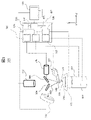
- FIG. 1 is an overall configuration diagram showing a configuration example of a sample scanning type scanning probe microscope according to an embodiment.
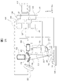
- FIG. 2 is an overall configuration diagram showing a configuration example of a probe scanning type scanning probe microscope according to an embodiment.
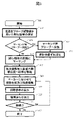
- FIG. 3 is a flow chart showing the procedure from the scanning probe microscope shown in FIGS. 1 and 2 to the same point observation or processing to the magnifying observation processing apparatus.
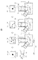
- FIG. 4 is a diagram illustrating configuration example 1 of the sample observation and processing system according to the embodiment.
- FIG. 5 is a diagram illustrating configuration example 2 of the sample observation and processing system according to the embodiment.
- FIG. 6 is a diagram illustrating configuration example 3 of the sample observation and processing system according to the embodiment.
- FIG. 7 is a diagram illustrating an example of arrangement of markers according to the embodiment.
- FIG. 1 is an overall configuration diagram showing a configuration example of a sample scanning type scanning probe microscope according to an embodiment.
- FIG. 2 is an overall configuration diagram showing a configuration example of a probe scanning type scanning probe microscope according to an embodiment
- FIG. 8 is a diagram illustrating an example of the shape of the marker according to the embodiment.
- FIG. 9 is a diagram for explaining positional deviation correction before and after exchanging the marking probe.
- FIG. 10 is a diagram illustrating configuration example 1 of a marking setting screen according to the embodiment.
- FIG. 11 is a diagram illustrating configuration example 2 of a marking setting screen according to the embodiment.
- FIG. 1 shows a configuration diagram of a sample scanning scanning probe microscope (SPM) 101 of this embodiment.
- the overall operation of scanning probe microscope 101 shown in FIG. The overall operation of scanning probe microscope 101 shown in FIG. Then, the probe 114 attached to the tip of the surface of the cantilever 108 is brought close to the surface of the sample 109 placed on the sample table 110 by driving the sample scanner Z piezo 111 .
- Laser diode 106 is driven by laser control circuit 120 to emit laser light 103 .
- the cantilever 108 warps due to the force acting between the probe 114 and the sample 109 , and the incident position of the laser beam 103 incident on the photodetector 102 via the detector-side mirror 104 changes.
- the change in the incident position is amplified by the signal amplifier circuit 123, and the sample scanner Z piezo 111 is rotated by the Z feedback circuit 124 so that the force acting between the probe 114 and the sample 109 is always maintained at a very small force.
- the sample scanner Z piezo 111 is expanded and contracted in the direction (vertical direction), and the voltage applied to the sample scanner Z piezo 111 is converted into height information by the signal processing unit 125 .
- the height information is stored in the storage unit 126 .
- the sample 109 is scanned in the X direction (horizontal direction) and the Y direction (back and forth direction) by the sample scanner X piezo 112 and the sample scanner Y piezo 113 driven by the XY piezo driving circuit 122, and the sample scanner Z piezo 111 is applied. Together with the voltage, it is converted into three-dimensional information by the signal processing unit 125 .
- the three-dimensional information is displayed on the monitor display unit 128 as an image of the field of view measured using the scanning probe microscope 101 .
- a method of scanning the sample 109 while vibrating the cantilever 108 by applying an AC signal from the bimorph piezo driving circuit 121 to the bimorph piezo 107 is also used.
- a coarse movement mechanism capable of manually or electrically moving either the cantilever 108 or the sample stage 110 is provided so that the relative position of the probe 114 and the sample 109 can be changed.
- the position is adjusted using an optical microscope 115 placed directly above the cantilever 108 .
- FIG. 2 shows a configuration diagram of the probe scanning scanning probe microscope 201 of this embodiment.
- a probe scanning scanning probe microscope (hereinafter sometimes abbreviated as SPM) 201 differs from the sample scanning scanning probe microscope 101 in that it has a probe scan Z piezo 211, a probe scan X piezo 212, and a probe scan Y piezo 213. is attached to the cantilever 108 side, and data is acquired by scanning the probe 114 .
- Other configurations and functions of the probe scanning scanning probe microscope 201 are the same as the configuration and functions of the sample scanning scanning probe microscope 101, and overlapping descriptions are omitted.
- a method is used in which all or part of the laser diode 106, the laser-side mirror 105, the detector-side mirror 104, and the photodetector 102 are scanned at the same time, and the laser beam 103 is synchronized with the scanning operation of the cantilever 108.
- the sample stage 214 can be driven manually or by a sample stage drive circuit 215 .
- FIG. 3 is a flow chart showing the procedure from the scanning probe microscope shown in FIGS. 1 and 2 to the magnifying observation and processing apparatus for performing the same point observation and/or processing. A method of implementing the present invention will now be described with reference to the flow diagram of FIG.
- step 301 the region of interest is measured using the scanning probe microscope (101 or 102).
- step 303 it is determined whether or not the measuring probe having the observation probe of the scanning probe microscope should be replaced with the marking probe having the marking probe.
- step 303 if the marking probe is to be replaced (Yes), the process proceeds to step 304 .
- step 303 when marking is performed with the measurement probe used to measure the region of interest, that is, when the measurement probe is also used as the marking probe (No), the process proceeds to step 306 .
- the probe When marking, the probe may be replaced with a marking probe in order to perform marking with high visibility. At that time, since the probe position may shift after the probe is replaced, as shown in step 305, the probe position shift is corrected by comparing the data obtained by scanning the optical microscope image or the sample surface. That is, when the scanning probe microscope (101 or 102) replaces the measuring probe with the marking probe, the positional deviation between the observing probe of the measuring probe and the marking probe of the marking probe is corrected. have the means to correct it.
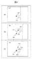
- FIG. 9 is a diagram for explaining positional deviation correction before and after exchanging the marking probe.
- FIG. 9 shows an example of positional deviation correction using an optical microscope image.
- 9(a), (b), and (c) all represent optical microscope images of an optical microscope 115 attached directly above the cantilever 108 of the scanning probe microscope (101 or 102).
- FIG. 9(a) shows an optical microscope image immediately after the region of interest is measured using the measurement probe 902.
- FIG. 9(b) shows an optical microscope image immediately after the marking probe 903 is replaced.
- FIG. 9(c) shows an optical microscope image when the measuring probe position 901 and the marking probe position 904 are aligned.
- the probe position 901 of the measurement probe is clicked with a pointing device such as a mouse. Then, the measurement probe position 901 is stored in the storage unit 126 .
- the marking probe position 904 is clicked with a pointing device on the optical microscope image immediately after the marking probe 903 is replaced, and the measuring probe position is A marking probe position shift distance 905, which is the distance between 901 and the marking probe position 904, is measured.
- the marking probe 903 and the marking probe 903 and The position relative to the sample 109 is moved. In this method, the marking probe 903 side and the sample 109 side may be moved. In FIG. It shows how the marking probe 903 side is moved diagonally downward to the left as indicated by the arrow so as to overlap with 901 .
- 906 represents the marking probe after misalignment correction.
- FIG. 7 is a diagram illustrating an example of marker arrangement by a scanning probe microscope (SPM) according to the embodiment.
- SPM scanning probe microscope
- Each marker shown in FIG. 7 suppresses deterioration of the region of interest due to narrow-area observation of the magnifying observation processing device, so that the position of the region of interest can be easily specified while maintaining the state of wide-area observation of the magnifying observation processing device. is established for the purpose of An arrangement example of each marker shown in (a) to (j) of FIG. 7 will be described below.
- the periphery of the region of interest corresponds to the outer edge of the region of the observation field of view (703) during marking search of the magnifying observation processing apparatus.
- a marker 705 is generated that indicates at least part of the outer edge of the area of the field of view 703 .
- the visual field aspect ratio of the observation visual field 703 of the magnifying observation processing apparatus is assumed to be 4:3.
- a bracket-shaped (L-shaped) marker 705 is generated to indicate at least one corner of the rectangle, which is a rectangle that matches or is similar to the observation field of view 703 during marker search of the magnifying observation processing apparatus.
- the center of the region of interest 702 is set as the center of rotation, such as the bracket-shaped marker 705, by arranging the marker at a position that is not rotationally symmetrical (non-rotationally symmetrical position), observation of the region of interest 702 and the magnifying observation processing apparatus can be performed.
- the angles of the field of view 703 can be matched.
- the arrangement shown in (d) of FIG. 7 is used.
- the arrangement of markings is arbitrary according to the arrangement of (f) in FIG. 7 and the aspect ratio of the observation field of view of the magnifying observation and processing device. is preferably settable.
- the scanning probe microscopes 101 and 102 can be summarized as follows.
- the scanning probe microscopes 101 and 102 have scanning units (for example, 111 to 113, 211 to 213, etc.) for relatively scanning the sample 109 and the probe 114, and scan the sample 109 and the probe 114.
- the sample 109 is observed by this.
- the scanning probe microscopes 101 and 102 each have a controller 127 .
- the control unit 127 is a magnifying observation and processing device for further observing and/or processing after acquiring the region of interest 702 obtained as a result of scanning.
- the area to be observed or processed by the magnifying observation processing device (for example, the field size of the observation field of view 703, the field aspect ratio, the field magnification, the observation angle, etc.) is determined.
- Control is performed so as to form a marker indicating the
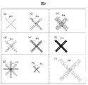
- FIG. 8 is a diagram illustrating an example of the shape of markers formed by the scanning probe microscope according to the example.
- an example of the shape of a cross-shaped (X-shaped) marker 704 is described as a representative example, but it is also applicable to the shapes of other markers (701, 705, 709, 710, 711).
- An example of the marker shape will be described with reference to (a) to (i) of FIG.
- FIG. 8 shows a single-line marker (single-line scratch mark) 801 formed on the sample 109 by a scratch mark of the probe 114 of the scanning probe microscope (101 or 102). If the visibility of the single-line marker 801 shown in FIG. 8(a) is not sufficient, a four-line marker 802 as shown in FIG. 8(b) and an eight-line marker 803 as shown in FIG. Thus, it is also possible to increase the number of lines to form a multi-line scratch mark and improve the visibility of the marker.
- FIG. 8(d) shows a weak contact pressure marker 811 when the scratch mark of the probe 114 of the scanning probe microscope (101 or 102) is attached to the sample 109 with a weak pressure.
- the scanning speed of the probe 114 with respect to the sample 109 is adjusted, and as shown in FIG. 812 can also be set.
- the probe 114 in order to deepen or thicken the scratch mark, the probe 114 is repeatedly scratched at the same position a plurality of times to form a deep scratch mark.
- the number of times of overwriting (for example, 3 times) can be set.
- a rice-shaped (asterisk-shaped) marker 821 with an increased number of scratches can also be set.
- the size of the marker itself can be set to any size depending on the situation, such as a small size marker 831 shown in FIG. 8(h) or a large size marker 832 shown in FIG. 8(i). .
- the shape of the marker may be distorted due to the characteristics of the piezoelectric element.
- the probe 114 is moved in the air or under conditions where the probe 114 does not mark the sample 109 (conditions where the probe 114 does not form a marker on the sample 109).
- the scanner (111 to 113 or 211 to 213) scans a plurality of times and the probe 114 scans a plurality of times, and then the sample 109 is marked by the probe 114. .
- the distortion of the shape of the marker can be reduced. Also, in this way, it is possible to set to reduce the distortion of the shape of the marker.
- FIG. 10 is a diagram showing configuration example 1 of a marking setting screen provided in the scanning probe microscope (SPM) according to the embodiment.
- SPM scanning probe microscope
- FIG. 10 as a representative example, a case where markers are formed at three corners of the observation field of view 703 (see, for example, (a) of FIG. 7) will be described. (h), (i), (l), (k), (j)).
- the marking setting screen 1001 is displayed on the monitor display unit 128.
- the marking setting screen 1001 has an SPM scanner movable range display section 1002 and a marking condition display section 1003 .
- An SPM observation field of view 1022 and a region of interest 1024 are displayed in the scanner movable range display unit 1002 , and the scanner coordinates of the region of interest 1024 are displayed at the region of interest position 1012 .
- the user selects the type of magnifying observation processing device in the marking condition display section 1003.
- the magnifying observation processing device one device can be selected from three devices: the first scanning electron microscope SEM1, the second scanning electron microscope SEM2, and the focused ion beam device FIB1.
- FIG. 10 shows a state in which the first scanning electron microscope SEM1 is selected (black circle ⁇ mark).
- the first scanning electron microscope SEM1 can be a device whose observation field of view has the same, higher, or lower magnification as compared to the second scanning electron microscope SEM2.
- the magnifying observation processing device (here, the selected first scanning electron microscope SEM1) previously registered by the user by clicking the observation field setting button 1004 or acquired by communication is displayed as a marker.
- the observation field of view 703 and the aspect ratio of the observation field of view 703 when searching for are read, and a marking position (marker's placement position conditions).
- the user selects or inputs a numerical value for the interval for arranging the markers from the marker spacing list box 1007, selects or inputs a numerical value for the marker shape from the marker shape list box 1005, and selects or inputs a numerical value for the size of the marker from the marker size list box 1006.
- 8(g) to 8(i) can be specified.
- the marking condition display section 1003 When these conditions are set in the marking condition display section 1003, the marking location 1021 based on the designated marking conditions and the observation field of view 1023 of the first scanning electron microscope SEM1, which is the magnifying observation processing device, are displayed in the scanner movable range display section 1002. , for example, as a dotted rectangle.
- the marking conditions set in the marking condition display section 1003 and the display image of the scanner movable range display section 1002 can be stored in the storage section 126, for example.
- the end button is clicked, the display of the marking setting screen 1001 ends.
- each condition described below may be set in the marking condition display section 1003 before marking is started.
- the user can select the number of marker lines from the marker number list box 1008 or enter a numerical value to specify the number of marker lines as shown in FIGS. 8(a) to 8(c).
- the user selects or inputs a numerical value for the pressing amount of the cantilever 108 (or the probe 114) during marker drawing from the drawing pressing amount list box 1009, and the marker drawing speed (cantilever 108 (or Select or enter a numerical value for the moving speed of the probe 114), select or enter a numerical value for the number of times the marker is overwritten from the number of times of overwriting list box 1011, and perform the operations shown in FIGS. 8(d) to 8(f).
- a condition for optimizing the visibility of the marker in the magnifying observation processing apparatus can be set in the marking condition display section 1003.
- FIG. 10 As a result, the visibility of the marker can be optimized, and the visibility of the marker can be improved.
- list boxes 1005 to 1011 for setting conditions for forming markers are provided in the marking condition display section 1003, the present invention is not limited to this. Marker forming conditions that can improve the visibility of the markers can be input or set in the marking condition display section 1003 .
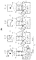
- FIG. 4 is a diagram illustrating configuration example 1 of the sample observation and processing system according to the embodiment.
- a sample observation and processing system 400 includes a scanning probe microscope (SPM) and a magnifying observation and processing device shown in FIG. 1 or 2 .
- FIG. 4 shows a sample observation and processing system 400 in which the magnifying observation and processing device is a scanning electron microscope (SEM).
- SPM scanning probe microscope
- SEM scanning electron microscope
- FIG. 4A shows three points around a region of interest 405 measured on the surface of a sample 402 placed on a sample stage 403 using a marking probe 401 of a scanning probe microscope (SPM).
- SPM scanning probe microscope
- step 307 of FIG. 3 the sample placed on the scanning probe microscope (SPM) is moved to the observation position of the magnifying observation processing device, and the state immediately after that is shown in FIG. 4(b).
- Incident electrons emitted from a column 411 of a scanning electron microscope (SEM) irradiate a sample 413 fixed on a sample stage 412 of the SEM, and secondary electrons and reflected electrons generated from near the irradiated area are detected by the SEM. It is detected by a device 414, processed by a signal processing unit 415 of the SEM, and an observation field of view 416 of the SEM is displayed on the monitor.
- SEM scanning electron microscope
- step 308 of FIG. 3 the field position and angle of the scanning electron microscope (SEM) are adjusted according to the markers, and the state after adjustment is shown in FIG. 4(c).
- the marker 404 is arranged at the viewing angle as shown in the observation viewing field 417 of the SEM after adjusting the viewing field position and angle.
- step 309 of FIG. 3 the field magnification of the scanning electron microscope (SEM) is increased to enlarge the observation field of view 418, and as in the SEM observation field of view 418 after enlargement in FIG. It can be displayed in the same size as the measurement field of view 406 of the probe microscope (SPM).
- SEM scanning electron microscope
- step 310 of FIG. 3 the region of interest 405 is observed and/or processed. If there is still another region of interest (Yes in step 311 of FIG. 3), the scanning electron microscope (SEM) is positioned at the marker provided around the next region of interest, as shown in step 311 of FIG. You can also move to the field of view position of the SEM) and repeat the observation of the next region of interest. When all regions of interest have been observed (No in step 311 of FIG. 3), the process proceeds to step 312 of FIG. 3, and the flowchart of FIG. 3 ends.
- SEM scanning electron microscope
- FIG. 5 is a diagram illustrating configuration example 2 of the sample observation and processing system according to the embodiment.
- a sample observation and processing system 500 includes a scanning probe microscope (SPM) and a magnifying observation and processing device shown in FIG. 1 or 2 .
- FIG. 5 shows a sample observation and processing system 500 in which the magnifying observation and processing apparatus is a scanning electron microscope/focused ion beam combined machine (FIB-SEM).
- FIB-SEM scanning electron microscope/focused ion beam combined machine
- Fig. 5 shows the case where the sample is moved from the scanning probe microscope (SPM) to the scanning electron microscope/focused ion beam combination machine (FIB-SEM), and the same location in the region of interest is observed and/or processed. .
- a region of interest 405 in a scanning probe microscope (SPM) is specified, and three markers 404 are formed around the region of interest 405 .
- the sample 513 having the three-point markers 404 formed thereon is placed on the sample stage 512 of the FIB-SEM, as shown in FIG. 5(b).
- Incident electrons emitted from a column 511 of a scanning electron microscope (SEM) irradiate a sample 513 fixed on a sample stage 512 of the FIB-SEM, and secondary electrons and reflected electrons generated from the vicinity of the irradiation part are emitted by the FIB. It is detected by the detector 514 of the -SEM, processed by the signal processing unit 515 of the FIB-SEM, and the observation field of view 516 of the FIB-SEM is displayed on the monitor.
- FIG. 5(c) shows the state after adjusting the visual field position and angle according to the marker.
- the marker 405 is arranged at the viewing angle as shown in the observation viewing field 518 of the FIB-SEM after adjusting the viewing field position and angle.
- the observation field of view 518 of the FIB-SEM can be enlarged and displayed in the same size as the measurement field of view 406 of the SPM, like the FIB-SEM observation field of view 519 after enlargement in FIG. 5(d). can.
- the region of interest 405 can then be observed and/or processed by a beam of ions emitted from column 517 of a focused ion beam device (FIB).
- FIB focused ion beam device
- FIG. 6 is a diagram illustrating configuration example 3 of the sample observation and processing system according to the embodiment.
- a sample observation and processing system 600 includes a scanning probe microscope and a magnifying observation and processing device.
- the scanning probe microscope is a scanning probe microscope/scanning electron microscope (SPM-SEM) complex machine
- the magnifying observation processing device is a scanning electron microscope/focused ion beam (FIB-SEM) complex machine. shows a sample observation and processing system 600.
- SPM-SEM scanning probe microscope/scanning electron microscope
- FIB-SEM scanning electron microscope/focused ion beam
- FIG. 6 shows a scanning probe microscope/scanning electron microscope (SPM-SEM) combination machine in which one or more scanning probe microscopes are installed in a charged particle beam device (scanning electron microscope in this example).
- the sample is moved to an electron microscope/focused ion beam (FIB-SEM) combination machine, and the same part in the region of interest is observed and/or processed.
- One or more conductive probes 607 and scanning probe microscope (SPM) marking probes 603 are arranged around the sample 402 in the sample chamber of the scanning probe microscope/scanning electron microscope (SPM-SEM) composite machine. be.
- a conductive probe 607 is provided for electrical measurement purposes.
- a scanning probe microscope/scanning electron microscope (SPM-SEM) composite machine uses these probes 607 and 603 to scan a sample 402, and to scan an ammeter 608 and a constant voltage source while fixed at a specific position. 609 to evaluate the electrical characteristics of a fine semiconductor element formed on the sample 402 and to form markers 404 around the region of interest 405 .
- the scanning probe microscope/scanning electron microscope (SPM-SEM) composite machine includes a microsemiconductor element characterization device.
- Fig. 6 (a) shows the configuration diagram of the SPM-SEM composite machine.
- Incident electrons emitted from the column 602 of the scanning electron microscope (SEM) of the SPM-SEM composite machine irradiate the sample 402 fixed on the specimen stage 604 of the SPM-SEM composite machine, and two electrons are generated near the irradiation part. Secondary electrons and backscattered electrons are detected by a detector 605 of the SPM-SEM complex machine, processed by a signal processing unit 606 of the SPM-SEM complex machine, and an observation field 601 of the SPM-SEM complex machine is displayed on the monitor.
- SEM scanning electron microscope
- FIG. 6 In the field of view 601 of the SPM-SEM composite machine, the positions of the region of interest 405 and the marker 404, and the movements and fixed positions of the conductive probe 607 and the marking probe 603 are displayed.
- a marker 404 is formed around the specified region of interest 405 of the sample 402 using a marking probe 603 installed inside the SPM-SEM complex machine, and then the sample 402 with the marker 404 formed thereon is subjected to FIB- It is moved to the sample stage 512 of the SEM multifunction device, and the region of interest 405 is observed and/or processed.
- (b), (c), and (d) of FIG. 6 are the same as (b), (c), and (d) of FIG. 5, and redundant explanations are omitted.
- FIG. 6 it is also possible to construct a sample observation and processing system 600.
- FIG. 6 it is also possible to construct a sample observation and processing system 600.
- the scanning probe microscope/scanning electron microscope (SPM-SEM) combined machine will be further explained.
- the combined scanning probe microscope/scanning electron microscope (SPM-SEM) incorporates the function of an electrical property evaluation device that evaluates the electrical properties of the sample 402 .
- the conductive probe 607 can be said to be a conductive probe.
- the scanning probe microscope/scanning electron microscope (SPM-SEM) combined machine has a driving unit (111- 113 or 211 to 213), an electrical property evaluation unit (608, 609) connected to a probe 607 for evaluating the electrical property of the sample 402, and a charged particle beam for irradiating the sample 402 with a charged particle beam. and an irradiation unit 602 .
- a scanning probe microscope/scanning electron microscope (SPM-SEM) composite machine evaluates the electrical characteristics of the sample 402 by irradiating the sample 402 with a charged particle beam while keeping the probe 607 in contact with the sample 402 .
- the probe 607 of the scanning probe microscope/scanning electron microscope (SPM-SEM) composite machine can contact the sample 402 within the field of view of the charged particle beam irradiation unit 602, and the probe 607 is brought into contact with the sample 402.
- the electrical characteristics of the sample 402 are evaluated by irradiating the sample 402 with the charged particle beam while the sample 402 is being measured.
- the electrical characteristics of the sample 402 are evaluated by measuring, through the probe 607, the current and/or voltage generated in the semiconductor elements and wirings formed on the sample 402 by irradiation with the charged particle beam.
- the scanning probe microscope/scanning electron microscope (SPM-SEM) composite machine identifies a region of interest 405 of the sample 402 based on the results of the electrical property evaluation.
- the region of interest 405 includes, for example, a region including a disconnected portion of wiring, a region including a defective portion of a semiconductor element or wiring, a region including a foreign matter portion on the sample 402, a portion that satisfies or does not satisfy a predetermined condition, and the like. It can be a region or the like.
- the scanning probe microscope/scanning electron microscope (SPM-SEM) combined machine is an area that includes the region of interest 405, and is at the center of scaling when the area is observed with a magnifying observation processing device (FIB-SEM).
- FIB-SEM magnifying observation processing device
- FIG. 11 is a diagram illustrating configuration example 2 of a marking setting screen according to the embodiment.
- FIG. 11 differs from FIG. 10 in that an observation field setting area 1104 is provided in the marking condition display section 1003 instead of the observation field setting button 1004, and a selectable marking position designation section 1121 for designating a marking position. is displayed in the scanner movable range display section 1002, and the observation field of view 1123 and the marking point designation section 1121 of the magnifying observation processing apparatus set in the observation field setting area 1104 are displayed on the scanning probe microscope (SPM ) is superimposed on the image 1110 obtained by ) and displayed in the scanner movable range display unit 1002 .
- SPM scanning probe microscope
- Other configurations and functions in FIG. 11 are the same as other configurations and functions in FIG. 10, so overlapping descriptions will be omitted.
- FIG. 11 shows a state in which a template is selected (black circle ⁇ mark).
- detail selection area 1105 is displayed.
- the detailed selection area 1105 is configured to display options related to the field magnification of the magnifying observation processing device (here, the first scanning electron microscope SEM1) selected in the destination observation device.
- a template item with a magnification of x10k and a template item with a magnification of x5k are shown as representative examples for the first scanning electron microscope SEM1, and the template item with a magnification of x10k is selected (check mark ).
- the observation field of view 1123 of the first scanning electron microscope SEM1 corresponding to the aspect ratio is displayed in the scanner movable range display section 1002. be done.
- marking location designating portions 1121 are displayed at four corners of the observation field of view 1123 .
- the marking location specifying section 1121 is configured to be selectable.
- three corner marking location designation portions 1121 are in a selected state (ticks).
- marker placement positions can be specified at three corners around the region of interest 1024 .
- Marker shapes and the like are set by setting list boxes 1005 to 1011 for setting conditions. After setting the template items, selecting the marking location designation part 1121, and setting the condition setting list boxes 1005 to 1011, clicking the marking start button causes three corners around the region of interest 1024 to be marked. Highly visible markers can be formed automatically.
- the template item is the template item of magnification, but it may be the aspect ratio of the observation field.
- the detail selection area 1105 may be configured so that the field magnification or field aspect ratio at the time of marker search of the magnifying observation processing apparatus can be input.
- the user can specify the placement position of the marker while visually confirming the image 1110 displayed in the scanner movable range display section 1002 and the marking location specifying section 1121, thereby providing an interface with improved convenience for the user. can.
- an observation field of view 1124 shown in the scanner movable range display section 1002 exemplifies the observation field of view of the second scanning electron microscope SEM2.
- the image 1110 may be an image obtained with the optical microscope 115 of the scanning probe microscope (SPM) of FIG. 1 or FIG.
- control unit 127 can perform calculations based on the values input to the predetermined items, and can cause the scanner movable range display unit 1002 to display the same as in FIG.
- the marking location designating portion 1121 indicates the location where the marker will be formed, and the observation field of view 1123 indicates the observation field of view of the first scanning electron microscope SEM1. is.
- FIG. 11 it is also possible to configure so that the sides between the marking location specifying portions 1121 can be selected.
- the markers of the sides 709, 710, and 711 shown in (i), (k), and (j) of FIG. 7 can be formed in a shape with improved visibility.
- 101 sample scanning scanning probe microscope (SPM), 102: photodetector, 103: laser light, 104: detector side mirror, 105: laser side mirror, 106: laser diode, 107: bimorph piezo, 108: cantilever, 109: Sample, 110: Sample stage, 111: Sample scanner Z piezo, 112: Sample scanner X piezo, 113: Sample scanner Y piezo, 114: Probe, 115: Optical microscope, 120: Laser control circuit, 121: Bimorph drive circuit, 122: XY piezo drive circuit, 123: signal amplifier circuit, 124: Z feedback circuit, 125: signal processing unit, 126: storage unit, 127: control unit, 128: monitor display unit, 201: probe scan type scanning probe microscope (SPM), 211: probe scanner Z piezo, 212: probe scanner X piezo, 213: probe scanner Y piezo, 214: sample stage, 215: sample stage drive circuit, 401: marking probe, 402: sample,
Landscapes
- Physics & Mathematics (AREA)
- Health & Medical Sciences (AREA)
- General Health & Medical Sciences (AREA)
- General Physics & Mathematics (AREA)
- Nuclear Medicine, Radiotherapy & Molecular Imaging (AREA)
- Radiology & Medical Imaging (AREA)
- Chemical & Material Sciences (AREA)
- Engineering & Computer Science (AREA)
- Nanotechnology (AREA)
- Analytical Chemistry (AREA)
- Analysing Materials By The Use Of Radiation (AREA)
- Sampling And Sample Adjustment (AREA)
- Testing Of Individual Semiconductor Devices (AREA)
Abstract
Description
本実施例では、基本的な実施形態について説明する。図1は、本実施例のサンプルスキャン方式走査型プローブ顕微鏡(SPM)101の構成図を示す。
図3は、図1、図2に示す走査型プローブ顕微鏡から拡大観察加工装置への同一箇所観察または加工またはその両方を行うまでの手順を示すフローチャートである。図3のフロー図を参照しながら、本発明の実施方法を説明する。
Claims (13)
- 試料と探針を相対的に走査するための走査部を有し、前記試料と前記探針を走査することにより前記試料を観察する走査型プローブ顕微鏡であって、
制御部を備え、
前記制御部は、前記走査の結果得られる関心領域を取得したのちに、さらに観察または加工またはその両方を行うための拡大観察加工装置であって、当該走査型プローブ顕微鏡とは別個の前記拡大観察加工装置に関する情報を元に、前記拡大観察加工装置が観察または加工する領域が前記関心領域を内包する領域であり、かつ、当該領域を前記拡大観察加工装置で観察した際の拡大縮小中心に前記関心領域が位置する観察または加工する領域を特定し、前記探針と前記試料を相互作用させることにより、前記観察または加工する領域の外縁の少なくとも一部を示すマーカーを形成するように、制御を行う、走査型プローブ顕微鏡。 - 請求項1に記載の走査型プローブ顕微鏡であって、
前記マーカーは、前記探針と前記試料の相互作用によって形成され、
前記マーカーを形成する位置は、前記拡大観察加工装置が前記マーカーを探索するときの視野サイズと一致もしくは相似の矩形であって、前記矩形の少なくとも1つの角部または辺を示すように生成される、走査型プローブ顕微鏡。 - 請求項1又は2に記載の走査型プローブ顕微鏡であって、
前記マーカーは前記関心領域の中心を回転中心としたときに回転対称ではない位置に配置される、走査型プローブ顕微鏡。 - 請求項1乃至3のいずれか一項に記載の走査型プローブ顕微鏡であって、
前記拡大観察加工装置のマーカー探索時の視野サイズもしくは視野アスペクト比を記憶し、前記視野サイズに合ったマーカーの配置位置条件を選択し、制御することができる、走査型プローブ顕微鏡。 - 請求項1乃至4のいずれか一項に記載の走査型プローブ顕微鏡であって、
前記マーカーが線で構成される際に、マーカー線の方向、前記マーカー線の長さ、前記マーカー線の太さ、前記マーカー線の重ね書き回数、前記マーカー線の深さもしくは高さ、前記マーカー線の描画速度のいずれか一つ以上の条件を変えることができる、走査型プローブ顕微鏡。 - 請求項1乃至5のいずれか一項に記載の走査型プローブ顕微鏡であって、
前記走査部が圧電素子より構成され、
前記マーカーを形成する際に、空中もしくは前記探針により前記試料にマーカーが形成されないほどの条件において、複数回の走査を行った後に、所定の前記マーカーを形成する、走査型プローブ顕微鏡。 - 請求項1乃至6のいずれか一項に記載の走査型プローブ顕微鏡であって、
前記走査型プローブ顕微鏡は観察用探針とマーキング用探針を交換又は併用可能であり、前記観察用探針と前記マーキング用探針の位置ずれを補正する手段を有する、走査型プローブ顕微鏡。 - 請求項1に記載の走査型プローブ顕微鏡であって、
モニタ表示部を有し、
前記モニタ表示部は、スキャナ可動範囲表示部とマーキング条件表示部とを含むマーキング設定画面と表示し、
前記マーキング設定画面は、前記拡大観察加工装置のマーカー探索時の視野倍率もしくは視野アスペクト比を入力可能に構成され、
前記視野倍率もしくは前記視野アスペクト比が前記マーキング条件表示部に入力されたことに基づいて、前記スキャナ可動範囲表示部は前記拡大観察加工装置が前記マーカーを探索するときの視野サイズと一致もしくは相似の矩形を表示し、かつ、前記矩形の角部に選択可能なマーキング箇所指定部を表示し、
前記マーキング箇所指定部の選択状態に基づいて、前記マーカーが前記試料に形成される、走査型プローブ顕微鏡。 - 請求項1乃至8のいずれか一項に記載の走査型プローブ顕微鏡と、前記関心領域が特定された前記試料をさらに観察または加工またはその両方を行うための拡大観察加工装置と、を備える、試料観察加工システムであって、
前記試料観察加工システムは、前記走査型プローブ顕微鏡により生成された前記マーカーを用いて、前記走査型プローブ顕微鏡の前記関心領域と前記拡大観察加工装置の観察または加工する領域の角度を合わせるように、前記拡大観察加工装置の視野のいずれか1つ以上の角と、前記マーカーとを一致させたのち、前記拡大観察加工装置の倍率を上昇させ、前記関心領域の観察または加工またはその両方を実行する、試料観察加工システム。 - 請求項9に記載の試料観察加工システムであって、
走査電子顕微鏡の試料室内に試料の電気測定を目的とした導電性プローブまたは前記走査型プローブ顕微鏡が一つまたは複数設置されており、前記導電性プローブもしくは前記走査型プローブ顕微鏡もしくはその両方によって前記関心領域を特定し、前記マーカーを形成することができる、試料観察加工システム。 - 試料の電気特性を評価する電気特性評価装置であって、
導電性の探針と、
前記試料と前記探針の相対的な位置関係を変更させる駆動部と、
前記探針に接続され、前記試料の電気特性を評価する電気特性評価部と、
前記試料に向けて荷電粒子線を照射する荷電粒子線照射部と、
を備え、
前記探針を前記試料に接触させながら前記荷電粒子線を前記試料に照射することにより前記試料の電気特性を評価し、前記評価の結果に基づき関心領域を特定し、
前記関心領域を内包する領域であり、かつ、当該領域を拡大観察加工装置で観察した際の拡大縮小中心に前記関心領域が位置する、観察または加工する領域を特定し、
前記探針と前記試料を相互作用させることにより、前記観察または加工する領域の外縁の少なくとも一部を示すマーカーを形成する、
電気特性評価装置。 - 試料の電気特性を評価する電気特性評価装置であって、
導電性の探針と、
前記試料と前記探針の相対的な位置関係を変更させる駆動部と、
前記探針に接続され、前記試料の電気特性を評価する電気特性評価部と、
前記試料に向けて荷電粒子線を照射する荷電粒子線照射部と、
を備え、
前記探針は、前記荷電粒子線照射部の視野内において前記試料と接触可能であり、
前記探針を前記試料に接触させながら前記荷電粒子線を前記試料に照射することにより前記試料の電気特性を評価し、前記評価の結果に基づき関心領域を特定し、
前記関心領域を内包する領域であり、かつ、当該領域を拡大観察加工装置で観察した際の拡大縮小中心に前記関心領域が位置する、観察または加工する領域を特定し、
前記探針と前記試料を相互作用させることにより、前記観察または加工する領域の外縁の少なくとも一部を示すマーカーを形成する、
電気特性評価装置。 - 請求項11又は12に記載の電気特性評価装置と、
前記電気特性評価装置により電気特性が評価された前記試料の前記関心領域について観察若しくは加工又はその両方を行うための拡大観察加工装置と、
を備える、試料観察加工システム。
Priority Applications (5)
| Application Number | Priority Date | Filing Date | Title |
|---|---|---|---|
| JP2023508358A JP7556132B2 (ja) | 2021-03-26 | 2021-03-26 | 走査型プローブ顕微鏡、試料観察加工システムおよび電気特性評価装置 |
| PCT/JP2021/012775 WO2022201478A1 (ja) | 2021-03-26 | 2021-03-26 | 走査型プローブ顕微鏡、試料観察加工システムおよび電気特性評価装置 |
| KR1020237031582A KR20230147143A (ko) | 2021-03-26 | 2021-03-26 | 주사형 프로브 현미경, 시료 관찰 가공 시스템 및 전기 특성 평가 장치 |
| US18/283,932 US20240168052A1 (en) | 2021-03-26 | 2021-03-26 | Scanning Probe Microscope, Sample Observation Processing System, and Electric Characteristic Evaluation Device |
| TW111109553A TWI815352B (zh) | 2021-03-26 | 2022-03-16 | 掃描型探針顯微鏡、試料觀察加工系統及電特性評估裝置 |
Applications Claiming Priority (1)
| Application Number | Priority Date | Filing Date | Title |
|---|---|---|---|
| PCT/JP2021/012775 WO2022201478A1 (ja) | 2021-03-26 | 2021-03-26 | 走査型プローブ顕微鏡、試料観察加工システムおよび電気特性評価装置 |
Publications (1)
| Publication Number | Publication Date |
|---|---|
| WO2022201478A1 true WO2022201478A1 (ja) | 2022-09-29 |
Family
ID=83396658
Family Applications (1)
| Application Number | Title | Priority Date | Filing Date |
|---|---|---|---|
| PCT/JP2021/012775 Ceased WO2022201478A1 (ja) | 2021-03-26 | 2021-03-26 | 走査型プローブ顕微鏡、試料観察加工システムおよび電気特性評価装置 |
Country Status (5)
| Country | Link |
|---|---|
| US (1) | US20240168052A1 (ja) |
| JP (1) | JP7556132B2 (ja) |
| KR (1) | KR20230147143A (ja) |
| TW (1) | TWI815352B (ja) |
| WO (1) | WO2022201478A1 (ja) |
Families Citing this family (1)
| Publication number | Priority date | Publication date | Assignee | Title |
|---|---|---|---|---|
| CN121522430B (zh) * | 2026-01-15 | 2026-04-21 | 芯火微测(成都)科技有限公司 | 一种芯片倒置检测微光显微镜 |
Citations (7)
| Publication number | Priority date | Publication date | Assignee | Title |
|---|---|---|---|---|
| JP2002340756A (ja) * | 2001-05-11 | 2002-11-27 | Kansai Tlo Kk | 位置決めマーカおよび位置決め装置 |
| US20060270067A1 (en) * | 2005-05-27 | 2006-11-30 | Kun Lin | Defect Detection Method |
| JP2011064514A (ja) * | 2009-09-16 | 2011-03-31 | Fuji Electric Holdings Co Ltd | 走査型プローブ顕微鏡及び表面検査方法 |
| JP2012242146A (ja) * | 2011-05-17 | 2012-12-10 | Hitachi High-Technologies Corp | 走査電子顕微鏡及び試料作成方法 |
| JP2013114854A (ja) * | 2011-11-28 | 2013-06-10 | Hitachi High-Technologies Corp | 試料観察装置及びマーキング方法 |
| JP2017201304A (ja) * | 2016-04-08 | 2017-11-09 | カール・ツァイス・エスエムティー・ゲーエムベーハー | フォトリソグラフィマスクまたはウェハの欠陥を分析するためのデバイスおよび方法 |
| WO2019155518A1 (ja) * | 2018-02-06 | 2019-08-15 | 株式会社 日立ハイテクノロジーズ | 半導体装置の評価装置 |
Family Cites Families (4)
| Publication number | Priority date | Publication date | Assignee | Title |
|---|---|---|---|---|
| US6005400A (en) * | 1997-08-22 | 1999-12-21 | Lockheed Martin Energy Research Corporation | High resolution three-dimensional doping profiler |
| US6827979B2 (en) * | 1999-01-07 | 2004-12-07 | Northwestern University | Methods utilizing scanning probe microscope tips and products therefor or produced thereby |
| JP3819230B2 (ja) | 2000-10-31 | 2006-09-06 | シャープ株式会社 | マルチプローブ型走査プローブ顕微鏡装置およびそれを用いた試料表面評価方法 |
| JP7001494B2 (ja) * | 2018-02-26 | 2022-01-19 | 株式会社日立ハイテク | ウェハ観察装置 |
-
2021
- 2021-03-26 JP JP2023508358A patent/JP7556132B2/ja active Active
- 2021-03-26 KR KR1020237031582A patent/KR20230147143A/ko active Pending
- 2021-03-26 WO PCT/JP2021/012775 patent/WO2022201478A1/ja not_active Ceased
- 2021-03-26 US US18/283,932 patent/US20240168052A1/en active Pending
-
2022
- 2022-03-16 TW TW111109553A patent/TWI815352B/zh active
Patent Citations (7)
| Publication number | Priority date | Publication date | Assignee | Title |
|---|---|---|---|---|
| JP2002340756A (ja) * | 2001-05-11 | 2002-11-27 | Kansai Tlo Kk | 位置決めマーカおよび位置決め装置 |
| US20060270067A1 (en) * | 2005-05-27 | 2006-11-30 | Kun Lin | Defect Detection Method |
| JP2011064514A (ja) * | 2009-09-16 | 2011-03-31 | Fuji Electric Holdings Co Ltd | 走査型プローブ顕微鏡及び表面検査方法 |
| JP2012242146A (ja) * | 2011-05-17 | 2012-12-10 | Hitachi High-Technologies Corp | 走査電子顕微鏡及び試料作成方法 |
| JP2013114854A (ja) * | 2011-11-28 | 2013-06-10 | Hitachi High-Technologies Corp | 試料観察装置及びマーキング方法 |
| JP2017201304A (ja) * | 2016-04-08 | 2017-11-09 | カール・ツァイス・エスエムティー・ゲーエムベーハー | フォトリソグラフィマスクまたはウェハの欠陥を分析するためのデバイスおよび方法 |
| WO2019155518A1 (ja) * | 2018-02-06 | 2019-08-15 | 株式会社 日立ハイテクノロジーズ | 半導体装置の評価装置 |
Also Published As
| Publication number | Publication date |
|---|---|
| TWI815352B (zh) | 2023-09-11 |
| JPWO2022201478A1 (ja) | 2022-09-29 |
| TW202238135A (zh) | 2022-10-01 |
| JP7556132B2 (ja) | 2024-09-25 |
| US20240168052A1 (en) | 2024-05-23 |
| KR20230147143A (ko) | 2023-10-20 |
Similar Documents
| Publication | Publication Date | Title |
|---|---|---|
| US5081353A (en) | Combined scanning electron and scanning tunnelling microscope apparatus and method | |
| JP6009862B2 (ja) | 走査型プローブ顕微鏡 | |
| US9081028B2 (en) | Scanning probe microscope with improved feature location capabilities | |
| JP5164598B2 (ja) | レビュー方法、およびレビュー装置 | |
| US8887311B1 (en) | Scanning probe microscope | |
| JP2006105960A (ja) | 試料検査方法及び試料検査装置 | |
| JP5296578B2 (ja) | 電子顕微鏡の自動試料傾斜装置 | |
| CN101395676B (zh) | 带扫描探针显微镜的测量系统的操作方法及测量系统 | |
| JP2002350320A (ja) | 走査型プローブ顕微鏡 | |
| US5155359A (en) | Atomic scale calibration system | |
| JP3333148B2 (ja) | 外観検査装置 | |
| JPWO2017033591A1 (ja) | 荷電粒子線装置および試料ステージのアライメント調整方法 | |
| JP3970656B2 (ja) | 透過電子顕微鏡による試料観察方法 | |
| JP2803831B2 (ja) | 走査電子顕微鏡 | |
| JP7556132B2 (ja) | 走査型プローブ顕微鏡、試料観察加工システムおよび電気特性評価装置 | |
| JPH1027833A (ja) | 異物分析方法 | |
| JP5315076B2 (ja) | 電子線の影響を考慮した半導体検査方法及び装置 | |
| US7129727B2 (en) | Defect inspecting apparatus | |
| JP5191265B2 (ja) | 光学顕微鏡装置及び光学顕微鏡用データ処理装置 | |
| JP5491817B2 (ja) | 電子顕微鏡における薄膜試料位置認識装置 | |
| JP3560095B2 (ja) | 走査型プローブ顕微鏡 | |
| JPH09265931A (ja) | 画像取得装置及び方法 | |
| JP2003315238A (ja) | 測定位置合わせ方法、カンチレバ及び走査形プローブ顕微鏡 | |
| JP2004271270A (ja) | パターン検査方法及びパターン検査装置 | |
| JP3870141B2 (ja) | 電子顕微鏡 |
Legal Events
| Date | Code | Title | Description |
|---|---|---|---|
| 121 | Ep: the epo has been informed by wipo that ep was designated in this application |
Ref document number: 21933083 Country of ref document: EP Kind code of ref document: A1 |
|
| ENP | Entry into the national phase |
Ref document number: 20237031582 Country of ref document: KR Kind code of ref document: A |
|
| WWE | Wipo information: entry into national phase |
Ref document number: 1020237031582 Country of ref document: KR |
|
| WWE | Wipo information: entry into national phase |
Ref document number: 2023508358 Country of ref document: JP |
|
| WWE | Wipo information: entry into national phase |
Ref document number: 18283932 Country of ref document: US |
|
| NENP | Non-entry into the national phase |
Ref country code: DE |
|
| 122 | Ep: pct application non-entry in european phase |
Ref document number: 21933083 Country of ref document: EP Kind code of ref document: A1 |