WO2022190702A1 - レベルシフト回路及び電子機器 - Google Patents
レベルシフト回路及び電子機器 Download PDFInfo
- Publication number
- WO2022190702A1 WO2022190702A1 PCT/JP2022/003479 JP2022003479W WO2022190702A1 WO 2022190702 A1 WO2022190702 A1 WO 2022190702A1 JP 2022003479 W JP2022003479 W JP 2022003479W WO 2022190702 A1 WO2022190702 A1 WO 2022190702A1
- Authority
- WO
- WIPO (PCT)
- Prior art keywords
- level
- voltage
- shift circuit
- voltage level
- input signal
- Prior art date
- Legal status (The legal status is an assumption and is not a legal conclusion. Google has not performed a legal analysis and makes no representation as to the accuracy of the status listed.)
- Ceased
Links
Images



Classifications
-
- H—ELECTRICITY
- H03—ELECTRONIC CIRCUITRY
- H03K—PULSE TECHNIQUE
- H03K19/00—Logic circuits, i.e. having at least two inputs acting on one output; Inverting circuits
- H03K19/0175—Coupling arrangements; Interface arrangements
- H03K19/0185—Coupling arrangements; Interface arrangements using field effect transistors only
Definitions
- Embodiments according to the present disclosure relate to level shift circuits and electronic devices.
- the level shift circuit outputs a signal obtained by converting the voltage level of the input signal.
- the use of a cross-couple configuration is known (see, for example, Patent Document 1).
- the cross-couple configuration has a problem of increased power consumption because a through current flows at the timing when the voltage level of the input signal changes.
- the present disclosure provides a level shift circuit and an electronic device capable of reducing power consumption.
- two transistors of different conductivity types cascoded between two reference voltages having different voltage levels; a signal input unit that supplies an input signal having a high-level or low-level voltage level through a capacitor to at least one of two control terminals of the two transistors, respectively; and an impedance section for biasing the voltage level of the control terminal to which the input signal is supplied via the capacitor to a predetermined voltage level.
- the impedance section may be biased based on the voltage level of the reference voltage of the transistor having the control terminal to which the input signal is supplied via the capacitor.
- the impedance section is provided between the control terminal to which the input signal is supplied via the capacitor and the reference voltage of the transistor having the control terminal to which the input signal is supplied via the capacitor. may be connected.
- the impedance section may have an impedance equal to or higher than a predetermined value.
- the two transistors are a first transistor on the first reference voltage side; a second transistor on a second reference voltage side having a voltage level different from the first reference voltage;
- the signal input section supplies the input signal to a first control terminal of the first transistor through the capacitor and supplies the input signal to a second control terminal of the second transistor without the capacitor. death,
- the impedance section may bias the voltage level of the first control terminal to a predetermined voltage level.
- Either the high level or the low level of the input signal may be the same as the voltage level of either the first reference voltage or the second reference voltage.
- the two transistors are a first transistor on the first reference voltage side; a second transistor on a second reference voltage side having a voltage level different from the first reference voltage;
- the signal input section supplies the input signal to a first control terminal of the first transistor via a first capacitor, and the second control terminal of the second transistor via a second capacitor different from the first capacitor. supplying the input signal to a control terminal;
- the impedance section is a first impedance unit that biases the voltage level of the first control terminal to a predetermined voltage level; and a second impedance section for biasing the voltage level of the second control terminal to a predetermined voltage level.
- the high level and low level of the input signal may be different from the voltage levels of the first reference voltage and the second reference voltage.
- the first reference voltage and the second reference voltage may be a positive voltage and a negative voltage, respectively, or may be a negative voltage and a positive voltage, respectively.
- a signal output unit connected between the two cascode-connected transistors for outputting an output signal obtained by converting the voltage level of the input signal; a high impedance detection unit that detects that the signal output unit is high impedance; A logic fixer that fixes the voltage level of the output signal to one of the two reference voltages when the signal output section has a high impedance.
- a signal output unit connected between the two cascode-connected transistors for outputting an output signal obtained by converting the voltage level of the input signal; a level detection unit that detects the voltage level of at least one of the input signal and the two control terminals; When the voltage level of the input signal and at least one of the two control terminals continues at a high level or a low level for a predetermined period or longer, the voltage level of the output signal is set to either one of the two reference voltages. and a logic fixer that fixes the level.
- the impedance section may be a transistor whose control terminal is connected to one of the two reference voltages.
- the impedance unit is a diode, the anode of the diode is electrically connected to the lower voltage side of the two reference voltages; A cathode of the diode may be electrically connected to a higher voltage side of the two reference voltages.
- the impedance unit is a resistive element
- the resistance element may have a resistance value corresponding to the operating frequency of the level shift circuit and the capacitance of the capacitor.
- the resistance element may have a resistance value such that a cutoff frequency of a high-pass filter of the resistance element and the capacitor is lower than an operating frequency of the level shift circuit.
- It may further include a logic inverting section that supplies the input signal with its high level and low level inverted to each of the two control terminals.
- the voltage level of the input signal may alternately become high level or low level according to time.
- a DAC Digital to Analog Converter
- the level shift circuit is two transistors of different conductivity types cascoded between two reference voltages having different voltage levels; a signal input unit that supplies an input signal having a high-level or low-level voltage level through a capacitor to at least one of two control terminals of the two transistors, respectively; and an impedance section that biases the voltage level of the control terminal to which the input signal is supplied via the capacitor to a predetermined voltage level.
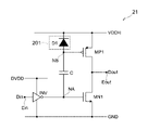
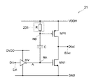
- FIG. 2 is a circuit diagram showing an example of the configuration of a first level shift circuit in the first embodiment
- FIG. 4 is a timing chart showing an example of the operation of the first level shift circuit in the first embodiment
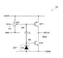
- 4 is a circuit diagram showing an example of the configuration of a second level shift circuit in the first embodiment
- FIG. 4 is a timing chart showing an example of the operation of the second level shift circuit in the first embodiment
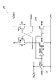
- FIG. 4 is a circuit diagram showing an example of a configuration of a first level shift circuit in a comparative example
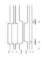
- 7 is a timing chart showing an example of the operation of the first level shift circuit in the comparative example
- It is a circuit diagram showing an example of the configuration of a first level shift circuit in the second embodiment.
- It is a circuit diagram showing an example of the configuration of a second level shift circuit in the second embodiment.
- It is a circuit diagram showing an example of the configuration of a first level shift circuit in the third embodiment.
- FIG. 11 is a circuit diagram showing an example of the configuration of a level shift circuit according to a fourth embodiment
- FIG. FIG. 11 is a circuit diagram showing an example of the configuration of a level shift circuit according to a fifth embodiment;
- FIG. 14 is a circuit diagram showing an example of a configuration of a first level shift circuit in a sixth embodiment;
- FIG. FIG. 14 is a circuit diagram showing an example of a configuration of a first level shift circuit in a seventh embodiment;
- level shift circuit and an electronic device will be described below with reference to the drawings.
- the main components of the level shift circuit and the electronic device will be mainly described below, the level shift circuit and the electronic device may have components and functions that are not illustrated or described. The following description does not exclude components or features not shown or described.
- FIG. 1 is a block diagram showing an example of the configuration of an electronic device 1 according to the first embodiment.
- the electronic device 1 is, for example, a multi-bit audio DAC (Digital to Analog Converter).
- the electronic device 1 includes a signal processing section 10 , a level shift circuit 20 and a DAC 30 .
- An amplifier 40 and a speaker 50 are also connected to the electronic device 1 .
- the signal processing unit 10 digitally processes the input audio data.
- the signal processing unit 10 converts a voice signal (audio signal) into a multi-bit (for example, 192-bit) digital signal.
- the level shift circuit 20 converts the voltage level range of the input digital signal from the digital power domain to the analog power domain.
- a power domain is a plurality of regions with different voltage level ranges that are managed separately.
- Level shift circuit 20 includes a first level shift circuit 21 and a second level shift circuit 22 .
- the first level shift circuit 21 converts the voltage level of the digital signal on the high voltage side from the reference voltage DVDD to the reference voltage VDDH.
- the voltage level of reference voltage VDDH is a positive voltage and is higher than the voltage level of reference voltage DVDD. Details of the first level shift circuit 21 will be described later with reference to FIGS. 2 and 3. FIG.
- the second level shift circuit 22 converts the voltage level of the digital signal on the low voltage side from the ground (reference voltage) GND to the reference voltage VDDM.
- the voltage level of reference voltage VDDM is a negative voltage and lower than the voltage level of ground GND.
- the second level shift circuit 22 converts the voltage level in a range different from that of the first level shift circuit 21 , but converts the voltage level in substantially the same manner as the first level shift circuit 21 . Details of the second level shift circuit 22 will be described later with reference to FIGS. 4 and 5.
- the DAC 30 converts the level-shifted digital signal into an analog signal.
- the amplifier 40 amplifies the analog signal to drive the speaker 50 .
- the speaker 50 receives the amplified analog signal and reproduces the sound.
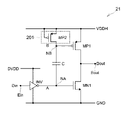
- FIG. 2 is a circuit diagram showing an example of the configuration of the first level shift circuit 21 in the first embodiment.
- the first level shift circuit 21 converts an input signal Din having a voltage level from the reference voltage DVDD to the ground GND into an output signal Dout having a voltage level from the reference voltage VDDH to the ground GND.
- the first level shift circuit 21 level-shifts the high voltage level of the input signal Din from the reference voltage DVDD to the reference voltage VDDH.
- the low voltage levels of input signal Din and output signal Dout are common at ground GND.
- the first level shift circuit 21 includes transistors MN1 and MP1, a capacitor C, a signal input section Ein, a signal output section Eout, a logic inverting element INV, and an impedance section 201.
- the two transistors MN1 and MP1 are cascode-connected between the reference voltage VDDH and the ground GND. Also, the two transistors MN1 and MP1 have different conductivity types.
- the transistor MN1 is arranged on the ground GND side.
- the transistor MN1 is, for example, an N-type MOS (Metal Oxide Semiconductor) transistor.
- Transistor MP1 is arranged on the reference voltage VDDH side.
- Transistor MP1 is, for example, a P-type MOS transistor.
- a capacitor C is connected between the gate of the transistor MN1 and the gate of the transistor MP1.
- An input signal Din having a high or low voltage level is input to the signal input section Ein.
- the signal input section Ein supplies an input signal Din through a capacitor C to at least one of the two gates of the two transistors MN1 and MP1. If the input signal Din is a PWM (Pulse Width Modulation) modulated audio signal, the voltage level of the input signal Din alternately becomes high or low at each modulation time.
- PWM Pulse Width Modulation
- the signal output unit Eout is connected between two cascode-connected transistors MN1 and MP1, and outputs an output signal Dout.
- the logic inverting element INV inverts the logic of the inputted input signal Din and outputs it.
- the logic inverting element INV supplies an input signal Din whose voltage level is inverted between high and low to each of the two gates of the transistors MN1 and MP1.
- the logic inverting element INV is connected between the signal input Ein, the capacitor C and the gate of the transistor MN1.
- a logic inverting element INV (signal input section Ein) is connected to the gate of the transistor MP1 with a capacitor C interposed therebetween.
- the logic inverting element INV (signal input section Ein) is connected to the gate of the transistor MN1 without the capacitor C interposed therebetween.
- the impedance section 201 is an impedance element. More specifically, the impedance section 201 is a high impedance element having an impedance equal to or higher than a predetermined value.
- the impedance section 201 is connected between the gate of the transistor MP1, the capacitor C, and the reference voltage VDDH. Impedance unit 201 biases the voltage level of the gate of transistor MP1 based on reference voltage VDDH. More specifically, impedance section 201 biases (clamps) the voltage level of the gate of transistor MP1 to a predetermined voltage level.
- the impedance unit 201 is, for example, an off transistor (diode-connected transistor) whose gate and source are connected.
- the impedance unit 201 is a transistor MP2 whose gate is connected to the reference voltage VDDH. Transistor MP2 is, for example, a P-type MOS transistor.
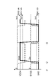
- FIG. 3 is a timing chart showing an example of the operation of the first level shift circuit 21 in the first embodiment.
- the voltage level of input signal Din is low and ground GND.
- the voltage level of the node NA (A in FIG. 3) is the high level obtained by inverting the voltage level of the input signal Din by the logic inverting element INV, and is the reference voltage DVDD.
- the voltage level of node NB (B in FIG. 3) is high, as is the voltage level of node NA.
- the voltage level of the node NB is the voltage level Vp2 higher than the reference voltage VDDH by the threshold voltage Vth of the transistor MP2. This is because the voltage level of node NB is clamped by transistor MP2, as will be described later.
- the voltage level of the node NA is higher than the voltage level Vn1 which is higher than the ground GND by the threshold voltage Vth of the transistor MN1. Therefore, transistor MN1 is on. Also, the voltage level of the node NB is higher than the voltage level Vp1 which is lower than the reference voltage VDDH by the threshold voltage Vth of the transistor MP1. Therefore, transistor MP1 is off. This causes the voltage level of the output signal Dout to be low and ground GND.
- the voltage level of the input signal Din changes from low to high and reaches the reference voltage DVDD.
- the voltage level of the node NA becomes low by inverting the voltage level of the input signal Din by the logic inverting element INV, and becomes the ground GND. Due to capacitive coupling, the voltage level of node NB lowers as the voltage level of node NA lowers. Therefore, the voltage level of node NB becomes low.
- the transistor MN1 When the voltage level of the node NA becomes lower than the voltage level Vn1, the transistor MN1 is turned off. When the voltage level of node NB becomes lower than voltage level Vp1, transistor MP1 is turned on. As a result, the voltage level of the output signal Dout changes from low to high to reach the reference voltage VDDH.
- the impedance unit 201 biases the voltage level of the gate based on the voltage level of the reference voltage VDDH of the transistor MP1 having the gate to which the input signal Din is supplied via the capacitor C. That is, when the voltage level of input signal Din is low, the high voltage level of node NB (gate voltage of transistor MP1) is constrained (clamped) to voltage level Vp2 by transistor MP2. This makes the voltage level of the node NB lower than the voltage level Vp1 by going low. That is, the transistor MP1 can be turned on. As a result, the voltage level of the output signal Dout can be made high at time t2.
- the voltage level of the input signal Din changes from high to low to ground GND.
- the voltage level of the node NA becomes high by inverting the voltage level of the input signal Din by the logic inverting element INV, and becomes the reference voltage DVDD. Due to capacitive coupling, the voltage level of node NB rises as the voltage level of node NA rises. Therefore, the voltage level at node NB goes high and is clamped to voltage level Vp2 as described above. Therefore, as at time t1, the voltage level of the output signal Dout goes low and goes to ground GND.
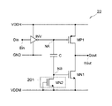
- FIG. 4 is a circuit diagram showing an example of the configuration of the second level shift circuit 22 in the first embodiment.
- the second level shift circuit 22 converts the input signal Din with a voltage level from the reference voltage VDDH to the ground GND into an output signal Dout with a voltage level from the reference voltage VDDH to the reference voltage VDDM.
- the first level shift circuit 21 level-shifts the low voltage level of the input signal Din from the ground GND to the reference voltage VDDM.
- the high voltage level of the input signal Din and the output signal Dout is common at the reference voltage VDDH.
- the logic inverting element INV is connected between the signal input section Ein, the capacitor C and the gate of the transistor MP1.
- a logic inverting element INV (signal input section Ein) is connected to the gate of the transistor MN1 with a capacitor C interposed therebetween.
- the logic inverting element INV (signal input section Ein) is connected to the gate of the transistor MP1 without the capacitor C interposed therebetween.
- the impedance section 201 is connected between the gate of the transistor MN1, the capacitor C, and the reference voltage VDDM. Impedance unit 201 biases the voltage level of the gate of transistor MN1 based on reference voltage VDDM. More specifically, impedance section 201 biases (clamps) the voltage level of the gate of transistor MN1 to a predetermined voltage level.
- the impedance unit 201 is, for example, an off transistor having a gate and a source connected to each other.
- Impedance unit 201 is transistor MN2 whose gate is connected to reference voltage VDDM.
- the transistor MN2 is, for example, an N-type MOS transistor.
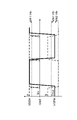
- FIG. 5 is a timing chart showing an example of the operation of the second level shift circuit 22 in the first embodiment.
- the operation of the second level shift circuit 22 is substantially the same as the operation of the first level shift circuit 21 described with reference to FIG.
- the low voltage level of node NB (B in FIG. 5) is clamped to a voltage level lower than reference voltage VDDM by the threshold voltage Vth of transistor MN2. As a result, the voltage level of the node NB becomes high, so that the transistor MN1 can be turned on.
- the transistor MP1 or the transistor MN1 is driven via the capacitor C.
- the impedance unit 201 biases the gate voltage of the transistor MP1 or the transistor MP2 driven through the capacitor C. FIG. As a result, the voltage level can be converted almost without passing through current. As a result, power consumption can be suppressed.
- FIG. 6 is a circuit diagram showing an example of the configuration of the first level shift circuit 21 in the comparative example.
- the first level shift circuit 21 in the comparative example has a cross-couple configuration.
- the first level shift circuit 21 includes two cross-coupled P-type MOS transistors (transistors MPa, MPb) and two N-type MOS transistors (transistors MNa, MNb).
- An input signal Din that has passed through two logic inverting elements INV1 and INV2 is input to the gate of the transistor MNa.
- An input signal Din that has passed through one logic inverting element INV1 is input to the gate of the transistor MNb.
- FIG. 7 is a timing chart showing an example of the operation of the first level shift circuit 21 in the comparative example.
- the voltage level of input signal Din is low.
- the voltage level at the gate of transistor MNa (FIG. 7A) is low and the voltage level at the gate of transistor MNb (FIG. 7B) is high. Therefore, the transistors MNb and MPa are on, and the transistors MNa and MPb are off.
- the voltage level of output signal Dout is low.
- the voltage level of input signal Din changes from low to high.
- the voltage level at the gate of transistor MNa goes from low to high, and the voltage level at the gate of transistor MNb (B in FIG. 7) goes from high to low.
- a current Ia flows through the transistors MPa and MNa that are on.
- the transistor MPa is turned off and the transistor MPb is turned on. This causes the voltage level of the output signal Dout to change from low to high.
- a through current flows at the timing when the voltage level of the input signal Din changes to high or low (logic). This through current increases the power consumption of the level shift circuit.
- the gate voltage of transistor MP1 or transistor MN1 is driven by capacitive coupling without using the cross-couple configuration.
- the number of transistors is three as shown in FIG. 2 or 4, and the number of transistors can be reduced compared to the cross-couple configuration shown in FIG.
- Patent Document 1 As a method for reducing the through current, for example, as in Patent Document 1, a method of using a current source in the cross-couple part and limiting the through current by the current source has been proposed. However, with this method, it is impossible to completely eliminate the feed-through current component, and the operating frequency is slowed down by limiting the current.
- the through current can be made almost zero by the capacitor C. Moreover, since current limitation is not performed, the level shift circuit can be operated at higher speed.
- the effect of reducing power consumption by suppressing through current increases as the number of level shift signals (the number of level shift circuits) increases.
- the number of level shift circuits the number of level shift circuits
- 192 level shift circuits corresponding to 192 bits are used.
- transistors MN1, MP1, MN2, and MP2 are MOS transistors, they are not limited to this, and may be bipolar transistors.
- the impedance section 201 is not limited to a transistor, and may be another impedance element.
- FIG. 8 is a circuit diagram showing an example of the configuration of the first level shift circuit 21 in the second embodiment.
- 2nd Embodiment differs in the structure of the impedance part 201 compared with 1st Embodiment.
- the impedance section 201 is, for example, a reverse diode.
- Impedance section 201 is diode D1.
- the anode of the diode D1 is electrically connected to the low voltage side (ground GND side), and the cathode of the diode D1 is electrically connected to the high voltage side (reference voltage VDDH side).
- Diode D1 functions in much the same way as transistor MP2 of FIG. 2 described in the first embodiment. That is, diode D1 clamps the voltage level of the gate of transistor MP1 based on reference voltage VDDH.
- FIG. 9 is a circuit diagram showing an example of the configuration of the second level shift circuit 22 in the second embodiment.
- the impedance section 201 is a diode D2.
- the anode of diode D2 is arranged on the low voltage side and electrically connected to reference voltage VDDM.
- the cathode of the diode D2 is arranged on the high voltage side and electrically connected to the reference voltage VDDH.
- Diode D2 functions in much the same way as transistor MN2 of FIG. 4 described in the first embodiment. That is, diode D2 clamps the voltage level of the gate of transistor MN1 based on reference voltage VDDM.
- FIG. 10 is a circuit diagram showing an example of the configuration of the first level shift circuit 21 according to the third embodiment. 3rd Embodiment differs in the structure of the impedance part 201 compared with 1st Embodiment.
- the impedance section 201 is, for example, a resistance element R.
- Resistive element R functions together with capacitor C as a high-pass filter.
- the lower limit of the cutoff frequency of the high-pass filter is sufficiently lower than the operating frequency.
- the lower limit of the cut-off frequency of the high-pass filter is preferably, for example, 1/10 of the operating frequency. That is, the resistance value of the resistance element R is set according to the operating frequency of the level shift circuit and the capacitance of the capacitor C, for example, so as to obtain a desired cutoff frequency of the high-pass filter.
- the resistance element R preferably has a resistance value such that the cutoff frequency of the high-pass filter of the resistance element R and the capacitor C is lower than the operating frequency of the level shift circuit.
- a change in voltage is usually converted into a current by a capacitor, and this current is converted into a voltage by flowing through a resistive element.
- the voltage level at the gate of transistor MP1 is biased by the voltage level of reference voltage VDDH and the voltage of resistive element R.
- the resistance element R which is the impedance section 201, can bias the voltage level of the gate of the transistor MP1.
- the resistance value of the resistance element R is set, for example, according to the operating frequency of the level shift circuit and the capacitance of the capacitor C so that a desired voltage of the resistance element R can be obtained.
- the impedance section 201 of the second level shift circuit 22 may also be the resistance element R.
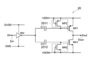
- FIG. 11 is a circuit diagram showing an example of the configuration of the level shift circuit 20 according to the fourth embodiment. Compared to the first embodiment, the fourth embodiment simultaneously converts the voltage level of the first level shift circuit 21 and the voltage level of the second level shift circuit 22 .
- the level shift circuit 20 converts the input signal Din at the voltage level from the reference voltage DVDD to the ground GND into the output signal Dout at the voltage level from the reference voltage VDDH to the reference voltage VDDM.
- the first level shift circuit 21 level-shifts the high voltage level of the input signal Din from the reference voltage DVDD to the reference voltage VDDH, and shifts the low voltage level of the input signal Din from the ground GND to the reference voltage VDDM.
- the high or low voltage level of the input signal Din is different from the voltage levels of the reference voltages VDDH and VDDM.
- one of the high voltage level and the low voltage level of the input signal Din is common to one of the high voltage side and the low voltage side of the voltage level of the output signal Dout.
- the two voltage levels of the output signal Dout are different from the two voltage levels of the input signal Din.
- the level shift circuit 20 includes capacitors C1 and C2 and impedance units 2011 and 2012.
- Capacitors C1 and C2 are connected in series between the gate of transistor MP1 and the gate of transistor MN1. Capacitors C1 and C2 are arranged corresponding to the two transistors MP1 and MN1, respectively.
- the capacitor C1 is connected between the signal input section Ein, the transistor MP1 and the impedance section 2011. Therefore, the logic inverting element INV (signal input section Ein) is connected to the gate of the transistor MP1 via the capacitor C1.
- Capacitor C1 corresponds to capacitor C described with reference to FIG. 2 of the first embodiment.
- Capacitor C2 corresponds to capacitor C described with reference to FIG. 4 of the first embodiment.
- Impedance units 2011 and 2012 bias the voltage levels of the respective gates of the two transistors MP1 and MN1.
- the impedance section 2011 is connected between the capacitor C1 and the transistor MP1 and the reference voltage VDDH. Impedance section 2011 biases the gate of transistor MP1 to a predetermined voltage level.
- the impedance section 2011 corresponds to the impedance section 201 described with reference to FIG. 2 of the first embodiment.
- the impedance section 2012 is connected between the capacitor C2 and the transistor MN1 and the reference voltage VDDM. Impedance section 2012 biases the gate of transistor MN1 to a predetermined voltage level.
- the impedance section 2012 corresponds to the impedance section 201 described with reference to FIG. 4 of the first embodiment.
- the capacitors C1 and C2 and the impedance units 2011 and 2012 may be provided on both the transistor MP1 side and the transistor MN1 side.
- the voltage levels on both the high voltage side and the low voltage side can be level-shifted.
- audio signals often change in voltage level between a positive voltage and a negative voltage with the ground GND interposed therebetween. Therefore, in the audio signal level shift circuit, level shift is performed in a range between a positive voltage (reference voltage VDDH) and a negative voltage (reference voltage VDDM).
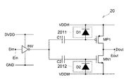
- FIG. 12 is a circuit diagram showing an example of the configuration of the level shift circuit 20 according to the fifth embodiment.
- the fifth embodiment differs from the fourth embodiment in the configurations of impedance units 2011 and 2012 .
- the impedance units 2011 and 2012 are diodes D1 and D2, respectively. Therefore, the fifth embodiment is a combination of the second and fourth embodiments.
- FIG. 13 is a circuit diagram showing an example of the configuration of the first level shift circuit 21 according to the sixth embodiment.
- the first level shift circuit 21 further includes a HiZ (high impedance) detection circuit 202 and a logic fixing circuit 203 .
- a HiZ detection circuit 202 as a high impedance detection section detects that the signal output section Eout is high impedance.
- a logic fixing circuit 203 as a logic fixing section fixes the logic of the signal output section Eout. That is, the logic fixing circuit 203 fixes the voltage level of the output signal Dout to one of the two reference voltages when the signal output section Eout is in high impedance.
- the voltage level of the input signal Din is fixed (left) high, the voltage level of the node NB is fixed low. In this case, a leakage current may flow from the reference voltage VDDH through the transistor MP2 to the node NB, and the voltage level of the node NB may rise.
- transistor MP1 when the voltage level of node NB exceeds voltage level Vp1, transistor MP1 is turned off. Therefore, both the transistors MP1 and MN1 are turned off, and the signal output section Eout becomes high impedance (floating state). When the signal output section Eout becomes high impedance, a through current may flow in the output destination circuit of the first level shift circuit 21 .
- the HiZ detection circuit 202 detects that the signal output section Eout is in high impedance, and the logic fixing circuit 203 fixes the logic of the output to the voltage level of the reference voltage VDDH. As a result, it is possible to suppress the output from becoming high impedance, and to suppress the through current from flowing in the circuit of the output destination.
- the second level shift circuit 22 shown in FIG. 4 of the first embodiment may also be provided with the HiZ detection circuit 202 and the logic fixation circuit 203 . If the voltage level of input signal Din is fixed (left) low, the voltage level of node NB is fixed high. In this case, a leakage current may flow from the node NB through the transistor MN2 to the reference voltage VDDM, and the voltage level of the node NB may drop. In this case, since the transistor MN1 is turned off from the on state, the signal output section Eout becomes high impedance. Therefore, the logic fixing circuit 203 fixes the output logic to the voltage level of the reference voltage VDDM. As a result, it is possible to prevent the output from becoming high impedance in the second level shift circuit 22 as well, and it is possible to prevent a through current from flowing in the output destination circuit.
- FIG. 14 is a circuit diagram showing an example of the configuration of the first level shift circuit 21 according to the seventh embodiment.
- the seventh embodiment differs from the sixth embodiment in that the HiZ detection circuit 202 acquires the signal of the node NA.
- a HiZ detection circuit 202 as a level detection unit detects the voltage level of the gate (node NA) of the transistor MN1.
- the logic fixing circuit 203 fixes the voltage level of the output signal Dout to one of the two reference voltages when the voltage level of the gate of the transistor MN1 is low for a predetermined period or longer.
- the input signal Din is fixed at high and the voltage levels of the gates of the transistors MN1 and MP1 are fixed at low, whereby the signal output section Eout becomes high impedance. Therefore, the voltage level of the gate of transistor MN1 may be used to determine the logic fixation of logic fixation circuit 203.
- FIG. 1 the input signal Din is fixed at high and the voltage levels of the gates of the transistors MN1 and MP1 are fixed at low, whereby the signal output section Eout becomes high impedance. Therefore, the voltage level of the gate of transistor MN1 may be used to determine the logic fixation of logic fixation circuit 203.
- the logic fixing determination is not limited to the voltage level of the gate of the transistor MN1.
- the HiZ detection circuit 202 may detect, for example, the input signal Din or the voltage level of the gate (node NB) of the transistor MP1.
- the logic fixing circuit 203 may fix the logic of the signal output section Eout based on, for example, the input signal Din or the voltage level of the gate of the transistor MP1.
- this technique can take the following structures. (1) two transistors of different conductivity types cascode-connected between two reference voltages having different voltage levels; a signal input unit that supplies an input signal having a high-level or low-level voltage level through a capacitor to at least one of two control terminals of the two transistors, respectively; and an impedance unit that biases the voltage level of the control terminal to which the input signal is supplied via the capacitor to a predetermined voltage level.
- the impedance section includes the reference voltage of the transistor having the control terminal to which the input signal is supplied via the capacitor, and the control terminal to which the input signal is supplied via the capacitor;
- the two transistors are a first transistor on the first reference voltage side; a second transistor on a second reference voltage side having a voltage level different from the first reference voltage;
- the signal input section supplies the input signal to a first control terminal of the first transistor through the capacitor and supplies the input signal to a second control terminal of the second transistor without the capacitor.
- the level shift circuit according to any one of (1) to (4), wherein the impedance section biases the voltage level of the first control terminal to a predetermined voltage level.
- the two transistors a first transistor on the first reference voltage side; a second transistor on a second reference voltage side having a voltage level different from the first reference voltage;
- the signal input section supplies the input signal to a first control terminal of the first transistor via a first capacitor, and the second control terminal of the second transistor via a second capacitor different from the first capacitor.
- the impedance section is a first impedance unit that biases the voltage level of the first control terminal to a predetermined voltage level;
- a signal output unit connected between the two cascode-connected transistors for outputting an output signal obtained by converting the voltage level of the input signal; a high impedance detection unit that detects that the signal output unit is high impedance; (1) to (9), further comprising a logic fixing unit that fixes the voltage level of the output signal to one of the two reference voltages when the signal output unit is high impedance.
- a signal output unit connected between the two cascode-connected transistors for outputting an output signal obtained by converting the voltage level of the input signal; a level detection unit that detects the voltage level of at least one of the input signal and the two control terminals; When the voltage level of the input signal and at least one of the two control terminals continues at a high level or a low level for a predetermined period or longer, the voltage level of the output signal is set to either one of the two reference voltages.
- the level shift circuit according to any one of (1) to (9), further comprising a logic fixer that fixes the level.
- the impedance unit is a diode; the anode of the diode is electrically connected to the lower voltage side of the two reference voltages; The level shift circuit according to any one of (1) to (11), wherein the cathode of the diode is electrically connected to a higher voltage side of the two reference voltages.
- the impedance unit is a resistive element, The level shift circuit according to any one of (1) to (11), wherein the resistance element has a resistance value corresponding to the operating frequency of the level shift circuit and the capacitance of the capacitor.
- the level shift circuit according to any one of (1) to (16) wherein the voltage level of the input signal alternates between high level and low level depending on time.
- a DAC Digital to Analog Converter
- the level shift circuit is two transistors of different conductivity types cascoded between two reference voltages having different voltage levels; a signal input unit that supplies an input signal having a high-level or low-level voltage level through a capacitor to at least one of two control terminals of the two transistors, respectively; and an impedance section that biases the voltage level of the control terminal to which the input signal is supplied via the capacitor to a predetermined voltage level.
Landscapes
- Engineering & Computer Science (AREA)
- Computer Hardware Design (AREA)
- Physics & Mathematics (AREA)
- Computing Systems (AREA)
- General Engineering & Computer Science (AREA)
- Mathematical Physics (AREA)
- Logic Circuits (AREA)
Priority Applications (1)
| Application Number | Priority Date | Filing Date | Title |
|---|---|---|---|
| JP2023505201A JPWO2022190702A1 (cg-RX-API-DMAC7.html) | 2021-03-08 | 2022-01-31 |
Applications Claiming Priority (2)
| Application Number | Priority Date | Filing Date | Title |
|---|---|---|---|
| JP2021036491 | 2021-03-08 | ||
| JP2021-036491 | 2021-03-08 |
Publications (1)
| Publication Number | Publication Date |
|---|---|
| WO2022190702A1 true WO2022190702A1 (ja) | 2022-09-15 |
Family
ID=83226635
Family Applications (1)
| Application Number | Title | Priority Date | Filing Date |
|---|---|---|---|
| PCT/JP2022/003479 Ceased WO2022190702A1 (ja) | 2021-03-08 | 2022-01-31 | レベルシフト回路及び電子機器 |
Country Status (2)
| Country | Link |
|---|---|
| JP (1) | JPWO2022190702A1 (cg-RX-API-DMAC7.html) |
| WO (1) | WO2022190702A1 (cg-RX-API-DMAC7.html) |
Citations (5)
| Publication number | Priority date | Publication date | Assignee | Title |
|---|---|---|---|---|
| JPS55491A (en) * | 1979-05-04 | 1980-01-05 | Citizen Watch Co Ltd | Electronic watch |
| JPS6444619A (en) * | 1987-08-12 | 1989-02-17 | Seiko Epson Corp | Level shift circuit |
| JPH09172367A (ja) * | 1995-12-20 | 1997-06-30 | Seiko Epson Corp | レベルシフタ回路 |
| JP2003110420A (ja) * | 2001-06-26 | 2003-04-11 | Seiko Epson Corp | レベルシフタ及びそれを用いた電気光学装置 |
| JP2009188734A (ja) * | 2008-02-06 | 2009-08-20 | Nec Electronics Corp | レベルシフト回路及びそれを用いたドライバと表示装置 |
Family Cites Families (3)
| Publication number | Priority date | Publication date | Assignee | Title |
|---|---|---|---|---|
| KR100218506B1 (ko) * | 1996-12-14 | 1999-09-01 | 윤종용 | 액정 표시 장치용 레벨 시프트 회로 |
| JPH1168534A (ja) * | 1997-08-25 | 1999-03-09 | Sony Corp | 高電圧駆動回路 |
| JP2009130879A (ja) * | 2007-11-28 | 2009-06-11 | Ricoh Co Ltd | レベルシフト回路 |
-
2022
- 2022-01-31 JP JP2023505201A patent/JPWO2022190702A1/ja active Pending
- 2022-01-31 WO PCT/JP2022/003479 patent/WO2022190702A1/ja not_active Ceased
Patent Citations (5)
| Publication number | Priority date | Publication date | Assignee | Title |
|---|---|---|---|---|
| JPS55491A (en) * | 1979-05-04 | 1980-01-05 | Citizen Watch Co Ltd | Electronic watch |
| JPS6444619A (en) * | 1987-08-12 | 1989-02-17 | Seiko Epson Corp | Level shift circuit |
| JPH09172367A (ja) * | 1995-12-20 | 1997-06-30 | Seiko Epson Corp | レベルシフタ回路 |
| JP2003110420A (ja) * | 2001-06-26 | 2003-04-11 | Seiko Epson Corp | レベルシフタ及びそれを用いた電気光学装置 |
| JP2009188734A (ja) * | 2008-02-06 | 2009-08-20 | Nec Electronics Corp | レベルシフト回路及びそれを用いたドライバと表示装置 |
Also Published As
| Publication number | Publication date |
|---|---|
| JPWO2022190702A1 (cg-RX-API-DMAC7.html) | 2022-09-15 |
Similar Documents
| Publication | Publication Date | Title |
|---|---|---|
| US7675363B2 (en) | Differential amplifier circuit and A/D converter | |
| JP5431992B2 (ja) | トランスミッションゲート及び半導体装置 | |
| KR100791934B1 (ko) | 고속 신호 전송 시스템의 고전압 출력 버퍼 회로 | |
| CN106899288B (zh) | 电平转换电路 | |
| US6388477B1 (en) | Switchable voltage follower and bridge driver using the same | |
| WO2021111772A1 (ja) | 比較回路、半導体装置 | |
| JP4928290B2 (ja) | 差動信号比較器 | |
| CN109417606B (zh) | 一种可输出正负电压的电平转换器 | |
| JP2017175368A (ja) | レベルシフト回路 | |
| JP4481314B2 (ja) | 信号変換回路 | |
| US7400171B1 (en) | Electronic switch having extended voltage range | |
| US20120176263A1 (en) | Current switch circuit and da converter | |
| JP4537840B2 (ja) | 電流源セルおよびそれを用いたd/aコンバータ | |
| KR100453424B1 (ko) | 반도체 집적 회로 | |
| JP5483424B2 (ja) | レベル変換回路 | |
| US8963582B2 (en) | Signal amplification circuit and method | |
| JP4443889B2 (ja) | 差動増幅器 | |
| TWI789242B (zh) | 電位轉換電路 | |
| US9000964B2 (en) | Circuit and method for signal conversion | |
| CN114204935B (zh) | 缓冲电路 | |
| JP4939291B2 (ja) | 半導体回路 | |
| JP2010098563A (ja) | コンパレータ | |
| JP2010206458A (ja) | レシーバ回路 | |
| JP3667616B2 (ja) | レベル変換回路 | |
| CN106656179A (zh) | 一种电压限幅电路 |
Legal Events
| Date | Code | Title | Description |
|---|---|---|---|
| 121 | Ep: the epo has been informed by wipo that ep was designated in this application |
Ref document number: 22766669 Country of ref document: EP Kind code of ref document: A1 |
|
| ENP | Entry into the national phase |
Ref document number: 2023505201 Country of ref document: JP Kind code of ref document: A |
|
| NENP | Non-entry into the national phase |
Ref country code: DE |
|
| 122 | Ep: pct application non-entry in european phase |
Ref document number: 22766669 Country of ref document: EP Kind code of ref document: A1 |