WO2022190243A1 - めっき装置、およびめっき方法 - Google Patents
めっき装置、およびめっき方法 Download PDFInfo
- Publication number
- WO2022190243A1 WO2022190243A1 PCT/JP2021/009476 JP2021009476W WO2022190243A1 WO 2022190243 A1 WO2022190243 A1 WO 2022190243A1 JP 2021009476 W JP2021009476 W JP 2021009476W WO 2022190243 A1 WO2022190243 A1 WO 2022190243A1
- Authority
- WO
- WIPO (PCT)
- Prior art keywords
- plating
- substrate
- paddle
- resistor
- anode
- Prior art date
- Legal status (The legal status is an assumption and is not a legal conclusion. Google has not performed a legal analysis and makes no representation as to the accuracy of the status listed.)
- Ceased
Links
Images








Classifications
-
- C—CHEMISTRY; METALLURGY
- C25—ELECTROLYTIC OR ELECTROPHORETIC PROCESSES; APPARATUS THEREFOR
- C25D—PROCESSES FOR THE ELECTROLYTIC OR ELECTROPHORETIC PRODUCTION OF COATINGS; ELECTROFORMING; APPARATUS THEREFOR
- C25D17/00—Constructional parts, or assemblies thereof, of cells for electrolytic coating
- C25D17/02—Tanks; Installations therefor
-
- C—CHEMISTRY; METALLURGY
- C25—ELECTROLYTIC OR ELECTROPHORETIC PROCESSES; APPARATUS THEREFOR
- C25D—PROCESSES FOR THE ELECTROLYTIC OR ELECTROPHORETIC PRODUCTION OF COATINGS; ELECTROFORMING; APPARATUS THEREFOR
- C25D17/00—Constructional parts, or assemblies thereof, of cells for electrolytic coating
- C25D17/001—Apparatus specially adapted for electrolytic coating of wafers, e.g. semiconductors or solar cells
-
- C—CHEMISTRY; METALLURGY
- C25—ELECTROLYTIC OR ELECTROPHORETIC PROCESSES; APPARATUS THEREFOR
- C25D—PROCESSES FOR THE ELECTROLYTIC OR ELECTROPHORETIC PRODUCTION OF COATINGS; ELECTROFORMING; APPARATUS THEREFOR
- C25D17/00—Constructional parts, or assemblies thereof, of cells for electrolytic coating
- C25D17/002—Cell separation, e.g. membranes, diaphragms
-
- C—CHEMISTRY; METALLURGY
- C25—ELECTROLYTIC OR ELECTROPHORETIC PROCESSES; APPARATUS THEREFOR
- C25D—PROCESSES FOR THE ELECTROLYTIC OR ELECTROPHORETIC PRODUCTION OF COATINGS; ELECTROFORMING; APPARATUS THEREFOR
- C25D17/00—Constructional parts, or assemblies thereof, of cells for electrolytic coating
- C25D17/008—Current shielding devices
-
- C—CHEMISTRY; METALLURGY
- C25—ELECTROLYTIC OR ELECTROPHORETIC PROCESSES; APPARATUS THEREFOR
- C25D—PROCESSES FOR THE ELECTROLYTIC OR ELECTROPHORETIC PRODUCTION OF COATINGS; ELECTROFORMING; APPARATUS THEREFOR
- C25D17/00—Constructional parts, or assemblies thereof, of cells for electrolytic coating
- C25D17/06—Suspending or supporting devices for articles to be coated
-
- C—CHEMISTRY; METALLURGY
- C25—ELECTROLYTIC OR ELECTROPHORETIC PROCESSES; APPARATUS THEREFOR
- C25D—PROCESSES FOR THE ELECTROLYTIC OR ELECTROPHORETIC PRODUCTION OF COATINGS; ELECTROFORMING; APPARATUS THEREFOR
- C25D21/00—Processes for servicing or operating cells for electrolytic coating
- C25D21/10—Agitating of electrolytes; Moving of racks
-
- C—CHEMISTRY; METALLURGY
- C25—ELECTROLYTIC OR ELECTROPHORETIC PROCESSES; APPARATUS THEREFOR
- C25D—PROCESSES FOR THE ELECTROLYTIC OR ELECTROPHORETIC PRODUCTION OF COATINGS; ELECTROFORMING; APPARATUS THEREFOR
- C25D21/00—Processes for servicing or operating cells for electrolytic coating
- C25D21/12—Process control or regulation
-
- C—CHEMISTRY; METALLURGY
- C25—ELECTROLYTIC OR ELECTROPHORETIC PROCESSES; APPARATUS THEREFOR
- C25D—PROCESSES FOR THE ELECTROLYTIC OR ELECTROPHORETIC PRODUCTION OF COATINGS; ELECTROFORMING; APPARATUS THEREFOR
- C25D5/00—Electroplating characterised by the process; Pretreatment or after-treatment of workpieces
- C25D5/02—Electroplating of selected surface areas
- C25D5/022—Electroplating of selected surface areas using masking means
Definitions
- This application relates to plating equipment and plating methods.
- a cup-type electroplating device is known as an example of a plating device.
- a cup-type electroplating apparatus immerses a substrate (for example, a semiconductor wafer) held in a substrate holder with the surface to be plated facing downward in a plating solution, and applies a voltage between the substrate and the anode to A conductive film is deposited on the surface of the substrate.
- Patent Document 1 discloses disposing a ring-shaped shield with an opening in the center between a substrate and an anode in a cup-type electrolytic plating apparatus. Further, Patent Document 1 discloses that the thickness of the plated film formed on the substrate is made uniform by adjusting the size of the opening of the shield and adjusting the distance between the shield and the substrate. It is
- the conventional technology has room for improvement in improving the uniformity of the plating film thickness formed on the substrate.
- the conventional technology makes the thickness of the plating formed on the substrate uniform by adjusting the size of the shield opening and adjusting the distance between the shield and the substrate.
- one object of the present application is to improve the uniformity of the plating film thickness formed on the substrate.
- a plating bath for containing a plating solution, a substrate holder for holding a substrate, an anode housed in the plating bath, a substrate held by the substrate holder and the anode and an anode mask having an opening formed in the center; and a plurality of holes spaced apart from the anode mask between the substrate held by the substrate holder and the anode mask.
- a plating apparatus is disclosed, including a formed resistor.
- FIG. 1 is a perspective view showing the overall configuration of the plating apparatus of this embodiment.
- FIG. 2 is a plan view showing the overall configuration of the plating apparatus of this embodiment.
- FIG. 3 is a longitudinal sectional view schematically showing the configuration of the plating module of one embodiment.
- FIG. 4 is a diagram schematically showing measurement of plating film thickness distribution by a sensor.
- FIG. 5 is a plan view schematically showing an anode mask.
- FIG. 6 is a diagram schematically showing plating film thickness distribution when the diameter of the opening of the anode mask is changed.
- FIG. 7 is a diagram schematically showing plating film thickness distribution when the distance between the substrate and the resistor is changed.
- FIG. 1 is a perspective view showing the overall configuration of the plating apparatus of this embodiment.
- FIG. 2 is a plan view showing the overall configuration of the plating apparatus of this embodiment.
- FIG. 3 is a longitudinal sectional view schematically showing the configuration of the plating module of one embodiment.
- FIG. 4 is
- FIG. 8 is a diagram schematically showing the plating film thickness distribution at the outer edge of the substrate when the distance between the substrate and the resistor is changed.
- FIG. 9 is a longitudinal sectional view schematically showing the configuration of the plating module of one embodiment.
- FIG. 10 is a diagram showing the flow velocity of the plating solution on the surface to be plated when the distance between the substrate and the resistor is changed.
- FIG. 11 is a longitudinal sectional view schematically showing the configuration of the plating module of one embodiment.
- FIG. 12 is a longitudinal sectional view schematically showing the configuration of the plating module of one embodiment.
- FIG. 13 is a diagram showing the flow velocity of the plating solution on the surface to be plated when the distance between the substrate and the resistor is changed.
- FIG. 14 is a flow chart showing the plating method of this embodiment.
- FIG. 1 is a perspective view showing the overall configuration of the plating apparatus of this embodiment.
- FIG. 2 is a plan view showing the overall configuration of the plating apparatus of this embodiment.
- the plating apparatus 1000 includes a load port 100, a transfer robot 110, an aligner 120, a pre-wet module 200, a pre-soak module 300, a plating module 400, a cleaning module 500, a spin rinse dryer 600, and a transfer device. 700 and a control module 800 .
- the load port 100 is a module for loading substrates stored in cassettes such as FOUPs (not shown) into the plating apparatus 1000 and for unloading substrates from the plating apparatus 1000 to cassettes. Although four load ports 100 are arranged horizontally in this embodiment, the number and arrangement of the load ports 100 are arbitrary.
- the transport robot 110 is a robot for transporting substrates, and is configured to transfer substrates among the load port 100 , the aligner 120 and the transport device 700 . When transferring substrates between the transfer robot 110 and the transfer device 700, the transfer robot 110 and the transfer device 700 can transfer the substrates via a temporary placement table (not shown).
- the aligner 120 is a module for aligning the positions of orientation flats, notches, etc. of the substrate in a predetermined direction. Although two aligners 120 are arranged horizontally in this embodiment, the number and arrangement of the aligners 120 are arbitrary.
- the pre-wet module 200 replaces the air inside the pattern formed on the substrate surface with the treatment liquid by wetting the surface to be plated of the substrate before the plating treatment with a treatment liquid such as pure water or degassed water.
- the pre-wet module 200 is configured to perform a pre-wet process that facilitates the supply of the plating solution to the inside of the pattern by replacing the treatment solution inside the pattern with the plating solution during plating. Although two pre-wet modules 200 are arranged vertically in this embodiment, the number and arrangement of the pre-wet modules 200 are arbitrary.
- the presoak module 300 for example, an oxide film having a large electric resistance existing on the surface of a seed layer formed on the surface to be plated of the substrate before plating is etched away with a processing liquid such as sulfuric acid or hydrochloric acid, and the surface of the plating substrate is cleaned.
- a processing liquid such as sulfuric acid or hydrochloric acid
- it is configured to perform a pre-soak process for activation.
- two presoak modules 300 are arranged side by side in the vertical direction, but the number and arrangement of the presoak modules 300 are arbitrary.
- the plating module 400 applies plating to the substrate.
- the cleaning module 500 is configured to perform a cleaning process on the substrate in order to remove the plating solution and the like remaining on the substrate after the plating process.
- the spin rinse dryer 600 is a module for drying the substrate after cleaning by rotating it at high speed. Although two spin rinse dryers are arranged vertically in this embodiment, the number and arrangement of the spin rinse dryers are arbitrary.
- the transport device 700 is a device for transporting substrates between a plurality of modules within the plating apparatus 1000 .
- Control module 800 is configured to control a plurality of modules of plating apparatus 1000 and may comprise, for example, a general purpose or dedicated computer with input/output interfaces to an operator.
- a substrate stored in a cassette is loaded into the load port 100 .
- the transport robot 110 takes out the substrate from the cassette of the load port 100 and transports the substrate to the aligner 120 .
- the aligner 120 aligns orientation flats, notches, etc. of the substrate in a predetermined direction.
- the transport robot 110 transfers the substrate aligned by the aligner 120 to the transport device 700 .
- the transport device 700 transports the substrate received from the transport robot 110 to the pre-wet module 200 .
- the pre-wet module 200 pre-wets the substrate.
- the transport device 700 transports the pre-wet processed substrate to the pre-soak module 300 .
- the presoak module 300 applies a presoak treatment to the substrate.
- the transport device 700 transports the presoaked substrate to the plating module 400 .
- the plating module 400 applies plating to the substrate.
- the transport device 700 transports the plated substrate to the cleaning module 500 .
- the cleaning module 500 performs a cleaning process on the substrate.
- the transport device 700 transports the cleaned substrate to the spin rinse dryer 600 .
- a spin rinse dryer 600 performs a drying process on the substrate.
- the transport device 700 delivers the dried substrate to the transport robot 110 .
- the transport robot 110 transports the substrate received from the transport device 700 to the cassette of the load port 100 . Finally, the cassette containing the substrates is unloaded from the load port 100 .
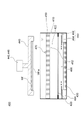
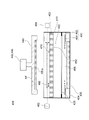
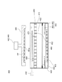
- FIG. 3 is a longitudinal sectional view schematically showing the configuration of the plating module 400 of one embodiment. As shown in FIG.
- plating module 400 includes a plating bath 410 for containing a plating solution.
- the plating module 400 includes a membrane 420 that vertically separates the interior of the plating bath 410 .
- the membrane 420 is composed of, for example, an elastic thin film.
- the interior of the plating tank 410 is partitioned by a membrane 420 into a cathode area 422 in which the substrate Wf is immersed and an anode area 424 in which an anode is arranged. Cathode region 422 and anode region 424 are each filled with a plating solution.
- Plating module 400 includes an anode 430 positioned on the bottom surface of plating bath 410 in anode region 424 .
- the plating module 400 includes a substrate holder 440 for holding the substrate Wf with the surface to be plated Wf-a facing downward.
- the substrate holder 440 includes power contacts for powering the substrate Wf from a power source (not shown).
- the feed contacts are adapted to contact and feed the outer edge of the substrate Wf.
- the plating module 400 includes a distance adjustment mechanism 442 for adjusting the distance between the substrate holder 440 and a resistor 450, which will be described later.
- the distance adjustment mechanism 442 is implemented by a holder elevating mechanism that elevates the substrate holder 440 to adjust the position of the substrate holder 440 with respect to the resistor 450 .
- the distance adjusting mechanism (holder elevating mechanism) 442 can be implemented by a known mechanism such as a motor.
- the plating module 400 immerses the substrate Wf in the plating solution in the cathode region 422 using the distance adjusting mechanism (holder elevating mechanism) 442, and applies a voltage between the anode 430 and the substrate Wf, thereby increasing the thickness of the substrate Wf.
- the plating surface Wf-a is configured to be plated. Note that the distance adjusting mechanism 442 is not limited to a configuration in which the distance between the substrate holder 440 and the resistor 450 is adjusted by raising and lowering the substrate holder 440 by the holder raising and lowering mechanism.
- the distance adjustment mechanism 442 may include a resistor elevating mechanism that elevates the resistor 450 to adjust the position of the resistor 450 with respect to the substrate holder 440 instead of the holder elevating mechanism.
- the distance adjustment mechanism 442 may include both the holder lifting mechanism and the resistor lifting mechanism.
- the plating module 400 includes a rotation mechanism 446 for rotating the substrate holder 440 so that the substrate Wf rotates around a virtual rotation axis extending vertically through the center of the surface to be plated Wf-a.
- the rotating mechanism 446 can be implemented by a known mechanism such as a motor.
- the plating module 400 includes a sensor 470 capable of measuring the plating film thickness distribution or current density distribution along the radial direction of the plating surface Wf-a of the substrate Wf.
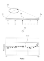
- FIG. 4 is a diagram schematically showing measurement of plating film thickness distribution by a sensor. As shown in FIG. 4, the sensor 470 of one embodiment detects the It is configured to measure plating film thickness or current density. The sensor 470 acquires information such as plating film thickness or current density at a plurality of monitoring points using any method such as optical, electric field, magnetic field, potential, etc. at regular time intervals during the plating process.
- the plating module 400 is configured to acquire the plating film thickness distribution Th-1 in the radial direction of the plating surface Wf-a of the substrate Wf based on the information acquired by the sensor 470 .
- the sensor 470 is arranged on a resistor 450, which will be described later, but the arrangement position of the sensor 470 is arbitrary.
- the plating module 400 includes an anode mask 460 arranged between the substrate Wf held by the substrate holder 440 and the anode 430 .
- Anode mask 460 is positioned adjacent anode 430 in anode region 424 .
- the anode mask 460 is a ring-shaped electric field shield with an opening 466 formed in the center.
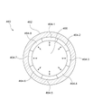
- FIG. 5 is a plan view schematically showing an anode mask.
- the anode mask 460 includes a ring-shaped first anode mask 462 fixed to the inner wall of the plating tank 410 and arranged along the circumferential direction on the first anode mask 462. and a plurality of second anode masks 464 .
- second anode masks 464 comprise eight second anode masks 464-1 through 464-8, although the number of second anode masks 464 is arbitrary.
- Each of the plurality of second anode masks 464 is configured to be movable along the radial direction of the first anode mask 462 .
- the anode mask 460 can reduce the diameter of the openings 466 of the anode mask 460 by moving the plurality of second anode masks 464 radially inward of the first anode mask 462 .
- the anode mask 460 can increase the diameter of the openings 466 of the anode mask 460 by moving the plurality of second anode masks 464 radially outward of the first anode mask 462 .
- Anode mask 460 acts to substantially change the diameter of anode 430 by changing the diameter of opening 466 .
- the anode mask 460 acts to change the overall film thickness distribution from the center to the outer edge of the substrate Wf by changing the diameter of the opening 466 . This point will be described below.
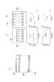
- FIG. 6 is a diagram schematically showing the plating film thickness distribution when the diameter of the opening of the anode mask is changed.
- the vertical axis indicates the plating film thickness
- the horizontal axis indicates the radial position from the central portion Ct to the outer edge portion Eg of the plating surface Wf-a of the substrate Wf.
- plating film thickness distributions Th-11 to Th-17 sequentially show plating film thickness distributions when the diameter of the opening 466 of the anode mask 460 is increased.
- changing the diameter of the opening 466 of the anode mask 460 changes the plating film thickness from the central portion Ct to the outer edge portion Eg of the substrate Wf. Specifically, when the diameter of the opening 466 of the anode mask 460 is small, the electric field concentrates near the central portion Ct of the substrate Wf. The plating film thickness becomes thicker, and the plating film thickness of the outer edge portion Eg of the substrate Wf becomes thinner. On the other hand, when the diameter of the opening 466 of the anode mask 460 is large, the electric field concentrates on the outer edge Eg of the substrate Wf. It becomes thinner, and the plating film thickness of the outer edge portion Eg of the substrate Wf becomes thicker. In the example of FIG. 6, the plating film thickness distribution is most uniform when the plating film thickness distribution is Th-14. It is required to uniformize the thickness of the plating film in the vicinity of the outer edge Eg.
- the plating module 400 of one embodiment includes a resistor element disposed between the substrate Wf held by the substrate holder 440 and the anode mask 460 and spaced apart from the anode mask 460.
- 450 is provided.
- Resistor 450 is disposed in cathode region 422 .
- the resistor 450 is configured by a plate-like member (punching plate) in which a plurality of through holes 452 passing through the anode region 424 and the cathode region 422 are formed.
- the shape of resistor 450 is arbitrary.
- the resistor 450 is not limited to a punching plate, and can be composed of, for example, a porous body in which a large number of pores are formed in a ceramic material.
- the resistor 450 acts as a resistor between the anode 430 and the substrate Wf.
- the resistor 450 has a resistivity of, for example, 1 ⁇ m or more, preferably 3 ⁇ m or more, but is not limited to this and the resistivity of the resistor 450 is arbitrary. By arranging the resistor 450, the resistance value between the anode 430 and the substrate Wf is increased, so that the electric field is less likely to spread. Uniform distribution can be achieved.
- the resistor 450 particularly affects the plating film thickness distribution at the outer edge of the plating surface Wf-a of the substrate Wf. That is, the distance adjustment mechanism 442 is configured to adjust the distance between the substrate holder 440 and the resistor 450 based on the plating film thickness distribution or current density distribution measured by the sensor 470 . Specifically, the distance adjusting mechanism (holder elevating mechanism) 442 is configured to elevate the substrate holder 440 based on the plating film thickness distribution or current density distribution measured by the sensor 470 . By raising and lowering the substrate holder 440, the distance between the substrate Wf and the resistor 450 changes.
- FIG. 7 is a diagram schematically showing the plating film thickness distribution when the distance between the substrate and the resistor is changed.
- the vertical axis indicates the plating film thickness
- the horizontal axis indicates the radial position from the central portion Ct to the outer edge portion Eg of the plating surface Wf-a of the substrate Wf.
- plating film thickness distributions Th-21, Th-22, and Th-23 indicate plating film thickness distributions when the distance between the substrate Wf and the resistor 450 is increased.
- the plating film thickness near the outer edge Eg of the substrate Wf changes greatly. This point will be described below.
- FIG. 8 is a diagram schematically showing the plating film thickness distribution at the outer edge of the substrate when the distance between the substrate and the resistor is changed.
- FIG. 8A shows the plating film thickness distribution when the distance between the substrate Wf and the resistor 450 is shortened
- FIG. It shows the plating film thickness distribution in the case of As shown in FIG. 8, increasing the distance between the substrate Wf and the resistor 450 increases the space in which the electric field can spread. Since the power supply contact of the substrate holder 440 is in contact with the outer edge of the substrate Wf, the electric field relatively concentrates on the outer edge of the substrate Wf, and the plating thickness of the outer edge increases.
- the plating module 400 can adjust the plating film thickness of the outer edge of the substrate Wf by the distance adjustment mechanism 442 .
- the distance adjustment mechanism (holder elevating mechanism) 442 moves between the substrate Wf and the resistor 450.
- the uniform plating film thickness distribution such as the plating film thickness distribution Th-25.
- the distance adjustment mechanism (holder elevating mechanism) 442 moves the substrate Wf and the resistor 450 together.
- the uniform plating film thickness distribution such as the plating film thickness distribution Th-27.
- the plating film thickness distribution is determined by the size of the opening 466 of the anode mask 460, the type of plating solution, the current density on the surface to be plated Wf-a, and the like.
- the plating module 400 of one embodiment includes both the anode mask 460 and the resistor 450. Therefore, the plating module 400 can improve the uniformity of the plating film thickness distribution over the entire substrate Wf by using the respective characteristics of the anode mask 460 and the resistor 450 . For example, while plating the substrate Wf, the plating module 400 uses the sensor 470 to measure the plating film thickness distribution or the current density distribution along the radial direction of the plating surface Wf-a of the substrate Wf. measure.
- the plating module 400 adjusts the size of the diameter of the opening 466 of the anode mask 460 based on the plating film thickness distribution or current density distribution measured by the sensor 470 .
- the plating film thickness between the central portion Ct of the plating surface Wf-a shown in FIG. 6 and the midpoint Md between the central portion Ct and the outer edge portion Eg of the plating surface Wf-a Alternatively, the size of the diameter of the opening 466 of the anode mask 460 is adjusted so that the difference in current density becomes small. This improves the uniformity of the plating film thickness between the central portion Ct and the midpoint Md of the surface to be plated Wf-a of the substrate Wf.
- the plating module 400 adjusts the distance between the substrate Wf and the resistor 450 by raising and lowering the substrate holder 440 based on the plating film thickness distribution or current density distribution measured by the sensor 470 .
- the plating film thickness between the middle point Md between the central portion Ct and the outer edge portion Eg of the surface to be plated Wf-a shown in FIG. 7 and the outer edge portion Eg of the surface to be plated Wf-a Alternatively, the substrate holder 440 is moved up and down so that the difference in current density becomes smaller. This improves the uniformity of the plating film thickness between the middle point Md of the plating surface Wf-a of the substrate Wf and the outer edge Eg.
- the plating module 400 adjusts the diameter of the opening 466 of the anode mask 460 and the distance between the substrate Wf and the resistor 450 while performing the plating process.
- the uniformity of the plating film thickness distribution on the plating surface Wf-a can be improved.
- an example is shown in which the diameter of the opening 466 of the anode mask 460 is adjusted and the distance between the substrate Wf and the resistor 450 is adjusted while performing the plating process, but the present invention is not limited to this. .
- the optimum values for the diameter of the opening 466 of the anode mask 460 and the distance between the substrate Wf and the resistor 450 are obtained in advance. It is not necessary to adjust the diameter of the opening 466 of 460 and the elevation of the substrate holder 440 .
- FIG. 9 is a longitudinal sectional view schematically showing the configuration of the plating module of one embodiment.
- the embodiment of FIG. 9 has a configuration similar to that of the embodiment shown in FIG. 3, except that a paddle, a paddle stirring mechanism, and the like are provided. Therefore, description overlapping with the embodiment shown in FIG. 3 will be omitted.
- the plating module 400 includes a paddle 480 arranged between a substrate Wf held by a substrate holder 440 and a resistor 450, and a paddle stirring mechanism for stirring the paddle 480 in the plating solution. 482;
- the paddle stirring mechanism 482 is configured to stir the plating solution by reciprocating the paddle 480 in parallel with the plating surface Wf-a of the substrate Wf.
- the substrate holder 440 when the substrate holder 440 is raised and lowered (the height of the substrate holder 440 is changed) in order to change the distance between the substrate Wf and the resistor 450 during the plating process, At the same time, the distance between paddle 480 and substrate Wf also changes. Then, the strength of stirring the plating solution on the surface to be plated Wf-a of the substrate Wf also changes, which may affect the uniformity of the plating film thickness distribution on the surface to be plated Wf-a. This point will be described below.
- FIG. 10 is a diagram showing the flow velocity of the plating solution on the surface to be plated when the distance between the substrate and the resistor is changed.
- the vertical axis indicates the flow velocity of the plating solution on the surface to be plated Wf-a
- the horizontal axis indicates the distance between the substrate Wf and the resistor 450.
- the flow velocity of the plating solution on the surface to be plated Wf-a is changed by approximately 8%.
- a change in the flow velocity of the plating solution on the surface to be plated Wf-a can affect the uniformity of the plating film thickness distribution.
- the plating module 400 of one embodiment includes a paddle position adjustment mechanism 484 that raises and lowers the paddle 480 to adjust the position of the paddle 480, as shown in FIG.
- the paddle position adjustment mechanism 484 is configured to adjust the position (lift up) of the paddle 480 in synchronization with the position adjustment (lifting) of the substrate holder 440 by the distance adjusting mechanism (holder lifting mechanism) 442) during the plating process.
- the distance between the paddle 480 and the substrate Wf can be kept constant by raising and lowering the paddle 480 in synchronization with raising and lowering the substrate holder 440 during the plating process.
- the plating module 400 of one embodiment even if the height of the substrate holder 440 is changed during the plating process, the flow velocity of the plating solution on the surface to be plated Wf-a can be kept constant. The uniformity of plating film thickness distribution can be improved.
- FIG. 11 is a longitudinal sectional view schematically showing the configuration of the plating module of one embodiment.
- the embodiment of FIG. 11 has a configuration similar to that of the embodiment shown in FIG. 3, except that a paddle, a paddle stirring mechanism, and the like are provided. Therefore, description overlapping with the embodiment shown in FIG. 3 will be omitted.
- the plating module 400 includes a paddle 480 arranged between a substrate Wf held by a substrate holder 440 and a resistor 450, and a paddle stirring mechanism for stirring the paddle 480 in the plating solution. 482;
- the paddle stirring mechanism 482 is configured to stir the plating solution by reciprocating the paddle 480 in parallel with the plating surface Wf-a of the substrate Wf.
- paddle 480 is fixed to substrate holder 440 by paddle support mechanism 486 . Therefore, since the paddle 480 moves up and down in conjunction with the up and down movement of the substrate holder 440, the distance between the substrate Wf and the paddle 480 is constant. As a result, according to the plating module 400 of one embodiment, even if the height of the substrate holder 440 is changed during the plating process, the flow velocity of the plating solution on the surface to be plated Wf-a can be kept constant. The uniformity of plating film thickness distribution can be improved.
- FIG. 12 is a longitudinal sectional view schematically showing the configuration of the plating module of one embodiment.
- the embodiment of FIG. 12 has a configuration similar to that of the embodiment shown in FIG. 3, except that a paddle, a paddle stirring mechanism, and the like are provided. Therefore, description overlapping with the embodiment shown in FIG. 3 will be omitted.
- the plating module 400 includes a paddle 480 arranged between a substrate Wf held by a substrate holder 440 and a resistor 450, and a paddle stirring mechanism for stirring the paddle 480 in the plating solution. 482;
- the paddle stirring mechanism 482 is configured to stir the plating solution by reciprocating the paddle 480 in parallel with the plating surface Wf-a of the substrate Wf.
- the paddle stirring mechanism 482 is configured to adjust the stirring speed of the paddle 480 in correspondence with the position adjustment (lifting) of the substrate holder 440 by the distance adjusting mechanism (holder lifting mechanism) 442 . More specifically, the paddle stirring mechanism 482 responds to the elevation of the substrate holder 440 by the distance adjustment mechanism (holder elevation mechanism) 442 so that the flow velocity of the plating solution on the surface to be plated Wf-a becomes constant. It is configured to adjust the stirring speed of paddle 480 . This point will be described below.
- FIG. 13 is a diagram showing the flow velocity of the plating solution on the surface to be plated when the distance between the substrate and the resistor is changed for each stirring speed of the paddle.
- the vertical axis indicates the flow velocity of the plating solution on the surface to be plated Wf-a
- the horizontal axis indicates the distance between the substrate Wf and the resistor 450.
- graph 490 shows the flow rate of the plating solution on the surface to be plated Wf-a when the paddle 480 is stirred at the standard speed
- graph 492 shows the flow rate when the paddle 480 is stirred at a speed lower than the standard speed.
- the flow velocity of the plating solution on the surface to be plated Wf-a is shown, and a graph 494 shows the flow velocity of the plating solution on the surface to be plated Wf-a when the paddle 480 is stirred at a speed higher than the standard speed.
- paddle stirring mechanism 482 stirs paddle 480 at a standard speed as shown in graph 490, and when the distance between substrate Wf and resistor 450 increases, , the flow velocity of the plating solution on the surface to be plated Wf-a can be kept constant by adjusting the stirring speed of the paddle 480 to a high speed as shown in the graph 494 .
- the paddle stirring mechanism 482 stirs the paddle 480 at the standard speed as shown in the graph 490, and when the distance between the substrate Wf and the resistor 450 becomes small, as shown in the graph 492, By adjusting the stirring speed of the paddle 480 to a low speed, the flow speed of the plating solution on the surface to be plated Wf-a can be kept constant.
- the plating module 400 of one embodiment even if the height of the substrate holder 440 is changed during the plating process, the flow velocity of the plating solution on the surface to be plated Wf-a can be kept constant. The uniformity of plating film thickness distribution can be improved.
- FIG. 14 is a flow chart showing the plating method of this embodiment.
- the plating method described below is executed using the plating module 400 of the embodiment shown in FIG. may be performed using As shown in FIG. 14, the plating method first places the substrate Wf on the substrate holder 440 with the surface to be plated Wf-a facing downward (installation step 110). Subsequently, the plating method dips the substrate Wf into the plating bath 410 by lowering the substrate holder 440 (immersion step 112).
- the plating solution is stirred by swinging the paddle 480 parallel to the surface to be plated Wf-a of the substrate Wf using the paddle stirring mechanism 482 (stirring step 113).
- the plating method forms a plating film on the surface to be plated Wf-a by applying a voltage between the anode 430 and the substrate Wf via the anode mask 460 and resistor 450 (plating step 114).
- the plating method adjusts the size of the diameter of the opening 466 of the anode mask 460 during the plating step 114 (opening adjustment step 118). Specifically, the opening adjustment step 118 is performed so that the difference in plating film thickness or current density between the central portion Ct and the midpoint Md of the plating surface Wf-a measured by the measurement step 116 becomes small. The size of the diameter of the opening 466 of the anode mask 460 is adjusted.
- the plating method adjusts the distance between the substrate holder 440 and the resistor 450 during the plating step 114 (distance adjustment step 120).
- the distance adjustment step 120 is performed so that the difference in plating film thickness or current density between the midpoint Md of the plating surface Wf-a measured by the measurement step 116 and the outer edge Eg becomes small.
- Adjust the distance between the substrate holder 440 and the resistor 450 is performed by raising and lowering the substrate holder 440 using a distance adjustment mechanism (holder elevation mechanism) 442 .
- the plating method adjusts the stirring speed of the paddle 480 corresponding to the adjustment of the distance between the substrate holder 440 and the resistor 450 by the distance adjustment step 120 (speed adjustment step 122). Specifically, in the speed adjusting step 122, the flow speed of the plating solution on the surface to be plated Wf-a becomes constant, corresponding to the adjustment of the distance between the substrate holder 440 and the resistor 450 in the distance adjusting step 120. As such, paddle stirring mechanism 482 is used to adjust the stirring speed of paddle 480 .
- the plating method determines whether or not a plating film having a desired thickness has been formed on the surface to be plated Wf-a based on the plating film thickness distribution or current density distribution measured in the measurement step 116 ( decision step 124).
- the process returns to the measurement step 116 to continue the process.
- the plating method ends the process.
- the diameter of the opening 466 of the anode mask 460 is adjusted while performing the plating process, and the distance between the substrate Wf and the resistor 450 is adjusted.
- the uniformity of the plating film thickness distribution on the plating surface Wf-a can be improved.
- the stirring speed of the paddle 480 is adjusted corresponding to the elevation of the substrate holder 440 during the plating process. It can be kept constant, and as a result, the uniformity of the plating film thickness distribution can be improved.
- the stirring step 113 and the speed adjusting step 122 are not executed.
- the plating method is executed using the plating module 400 of the embodiment shown in FIG.
- a paddle position adjustment step for adjusting the position of the paddle 480 is performed by the paddle position adjustment mechanism 484 in synchronization with the adjustment of .
- the distance between the substrate Wf and the paddle 480 is constant, so the speed adjustment step 122 is not performed.
- the present application provides, as one embodiment, a plating bath for containing a plating solution, a substrate holder for holding a substrate, an anode housed in the plating bath, a substrate held by the substrate holder, and the an anode mask having an opening formed in the center; and a plurality of holes spaced apart from the anode mask between the substrate held by the substrate holder and the anode mask.
- a plating apparatus is disclosed that includes a resistor formed with a .
- the present application discloses, as one embodiment, a plating apparatus in which the anode mask is configured such that the size of the diameter of the opening can be adjusted.
- the present application further includes a sensor capable of measuring a plating film thickness distribution or a current density distribution along the radial direction of the surface to be plated of the substrate held by the substrate holder, wherein the anode mask is: Disclosed is a plating apparatus configured to adjust the size of the diameter of the opening based on the plating film thickness distribution or current density distribution measured by the sensor.
- a plating apparatus further including a distance adjusting mechanism for adjusting the distance between the substrate holder and the resistor.
- the present application further includes a sensor capable of measuring a plating film thickness distribution or a current density distribution along the radial direction of the plated surface of the substrate held by the substrate holder, wherein the distance adjustment mechanism is , a plating apparatus configured to adjust the distance between the substrate holder and the resistor based on the plating film thickness distribution or current density distribution measured by the sensor.
- the present application further includes a paddle disposed between the substrate held by the substrate holder and the resistor, wherein the paddle is fixed to the substrate holder. Disclose.
- the present application further includes a paddle arranged between the substrate held by the substrate holder and the resistor, and a paddle position adjustment mechanism for adjusting the position of the paddle.
- the paddle position adjustment mechanism is configured to adjust the position of the paddle in synchronization with the position adjustment of the substrate holder by the distance adjustment mechanism.
- the present application further includes a paddle disposed between the substrate held by the substrate holder and the resistor, and a paddle stirring mechanism for stirring the paddle in the plating solution. wherein the paddle stirring mechanism is configured to adjust a stirring speed of the paddle in response to positional adjustment of the substrate holder by the distance adjusting mechanism.
- the resistor is a punching plate in which a plurality of holes penetrating the substrate side and the anode side is formed, or a porous plate in which a plurality of holes are formed.
- a plating apparatus is disclosed.
- the present application further includes a membrane that partitions the inside of the plating bath into a cathode region in which the substrate is immersed and an anode region in which the anode is arranged, and the anode mask comprises the A plating apparatus is disclosed wherein the resistor is located in the anode region and the resistor is located in the cathode region.
- the present application provides, as an embodiment, an installation step of installing a substrate on a substrate holder, an immersion step of immersing the substrate in a plating bath containing a plating solution by adjusting the position of the substrate holder, and the plating bath.
- an anode mask having an opening formed in the center and disposed between the anode accommodated in the plating solution and the substrate immersed in the plating solution; and between the anode mask and the substrate immersed in the plating solution.
- a plating film is formed on the surface of the substrate to be plated by applying a voltage between the anode and the substrate through the anode mask and a resistor having a plurality of holes arranged at intervals.
- a plating method is disclosed, including a plating step.
- the present application provides, as an embodiment, a measurement step of measuring a plating film thickness distribution or a current density distribution along the radial direction of the surface to be plated of the substrate with a sensor during the plating step; an opening adjusting step of adjusting the size of the diameter of the opening of the anode mask based on the plating film thickness distribution or current density distribution measured in the measuring step during the plating step.
- the opening adjusting step includes a center portion of the surface to be plated measured by the measuring step, a middle point between the center portion and the outer edge of the surface to be plated, Disclosed is a plating method configured to adjust the size of the diameter of the opening of the anode mask so as to reduce the difference in plating film thickness or current density between.
- the present application adjusts the distance between the substrate holder and the resistor during the plating step based on the plating film thickness distribution or the current density distribution measured in the measuring step.
- a plating method is disclosed that further includes a distance adjustment step.
- the distance adjusting step includes a midpoint between the central portion and the outer edge portion of the surface to be plated measured by the measuring step, the outer edge portion of the surface to be plated, Disclosed is a plating method configured to adjust the distance between the substrate holder and the resistor such that a difference in plating film thickness or current density between the substrate holder and the resistor is reduced.
- the plating solution is stirred by swinging a paddle that is arranged between the substrate immersed in the plating solution and the resistor and fixed to the substrate holder.
- a plating method is disclosed that further includes an agitation step.
- the present application provides, as an embodiment, a stirring step of stirring the plating solution by swinging a paddle disposed between the substrate immersed in the plating solution and the resistor, and the distance adjusting step.
- a paddle position adjustment step of adjusting the position of the paddle in synchronization with adjusting the distance between the substrate holder and the resistor by the step.
- the present application provides, as an embodiment, a stirring step of stirring the plating solution by swinging a paddle disposed between the substrate immersed in the plating solution and the resistor, and the distance adjusting step. a speed adjustment step of adjusting the stirring speed of the paddle corresponding to the step adjusting the distance between the substrate holder and the resistor.
Landscapes
- Chemical & Material Sciences (AREA)
- Engineering & Computer Science (AREA)
- Chemical Kinetics & Catalysis (AREA)
- Electrochemistry (AREA)
- Materials Engineering (AREA)
- Metallurgy (AREA)
- Organic Chemistry (AREA)
- Automation & Control Theory (AREA)
- Life Sciences & Earth Sciences (AREA)
- Sustainable Development (AREA)
- Electroplating Methods And Accessories (AREA)
Abstract
Description
図1は、本実施形態のめっき装置の全体構成を示す斜視図である。図2は、本実施形態のめっき装置の全体構成を示す平面図である。図1、2に示すように、めっき装置1000は、ロードポート100、搬送ロボット110、アライナ120、プリウェットモジュール200、プリソークモジュール300、めっきモジュール400、洗浄モジュール500、スピンリンスドライヤ600、搬送装置700、および、制御モジュール800を備える。
次に、めっきモジュール400の構成を説明する。本実施形態における24台のめっきモジュール400は同一の構成であるので、1台のめっきモジュール400のみを説明する。なお、本実施形態では、一例として、被めっき面を下方に向けた基板をめっき液に浸漬させてめっき処理を行うカップ式のめっきモジュールについて説明するが、めっきモジュールはカップ式に限定されない。例えば、めっきモジュールは、被めっき面を横向きまたは上向きなど任意の方向に向けた基板に対してめっき処理を行うように構成されていてもよい。図3は、一実施形態のめっきモジュール400の構成を概略的に示す縦断面図である。図3に示すように、めっきモジュール400は、めっき液を収容するためのめっき槽410を備える。めっきモジュール400は、めっき槽410の内部を上下方向に隔てるメンブレン420を備える。メンブレン420は、例えば、弾性を有する薄膜によって構成される。めっき槽410の内部は、メンブレン420によって、基板Wfが浸漬されるカソード領域422と、アノードが配置されるアノード領域424と、に仕切られる。カソード領域422とアノード領域424にはそれぞれめっき液が充填される。めっきモジュール400は、アノード領域424においてめっき槽410の底面に配置されたアノード430を備える。
前記めっきステップ中に、前記計測ステップによって計測されためっき膜厚分布または電流密度分布に基づいて、前記アノードマスクの前記開口の径の大きさを調整する開口調整ステップと、をさらに含む、めっき方法を開示する。
410 めっき槽
430 アノード
440 基板ホルダ
442 距離調整機構
450 抵抗体
452 貫通孔
460 アノードマスク
466 開口
470 センサ
480 パドル
482 パドル攪拌機構
484 パドル位置調整機構
1000 めっき装置
Ct 中央部
Eg 外縁部
Md 中点
Wf 基板
Wf-a 被めっき面
Claims (18)
- めっき液を収容するためのめっき槽と、
基板を保持するための基板ホルダと、
前記めっき槽内に収容されたアノードと、
前記基板ホルダに保持された基板と前記アノードとの間に配置され、中央に開口が形成されたアノードマスクと、
前記基板ホルダに保持された基板と前記アノードマスクとの間に、前記アノードマスクと間隔をあけて配置され、複数の孔が形成された抵抗体と、
を含む、
めっき装置。 - 前記アノードマスクは、前記開口の径の大きさを調整可能に構成される、
請求項1に記載のめっき装置。 - 前記基板ホルダに保持された基板の被めっき面の径方向に沿ってめっき膜厚分布または電流密度分布を計測可能なセンサをさらに含み、
前記アノードマスクは、前記センサによって計測されためっき膜厚分布または電流密度分布に基づいて、前記開口の径の大きさを調整するように構成される、
請求項2に記載のめっき装置。 - 前記基板ホルダと前記抵抗体との間の距離を調整するための距離調整機構をさらに含む、
請求項1から3のいずれか一項に記載のめっき装置。 - 前記基板ホルダに保持された基板の被めっき面の径方向に沿ってめっき膜厚分布または電流密度分布を計測可能なセンサをさらに含み、
前記距離調整機構は、前記センサによって計測されためっき膜厚分布または電流密度分布に基づいて、前記基板ホルダと前記抵抗体との間の距離を調整するように構成される、
請求項4に記載のめっき装置。 - 前記基板ホルダに保持された基板と前記抵抗体との間に配置されたパドルをさらに含み、
前記パドルは、前記基板ホルダに固定されている、
請求項1から5のいずれか一項に記載のめっき装置。 - 前記基板ホルダに保持された基板と前記抵抗体との間に配置されたパドルと、
前記パドルの位置を調整するためのパドル位置調整機構と、
をさらに含み、
前記パドル位置調整機構は、前記距離調整機構による前記基板ホルダの位置調整と同期して前記パドルの位置を調整するように構成される、
請求項4または5に記載のめっき装置。 - 前記基板ホルダに保持された基板と前記抵抗体との間に配置されたパドルと、
前記パドルをめっき液内で攪拌させるためのパドル攪拌機構と、
をさらに含み、
前記パドル攪拌機構は、前記距離調整機構による前記基板ホルダの位置調整に対応して前記パドルの攪拌速度を調整するように構成される、
請求項4または5に記載のめっき装置。 - 前記抵抗体は、前記基板側と前記アノード側とを貫通する複数の孔が形成されたパンチングプレートであるか、または複数の細孔が形成された多孔質体である、
請求項1から8のいずれか一項に記載のめっき装置。 - 前記めっき槽の内部を、前記基板が浸漬されるカソード領域と、前記アノードが配置されるアノード領域と、に仕切るメンブレンをさらに含み、
前記アノードマスクは、前記アノード領域に配置され、
前記抵抗体は、前記カソード領域に配置される、
請求項1から9のいずれか一項に記載のめっき装置。 - 基板を基板ホルダに設置する設置ステップと、
前記基板ホルダの位置を調整することによってめっき液を収容しためっき槽に基板を浸漬させる浸漬ステップと、
前記めっき槽内に収容されたアノードと前記めっき液内に浸漬された基板との間に配置され中央に開口が形成されたアノードマスク、および前記アノードマスクと前記めっき液内に浸漬された基板との間に前記アノードマスクと間隔をあけて配置され複数の孔が形成された抵抗体、を介して前記アノードと前記基板との間に電圧を印加することによって前記基板の被めっき面にめっき膜を形成するめっきステップと、
を含む、めっき方法。 - 前記めっきステップ中に、前記基板の被めっき面の径方向に沿ってめっき膜厚分布または電流密度分布をセンサによって計測する計測ステップと、
前記めっきステップ中に、前記計測ステップによって計測されためっき膜厚分布または電流密度分布に基づいて、前記アノードマスクの前記開口の径の大きさを調整する開口調整ステップと、
をさらに含む、
請求項11に記載のめっき方法。 - 前記開口調整ステップは、前記計測ステップによって計測された前記被めっき面の中央部と、前記被めっき面の中央部と外縁部との間の中点と、の間のめっき膜厚または電流密度の差が小さくなるように、前記アノードマスクの前記開口の径の大きさを調整するように構成される、
請求項12に記載のめっき方法。 - 前記めっきステップ中に、前記計測ステップによって計測されためっき膜厚分布または電流密度分布に基づいて、前記基板ホルダと前記抵抗体との間の距離を調整する距離調整ステップをさらに含む、
請求項12または13に記載のめっき方法。 - 前記距離調整ステップは、前記計測ステップによって計測された前記被めっき面の中央部と外縁部との間の中点と、前記被めっき面の外縁部と、の間のめっき膜厚または電流密度の差が小さくなるように、前記基板ホルダと前記抵抗体との間の距離を調整するように構成される、
請求項14に記載のめっき方法。 - 前記めっき液内に浸漬された基板と前記抵抗体との間に配置され、前記基板ホルダに固定されたパドルを揺動させることによって前記めっき液を攪拌する攪拌ステップをさらに含む、
請求項11から15のいずれか一項に記載のめっき方法。 - 前記めっき液内に浸漬された基板と前記抵抗体との間に配置されたパドルを揺動させることによって前記めっき液を攪拌する攪拌ステップと、
前記距離調整ステップによる前記基板ホルダと前記抵抗体との間の距離の調整と同期して前記パドルの位置を調整するパドル位置調整ステップと、
をさらに含む、
請求項14または15に記載のめっき方法。 - 前記めっき液内に浸漬された基板と前記抵抗体との間に配置されたパドルを揺動させることによって前記めっき液を攪拌する攪拌ステップと、
前記距離調整ステップによる前記基板ホルダと前記抵抗体との間の距離の調整に対応して前記パドルの攪拌速度を調整する速度調整ステップと、
をさらに含む、
請求項14または15に記載のめっき方法。
Priority Applications (5)
| Application Number | Priority Date | Filing Date | Title |
|---|---|---|---|
| CN202180003818.7A CN115335555B (zh) | 2021-03-10 | 2021-03-10 | 镀覆装置、以及镀覆方法 |
| JP2021541623A JP6937974B1 (ja) | 2021-03-10 | 2021-03-10 | めっき装置、およびめっき方法 |
| PCT/JP2021/009476 WO2022190243A1 (ja) | 2021-03-10 | 2021-03-10 | めっき装置、およびめっき方法 |
| US17/608,424 US12351929B2 (en) | 2021-03-10 | 2021-03-10 | Plating apparatus and plating method |
| KR1020217037948A KR102404459B1 (ko) | 2021-03-10 | 2021-03-10 | 도금 장치 및 도금 방법 |
Applications Claiming Priority (1)
| Application Number | Priority Date | Filing Date | Title |
|---|---|---|---|
| PCT/JP2021/009476 WO2022190243A1 (ja) | 2021-03-10 | 2021-03-10 | めっき装置、およびめっき方法 |
Publications (1)
| Publication Number | Publication Date |
|---|---|
| WO2022190243A1 true WO2022190243A1 (ja) | 2022-09-15 |
Family
ID=78028243
Family Applications (1)
| Application Number | Title | Priority Date | Filing Date |
|---|---|---|---|
| PCT/JP2021/009476 Ceased WO2022190243A1 (ja) | 2021-03-10 | 2021-03-10 | めっき装置、およびめっき方法 |
Country Status (5)
| Country | Link |
|---|---|
| US (1) | US12351929B2 (ja) |
| JP (1) | JP6937974B1 (ja) |
| KR (1) | KR102404459B1 (ja) |
| CN (1) | CN115335555B (ja) |
| WO (1) | WO2022190243A1 (ja) |
Cited By (3)
| Publication number | Priority date | Publication date | Assignee | Title |
|---|---|---|---|---|
| CN116446024A (zh) * | 2022-05-10 | 2023-07-18 | 株式会社荏原制作所 | 镀覆装置 |
| JP7717306B1 (ja) * | 2024-12-11 | 2025-08-01 | 株式会社荏原製作所 | めっき装置 |
| JP7765675B1 (ja) * | 2024-11-05 | 2025-11-06 | 株式会社荏原製作所 | めっき装置およびめっき装置の診断方法 |
Families Citing this family (7)
| Publication number | Priority date | Publication date | Assignee | Title |
|---|---|---|---|---|
| JP7128385B1 (ja) * | 2021-11-05 | 2022-08-30 | 株式会社荏原製作所 | めっき装置、及びめっき装置の製造方法 |
| JP7108801B1 (ja) * | 2022-03-01 | 2022-07-28 | 株式会社荏原製作所 | めっき装置 |
| JP7135234B1 (ja) * | 2022-04-22 | 2022-09-12 | 株式会社荏原製作所 | めっき装置 |
| CN115142104B (zh) * | 2022-07-28 | 2024-04-26 | 福州一策仪器有限公司 | 电镀装置、多通道电镀装置组和电镀反应系统 |
| KR102668149B1 (ko) * | 2022-12-16 | 2024-05-23 | 가부시키가이샤 에바라 세이사꾸쇼 | 도금 장치 |
| TWI838038B (zh) * | 2022-12-26 | 2024-04-01 | 日商荏原製作所股份有限公司 | 鍍覆裝置 |
| JP7684533B1 (ja) * | 2024-12-18 | 2025-05-27 | 株式会社荏原製作所 | めっき方法及びめっき装置 |
Citations (4)
| Publication number | Priority date | Publication date | Assignee | Title |
|---|---|---|---|---|
| JP2000087299A (ja) * | 1998-09-08 | 2000-03-28 | Ebara Corp | 基板メッキ装置 |
| US6402923B1 (en) * | 2000-03-27 | 2002-06-11 | Novellus Systems Inc | Method and apparatus for uniform electroplating of integrated circuits using a variable field shaping element |
| JP2004363422A (ja) * | 2003-06-06 | 2004-12-24 | Ebara Corp | めっき方法 |
| JP2017075405A (ja) * | 2014-01-17 | 2017-04-20 | 株式会社荏原製作所 | めっき方法およびめっき装置 |
Family Cites Families (24)
| Publication number | Priority date | Publication date | Assignee | Title |
|---|---|---|---|---|
| US7070686B2 (en) | 2000-03-27 | 2006-07-04 | Novellus Systems, Inc. | Dynamically variable field shaping element |
| JP2000232078A (ja) * | 1999-02-10 | 2000-08-22 | Toshiba Corp | メッキ方法及びメッキ装置 |
| US6454918B1 (en) * | 1999-03-23 | 2002-09-24 | Electroplating Engineers Of Japan Limited | Cup type plating apparatus |
| US6632335B2 (en) * | 1999-12-24 | 2003-10-14 | Ebara Corporation | Plating apparatus |
| JP4664320B2 (ja) * | 2000-03-17 | 2011-04-06 | 株式会社荏原製作所 | めっき方法 |
| US8308931B2 (en) * | 2006-08-16 | 2012-11-13 | Novellus Systems, Inc. | Method and apparatus for electroplating |
| US8475636B2 (en) | 2008-11-07 | 2013-07-02 | Novellus Systems, Inc. | Method and apparatus for electroplating |
| JP2002093761A (ja) * | 2000-09-19 | 2002-03-29 | Sony Corp | 研磨方法、研磨装置、メッキ方法およびメッキ装置 |
| JP3831345B2 (ja) * | 2002-02-14 | 2006-10-11 | 日本エレクトロプレイテイング・エンジニヤース株式会社 | ウェハーのめっき装置 |
| JP4166131B2 (ja) * | 2003-09-10 | 2008-10-15 | 株式会社荏原製作所 | めっき装置及びめっき方法 |
| US9822461B2 (en) * | 2006-08-16 | 2017-11-21 | Novellus Systems, Inc. | Dynamic current distribution control apparatus and method for wafer electroplating |
| US8177944B2 (en) | 2007-12-04 | 2012-05-15 | Ebara Corporation | Plating apparatus and plating method |
| JP5184308B2 (ja) | 2007-12-04 | 2013-04-17 | 株式会社荏原製作所 | めっき装置及びめっき方法 |
| KR101204666B1 (ko) * | 2010-04-16 | 2012-11-26 | 에스케이하이닉스 주식회사 | 웨이퍼 구리 도금 장비 및 방법 |
| US9404194B2 (en) * | 2010-12-01 | 2016-08-02 | Novellus Systems, Inc. | Electroplating apparatus and process for wafer level packaging |
| US10047453B2 (en) * | 2015-05-26 | 2018-08-14 | Applied Materials, Inc. | Electroplating apparatus |
| JP2017052986A (ja) * | 2015-09-08 | 2017-03-16 | 株式会社荏原製作所 | 調整板、これを備えためっき装置、及びめっき方法 |
| JP6993115B2 (ja) * | 2017-06-16 | 2022-01-13 | 株式会社荏原製作所 | めっき装置 |
| US11001934B2 (en) * | 2017-08-21 | 2021-05-11 | Lam Research Corporation | Methods and apparatus for flow isolation and focusing during electroplating |
| KR101859395B1 (ko) * | 2017-10-18 | 2018-05-18 | (주)네오피엠씨 | 기판 도금장치 |
| JP7138504B2 (ja) * | 2018-07-31 | 2022-09-16 | キヤノントッキ株式会社 | 成膜装置及び電子デバイスの製造方法 |
| JP7329913B2 (ja) * | 2018-10-16 | 2023-08-21 | Jswアフティ株式会社 | プラズマ成膜方法 |
| JP2020176303A (ja) | 2019-04-18 | 2020-10-29 | 株式会社荏原製作所 | 位置調整装置、めっき装置の調整方法 |
| JP6999070B1 (ja) * | 2021-03-05 | 2022-02-10 | 株式会社荏原製作所 | めっきモジュールを調整する方法 |
-
2021
- 2021-03-10 JP JP2021541623A patent/JP6937974B1/ja active Active
- 2021-03-10 CN CN202180003818.7A patent/CN115335555B/zh active Active
- 2021-03-10 WO PCT/JP2021/009476 patent/WO2022190243A1/ja not_active Ceased
- 2021-03-10 US US17/608,424 patent/US12351929B2/en active Active
- 2021-03-10 KR KR1020217037948A patent/KR102404459B1/ko active Active
Patent Citations (4)
| Publication number | Priority date | Publication date | Assignee | Title |
|---|---|---|---|---|
| JP2000087299A (ja) * | 1998-09-08 | 2000-03-28 | Ebara Corp | 基板メッキ装置 |
| US6402923B1 (en) * | 2000-03-27 | 2002-06-11 | Novellus Systems Inc | Method and apparatus for uniform electroplating of integrated circuits using a variable field shaping element |
| JP2004363422A (ja) * | 2003-06-06 | 2004-12-24 | Ebara Corp | めっき方法 |
| JP2017075405A (ja) * | 2014-01-17 | 2017-04-20 | 株式会社荏原製作所 | めっき方法およびめっき装置 |
Cited By (3)
| Publication number | Priority date | Publication date | Assignee | Title |
|---|---|---|---|---|
| CN116446024A (zh) * | 2022-05-10 | 2023-07-18 | 株式会社荏原制作所 | 镀覆装置 |
| JP7765675B1 (ja) * | 2024-11-05 | 2025-11-06 | 株式会社荏原製作所 | めっき装置およびめっき装置の診断方法 |
| JP7717306B1 (ja) * | 2024-12-11 | 2025-08-01 | 株式会社荏原製作所 | めっき装置 |
Also Published As
| Publication number | Publication date |
|---|---|
| US12351929B2 (en) | 2025-07-08 |
| KR102404459B1 (ko) | 2022-06-07 |
| US20230193501A1 (en) | 2023-06-22 |
| JPWO2022190243A1 (ja) | 2022-09-15 |
| CN115335555B (zh) | 2023-09-19 |
| CN115335555A (zh) | 2022-11-11 |
| JP6937974B1 (ja) | 2021-09-22 |
Similar Documents
| Publication | Publication Date | Title |
|---|---|---|
| KR102404459B1 (ko) | 도금 장치 및 도금 방법 | |
| KR102668149B1 (ko) | 도금 장치 | |
| KR20160113007A (ko) | 전기도금 장치에서의 전류 밀도 제어 | |
| WO2023228398A1 (ja) | めっき装置用抵抗体、及び、めっき装置 | |
| JP6936422B1 (ja) | めっき装置及び基板の膜厚測定方法 | |
| JP7027622B1 (ja) | 抵抗体、及び、めっき装置 | |
| KR102556683B1 (ko) | 도금 장치 | |
| JP6911220B1 (ja) | めっき装置、およびめっき処理方法 | |
| TWI759133B (zh) | 鍍覆裝置及鍍覆方法 | |
| CN120641608B (zh) | 镀覆装置 | |
| TWI809425B (zh) | 鍍覆裝置 | |
| CN120265835B (zh) | 镀覆装置以及镀覆装置用阻抗体 | |
| KR102493757B1 (ko) | 도금 장치 | |
| US20250116026A1 (en) | Plating apparatus and operation method of plating apparatus | |
| US12546026B2 (en) | Plating apparatus and plating method | |
| KR20260003725A (ko) | 도금 장치 | |
| TW202229659A (zh) | 鍍覆裝置及鍍覆處理方法 | |
| TW202300709A (zh) | 阻抗體及鍍覆裝置 |
Legal Events
| Date | Code | Title | Description |
|---|---|---|---|
| ENP | Entry into the national phase |
Ref document number: 2021541623 Country of ref document: JP Kind code of ref document: A |
|
| 121 | Ep: the epo has been informed by wipo that ep was designated in this application |
Ref document number: 21930100 Country of ref document: EP Kind code of ref document: A1 |
|
| NENP | Non-entry into the national phase |
Ref country code: DE |
|
| 122 | Ep: pct application non-entry in european phase |
Ref document number: 21930100 Country of ref document: EP Kind code of ref document: A1 |
|
| WWG | Wipo information: grant in national office |
Ref document number: 17608424 Country of ref document: US |