WO2022176143A1 - プローブカード用アライメントチップ、プローブカード及びプローブカード補修方法 - Google Patents
プローブカード用アライメントチップ、プローブカード及びプローブカード補修方法 Download PDFInfo
- Publication number
- WO2022176143A1 WO2022176143A1 PCT/JP2021/006256 JP2021006256W WO2022176143A1 WO 2022176143 A1 WO2022176143 A1 WO 2022176143A1 JP 2021006256 W JP2021006256 W JP 2021006256W WO 2022176143 A1 WO2022176143 A1 WO 2022176143A1
- Authority
- WO
- WIPO (PCT)
- Prior art keywords
- alignment
- symbol
- probe
- probe card
- substrate
- Prior art date
- Legal status (The legal status is an assumption and is not a legal conclusion. Google has not performed a legal analysis and makes no representation as to the accuracy of the status listed.)
- Ceased
Links
Images




Classifications
-
- G—PHYSICS
- G01—MEASURING; TESTING
- G01R—MEASURING ELECTRIC VARIABLES; MEASURING MAGNETIC VARIABLES
- G01R1/00—Details of instruments or arrangements of the types included in groups G01R5/00 - G01R13/00 and G01R31/00
- G01R1/02—General constructional details
- G01R1/06—Measuring leads; Measuring probes
- G01R1/067—Measuring probes
- G01R1/073—Multiple probes
- G01R1/07307—Multiple probes with individual probe elements, e.g. needles, cantilever beams or bump contacts, fixed in relation to each other, e.g. bed of nails fixture or probe card
- G01R1/07342—Multiple probes with individual probe elements, e.g. needles, cantilever beams or bump contacts, fixed in relation to each other, e.g. bed of nails fixture or probe card the body of the probe being at an angle other than perpendicular to test object, e.g. probe card
-
- G—PHYSICS
- G01—MEASURING; TESTING
- G01R—MEASURING ELECTRIC VARIABLES; MEASURING MAGNETIC VARIABLES
- G01R31/00—Arrangements for testing electric properties; Arrangements for locating electric faults; Arrangements for electrical testing characterised by what is being tested not provided for elsewhere
- G01R31/28—Testing of electronic circuits, e.g. by signal tracer
- G01R31/2851—Testing of integrated circuits [IC]
- G01R31/2886—Features relating to contacting the IC under test, e.g. probe heads; chucks
- G01R31/2889—Interfaces, e.g. between probe and tester
-
- G—PHYSICS
- G01—MEASURING; TESTING
- G01R—MEASURING ELECTRIC VARIABLES; MEASURING MAGNETIC VARIABLES
- G01R1/00—Details of instruments or arrangements of the types included in groups G01R5/00 - G01R13/00 and G01R31/00
- G01R1/02—General constructional details
- G01R1/04—Housings; Supporting members; Arrangements of terminals
- G01R1/0408—Test fixtures or contact fields; Connectors or connecting adaptors; Test clips; Test sockets
- G01R1/0491—Test fixtures or contact fields; Connectors or connecting adaptors; Test clips; Test sockets for testing integrated circuits on wafers, e.g. wafer-level test cartridge
-
- G—PHYSICS
- G01—MEASURING; TESTING
- G01R—MEASURING ELECTRIC VARIABLES; MEASURING MAGNETIC VARIABLES
- G01R1/00—Details of instruments or arrangements of the types included in groups G01R5/00 - G01R13/00 and G01R31/00
- G01R1/02—General constructional details
- G01R1/06—Measuring leads; Measuring probes
- G01R1/067—Measuring probes
- G01R1/06705—Apparatus for holding or moving single probes
-
- G—PHYSICS
- G01—MEASURING; TESTING
- G01R—MEASURING ELECTRIC VARIABLES; MEASURING MAGNETIC VARIABLES
- G01R1/00—Details of instruments or arrangements of the types included in groups G01R5/00 - G01R13/00 and G01R31/00
- G01R1/02—General constructional details
- G01R1/06—Measuring leads; Measuring probes
- G01R1/067—Measuring probes
- G01R1/073—Multiple probes
-
- G—PHYSICS
- G01—MEASURING; TESTING
- G01R—MEASURING ELECTRIC VARIABLES; MEASURING MAGNETIC VARIABLES
- G01R1/00—Details of instruments or arrangements of the types included in groups G01R5/00 - G01R13/00 and G01R31/00
- G01R1/02—General constructional details
- G01R1/06—Measuring leads; Measuring probes
- G01R1/067—Measuring probes
- G01R1/073—Multiple probes
- G01R1/07307—Multiple probes with individual probe elements, e.g. needles, cantilever beams or bump contacts, fixed in relation to each other, e.g. bed of nails fixture or probe card
- G01R1/07314—Multiple probes with individual probe elements, e.g. needles, cantilever beams or bump contacts, fixed in relation to each other, e.g. bed of nails fixture or probe card the body of the probe being perpendicular to test object, e.g. bed of nails or probe with bump contacts on a rigid support
-
- G—PHYSICS
- G01—MEASURING; TESTING
- G01R—MEASURING ELECTRIC VARIABLES; MEASURING MAGNETIC VARIABLES
- G01R3/00—Apparatus or processes specially adapted for the manufacture or maintenance of measuring instruments, e.g. of probe tips
Definitions
- the present invention relates to an alignment chip for a probe card, a probe card, and a method of repairing the probe card, and more particularly, an alignment chip that is attached to a wiring board of a probe card to display an alignment symbol on the wiring board, and the alignment chip. and a method of repairing the probe card using the alignment chip.
- a probe card is an inspection device used for inspecting the electrical characteristics of a semiconductor device formed on a semiconductor wafer.
- a large number of probes are provided on a wiring board to contact electrode pads on the semiconductor wafer. ing. Alignment symbols for alignment are formed on the probe installation surface of the wiring board.
- a semiconductor device is tested by bringing the semiconductor wafer closer to the probe card, bringing the tip of the probe into contact with the electrode pad on the semiconductor wafer, and conducting the tester device with the semiconductor device through the probe and wiring board. Also, by photographing the alignment symbol with a camera before the inspection, the probe card and the semiconductor wafer are aligned so that the tips of the probes come into contact with the electrode pads.
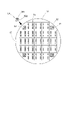
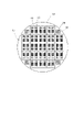
- FIG. 8 is a diagram showing an example of a wiring board 14 that constitutes a conventional probe card, showing a plane view of a probe installation surface 17 on which probes are installed.
- a large number of probe electrode pads 15 and four alignment symbols 30 are formed on the probe mounting surface 17 , and a probe 16 is attached to each probe electrode pad 15 .
- the probes 16 are arranged at positions corresponding to electrode pads of a semiconductor wafer, which is an object to be inspected.
- the alignment symbols 30 are formed on the outer peripheral edge of the wiring board 14 at approximately equal intervals.
- the probe electrode pads 15 and the alignment symbols 30 are metal films formed on the probe mounting surface 17 by photolithography using electroplating or etching.
- the alignment symbol 30 is a thin film made of a metal material having a high reflectance and having a predetermined geometrical planar shape, such as an annular Au film.
- the symbol peripheral area 31 is an area surrounding the alignment symbol 30 and has a reflectance lower than that of the alignment symbol 30 .
- FIG. (a) to (d) of FIG. 9 are diagrams showing various states that can occur in the alignment symbol 30 and the symbol surrounding area 31.
- FIG. (a) in the drawing shows the appearance of a normal alignment symbol 30 .
- (b) in the figure is an example in which a foreign object 32 adheres to the symbol peripheral area 31 . If the foreign matter 32 has a high reflectance, the alignment symbol 30 may not be correctly recognized.
- (c) in the figure is an example in which a stain 33 occurs in the symbol peripheral area 31 and variations in reflectance occur in the symbol peripheral area 31 . Also in this case, there is a possibility that the alignment symbol 30 cannot be correctly recognized.
- (d) in the figure is an example in which the alignment symbol 30 has a scratch 34 . The shape of the alignment symbol may change, and the alignment symbol 30 may not be recognized correctly.
- Patent Document 1 As a conventional method for forming alignment symbols, a method using a sheet-like member has been proposed (for example, Patent Document 1).
- Patent Document 1 after affixing a sheet-like member having a non-reflecting surface or a light diffusing surface to cover the light-reflecting surface of a wiring board, an opening is formed in the sheet-like member by laser processing to form a light-reflecting surface. describes a method of forming alignment symbols on a wiring substrate by partially exposing the .
- this method is not a method for repairing defects in the alignment symbol or the symbol peripheral area, it is considered applicable to repairing defects in the symbol peripheral area by adhering a sheet-shaped member. . However, it is still necessary to perform an opening process using a laser, and it is considered difficult to suppress the repair cost. In addition, since the opening of the sheet-like member defines the outer edge of the alignment symbol, when it is applied to the repair of the alignment symbol, the outer edge of the original alignment symbol and the opening of the sheet-like member must be completely matched. If so, it is considered that the shape of the alignment symbol is distorted.
- the present invention has been made in view of the above circumstances, and an object of the present invention is to provide an alignment chip for forming alignment symbols on the wiring substrate of a probe card. In particular, it is an object of the present invention to provide an alignment chip for repairing defects in alignment symbols or their peripheral areas.
- Another object of the present invention is to provide a probe card in which alignment symbols are formed on a wiring board using an alignment chip.
- a further object of the present invention is to provide a probe card repair method for repairing a probe card in which a defect has occurred in an alignment symbol or its peripheral area using an alignment chip.
- a probe card alignment chip comprises: a substrate having a bonding surface that is bonded via an adhesive to a probe installation surface of a wiring substrate constituting a probe card; and a bonding surface of the substrate. an alignment symbol made of a metal film formed on a symbol surface opposite to the symbol surface, the symbol surface comprising a symbol peripheral region surrounding the alignment symbol, the symbol peripheral region having a lower reflection than the alignment symbol rate.
- the probe card alignment chip according to the second embodiment of the present invention is configured such that the symbol peripheral region is formed with a resin film.
- a probe card alignment chip in addition to the above configuration, comprises a first metal layer where the metal film is exposed, and a second metal layer formed between the first metal layer and the substrate. and a metal layer, wherein the second metal layer is made of a material having a Young's modulus higher than that of the first metal layer and is formed thicker than the first metal layer.
- the substrate is configured to have a thickness of 450 ⁇ m or less.
- the probe card alignment chip according to the fifth embodiment of the present invention is, in addition to the above configuration, attached so that the alignment chip covers the alignment symbol preliminarily formed on the probe installation surface.
- a probe card comprises: a wiring substrate having a probe installation surface on which probe electrode pads are formed; probes attached to the probe electrode pads;
- the alignment chip comprises a substrate having a bonding surface to be bonded to the probe installation surface via an adhesive, and a metal film formed on the symbol surface opposite to the bonding surface of the substrate. and an alignment symbol, wherein the symbol surface comprises a symbol peripheral area surrounding the alignment symbol, the symbol peripheral area having a lower reflectance than the alignment symbol.
- a probe card repair method is a wiring having a probe mounting surface on which are formed probe electrode pads for mounting probes and first alignment symbols for alignment before inspection.
- a probe card repair method for repairing a probe card having a substrate wherein an alignment chip is attached to the probe arrangement surface using an adhesive, the alignment chip covers the first alignment symbol, and the alignment chip is covered with the first alignment symbol.
- a second alignment symbol formed on the symbol surface opposite to the wiring board is arranged to overlap the first alignment symbol.
- an alignment chip for forming alignment symbols on the wiring board of the probe card.
- an alignment chip for repairing defects in alignment symbols or their peripheral areas.
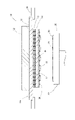
- FIG. 1 is a diagram showing an example of a schematic configuration of a probe card 10 to which alignment chips according to Embodiment 1 of the present invention are applied;
- FIG. It is the figure which showed one structural example of 5 A of alignment chips. It is the figure which showed the outline
- FIG. 10 is a diagram showing a configuration example of an alignment chip 5B according to Embodiment 2 of the present invention; 4A to 4C are diagrams sequentially showing an example of the manufacturing process of the alignment chip 5B;
- FIG. and FIG. 10 is a diagram showing an example of a wiring board that constitutes a conventional probe card.
- 3A and 3B are diagrams showing various states that can occur in an alignment symbol 30 and a symbol peripheral area 31.
- FIG. 1 is a diagram showing an example of a schematic configuration of a probe card 10 to which alignment chips according to Embodiment 1 of the present invention are applied.
- the probe card 10 is attached to the wafer prober with the probe installation surface 17 facing downward, and faces the electrode pads 21 of the semiconductor wafer 20 placed on the stage 26. By moving the stage 26 up and down, Probes 16 can be brought into contact with electrode pads 21 .
- the probe card 10 is composed of a main substrate 11, a reinforcing plate 12, an interposer 13, an ST (Space transformer) substrate 14 and two or more probes 16.
- the main board 11 is a wiring board detachably attached to the wafer prober, and for example, a disk-shaped glass epoxy board is used.
- the main board 11 is supported by a card holder 25 of a wafer prober at the outer peripheral edge of the lower surface thereof, and is arranged substantially horizontally.
- a reinforcing plate 12 for suppressing distortion of the main substrate 11 is attached to the central portion of the upper surface of the main substrate 11, and a signal terminal of a tester device (not shown) is connected to the outer peripheral edge portion of the upper surface 2.
- the above external terminals 11t are provided.
- the interposer 13 is arranged between the main board 11 and the ST board 14, and is a connection means between the boards that conducts the wiring of the main board 11 and the wiring of the ST board 14, and is equipped with, for example, a large number of pogo pins.
- the ST substrate 14 is a multi-layer wiring substrate that converts the electrode pitch, for example, a laminated plate in which two or more ceramic plates are bonded together.
- the ST substrate 14 is arranged on the lower surface side of the main substrate 11 with the interposer 13 interposed therebetween.
- the probe mounting surface 17 is the lower surface of the ST substrate 14, and is formed with a large number of probe electrode pads 15 and four alignment symbols 30. As shown in FIG.
- the probe electrode pads 15 and the alignment symbols 30 are metal films formed on the probe installation surface 17 by photolithography using electroplating or etching.
- the probe electrode pads 15 are electrodes to which probes are connected, and are formed so as to correspond to the electrode pads 21 on the semiconductor wafer 20 .
- the stage 26 is a mounting table for the semiconductor wafer 20, and is capable of moving and rotating in the horizontal plane and moving in the vertical direction.
- the camera 27 is an image capturing means for capturing an image of the alignment symbol 30 . By capturing an image while moving the stage 26 , the position of the alignment symbol 30 is detected and the semiconductor wafer 20 is aligned with the probe card 10 .
- FIG. 2 is a diagram showing one configuration example of the alignment chip 5A.
- (a) is a plan view of the symbol surface
- (b) is a diagram cut along the AA cutting line.
- 1 is a cross-sectional view (cross-sectional view taken along the line AA).
- the alignment chip 5A is a repair member for repairing the probe card 10, and has a symbol surface on which the alignment symbol 501 is formed and a surface opposite to the symbol surface, which is attached to the ST substrate 14. and The symbol surface is divided into an alignment symbol 501, which is a high reflectance area, and a symbol peripheral area 502, which is a low reflectance area.
- the alignment symbol 501 is a thin film made of a metal material having a high reflectance and having a predetermined geometrical planar shape, such as an annular Au film.
- the planar shape of the alignment symbol 501 is desirably the same as the original alignment symbol 30 formed on the ST substrate 14, and the metal material and surface condition are also desirably the same.
- the alignment symbol 501 is a thin film made of a metal material having a high reflectance and having a predetermined geometrical planar shape, such as an annular Au film.
- the planar shape of the alignment symbol 501 is desirably the same as the original alignment symbol 30 formed on the ST substrate 14, and the metal material and surface condition are also desirably the same.
- the symbol peripheral area 502 is made of a resin material having a low reflectance, and is a thin film formed in an area other than the alignment symbol 501, such as a polyimide film.
- the symbol surrounding area 502 is an area surrounding at least the alignment symbol 501, and is also formed in the hollow area when the alignment symbol 501 has a hollow area such as when the alignment symbol 501 has an annular shape.
- the alignment chip 5A includes a ceramic or silicon substrate 51, a metal film 52 corresponding to an alignment symbol 501 formed on the substrate 51, and a symbol periphery formed on the substrate 51. and a resin film 53 corresponding to the region 502 .
- the metal film 52 can be composed of one or more metal layers, and the resin film 53 can also be composed of one or more resin layers.
- the alignment chip 5A must have a thickness that does not contact the semiconductor chip wafer during inspection. During inspection, the semiconductor wafer 20 is brought closer to the probes 16, and after reaching the position where the tips of the probes 16 start contacting the electrode pads 21 of the semiconductor wafer 20, the probes 16 are brought closer by a certain distance, and the probes 16 are elastically deformed. drive takes place. Therefore, it is necessary to prevent the alignment chip 5A attached to the probe mounting surface from exceeding the height of the probe 16 elastically deformed by the overdrive.
- the thickness of the alignment chip is desirably 500 ⁇ m or less
- the thickness of the substrate 51 is desirably 450 ⁇ m or less
- the film thickness of the metal film 52 and the resin film 53 is desirably 50 ⁇ m or less.
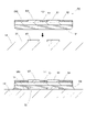
- FIGS. 3 and 4 are diagrams showing an example of a probe card repair method using the alignment chip 5A.
- Fig. 3 shows an overview of the probe card repair method.
- the illustrated ST substrate 14 has a defect in which a foreign substance 32 with a high reflectance adheres to one of the symbol peripheral regions 31 . Therefore, the ST substrate 14 is repaired by attaching the alignment chip 5A.
- the ST substrate 14 to be repaired is preferably the one before the probes 16 are attached, but it may be the one after the probes 16 are attached.
- FIG. 4 is a cross-sectional view taken perpendicular to the alignment chip 5A, (a) showing a cross-sectional view before repair, and (b) showing a cross-sectional view after repair.
- the alignment chip 5A is attached onto the probe mounting surface of the ST substrate 14 via an adhesive 54 to cover the alignment symbol 30 and the symbol peripheral area 31 with the defect.
- the alignment chip 5A After applying the adhesive 54 to the attachment surface of the alignment chip 5A, the alignment chip 5A is attached to a predetermined position on the ST substrate 14 while performing accurate alignment with the ST substrate 14.
- the alignment chip 5A is attached so that the alignment symbol 501 matches the original alignment symbol 30 on the ST substrate 14. However, when pasted, the original alignment symbol 30 is hidden by the alignment chip 5A to be pasted. For this reason, the alignment chip 5A is attached while aligning the target mark of the microscope with the attachment position of the alignment chip 5A on the ST substrate 14 and looking through the eyepiece of the microscope.
- Alignment of the alignment chip 5A is performed using, for example, a stage on which XY-direction micrometers are attached, and a Hisomet (optical focal position detection type non-contact step measuring microscope).
- the ST substrate 14 placed on the stage is observed by Hisomet, and the tip of the probe 16 is aligned with the target mark.
- the target mark indicates the sticking position of the alignment chip 5A.
- the alignment chip 5A is pasted while looking through the Hisomet eyepiece.
- FIGS. 5A to 5F are diagrams sequentially showing an example of the manufacturing process of the alignment chip 5A.
- FIG. 5(a) shows a state in which a photoresist 60 is selectively formed on a substrate 51.
- FIG. After the photoresist 60 is formed on the entire surface of the substrate 51 , selective exposure and development are performed to leave only the area corresponding to the alignment symbol 501 , and the area corresponding to the symbol peripheral area 502 is covered with the substrate 51 .
- An opening 601 is formed to expose the .
- FIG. 5(b) shows a state in which the resin layer 61 is selectively formed on the substrate 51.
- FIG. A resin layer 61 is formed on a substrate 51 on which a photoresist 60 is selectively formed, and the photoresist 60 is removed to leave only the region corresponding to the symbol peripheral region 502 of the resin layer 61, which is an alignment symbol.
- An opening 602 exposing the substrate 51 is formed in a region corresponding to 501 .
- FIG. 5(c) shows a state in which the seed layer 62 is formed over the entire surface of the substrate 51.
- FIG. Seed layer 62 is a thin metal layer formed by sputtering.
- FIG. 5(d) shows a state in which the first metal layer 630 is formed on the entire surface of the substrate 51 by electroplating.
- a metal material having a relatively large Young's modulus such as copper (Cu) or a nickel-cobalt alloy (NiCo), is used for the first metal layer 630 .
- FIG. 5(e) shows a state in which the entire surface of the substrate 51 on which the first metal layer 630 is formed is polished.
- the polishing process planarizes the surface of the substrate 51 . This polishing process is performed until the resin layer 61 is exposed, and the first metal layer 630 is removed from the area corresponding to the symbol peripheral area 502 while being exposed in the area corresponding to the alignment symbol 501 . Become.
- FIG. 5(f) shows a state in which a second metal layer 631 and a third metal layer 632 are formed in order in a region corresponding to the alignment symbol 501.
- FIG. The second metal layer 631 and the third metal layer 632 are formed by electroplating.
- a metal material having a high reflectance, such as gold (Au) is used for the exposed third metal layer 632 .
- the seed layer 62 and the first to third metal layers 630 to 632 constitute the metal film 52 .
- the first metal layer 630 is made of a metal material having a higher Young's modulus than the third metal layer 632 and is formed as a layer thicker than the third metal layer 632 . Therefore, the mechanical strength of the alignment chip 5A can be ensured as compared with the case where the metal film 52 is composed only of the metal material of the third metal layer 632, for example.
- the alignment chip 5A can be formed by subjecting the substrate 51 to photolithography. Therefore, it can be easily manufactured using existing manufacturing techniques. Further, after forming a large number of alignment chips 5A on the same substrate 51 at the same time, the alignment chips 5A can be separated by dicing. Therefore, the alignment chip 5A can be manufactured at low cost. In addition, unlike the prior art, laser processing is not required after attachment to the ST substrate 14, and the wiring substrate can be easily and inexpensively repaired.
- Embodiment 2 As another example of the alignment chip 5A, an example of an alignment chip 5B having a different shape of the alignment symbol 501 and a different manufacturing method will be described. In this embodiment, differences from the alignment chip 5A will be mainly described, and redundant description will be omitted.
- Alignment chip 5B 6A and 6B are diagrams showing one configuration example of the alignment chip 5B according to the second embodiment, in which (a) is a plan view of the symbol surface, and (b) is a BB section.
- FIG. 4 is a cross-sectional view (BB cross-sectional view) showing a state when cut along a line;
- the alignment symbol 501 has a cross-shaped planar shape composed of two rectangles orthogonal to each other.
- the alignment chip 5A includes a ceramic or silicon substrate 51, a base metal film 55 formed on the substrate 51, a metal film 52 and a resin film formed on the base metal film 55. 53.
- the base metal film 55 can be composed of one or more metal layers.
- FIGS. 7A to 7D are diagrams sequentially showing an example of a manufacturing process of the alignment chip 5B.
- FIG. 7A shows a state in which the base metal film 55 is formed over the entire surface of the substrate 51 .
- a metal material having a relatively large Young's modulus, such as copper (Cu), is used for the base metal film 55 .
- FIG. 7(b) shows a state in which a photoresist 60 is selectively formed on the base metal film 55.
- An opening 601 is formed exposing the membrane 55 .
- FIG. 7(c) shows a state in which the resin layer 61 is selectively formed on the base metal film 55.
- FIG. A resin layer 61 is formed on a substrate 51 on which a photoresist 60 is selectively formed, and the photoresist 60 is removed to leave only the region corresponding to the symbol peripheral region 502 of the resin layer 61, which is an alignment symbol.
- An opening 602 exposing the base metal film 55 is formed in a region corresponding to 501 .
- FIG. 7(d) shows a state in which a second metal layer 631 and a third metal layer 632 are sequentially formed in the region corresponding to the alignment symbol 501.
- the second metal layer 631 and the third metal layer 632 are formed by electroplating.
- a metal material having a high reflectance, such as gold (Au), is used for the exposed third metal layer 632 .
- the second and third metal layers 631 and 632 constitute the metal film 52 .
- the base metal film 55 is made of a metal material having a Young's modulus larger than that of the third metal layer 632 and formed as a layer thicker than the third metal layer 632 .
- the alignment symbol 501 is composed of the metal film 52 and a part of the base metal film 55 that overlaps with the metal film 52, and the metal film that constitutes the alignment symbol 501 is, for example, only the metal material of the third metal layer 632. The mechanical strength of the alignment chip 5B can be ensured compared to the case of the configuration.
- the shape of the alignment symbol 501 is an annular shape and a cross shape has been described, but the present invention is not limited to such cases. Any shape can be adopted as the inheritance of the alignment symbol 501 .
- the alignment chip 5A or 5B when there is a defect in the alignment symbol 30 or the symbol peripheral area 31 formed on the ST substrate 14, the alignment chip 5A or 5B is attached to repair the defect.
- the invention is not limited to only such cases.
- the alignment chip 5A or 5B can be attached to the ST substrate 14 on which the alignment symbol 30 is not formed, and the alignment symbol 501 can be additionally formed after the ST substrate 14 is manufactured.
- the alignment chips 5A and 5B are desirably attached to the ST substrate 14 before the probes 16 are attached, but they can also be attached to the ST substrate 14 after the probes 16 are attached. Moreover, although it is desirable that the alignment chips 5A and 5B completely cover the original alignment symbol 30, they do not have to completely cover the original symbol peripheral region 31. FIG.
- probe card 11 main substrate 13 interposer 14 ST substrate (wiring substrate) 15 probe electrode pad 16 probe 17 probe mounting surface 20 semiconductor wafer 21 electrode pad 30 alignment symbol 31 symbol peripheral regions 5A, 5B alignment chip 501 alignment symbol 502 symbol peripheral region 51 substrate 52 metal film 53 resin film 54 adhesive 55 base metal Film 60 Photoresist 601, 602 Opening 61 Resin layer 62 Seed layer
Landscapes
- Physics & Mathematics (AREA)
- General Physics & Mathematics (AREA)
- Engineering & Computer Science (AREA)
- Computer Hardware Design (AREA)
- Microelectronics & Electronic Packaging (AREA)
- General Engineering & Computer Science (AREA)
- Measuring Leads Or Probes (AREA)
- Testing Or Measuring Of Semiconductors Or The Like (AREA)
Priority Applications (6)
| Application Number | Priority Date | Filing Date | Title |
|---|---|---|---|
| CN202180062337.3A CN116194784A (zh) | 2021-02-19 | 2021-02-19 | 探针卡用对准芯片、探针卡以及探针卡修补方法 |
| PCT/JP2021/006256 WO2022176143A1 (ja) | 2021-02-19 | 2021-02-19 | プローブカード用アライメントチップ、プローブカード及びプローブカード補修方法 |
| JP2023500448A JP7459368B2 (ja) | 2021-02-19 | 2021-02-19 | プローブカード用アライメントチップ、プローブカード及びプローブカード補修方法 |
| US18/265,263 US12596147B2 (en) | 2021-02-19 | 2021-02-19 | Alignment chip for probe card, probe card and probe card repair method |
| KR1020237007418A KR102876398B1 (ko) | 2021-02-19 | 2021-02-19 | 프로브 카드용 얼라이먼트 칩, 프로브 카드 및 프로브 카드 보수 방법 |
| TW110134210A TWI918717B (zh) | 2021-02-19 | 2021-09-14 | 對準晶片、探針卡及探針卡修補方法 |
Applications Claiming Priority (1)
| Application Number | Priority Date | Filing Date | Title |
|---|---|---|---|
| PCT/JP2021/006256 WO2022176143A1 (ja) | 2021-02-19 | 2021-02-19 | プローブカード用アライメントチップ、プローブカード及びプローブカード補修方法 |
Publications (1)
| Publication Number | Publication Date |
|---|---|
| WO2022176143A1 true WO2022176143A1 (ja) | 2022-08-25 |
Family
ID=82930435
Family Applications (1)
| Application Number | Title | Priority Date | Filing Date |
|---|---|---|---|
| PCT/JP2021/006256 Ceased WO2022176143A1 (ja) | 2021-02-19 | 2021-02-19 | プローブカード用アライメントチップ、プローブカード及びプローブカード補修方法 |
Country Status (5)
| Country | Link |
|---|---|
| US (1) | US12596147B2 (https=) |
| JP (1) | JP7459368B2 (https=) |
| KR (1) | KR102876398B1 (https=) |
| CN (1) | CN116194784A (https=) |
| WO (1) | WO2022176143A1 (https=) |
Cited By (1)
| Publication number | Priority date | Publication date | Assignee | Title |
|---|---|---|---|---|
| US12467953B2 (en) | 2021-03-15 | 2025-11-11 | Japan Electronic Materials Corporation | Probe card |
Citations (8)
| Publication number | Priority date | Publication date | Assignee | Title |
|---|---|---|---|---|
| JPH0196944A (ja) * | 1987-10-08 | 1989-04-14 | Nec Corp | 高周波特性測定装置 |
| JPH11154694A (ja) * | 1997-11-21 | 1999-06-08 | Matsushita Electric Ind Co Ltd | ウェハ一括型測定検査用アライメント方法およびプローブカードの製造方法 |
| JP2001330626A (ja) * | 2000-05-22 | 2001-11-30 | Micronics Japan Co Ltd | プローブカード及びこれにアライメントマークを形成する方法 |
| US6429671B1 (en) * | 1998-11-25 | 2002-08-06 | Advanced Micro Devices, Inc. | Electrical test probe card having a removable probe head assembly with alignment features and a method for aligning the probe head assembly to the probe card |
| JP2007184417A (ja) * | 2006-01-06 | 2007-07-19 | Kawasaki Microelectronics Kk | プローブカードの取り付け位置ずれの検出方法及びプローバ装置 |
| WO2008120575A1 (ja) * | 2007-04-03 | 2008-10-09 | Advantest Corporation | コンタクタの実装方法 |
| JP2011117761A (ja) * | 2009-12-01 | 2011-06-16 | Japan Electronic Materials Corp | プローブカードおよびプローブカードの製造方法 |
| JP2017118138A (ja) * | 2017-02-23 | 2017-06-29 | ルネサスエレクトロニクス株式会社 | 半導体装置の製造方法 |
Family Cites Families (18)
| Publication number | Priority date | Publication date | Assignee | Title |
|---|---|---|---|---|
| JPH1096944A (ja) * | 1996-09-25 | 1998-04-14 | Toshiba Electron Eng Corp | 電気的接続構造および液晶表示装置 |
| GB9826596D0 (en) | 1998-12-04 | 1999-01-27 | P J O Ind Limited | Conductive materials |
| JP2000346875A (ja) | 1999-06-07 | 2000-12-15 | Advantest Corp | プローブカードおよびこれを用いたic試験装置 |
| JP2006078351A (ja) * | 2004-09-10 | 2006-03-23 | Matsushita Electric Ind Co Ltd | プローブカード |
| JP4187718B2 (ja) * | 2004-12-20 | 2008-11-26 | 松下電器産業株式会社 | プローブカード |
| JP2007071699A (ja) * | 2005-09-07 | 2007-03-22 | Rika Denshi Co Ltd | 垂直型プローブカード |
| JP2014146829A (ja) * | 2005-11-10 | 2014-08-14 | Renesas Electronics Corp | 半導体チップおよび半導体装置 |
| JP2007200934A (ja) * | 2006-01-23 | 2007-08-09 | Fujitsu Ltd | プローブカードのプローブ針の針跡評価方法 |
| WO2007092593A2 (en) * | 2006-02-08 | 2007-08-16 | Sv Probe Pte Ltd. | Probe repair methods |
| JP5199859B2 (ja) | 2008-12-24 | 2013-05-15 | 株式会社日本マイクロニクス | プローブカード |
| JP2011075532A (ja) * | 2009-10-02 | 2011-04-14 | Japan Electronic Materials Corp | プローブカード及びその製造方法 |
| JP2011204889A (ja) * | 2010-03-25 | 2011-10-13 | Kyocera Corp | インターポーザ基板 |
| JP5297491B2 (ja) * | 2011-03-23 | 2013-09-25 | ルネサスエレクトロニクス株式会社 | 半導体装置 |
| JP5847663B2 (ja) * | 2012-08-01 | 2016-01-27 | 日本電子材料株式会社 | プローブカード用ガイド板の製造方法 |
| US10529593B2 (en) * | 2018-04-27 | 2020-01-07 | Taiwan Semiconductor Manufacturing Co., Ltd. | Semiconductor package comprising molding compound having extended portion and manufacturing method of semiconductor package |
| TW202022386A (zh) | 2018-12-04 | 2020-06-16 | 蔚華科技股份有限公司 | 測試半導體設備之方法及結構 |
| CN116547543B (zh) * | 2021-03-15 | 2026-01-27 | 日本电子材料株式会社 | 探针卡 |
| KR102760918B1 (ko) * | 2021-04-23 | 2025-02-03 | 재팬 일렉트로닉 메트리얼스 코오포레이숀 | 프로브 카드 및 프로브 카드 보수 방법 |
-
2021
- 2021-02-19 KR KR1020237007418A patent/KR102876398B1/ko active Active
- 2021-02-19 CN CN202180062337.3A patent/CN116194784A/zh active Pending
- 2021-02-19 JP JP2023500448A patent/JP7459368B2/ja active Active
- 2021-02-19 WO PCT/JP2021/006256 patent/WO2022176143A1/ja not_active Ceased
- 2021-02-19 US US18/265,263 patent/US12596147B2/en active Active
Patent Citations (8)
| Publication number | Priority date | Publication date | Assignee | Title |
|---|---|---|---|---|
| JPH0196944A (ja) * | 1987-10-08 | 1989-04-14 | Nec Corp | 高周波特性測定装置 |
| JPH11154694A (ja) * | 1997-11-21 | 1999-06-08 | Matsushita Electric Ind Co Ltd | ウェハ一括型測定検査用アライメント方法およびプローブカードの製造方法 |
| US6429671B1 (en) * | 1998-11-25 | 2002-08-06 | Advanced Micro Devices, Inc. | Electrical test probe card having a removable probe head assembly with alignment features and a method for aligning the probe head assembly to the probe card |
| JP2001330626A (ja) * | 2000-05-22 | 2001-11-30 | Micronics Japan Co Ltd | プローブカード及びこれにアライメントマークを形成する方法 |
| JP2007184417A (ja) * | 2006-01-06 | 2007-07-19 | Kawasaki Microelectronics Kk | プローブカードの取り付け位置ずれの検出方法及びプローバ装置 |
| WO2008120575A1 (ja) * | 2007-04-03 | 2008-10-09 | Advantest Corporation | コンタクタの実装方法 |
| JP2011117761A (ja) * | 2009-12-01 | 2011-06-16 | Japan Electronic Materials Corp | プローブカードおよびプローブカードの製造方法 |
| JP2017118138A (ja) * | 2017-02-23 | 2017-06-29 | ルネサスエレクトロニクス株式会社 | 半導体装置の製造方法 |
Cited By (1)
| Publication number | Priority date | Publication date | Assignee | Title |
|---|---|---|---|---|
| US12467953B2 (en) | 2021-03-15 | 2025-11-11 | Japan Electronic Materials Corporation | Probe card |
Also Published As
| Publication number | Publication date |
|---|---|
| KR102876398B1 (ko) | 2025-10-24 |
| JP7459368B2 (ja) | 2024-04-01 |
| US12596147B2 (en) | 2026-04-07 |
| TW202234067A (zh) | 2022-09-01 |
| CN116194784A (zh) | 2023-05-30 |
| JPWO2022176143A1 (https=) | 2022-08-25 |
| US20240103071A1 (en) | 2024-03-28 |
| KR20230044303A (ko) | 2023-04-03 |
Similar Documents
| Publication | Publication Date | Title |
|---|---|---|
| US20020186030A1 (en) | Contact probe and probe device | |
| JP2002110751A (ja) | 半導体集積回路装置の検査装置および製造方法 | |
| JPH11174118A (ja) | 集積回路チップ検査用プロブカード | |
| JP7202550B1 (ja) | プローブカード | |
| JP2010276541A (ja) | 薄膜プローブシートおよびその製造方法、プローブカード、ならびに半導体チップ検査装置 | |
| KR20000047438A (ko) | 반도체 시험 방법 및 반도체 시험 장치 | |
| US12339314B2 (en) | Probe card and method for repairing probe card | |
| JP7459368B2 (ja) | プローブカード用アライメントチップ、プローブカード及びプローブカード補修方法 | |
| KR101955663B1 (ko) | 프로브 카드용의 범프 부착 멤브레인 시트, 프로브 카드 및 프로브 카드용의 범프 부착 멤브레인 시트의 제조방법 | |
| JP2011054630A (ja) | 検査用プローブおよび検査用プローブの製造方法 | |
| JP4830772B2 (ja) | 半導体チップの検査方法 | |
| KR101954187B1 (ko) | 마이크로콘택트 핀 어셈블리 제조방법 | |
| TWI918717B (zh) | 對準晶片、探針卡及探針卡修補方法 | |
| TWI921511B (zh) | 探針卡及探針卡的修補方法 | |
| KR101540972B1 (ko) | 디스플레이 패널 검사용 프로브 블록의 제조 방법 | |
| JP5530191B2 (ja) | 電気的試験用プローブ及びその製造方法、並びに電気的接続装置及びその製造方法 | |
| JPH09159694A (ja) | Lsiテストプローブ装置 | |
| JP2000164652A (ja) | ウエハ一括コンタクトボード用多層配線基板、該多層配線基板に接続するコネクタ、及びそれらの接続構造、並びに検査装置 | |
| JPH1116961A (ja) | 屈曲部を有する金属体およびその成形方法と前記金属体を用いたコンタクトプローブおよびその製造方法 | |
| JP4406218B2 (ja) | プローブを備えた検査装置、およびプローブを備えた検査装置の位置決め機構による位置決め方法 | |
| KR101058513B1 (ko) | 프로브 카드의 제조 방법 | |
| JPH11352151A (ja) | コンタクトプローブおよびそれを備えたプローブ装置並びにコンタクトプローブの製造方法 | |
| JPH11121562A (ja) | バンプ検査方法 | |
| JP2006078351A (ja) | プローブカード | |
| JPH0833415B2 (ja) | プローブカード |
Legal Events
| Date | Code | Title | Description |
|---|---|---|---|
| 121 | Ep: the epo has been informed by wipo that ep was designated in this application |
Ref document number: 21926576 Country of ref document: EP Kind code of ref document: A1 |
|
| ENP | Entry into the national phase |
Ref document number: 2023500448 Country of ref document: JP Kind code of ref document: A |
|
| ENP | Entry into the national phase |
Ref document number: 20237007418 Country of ref document: KR Kind code of ref document: A |
|
| WWE | Wipo information: entry into national phase |
Ref document number: 18265263 Country of ref document: US |
|
| NENP | Non-entry into the national phase |
Ref country code: DE |
|
| WWE | Wipo information: entry into national phase |
Ref document number: 11202304233W Country of ref document: SG |
|
| 122 | Ep: pct application non-entry in european phase |
Ref document number: 21926576 Country of ref document: EP Kind code of ref document: A1 |
|
| WWG | Wipo information: grant in national office |
Ref document number: 18265263 Country of ref document: US |