WO2022168217A1 - 半導体基板の製造方法および半導体装置の製造方法 - Google Patents
半導体基板の製造方法および半導体装置の製造方法 Download PDFInfo
- Publication number
- WO2022168217A1 WO2022168217A1 PCT/JP2021/004035 JP2021004035W WO2022168217A1 WO 2022168217 A1 WO2022168217 A1 WO 2022168217A1 JP 2021004035 W JP2021004035 W JP 2021004035W WO 2022168217 A1 WO2022168217 A1 WO 2022168217A1
- Authority
- WO
- WIPO (PCT)
- Prior art keywords
- substrate
- nitride semiconductor
- semiconductor layer
- reversible adhesive
- adhesive layer
- Prior art date
- Legal status (The legal status is an assumption and is not a legal conclusion. Google has not performed a legal analysis and makes no representation as to the accuracy of the status listed.)
- Ceased
Links
Images



Classifications
-
- H—ELECTRICITY
- H10—SEMICONDUCTOR DEVICES; ELECTRIC SOLID-STATE DEVICES NOT OTHERWISE PROVIDED FOR
- H10P—GENERIC PROCESSES OR APPARATUS FOR THE MANUFACTURE OR TREATMENT OF DEVICES COVERED BY CLASS H10
- H10P72/00—Handling or holding of wafers, substrates or devices during manufacture or treatment thereof
- H10P72/70—Handling or holding of wafers, substrates or devices during manufacture or treatment thereof for supporting or gripping
- H10P72/74—Handling or holding of wafers, substrates or devices during manufacture or treatment thereof for supporting or gripping using temporarily an auxiliary support
- H10P72/7402—Wafer tapes, e.g. grinding or dicing support tapes
-
- H—ELECTRICITY
- H10—SEMICONDUCTOR DEVICES; ELECTRIC SOLID-STATE DEVICES NOT OTHERWISE PROVIDED FOR
- H10P—GENERIC PROCESSES OR APPARATUS FOR THE MANUFACTURE OR TREATMENT OF DEVICES COVERED BY CLASS H10
- H10P14/00—Formation of materials, e.g. in the shape of layers or pillars
- H10P14/20—Formation of materials, e.g. in the shape of layers or pillars of semiconductor materials
- H10P14/34—Deposited materials, e.g. layers
- H10P14/3402—Deposited materials, e.g. layers characterised by the chemical composition
- H10P14/3414—Deposited materials, e.g. layers characterised by the chemical composition being group IIIA-VIA materials
- H10P14/3416—Nitrides
-
- H—ELECTRICITY
- H10—SEMICONDUCTOR DEVICES; ELECTRIC SOLID-STATE DEVICES NOT OTHERWISE PROVIDED FOR
- H10P—GENERIC PROCESSES OR APPARATUS FOR THE MANUFACTURE OR TREATMENT OF DEVICES COVERED BY CLASS H10
- H10P34/00—Irradiation with electromagnetic or particle radiation of wafers, substrates or parts of devices
- H10P34/40—Irradiation with electromagnetic or particle radiation of wafers, substrates or parts of devices with high-energy radiation
- H10P34/42—Irradiation with electromagnetic or particle radiation of wafers, substrates or parts of devices with high-energy radiation with electromagnetic radiation, e.g. laser annealing
- H10P34/422—Irradiation with electromagnetic or particle radiation of wafers, substrates or parts of devices with high-energy radiation with electromagnetic radiation, e.g. laser annealing using incoherent radiation
-
- H—ELECTRICITY
- H10—SEMICONDUCTOR DEVICES; ELECTRIC SOLID-STATE DEVICES NOT OTHERWISE PROVIDED FOR
- H10D—INORGANIC ELECTRIC SEMICONDUCTOR DEVICES
- H10D30/00—Field-effect transistors [FET]
- H10D30/01—Manufacture or treatment
- H10D30/015—Manufacture or treatment of FETs having heterojunction interface channels or heterojunction gate electrodes, e.g. HEMT
-
- H—ELECTRICITY
- H10—SEMICONDUCTOR DEVICES; ELECTRIC SOLID-STATE DEVICES NOT OTHERWISE PROVIDED FOR
- H10D—INORGANIC ELECTRIC SEMICONDUCTOR DEVICES
- H10D62/00—Semiconductor bodies, or regions thereof, of devices having potential barriers
- H10D62/80—Semiconductor bodies, or regions thereof, of devices having potential barriers characterised by the materials
- H10D62/85—Semiconductor bodies, or regions thereof, of devices having potential barriers characterised by the materials being Group III-V materials, e.g. GaAs
- H10D62/8503—Nitride Group III-V materials, e.g. AlN or GaN
-
- H—ELECTRICITY
- H10—SEMICONDUCTOR DEVICES; ELECTRIC SOLID-STATE DEVICES NOT OTHERWISE PROVIDED FOR
- H10P—GENERIC PROCESSES OR APPARATUS FOR THE MANUFACTURE OR TREATMENT OF DEVICES COVERED BY CLASS H10
- H10P10/00—Bonding of wafers, substrates or parts of devices
- H10P10/12—Bonding of semiconductor wafers or semiconductor substrates to semiconductor wafers or semiconductor substrates
-
- H—ELECTRICITY
- H10—SEMICONDUCTOR DEVICES; ELECTRIC SOLID-STATE DEVICES NOT OTHERWISE PROVIDED FOR
- H10P—GENERIC PROCESSES OR APPARATUS FOR THE MANUFACTURE OR TREATMENT OF DEVICES COVERED BY CLASS H10
- H10P14/00—Formation of materials, e.g. in the shape of layers or pillars
- H10P14/20—Formation of materials, e.g. in the shape of layers or pillars of semiconductor materials
-
- H—ELECTRICITY
- H10—SEMICONDUCTOR DEVICES; ELECTRIC SOLID-STATE DEVICES NOT OTHERWISE PROVIDED FOR
- H10P—GENERIC PROCESSES OR APPARATUS FOR THE MANUFACTURE OR TREATMENT OF DEVICES COVERED BY CLASS H10
- H10P90/00—Preparation of wafers not covered by a single main group of this subclass, e.g. wafer reinforcement
-
- H—ELECTRICITY
- H10—SEMICONDUCTOR DEVICES; ELECTRIC SOLID-STATE DEVICES NOT OTHERWISE PROVIDED FOR
- H10P—GENERIC PROCESSES OR APPARATUS FOR THE MANUFACTURE OR TREATMENT OF DEVICES COVERED BY CLASS H10
- H10P72/00—Handling or holding of wafers, substrates or devices during manufacture or treatment thereof
- H10P72/70—Handling or holding of wafers, substrates or devices during manufacture or treatment thereof for supporting or gripping
- H10P72/74—Handling or holding of wafers, substrates or devices during manufacture or treatment thereof for supporting or gripping using temporarily an auxiliary support
- H10P72/7434—Handling or holding of wafers, substrates or devices during manufacture or treatment thereof for supporting or gripping using temporarily an auxiliary support used in a transfer process involving at least two transfer steps, i.e. including an intermediate handle substrate
-
- H—ELECTRICITY
- H10—SEMICONDUCTOR DEVICES; ELECTRIC SOLID-STATE DEVICES NOT OTHERWISE PROVIDED FOR
- H10P—GENERIC PROCESSES OR APPARATUS FOR THE MANUFACTURE OR TREATMENT OF DEVICES COVERED BY CLASS H10
- H10P72/00—Handling or holding of wafers, substrates or devices during manufacture or treatment thereof
- H10P72/70—Handling or holding of wafers, substrates or devices during manufacture or treatment thereof for supporting or gripping
- H10P72/74—Handling or holding of wafers, substrates or devices during manufacture or treatment thereof for supporting or gripping using temporarily an auxiliary support
- H10P72/744—Details of chemical or physical process used for separating the auxiliary support from a device or a wafer
-
- H—ELECTRICITY
- H10—SEMICONDUCTOR DEVICES; ELECTRIC SOLID-STATE DEVICES NOT OTHERWISE PROVIDED FOR
- H10P—GENERIC PROCESSES OR APPARATUS FOR THE MANUFACTURE OR TREATMENT OF DEVICES COVERED BY CLASS H10
- H10P90/00—Preparation of wafers not covered by a single main group of this subclass, e.g. wafer reinforcement
- H10P90/19—Preparing inhomogeneous wafers
- H10P90/1904—Preparing vertically inhomogeneous wafers
- H10P90/1906—Preparing SOI wafers
- H10P90/1914—Preparing SOI wafers using bonding
Definitions
- Patent Document 1 can also be applied to a technique of transferring a nitride semiconductor layer onto a different substrate such as a diamond substrate.
- diamond is a material that is difficult to manufacture and has low workability
- diamond substrates have lower qualities such as the amount of warpage and the uniformity of substrate thickness compared to Si substrates and SiC substrates. There is a tendency.
- the step of bonding the diamond substrate to the upper surface of the nitride semiconductor layer transferred onto the support substrate if the diamond substrate warps greatly or the thickness of the diamond substrate is non-uniform, it is difficult to apply pressure for bonding. Pressure is not applied uniformly over the entire surface of the diamond substrate, making it difficult to uniformly bond the nitride semiconductor layer and the diamond substrate over the entire surface.
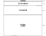
- the reversible adhesive layer 4 is cured for the purpose of improving the mechanical strength of the reversible adhesive layer 4 .
- the curing conditions for the reversible adhesive layer 4 differ depending on the reversible adhesive that constitutes it.
- the reversible adhesive layer 4 can be cured by irradiating visible light having a wavelength in the range of 420 nm to 600 nm. Glass, sapphire, silicon, SiC, or the like can be used as the material of the support substrate 5.
- the reversible adhesive layer 4 is switched between the cured state and the softened state by light irradiation, the reversible adhesive layer 4 It is necessary to use materials that are transparent to the light used for curing and softening.
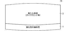
- the method of manufacturing the semiconductor substrate 10 according to the second embodiment is the same as that of the first embodiment except that semiconductor elements are formed in advance on the nitride semiconductor layer 1 used in the first step. 2 to 9 shown in the first embodiment are also referred to in the following description of the method for manufacturing the semiconductor substrate 10 according to the second embodiment. Further, explanations overlapping with those of the first embodiment will be omitted as appropriate.
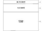
- the reversible adhesive layer 4 is subjected to a softening process as shown in FIG. 8, a process for recuring the reversible adhesive layer 4 is performed. Then, the pressure for forming a bond between the nitride semiconductor layer 1 and the new substrate 2 is released, and the sample (the structure shown in FIG. 8) is taken out from the bonding apparatus.
Landscapes
- Recrystallisation Techniques (AREA)
Priority Applications (6)
| Application Number | Priority Date | Filing Date | Title |
|---|---|---|---|
| JP2022579226A JP7475503B2 (ja) | 2021-02-04 | 2021-02-04 | 半導体基板の製造方法および半導体装置の製造方法 |
| EP21924614.7A EP4290553A4 (en) | 2021-02-04 | 2021-02-04 | METHOD FOR PRODUCING A SEMICONDUCTOR SUBSTRATE AND METHOD FOR PRODUCING A SEMICONDUCTOR COMPONENT |
| KR1020237021787A KR102760469B1 (ko) | 2021-02-04 | 2021-02-04 | 반도체 기판의 제조 방법 및 반도체 장치의 제조 방법 |
| US18/265,434 US20240030055A1 (en) | 2021-02-04 | 2021-02-04 | Method of manufacturing semiconductor substrate and method of manufacturing semiconductor device |
| CN202180092263.8A CN116868309A (zh) | 2021-02-04 | 2021-02-04 | 半导体基板的制造方法及半导体装置的制造方法 |
| PCT/JP2021/004035 WO2022168217A1 (ja) | 2021-02-04 | 2021-02-04 | 半導体基板の製造方法および半導体装置の製造方法 |
Applications Claiming Priority (1)
| Application Number | Priority Date | Filing Date | Title |
|---|---|---|---|
| PCT/JP2021/004035 WO2022168217A1 (ja) | 2021-02-04 | 2021-02-04 | 半導体基板の製造方法および半導体装置の製造方法 |
Publications (1)
| Publication Number | Publication Date |
|---|---|
| WO2022168217A1 true WO2022168217A1 (ja) | 2022-08-11 |
Family
ID=82740968
Family Applications (1)
| Application Number | Title | Priority Date | Filing Date |
|---|---|---|---|
| PCT/JP2021/004035 Ceased WO2022168217A1 (ja) | 2021-02-04 | 2021-02-04 | 半導体基板の製造方法および半導体装置の製造方法 |
Country Status (6)
| Country | Link |
|---|---|
| US (1) | US20240030055A1 (https=) |
| EP (1) | EP4290553A4 (https=) |
| JP (1) | JP7475503B2 (https=) |
| KR (1) | KR102760469B1 (https=) |
| CN (1) | CN116868309A (https=) |
| WO (1) | WO2022168217A1 (https=) |
Citations (7)
| Publication number | Priority date | Publication date | Assignee | Title |
|---|---|---|---|---|
| JPH06268183A (ja) | 1993-03-15 | 1994-09-22 | Fujitsu Ltd | 半導体装置の製造方法 |
| JP2014239179A (ja) * | 2013-06-10 | 2014-12-18 | 日本電信電話株式会社 | 窒化物半導体装置の製造方法 |
| WO2017119412A1 (ja) * | 2016-01-07 | 2017-07-13 | 国立研究開発法人産業技術総合研究所 | 光可逆接着剤 |
| WO2018143344A1 (ja) * | 2017-02-02 | 2018-08-09 | 三菱電機株式会社 | 半導体製造方法および半導体製造装置 |
| JP2018538684A (ja) * | 2015-11-20 | 2018-12-27 | アールエフエイチアイシー コーポレイション | デバイス処理のための半導体オンダイヤモンドウェハのマウンティング |
| JP2019026817A (ja) | 2017-08-04 | 2019-02-21 | 国立研究開発法人産業技術総合研究所 | 光応答性粘接着剤 |
| JP2019527477A (ja) * | 2016-07-12 | 2019-09-26 | キューエムエイティ・インコーポレーテッド | ドナー基材を再生するための方法 |
Family Cites Families (14)
| Publication number | Priority date | Publication date | Assignee | Title |
|---|---|---|---|---|
| US6071795A (en) * | 1998-01-23 | 2000-06-06 | The Regents Of The University Of California | Separation of thin films from transparent substrates by selective optical processing |
| WO2002084631A1 (en) * | 2001-04-11 | 2002-10-24 | Sony Corporation | Element transfer method, element arrangmenet method using the same, and image display apparatus production method |
| US6911375B2 (en) * | 2003-06-02 | 2005-06-28 | International Business Machines Corporation | Method of fabricating silicon devices on sapphire with wafer bonding at low temperature |
| JP2005109208A (ja) | 2003-09-30 | 2005-04-21 | Shin Etsu Handotai Co Ltd | 発光素子の製造方法 |
| EP1571705A3 (fr) * | 2004-03-01 | 2006-01-04 | S.O.I.Tec Silicon on Insulator Technologies | Réalisation d'une entité en matériau semiconducteur sur substrat |
| JP4654389B2 (ja) * | 2006-01-16 | 2011-03-16 | 株式会社ムサシノエンジニアリング | ダイヤモンドヒートスプレッダの常温接合方法,及び半導体デバイスの放熱部 |
| US20080122119A1 (en) * | 2006-08-31 | 2008-05-29 | Avery Dennison Corporation | Method and apparatus for creating rfid devices using masking techniques |
| FR2921515B1 (fr) * | 2007-09-25 | 2010-07-30 | Commissariat Energie Atomique | Procede de fabrication de structures semiconductrices utiles pour la realisation de substrats semiconducteur- sur-isolant, et ses applications. |
| US8764026B2 (en) * | 2009-04-16 | 2014-07-01 | Suss Microtec Lithography, Gmbh | Device for centering wafers |
| JP5466578B2 (ja) * | 2010-05-27 | 2014-04-09 | 株式会社神戸製鋼所 | ダイヤモンド・アルミニウム接合体及びその製造方法 |
| WO2014095373A1 (en) * | 2012-12-18 | 2014-06-26 | Element Six Limited | Substrates for semiconductor devices |
| JP6004100B2 (ja) * | 2013-05-24 | 2016-10-05 | 富士電機株式会社 | 半導体装置の製造方法 |
| GB201610886D0 (en) * | 2016-06-22 | 2016-08-03 | Element Six Tech Ltd | Bonding of diamond wafers to carrier substrates |
| KR102734318B1 (ko) * | 2019-11-08 | 2024-11-25 | 에베 그룹 에. 탈너 게엠베하 | 기판 결합 장치 및 방법 |
-
2021
- 2021-02-04 JP JP2022579226A patent/JP7475503B2/ja active Active
- 2021-02-04 KR KR1020237021787A patent/KR102760469B1/ko active Active
- 2021-02-04 WO PCT/JP2021/004035 patent/WO2022168217A1/ja not_active Ceased
- 2021-02-04 EP EP21924614.7A patent/EP4290553A4/en active Pending
- 2021-02-04 CN CN202180092263.8A patent/CN116868309A/zh active Pending
- 2021-02-04 US US18/265,434 patent/US20240030055A1/en active Pending
Patent Citations (7)
| Publication number | Priority date | Publication date | Assignee | Title |
|---|---|---|---|---|
| JPH06268183A (ja) | 1993-03-15 | 1994-09-22 | Fujitsu Ltd | 半導体装置の製造方法 |
| JP2014239179A (ja) * | 2013-06-10 | 2014-12-18 | 日本電信電話株式会社 | 窒化物半導体装置の製造方法 |
| JP2018538684A (ja) * | 2015-11-20 | 2018-12-27 | アールエフエイチアイシー コーポレイション | デバイス処理のための半導体オンダイヤモンドウェハのマウンティング |
| WO2017119412A1 (ja) * | 2016-01-07 | 2017-07-13 | 国立研究開発法人産業技術総合研究所 | 光可逆接着剤 |
| JP2019527477A (ja) * | 2016-07-12 | 2019-09-26 | キューエムエイティ・インコーポレーテッド | ドナー基材を再生するための方法 |
| WO2018143344A1 (ja) * | 2017-02-02 | 2018-08-09 | 三菱電機株式会社 | 半導体製造方法および半導体製造装置 |
| JP2019026817A (ja) | 2017-08-04 | 2019-02-21 | 国立研究開発法人産業技術総合研究所 | 光応答性粘接着剤 |
Non-Patent Citations (4)
| Title |
|---|
| "AlGaN/GaN Heterojunction FETs for High Power Applications", IEICE TRANSACTIONS ON ELECTRONICS, vol. J86-C, no. 4, April 2003 (2003-04-01), pages 396 - 403 |
| D. FRANCIS: "Formation and characterization of 4-inch GaN-on-diamond substrates", DIAMOND & RELATED MATERIALS, vol. 19, 2010, pages 229 - 233, XP026877191 |
| FELIX EJECKAM: "Keeping cool with diamond", COMPOUND SEMICONDUCTOR, vol. 20, pages 41 |
| See also references of EP4290553A4 |
Also Published As
| Publication number | Publication date |
|---|---|
| KR20230116016A (ko) | 2023-08-03 |
| EP4290553A1 (en) | 2023-12-13 |
| CN116868309A (zh) | 2023-10-10 |
| US20240030055A1 (en) | 2024-01-25 |
| JPWO2022168217A1 (https=) | 2022-08-11 |
| KR102760469B1 (ko) | 2025-01-24 |
| JP7475503B2 (ja) | 2024-04-26 |
| EP4290553A4 (en) | 2024-04-03 |
Similar Documents
| Publication | Publication Date | Title |
|---|---|---|
| EP1570509B1 (fr) | Procede de realisation d' une structure complexe par assemblage de structures contraintes | |
| TWI446420B (zh) | 用於半導體製程之載體分離方法 | |
| JP2019125785A (ja) | ウェハの処理方法 | |
| JP2009516929A5 (https=) | ||
| CN1839462A (zh) | 基板贴合方法、该贴合基板及直接接合基板 | |
| CN104145330A (zh) | 用于临时接合超薄晶片的方法和装置 | |
| CN104867859A (zh) | 包括电介质材料的半导体器件 | |
| CN108475619B (zh) | 用于装置加工的钻石底半导体晶圆的安装技术 | |
| FR2848336A1 (fr) | Procede de realisation d'une structure contrainte destinee a etre dissociee | |
| FR2947098A1 (fr) | Procede de transfert d'une couche mince sur un substrat cible ayant un coefficient de dilatation thermique different de celui de la couche mince | |
| KR101942967B1 (ko) | 실록산계 단량체를 이용한 접합 기판 구조체 및 그 제조방법 | |
| JPWO2019013212A1 (ja) | 高熱伝導性のデバイス基板およびその製造方法 | |
| TW202425081A (zh) | 半導體裝置之製造方法 | |
| JP7186921B2 (ja) | 半導体素子の製造方法 | |
| WO2022168217A1 (ja) | 半導体基板の製造方法および半導体装置の製造方法 | |
| JP6396756B2 (ja) | 複合体およびその製造方法ならびに複合基板の製造方法 | |
| JP2009521813A (ja) | 歪み薄膜の緩和方法 | |
| JP7482339B1 (ja) | 受け取り基板、レーザリフトオフ方法、リフト方法、保持方法、及び微小構造体の洗浄方法 | |
| JP2021089935A (ja) | シリコーン層を含む積層体の切断方法 | |
| US20250253182A1 (en) | Method for manufacturing semiconductor device | |
| CN110783178B (zh) | 一种半导体晶片及其加工方法 | |
| TWI496189B (zh) | 製造具結構表面之固態材料之薄獨立層的方法 | |
| CN121359623A (zh) | 制造用于将压电层转移到支撑衬底上的供体衬底的方法 | |
| TW202540351A (zh) | 用於製造一底材的方法及該底材 | |
| KR101930258B1 (ko) | 유리기판 척에 대한 유연 기판의 척킹 및 디척킹 방법 |
Legal Events
| Date | Code | Title | Description |
|---|---|---|---|
| 121 | Ep: the epo has been informed by wipo that ep was designated in this application |
Ref document number: 21924614 Country of ref document: EP Kind code of ref document: A1 |
|
| ENP | Entry into the national phase |
Ref document number: 2022579226 Country of ref document: JP Kind code of ref document: A |
|
| WWE | Wipo information: entry into national phase |
Ref document number: 18265434 Country of ref document: US |
|
| ENP | Entry into the national phase |
Ref document number: 20237021787 Country of ref document: KR Kind code of ref document: A |
|
| WWE | Wipo information: entry into national phase |
Ref document number: 202180092263.8 Country of ref document: CN |
|
| NENP | Non-entry into the national phase |
Ref country code: DE |
|
| ENP | Entry into the national phase |
Ref document number: 2021924614 Country of ref document: EP Effective date: 20230904 |