WO2022158351A1 - 基板の搬送を行う装置、基板を処理するシステム及び基板を処理する方法 - Google Patents
基板の搬送を行う装置、基板を処理するシステム及び基板を処理する方法 Download PDFInfo
- Publication number
- WO2022158351A1 WO2022158351A1 PCT/JP2022/000747 JP2022000747W WO2022158351A1 WO 2022158351 A1 WO2022158351 A1 WO 2022158351A1 JP 2022000747 W JP2022000747 W JP 2022000747W WO 2022158351 A1 WO2022158351 A1 WO 2022158351A1
- Authority
- WO
- WIPO (PCT)
- Prior art keywords
- substrate
- chamber
- transfer
- wafer
- module
- Prior art date
- Legal status (The legal status is an assumption and is not a legal conclusion. Google has not performed a legal analysis and makes no representation as to the accuracy of the status listed.)
- Ceased
Links
Images


Classifications
-
- H—ELECTRICITY
- H10—SEMICONDUCTOR DEVICES; ELECTRIC SOLID-STATE DEVICES NOT OTHERWISE PROVIDED FOR
- H10P—GENERIC PROCESSES OR APPARATUS FOR THE MANUFACTURE OR TREATMENT OF DEVICES COVERED BY CLASS H10
- H10P72/00—Handling or holding of wafers, substrates or devices during manufacture or treatment thereof
- H10P72/04—Apparatus for manufacture or treatment
- H10P72/0402—Apparatus for fluid treatment
-
- H—ELECTRICITY
- H10—SEMICONDUCTOR DEVICES; ELECTRIC SOLID-STATE DEVICES NOT OTHERWISE PROVIDED FOR
- H10P—GENERIC PROCESSES OR APPARATUS FOR THE MANUFACTURE OR TREATMENT OF DEVICES COVERED BY CLASS H10
- H10P72/00—Handling or holding of wafers, substrates or devices during manufacture or treatment thereof
- H10P72/04—Apparatus for manufacture or treatment
- H10P72/0451—Apparatus for manufacturing or treating in a plurality of work-stations
- H10P72/0464—Apparatus for manufacturing or treating in a plurality of work-stations characterised by the construction of the transfer chamber
-
- H—ELECTRICITY
- H10—SEMICONDUCTOR DEVICES; ELECTRIC SOLID-STATE DEVICES NOT OTHERWISE PROVIDED FOR
- H10P—GENERIC PROCESSES OR APPARATUS FOR THE MANUFACTURE OR TREATMENT OF DEVICES COVERED BY CLASS H10
- H10P72/00—Handling or holding of wafers, substrates or devices during manufacture or treatment thereof
- H10P72/06—Apparatus for monitoring, sorting, marking, testing or measuring
- H10P72/0606—Position monitoring, e.g. misposition detection or presence detection
-
- H—ELECTRICITY
- H10—SEMICONDUCTOR DEVICES; ELECTRIC SOLID-STATE DEVICES NOT OTHERWISE PROVIDED FOR
- H10P—GENERIC PROCESSES OR APPARATUS FOR THE MANUFACTURE OR TREATMENT OF DEVICES COVERED BY CLASS H10
- H10P72/00—Handling or holding of wafers, substrates or devices during manufacture or treatment thereof
- H10P72/06—Apparatus for monitoring, sorting, marking, testing or measuring
- H10P72/0616—Monitoring of warpages, curvatures, damages, defects or the like
-
- H—ELECTRICITY
- H10—SEMICONDUCTOR DEVICES; ELECTRIC SOLID-STATE DEVICES NOT OTHERWISE PROVIDED FOR
- H10P—GENERIC PROCESSES OR APPARATUS FOR THE MANUFACTURE OR TREATMENT OF DEVICES COVERED BY CLASS H10
- H10P72/00—Handling or holding of wafers, substrates or devices during manufacture or treatment thereof
- H10P72/30—Handling or holding of wafers, substrates or devices during manufacture or treatment thereof for conveying, e.g. between different workstations
- H10P72/32—Handling or holding of wafers, substrates or devices during manufacture or treatment thereof for conveying, e.g. between different workstations between different workstations
- H10P72/3204—Handling or holding of wafers, substrates or devices during manufacture or treatment thereof for conveying, e.g. between different workstations between different workstations using magnetic elements
-
- H—ELECTRICITY
- H10—SEMICONDUCTOR DEVICES; ELECTRIC SOLID-STATE DEVICES NOT OTHERWISE PROVIDED FOR
- H10P—GENERIC PROCESSES OR APPARATUS FOR THE MANUFACTURE OR TREATMENT OF DEVICES COVERED BY CLASS H10
- H10P72/00—Handling or holding of wafers, substrates or devices during manufacture or treatment thereof
- H10P72/30—Handling or holding of wafers, substrates or devices during manufacture or treatment thereof for conveying, e.g. between different workstations
- H10P72/33—Handling or holding of wafers, substrates or devices during manufacture or treatment thereof for conveying, e.g. between different workstations into and out of processing chamber
- H10P72/3302—Mechanical parts of transfer devices
-
- H—ELECTRICITY
- H10—SEMICONDUCTOR DEVICES; ELECTRIC SOLID-STATE DEVICES NOT OTHERWISE PROVIDED FOR
- H10P—GENERIC PROCESSES OR APPARATUS FOR THE MANUFACTURE OR TREATMENT OF DEVICES COVERED BY CLASS H10
- H10P72/00—Handling or holding of wafers, substrates or devices during manufacture or treatment thereof
- H10P72/30—Handling or holding of wafers, substrates or devices during manufacture or treatment thereof for conveying, e.g. between different workstations
- H10P72/33—Handling or holding of wafers, substrates or devices during manufacture or treatment thereof for conveying, e.g. between different workstations into and out of processing chamber
- H10P72/3306—Horizontal transfer of a single workpiece
-
- H—ELECTRICITY
- H10—SEMICONDUCTOR DEVICES; ELECTRIC SOLID-STATE DEVICES NOT OTHERWISE PROVIDED FOR
- H10P—GENERIC PROCESSES OR APPARATUS FOR THE MANUFACTURE OR TREATMENT OF DEVICES COVERED BY CLASS H10
- H10P72/00—Handling or holding of wafers, substrates or devices during manufacture or treatment thereof
- H10P72/50—Handling or holding of wafers, substrates or devices during manufacture or treatment thereof for positioning, orientation or alignment
- H10P72/53—Handling or holding of wafers, substrates or devices during manufacture or treatment thereof for positioning, orientation or alignment using optical controlling means
-
- H—ELECTRICITY
- H10—SEMICONDUCTOR DEVICES; ELECTRIC SOLID-STATE DEVICES NOT OTHERWISE PROVIDED FOR
- H10P—GENERIC PROCESSES OR APPARATUS FOR THE MANUFACTURE OR TREATMENT OF DEVICES COVERED BY CLASS H10
- H10P72/00—Handling or holding of wafers, substrates or devices during manufacture or treatment thereof
- H10P72/70—Handling or holding of wafers, substrates or devices during manufacture or treatment thereof for supporting or gripping
- H10P72/76—Handling or holding of wafers, substrates or devices during manufacture or treatment thereof for supporting or gripping using mechanical means, e.g. clamps or pinches
- H10P72/7602—Handling or holding of wafers, substrates or devices during manufacture or treatment thereof for supporting or gripping using mechanical means, e.g. clamps or pinches the wafers being placed on a robot blade or gripped by a gripper for conveyance
Definitions
- the present disclosure relates to an apparatus for transporting substrates, a system for processing substrates, and a method for processing substrates.
- wafers for processing semiconductor wafers
- the wafers are transferred between a carrier containing the wafers and a wafer processing chamber where the processing is performed.
- Various types of wafer transfer mechanisms are used to transfer wafers.
- Patent Literature 1 describes a substrate carrier that uses magnetic levitation to transfer semiconductor substrates between processing chambers while floating from a plate.
- the present disclosure provides a technology for transporting substrates in a substrate transport chamber using a substrate transport module that uses magnetic levitation.
- An apparatus for transporting a substrate is an apparatus for transporting a substrate to a substrate processing chamber in which substrate processing is performed, a substrate transfer chamber having a floor portion provided with a first magnet and a side wall portion connected to the substrate processing chamber and having an opening through which substrates are transferred into and out of the substrate processing chamber; , A substrate holding part that holds the substrate and a second magnet that exerts a repulsive force between the substrate and the first magnet are provided. a configured substrate transfer module; The substrate transfer module is configured to directly enter into the substrate transfer chamber through the opening to carry in/out the substrate, or enter the substrate transfer module through the opening into the substrate processing chamber. When a substrate transport mechanism for loading and unloading substrates is provided in a fixed manner, the substrate is transferred to and from the substrate transport mechanism.
- the substrate can be transported by the substrate transport module using magnetic levitation in the substrate transport chamber.
- FIG. 1 is a plan view of a wafer processing system according to the present disclosure
- FIG. FIG. 2 is a vertical cross-sectional view of part of a vacuum transfer chamber provided in the wafer processing system
- FIG. 4 is a plan view of the first transfer module
- It is a schematic diagram of the floor part of a vacuum transfer chamber, and a 1st transfer module.
- FIG. 11 is a longitudinal side view of a second transfer module
- FIG. 10 is a plan view of a second transfer module
- FIG. 4 is a first action diagram relating to an example of the operation of the transfer module
- FIG. 10 is a second action diagram relating to an example of the operation of the transfer module
- FIG. 11 is a third action diagram relating to an example of the operation of the transfer module;
- FIG. 11 is a fourth action diagram relating to an example of the operation of the transfer module;
- FIG. 11 is a first action diagram according to another example of the operation of the transfer module;
- FIG. 11 is a second action diagram according to another example of the operation of the transfer module;
- FIG. 11 is a third action diagram according to another example of the operation of the transfer module;
- FIG. 10 is a first action diagram relating to notch alignment by the transfer module;
- FIG. 10 is a second action diagram relating to notch alignment by the transfer module;
- FIG. 11 is a third operation diagram relating to notch alignment by the transfer module;
- It is a perspective view which shows the mounting module installed in a mounting part.
- It is a longitudinal side view which shows the mounting module installed in a mounting part. It is an explanatory view explaining alignment.
- FIG. 11 is a fourth action diagram relating to an example of the operation of the transfer module;
- FIG. 11 is a first action diagram according to another example of the operation of the transfer module
- FIG. 4 is a longitudinal side view showing a gas supply module that moves on the top panel; It is a schematic diagram which shows the effect
- FIG. 4 is a perspective view showing a first transfer module with a coupling mechanism;
- FIG. 10 is a schematic diagram showing the transport of a failed first transport module;
- 1 is a plan view of a wafer processing system with a load lock chamber for recovery;
- FIG. FIG. 4 is a schematic diagram showing the transportation of components to be installed in the device by the first transportation module; 1 is a plan view of a wafer processing system in which a plurality of vacuum transfer chambers are connected;
- FIG. FIG. 5 is a plan view showing another example of a wafer processing system;
- FIG. 4 is a first action diagram relating to the operation of a transfer module in the wafer processing system
- FIG. 10 is a second action diagram relating to the operation of the transfer module in the wafer processing system
- FIG. 11 is a third action diagram relating to the operation of the transfer module in the wafer processing system
- FIG. 11 is a fourth action diagram relating to the operation of the transfer module in the wafer processing system
- FIG. 11 is a fifth action diagram relating to the operation of the transfer module in the wafer processing system
- FIG. 11 is a sixth action diagram relating to the operation of the transfer module in the wafer processing system
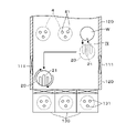
- FIG. 1 shows a multi-chamber type wafer processing system 100 having a plurality of wafer processing chambers 110 which are substrate processing chambers for processing wafers W.
- the wafer processing system 100 includes a load port 141 , an atmospheric transfer chamber 140 , a load lock chamber 130 , a vacuum transfer chamber 120 and a plurality of wafer processing chambers 110 .
- the direction in which the load port 141 is provided as viewed from the vacuum transfer chamber 120 is the front side.
- the load port 141, the atmospheric transfer chamber 140, the load lock chamber 130, and the vacuum transfer chamber 120 are horizontally arranged in this order from the front side.
- a plurality of wafer processing chambers 110 are arranged side by side on the left and right sides of the vacuum transfer chamber 120 as viewed from the front side.
- the load port 141 is configured as a mounting table on which a carrier C containing a wafer W to be processed is mounted, and four load ports 141 are arranged side by side in the horizontal direction when viewed from the front side.
- a carrier C for example, a FOUP (Front Opening Unified Pod) or the like can be used.
- the atmospheric transfer chamber 140 has an atmospheric pressure (normal pressure) atmosphere, and for example, clean air downflow is formed.
- a wafer transfer mechanism 142 for transferring the wafer W is provided inside the atmosphere transfer chamber 140 .
- a wafer transfer mechanism 142 in the atmosphere transfer chamber 140 transfers the wafer W between the carrier C and the load lock chamber 130 .
- An alignment chamber 150 for alignment of the wafer W is provided, for example, on the left side of the atmospheric transfer chamber 140 .
- the load lock chamber 130 has lifting pins 131 that push up and hold the loaded wafer W from below. Three elevating pins 131 are provided at regular intervals in the circumferential direction and configured to be movable up and down.
- the load lock chamber 130 is configured to switch between an atmospheric pressure atmosphere and a vacuum atmosphere.
- the load lock chamber 130 and the atmosphere transfer chamber 140 are connected via a gate valve 133 .
- the load lock chamber 130 and the vacuum transfer chamber 120 are connected via a gate valve 132 .
- a boundary portion between the vacuum transfer chamber 120 and the load lock chamber 130 is connected so as not to form a step on the floor surface.
- the vacuum transfer chamber 120 is evacuated to a vacuum atmosphere by a vacuum exhaust mechanism (not shown).
- the vacuum transfer chamber 120 corresponds to the substrate transfer chamber of this embodiment.
- the vacuum transfer chamber 120 in which the wafers W are transferred in a vacuum atmosphere is composed of a rectangular casing elongated in the front-rear direction when viewed from above.
- three wafer processing chambers 110 in total ie, six wafer processing chambers 110 in total, are provided via gate valves 111 on the right and left side walls of the vacuum transfer chamber 120 .
- a wafer W is carried in and out between the vacuum transfer chamber 120 and the wafer processing chamber 110 through an opening (not shown) that is opened and closed by the gate valve 111 .
- Each wafer processing chamber 110 is connected to the vacuum transfer chamber 120 through the above-mentioned opening provided with the gate valve 111 .
- a mounting table 112 is provided inside each wafer processing chamber 110 .
- a predetermined process is performed on the wafer W mounted on the mounting table 112 while the pressure is reduced to a vacuum atmosphere by a vacuum exhaust mechanism (not shown). Examples of the processing to be performed on the wafer W include etching processing, film formation processing, cleaning processing, ashing processing, and the like.
- the mounting table 112 is provided with, for example, a heater (not shown) for heating the wafer W to a predetermined temperature.
- the wafer processing chamber 110 is provided with a processing gas supply unit (not shown) constituted by a shower head or the like.
- the wafer processing chamber 110 corresponds to the substrate processing chamber of this embodiment.
- the wafer processing chambers 110 are installed so as to face each other with each area sandwiched from the left and right. ing.
- a wafer transfer arm 5, which is a substrate transfer mechanism, is provided in each of the front region and the middle region.
- the wafer transfer arm 5 includes a base 50 fixed to the bottom surface of the vacuum transfer chamber 120 and a lower arm portion connected above the base 50 via a rotation shaft (not shown). 51, an upper arm portion 52, and a wafer holding portion 53 arranged in two stages are connected in this order from the lower side to form a joint arm.
- the wafer transfer arm 5 can extend and retract and rotate about the vertical axis.
- the wafer transfer arm 5 provided in the front region (front side) and the wafer transfer arm 5 provided in the middle region (rear side) are indicated by A and B, respectively (5A, 5B).
- the mounting portion 4 is provided with three elevating pins 41 for supporting the wafer W so as to form a triangular support surface.
- the elevating pins 41 are configured to protrude from the bottom surface of the vacuum transfer chamber 120 by an elevating mechanism (not shown) to push up and hold the wafer W from below.
- a region where the wafer W supported by the elevating pins 41 is projected onto the bottom surface of the vacuum transfer chamber 120 is indicated as the mounting portion 4 by a dashed line.
- the placement section 4 arranged between the wafer transfer arm 5A and the wafer transfer arm 5B and the placement section 4 provided on the back side of the wafer transfer arm 5B are indicated with reference numerals A and B, respectively (4A and 4B). .
- Mounting units 4A and 4B are configured such that lift pins 41 protrude from the bottom surface of vacuum transfer chamber 120 when wafer W is held. It descends below the bottom surface of 120 . Accordingly, when the wafer W is not held, first and second transfer modules 20 and 30, which will be described later, can pass above the mounting sections 4A and 4B.
- the distance in the front-rear direction between the mounting portions 4A, 4B and the bases 50 of the wafer transfer arms 5A, 5B is determined by a first transfer module, which will be described later, even when the lifting pins 41 are raised. 20 can pass through (Fig. 2).
- the distance between the base 50 of the wafer transfer arm 5A on the front side and the load lock chamber 130 in the front-rear direction is also set to a distance that allows the first transfer module 20 to pass under the same conditions.
- the space in the front-rear direction between the mounting portion 4B on the far side and the wall surface on the far side of the vacuum transfer chamber 120 is such that the second transfer module 30, which will be described later, takes a posture in which the arm portion 32 faces the front-rear direction. It is set at an interval that can be
- the wafer transfer arm 5 (5A, 5B) is arranged in the vacuum transfer chamber 120 so as to be sandwiched between two openings to which the wafer processing chamber 110 is connected.
- the layout is such that a plurality of mounting sections 4 are arranged along the alignment of these openings and the wafer transfer arm 5 .
- first and second transfer modules 20 and 30, which are substrate transfer modules for transferring wafer W, are housed in addition to wafer transfer arms 5A and 5B.
- a disk-shaped first transfer module 20 and a second transfer module 30 having an arm portion 32 having a fork-shaped substrate holding portion are accommodated.
- the first and second transfer modules 20 are configured to be movable within the vacuum transfer chamber 120 by magnetic levitation. In the following, the configuration of equipment related to the transfer and processing of the wafer W using the transfer module 20 will be described in detail.
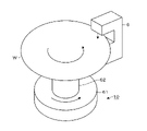
- the first transfer module 20 includes a stage 2 which is a substrate holder on which a wafer W is placed and held.
- the stage 2 is formed in the shape of a flat disk, and its upper surface serves as a mounting surface for mounting a wafer W to be transferred and processed.
- the first transfer module 20 has a mounting portion 4A, 4B and the lift pins 41, 131 in the load lock chamber 130 so as not to interfere with each other.
- Three slits 21 are formed extending along the length of the groove.
- directing the opening end side of the slit 21 in a predetermined direction may be expressed as facing the first transfer module 20.
- the relationship between the elevating pins 41 and 131 and the slit 21 will be explained using the mounting section 4 in the vacuum transfer chamber 120 as an example.
- the lifting pin 41 is in a state of protruding from the floor surface.
- the first transfer module 20 is placed on the front side of the mounting section 4 and moved toward the back side of the vacuum transfer chamber 120 in a posture facing the back side of the vacuum transfer chamber 120 .
- a space is secured between the mounting portion 4 and the base 50 of each wafer transfer arm 5 so that the first transfer module 20 can pass therethrough. Therefore, the first transfer module 20 can be arranged at a position directly facing the mounting section 4 without interference between the first transfer module 20 and the lifting pin 41 .
- the first transfer module 20 is placed on the rear side of the mounting section 4 and moved toward the front side in a posture facing the front side of the vacuum transfer chamber 120 .
- the forming area of the slit 21 is moved along the arrangement position of the lifting pin 41 .
- the first transfer module 20 and the mounting section 4 can be arranged vertically so that the centers of the first transfer module 20 and the lifting pins 41 are aligned without interfering with each other.
- a plurality of floor-side coils 15 are arranged in the floor portions 10 of the vacuum transfer chamber 120 and the load lock chamber 130, respectively.
- the floor-side coil 15 generates a magnetic field when power is supplied from a power supply unit (not shown). From this point of view, the floor-side coil 15 corresponds to the first magnet of the present embodiment.
- a plurality of module-side coils 35 are also arranged inside the first transfer module 20 .
- a repulsive force acts between the module-side coil 35 and the magnetic field generated by the floor-side coil 15 .
- the first transfer module 20 can be magnetically levitated with respect to the floor section 10 .
- the first transfer module 20 can be moved in a desired direction on the floor unit 10, the floating amount can be adjusted, and the first Adjustments to the orientation of the transport module 20 can be made.
- the module-side coil 35 provided in the first transfer module 20 corresponds to the second magnet in this embodiment. Power is supplied to the module-side coil 35 from a battery (not shown), which is a magnet power supply unit provided in the first transfer module 20, and functions as an electromagnet.
- a configuration may be adopted in which a permanent magnet is provided as an auxiliary inside the first transfer module 20 .
- the module-side coil 35 may be composed only of permanent magnets.
- each module-side coil 35 is controlled by a power supply control unit (not shown) provided in the first transfer module 20 to increase/decrease power supplied to the module-side coil 35 and to control supply/stop.
- the power supply control unit may be configured to obtain a control signal related to power supply control through wireless communication with the control unit 9, which will be described later.
- the first transfer module 20 is formed to have dimensions that enable it to pass between the bases 50 of the wafer transfer arms 5A and 5B and the mounting section 4 (FIGS. 1 and 2).
- the second transfer module 30 is formed to have a height dimension that allows it to pass below the swiveling lower arm portion 51 of the wafer transfer arms 5A and 5B while holding the wafer W. .
- the second transfer module 30 has substantially the same width dimension as the first transfer module 20 and includes a main body 31 having a rectangular plane shape.
- the body portion 31 is provided with an arm portion 32 which extends horizontally and holds the wafer W horizontally.
- a fork that can be arranged so as to surround the area where the three lifting pins 41 and 131 are provided is provided at the tip of the arm portion 32 .
- the fork corresponds to the substrate holder in the second transfer module 30 .
- the arm portion 32 receives the wafer W on the mounting table 112 by opening the gate valve 111 and inserting the arm portion 32 into the wafer processing chamber 110 while the body portion 31 is positioned inside the vacuum transfer chamber 120 . It is set to a length that can be passed.
- a module-side coil 35 similar to that of the first transfer module 20 is provided inside the body portion 31 of the second transfer module 30 .
- the second transfer module 30 can be moved in a desired direction on the floor surface 10, the floating amount can be adjusted, and the direction of the second transfer module 30 can be adjusted. It can be performed.
- the vacuum transfer chamber 120 which includes the first and second transfer modules 20 and 30 and the wafer transfer arm 5 described above and is connected to the wafer processing chamber 110, constitutes the substrate transfer apparatus of the present disclosure. ing.
- the wafer processing system 100 having the configuration described above includes a controller 9 that controls the floor-side coils 15, the wafer processing chamber 110, and the like.
- the control unit 9 is composed of a computer having a CPU and a storage unit, and controls each unit of the wafer processing system 100 .
- the storage unit stores a program in which a group of steps (instructions) for controlling the operations of the first and second transfer modules 20 and 30 and the wafer processing chamber 110 are assembled. This program is stored in a storage medium such as a hard disk, compact disc, magnetic optical disc, memory card, etc., and is installed in the computer from there.
- the wafer processing system 100 First, when the carrier C accommodating the wafers W to be processed is placed on the load port 141 , the wafers W are taken out from the carrier C by the wafer transfer mechanism 142 in the atmosphere transfer chamber 140 . The wafer W is then transferred to the alignment chamber 150 and aligned. Further, when the wafer W is taken out from the alignment chamber 150 by the wafer transfer mechanism 142, the gate valve 133 is opened.
- the wafer transfer mechanism 142 enters the load lock chamber 130, and the lifting pins 131 push up the wafer W and receive it.
- the first wafer W is loaded into the leftmost load lock chamber 130 when viewed from the front side to the back side.
- the gate valve 133 is closed.
- the inside of the load lock chamber 130 is switched from the atmospheric pressure atmosphere to the vacuum atmosphere.
- the wafer W is similarly transferred to each load lock chamber 130.
- the second wafer W is transferred to the rightmost load lock chamber 130, for example.
- the gate valve 132 When the inside of the load lock chamber 130 becomes a vacuum atmosphere, the gate valve 132 is opened. At this time, in the vacuum transfer chamber 120 , the first transfer module 20 ⁇ /b>A stands by in the vicinity of the connection position of the load lock chamber 130 in a posture facing the load lock chamber 130 .
- the magnetic field generated by the floor-side coil 15 provided on the floor unit 10 is used to raise the first transfer module 20A by magnetic levitation using a repulsive force.
- the first transfer module 20A is moved into the load lock chamber 130 and positioned below the wafer W supported by the lifting pins 131. Then, as shown in FIG. The wafer W is mounted on the stage 2 by further lowering the lifting pins 131 and transferring the wafer W to the first transfer module 20 .
- the first transfer module 20A holding the wafer W is withdrawn from the load lock chamber 130 and is moved straight to the front side of the receiver A4. Subsequently, the first transfer module 20A moves rightward between the mounting section 4A on the front side and the base 50 of the wafer transfer arm 5A on the front side. At this time, the first transfer module 20A translates rightward without changing its direction. Then, after moving to the front of the rightmost placement section 4A, the movement direction is changed to the rear side and the upper portion of the placement section 4 is reached (FIG. 8).
- the elevating pins 41 are raised to push up and receive the wafer W held by the first transfer module 20A.
- the subsequent wafer W is loaded into the leftmost load-lock chamber 130, and the atmosphere in the load-lock chamber 130 is similarly switched to a vacuum atmosphere.
- the first transfer module 20B enters the load lock chamber 130 and receives the wafer W therefrom.
- the first transfer module 20A that has delivered the wafer W moves to the back side of the mounting section 4A, and moves the back side of the front side mounting section 4A from the right side to the left side. . Further, the first transfer module 20A goes straight toward the near side and waits on the far side of the load lock chamber 130 on the left side. Note that the first transfer module 20A is moved to the placement section 4A in a state in which the lifting pins 41 are not lifted while maintaining the posture facing the load lock chamber 130. As shown in FIG. Therefore, the first transfer module 20A can move along the trajectory shown in FIG. 9 without interfering with the lifting pins 41. This point is the same for the operation of the other first transfer module 20B.
- the front wafer transfer arm 5A receives the wafer W transferred to the right mounting portion 4A, and transfers the wafer W to the front right wafer processing chamber 110, for example.
- the first transfer module 20B holding the succeeding wafer W leaves the load lock chamber 130 and advances straight to the front of the mounting section 4A.
- the direction of movement is changed to move to the left between the mounting portion 4A and the wafer transfer arm 5A on the front side.
- the moving direction is changed to the rear side and reaches the upper side of the mounting portion 4A (FIG. 9).
- the elevating pins 41 of the mounting portion 4A are lifted, and the wafer W is transferred to the elevating pins 41. As shown in FIG.
- the first transfer module 20B that has delivered the wafer W moves to the far side of the mounting section 4, and then changes its moving direction to the right. After that, it goes straight toward the near side and waits on the far side of the rightmost load lock chamber 130 .
- the back side wafer transfer arm 5B receives the wafer W transferred to the central mounting portion 4A, and transfers the wafer W to, for example, the right wafer processing chamber 110 in the middle.
- FIG. 11 the case of transfer to the wafer processing chamber 110 installed on the right side of the rear stage of the vacuum transfer chamber 120 will be described.
- the wafer W is transferred to the first transfer module 20 in, for example, the left load lock chamber 130 .
- the first transfer module 20 that has received the wafer W moves straight toward the rear side to the front side of the mounting section 4B on the rear side.
- the first transfer module 20 changes its movement direction and moves to the right between the mounting section 4B on the far side and the wafer transfer arm 5B on the far side. Then, after moving to the front of the right mounting portion 4B, the moving direction is changed to the back side and reaches above the right mounting portion 4B. Then, for example, it rotates around the vertical axis on the spot, and changes its direction so as to face the placing section 4B.
- the first transfer module 20 faces the front side when coming out of the load lock chamber 130, if it is rotated 180° around the vertical axis above the mounting section 4, good.
- the second transfer module 30 is on standby with the arm portion 32 facing forward on the far side of the right mounting portion 4B.
- the first transfer module 20 moves forward. Further, after rotating 180° about the vertical axis, the first transfer module 20 moves leftward between the rear side mounting portion 4B and the rear side wafer transfer arm 5B. Further, it goes straight to the near side and returns to the far side of the leftmost load lock chamber 130 to wait. On the other hand, the second transfer module 30 is moved forward to position the arm portion 32 on the mounting portion 4B, and the lifting pins 41 of the mounting portion 4B are lowered to transfer the wafer W to the arm portion 32. .
- the second transfer module 30 holding the wafer W is reversed to move backward while changing its direction when viewed from the mounting section 4B, and the tip of the arm section 32 is moved to the wafer processing chamber on the right side.
- the gate valve 111 of the wafer processing chamber 110 is opened, the second transfer module 30 is moved straight, and the arm portion 32 enters the wafer processing chamber 110 to transfer the wafer W thereon.
- the body portion 31 of the second transfer module 30 is positioned inside the vacuum transfer chamber 120, and only the arm portion 32 enters the wafer processing chamber 110 (FIG. 13).
- the wafer transfer arms 5A and 5B and the arm section 32 are retracted to the vacuum transfer chamber 120, and the gate valve 111 is closed. Subsequently, the wafer W is sequentially heated by the mounting table 112 to raise the temperature to a preset temperature, and a processing gas is supplied from the processing gas supply unit into the wafer processing chamber 110 . Thus, the desired processing for wafer W is performed.
- the heating of the wafer W is stopped and the supply of the processing gas is stopped.
- the wafer W may be cooled by supplying a cooling gas into the wafer processing chamber 110 as necessary.
- the wafer W is transported in the reverse order of the carrying-in procedure, and the wafer W is returned from the wafer processing chamber 110 to the load lock chamber 130 .
- the atmosphere of the load lock chamber 130 is switched to the normal pressure atmosphere, the wafer W in the load lock chamber 130 is taken out by the wafer transfer mechanism 142 on the atmospheric transfer chamber 140 side and returned to the predetermined carrier C.
- the first transfer module 20 transfers from the load lock chamber 130 to the mounting section 4 provided in the vacuum transfer chamber 120 .
- the first transfer module 20 is not provided in the vacuum transfer chamber 120, there is a space between the load lock chamber 130 and the front stage mounting section 4A and the rear stage mounting section 4A and the rear stage mounting section 4A. It is also necessary to use the wafer transfer arms 5A and 5B to transfer the wafer W to and from the mounting portion 4B in the front-rear direction.
- each wafer transfer arm 5A, 5B is added to the operation of transferring the wafer W in the front-rear direction in addition to the operation of transferring the wafer W to the wafer processing chamber 110 .
- the load of the operation of transferring the wafer W by the wafer transfer arms 5A and 5B increases.
- An increase in the load on a specific device may restrict the increase in the number of wafers W that can be processed per unit time by the wafer processing system 100 .
- the addition of a dedicated wafer transfer arm for transferring the wafer W in the front-rear direction causes problems such as lack of arrangement space, interference with the other wafer transfer arms 5A and 5B, and transfer of the wafer by the additional wafer transfer arm. It is not realistic due to restrictions on possible positions.
- the transfer of the wafer W from the load lock chamber 130 to each mounting section 4 can be performed in the first mode.
- the transport module 20 can be shared by the transport module 20 . Therefore, the wafer transfer arm 5 only has to share the transfer of the wafer W between the mounting section 4 and the wafer processing chamber 110 . Therefore, an increase in the load on the wafer transfer arm 5 can be suppressed.
- a plurality of mounting units 4 are arranged along the alignment of the wafer processing chamber 110 and the wafer transfer arm 5 . With this configuration, the transfer operation of the wafer W by the wafer transfer arm 5 and the first transfer module 20 can be efficiently performed while securing the movement space of the first transfer module 20 .
- the floor side coil 15 may also be installed on the floor of the wafer processing chamber 110 so that the first transfer module 20 can directly enter the wafer processing chamber 110 to transfer the wafer W.
- the first and second transfer modules 20 and 30 having different usable temperatures may be used depending on the temperature of the wafer W before and after processing in the wafer processing chamber 110 .
- the wafer W when the wafer W is transferred by the first transfer module 20, alignment of the notch and the orientation flat (OF) of the wafer W may be performed.
- the wafer processing chambers 110 when the wafer processing chambers 110 are arranged on both sides of the wafer transfer arm 5, the wafers W mounted on the mounting portion 4 are always oriented in the same direction. In this case, the notches and OF directions may differ by 180° between the left and right wafer processing chambers 110 .
- the first transfer module 20 can also be used for notch and OF alignment. 14 and 15 described below, the illustration of the wafer transfer arm 5 is omitted for convenience of illustration.
- notch alignment Assume that wafers W whose notches have been aligned by alignment are arranged as shown in FIG. 14 .
- the wafer W is placed on the placement unit 4 without changing the direction of the notch, and the wafer W is carried into the wafer processing chamber 110 on the right side by the wafer transfer arm 5, the wafer W is moved to the preset direction. , the wafer W is rotated by 180° around the vertical axis.
- the first transfer module 20 holding the wafer W enters the vacuum transfer chamber 120 from the load lock chamber 130
- the first transfer module 20 is rotated around the vertical axis as shown in FIG. Rotate 180°.
- the direction of the wafer W to be transferred to the mounting section 4 can be rotated by 180°.
- the first transfer module 20 is withdrawn from the position of the mounting section 4, rotated 180° around the vertical axis, and returned to the far side of the leftmost load lock chamber 130 to wait (FIG. 16).
- FIGS. 17 and 18 show an example of a mounting module 400 constituting a substrate transfer section arranged on the mounting section 4.
- FIG. This mounting module 400 is configured to be rotatable about a vertical axis using magnetic levitation.
- the mounting module 400 has two mounting tables 401 and 402 so that the wafer W can be mounted on two stages, one above the other.
- the mounting table 401 on the lower side has a table portion 411 , and a holding portion 403 for holding the center of the lower surface of the wafer W is provided above the table portion 411 .
- the holding section 403 is configured to transfer the wafer W to and from the wafer holding section 53 of each first transfer module 20 .
- the upper mounting table 402 has a cylindrical portion 412 surrounding the lower mounting table 401 , and a holding portion 404 for holding the center of the lower surface of the wafer W is provided above the cylindrical portion 412 .
- Two window portions 405 for transferring the wafer W to the mounting table 401 on the lower stage side are formed at positions facing each other on the side surface of the cylindrical portion 412 .
- the holding section 404 is also configured to transfer the wafer W to and from the wafer holding section 53 of each first transfer module 20 .
- Module-side coils 35 which are magnets on the substrate transfer section side, are provided at the lower ends of the base portion 411 of the mounting table 401 and the cylindrical portion 412 of the mounting table 402, respectively.
- the mounting tables 401 and 402 rotate independently around the vertical axis. freely configured.
- the orientation of the wafer W can be changed between when it is held by the first transfer module 20 and when it is held by the wafer transfer arm 5 .
- the notch and OF positioning operations of the wafer W by the first transfer module 20 described with reference to FIGS. can share the transport and rotation of the
- FIG. 19 shows an example of alignment of the wafer W using a transfer module using magnetic levitation.
- a transfer module 60 illustrated in FIG. 19 includes a body portion 61 provided with a module-side coil 35 and a column portion 62 that extends upward from the upper surface of the body portion 61 and has a diameter smaller than that of the wafer W. I have.
- a substrate holding surface forming a substrate holding portion is formed on the upper surface of the column portion 62, and the wafer W is supported from the lower surface side by the substrate holding surface.
- the wafer sensor 6 for alignment is used, which is a detection unit having a light receiving unit that emits light downward and receives the light from the lower side.
- the wafer sensor 6 detects the position of the peripheral edge of the wafer W located outside the column portion 62 .
- the wafer sensor 6 is provided in the load lock chamber 130, for example.
- the wafer W is transferred from the atmospheric transfer chamber 140 side to the transfer module 60, and the gate valve 133 on the atmospheric transfer chamber 140 side is closed. Further, the transfer module 60 is moved so that the peripheral edge of the wafer W is positioned on the optical path of the wafer sensor 6 .
- the transfer module 60 is rotated around the vertical axis on the spot.
- the wafer W rotates around the central axis passing through its center, and alignment is performed while the position of the peripheral edge of the rotating wafer W is detected.
- the installation of the alignment chamber 150 shown in FIG. 1 can be omitted, and the size of the wafer processing system 100 can be reduced.
- the number of wafers W processed per unit time can be improved compared to, for example, an example in which alignment is performed by transferring the wafers W to the alignment chamber 150 . be able to.
- the sensor unit 6 may be provided in the movement area of the transfer module 60 such as the atmosphere transfer chamber 140 or the vacuum transfer chamber 120, and the alignment may be performed at each installation location.
- the above-described transfer module 60 also corresponds to the substrate transfer module of this example, and instead of or together with the above-described first and second transfer modules 20 and 30, the wafer W can be transferred within the vacuum transfer chamber 120. may be executed.
- the raising/lowering pins 41 of the mounting portion 4 are arranged at a position capable of supporting the lower surface of the wafer W around the supporting column portion 62 .
- each of the transfer modules 20, 30, and 60 described above may be provided with an accelerometer or a thermometer to detect the vibration of the wafer W during transfer or detect the temperature rise of the wafer W. Measured values of acceleration and temperature, for example, are transmitted to the control unit 9, and failure of the transfer modules 20, 30, and 60 is detected when, for example, the measured acceleration value exceeds a threshold value or the measured temperature value exceeds a threshold value. Self-diagnosis may be performed. Further, an abnormality in the wafer W processing process may be detected when the measured value of the temperature of the wafer W exceeds a threshold value.
- a camera for monitoring the inside of the vacuum transfer chamber 120 may be provided in the disk-shaped first transfer module 20 .
- the first transfer module 20 may be moved into the wafer processing chamber 110 and an image of the interior of the chamber may be taken to check for an abnormality.
- the wafer W mounted on the mounting table 112 and the mounting table 112 are imaged, and the position of the wafer W and the position of the mounting table 112 are confirmed, thereby confirming the accuracy of the teaching and transfer of the wafer W.
- a laser displacement meter or encoder may be installed to further improve the accuracy of position confirmation.
- an imaging module that can move in the vacuum transfer chamber 120 by magnetic levitation may be provided, and a camera may be installed in the imaging module.
- a magnet is provided on the ceiling (top surface portion) side of the substrate transfer chamber (for example, the vacuum transfer chamber 120 described above) in which the wafer W is transferred, and the wafer W is moved along the ceiling by magnet attraction.
- the example which provided the module is shown.
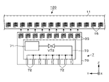
- a gas discharge module 7 will be described as an example of such a module.
- the gas discharge module 7 has a housing 70.
- a gas reservoir 71 in which, for example, nitrogen (N 2 ) gas, which is a clean gas, is reserved.
- a plurality of gas discharge holes 72 are formed in the lower surface of the housing 70, and the N2 gas stored in the gas reservoir 71 is discharged from the gas discharge holes 72 via a pipe 73. It is Note that V73 provided in the pipe 73 in FIG. 20 is a valve.
- the module-side coil 35 is provided on the top plate of the housing 70 , and the top-surface portion-side coil 16 is installed on the top surface portion 11 of the vacuum transfer chamber 120 .
- the top surface side coil 16 corresponds to a third magnet
- the module side coil 35 corresponds to a fourth magnet.
- the module-side coil 35 and the top-panel-side coil 16 magnetically attract the gas discharge module 7 below the top panel 11 in the vacuum transfer chamber 120 by magnetic attraction.
- the gas discharge module 7 configured as described above discharges N2 gas while moving, for example, in the vacuum transfer chamber 120 as shown in FIG. As a result, a downward flow of clean gas is formed toward the wafer W in the vacuum transfer chamber 120 .
- This downward flow suppresses adhesion of particles 93 drifting in the vacuum transfer chamber 120 and corrosive gas 94 generated during processing in the wafer processing chamber 110 to the wafer W, and the flow of the N 2 gas suppresses the adhesion of the corrosive gas 94 to the wafer W.
- the gas discharge module 7 follows the transfer modules 20 and 30 so as to continue discharging the N2 gas onto the wafer W held by the transfer modules 20 and 30. You can move it by moving it. With this configuration, the wafer W being transported can be covered with the N2 gas, and the wafer W can be prevented from being oxidized by the gas floating in the transport path.
- a temperature control module that houses a heater or the like may be used as the module that is provided on the top surface side and moves. For example, by moving a temperature control module arranged above the wafer W together with the wafer W transported by the first transport module 20 that moves along the floor surface, the wafer W is transported while the wafer W is being transported. Temperature can be adjusted.
- a module that moves along the ceiling may be provided with a shelf-like wafer mounting portion, and the wafer W may be transported using the module.
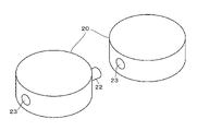
- FIG. 22 shows an example in which a protrusion 22 is provided on the side surface of the first transfer module 20.
- a recess 23 into which the protrusion 22 can be inserted is provided on the side surface opposite to the protrusion 22 .
- the projecting portion 22 of the first transfer module 20 is inserted into the concave portion of the other first transfer module 20 so as to be connected.
- the projecting portion 22 and the recessed portion 23 constitute a connecting mechanism.
- the failed first transport module 20 when the first transport module 20 fails and becomes immovable, the failed first transport module 20 is connected by another first transport module 20 so as to sandwich the failed first transport module 20 .
- the hatched first transfer module 20 in FIG. 23 indicates the failed first transfer module 20 .
- the failed first transport module 20 can be transported by another first transport module 20 .
- a dedicated load lock chamber 200 may be provided in which the internal atmosphere can be switched between an air atmosphere and a vacuum atmosphere in order to carry out the failed first transfer module 20 .
- FIG. 24 shows an example in which the load lock chamber 200 is provided on the rear side wall surface of the vacuum transfer chamber 120 .
- Reference numeral 201 in FIG. 24 denotes a gate valve, and reference numeral 202 denotes an outlet of the first transfer module 20.
- the wafer processing system 100 does not need to be stopped and opened, and downtime of the system 100 can be reduced. Further, from the load lock chamber 200, the wafer W in which an abnormality has occurred may be recovered.
- the load-lock chamber 200 described above may be used as a storage chamber for storing unused transfer modules 20, 30, and 60.
- the number of transfer modules 20 , 30 , 60 used in the vacuum transfer chamber 120 may be adjusted according to the throughput of the processing performed in the wafer processing system 100 .
- the number of transfer modules 20 , 30 , 60 arranged in the vacuum transfer chamber 120 via the load lock chamber 200 may be increased or decreased.
- the transfer modules 20, 30, and 60 may be used to transfer components installed in the vacuum transfer chamber 120 or the wafer processing chamber 110.
- FIG. 25 shows an example of carrying the focus ring 113 by the first carrying module 20 .
- the wafer transfer arm 5 may receive the focus ring 113 from the first transfer module 20 , carry it into the wafer processing chamber 110 , and set it on the mounting table 112 . With this configuration, it is possible to replace and install internal parts and members without opening the wafer processing chamber 110 .
- the first transfer module 20 may be configured to have a rectangular planar shape.
- the transfer module 20 having a circular planar shape the area required for rotation of the transfer module 20 can be reduced, and the area of the vacuum transfer chamber 120 can be reduced.
- the transfer of the wafer W between the first transfer module 20 and the wafer transfer arm 5 may be performed directly between the first transfer module 20 and the wafer transfer arm 5 without going through the mounting section 4. good.
- elevating pins projecting from the surface of the stage 2 of the first transfer module 20, for example, are provided. Then, the wafer W placed on the first transfer module 20 may be lifted and transferred to and from the wafer transfer arm 5 using the lifting pins.
- the number and layout of the wafer processing chambers 110 in the vacuum transfer chamber 120 are not limited to the example shown in FIG.
- the number of wafer processing chambers 110 arranged may be increased or decreased as required.
- providing only one wafer processing chamber 110 in the vacuum transfer chamber 120 is also included in the technical scope of the present disclosure.
- the arrangement of the vacuum transfer chamber 120 is not limited to the case where the long sides of the vacuum transfer chamber 120 having a rectangular planar shape are directed in the front-rear direction as shown in FIG.
- the vacuum transfer chamber 120 when viewed from the load port 141 side, the vacuum transfer chamber 120 may be arranged such that the long side is oriented in the horizontal direction.
- the planar shape of the vacuum transfer chamber 120 may also have various shapes depending on the shape of the area in which the wafer processing system 100 is arranged. For example, it may be a square, a polygon with pentagons or more, a circle, or an ellipse.
- the substrate transfer chamber in which the wafer W is transferred to the wafer processing chamber 110 using the transfer modules 20, 30, and 60 is not limited to the vacuum transfer chamber 120 having a vacuum atmosphere inside.
- the transfer modules 20, 30, and 60 of the present disclosure can also be applied to a wafer processing system in which the wafer processing chamber 110 is provided on the side of the substrate transfer chamber whose interior is in an atmospheric pressure atmosphere. In this case, provision of the load lock chamber 130 for the wafer processing system is not an essential requirement, and the wafer W taken out from the carrier C into the atmospheric transfer chamber 140 may be directly transferred into the substrate transfer chamber. .
- the vacuum transfer chamber 120A and another vacuum transfer chamber 120B may be connected by the communication path 8.
- one end of communication path 8 is connected to the left side of vacuum transfer chamber 120A, and the other end of communication path 8 is connected to the right side of another vacuum transfer chamber 120B.
- the vacuum transfer chamber 120B has the same configuration as the vacuum transfer chamber 120A except that the load lock chamber 130 is not provided on the front side.
- a floor-side coil 15 is also installed on the floor of the connecting path 8, and the transfer modules 20, 30, and 60 are configured to be movable.
- the load lock chamber 130, atmospheric transfer chamber 140 and load port 141 can be shared.
- the wafer transfer arm 5 for example, is used as the wafer transfer mechanism that fixes the space between the vacuum transfer chambers 120A and 120B to the bottom surface, a large space for turning is required.
- a plurality of conveying mechanisms must be provided in order to convey to a distant point.
- the range in which the floor-side coil 15 can be installed can be adjusted relatively freely.
- the range in which one transfer module 20, 30, 60 can move can be freely set, so that the degree of freedom in device design increases.
- FIG. 27 shows a wafer processing system 101 that transfers a wafer W using only the second transfer module 30 (hereinafter also simply referred to as "transfer module 30").
- transfer module 30 the second transfer module 30
- the length in the short side direction of the rectangular vacuum transfer chamber 160 in plan view is such that the two transfer modules 30 each holding a wafer W pass each other in a state of being laterally aligned. It is as wide as possible.
- the length of the short side direction of the vacuum transfer chamber 160 in this example is the length from the main body 31 to the tip of the wafer W when the transfer module 30 holds the wafer W (the transfer module in the state of holding the wafer W). 30 total length).
- the wafer W is transferred using two transfer modules 30 provided in the vacuum transfer chamber 160 .
- Two load lock chambers 130 are arranged side by side on the front side of the vacuum transfer chamber 160 , and four wafer processing chambers 110 are arranged on each side of the vacuum transfer chamber 160 . That is, the wafer W is loaded into the wafer processing chamber 110 in a direction (short side direction) crossing the long side direction of the vacuum transfer chamber 160 .
- the length in the short side direction of the vacuum transfer chamber 160 is shorter than the total length of the transfer module 30 holding the wafer W thereon. Therefore, when the transfer module 30 is used to load and unload the wafer W, the wafer W is transferred to the vacuum transfer chamber 160 while moving linearly along the long side direction of the vacuum transfer chamber 160 and changing the orientation of the transfer module 30 . It is necessary to perform a turning motion combined with a curvilinear movement entering or exiting the vehicle.
- a space 161 is provided on the rear side of the vacuum transfer chamber 160 for performing a switching operation when the transfer module 30 is switched when the wafer W is transferred into the final wafer processing chamber 110 . That is, the space 161 is provided so as to protrude farther than the rearmost wafer processing chamber 110 (specifically, the position of the gate valve 111 of the rearmost wafer processing chamber 110).
- the space in the vacuum transfer chamber 160 that is wider on the front side than the space 161 described above is used to perform the above-described switching operation. It can be carried out.
- the transfer module 30 moves along the long side direction of the vacuum transfer chamber 160 with the arm portion 32 directed toward the load lock chamber 130 (front side) in the vacuum transfer chamber 160. , moves on left and right trajectories as viewed from the front side.
- the transfer operation of the wafer W to and from the wafer processing chamber 110 in the wafer processing system 101 will be described by taking the last wafer processing chamber 110 on the left side as an example.
- the transfer module 30 receives the wafer W from the left load-lock chamber 130, it moves backward while keeping the arm portion 32 facing the front side (left hand side as viewed from the front side in FIG. 27). (see also the arrow indicating the direction of travel written together with the transport module 30 in ).
- the transfer module 30 holding the wafer W moves to the position where the gate valve 111 of the last wafer processing chamber 110 is provided.
- the body portion 31 of the transfer module 30 has passed the position where the gate valve 111 is arranged and has reached the space 161 on the far side.
- the tip side of the arm portion 32 holding the wafer W is arranged in the vicinity of the gate valve 111 . In this way, when the tip side of the arm portion 32 reaches the vicinity of the gate valve 111, as shown in FIG. .
- the gate valve 111 is opened, and the moving direction of the transfer module 30 is switched forward while rotating so as to insert the wafer W into the wafer processing chamber 110 (FIG. 29).
- the transfer module 30 faces the wafer processing chamber 110 , it stops rotating and moves straight until the wafer W reaches above the mounting table 112 .
- the transport module 30 assumes a posture in which the arm portion 32 faces leftward when viewed from the front side (FIG. 30).
- the wafer W is transferred to the mounting table 112 and the transfer module 30 is withdrawn from the wafer processing chamber 110 . Further, the gate valve 111 is closed and the wafer W is processed.
- transfer module 30 moves arm portion 32 into wafer processing chamber 110 again to receive processed wafer W.
- the transfer module 30 retracts the arm portion 32 not holding the wafer W from the wafer processing chamber 110 and moves it into the wafer processing chamber 110 as shown in FIGS. 28 to 33. Use the switchback operation described using .
- the back side of the vacuum transfer chamber 160 is provided with the space 161 for changing the direction while the transfer module 30 is switched.
- the width in the short side direction of the vacuum transfer chamber 160 can be made shorter than the total length of the transfer module 30 in a state where the wafer W is held. Therefore, the floor area of the vacuum transfer chamber 160 can be reduced.
- the space in the vacuum transfer chamber 160 that spreads on the front side of the space 161 is provided. can be used to perform a switching operation.
- this wafer processing system 101 does not include the wafer transfer arm 5 and the mounting section 4 in the vacuum transfer chamber 160, the height dimension of the vacuum transfer chamber 160 is reduced compared to the case where these devices 5 and 4 are provided. can be reduced.
Landscapes
- Container, Conveyance, Adherence, Positioning, Of Wafer (AREA)
- Engineering & Computer Science (AREA)
- Robotics (AREA)
- Non-Mechanical Conveyors (AREA)
Priority Applications (4)
| Application Number | Priority Date | Filing Date | Title |
|---|---|---|---|
| CN202280009603.0A CN116711059A (zh) | 2021-01-25 | 2022-01-12 | 进行基板的输送的装置、对基板进行处理的系统以及对基板进行处理的方法 |
| KR1020237027397A KR102834376B1 (ko) | 2021-01-25 | 2022-01-12 | 기판의 반송을 행하는 장치, 기판을 처리하는 시스템 및 기판을 처리하는 방법 |
| US18/273,446 US20240120225A1 (en) | 2021-01-25 | 2022-01-12 | Apparatus for transferring substrate, substrate processing system and method of processing substrate |
| KR1020257023157A KR20250112918A (ko) | 2021-01-25 | 2022-01-12 | 기판의 반송을 행하는 장치, 기판을 처리하는 시스템 및 기판을 처리하는 방법 |
Applications Claiming Priority (2)
| Application Number | Priority Date | Filing Date | Title |
|---|---|---|---|
| JP2021-009861 | 2021-01-25 | ||
| JP2021009861A JP7679629B2 (ja) | 2021-01-25 | 2021-01-25 | 基板の搬送を行う装置、基板を処理するシステム及び基板を処理する方法 |
Publications (1)
| Publication Number | Publication Date |
|---|---|
| WO2022158351A1 true WO2022158351A1 (ja) | 2022-07-28 |
Family
ID=82548928
Family Applications (1)
| Application Number | Title | Priority Date | Filing Date |
|---|---|---|---|
| PCT/JP2022/000747 Ceased WO2022158351A1 (ja) | 2021-01-25 | 2022-01-12 | 基板の搬送を行う装置、基板を処理するシステム及び基板を処理する方法 |
Country Status (6)
| Country | Link |
|---|---|
| US (1) | US20240120225A1 (https=) |
| JP (2) | JP7679629B2 (https=) |
| KR (2) | KR20250112918A (https=) |
| CN (1) | CN116711059A (https=) |
| TW (1) | TW202243089A (https=) |
| WO (1) | WO2022158351A1 (https=) |
Cited By (1)
| Publication number | Priority date | Publication date | Assignee | Title |
|---|---|---|---|---|
| US20230290656A1 (en) * | 2022-03-08 | 2023-09-14 | Tokyo Electron Limited | Apparatus for transferring member to be disposed in substrate processing chamber, substrate processing system, and method for transferring member |
Families Citing this family (4)
| Publication number | Priority date | Publication date | Assignee | Title |
|---|---|---|---|---|
| KR102662444B1 (ko) | 2023-07-21 | 2024-05-03 | 브이엠 주식회사 | 상하부 자기 부상 레일을 이용하는 기판 이송 장치 |
| WO2025057798A1 (ja) * | 2023-09-14 | 2025-03-20 | 東京エレクトロン株式会社 | 基板処理システム及び可動式メンテナンス装置 |
| JP2025085890A (ja) * | 2023-11-27 | 2025-06-06 | 東京エレクトロン株式会社 | 搬送モジュール、及び半導体製造装置における基板搬送方法 |
| JP2025187956A (ja) * | 2024-06-14 | 2025-12-25 | ヴイエム インコーポレイテッド | 基板移送装置 |
Citations (4)
| Publication number | Priority date | Publication date | Assignee | Title |
|---|---|---|---|---|
| JP2018504784A (ja) * | 2015-01-23 | 2018-02-15 | アプライド マテリアルズ インコーポレイテッドApplied Materials,Incorporated | 半導体処理設備 |
| JP2019509622A (ja) * | 2016-01-18 | 2019-04-04 | アプライド マテリアルズ インコーポレイテッドApplied Materials,Incorporated | 真空チャンバ内で基板キャリアを搬送するための装置、基板の真空処理のためのシステム、及び真空チャンバ内で基板キャリアを搬送するための方法 |
| JP2019518138A (ja) * | 2016-05-18 | 2019-06-27 | アプライド マテリアルズ インコーポレイテッドApplied Materials,Incorporated | 堆積源を搬送するための装置及び方法 |
| WO2019238416A1 (de) * | 2018-06-14 | 2019-12-19 | Robert Bosch Gmbh | Beförderungsvorrichtung zum befördern mindestens eines wafers |
Family Cites Families (13)
| Publication number | Priority date | Publication date | Assignee | Title |
|---|---|---|---|---|
| US5905850A (en) * | 1996-06-28 | 1999-05-18 | Lam Research Corporation | Method and apparatus for positioning substrates |
| JP3442253B2 (ja) * | 1997-03-13 | 2003-09-02 | 東京エレクトロン株式会社 | 基板処理装置 |
| JP2000299367A (ja) * | 1999-04-15 | 2000-10-24 | Tokyo Electron Ltd | 処理装置及び被処理体の搬送方法 |
| JP4330703B2 (ja) * | 1999-06-18 | 2009-09-16 | 東京エレクトロン株式会社 | 搬送モジュール及びクラスターシステム |
| JP4195227B2 (ja) * | 2002-02-22 | 2008-12-10 | 東京エレクトロン株式会社 | 被処理体の導入ポート構造 |
| US6896304B2 (en) * | 2002-09-03 | 2005-05-24 | Taiwan Semiconductor Manufacturing Co., Ltd. | Automatic sensing wafer blade and method for using |
| JP4665037B2 (ja) * | 2009-02-06 | 2011-04-06 | 東京エレクトロン株式会社 | 基板処理システム |
| IT1399285B1 (it) * | 2009-07-03 | 2013-04-11 | Applied Materials Inc | Sistema di lavorazione substrato |
| JP2011115021A (ja) * | 2009-11-30 | 2011-06-09 | Nikon Corp | 平面モータ装置及びステージ装置並びに露光装置 |
| CN101770180A (zh) * | 2010-02-02 | 2010-07-07 | 清华大学 | 一种采用多关节机械手的光刻机硅片台的线缆台 |
| JP6338989B2 (ja) * | 2014-09-19 | 2018-06-06 | 東京エレクトロン株式会社 | 基板搬送方法 |
| DE102014225171A1 (de) * | 2014-12-08 | 2016-06-09 | Robert Bosch Gmbh | Sicherungssystem für eine Anordnung zum Bewegen von Transportkörpern |
| US11527424B2 (en) * | 2020-03-20 | 2022-12-13 | Applied Materials, Inc. | Substrate transfer systems and methods of use thereof |
-
2021
- 2021-01-25 JP JP2021009861A patent/JP7679629B2/ja active Active
-
2022
- 2022-01-11 TW TW111101083A patent/TW202243089A/zh unknown
- 2022-01-12 KR KR1020257023157A patent/KR20250112918A/ko active Pending
- 2022-01-12 CN CN202280009603.0A patent/CN116711059A/zh active Pending
- 2022-01-12 US US18/273,446 patent/US20240120225A1/en active Pending
- 2022-01-12 KR KR1020237027397A patent/KR102834376B1/ko active Active
- 2022-01-12 WO PCT/JP2022/000747 patent/WO2022158351A1/ja not_active Ceased
-
2025
- 2025-05-08 JP JP2025078228A patent/JP2025111814A/ja active Pending
Patent Citations (4)
| Publication number | Priority date | Publication date | Assignee | Title |
|---|---|---|---|---|
| JP2018504784A (ja) * | 2015-01-23 | 2018-02-15 | アプライド マテリアルズ インコーポレイテッドApplied Materials,Incorporated | 半導体処理設備 |
| JP2019509622A (ja) * | 2016-01-18 | 2019-04-04 | アプライド マテリアルズ インコーポレイテッドApplied Materials,Incorporated | 真空チャンバ内で基板キャリアを搬送するための装置、基板の真空処理のためのシステム、及び真空チャンバ内で基板キャリアを搬送するための方法 |
| JP2019518138A (ja) * | 2016-05-18 | 2019-06-27 | アプライド マテリアルズ インコーポレイテッドApplied Materials,Incorporated | 堆積源を搬送するための装置及び方法 |
| WO2019238416A1 (de) * | 2018-06-14 | 2019-12-19 | Robert Bosch Gmbh | Beförderungsvorrichtung zum befördern mindestens eines wafers |
Cited By (2)
| Publication number | Priority date | Publication date | Assignee | Title |
|---|---|---|---|---|
| US20230290656A1 (en) * | 2022-03-08 | 2023-09-14 | Tokyo Electron Limited | Apparatus for transferring member to be disposed in substrate processing chamber, substrate processing system, and method for transferring member |
| US12512344B2 (en) * | 2022-03-08 | 2025-12-30 | Tokyo Electron Limited | Apparatus for transferring member to be disposed in substrate processing chamber, substrate processing system, and method for transferring member |
Also Published As
| Publication number | Publication date |
|---|---|
| CN116711059A (zh) | 2023-09-05 |
| JP2025111814A (ja) | 2025-07-30 |
| KR20230129535A (ko) | 2023-09-08 |
| JP2022113548A (ja) | 2022-08-04 |
| KR20250112918A (ko) | 2025-07-24 |
| US20240120225A1 (en) | 2024-04-11 |
| JP7679629B2 (ja) | 2025-05-20 |
| TW202243089A (zh) | 2022-11-01 |
| KR102834376B1 (ko) | 2025-07-16 |
Similar Documents
| Publication | Publication Date | Title |
|---|---|---|
| WO2022158351A1 (ja) | 基板の搬送を行う装置、基板を処理するシステム及び基板を処理する方法 | |
| JP7608898B2 (ja) | 基板を処理する装置及び基板を搬送する方法 | |
| US12512354B2 (en) | Substrate processing apparatus and substrate processing method | |
| JP4614455B2 (ja) | 基板搬送処理装置 | |
| US9214370B2 (en) | Substrate transfer device, substrate transfer method, and storage medium | |
| KR102788325B1 (ko) | 웨이퍼 반송 장치 및 웨이퍼 반송 방법 | |
| KR102889391B1 (ko) | 기판 반송 장치 및 기판 반송 방법 | |
| JP2022113548A5 (https=) | ||
| KR20250105321A (ko) | 기판 처리 장치, 기판 처리 방법 및 기억 매체 | |
| CN114551284B (zh) | 基板处理装置和基板处理方法 | |
| KR20220136167A (ko) | 기판을 반송하는 장치, 기판을 처리하는 시스템 및 기판의 반송을 행하는 방법 | |
| US12391472B2 (en) | Substrate processing apparatus and substrate processing method | |
| TW202614316A (zh) | 基板搬運系統 | |
| JP2008091378A (ja) | 基板処理装置及び基板処理方法並びに基板処理装置の用力供給装置及び基板処理装置の用力供給方法 |
Legal Events
| Date | Code | Title | Description |
|---|---|---|---|
| 121 | Ep: the epo has been informed by wipo that ep was designated in this application |
Ref document number: 22742473 Country of ref document: EP Kind code of ref document: A1 |
|
| WWE | Wipo information: entry into national phase |
Ref document number: 202280009603.0 Country of ref document: CN |
|
| WWE | Wipo information: entry into national phase |
Ref document number: 18273446 Country of ref document: US |
|
| ENP | Entry into the national phase |
Ref document number: 20237027397 Country of ref document: KR Kind code of ref document: A |
|
| WWE | Wipo information: entry into national phase |
Ref document number: 1020237027397 Country of ref document: KR |
|
| NENP | Non-entry into the national phase |
Ref country code: DE |
|
| 122 | Ep: pct application non-entry in european phase |
Ref document number: 22742473 Country of ref document: EP Kind code of ref document: A1 |
|
| WWD | Wipo information: divisional of initial pct application |
Ref document number: 1020257023157 Country of ref document: KR |
|
| WWP | Wipo information: published in national office |
Ref document number: 1020257023157 Country of ref document: KR |