JP7608898B2 - 基板を処理する装置及び基板を搬送する方法 - Google Patents
基板を処理する装置及び基板を搬送する方法 Download PDFInfo
- Publication number
- JP7608898B2 JP7608898B2 JP2021042787A JP2021042787A JP7608898B2 JP 7608898 B2 JP7608898 B2 JP 7608898B2 JP 2021042787 A JP2021042787 A JP 2021042787A JP 2021042787 A JP2021042787 A JP 2021042787A JP 7608898 B2 JP7608898 B2 JP 7608898B2
- Authority
- JP
- Japan
- Prior art keywords
- substrate
- module
- wafer
- chamber
- transfer
- Prior art date
- Legal status (The legal status is an assumption and is not a legal conclusion. Google has not performed a legal analysis and makes no representation as to the accuracy of the status listed.)
- Active
Links
Images


Classifications
-
- H10P72/3302—
-
- H10P72/7618—
-
- B—PERFORMING OPERATIONS; TRANSPORTING
- B25—HAND TOOLS; PORTABLE POWER-DRIVEN TOOLS; MANIPULATORS
- B25J—MANIPULATORS; CHAMBERS PROVIDED WITH MANIPULATION DEVICES
- B25J11/00—Manipulators not otherwise provided for
- B25J11/0095—Manipulators transporting wafers
-
- B—PERFORMING OPERATIONS; TRANSPORTING
- B25—HAND TOOLS; PORTABLE POWER-DRIVEN TOOLS; MANIPULATORS
- B25J—MANIPULATORS; CHAMBERS PROVIDED WITH MANIPULATION DEVICES
- B25J9/00—Programme-controlled manipulators
- B25J9/10—Programme-controlled manipulators characterised by positioning means for manipulator elements
- B25J9/12—Programme-controlled manipulators characterised by positioning means for manipulator elements electric
-
- H10P72/0441—
-
- H10P72/0454—
-
- H10P72/0462—
-
- H10P72/0464—
-
- H10P72/3204—
-
- H10P72/3306—
-
- H10P72/7602—
-
- H—ELECTRICITY
- H02—GENERATION; CONVERSION OR DISTRIBUTION OF ELECTRIC POWER
- H02N—ELECTRIC MACHINES NOT OTHERWISE PROVIDED FOR
- H02N15/00—Holding or levitation devices using magnetic attraction or repulsion, not otherwise provided for
Landscapes
- Engineering & Computer Science (AREA)
- Robotics (AREA)
- Microelectronics & Electronic Packaging (AREA)
- Power Engineering (AREA)
- Condensed Matter Physics & Semiconductors (AREA)
- General Physics & Mathematics (AREA)
- Manufacturing & Machinery (AREA)
- Computer Hardware Design (AREA)
- Physics & Mathematics (AREA)
- Mechanical Engineering (AREA)
- Chemical & Material Sciences (AREA)
- Combustion & Propulsion (AREA)
- Container, Conveyance, Adherence, Positioning, Of Wafer (AREA)
- Control Of Linear Motors (AREA)
- Manipulator (AREA)
- Non-Mechanical Conveyors (AREA)
- Manufacturing Of Printed Wiring (AREA)
Description
走行面側磁石が設けられた床面部と、前記基板処理室との間で基板の搬入出が行われる開口部が形成された側壁部とを有する基板搬送室と、
前記基板を保持する基板保持部と、前記走行面側磁石との間に反発力が働く浮上体側磁石と、を備え、前記反発力を用いた磁気浮上により、前記走行面側磁石が設けられた領域に形成された走行面を移動可能に構成された基板搬送モジュールと、
前記開口部を開閉すると共に、前記基板搬送モジュールが、前記磁気浮上により移動することのできない非走行領域を成すゲートバルブを介して前記基板搬送室に接続された前記基板処理室と、
基板搬送モジュールにより搬送される基板についての、前記非走行領域を介した前記基板搬送室と前記基板処理室内の基板の処理位置との間の搬送を補助する搬送補助機構と、を備え、
前記搬送補助機構は、前記走行面側磁石が設けられ、前記基板搬送室の前記床面部に収容された状態にて前記床面部と一体の前記走行面を形成する収容位置と、前記ゲートバルブが開状態にあるとき、前記非走行領域を覆うように前記走行面を形成する橋渡し位置との間を、前記基板搬送モジュールを載せた状態で移動自在に構成された橋渡しモジュールである、装置である。
図1には、ウエハWを処理する基板処理室である、複数のウエハ処理室110を備えたマルチチャンバタイプのウエハ処理システム100を示してある。図1に示すように、ウエハ処理システム100は、ロードポート141と、大気搬送室140と、ロードロック室130と、真空搬送室120と、複数のウエハ処理室110とを備えている。以下の説明では、ロードポート141が設けられている側を手前側とする。
ロードロック室130と大気搬送室140とは、ゲートバルブ133を介して接続されている。またロードロック室130と真空搬送室120とは、ゲートバルブ132を介して接続されている。
各ウエハ処理室110が接続される真空搬送室120の側壁部には、ウエハ処理室110との間でウエハWの搬入出が行われる開口部121が形成されている。
載置台111には、例えばウエハWを予め設定された温度に加熱する不図示のヒータが設けられている。ウエハWに対して実施する処理が処理ガスを利用するものである場合、ウエハ処理室110には、シャワーヘッドなどにより構成される図示しない処理ガス供給部が設けられる。また、ウエハ処理室110には、処理ガスをプラズマ化するプラズマ形成機構を設けてもよい。
図2、図3に示すように、第1の搬送モジュール20は、直径が300mmのウエハWが載置され、保持される基板保持部であるステージ2を備える。例えばステージ2は、一辺が300mm余りの扁平な角板状に形成される。
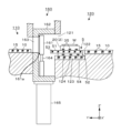
図4、図5の縦断側面図に示すように、真空搬送室120の床面部10には、当該真空搬送室120から見て手前側の領域に、橋渡しモジュール5を収容するための凹部状の収容領域122が形成されている。収容領域122の底面部123には、複数の走行面側コイル124が配列され、不図示の電力供給部から電力が供給されることにより磁場を発生する。走行面側コイル124は、底面部123に橋渡しモジュール5の走行面を形成するための橋渡しモジュール5用の走行面側磁石に相当する。
基台板52の内部には、例えば永久磁石により構成される複数のモジュール側磁石54が配列されている。モジュール側磁石54に対しては、走行面側コイル124によって生成される磁場との間に反発力が働く。この作用により底面部123の走行面側コイル124が設けられた領域に設定された走行面にて橋渡しモジュール5を磁気浮上させ、所望の方向に移動させることや、浮上量の調節などを行うことができる。
初めに、ロードポート141に対し、処理対象のウエハWを収容したキャリアCが載置されると、大気搬送室140内のウエハ搬送機構142によって、キャリアCからウエハWが取り出される。次いで、ウエハWは、アライメント室150に搬送されてアライメントが行われる。さらにウエハ搬送機構142によりアライメント室150からウエハWが取り出されると、ウエハ処理システム100の手前側から見て左右いずれかのロードロック室130のゲートバルブ133が開かれる。
しかる後、ウエハWを保持した第1の搬送モジュール20は、進入時とは反対の順序で橋渡しモジュール5を用いてロードロック室130から退出する。
以上に説明した橋渡しモジュール5の動作は、非走行領域を介した真空搬送室120と処理位置との間のウエハWの搬送を補助する搬送補助機構の役割を果たしている。
一方、載置台111上に載置されたウエハWは、ヒータにより加熱され、処理ガス供給部を介して処理ガスを供給し、また必要に応じて処理ガスをプラズマ化することにより、所定の処理が実行される。
さらに、ロードロック室130の雰囲気を大気圧雰囲気に切り替えた後、大気搬送室140側のウエハ搬送機構142によりロードロック室130内のウエハWを取り出し、所定のキャリアCに戻す。
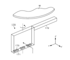
図1及び図6、図7に示すように、第2の搬送モジュール30は、第1の搬送モジュール20とほぼ同じ幅寸法を有する角板状の浮上体部31を備える。この浮上体部31に対しては、横方向に延在するように設けられ、ウエハWを水平に保持するアーム部32が設けられている。アーム部32の先端部には、3本の昇降ピン41、131が設けられた領域を左右から囲むように配置可能なフォークが設けられている。フォークは、第2の搬送モジュール30における基板保持部に相当する。
処理室内基板搬送部の構成例としては、図8A~図9Bを用いて説明するウエハ支持モジュール170を用いる場合と、図10A~図10Cを用いて説明する処理室内伸縮アーム180を用いる場合との2例について説明する。
図8A~図9Bには、処理室内基板搬送部の一の構成例であるウエハ支持モジュール170を設けた例を示している。これらの図には、図示を省略してあるが、ウエハ処理室110の床面部10には、例えば図4に示すウエハ処理室110の床面部と同様に、複数の走行面側コイル15が配列されている。
上述した構成のウエハ支持モジュール170によれば、磁気浮上によって移動する2つのウエハ支持モジュール170が互いに協働し、各々の支持部172に共通のウエハWを支持することができる。これら2つのウエハ支持モジュール170が、本実施の形態の処理室内基板搬送部に相当する。
図8Aにおいて、ウエハWの処理の期間中、ウエハ支持モジュール170は、ウエハ処理室110内で待機している。このとき、処理ガスやプラズマなどの影響を避けるために、シャッターを用いて、ウエハ支持モジュール170の待機領域とウエハWの処理空間とを区画してもよい。
また、ウエハ処理室110へのウエハWの搬入時には、上述の動作とは反対の手順で搬送が行われる。
処理室内伸縮アーム180は、ウエハWを保持した状態で伸縮自在な多関節アームとして構成されている。処理室内伸縮アーム180は、ウエハ処理室110内に配置され、ウエハWの処理位置となる載置台111と、ゲートバルブ160との間の領域に配置される。ここで、ウエハWの処理の期間中にウエハ処理室110に供給される処理ガスやプラズマなどの影響を避けるためにシャッター113を設けてもよい(図10B、図10C)。シャッター113は、処理位置に配置されたウエハWの処理の期間中に、ウエハWの処理が行われている空間と、シャッター113が配置されている空間とを区画する役割を果たす。
搬送対象のウエハWの処理が終わったら、昇降ピン112によりウエハWを突き上げて上昇させる。しかる後、載置台111側へ向けて処理室内伸縮アーム180を伸張させ、処理室内伸縮アーム180の先端に設けられたウエハ保持部をウエハWの下方側へ進入させる。その後、ウエハWを降下させることにより、昇降ピン112から処理室内伸縮アーム180にウエハWが受け渡される(図10A)。
また、ウエハ処理室110へのウエハWの搬入時には、上述の動作とは反対の手順で搬送が行われる。
なお、図1においては、後段側のウエハ処理室110及び中央のロードロック室130内におけるウエハ支持モジュール170や処理室内伸縮アーム180の記載は省略してある。
既述の第1の搬送モジュール20を用いたウエハWの搬送の場合と同様の手順により、手前側から見て中央のロードロック室130に処理対象のウエハWが搬入される。このロードロック室130の内部が真空雰囲気となったら、真空搬送室120側のゲートバルブ132が開かれる。そして、ロードロック室130内に設けられたウエハ支持モジュール170または処理室内伸縮アーム180を用い、真空搬送室120側に配置されたウエハ受け渡し部4にウエハWを受け渡す。
このとき、図10Cに示すように、ウエハ処理室110を斜め前方に見ながら昇降ピン41の配置領域へ向けて進入、または退出するように、第2の搬送モジュール30の移動経路を設定してもよい。この経路設定により、ウエハ処理室110に正対する方向から進入、または退出するように経路を設定する場合と比較して、第2の搬送モジュール30の移動経路がコンパクトになり、真空搬送室120の大型化を抑制することができる。
また、角板状の第1の搬送モジュール20を用い、搬送補助機構であるウエハ受け渡し部4と処理室内基板搬送部(ウエハ支持モジュール170、処理室内伸縮アーム180)とを利用してウエハWの搬送を行うことも可能である。
なお、図11に示すウエハ処理システム100aにおいても、第1の搬送モジュール20を用いてウエハWの搬送を行ってもよいし、橋渡しモジュール5を用いて搬送モジュール20、30を進入させるウエハ処理室110を併設してもよい。
図13は、真空搬送室120を構成する筐体の外面側にて床面部10aを構成した例を示している。図14に示すように、真空搬送室120の下面は、補強リブ102によって格子状に区画されており、各区画内にタイル101が配置されている。これらのタイル101には、図3、図7などに示す走行面側コイル15が配置されている。これらの走行面側コイル15は、不図示の電力供給部から電力が供給されることにより、第1の搬送モジュール20や第2の搬送モジュール30を磁気浮上させるための磁場を発生させることは既述の通りである。
なお、真空搬送室120の強度向上の観点のみからは、補強リブ102とタイル101とを組み合わせて構成される床面部10aは、真空搬送室120内に配置してもよい。
10 床面部
15 走行面側コイル
100、100a
ウエハ処理システム
110 ウエハ処理室
120、120a 真空搬送室
121 開口部
160 ゲートバルブ
20 第1の搬送モジュール
30 第2の搬送モジュール
35 モジュール側磁石
5 橋渡しモジュール
9 制御部
Claims (6)
- 基板処理室に対して基板を搬送して基板の処理を行う装置であって、
走行面側磁石が設けられた床面部と、前記基板処理室との間で基板の搬入出が行われる開口部が形成された側壁部とを有する基板搬送室と、
前記基板を保持する基板保持部と、前記走行面側磁石との間に反発力が働く浮上体側磁石と、を備え、前記反発力を用いた磁気浮上により、前記走行面側磁石が設けられた領域に形成された走行面を移動可能に構成された基板搬送モジュールと、
前記開口部を開閉すると共に、前記基板搬送モジュールが、前記磁気浮上により移動することのできない非走行領域を成すゲートバルブを介して前記基板搬送室に接続された前記基板処理室と、
基板搬送モジュールにより搬送される基板についての、前記非走行領域を介した前記基板搬送室と前記基板処理室内の基板の処理位置との間の搬送を補助する搬送補助機構と、を備え、
前記搬送補助機構は、前記走行面側磁石が設けられ、前記基板搬送室の前記床面部に収容された状態にて前記床面部と一体の前記走行面を形成する収容位置と、前記ゲートバルブが開状態にあるとき、前記非走行領域を覆うように前記走行面を形成する橋渡し位置との間を、前記基板搬送モジュールを載せた状態で移動自在に構成された橋渡しモジュールである、装置。 - 前記基板処理室の床面部には、前記走行面側磁石が設けられ、前記基板搬送モジュールは、前記橋渡し位置に移動した前記橋渡しモジュールと、前記基板処理室の内部との間を移動することにより、前記基板搬送室と前記基板処理室との間の基板の搬送を行う、請求項1に記載の装置。
- 前記基板搬送室の床面部には、前記橋渡しモジュールが収容される凹部状の収容領域が形成され、前記収容領域の底面部には、前記橋渡しモジュールを前記収容位置と前記橋渡し位置との間で移動させる走行面を形成するための橋渡しモジュール用の走行面側磁石が設けられていることと、
前記橋渡しモジュールには、前記橋渡しモジュール用の走行面側磁石との間に働く反発力を用いた磁気浮上を行うための、橋渡しモジュール用の浮上体側磁石が設けられていることと、を備えた、請求項1または2に記載の装置。 - 基板の処理が行われる基板処理室に対して基板を搬送する方法であって、
走行面側磁石が設けられた床面部と、前記基板処理室との間で基板の搬入出が行われる開口部が形成された側壁部とを有する基板搬送室内にて、前記基板を保持する基板保持部と、前記走行面側磁石との間に反発力が働く浮上体側磁石と、を備え、前記反発力を用いた磁気浮上により、前記走行面側磁石が設けられた領域に形成された走行面を移動可能に構成された基板搬送モジュールを用いて基板を搬送する工程と、
前記開口部を開閉すると共に、前記基板搬送モジュールが、前記磁気浮上により移動することのできない非走行領域を成すゲートバルブを介して前記基板処理室に接続された前記基板処理室に対し、基板搬送モジュールにより搬送される基板について、搬送補助機構を用いて、前記非走行領域を介した前記基板搬送室と前記基板処理室内の基板の処理位置との間の搬送を補助する工程と、を含み、
前記搬送補助機構は、前記走行面側磁石が設けられた橋渡しモジュールであり、前記補助する工程では、前記基板搬送室の前記床面部に収容された状態にて前記床面部と一体の前記走行面を形成する収容位置と、前記ゲートバルブが開状態にあるとき、前記非走行領域を覆うように前記走行面を形成する橋渡し位置との間を、前記基板搬送モジュールを載せた状態で移動する、方法。 - 前記基板処理室の床面部には前記走行面側磁石が設けられ、前記橋渡し位置に移動した前記橋渡しモジュールと、前記基板処理室の内部との間を前記基板搬送モジュールが移動することにより、前記基板搬送室と前記基板処理室との間の基板の搬送を行う工程を含む、請求項4に記載の方法。
- 前記基板搬送室の床面部には、前記橋渡しモジュールが収容される凹部状の収容領域が形成され、前記収容領域の底面部には、前記橋渡しモジュールを移動させる走行面を形成するための橋渡しモジュール用の走行面側磁石が設けられ、前記橋渡しモジュールには、前記橋渡しモジュール用の走行面側磁石との間に働く反発力を用いた磁気浮上を行うための、橋渡しモジュール用の浮上体側磁石が設けられ、
前記補助する工程では、前記橋渡しモジュールは、前記収容領域の前記走行面に沿って前記収容位置と前記橋渡し位置との間を移動する、請求項4または5に記載の方法。
Priority Applications (6)
| Application Number | Priority Date | Filing Date | Title |
|---|---|---|---|
| JP2021042787A JP7608898B2 (ja) | 2021-03-16 | 2021-03-16 | 基板を処理する装置及び基板を搬送する方法 |
| KR1020220027984A KR102669082B1 (ko) | 2021-03-16 | 2022-03-04 | 기판을 처리하는 장치 및 기판을 반송하는 방법 |
| US17/653,889 US11961758B2 (en) | 2021-03-16 | 2022-03-08 | Apparatus for processing substrate and method of transferring substrate |
| US18/609,164 US20240222186A1 (en) | 2021-03-16 | 2024-03-19 | Apparatus for processing substrate and method of transferring substrate |
| KR1020240064384A KR20240076405A (ko) | 2021-03-16 | 2024-05-17 | 기판을 처리하는 장치 및 기판을 반송하는 방법 |
| JP2024222012A JP2025039578A (ja) | 2021-03-16 | 2024-12-18 | 基板を処理する装置及び基板を搬送する方法 |
Applications Claiming Priority (1)
| Application Number | Priority Date | Filing Date | Title |
|---|---|---|---|
| JP2021042787A JP7608898B2 (ja) | 2021-03-16 | 2021-03-16 | 基板を処理する装置及び基板を搬送する方法 |
Related Child Applications (1)
| Application Number | Title | Priority Date | Filing Date |
|---|---|---|---|
| JP2024222012A Division JP2025039578A (ja) | 2021-03-16 | 2024-12-18 | 基板を処理する装置及び基板を搬送する方法 |
Publications (2)
| Publication Number | Publication Date |
|---|---|
| JP2022142568A JP2022142568A (ja) | 2022-09-30 |
| JP7608898B2 true JP7608898B2 (ja) | 2025-01-07 |
Family
ID=83284085
Family Applications (2)
| Application Number | Title | Priority Date | Filing Date |
|---|---|---|---|
| JP2021042787A Active JP7608898B2 (ja) | 2021-03-16 | 2021-03-16 | 基板を処理する装置及び基板を搬送する方法 |
| JP2024222012A Pending JP2025039578A (ja) | 2021-03-16 | 2024-12-18 | 基板を処理する装置及び基板を搬送する方法 |
Family Applications After (1)
| Application Number | Title | Priority Date | Filing Date |
|---|---|---|---|
| JP2024222012A Pending JP2025039578A (ja) | 2021-03-16 | 2024-12-18 | 基板を処理する装置及び基板を搬送する方法 |
Country Status (3)
| Country | Link |
|---|---|
| US (2) | US11961758B2 (ja) |
| JP (2) | JP7608898B2 (ja) |
| KR (2) | KR102669082B1 (ja) |
Families Citing this family (11)
| Publication number | Priority date | Publication date | Assignee | Title |
|---|---|---|---|---|
| IT201900010536A1 (it) * | 2019-07-01 | 2021-01-01 | Ima Spa | Macchina e procedimento per trasportare automaticamente uno o piu’ componenti per realizzare una confezione da e verso una o piu’ stazioni di lavorazione. |
| JP7537847B2 (ja) * | 2021-03-02 | 2024-08-21 | 東京エレクトロン株式会社 | 基板搬送装置及び基板処理システム |
| JP7683294B2 (ja) * | 2021-04-19 | 2025-05-27 | 東京エレクトロン株式会社 | 基板を搬送する装置、及び基板を搬送する方法 |
| JP7771651B2 (ja) * | 2021-11-12 | 2025-11-18 | 東京エレクトロン株式会社 | 基板搬送装置及び基板搬送方法 |
| JP2023130880A (ja) * | 2022-03-08 | 2023-09-21 | 東京エレクトロン株式会社 | 基板処理室内に配置される部材を搬送する装置、基板処理システム及び前記部材を搬送する方法 |
| JP2023139392A (ja) * | 2022-03-22 | 2023-10-04 | 東京エレクトロン株式会社 | 基板処理システム |
| JP2024051304A (ja) * | 2022-09-30 | 2024-04-11 | 東京エレクトロン株式会社 | 基板搬送モジュール及び基板搬送方法 |
| US20240153802A1 (en) * | 2022-11-07 | 2024-05-09 | Applied Materials, Inc. | Semiconductor process equipment |
| IT202200026922A1 (it) * | 2022-12-28 | 2024-06-28 | Ima Spa | Apparecchiatura e procedimento per movimentare automaticamente oggetti nell’ambito di un ambiente con atmosfera controllata. |
| WO2025217354A1 (en) * | 2024-04-10 | 2025-10-16 | Brooks Automation Us, Llc | Substrate handler end effector vibration isolation and method therfor |
| JP2025187956A (ja) * | 2024-06-14 | 2025-12-25 | ヴイエム インコーポレイテッド | 基板移送装置 |
Citations (4)
| Publication number | Priority date | Publication date | Assignee | Title |
|---|---|---|---|---|
| JP2011222825A (ja) | 2010-04-12 | 2011-11-04 | Tokyo Electron Ltd | 被処理体処理装置 |
| JP2013239746A (ja) | 2008-12-19 | 2013-11-28 | Nikon Corp | 露光装置 |
| US20160218029A1 (en) | 2015-01-23 | 2016-07-28 | Applied Materials, Inc. | Semiconductor process equipment |
| JP2021086986A (ja) | 2019-11-29 | 2021-06-03 | 東京エレクトロン株式会社 | 基板搬送装置及び基板処理システム |
Family Cites Families (7)
| Publication number | Priority date | Publication date | Assignee | Title |
|---|---|---|---|---|
| JPH0514412A (ja) * | 1991-07-05 | 1993-01-22 | Toshiba Corp | 発着信装置 |
| JP2751975B2 (ja) * | 1991-12-20 | 1998-05-18 | 株式会社日立製作所 | 半導体処理装置のロードロック室 |
| JPH0614412A (ja) * | 1992-06-25 | 1994-01-21 | Ntn Corp | 磁気浮上搬送装置 |
| JPH07115120A (ja) * | 1993-10-18 | 1995-05-02 | Hitachi Ltd | 基板搬送装置およびその方法 |
| CN1996552B (zh) * | 2001-08-31 | 2012-09-05 | 克罗辛自动化公司 | 晶片机 |
| US7988398B2 (en) * | 2002-07-22 | 2011-08-02 | Brooks Automation, Inc. | Linear substrate transport apparatus |
| KR102166910B1 (ko) | 2017-10-27 | 2020-10-16 | 어플라이드 머티어리얼스, 인코포레이티드 | 증착 시스템 내에서의 비접촉식 이송을 위한 캐리어, 캐리어의 비접촉식 이송을 위한 장치, 및 증착 시스템 내에서의 캐리어의 비접촉식 이송을 위한 방법 |
-
2021
- 2021-03-16 JP JP2021042787A patent/JP7608898B2/ja active Active
-
2022
- 2022-03-04 KR KR1020220027984A patent/KR102669082B1/ko active Active
- 2022-03-08 US US17/653,889 patent/US11961758B2/en active Active
-
2024
- 2024-03-19 US US18/609,164 patent/US20240222186A1/en active Pending
- 2024-05-17 KR KR1020240064384A patent/KR20240076405A/ko active Pending
- 2024-12-18 JP JP2024222012A patent/JP2025039578A/ja active Pending
Patent Citations (5)
| Publication number | Priority date | Publication date | Assignee | Title |
|---|---|---|---|---|
| JP2013239746A (ja) | 2008-12-19 | 2013-11-28 | Nikon Corp | 露光装置 |
| JP2011222825A (ja) | 2010-04-12 | 2011-11-04 | Tokyo Electron Ltd | 被処理体処理装置 |
| US20160218029A1 (en) | 2015-01-23 | 2016-07-28 | Applied Materials, Inc. | Semiconductor process equipment |
| JP2018504784A (ja) | 2015-01-23 | 2018-02-15 | アプライド マテリアルズ インコーポレイテッドApplied Materials,Incorporated | 半導体処理設備 |
| JP2021086986A (ja) | 2019-11-29 | 2021-06-03 | 東京エレクトロン株式会社 | 基板搬送装置及び基板処理システム |
Also Published As
| Publication number | Publication date |
|---|---|
| JP2022142568A (ja) | 2022-09-30 |
| KR20240076405A (ko) | 2024-05-30 |
| KR102669082B1 (ko) | 2024-05-27 |
| US20220301921A1 (en) | 2022-09-22 |
| US20240222186A1 (en) | 2024-07-04 |
| US11961758B2 (en) | 2024-04-16 |
| KR20220129466A (ko) | 2022-09-23 |
| JP2025039578A (ja) | 2025-03-21 |
Similar Documents
| Publication | Publication Date | Title |
|---|---|---|
| JP7608898B2 (ja) | 基板を処理する装置及び基板を搬送する方法 | |
| JP6582676B2 (ja) | ロードロック装置、及び基板処理システム | |
| JP7596670B2 (ja) | 基板を処理する装置、及び基板を処理する方法 | |
| JP7679629B2 (ja) | 基板の搬送を行う装置、基板を処理するシステム及び基板を処理する方法 | |
| US20250372427A1 (en) | Substrate Processing System | |
| US20240290645A1 (en) | Apparatus for transporting substrate, system for processing substrate, and method of transporting substrate | |
| KR20260002337A (ko) | 기판 반송 모듈 및 기판 반송 방법 | |
| KR20230132374A (ko) | 기판 처리실 내에 배치되는 부재를 반송하는 장치, 기판 처리 시스템 및 상기 부재를 반송하는 방법 | |
| TWI631581B (zh) | 磁化處理裝置及磁化處理方法 |
Legal Events
| Date | Code | Title | Description |
|---|---|---|---|
| A621 | Written request for application examination |
Free format text: JAPANESE INTERMEDIATE CODE: A621 Effective date: 20231218 |
|
| A977 | Report on retrieval |
Free format text: JAPANESE INTERMEDIATE CODE: A971007 Effective date: 20240909 |
|
| A131 | Notification of reasons for refusal |
Free format text: JAPANESE INTERMEDIATE CODE: A131 Effective date: 20240917 |
|
| A521 | Request for written amendment filed |
Free format text: JAPANESE INTERMEDIATE CODE: A523 Effective date: 20241030 |
|
| TRDD | Decision of grant or rejection written | ||
| A01 | Written decision to grant a patent or to grant a registration (utility model) |
Free format text: JAPANESE INTERMEDIATE CODE: A01 Effective date: 20241119 |
|
| A61 | First payment of annual fees (during grant procedure) |
Free format text: JAPANESE INTERMEDIATE CODE: A61 Effective date: 20241202 |
|
| R150 | Certificate of patent or registration of utility model |
Ref document number: 7608898 Country of ref document: JP Free format text: JAPANESE INTERMEDIATE CODE: R150 |