WO2022113161A1 - 感光性樹脂組成物、感光性エレメント、レジストパターンの形成方法及びプリント配線板の製造方法 - Google Patents
感光性樹脂組成物、感光性エレメント、レジストパターンの形成方法及びプリント配線板の製造方法 Download PDFInfo
- Publication number
- WO2022113161A1 WO2022113161A1 PCT/JP2020/043605 JP2020043605W WO2022113161A1 WO 2022113161 A1 WO2022113161 A1 WO 2022113161A1 JP 2020043605 W JP2020043605 W JP 2020043605W WO 2022113161 A1 WO2022113161 A1 WO 2022113161A1
- Authority
- WO
- WIPO (PCT)
- Prior art keywords
- resin composition
- meth
- photosensitive
- photosensitive resin
- mass
- Prior art date
- Legal status (The legal status is an assumption and is not a legal conclusion. Google has not performed a legal analysis and makes no representation as to the accuracy of the status listed.)
- Ceased
Links
Images
Classifications
-
- G—PHYSICS
- G03—PHOTOGRAPHY; CINEMATOGRAPHY; ANALOGOUS TECHNIQUES USING WAVES OTHER THAN OPTICAL WAVES; ELECTROGRAPHY; HOLOGRAPHY
- G03F—PHOTOMECHANICAL PRODUCTION OF TEXTURED OR PATTERNED SURFACES, e.g. FOR PRINTING, FOR PROCESSING OF SEMICONDUCTOR DEVICES; MATERIALS THEREFOR; ORIGINALS THEREFOR; APPARATUS SPECIALLY ADAPTED THEREFOR
- G03F7/00—Photomechanical, e.g. photolithographic, production of textured or patterned surfaces, e.g. printing surfaces; Materials therefor, e.g. comprising photoresists; Apparatus specially adapted therefor
- G03F7/004—Photosensitive materials
- G03F7/027—Non-macromolecular photopolymerisable compounds having carbon-to-carbon double bonds, e.g. ethylenic compounds
- G03F7/032—Non-macromolecular photopolymerisable compounds having carbon-to-carbon double bonds, e.g. ethylenic compounds with binders
- G03F7/033—Non-macromolecular photopolymerisable compounds having carbon-to-carbon double bonds, e.g. ethylenic compounds with binders the binders being polymers obtained by reactions only involving carbon-to-carbon unsaturated bonds, e.g. vinyl polymers
-
- G—PHYSICS
- G03—PHOTOGRAPHY; CINEMATOGRAPHY; ANALOGOUS TECHNIQUES USING WAVES OTHER THAN OPTICAL WAVES; ELECTROGRAPHY; HOLOGRAPHY
- G03F—PHOTOMECHANICAL PRODUCTION OF TEXTURED OR PATTERNED SURFACES, e.g. FOR PRINTING, FOR PROCESSING OF SEMICONDUCTOR DEVICES; MATERIALS THEREFOR; ORIGINALS THEREFOR; APPARATUS SPECIALLY ADAPTED THEREFOR
- G03F7/00—Photomechanical, e.g. photolithographic, production of textured or patterned surfaces, e.g. printing surfaces; Materials therefor, e.g. comprising photoresists; Apparatus specially adapted therefor
- G03F7/004—Photosensitive materials
-
- G—PHYSICS
- G03—PHOTOGRAPHY; CINEMATOGRAPHY; ANALOGOUS TECHNIQUES USING WAVES OTHER THAN OPTICAL WAVES; ELECTROGRAPHY; HOLOGRAPHY
- G03F—PHOTOMECHANICAL PRODUCTION OF TEXTURED OR PATTERNED SURFACES, e.g. FOR PRINTING, FOR PROCESSING OF SEMICONDUCTOR DEVICES; MATERIALS THEREFOR; ORIGINALS THEREFOR; APPARATUS SPECIALLY ADAPTED THEREFOR
- G03F7/00—Photomechanical, e.g. photolithographic, production of textured or patterned surfaces, e.g. printing surfaces; Materials therefor, e.g. comprising photoresists; Apparatus specially adapted therefor
- G03F7/004—Photosensitive materials
- G03F7/0045—Photosensitive materials with organic non-macromolecular light-sensitive compounds not otherwise provided for, e.g. dissolution inhibitors
-
- G—PHYSICS
- G03—PHOTOGRAPHY; CINEMATOGRAPHY; ANALOGOUS TECHNIQUES USING WAVES OTHER THAN OPTICAL WAVES; ELECTROGRAPHY; HOLOGRAPHY
- G03F—PHOTOMECHANICAL PRODUCTION OF TEXTURED OR PATTERNED SURFACES, e.g. FOR PRINTING, FOR PROCESSING OF SEMICONDUCTOR DEVICES; MATERIALS THEREFOR; ORIGINALS THEREFOR; APPARATUS SPECIALLY ADAPTED THEREFOR
- G03F7/00—Photomechanical, e.g. photolithographic, production of textured or patterned surfaces, e.g. printing surfaces; Materials therefor, e.g. comprising photoresists; Apparatus specially adapted therefor
- G03F7/004—Photosensitive materials
- G03F7/027—Non-macromolecular photopolymerisable compounds having carbon-to-carbon double bonds, e.g. ethylenic compounds
-
- G—PHYSICS
- G03—PHOTOGRAPHY; CINEMATOGRAPHY; ANALOGOUS TECHNIQUES USING WAVES OTHER THAN OPTICAL WAVES; ELECTROGRAPHY; HOLOGRAPHY
- G03F—PHOTOMECHANICAL PRODUCTION OF TEXTURED OR PATTERNED SURFACES, e.g. FOR PRINTING, FOR PROCESSING OF SEMICONDUCTOR DEVICES; MATERIALS THEREFOR; ORIGINALS THEREFOR; APPARATUS SPECIALLY ADAPTED THEREFOR
- G03F7/00—Photomechanical, e.g. photolithographic, production of textured or patterned surfaces, e.g. printing surfaces; Materials therefor, e.g. comprising photoresists; Apparatus specially adapted therefor
- G03F7/004—Photosensitive materials
- G03F7/027—Non-macromolecular photopolymerisable compounds having carbon-to-carbon double bonds, e.g. ethylenic compounds
- G03F7/028—Non-macromolecular photopolymerisable compounds having carbon-to-carbon double bonds, e.g. ethylenic compounds with photosensitivity-increasing substances, e.g. photoinitiators
- G03F7/031—Organic compounds not covered by group G03F7/029
-
- H—ELECTRICITY
- H05—ELECTRIC TECHNIQUES NOT OTHERWISE PROVIDED FOR
- H05K—PRINTED CIRCUITS; CASINGS OR CONSTRUCTIONAL DETAILS OF ELECTRIC APPARATUS; MANUFACTURE OF ASSEMBLAGES OF ELECTRICAL COMPONENTS
- H05K3/00—Apparatus or processes for manufacturing printed circuits
- H05K3/02—Apparatus or processes for manufacturing printed circuits in which the conductive material is applied to the surface of the insulating support and is thereafter removed from such areas of the surface which are not intended for current conducting or shielding
- H05K3/06—Apparatus or processes for manufacturing printed circuits in which the conductive material is applied to the surface of the insulating support and is thereafter removed from such areas of the surface which are not intended for current conducting or shielding the conductive material being removed chemically or electrolytically, e.g. by photo-etch process
-
- H—ELECTRICITY
- H05—ELECTRIC TECHNIQUES NOT OTHERWISE PROVIDED FOR
- H05K—PRINTED CIRCUITS; CASINGS OR CONSTRUCTIONAL DETAILS OF ELECTRIC APPARATUS; MANUFACTURE OF ASSEMBLAGES OF ELECTRICAL COMPONENTS
- H05K3/00—Apparatus or processes for manufacturing printed circuits
- H05K3/10—Apparatus or processes for manufacturing printed circuits in which conductive material is applied to the insulating support in such a manner as to form the desired conductive pattern
- H05K3/18—Apparatus or processes for manufacturing printed circuits in which conductive material is applied to the insulating support in such a manner as to form the desired conductive pattern using precipitation techniques to apply the conductive material
Definitions
- the present disclosure relates to a photosensitive resin composition, a photosensitive element, a method for forming a resist pattern, and a method for manufacturing a printed wiring board.
- a photosensitive resin composition is used as a resist material used for an etching treatment or a plating treatment, and a layer formed on a support film using the photosensitive resin composition (hereinafter, “photosensitive”).
- Photosensitive elements with also referred to as "layers" are widely used.
- the printed wiring board is manufactured by the following procedure, for example, using the above-mentioned photosensitive element. That is, first, the photosensitive layer of the photosensitive element is laminated on a circuit-forming substrate such as a copper-clad laminate. Next, the photosensitive layer is exposed via a mask film or the like to form a photocurable portion. At this time, the support film is peeled off before or after the exposure. Then, the region other than the light-cured portion of the photosensitive layer is removed with a developing solution to form a resist pattern. Next, using the resist pattern as a resist, an etching treatment or a plating treatment is performed to form a conductor pattern, and finally the photocured portion (resist pattern) of the photosensitive layer is peeled off (removed).
- the photosensitive layer is required to have excellent characteristics in the etching treatment or the plating treatment, excellent adhesion to the circuit forming substrate, and excellent resolution in forming the resist pattern.
- Patent Document 1 discloses a photosensitive resin composition having excellent sensitivity and resolution by using a specific sensitizing dye.
- Patent Document 2 discloses a photosensitive resin composition having excellent sensitivity and resolution by using a specific alkali-soluble polymer and a compound having an ethylenic double bond.
- the photosensitive layer When laminating the photosensitive layer of the photosensitive element on the circuit forming substrate, if the photosensitive layer has low followability to the circuit forming substrate, a fine void is generated between the photosensitive layer and the circuit forming substrate. , May affect the formation of conductor patterns. Therefore, the photosensitive layer is required to have excellent followability to the circuit forming substrate.
- the present disclosure discloses a photosensitive resin composition capable of forming a photosensitive layer having excellent followability to a circuit forming substrate, a photosensitive element using the photosensitive resin composition, a method for forming a resist pattern, and a printed wiring board. It is an object of the present invention to provide the manufacturing method of.
- the photosensitive resin composition according to the present disclosure contains a binder polymer, a photopolymerizable compound, and a photopolymerization initiator, and the binder polymer is a structural unit derived from a polymerizable monomer having a carboxy group (a structural unit ().
- A1 a structural unit (a2) derived from styrene or a styrene derivative, a structural unit (a3) derived from an alkyl (meth) acrylic rate having an alkyl group having 1 to 3 carbon atoms, and 4 to 4 carbon atoms. It has a structural unit (a4) derived from an alkyl (meth) methacrylate having 12 alkyl groups.
- the photosensitive element according to the present disclosure includes a support and a photosensitive layer formed on the support, and the photosensitive layer contains the above-mentioned photosensitive resin composition.
- the method for forming a resist pattern according to the present disclosure includes a step of forming a photosensitive layer on a substrate by using the above-mentioned photosensitive resin composition or a photosensitive element, and irradiation of at least a part of the photosensitive layer with active light.
- the process includes a step of forming a photo-cured portion and a step of removing at least a part of the unphoto-cured portion of the photosensitive layer from the substrate.
- the method for manufacturing a printed wiring board according to the present disclosure includes a step of forming a conductor pattern by etching or plating a substrate on which a resist pattern is formed by the method for forming a resist pattern.
- a photosensitive resin composition capable of forming a photosensitive layer having excellent followability to a circuit forming substrate, a photosensitive element using the photosensitive resin composition, a method for forming a resist pattern, and printing.
- a method for manufacturing a wiring board can be provided.
- the term "process” is included in this term not only as an independent process but also as long as the intended action of the process is achieved even if it cannot be clearly distinguished from other processes. Is done.
- the term "layer” includes not only a structure having a shape formed on the entire surface but also a structure having a shape partially formed when observed as a plan view.
- the numerical range indicated by using "-" indicates a range including the numerical values before and after "-" as the minimum value and the maximum value, respectively.
- the upper limit value or the lower limit value of the numerical range of one step may be replaced with the upper limit value or the lower limit value of the numerical range of another step.
- the upper limit value or the lower limit value of the numerical range may be replaced with the value shown in the examples.
- (meth) acrylic acid means at least one of “acrylic acid” and the corresponding “methacrylic acid”, and the same applies to other similar expressions such as (meth) acrylate.
- the “solid content” is a non-volatile substance excluding volatile substances such as water and solvent contained in the photosensitive resin composition, and is volatile when the resin composition is dried. It shows the components that remain without leaving, and also includes liquid, water candy-like, and wax-like substances at room temperature around 25 ° C.
- the photosensitive resin composition according to the present embodiment contains a binder polymer, a photopolymerizable compound, and a photopolymerization initiator, and the binder polymer is a structural unit derived from a polymerizable monomer having a carboxy group.
- A1 a structural unit (a2) derived from styrene or a styrene derivative, a structural unit (a3) derived from an alkyl (meth) acrylic rate having an alkyl group having 1 to 3 carbon atoms, and 4 carbon atoms. It has a structural unit (a4) derived from an alkyl (meth) methacrylate having up to 12 alkyl groups.
- the component (A) component includes a structural unit (a1) having a carboxy group, a structural unit (a2) derived from styrene or a styrene derivative, and an alkyl (meth) having an alkyl group having 1 to 3 carbon atoms.
- the binder polymer has a structural unit (a1) from the viewpoint of alkali developability.
- the polymerizable monomer having a carboxy group include (meth) acrylic acid, ⁇ -bromoacrylic acid, ⁇ -chloroacrylic acid, ⁇ -furyl (meth) acrylic acid, ⁇ -styryl (meth) acrylic acid, and the like.
- Maleic acid monoesters such as maleic acid, maleic acid anhydride, monomethyl maleate, monoethyl maleate, monoisopropyl maleate, fumaric acid, silicic acid, ⁇ -cyanosilicic acid, itaconic acid, crotonic acid, and propioleic acid Can be mentioned.
- the polymerizable monomer having a carboxy group may be (meth) acrylic acid or methacrylic acid from the viewpoint of further improving the alkali developability.
- the content of the structural unit (a1) is 10 to 30% by mass, 15 to 28% by mass, or 20 based on the total amount of the component (A) from the viewpoint of improving the alkali developability and the followability in a well-balanced manner. It may be up to 26% by mass.
- the content of the structural unit (a1) is 10% by mass or more, the alkali developability tends to be improved, and when the content is 30% by mass or less, the followability tends to be excellent.
- the binder polymer has a structural unit (a2) from the viewpoint of resolution.
- the styrene derivative is a polymerizable compound in which a hydrogen atom in the ⁇ -position or aromatic ring of styrene such as vinyltoluene and ⁇ -methylstyrene is substituted.
- the content of the structural unit (a2) in the component (A) is 10 to 50% by mass and 12 to 45 based on the total amount of the component (A). It may be% by mass, or 14 to 44% by mass.
- the binder polymer has a structural unit (a3) from the viewpoint of resolution.
- alkyl (meth) acrylic rate having an alkyl group having 1 to 3 carbon atoms include methyl (meth) acrylate, ethyl (meth) acrylate, and propyl (meth) acrylate.
- the content of the structural unit (a3) in the component (A) is 5 to 70% by mass and 12 to 65 based on the total amount of the component (A) from the viewpoint of improving the alkali developability and the followability in a well-balanced manner. It may be% by mass, or 15 to 64% by mass.
- the content of the structural unit (a3) is 5% by mass or more, the alkali developability tends to be improved, and when the content is 70% by mass or less, the followability tends to be excellent.
- the binder polymer has a structural unit (a4) from the viewpoint of followability.
- the alkyl group having 4 to 12 carbon atoms may be a linear or branched alkyl group.
- Examples of the alkyl (meth) methacrylate having an alkyl group having 4 to 12 carbon atoms include butyl (meth) acrylate, pentyl (meth) acrylate, hexyl (meth) acrylate, heptyl (meth) acrylate, and octyl (meth) acrylate.
- 2-Ethylhexyl (meth) acrylate nonyl (meth) acrylate, decyl (meth) acrylate, undecyl (meth) acrylate, and dodecyl (meth) acrylate.
- the content of the structural unit (a4) in the component (A) is 0.5 to 30% by mass, 0, based on the total amount of the component (A). It may be 8 to 25% by mass, or 1 to 22% by mass.
- the component (A) may further have a structural unit (a5) other than the structural units (a1) to (a4).
- a structural unit (a5) examples include benzyl (meth) acrylate or a derivative thereof, acrylamide such as diacetoneacrylamide, and an ether compound of vinyl alcohol such as vinyl-n-butyl ether.
- the acid value of the component (A) is 100 mgKOH / g or more, 110 mgKOH / g or more, 120 mgKOH / g or more, or 130 mgKOH / g or more from the viewpoint of further improving the balance between developability, resolution and followability. May be good.
- the acid value of the component (A) may be 180 mgKOH / g or less, 170 mgKOH / g or less, 165 mgKOH / g or less, or 160 mgKOH / g or less from the viewpoint of further improving the followability of the photosensitive layer.
- the weight average molecular weight (Mw) of the component (A) may be 60,000 or less, 56,000 or less, 54,000 or less, or 52,000 or less in terms of further excellent developability.
- the Mw of the component (A) may be 10,000 or more, 15,000 or more, 20,000 or more, or 25,000 or more in terms of further excellent adhesion.
- the degree of dispersion (weight average molecular weight / number average molecular weight) of the component (A) may be 3.0 or less, 2.8 or less, or 2.5 or less in terms of further excellent resolution and adhesion. The resolution tends to improve as the degree of dispersion decreases.
- the weight average molecular weight and the number average molecular weight are measured by gel permeation chromatography (GPC) and are converted values using standard polystyrene as a standard sample.
- the glass transition temperature (Tg) of the component (A) may be 80 to 130 ° C., 85 to 125 ° C., or 90 to 120 ° C. from the viewpoint of further improving the followability.
- the component (A) one type can be used alone or two or more types can be used in combination.
- the component (A) includes, for example, two or more kinds of binder polymers composed of different polymerizable monomers, two or more kinds of binder polymers having different Mw, and different dispersities. Two or more kinds of binder polymers can be mentioned.
- the content of the component (A) is 30 to 80 parts by mass, 40 to 75 parts by mass, 50 to 70 parts by mass, or 50 to 60 parts by mass with respect to 100 parts by mass of the total amount of the component (A) and the component (B). It may be a department. When the content of the component (A) is within this range, the strength of the light-cured portion of the photosensitive layer becomes better.
- Component (B) photopolymerizable compound
- the component (B) is not particularly limited as long as it has at least one ethylenically unsaturated bond and is photopolymerizable.
- the ethylenically unsaturated bond is not particularly limited as long as photopolymerization is possible. Examples of the ethylenically unsaturated bond include ⁇ , ⁇ -unsaturated carbonyl groups such as (meth) acryloyl group.
- Examples of the photopolymerizable compound having an ⁇ , ⁇ -unsaturated carbonyl group include ⁇ , ⁇ -unsaturated carboxylic acid ester of a polyhydric alcohol, bisphenol type (meth) acrylate, and ⁇ , ⁇ -unmodified of a glycidyl group-containing compound.
- Examples include saturated carboxylic acid adducts, (meth) acrylates with urethane bonds, nonylphenoxypolyethyleneoxyacrylates, and (meth) acrylic acid alkyl esters.
- Examples of the ⁇ , ⁇ -unsaturated carboxylic acid ester of the polyhydric alcohol include polyethylene glycol di (meth) acrylate having an ethylene group number of 2 to 14, and polypropylene glycol di (meth) acrylate having a propylene group number of 2 to 14. Meta) acrylate, polyethylene / polypropylene glycol di (meth) acrylate, trimethylolpropane di (meth) acrylate, trimethylolpropane tri (meth) having 2 to 14 ethylene groups and 2 to 14 propylene groups.
- EO modification means having a block structure of ethylene oxide (EO) group
- PO modification means having a block structure of propylene oxide (PO) group.
- the component (B) may contain a polyalkylene glycol di (meth) acrylate from the viewpoint of improving the flexibility of the resist pattern.
- the polyalkylene glycol di (meth) acrylate may have at least one of an EO group and a PO group, and may have both an EO group and a PO group.
- the EO group and the PO group may be continuously present in a block or randomly.
- the PO group may be either an oxy-n-propylene group or an oxyisopropylene group.
- the secondary carbon of the propylene group may be bonded to the oxygen atom, or the primary carbon may be bonded to the oxygen atom.
- polyalkylene glycol di (meth) acrylate examples include, for example, FA-023M (manufactured by Showa Denko Materials Co., Ltd.), FA-024M (manufactured by Showa Denko Materials Co., Ltd.), and NK ester HEMA-9P (new). Nakamura Chemical Industry Co., Ltd.).
- the component (B) may contain (meth) acrylate having a urethane bond from the viewpoint of improving the flexibility of the resist pattern.
- the (meth) acrylate having a urethane bond include a (meth) acrylic monomer having an OH group at the ⁇ -position and a diisocyanate (isophorone diisocyanate, 2,6-toluene diisocyanate, 2,4-toluene diisocyanate, 1,6-hexa).
- Examples thereof include addition reactants with methylene diisocyanate), tris ((meth) acryloxytetraethylene glycol isocyanate) hexamethylene isocyanurate, EO-modified urethane di (meth) acrylate, and EO and PO-modified urethane di (meth) acrylate.
- Examples of commercially available products of EO-modified urethane di (meth) acrylate include “UA-11” and “UA-21EB” (manufactured by Shin-Nakamura Chemical Industry Co., Ltd.).
- Examples of commercially available products of EO and PO-modified urethane di (meth) acrylate include “UA-13” (manufactured by Shin-Nakamura Chemical Industry Co., Ltd.).
- the component (B) may contain dipentaerythritol or a (meth) acrylate compound having a skeleton derived from pentaerythritol from the viewpoint of easily forming a thick-film resist pattern and improving resolution and adhesion in a well-balanced manner.
- the (meth) acrylate compound having a skeleton derived from dipentaerythritol or pentaerythritol preferably has four or more (meth) acryloyl groups, and is preferably dipentaerythritol penta (meth) acrylate or dipentaerythritol hexa (meth) acrylate. May be.
- the component (B) may contain a bisphenol type (meth) acrylate, or may contain a bisphenol A type (meth) acrylate among the bisphenol type (meth) acrylates. ..
- the bisphenol A type (meth) acrylate include 2,2-bis (4-((meth) acryloxypolyethoxy) phenyl) propane and 2,2-bis (4-((meth) acryloxypolypropoxy)).
- 2,2-bis (4-((meth) acryloxipolyethoxy) phenyl) propane is preferable from the viewpoint of further improving the resolution and putter forming property.
- nonylphenoxypolyethyleneoxyacrylate examples include nonylphenoxytetraethyleneoxyacrylate, nonylphenoxypentaethyleneoxyacrylate, nonylphenoxyhexaethyleneoxyacrylate, nonylphenoxyheptaethyleneoxyacrylate, nonylphenoxyoctaethyleneoxyacrylate, and nonylphenoxynonaethyleneoxy.
- examples thereof include acrylate, nonylphenoxydecaethyleneoxyacrylate, and nonylphenoxyundecaethyleneoxyacrylate.
- the content of the component (B) is preferably 20 to 60 parts by mass, more preferably 30 to 55 parts by mass with respect to 100 parts by mass of the total amount of the component (A) and the component (B). It is more preferably 35 to 50 parts by mass.
- the content of the component (B) is in this range, the light sensitivity and the coating film property become better in addition to the resolution and adhesion of the photosensitive resin composition and the resist hem generation property.
- the component (C) is not particularly limited as long as it can polymerize the component (B), and can be appropriately selected from commonly used photopolymerization initiators. From the viewpoint of improving pattern formation, those that generate free radicals by active light, for example, acylphosphine oxide type, oxime ester type, aromatic ketone type, quinone type, alkylphenone type, imidazole type, aclysine type, phenylglycine. Examples thereof include photopolymerization initiators such as radicals and quinones.
- the component (C) may contain an acridine-based photopolymerization initiator, a phenylglycine-based photopolymerization initiator, or an imidazole-based photopolymerization initiator in terms of improving sensitivity and resolution in a well-balanced manner, and may contain an acridine-based photopolymerization initiator. Is preferably included.
- the component (C) one type can be used alone or two or more types can be used in combination.
- acridin-based photopolymerization initiator examples include 9-phenylacridines, 9- (p-methylphenyl) acridins, 9- (m-methylphenyl) acridins, 9- (p-chlorophenyl) acridins, and 9- (m-).
- Chlorophenyl) acridines 9-aminoacridines, 9-dimethylaminoacridines, 9-diethylaminoacridines, 9-pentylaminoacridines, 1,2-bis (9-acridinyl) ethane, 1,4-bis (9-acridinyl) butane, 1,6-bis (9-acridinyl) hexane, 1,8-bis (9-acridinyl) octane, 1,10-bis (9-acridinyl) decane, 1,12-bis (9-acridinyl) dodecane, 1, Bis (9) such as 14-bis (9-acridinyl) tetradecane, 1,16-bis (9-acridinyl) hexadecane, 1,18-bis (9-acridinyl) octadecane, 1,20-bis (9-acridinyl) icosane, etc.
- phenylglycine-based photopolymerization initiator examples include N-phenylglycine, N-methyl-N-phenylglycine, and N-ethyl-N-phenylglycine.
- imidazole-based photopolymerization initiator examples include 2- (o-chlorophenyl) -4,5-diphenylbiimidazole, 2,2', 5-tris- (o-chlorophenyl) -4- (3,4-dimethoxy).
- the content of the component (C) is 0.1 to 10 parts by mass, 0.2 to 5 parts by mass, and 0.4 to 3 parts by mass with respect to 100 parts by mass of the total amount of the component (A) and the component (B). , Or 0.5 to 2 parts by mass.
- the content of the component (C) is 0.1 parts by mass or more, the light sensitivity, resolution and adhesion tend to be improved, and when the content is 10 parts by mass or less, the resist pattern forming property tends to be better.
- the photosensitive resin composition according to the present embodiment may further contain a sensitizer having absorption at 340 to 430 nm as the component (D).
- a sensitizer having absorption at 340 to 430 nm as the component (D).
- the sensitizer include dialkylaminobenzophenone compounds, pyrazoline compounds, anthracene compounds, coumarin compounds, xanthone compounds, oxazole compounds, benzoxazole compounds, thiazole compounds, benzothiazole compounds, triazole compounds, stylben compounds, triazine compounds and thiophene compounds. , Naphthalimide compounds, and triarylamine compounds.
- the sensitizer may contain at least one selected from the group consisting of pyrazoline compounds, anthracene compounds, coumarin compounds, and triarylamine compounds from the viewpoint of sensitivity and adhesion, and may contain pyrazoline compounds, anthracene compounds, and coumarin compounds. It may contain at least one selected from the group consisting of.
- Examples of the pyrazoline compound include 1-phenyl-3- (4-methoxystyryl) -5- (4-methoxyphenyl) pyrazoline and 1-phenyl-3- (4-tert-butylstyryl) -5- (4-). Examples thereof include tert-butylphenyl) pyrazoline and 1-phenyl-3-biphenyl-5- (4-tert-butylphenyl) pyrazoline.
- Examples of the anthracene compound include 9,10-dibutoxyanthracene and 9,10-diphenylanthracene.
- Examples of the coumarin compound include 3-benzoyl-7-diethylaminocoumarin, 7-diethylamino-4-methylcoumarin, 3,3'-carbonylbis (7-diethylaminocoumarin), and 2,3,6,7-tetrahydro-. Examples thereof include 9-methyl-1H, 5H, 11H- [1] benzopyrano [6,7,8-ij] kilolysine-11-one.
- the content of the component (D) is 0.01 to 10% by mass and 0.05 to 5 based on the total solid content of the photosensitive resin composition. It may be% by mass, or 0.1 to 3% by mass.
- the content of the component (D) is 0.01% by mass or more, the sensitivity and resolution are further improved, and when it is 10% by mass or less, the resist shape is suppressed from becoming an inverted trapezoid. , Adhesion is further improved. From the viewpoint of the balance between resolution and adhesion, the content of the component (D) is 0.005 to 0.5 parts by mass, 0.008 with respect to 100 parts by mass of the total amount of the components (A) and (B). It may be up to 0.2 parts by mass or 0.01 to 0.1 parts by mass.
- the photosensitive resin composition according to the present embodiment may further contain a heat stabilizer as the component (E).
- a heat stabilizer as the component (E).
- the component (E) include quinone derivatives such as benzoquinone and hydroquinone, phenol derivatives such as 4-methoxyphenol and 4-t-butylcatechol (hindered phenol derivatives), and 2,2,6,6-tetramethylpiperidine.
- examples thereof include aminoxyl derivatives such as -1-oxyl and 4-hydroxy-2,2,6,6-tetramethylpiperidin-1-oxyl, and hindered amine derivatives such as tetramethylpiperidylmethacrylate.
- the aminoxyl derivative as the component (E)
- the content of the component (E) may be 0.005 to 10 parts by mass, 0.01 to 8 parts by mass, or 0.01 to 5 parts by mass with respect to 100 parts by mass of the total amount of the component (A). ..
- the content of the component (E) is 0.005 to 20 parts by mass, 0.01 to 5 parts by mass, or 0.02 to 1 part by mass with respect to 100 parts by mass of the total amount of the component (A) and the component (B). It may be a department.
- the content is 0.005 part by mass or more, the resolution and the ability to suppress the resist hem generation amount tend to be more excellent, and when the content is 20 parts by mass or less, the sensitivity tends to be more excellent.
- the photosensitive resin composition according to the present embodiment contains, if necessary, a dye, a photocoloring agent, a heat coloring inhibitor, a plasticizer, a pigment, a filler, a defoaming agent, a flame retardant, an adhesion imparting agent, and leveling.
- Additives such as agents, peeling accelerators, antioxidants, fragrances, imaging agents, thermal cross-linking agents, and polymerization inhibitors may be further contained. These additives may be used alone or in combination of two or more.
- Examples of the dye include malachite green, Victoria pure blue, brilliant green, and methyl violet.
- Examples of the photocoloring agent include tribromophenyl sulfone, leuco crystal violet, diphenylamine, benzylamine, triphenylamine, diethylaniline, and o-chloroaniline.
- Examples of the plasticizer include p-toluenesulfonamide.
- the content of the additive is 0.01 to 10 parts by mass, 0.05 to 5 parts by mass, or 0.1 to 3 parts by mass, respectively, with respect to 100 parts by mass of the total amount of the component (A) and the component (B). There may be.
- the photosensitive resin composition is dissolved in a solvent such as methanol, ethanol, acetone, methyl ethyl ketone, methyl cellosolve, ethyl cellosolve, toluene, N, N-dimethylformamide, propylene glycol monomethyl ether, or a mixed solvent thereof, if necessary. Therefore, it can be prepared as a solution having a solid content of about 30 to 60% by mass.
- a solvent such as methanol, ethanol, acetone, methyl ethyl ketone, methyl cellosolve, ethyl cellosolve, toluene, N, N-dimethylformamide, propylene glycol monomethyl ether, or a mixed solvent thereof, if necessary. Therefore, it can be prepared as a solution having a solid content of about 30 to 60% by mass.
- the photosensitive element of the present embodiment includes a support and a photosensitive layer formed on the support, and the photosensitive layer includes the above-mentioned photosensitive resin composition.
- the photosensitive layer may be laminated on the substrate and then exposed without peeling the support (support film).
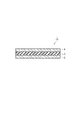
- the photosensitive element 1 according to the present embodiment has a support 2 and a photosensitive layer 3 derived from the photosensitive resin composition formed on the support 2, as shown in FIG. 1 as a schematic cross-sectional view of an example thereof. And other layers such as the protective layer 4 provided as needed.
- polyester films such as polyethylene terephthalate (PET), polybutylene terephthalate (PBT), polyethylene-2,6-naphthalate (PEN), and polyolefin films such as polypropylene and polyethylene.
- PET film may be used because it is easily available and has excellent handleability (particularly, heat resistance, heat shrinkage rate, breaking strength) in the manufacturing process.
- the haze of the support may be 0.01-1.0% or 0.01-0.5%. When the haze is 0.01% or more, the support itself tends to be easy to manufacture, and when it is 1.0% or less, there is a tendency to reduce the minute defects that may occur in the resist pattern. "Haze” means cloudiness.
- the haze in the present disclosure refers to a value measured using a commercially available turbidity meter (turbidity meter) in accordance with the method specified in JIS K7105. The haze can be measured with a commercially available turbidity meter such as NDH-5000 (manufactured by Nippon Denshoku Kogyo Co., Ltd.).
- the thickness of the support may be 1 to 100 ⁇ m, 5 to 60 ⁇ m, 10 to 50 ⁇ m, 10 to 40 ⁇ m, 10 to 30 ⁇ m, or 10 to 25 ⁇ m.
- the thickness of the support is 1 ⁇ m or more, it tends to be possible to prevent the support from being torn when the support is peeled off. Further, when the thickness of the support is 100 ⁇ m or less, it is possible to prevent the resolution from being lowered when exposed through the support.
- the photosensitive element may be further provided with a protective layer, if necessary.
- a protective layer a film may be used in which the adhesive force between the photosensitive layer and the protective layer is smaller than the adhesive force between the photosensitive layer and the support, and a low fisheye film may be used. You may use it. Specifically, for example, those that can be used as the above-mentioned support can be mentioned. From the viewpoint of peelability from the photosensitive layer, a polyethylene film may be used.
- the thickness of the protective layer varies depending on the application, but may be about 1 to 100 ⁇ m.
- the photosensitive element can be manufactured, for example, as follows. That is, a solution (coating liquid) of the photosensitive resin composition is applied onto the support to form a coating layer, and the coating layer is formed by drying the solution. Next, by covering the surface of the photosensitive layer opposite to the support with a protective layer, the support, the photosensitive layer formed on the support, and the protective layer laminated on the photosensitive layer are provided. A photosensitive element is obtained.
- the coating liquid can be applied onto the support by a known method such as roll coating, comma coating, gravure coating, air knife coating, die coating, bar coating and the like.
- Drying of the coating layer is not particularly limited as long as at least a part of the organic solvent can be removed from the coating layer. For example, it may be carried out at 70 to 150 ° C. for about 5 to 30 minutes. After drying, the amount of residual solvent in the photosensitive layer may be 2% by mass or less from the viewpoint of preventing the diffusion of the solvent in a later step.
- the thickness of the photosensitive layer in the photosensitive element can be appropriately selected depending on the intended use, but the thickness after drying may be 1 to 100 ⁇ m, 1 to 50 ⁇ m, or 5 to 40 ⁇ m. When the thickness is 1 ⁇ m or more, industrial coating is facilitated and productivity is improved. Further, when the thickness is 100 ⁇ m or less, the adhesion and the resolution are improved.
- the form of the photosensitive element is not particularly limited.
- it may be in the form of a sheet, or may be in the form of a roll wound around a winding core.
- the support film When winding in a roll shape, the support film may be wound so as to be on the outside.
- the winding core include plastics such as polyethylene resin, polypropylene resin, polystyrene resin, polyvinyl chloride resin, and ABS resin (acrylonitrile-butadiene-styrene copolymer).
- An end face separator may be installed on the end face of the roll-shaped photosensitive element from the viewpoint of end face protection, or a moisture-proof end face separator may be installed from the viewpoint of edge fusion resistance.
- the photosensitive element may be wrapped in a black sheet having low moisture permeability and packaged.
- the photosensitive element can be suitably used, for example, in a method for forming a resist pattern, which will be described later. Above all, from the viewpoint of resolution, it is suitable for application to a manufacturing method for forming a conductor pattern by an etching process.
- the method for forming the resist pattern of the present embodiment is as follows: (i) a step of forming a photosensitive layer on a substrate by using the photosensitive resin composition or the photosensitive element (photosensitive layer forming step). ii) A step (exposure step) of irradiating at least a part (predetermined part) of the photosensitive layer with active light to form a photocurable portion, and (iii) at least a part of the unphotocured portion from the substrate. It may be configured to include a step (development step) for removing the above-mentioned light, and if necessary, other steps.
- the resist pattern can be said to be a photocured product pattern of the photosensitive resin composition, and can also be said to be a relief pattern.
- the method for forming a resist pattern can also be said to be a method for manufacturing a substrate with a resist pattern.
- the photosensitive resin composition may be applied and dried, or after the protective layer is removed from the photosensitive element, the photosensitive layer of the photosensitive element is formed. It may be crimped to the above substrate while heating.
- a photosensitive element it is composed of a substrate, a photosensitive layer, and a support, and a laminated body in which these are laminated in order can be obtained.
- the substrate is not particularly limited, but usually, a circuit forming substrate provided with an insulating layer and a conductor layer formed on the insulating layer, or a die pad (lead frame substrate) such as an alloy substrate is used.
- the photosensitive layer forming step is preferably performed under reduced pressure from the viewpoint of adhesion and followability.
- the photosensitive layer and / or the substrate may be heated at a temperature of 70 to 130 ° C. during crimping.
- the crimping may be performed at a pressure of about 0.1 to 1.0 MPa (about 1 to 10 kgf / cm 2 ), but these conditions are appropriately selected as necessary. If the photosensitive layer is heated to 70 to 130 ° C., it is not necessary to preheat the substrate in advance, but the substrate can be preheated in order to further improve the adhesion and the followability.
- (Ii) exposure step In the exposure step, by irradiating at least a part of the photosensitive layer formed on the substrate with the active light beam, the portion irradiated with the active light ray is photocured to form a latent image.
- the active light can be irradiated through the support if the support is transparent to the active light, but if the support is light-shielding. Irradiates the photosensitive layer with active light rays after removing the support.
- Examples of the exposure method include a method of irradiating an image with active light rays via a negative or positive mask pattern called artwork (mask exposure method). Further, a method of irradiating an active ray in an image shape by a projection exposure method may be adopted. Further, a method of irradiating an active ray in an image shape by a direct drawing exposure method such as an LDI (Laser Direct Imaging) exposure method or a DLP (Digital Light Processing) exposure method may be adopted.
- LDI Laser Direct Imaging
- DLP Digital Light Processing
- a known light source can be used, and for example, a carbon arc lamp, a mercury steam arc lamp, a high-pressure mercury lamp, a xenon lamp, a gas laser such as an argon laser, a solid-state laser such as a YAG laser, a semiconductor laser and the like can be used. Those that effectively radiate ultraviolet rays and visible light are used.
- a resist pattern is formed on the substrate by removing at least a part of the unphotocured portion (other than the photocured portion) of the photosensitive layer from the substrate.
- a support is present on the photosensitive layer, the support is removed, and then the region other than the photocured portion (which can be said to be an unexposed portion) is removed (developed).
- development methods wet development and dry development, and wet development is widely used.
- developer In the case of wet development, develop by a known development method using a developer corresponding to the photosensitive resin composition.
- the developing method include a dip method, a paddle method, a spray method, brushing, slapping, scraping, rocking immersion, and the like, and a high-pressure spray method may be used from the viewpoint of improving resolution. .. Development may be performed by combining these two or more methods.
- the composition of the developer is appropriately selected according to the composition of the photosensitive resin composition.
- the developing solution include an alkaline aqueous solution and an organic solvent developing solution.
- an alkaline aqueous solution may be used as the developer.
- the base of the alkaline aqueous solution include alkali hydroxides such as hydroxides of lithium, sodium or potassium; alkali carbonates such as lithium, sodium, potassium or ammonium carbonates or bicarbonates; potassium phosphates, sodium phosphates and the like.
- Alkaline metal phosphates Alkaline metal phosphates; Alkaline metal pyrophosphates such as sodium pyrophosphate and potassium pyrophosphate; borosand, sodium metasilicate, tetramethylammonium hydroxide, ethanolamine, ethylenediamine, diethylenetriamine, 2-amino-2-hydroxymethyl- 1,3-Propanediol, 1,3-diaminopropanol-2, morpholine and the like are used.
- the alkaline aqueous solution used for development includes a dilute solution of 0.1 to 5% by mass of sodium carbonate, a dilute solution of 0.1 to 5% by mass of potassium carbonate, a dilute solution of 0.1 to 5% by mass of sodium hydroxide, and 0.
- a dilute solution of 1 to 5 mass% sodium tetraborate or the like can be used.
- the pH of the alkaline aqueous solution may be in the range of 9 to 11, and the temperature can be adjusted according to the alkaline developability of the photosensitive layer.
- a surface active agent, a defoaming agent, a small amount of an organic solvent for accelerating development, or the like may be mixed in the alkaline aqueous solution.
- Examples of the organic solvent used in the alkaline aqueous solution include acetone, ethyl acetate, alkoxyethanol having an alkoxy group having 1 to 4 carbon atoms, ethyl alcohol, isopropyl alcohol, butyl alcohol, diethylene glycol monomethyl ether, diethylene glycol monoethyl ether, and diethylene glycol. Examples include monobutyl ether.
- organic solvent used in the organic solvent developer examples include 1,1,1-trichloroethane, N-methylpyrrolidone, N, N-dimethylformamide, cyclohexanone, methyl isobutyl ketone, and ⁇ -butyrolactone.
- water may be added to these organic solvents so as to be in the range of 1 to 20% by mass to prepare an organic solvent developer.
- heating at about 60 to 250 ° C. or exposure of about 0.2 to 10 J / cm 2 is performed as necessary. May include a step of further curing the resist pattern.
- the method for manufacturing a printed wiring board of the present embodiment includes a step of etching or plating a substrate on which a resist pattern is formed by the method for forming a resist pattern to form a conductor pattern, and if necessary, a resist. It may be configured to include other steps such as a pattern removing step.
- the conductor layer provided on the substrate is plated using the resist pattern formed on the substrate as a mask.
- the resist may be removed by removing the resist pattern described later, and the conductor layer covered with the resist may be further etched to form the conductor pattern.
- the method of the plating treatment may be an electrolytic plating treatment, an electroless plating treatment, or an electroless plating treatment.
- the conductor layer provided on the substrate is removed by etching using the resist pattern formed on the substrate as a mask to form the conductor pattern.
- the etching treatment method is appropriately selected according to the conductor layer to be removed.
- the etching solution include a cupric chloride solution, a ferric chloride solution, an alkaline etching solution, and a hydrogen peroxide-based etching solution.
- the resist pattern on the substrate may be removed after the etching treatment or the plating treatment.
- the resist pattern can be removed, for example, with a stronger alkaline aqueous solution than the alkaline aqueous solution used in the development step.
- a stronger alkaline aqueous solution for example, a 1 to 10% by mass sodium hydroxide aqueous solution, a 1 to 10% by mass potassium hydroxide aqueous solution, or the like is used.
- a desired printed wiring board can be manufactured by further etching the conductor layer covered with the resist by the etching treatment to form the conductor pattern.
- the etching treatment method at this time is appropriately selected according to the conductor layer to be removed. For example, the above-mentioned etching solution can be applied.
- the method for manufacturing a printed wiring board according to the present embodiment can be applied not only to the manufacture of a single-layer printed wiring board but also to the manufacture of a multilayer printed wiring board, and also to the manufacture of a printed wiring board having a small-diameter through hole. It is possible.
- Binder polymer Methacrylic acid (MAA), styrene (ST), methyl methacrylate (MMA), butyl methacrylate (BMA), butyl acrylate (BA), as polymerizable monomers for synthesizing the binder polymers used in Examples and Comparative Examples.
- MAA Methacrylic acid
- ST styrene
- MMA methyl methacrylate
- BMA butyl methacrylate
- BA butyl acrylate
- BZMA benzyl methacrylate
- the above solution a was added dropwise to the mixed solution in the flask over 4 hours, and then the mixture was stirred at 80 ° C. for 2 hours. Then, the above solution b was added dropwise to the solution in the flask, and the mixture was stirred at 80 ° C. for 2 hours. Further, the solution in the flask was heated to 95 ° C. over 1 hour while stirring was continued, and then the solution c was added dropwise over 10 minutes and stirred at 95 ° C. for 2 hours to carry out the reaction. After cooling the reaction solution to 50 ° C., methanol was added to obtain a solution of the binder polymer (A-1). The non-volatile content (solid content) of the binder polymer (A-1) was 47.7% by mass.
- Binder Polymers (A-2) to (A-16) The binder polymer (A-2) was obtained in the same manner as in obtaining the solution of the binder polymer (A-1), except that the polymerizable monomer was used in the mass ratio shown in Table 1 or Table 2. )-(A-16) was obtained.
- Weight average molecular weight 120 mg of the binder polymer solution was collected and dissolved in 5 mL of tetrahydrofuran to prepare a sample for Mw measurement. Mw was measured by gel permeation chromatography (GPC) and derived by conversion using a standard polystyrene calibration curve. The conditions of GPC are shown below.
- Glass-transition temperature The glass transition temperature (Tg) of the binder polymer was calculated from the Fox formula.
- Photosensitive resin composition The components (A), (B) and (C) of the blending amount (parts by mass) shown in Table 3 or Table 4 are mixed with 5 parts by mass of methanol, 10 parts by mass of toluene and 11 parts by mass of acetone as solvents. As a result, the photosensitive resin compositions of Examples and Comparative Examples were prepared, respectively.
- the blending amount of the binder polymer shown in Tables 3 and 4 is the mass of the non-volatile component (solid content amount).
- a solution of the photosensitive resin composition is applied onto a polyethylene terephthalate (PET) film (Teijin Film Solution Co., Ltd., trade name "G2J") (support) having a thickness of 16 ⁇ m, and hot air convection drying at 75 ° C and 125 ° C.
- PET polyethylene terephthalate
- G2J trade name
- the film was sequentially dried in a vessel to form a photosensitive layer having a thickness of 25 ⁇ m after drying.
- a polypropylene film (Tamapoli Co., Ltd., product name "NF-13”) (protective layer) is laminated on this photosensitive layer, and the support, the photosensitive layer, and the protective layer are laminated in this order. Obtained.
- the copper surface of the copper-clad laminate was etched to prepare a substrate having eight round holes having a diameter of 200 ⁇ m and a depth of 11 ⁇ m.
- the substrate was heated to 80 ° C., and the photosensitive element was laminated on the substrate.
- Lamination was performed using a heat roll at 110 ° C. at a crimping pressure of 0.3 MPa and a roll speed of 1.5 m / min on the substrate while removing the protective layer. In this way, a laminated body in which the substrate, the photosensitive layer, and the support were laminated in this order was obtained.
- the round hole portion was observed from directly above the laminate using an optical microscope (Keyence Corporation, VK-8500), and the diameter of bubbles generated between the round hole of the substrate and the photosensitive layer was measured. The smaller the diameter of the bubble, the better the followability.
- the photosensitive resin composition containing the binder polymer having a specific structure can form a photosensitive layer having excellent followability.
Landscapes
- Physics & Mathematics (AREA)
- General Physics & Mathematics (AREA)
- Spectroscopy & Molecular Physics (AREA)
- Engineering & Computer Science (AREA)
- Manufacturing & Machinery (AREA)
- Microelectronics & Electronic Packaging (AREA)
- Chemical & Material Sciences (AREA)
- Chemical Kinetics & Catalysis (AREA)
- Materials For Photolithography (AREA)
- Manufacturing Of Printed Circuit Boards (AREA)
- Exposure And Positioning Against Photoresist Photosensitive Materials (AREA)
- Polymerisation Methods In General (AREA)
- Manufacturing Of Printed Wiring (AREA)
Priority Applications (8)
| Application Number | Priority Date | Filing Date | Title |
|---|---|---|---|
| PCT/JP2020/043605 WO2022113161A1 (ja) | 2020-11-24 | 2020-11-24 | 感光性樹脂組成物、感光性エレメント、レジストパターンの形成方法及びプリント配線板の製造方法 |
| JP2022562370A JP7425982B2 (ja) | 2020-11-24 | 2021-11-16 | 感光性樹脂組成物、感光性エレメント、レジストパターンの形成方法及びプリント配線板の製造方法 |
| PCT/JP2021/042092 WO2022113829A1 (ja) | 2020-11-24 | 2021-11-16 | 感光性樹脂組成物、感光性エレメント、レジストパターンの形成方法及びプリント配線板の製造方法 |
| KR1020237019362A KR102895226B1 (ko) | 2020-11-24 | 2021-11-16 | 감광성 수지 조성물, 감광성 엘리먼트, 레지스트 패턴의 형성 방법 및 프린트 배선판의 제조 방법 |
| CN202180007845.1A CN114902137A (zh) | 2020-11-24 | 2021-11-16 | 感光性树脂组合物、感光性元件、抗蚀剂图案的形成方法及印刷线路板的制造方法 |
| CN202210896651.8A CN115167077A (zh) | 2020-11-24 | 2021-11-16 | 感光性树脂组合物、感光性元件、抗蚀剂图案的形成方法及印刷线路板的制造方法 |
| TW110142698A TWI877430B (zh) | 2020-11-24 | 2021-11-17 | 感光性樹脂組成物、感光性元件、抗蝕劑圖案之形成方法及印刷配線板之製造方法 |
| JP2023179342A JP2024008940A (ja) | 2020-11-24 | 2023-10-18 | 感光性樹脂組成物、感光性エレメント、レジストパターンの形成方法及びプリント配線板の製造方法 |
Applications Claiming Priority (1)
| Application Number | Priority Date | Filing Date | Title |
|---|---|---|---|
| PCT/JP2020/043605 WO2022113161A1 (ja) | 2020-11-24 | 2020-11-24 | 感光性樹脂組成物、感光性エレメント、レジストパターンの形成方法及びプリント配線板の製造方法 |
Publications (1)
| Publication Number | Publication Date |
|---|---|
| WO2022113161A1 true WO2022113161A1 (ja) | 2022-06-02 |
Family
ID=81754092
Family Applications (2)
| Application Number | Title | Priority Date | Filing Date |
|---|---|---|---|
| PCT/JP2020/043605 Ceased WO2022113161A1 (ja) | 2020-11-24 | 2020-11-24 | 感光性樹脂組成物、感光性エレメント、レジストパターンの形成方法及びプリント配線板の製造方法 |
| PCT/JP2021/042092 Ceased WO2022113829A1 (ja) | 2020-11-24 | 2021-11-16 | 感光性樹脂組成物、感光性エレメント、レジストパターンの形成方法及びプリント配線板の製造方法 |
Family Applications After (1)
| Application Number | Title | Priority Date | Filing Date |
|---|---|---|---|
| PCT/JP2021/042092 Ceased WO2022113829A1 (ja) | 2020-11-24 | 2021-11-16 | 感光性樹脂組成物、感光性エレメント、レジストパターンの形成方法及びプリント配線板の製造方法 |
Country Status (5)
| Country | Link |
|---|---|
| JP (2) | JP7425982B2 (https=) |
| KR (1) | KR102895226B1 (https=) |
| CN (2) | CN114902137A (https=) |
| TW (1) | TWI877430B (https=) |
| WO (2) | WO2022113161A1 (https=) |
Families Citing this family (2)
| Publication number | Priority date | Publication date | Assignee | Title |
|---|---|---|---|---|
| WO2024210041A1 (ja) * | 2023-04-03 | 2024-10-10 | 株式会社レゾナック | 感光性樹脂組成物、感光性エレメント、レジストパターンの形成方法及び配線基板の製造方法 |
| JP2025155987A (ja) * | 2024-03-29 | 2025-10-14 | 旭化成株式会社 | 感光性樹脂積層体、及びその製造方法 |
Citations (4)
| Publication number | Priority date | Publication date | Assignee | Title |
|---|---|---|---|---|
| JPH03236956A (ja) * | 1989-05-17 | 1991-10-22 | Asahi Chem Ind Co Ltd | 光硬化性樹脂積層体及びそれを用いるプリント配線板の製造方法 |
| JP2010020264A (ja) * | 2007-08-09 | 2010-01-28 | Nichigo Morton Co Ltd | ソルダーレジストフィルム、レジストパターン形成方法および発光装置 |
| WO2013141286A1 (ja) * | 2012-03-23 | 2013-09-26 | 日立化成株式会社 | 感光性樹脂組成物、及びこれを用いた加工ガラス基板の製造方法、並びにタッチパネル及びその製造方法 |
| JP2017129736A (ja) * | 2016-01-20 | 2017-07-27 | 互応化学工業株式会社 | 感光性樹脂組成物、ドライフィルム、プリント配線板、及び感光性樹脂組成物の製造方法 |
Family Cites Families (15)
| Publication number | Priority date | Publication date | Assignee | Title |
|---|---|---|---|---|
| JP4461037B2 (ja) * | 2005-02-09 | 2010-05-12 | ニチゴー・モートン株式会社 | 感光性樹脂組成物およびそれを用いてなる感光性樹脂積層体 |
| JP4646759B2 (ja) * | 2005-09-20 | 2011-03-09 | 旭化成イーマテリアルズ株式会社 | パターン形成材料、並びにパターン形成装置及びパターン形成方法 |
| JP2009003000A (ja) * | 2007-06-19 | 2009-01-08 | Hitachi Chem Co Ltd | 感光性樹脂組成物、これを用いた感光性エレメント、レジストパターンの形成方法、プリント配線板の製造方法及び光硬化物の除去方法 |
| JP4924230B2 (ja) | 2007-06-21 | 2012-04-25 | 日立化成工業株式会社 | 感光性樹脂組成物、これを用いた感光性エレメント、レジストパターンの形成方法及びプリント配線板の製造方法 |
| JP4935833B2 (ja) * | 2009-01-23 | 2012-05-23 | 日立化成工業株式会社 | 感光性樹脂組成物、これを用いた感光性エレメント、画像表示装置の隔壁の形成方法及び画像表示装置の製造方法 |
| JP2010249884A (ja) * | 2009-04-10 | 2010-11-04 | Dupont Mrc Dryfilm Ltd | 光重合性樹脂組成物およびこれを用いた感光性フィルム |
| JP5777461B2 (ja) | 2011-09-14 | 2015-09-09 | 旭化成イーマテリアルズ株式会社 | 感光性樹脂組成物 |
| JP5853588B2 (ja) * | 2011-10-26 | 2016-02-09 | 日立化成株式会社 | 感光性樹脂組成物、感光性エレメント、レジストパターンの形成方法及びプリント配線板の製造方法 |
| US10104781B2 (en) * | 2013-12-27 | 2018-10-16 | Hitachi Chemical Company, Ltd. | Photosensitive resin composition, photosensitive element, method for forming resist pattern, and method for producing printed wiring board |
| CN105629662B (zh) * | 2015-12-31 | 2019-09-10 | 杭州福斯特应用材料股份有限公司 | 一种干膜光致抗蚀剂 |
| JP2017191171A (ja) * | 2016-04-12 | 2017-10-19 | 日立化成株式会社 | 感光性樹脂組成物、感光性エレメント、レジストパターンの形成方法及びプリント配線板の製造方法 |
| WO2019088268A1 (ja) * | 2017-11-06 | 2019-05-09 | 旭化成株式会社 | 感光性樹脂積層体及びレジストパターンの製造方法 |
| CN108241259B (zh) * | 2018-01-24 | 2021-08-10 | 杭州福斯特电子材料有限公司 | 一种具有良好孔掩蔽功能可直接描绘曝光成像的抗蚀剂组合物 |
| TWI882983B (zh) * | 2019-02-05 | 2025-05-11 | 日商力森諾科股份有限公司 | 感光性樹脂組成物、感光性元件、阻劑圖案的形成方法及印刷線路板的製造方法 |
| CN111965939B (zh) * | 2020-08-11 | 2023-06-20 | 杭州福斯特电子材料有限公司 | 一种感光树脂组合物及其干膜抗蚀剂 |
-
2020
- 2020-11-24 WO PCT/JP2020/043605 patent/WO2022113161A1/ja not_active Ceased
-
2021
- 2021-11-16 CN CN202180007845.1A patent/CN114902137A/zh active Pending
- 2021-11-16 JP JP2022562370A patent/JP7425982B2/ja active Active
- 2021-11-16 KR KR1020237019362A patent/KR102895226B1/ko active Active
- 2021-11-16 WO PCT/JP2021/042092 patent/WO2022113829A1/ja not_active Ceased
- 2021-11-16 CN CN202210896651.8A patent/CN115167077A/zh active Pending
- 2021-11-17 TW TW110142698A patent/TWI877430B/zh active
-
2023
- 2023-10-18 JP JP2023179342A patent/JP2024008940A/ja active Pending
Patent Citations (4)
| Publication number | Priority date | Publication date | Assignee | Title |
|---|---|---|---|---|
| JPH03236956A (ja) * | 1989-05-17 | 1991-10-22 | Asahi Chem Ind Co Ltd | 光硬化性樹脂積層体及びそれを用いるプリント配線板の製造方法 |
| JP2010020264A (ja) * | 2007-08-09 | 2010-01-28 | Nichigo Morton Co Ltd | ソルダーレジストフィルム、レジストパターン形成方法および発光装置 |
| WO2013141286A1 (ja) * | 2012-03-23 | 2013-09-26 | 日立化成株式会社 | 感光性樹脂組成物、及びこれを用いた加工ガラス基板の製造方法、並びにタッチパネル及びその製造方法 |
| JP2017129736A (ja) * | 2016-01-20 | 2017-07-27 | 互応化学工業株式会社 | 感光性樹脂組成物、ドライフィルム、プリント配線板、及び感光性樹脂組成物の製造方法 |
Also Published As
| Publication number | Publication date |
|---|---|
| KR102895226B1 (ko) | 2025-12-04 |
| CN114902137A (zh) | 2022-08-12 |
| CN115167077A (zh) | 2022-10-11 |
| JP2024008940A (ja) | 2024-01-19 |
| TW202227577A (zh) | 2022-07-16 |
| JPWO2022113829A1 (https=) | 2022-06-02 |
| JP7425982B2 (ja) | 2024-02-01 |
| WO2022113829A1 (ja) | 2022-06-02 |
| KR20230109152A (ko) | 2023-07-19 |
| TWI877430B (zh) | 2025-03-21 |
Similar Documents
| Publication | Publication Date | Title |
|---|---|---|
| JP5327310B2 (ja) | 感光性樹脂組成物、並びにこれを用いた感光性エレメント、レジストパターンの形成方法及びプリント配線板の製造方法 | |
| US9989854B2 (en) | Photosensitive resin composition for projection exposure, photosensitive element, method for forming resist pattern, process for producing printed wiring board and process for producing lead frame | |
| JP5626428B2 (ja) | 感光性樹脂組成物、並びにこれを用いた感光性エレメント、レジストパターンの形成方法及びプリント配線板の製造方法 | |
| JPWO2008078483A1 (ja) | 感光性樹脂組成物、感光性エレメント、レジストパターンの形成方法及びプリント配線板の製造方法 | |
| JP2009003000A (ja) | 感光性樹脂組成物、これを用いた感光性エレメント、レジストパターンの形成方法、プリント配線板の製造方法及び光硬化物の除去方法 | |
| JP6690532B2 (ja) | 感光性樹脂組成物、感光性エレメント、レジストパターンの形成方法及びプリント配線板の製造方法 | |
| JP5600903B2 (ja) | 感光性樹脂組成物、並びにこれを用いた感光性エレメント、レジストパターンの形成方法及びプリント配線板の製造方法 | |
| WO2009154194A1 (ja) | 感光性樹脂組成物、並びにこれを用いた感光性エレメント、レジストパターンの形成方法及びプリント配線板の製造法 | |
| JP2024008940A (ja) | 感光性樹脂組成物、感光性エレメント、レジストパターンの形成方法及びプリント配線板の製造方法 | |
| JP7507862B2 (ja) | アルカリ可溶性樹脂、感光性樹脂組成物、感光性エレメント、レジストパターンの形成方法、及び配線パターンの形成方法 | |
| JP5532551B2 (ja) | 感光性樹脂組成物、感光性エレメント、レジストパターンの形成方法及びプリント配線板の製造方法 | |
| JP7631907B2 (ja) | 感光性樹脂フィルム、感光性エレメント、及び、積層体の製造方法 | |
| JP2024003098A (ja) | 感光性樹脂フィルム、レジストパターンの形成方法、及び配線パターンの形成方法 | |
| JP2010060891A (ja) | 感光性樹脂組成物、これを用いた感光性エレメント、レジストパターンの形成方法及びプリント配線板の製造方法 | |
| JP7327485B2 (ja) | 感光性樹脂組成物、感光性エレメント、レジストパターンの形成方法及びプリント配線板の製造方法 | |
| WO2023050062A1 (en) | Polymer, photosensitive resin composition, photosensitive element, method for forming resist pattern, and method for forming wiring pattern | |
| WO2022201432A1 (ja) | 感光性樹脂フィルム、レジストパターンの形成方法、及び配線パターンの形成方法 | |
| JP2013122488A (ja) | 感光性樹脂組成物、これを用いた感光性エレメント、レジストパターンの形成方法及びプリント配線板の製造方法 |
Legal Events
| Date | Code | Title | Description |
|---|---|---|---|
| 121 | Ep: the epo has been informed by wipo that ep was designated in this application |
Ref document number: 20963426 Country of ref document: EP Kind code of ref document: A1 |
|
| NENP | Non-entry into the national phase |
Ref country code: DE |
|
| 122 | Ep: pct application non-entry in european phase |
Ref document number: 20963426 Country of ref document: EP Kind code of ref document: A1 |
|
| NENP | Non-entry into the national phase |
Ref country code: JP |