WO2022044541A1 - 半導体装置 - Google Patents
半導体装置 Download PDFInfo
- Publication number
- WO2022044541A1 WO2022044541A1 PCT/JP2021/024996 JP2021024996W WO2022044541A1 WO 2022044541 A1 WO2022044541 A1 WO 2022044541A1 JP 2021024996 W JP2021024996 W JP 2021024996W WO 2022044541 A1 WO2022044541 A1 WO 2022044541A1
- Authority
- WO
- WIPO (PCT)
- Prior art keywords
- circuit pattern
- circuit
- semiconductor device
- resin layer
- front surface
- Prior art date
- Legal status (The legal status is an assumption and is not a legal conclusion. Google has not performed a legal analysis and makes no representation as to the accuracy of the status listed.)
- Ceased
Links
Images





Classifications
-
- H—ELECTRICITY
- H10—SEMICONDUCTOR DEVICES; ELECTRIC SOLID-STATE DEVICES NOT OTHERWISE PROVIDED FOR
- H10W—GENERIC PACKAGES, INTERCONNECTIONS, CONNECTORS OR OTHER CONSTRUCTIONAL DETAILS OF DEVICES COVERED BY CLASS H10
- H10W40/00—Arrangements for thermal protection or thermal control
- H10W40/20—Arrangements for cooling
- H10W40/22—Arrangements for cooling characterised by their shape, e.g. having conical or cylindrical projections
-
- H—ELECTRICITY
- H10—SEMICONDUCTOR DEVICES; ELECTRIC SOLID-STATE DEVICES NOT OTHERWISE PROVIDED FOR
- H10W—GENERIC PACKAGES, INTERCONNECTIONS, CONNECTORS OR OTHER CONSTRUCTIONAL DETAILS OF DEVICES COVERED BY CLASS H10
- H10W70/00—Package substrates; Interposers; Redistribution layers [RDL]
- H10W70/60—Insulating or insulated package substrates; Interposers; Redistribution layers
- H10W70/62—Insulating or insulated package substrates; Interposers; Redistribution layers characterised by their interconnections
- H10W70/65—Shapes or dispositions of interconnections
-
- H—ELECTRICITY
- H10—SEMICONDUCTOR DEVICES; ELECTRIC SOLID-STATE DEVICES NOT OTHERWISE PROVIDED FOR
- H10W—GENERIC PACKAGES, INTERCONNECTIONS, CONNECTORS OR OTHER CONSTRUCTIONAL DETAILS OF DEVICES COVERED BY CLASS H10
- H10W40/00—Arrangements for thermal protection or thermal control
- H10W40/10—Arrangements for heating
-
- H—ELECTRICITY
- H10—SEMICONDUCTOR DEVICES; ELECTRIC SOLID-STATE DEVICES NOT OTHERWISE PROVIDED FOR
- H10W—GENERIC PACKAGES, INTERCONNECTIONS, CONNECTORS OR OTHER CONSTRUCTIONAL DETAILS OF DEVICES COVERED BY CLASS H10
- H10W70/00—Package substrates; Interposers; Redistribution layers [RDL]
- H10W70/60—Insulating or insulated package substrates; Interposers; Redistribution layers
- H10W70/611—Insulating or insulated package substrates; Interposers; Redistribution layers for connecting multiple chips together
-
- H—ELECTRICITY
- H10—SEMICONDUCTOR DEVICES; ELECTRIC SOLID-STATE DEVICES NOT OTHERWISE PROVIDED FOR
- H10W—GENERIC PACKAGES, INTERCONNECTIONS, CONNECTORS OR OTHER CONSTRUCTIONAL DETAILS OF DEVICES COVERED BY CLASS H10
- H10W70/00—Package substrates; Interposers; Redistribution layers [RDL]
- H10W70/60—Insulating or insulated package substrates; Interposers; Redistribution layers
- H10W70/67—Insulating or insulated package substrates; Interposers; Redistribution layers characterised by their insulating layers or insulating parts
- H10W70/68—Shapes or dispositions thereof
- H10W70/6875—Shapes or dispositions thereof being on a metallic substrate, e.g. insulated metal substrates [IMS]
-
- H—ELECTRICITY
- H10—SEMICONDUCTOR DEVICES; ELECTRIC SOLID-STATE DEVICES NOT OTHERWISE PROVIDED FOR
- H10W—GENERIC PACKAGES, INTERCONNECTIONS, CONNECTORS OR OTHER CONSTRUCTIONAL DETAILS OF DEVICES COVERED BY CLASS H10
- H10W76/00—Containers; Fillings or auxiliary members therefor; Seals
- H10W76/10—Containers or parts thereof
- H10W76/12—Containers or parts thereof characterised by their shape
- H10W76/15—Containers comprising an insulating or insulated base
- H10W76/157—Containers comprising an insulating or insulated base having interconnections parallel to the insulating or insulated base
-
- H—ELECTRICITY
- H10—SEMICONDUCTOR DEVICES; ELECTRIC SOLID-STATE DEVICES NOT OTHERWISE PROVIDED FOR
- H10W—GENERIC PACKAGES, INTERCONNECTIONS, CONNECTORS OR OTHER CONSTRUCTIONAL DETAILS OF DEVICES COVERED BY CLASS H10
- H10W76/00—Containers; Fillings or auxiliary members therefor; Seals
- H10W76/40—Fillings or auxiliary members in containers, e.g. centering rings
- H10W76/42—Fillings
- H10W76/47—Solid or gel fillings
-
- H—ELECTRICITY
- H10—SEMICONDUCTOR DEVICES; ELECTRIC SOLID-STATE DEVICES NOT OTHERWISE PROVIDED FOR
- H10W—GENERIC PACKAGES, INTERCONNECTIONS, CONNECTORS OR OTHER CONSTRUCTIONAL DETAILS OF DEVICES COVERED BY CLASS H10
- H10W40/00—Arrangements for thermal protection or thermal control
- H10W40/20—Arrangements for cooling
- H10W40/25—Arrangements for cooling characterised by their materials
- H10W40/255—Arrangements for cooling characterised by their materials having a laminate or multilayered structure, e.g. direct bond copper [DBC] ceramic substrates
-
- H—ELECTRICITY
- H10—SEMICONDUCTOR DEVICES; ELECTRIC SOLID-STATE DEVICES NOT OTHERWISE PROVIDED FOR
- H10W—GENERIC PACKAGES, INTERCONNECTIONS, CONNECTORS OR OTHER CONSTRUCTIONAL DETAILS OF DEVICES COVERED BY CLASS H10
- H10W72/00—Interconnections or connectors in packages
- H10W72/071—Connecting or disconnecting
- H10W72/073—Connecting or disconnecting of die-attach connectors
- H10W72/07331—Connecting techniques
- H10W72/07336—Soldering or alloying
-
- H—ELECTRICITY
- H10—SEMICONDUCTOR DEVICES; ELECTRIC SOLID-STATE DEVICES NOT OTHERWISE PROVIDED FOR
- H10W—GENERIC PACKAGES, INTERCONNECTIONS, CONNECTORS OR OTHER CONSTRUCTIONAL DETAILS OF DEVICES COVERED BY CLASS H10
- H10W72/00—Interconnections or connectors in packages
- H10W72/071—Connecting or disconnecting
- H10W72/075—Connecting or disconnecting of bond wires
-
- H—ELECTRICITY
- H10—SEMICONDUCTOR DEVICES; ELECTRIC SOLID-STATE DEVICES NOT OTHERWISE PROVIDED FOR
- H10W—GENERIC PACKAGES, INTERCONNECTIONS, CONNECTORS OR OTHER CONSTRUCTIONAL DETAILS OF DEVICES COVERED BY CLASS H10
- H10W72/00—Interconnections or connectors in packages
- H10W72/071—Connecting or disconnecting
- H10W72/075—Connecting or disconnecting of bond wires
- H10W72/07551—Connecting or disconnecting of bond wires characterised by changes in properties of the bond wires during the connecting
- H10W72/07554—Connecting or disconnecting of bond wires characterised by changes in properties of the bond wires during the connecting changes in dispositions
-
- H—ELECTRICITY
- H10—SEMICONDUCTOR DEVICES; ELECTRIC SOLID-STATE DEVICES NOT OTHERWISE PROVIDED FOR
- H10W—GENERIC PACKAGES, INTERCONNECTIONS, CONNECTORS OR OTHER CONSTRUCTIONAL DETAILS OF DEVICES COVERED BY CLASS H10
- H10W72/00—Interconnections or connectors in packages
- H10W72/30—Die-attach connectors
-
- H—ELECTRICITY
- H10—SEMICONDUCTOR DEVICES; ELECTRIC SOLID-STATE DEVICES NOT OTHERWISE PROVIDED FOR
- H10W—GENERIC PACKAGES, INTERCONNECTIONS, CONNECTORS OR OTHER CONSTRUCTIONAL DETAILS OF DEVICES COVERED BY CLASS H10
- H10W72/00—Interconnections or connectors in packages
- H10W72/30—Die-attach connectors
- H10W72/351—Materials of die-attach connectors
- H10W72/352—Materials of die-attach connectors comprising metals or metalloids, e.g. solders
-
- H—ELECTRICITY
- H10—SEMICONDUCTOR DEVICES; ELECTRIC SOLID-STATE DEVICES NOT OTHERWISE PROVIDED FOR
- H10W—GENERIC PACKAGES, INTERCONNECTIONS, CONNECTORS OR OTHER CONSTRUCTIONAL DETAILS OF DEVICES COVERED BY CLASS H10
- H10W72/00—Interconnections or connectors in packages
- H10W72/50—Bond wires
- H10W72/541—Dispositions of bond wires
- H10W72/547—Dispositions of multiple bond wires
-
- H—ELECTRICITY
- H10—SEMICONDUCTOR DEVICES; ELECTRIC SOLID-STATE DEVICES NOT OTHERWISE PROVIDED FOR
- H10W—GENERIC PACKAGES, INTERCONNECTIONS, CONNECTORS OR OTHER CONSTRUCTIONAL DETAILS OF DEVICES COVERED BY CLASS H10
- H10W72/00—Interconnections or connectors in packages
- H10W72/50—Bond wires
- H10W72/541—Dispositions of bond wires
- H10W72/547—Dispositions of multiple bond wires
- H10W72/5473—Dispositions of multiple bond wires multiple bond wires connected to a common bond pad
-
- H—ELECTRICITY
- H10—SEMICONDUCTOR DEVICES; ELECTRIC SOLID-STATE DEVICES NOT OTHERWISE PROVIDED FOR
- H10W—GENERIC PACKAGES, INTERCONNECTIONS, CONNECTORS OR OTHER CONSTRUCTIONAL DETAILS OF DEVICES COVERED BY CLASS H10
- H10W72/00—Interconnections or connectors in packages
- H10W72/50—Bond wires
- H10W72/541—Dispositions of bond wires
- H10W72/547—Dispositions of multiple bond wires
- H10W72/5475—Dispositions of multiple bond wires multiple bond wires connected to common bond pads at both ends of the wires
-
- H—ELECTRICITY
- H10—SEMICONDUCTOR DEVICES; ELECTRIC SOLID-STATE DEVICES NOT OTHERWISE PROVIDED FOR
- H10W—GENERIC PACKAGES, INTERCONNECTIONS, CONNECTORS OR OTHER CONSTRUCTIONAL DETAILS OF DEVICES COVERED BY CLASS H10
- H10W72/00—Interconnections or connectors in packages
- H10W72/50—Bond wires
- H10W72/551—Materials of bond wires
- H10W72/552—Materials of bond wires comprising metals or metalloids, e.g. silver
-
- H—ELECTRICITY
- H10—SEMICONDUCTOR DEVICES; ELECTRIC SOLID-STATE DEVICES NOT OTHERWISE PROVIDED FOR
- H10W—GENERIC PACKAGES, INTERCONNECTIONS, CONNECTORS OR OTHER CONSTRUCTIONAL DETAILS OF DEVICES COVERED BY CLASS H10
- H10W72/00—Interconnections or connectors in packages
- H10W72/50—Bond wires
- H10W72/551—Materials of bond wires
- H10W72/552—Materials of bond wires comprising metals or metalloids, e.g. silver
- H10W72/5522—Materials of bond wires comprising metals or metalloids, e.g. silver comprising gold [Au]
-
- H—ELECTRICITY
- H10—SEMICONDUCTOR DEVICES; ELECTRIC SOLID-STATE DEVICES NOT OTHERWISE PROVIDED FOR
- H10W—GENERIC PACKAGES, INTERCONNECTIONS, CONNECTORS OR OTHER CONSTRUCTIONAL DETAILS OF DEVICES COVERED BY CLASS H10
- H10W72/00—Interconnections or connectors in packages
- H10W72/50—Bond wires
- H10W72/551—Materials of bond wires
- H10W72/552—Materials of bond wires comprising metals or metalloids, e.g. silver
- H10W72/5524—Materials of bond wires comprising metals or metalloids, e.g. silver comprising aluminium [Al]
-
- H—ELECTRICITY
- H10—SEMICONDUCTOR DEVICES; ELECTRIC SOLID-STATE DEVICES NOT OTHERWISE PROVIDED FOR
- H10W—GENERIC PACKAGES, INTERCONNECTIONS, CONNECTORS OR OTHER CONSTRUCTIONAL DETAILS OF DEVICES COVERED BY CLASS H10
- H10W72/00—Interconnections or connectors in packages
- H10W72/50—Bond wires
- H10W72/551—Materials of bond wires
- H10W72/552—Materials of bond wires comprising metals or metalloids, e.g. silver
- H10W72/5525—Materials of bond wires comprising metals or metalloids, e.g. silver comprising copper [Cu]
-
- H—ELECTRICITY
- H10—SEMICONDUCTOR DEVICES; ELECTRIC SOLID-STATE DEVICES NOT OTHERWISE PROVIDED FOR
- H10W—GENERIC PACKAGES, INTERCONNECTIONS, CONNECTORS OR OTHER CONSTRUCTIONAL DETAILS OF DEVICES COVERED BY CLASS H10
- H10W72/00—Interconnections or connectors in packages
- H10W72/50—Bond wires
- H10W72/59—Bond pads specially adapted therefor
-
- H—ELECTRICITY
- H10—SEMICONDUCTOR DEVICES; ELECTRIC SOLID-STATE DEVICES NOT OTHERWISE PROVIDED FOR
- H10W—GENERIC PACKAGES, INTERCONNECTIONS, CONNECTORS OR OTHER CONSTRUCTIONAL DETAILS OF DEVICES COVERED BY CLASS H10
- H10W72/00—Interconnections or connectors in packages
- H10W72/851—Dispositions of multiple connectors or interconnections
- H10W72/874—On different surfaces
- H10W72/884—Die-attach connectors and bond wires
-
- H—ELECTRICITY
- H10—SEMICONDUCTOR DEVICES; ELECTRIC SOLID-STATE DEVICES NOT OTHERWISE PROVIDED FOR
- H10W—GENERIC PACKAGES, INTERCONNECTIONS, CONNECTORS OR OTHER CONSTRUCTIONAL DETAILS OF DEVICES COVERED BY CLASS H10
- H10W72/00—Interconnections or connectors in packages
- H10W72/90—Bond pads, in general
- H10W72/921—Structures or relative sizes of bond pads
- H10W72/926—Multiple bond pads having different sizes
-
- H—ELECTRICITY
- H10—SEMICONDUCTOR DEVICES; ELECTRIC SOLID-STATE DEVICES NOT OTHERWISE PROVIDED FOR
- H10W—GENERIC PACKAGES, INTERCONNECTIONS, CONNECTORS OR OTHER CONSTRUCTIONAL DETAILS OF DEVICES COVERED BY CLASS H10
- H10W72/00—Interconnections or connectors in packages
- H10W72/90—Bond pads, in general
- H10W72/951—Materials of bond pads
- H10W72/952—Materials of bond pads comprising metals or metalloids, e.g. PbSn, Ag or Cu
-
- H—ELECTRICITY
- H10—SEMICONDUCTOR DEVICES; ELECTRIC SOLID-STATE DEVICES NOT OTHERWISE PROVIDED FOR
- H10W—GENERIC PACKAGES, INTERCONNECTIONS, CONNECTORS OR OTHER CONSTRUCTIONAL DETAILS OF DEVICES COVERED BY CLASS H10
- H10W74/00—Encapsulations, e.g. protective coatings
-
- H—ELECTRICITY
- H10—SEMICONDUCTOR DEVICES; ELECTRIC SOLID-STATE DEVICES NOT OTHERWISE PROVIDED FOR
- H10W—GENERIC PACKAGES, INTERCONNECTIONS, CONNECTORS OR OTHER CONSTRUCTIONAL DETAILS OF DEVICES COVERED BY CLASS H10
- H10W90/00—Package configurations
-
- H—ELECTRICITY
- H10—SEMICONDUCTOR DEVICES; ELECTRIC SOLID-STATE DEVICES NOT OTHERWISE PROVIDED FOR
- H10W—GENERIC PACKAGES, INTERCONNECTIONS, CONNECTORS OR OTHER CONSTRUCTIONAL DETAILS OF DEVICES COVERED BY CLASS H10
- H10W90/00—Package configurations
- H10W90/701—Package configurations characterised by the relative positions of pads or connectors relative to package parts
- H10W90/751—Package configurations characterised by the relative positions of pads or connectors relative to package parts of bond wires
- H10W90/753—Package configurations characterised by the relative positions of pads or connectors relative to package parts of bond wires between laterally-adjacent chips
-
- H—ELECTRICITY
- H10—SEMICONDUCTOR DEVICES; ELECTRIC SOLID-STATE DEVICES NOT OTHERWISE PROVIDED FOR
- H10W—GENERIC PACKAGES, INTERCONNECTIONS, CONNECTORS OR OTHER CONSTRUCTIONAL DETAILS OF DEVICES COVERED BY CLASS H10
- H10W90/00—Package configurations
- H10W90/701—Package configurations characterised by the relative positions of pads or connectors relative to package parts
- H10W90/751—Package configurations characterised by the relative positions of pads or connectors relative to package parts of bond wires
- H10W90/754—Package configurations characterised by the relative positions of pads or connectors relative to package parts of bond wires between a chip and a stacked insulating package substrate, interposer or RDL
Definitions
- the present invention relates to a semiconductor device.
- the semiconductor devices include power devices.
- the power device is, for example, a semiconductor chip including an IGBT (Insulated Gate Bipolar Transistor) and a power MOSFET (Metal Oxide Semiconductor Field Effect Transistor).
- the semiconductor device includes an insulating circuit board on which the above-mentioned semiconductor chip is arranged.
- the insulating circuit board includes a ceramic plate, a circuit pattern formed on the front surface of the ceramic plate, and a metal plate formed on the back surface of the ceramic plate.
- the semiconductor chip is joined on the circuit pattern.
- the case is bonded to the insulating circuit board by an adhesive so as to surround the outer peripheral end portion of the insulating circuit board.
- the case is insert-molded with lead frames for input and output. In the case, the semiconductor chip and the lead frame are electrically connected by wires (see, for example, Patent Document 1).
- the insulated circuit board is greatly warped due to the heat generated by the semiconductor chip. Further, if the insulating circuit board is repeatedly warped due to the heat cycle of the semiconductor device, cracks may occur in the ceramic plate, and the generated cracks may further extend. When the ceramic plate is damaged in this way, the thermal conductivity and the insulating property of the insulating circuit board are lowered, and the long-term reliability of the semiconductor device is lowered.
- the present invention has been made in view of such a point, and an object of the present invention is to provide a semiconductor device in which the occurrence of warpage due to heat is reduced.
- an insulating circuit board including a base plate, a resin layer formed on the front surface of the base plate, and a circuit pattern formed on the resin front surface of the resin layer.
- the circuit front surface of the circuit pattern includes a semiconductor chip having a rectangular shape in a plan view, in which a side end portion is joined to the circuit front surface of the circuit pattern at a distance of a predetermined distance or more from the outer peripheral end portion.
- a semiconductor device is provided in which the predetermined distance and the thickness of the circuit pattern are each 0.1 times or more the length of one side of the semiconductor chip.
- FIG. 2 is a cross-sectional view of a main part of the semiconductor device according to the fourth embodiment (No. 2). It is sectional drawing of the main part of the semiconductor device of 5th Embodiment.
- the "front surface” and the “upper surface” represent the surface facing upward in the semiconductor device 10 of FIG. Similarly, “upper” refers to the upper direction in the semiconductor device 10 of FIG.
- the “back surface” and the “bottom surface” represent a surface facing downward in the semiconductor device 10 of FIG. Similarly, “bottom” represents the direction of the lower side in the semiconductor device 10 of FIG.
- Other drawings mean the same direction as needed.
- the "front surface”, “upper surface”, “upper”, “back surface”, “lower surface”, “lower”, and “side surface” are merely expedient expressions for specifying the relative positional relationship, and are the present invention. It does not limit the technical idea of.
- top and bottom do not necessarily mean vertical to the ground. That is, the “up” and “down” directions are not limited to the direction of gravity. Further, in the following description, the "principal component” means a case containing 80 vol% or more.
- FIG. 1 is a diagram for explaining the semiconductor device of the first embodiment.
- FIG. 1A is an enlarged view of a main part of the semiconductor device 1 in a plan view.
- 1 (B) is a cross-sectional view taken along the alternate long and short dash line XX of FIG. 1 (A).
- the semiconductor device 1 includes an insulating circuit board 2 and semiconductor chips 6a and 6b.
- the insulating circuit board 2 includes a circuit pattern 3, a resin layer 4 having a circuit pattern 3 formed on a front surface (resin front surface), and a base plate 5 having a resin layer 4 formed on the front surface. There is.
- the circuit pattern 3 and the base plate 5 are made of a conductive metal.
- the resin layer 4 is made of a resin having low thermal resistance and high insulating properties.
- the semiconductor chips 6a and 6b are power devices having a rectangular shape in a plan view. The semiconductor chips 6a and 6b are joined to the front surface (circuit front surface) of the circuit pattern 3.
- the semiconductor chips 6a and 6b are joined so that the side ends of the circuit pattern 3 are separated from the outer peripheral end of the circuit pattern 3 by a predetermined distance D1 or more and are separated from the inside of the circuit pattern 3.
- the predetermined distance D1 corresponds to the thickness T of the circuit pattern 3.
- the thickness T of the circuit pattern 3 is 0.1 times or more the length of one side of the semiconductor chips 6a and 6b. That is, the predetermined distance D1 and the thickness T of the circuit pattern 3 are both 0.1 times or more the length of one side of the semiconductor chips 6a and 6b.
- the gap D2 between the side ends facing each other in the side view of the semiconductor chips 6a and 6b is more than twice the predetermined distance D1.
- the gap D2 between the side ends facing each other in the side view of the semiconductor chips 6a and 6b is 0.2 times or more the length of one side of the semiconductor chips 6a and 6b.
- the length of one side of the semiconductor chips 6a and 6b may be the length of the short side if the semiconductor chips 6a and 6b are rectangular in a plan view.
- the difference in the coefficient of thermal expansion between the circuit pattern 3 and the base plate 5 and the resin layer 4 is smaller than the difference in the coefficient of thermal expansion between the circuit pattern 3 and the base plate 5 and the ceramic plate. Therefore, the warp generated in the insulating circuit board 2 due to the heat of the semiconductor chips 6a and 6b can be reduced.
- the heat generated from the semiconductor chips 6a and 6b arranged on the circuit pattern 3 diffuses the circuit pattern 3 in the range shown by the broken line (heat diffusion portions 7a and 7b). Conducts to the resin layer 4. That is, the heat generated from the semiconductor chips 6a and 6b diffuses so as to spread as the circuit pattern 3 advances toward the resin layer 4 side view. At this time, since the heat diffusion portions 7a and 7b in the circuit pattern 3 are not interfered with by others, the heat from the semiconductor chips 6a and 6b can be reliably conducted to the resin layer 4.
- the predetermined distance D1 from the outer peripheral end portion of the circuit pattern 3 is the thickness of the circuit pattern 3. Must be T or higher. If the predetermined distance D1 is less than the thickness T of the circuit pattern 3, the end portions of the heat diffusion portions 7a and 7b do not fit in the circuit pattern 3.
- the thermal conductivity of the semiconductor chips 6a and 6b with respect to the circuit pattern 3 is lowered. Further, the semiconductor chips 6a and 6b also need to be arranged with an interval D2 or more so that the heat diffusion portions 7a and 7b do not interfere with each other in the circuit pattern 3. This interval D2 needs to be at least D1 + D1.
- the thickness T of the circuit pattern 3 needs to be 0.1 times or more the length of one side of the semiconductor chips 6a and 6b. As the chip area of the semiconductor chips 6a and 6b becomes larger, the influence of the thickness T of the circuit pattern 3 on the thermal conductivity of the circuit pattern 3 becomes smaller. In view of this, when the chip area of the semiconductor chips 6a and 6b is large, it is necessary to maintain the thickness T of the circuit pattern 3 to some extent in order to conduct the heat from the semiconductor chips 6a and 6b to the resin layer 4. Therefore, the thickness T of the circuit pattern 3 is 0.1 times or more, more preferably 0. It needs to be 3 times or more.
- the above-mentioned semiconductor device 1 includes an insulating circuit board 2 and semiconductor chips 6a and 6b.
- the insulating circuit board 2 includes a base plate 5, a resin layer 4 formed on the front surface of the base plate 5, and a circuit pattern 3 formed on the resin front surface of the resin layer 4.
- the semiconductor chips 6a and 6b are joined to the circuit front surface of the circuit pattern 3 at a predetermined distance D1 or more from the outer peripheral end portion to the side end portion of the circuit pattern 3 so as to be separated inward and have a rectangular shape in a plan view.
- the predetermined distance D1 and the predetermined distance D1 are each 0.1 times or more the length of one side of the semiconductor chips 6a and 6b (the length of the short side if it is rectangular), more preferably 0. It needs to be 3 times or more.
- the semiconductor chips 6a and 6b are joined to the circuit front surface of the circuit pattern 3 so that the outer peripheral end portion and the side end portion of the circuit pattern 3 are separated inward by a predetermined distance D1 or more. Therefore, the heat diffusion portions 7a and 7b in the circuit pattern 3 by the semiconductor chips 6a and 6b are not interfered with each other, and the deterioration of the heat dissipation property of the circuit pattern 3 with respect to the semiconductor chips 6a and 6b can be suppressed. Therefore, it is possible to suppress a decrease in long-term reliability as well as a decrease in heat dissipation of the semiconductor device 1.
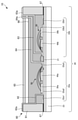
- FIG. 2 is a cross-sectional view of the semiconductor device of the second embodiment
- FIG. 3 is a plan view of the semiconductor device of the second embodiment
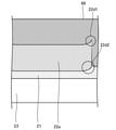
- FIG. 4 is a diagram for explaining the circuit pattern of the second embodiment
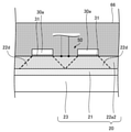
- 5 and 6 are cross-sectional views of a main part of the semiconductor device according to the second embodiment. Note that FIG. 2 shows a cross-sectional view taken along the alternate long and short dash line XX of FIG. Further, in FIG. 3, the description of the case 60 of the semiconductor device 10 and the sealing member 66 is omitted.
- FIG. 3 shows a cross-sectional view taken along the alternate long and short dash line XX of FIG.
- FIG. 4 is an enlarged cross-sectional view of an arbitrary circuit pattern.
- FIG. 5 shows a cross-sectional view taken along the alternate long and short dash line YY of FIG.
- FIG. 6 illustrates a case where the wire 50 is connected instead of the slit 22c1 in the case of FIG.
- the semiconductor device 10 includes an insulating circuit board 20, semiconductor chips 30a, 40a, 30b, 40b, and a case 60 for accommodating the insulating circuit board 20 and the semiconductor chips 30a, 40a, 30b, 40b.
- the insulating circuit board 20 includes a resin layer 21, circuit patterns 22a and 22b, and a base plate 23.
- the circuit patterns 22a and 22b are generic names for the circuit patterns 22a1 to 22a3 and 22b1 to 22b3. In the following, when the circuit patterns 22a1 to 22a3 and 22b1 to 22b3 are not distinguished, they are referred to as circuit patterns 22a and 22b.
- the resin layer 21 is made of a resin having low thermal resistance and high insulating properties.
- a resin is, for example, a thermosetting resin.
- the thermosetting resin may contain a thermally conductive filler.
- a thermosetting resin for example, at least one of epoxy resin, cyanate resin, benzoxazine resin, unsaturated polyester resin, phenol resin, melamine resin, silicone resin, maleimide resin, acrylic resin, and polyamide resin is used. Used.
- the thermally conductive filler is composed of at least one of an oxide or a nitride.
- the oxide is, for example, silicon oxide or aluminum oxide.
- the nitride is, for example, silicon nitride, aluminum nitride, or boron nitride. Further, hexagonal boron nitride may be used as the thermally conductive filler.
- the thickness of such a resin layer 21 depends on the rated voltage of the semiconductor device 10. That is, it is desired that the thickness of the resin layer 21 is increased as the rated voltage of the semiconductor device 10 is higher. On the other hand, it is also desired to make the resin layer 21 as thin as possible to reduce the thermal resistance.
- the thickness of such a resin layer 21 is, for example, 0.05 mm or more and 0.50 mm or less.
- the circuit patterns 22a and 22b are made of a material having excellent conductivity. Such a material is made of, for example, copper, aluminum, or an alloy containing at least one of these.
- the thickness of the circuit patterns 22a and 22b is preferably 0.1 mm or more and 5.0 mm or less, and more preferably 0.2 mm or more and 2.0 mm or less. The details of the thickness of each of the circuit patterns 22a and 22b will be described later.
- the circuit patterns 22a and 22b are obtained by punching one conductive plate so as to have a desired pattern shape.
- burrs are generated on the outer peripheral end portion of the main surface according to the punching direction, and sagging is generated on the outer peripheral end portion of the main surface on the opposite side of the main surface.
- the circuit pattern 22a is arranged on the resin layer 21 so that the sagging 22d2 is located on the back surface facing the resin layer 21 and the burr 22d1 is located on the front surface.
- the circuit pattern 22a is arranged so that the burr 22d1 is located on the back surface of the resin layer 21.
- the burr 22d1 may break through the resin layer 21 depending on the thickness of the resin layer 21, the burr 22d1 may break through the resin layer 21.
- the resin layer 21 cannot maintain the insulating property between the circuit pattern 22a and the base plate 23.
- the circuit pattern 22a is arranged with respect to the resin layer 21 so that the sagging 22d2 is located on the back surface of the circuit pattern 22a. In this case, the sagging 22d2 easily adheres to the resin layer 21. Therefore, the circuit pattern 22a is securely fixed to the resin layer 21, and the circuit pattern 22a is prevented from peeling from the resin layer 21.
- the circuit pattern 22b in which the burrs 22d1 and the sagging 22d2 are generated is also arranged in the resin layer 21 in the same manner as described above.
- the semiconductor chips 30a and 40a and the semiconductor chips 30b and 40b are joined to the circuit pattern 22a2 and the circuit pattern 22b2 via solder.
- wiring members such as wires, lead frames and connection terminals and electronic components are appropriately placed on the circuit pattern 22a and the circuit pattern 22b.
- the squares described in the circuit patterns 22a2, 22a3, 22b1, 22b2 represent the joints of the lead frames 62 to 64. It is also possible to perform plating on such circuit patterns 22a and 22b with a material having excellent corrosion resistance. Such materials are, for example, nickel, or alloys containing at least one of these.
- slits 22c1 are formed between the semiconductor chips 30a and between the semiconductor chips 40a, respectively.
- FIG. 5 shows a case where the slit 22c1 is formed between the semiconductor chips 30a.
- slits 22c2 are formed between the semiconductor chips 30b and the semiconductor chips 40b, respectively.
- the slit 22c1 can reduce thermal interference between the semiconductor chips 30a and the semiconductor chips 40a.
- the slit 22c2 can also reduce thermal interference between the semiconductor chips 30b and the semiconductor chips 40b.
- circuit patterns 22a and 22b shown in FIGS. 2 and 3 are examples, and the number, arrangement position, and shape can be appropriately selected by design, not limited to this case.
- the base plate 23 is made of a material having excellent thermal conductivity.
- the material is, for example, aluminum, iron, silver, copper, or an alloy containing at least one of these. Further, as such a material, a metal composite material may be used. Examples of the metal composite material include aluminum-silicon nitride (Al-SiC) and magnesium-silicon nitride (Mg-SiC). Further, in order to improve the corrosion resistance, the surface of the base plate 23 may be plated.
- the plating material at this time includes, for example, nickel, nickel-phosphorus alloy, nickel-boron alloy and the like.
- the thickness of the plating film is preferably 1 ⁇ m or more, more preferably 5 ⁇ m or more.
- a cooling unit (not shown) can be attached to the back surface of the base plate 23 via solder, silver brazing, or the like. This makes it possible to improve the heat dissipation of the semiconductor device 10.
- the cooling unit in this case is made of, for example, a metal having excellent thermal conductivity.
- the metal is aluminum, iron, silver, copper, or an alloy containing at least one of these.
- the cooling unit is a heat sink provided with one or more fins, a water-cooled cooling device, or the like.
- the base plate 23 may be integrated with such a cooling unit. In that case, it is composed of aluminum, iron, silver, copper, or an alloy containing at least one of these, which has excellent thermal conductivity.
- the surface of the base plate 23 integrated with the cooling unit may be plated.
- the plating material at this time includes, for example, nickel, nickel-phosphorus alloy, nickel-boron alloy and the like.
- the thickness of the base plate 23 is preferably 2 mm or more and 10 mm or less.
- the difference in linear expansion coefficient between the circuit patterns 22a and 22b and the base plate 23 and the resin layer 21 can be reduced. Therefore, even if the semiconductor chips 30a, 40a, 30b, and 40b generate heat, the occurrence of warpage of the insulating circuit board 20 can be reduced.
- the thermal resistance in the circuit pattern 22a2 and the circuit pattern 22b2 (when the thickness is constant) in which the semiconductor chips 30a and 40a and the semiconductor chips 30b and 40b are arranged is the same as that of the semiconductor chips 30a and 40a and the semiconductor chips 30b and 40b. It is related to the chip area. That is, the thermal resistance in the circuit pattern 22a2 and the circuit pattern 22b2 decreases as the respective chip areas increase. Further, the thermal resistance in the circuit pattern 22a2 and the circuit pattern 22b2 (the chip area is constant) is related to the thickness of the circuit pattern 22a2 and the circuit pattern 22b2.
- the thermal resistance in the circuit pattern 22a2 and the circuit pattern 22b2 decreases. Therefore, when the thicknesses of the circuit pattern 22a2 and the circuit pattern 22b2 are 0.1 mm, 0.3 mm, 0.4 mm, 0.5 mm, 0.8 mm, and 1.0 mm, respectively, the chip area is changed. The thermal resistance in the circuit pattern 22a2 and the circuit pattern 22b2 was measured. According to this, in any of the above cases, the thermal resistance of the circuit pattern 22a2 and the circuit pattern 22b2 decreased as the chip area increased, regardless of the thickness of the circuit pattern 22a2 and the circuit pattern 22b2.
- the thickness of the circuit pattern 22a2 and the circuit pattern 22b2 is preferably 0.5 mm or more.
- the circuit patterns 22a3 and 22b3 are required to have a certain thickness because the output current is input from the semiconductor chips 30a and 30b. Therefore, in consideration of cost reduction in manufacturing and the like, the thickness of the circuit patterns 22a3 and 22b3 is also preferably 0.5 mm or more, similarly to the circuit patterns 22a2 and 22b2.
- the circuit patterns 22a1,22b1 the control signals for the semiconductor chips 30a and 30b are conducted. Therefore, the circuit patterns 22a1,22b1 are not required to have high heat dissipation. Therefore, the circuit patterns 22a1,22b1 do not need to be as thick as the other circuit patterns 22a2, 22a3, 22b2, 22b3.
- Such an insulated circuit board 20 is formed, for example, as follows. First, the circuit patterns 22a and 22b are obtained in advance by punching from the conductive plate. The circuit patterns 22a and 22b thus obtained, the resin layer 21 and the base plate 23 are laminated, and each is crimped by heating and pressurizing in the stacking direction. Such crimping is performed in an activated gas atmosphere or in vacuum. As a result, the insulated circuit board 20 is obtained. Alternatively, the following method may be used. First, the base plate 23, the resin layer 21, and the conductive plate are laminated in order, and each is crimped by heating and pressurizing in the stacking direction in the same manner as described above.
- the conductive plate is aligned with a predetermined pattern, masked with a photosensitive resist mask, a pattern is formed by etching, and the photosensitive resist mask is removed to form circuit patterns 22a and 22b.
- the insulated circuit board 20 can be obtained by disassembling what is formed in this way.
- the semiconductor chips 30a, 40a, 30b, 40b are power devices composed mainly of silicon or a wide bandgap semiconductor.
- the wide bandgap semiconductor is, for example, silicon nitride or gallium nitride. Further, the chip area (length of one side) of the semiconductor chips 30a, 40a, 30b, 40b is 5.5 mm or less.
- the semiconductor chips 30a and 30b include a switching element.
- the switching element is a power MOSFET or an IGBT.
- a drain electrode positive electrode, a collector electrode in an IGBT
- a gate electrode control electrode
- a source electrode negative electrode
- An electrode and an emitter electrode in the case of IGBT are provided respectively.
- the semiconductor chips 40a and 40b include a diode element.
- the diode element is an FWD (Free Wheeling Diode) such as an SBD (Schottky Barrier Diode) or a PiN (P-intrinsic-N) diode.
- Such semiconductor chips 40a and 40b are provided with a cathode electrode as a main electrode on the back surface and an anode electrode as a main electrode on the front surface.
- the back surfaces of the semiconductor chips 30a and 40a and the semiconductor chips 30b and 40b are bonded to the circuit pattern 22a2 and the circuit pattern 22b2 by solder 31 (see FIG. 5 and the like).
- the solder 31 is composed of lead-free solder containing a predetermined alloy as a main component.
- the predetermined alloy is, for example, at least one of an alloy composed of tin-silver-copper, an alloy composed of tin-zinc-bismuth, an alloy composed of tin-copper, and an alloy composed of tin-silver-indium-bismuth.
- the solder 31 may contain additives. Additives are, for example, nickel, germanium, cobalt or silicon.
- the bonding may be performed by sintering using a sintering material.
- the sintered material in this case is, for example, a powder containing copper and aluminum as main components.
- the thicknesses of the semiconductor chips 30a, 40a, 30b, and 40b are, for example, 80 ⁇ m or more and 500 ⁇ m or less, and the average is about 200 ⁇ m.
- Electronic components may be arranged in the circuit patterns 22a and 22b, if necessary. Electronic components are, for example, capacitors, resistors, thermistors, current sensors, and control ICs (Integrated Circuits). Further, instead of the semiconductor chips 30a and 40a and the semiconductor chips 30b and 40b, a semiconductor chip including an RC (Reverse Conducting) -IGBT switching element in which the IGBT and the FWD are configured in one chip may be arranged.
- RC Reverse Conducting
- the semiconductor chips 30a and 40a are separated inward from the outer peripheral end of the circuit pattern 22a2 by a distance corresponding to the thickness of the circuit pattern 22a2 or more.
- the semiconductor chips 30b and 40b are also separated inward from the outer peripheral end of the circuit pattern 22b2 by a distance corresponding to the thickness of the circuit pattern 22b2 or more.
- the heat diffusion portions for the circuit patterns 22a2 and the circuit patterns 22b2 of the heat from the semiconductor chips 30a and 40a and the semiconductor chips 30b and 40b are not interfered with each other from the outside.
- the heat diffusion portions 22d are also provided in the circuit pattern 22a2 at intervals so as not to interfere with each other in the circuit pattern 22a2 between the semiconductor chips 30a.
- the slit 22c1 formed between the semiconductor chips 30a is formed in the circuit pattern 22a2 at a depth that does not interfere with the two heat diffusion portions 22d.
- the slit 22c1 does not hinder the suppression of the deterioration of the heat dissipation property of the circuit pattern 22a2 with respect to the semiconductor chip 30a.
- the wire 50 may be connected between the semiconductor chips 30a as shown in FIG. Even in this case, the wire 50 does not hinder the suppression of the deterioration of the heat dissipation property of the circuit pattern 22a2 with respect to the semiconductor chip 30a. The same applies to the case where the wires 50 are connected between the semiconductor chips 40a, the semiconductor chips 30b, and the semiconductor chips 40b, respectively. The details of the wire 50 will be described below.
- the wire 50 is formed between the main electrodes of the semiconductor chips 30a and 40a and the semiconductor chips 30b and 40b and the circuit pattern 22a and the circuit pattern 22b, between the main electrodes of the semiconductor chips 30a and 40a, and the main electrodes of the semiconductor chips 30b and 40b. Connect the spaces electrically and mechanically as appropriate. Further, the wires 51a and 51b are electrically and mechanically connected between the circuit patterns 22a1, 22b1 and the control electrodes of the semiconductor chips 30a and 30b.
- Such wires 50, 51a, 51b are made of a material having excellent conductivity. The material is composed of, for example, gold, silver, copper, aluminum, or an alloy containing at least one of these.
- the diameter of the wire 50 is, for example, 390 ⁇ m or more and 410 ⁇ m or less.
- the diameters of the wires 51a and 51b are, for example, 120 ⁇ m or more and 130 ⁇ m or less.
- the case 60 has a frame body portion 61 and a lid portion 65 provided at the upper portion of the opening of the frame body portion 61.
- the frame body portion 61 has an opening formed from the front surface to the back surface in the central portion, and forms a frame shape in a plan view.
- the frame body portion 61 includes lead frames 62 to 64.
- the frame body portion 61 is integrally formed with the lead frames 62 to 64 by insert molding. In insert molding, a thermoplastic resin that can be bonded to the lead frames 62 to 64 is used. Examples of such resins include polyphenylene sulfide, polybutylene terephthalate resin, polybutylene succinate resin, polyamide resin, and acrylonitrile butadiene styrene resin.
- the lid portion 65 is also made of the same material as the frame body portion 61.
- the lead frames 62 to 64 have a crank shape in the side view shown in FIG. 2, for example.
- the terminals 62a to 64a at one end of the lead frames 62 to 64 project from the upper surface of the lid portion 65 of the case 60 and are arranged on the frame body portion 61.
- the other ends of the lead frames 62 to 64 are electrically and mechanically bonded to the circuit patterns 22a2, 22a3, and 22b2 by soldering (not shown) in the frame body portion 61.
- Such lead frames 62 to 64 are made of a material having excellent conductivity. Such a material is made of, for example, copper, aluminum, or an alloy containing at least one of these.
- the thickness of the lead frames 62 to 64 is preferably 1.00 mm or more and 2.00 mm or less, and more preferably 1.20 mm or more and 1.50 mm or less.
- the lead frames 62 to 64 can also be plated with a material having excellent corrosion resistance. Such a material is, for example, nickel, an alloy containing nickel, or the like.
- the back surface of the frame body portion 61 of the case 60 is fixed to the outer peripheral end portion of the insulating circuit board 20 (resin layer 21) by the adhesive member 67.
- the adhesive member 67 for example, a thermosetting resin-based adhesive member or an organic-based adhesive member is used.
- the thermosetting resin-based adhesive member contains, for example, an epoxy resin or a phenol resin as a main component.
- the organic adhesive member is, for example, an elastomer adhesive containing silicone rubber or chloroprene rubber as a main component. In this way, the semiconductor chips 30a, 40a, 30b, 40b and the like are housed in the opening of the frame body portion 61, and the inside of the opening is sealed by the sealing member 66.
- the sealing member 66 may be capable of sealing the insulating circuit board 20, the semiconductor chips 30a, 40a, 30b, 40b, and the wires 50, 51a, 51b at the opening of the frame body portion 61. It is not necessary to fill the entire opening of the frame portion 61 with the sealing member 66.
- the sealing member 66 contains a thermosetting resin and a filler contained in the thermosetting resin.
- the thermosetting resin is, for example, an epoxy resin, a phenol resin, a maleimide resin, or a polyester resin.
- the sealing member 66 there is an epoxy resin, and the epoxy resin contains a filler.
- the filler is, for example, silicon oxide, aluminum oxide, boron nitride or aluminum nitride.
- the sealing member 66 may use a thermoplastic resin.
- the thermoplastic resin is, for example, a polyphenylene sulfide resin, a polybutylene terephthalate resin, a polybutylene succinate resin, a polyamide resin, or an acrylonitrile butadiene styrene resin.
- the sealed member 66 in a molten state is injected into the case 60.
- the sealing member 66, the case 60, and the semiconductor chips 30a, 40a, 30b, and 40b are heated so as to maintain a predetermined temperature. ..
- the sealing member 66 spreads to every corner of the case 60 without generating voids. Further, such a sealing member 66 is defoamed to remove voids in a vacuum before being injected.
- the sealed member 66 in a molten state is stirred in a vacuum to completely defoam, so that the generation of further voids can be suppressed.
- ultrasonic vibration may be applied to the case 60, the insulating circuit board 20, and the like when the sealing member 66 in the molten state is injected. This makes it possible to more reliably suppress the generation of voids in the sealing member 66.
- the difference in the coefficient of thermal expansion between the base plate 23 included in the insulating circuit board 20, the resin layer 21, and the circuit patterns 22a and 22b is small, and the warp of the insulating circuit board 20 due to heat is reduced. Can be done.
- the side ends of the circuit pattern 22a2 and the circuit pattern 22b2 are at least a predetermined distance from the outer peripheral end of the circuit pattern 22a2 and the circuit pattern 22b2 on the front surface of the circuit pattern 22a2 and the circuit pattern 22b2. They are joined apart from each other inward.
- the heat diffusion portions of the circuit patterns 22a2 and the circuit patterns 22b2 by the semiconductor chips 30a and 40a and the semiconductor chips 30b and 40b are not interfered with each other, and the circuit patterns 22a2 and the circuit patterns 22a2 for the semiconductor chips 30a and 40a and the semiconductor chips 30b and 40b It is possible to suppress a decrease in heat dissipation of the circuit pattern 22b2. Therefore, it is possible to suppress a decrease in long-term reliability as well as a decrease in heat dissipation of the semiconductor device 10.
- FIG. 7 is a cross-sectional view of a main part of the semiconductor device according to the third embodiment.
- FIG. 7 corresponds to a cross-sectional view taken along the alternate long and short dash line XX of the semiconductor device 10 shown in FIG. 3, and shows the periphery of the semiconductor chip 40a in this cross-sectional view.
- the cross sections of the circuit patterns 22a2 and 22a3 are shown in a rectangular shape. As shown in FIG. 4, the circuit patterns 22a2 and 22a3 may have burrs on the front surface side and sagging on the back surface side.
- the insulating circuit board 20 In this case, in the insulating circuit board 20, about half of the lower part of the circuit patterns 22a2 and 22a3 is embedded in the resin layer 21.
- the sealing member 66 enters between the circuit patterns 22a2 and 22a3, and the circuit patterns 22a2 and 22a3 are pressed toward the base plate 23 side. Therefore, it is possible to prevent the circuit patterns 22a2 and 22a3 from peeling from the resin layer 21. Even if the side portions of the circuit patterns 22a2 and 22a3 are peeled off from the resin layer 21, the deterioration of the heat dissipation of the insulating circuit board 20 is small.
- FIGS. 8 and 9 are cross-sectional views of a main part of the semiconductor device according to the fourth embodiment. 8 and 9 correspond to the cross-sectional view of the one-dot chain line XX of the semiconductor device 10 shown in FIG. 3, and show the periphery of the semiconductor chip 40a in this cross-sectional view. Further, in FIGS. 8 and 9, the cross sections of the circuit patterns 22a2 and 22a3 are shown in a rectangular shape. As shown in FIG. 4, the circuit patterns 22a2 and 22a3 may have burrs on the front surface side and sagging on the back surface side.
- the circuit patterns 22a2 and 22a3 are embedded in the resin layer 21 so that the front surface of the circuit pattern 22a2 and 22a3 forms the same plane as the front surface of the resin layer 21. ..
- the insulating circuit board 20 is obtained by crimping the circuit patterns 22a and 22b to the resin layer 21. At the time of this crimping, the circuit patterns 22a and 22b are pressed against the resin layer 21 with a larger pressure. As a result, the circuit patterns 22a and 22b are embedded in the resin layer 21.
- the resin layer 21 pressed by the circuit patterns 22a and 22b protrudes from the gaps of the circuit patterns 22a2 and 22a3, for example, as shown in FIG. Then, the resin layer 21 between the circuit patterns 22a2 and 22a3 and the circuit patterns 22a2 and 22a3 is sealed by the sealing member 66 and pressed against the base plate 23 side. Therefore, as in the third embodiment, peeling of the circuit patterns 22a2 and 22a3 from the resin layer 21 can be prevented, and deterioration of the heat dissipation property of the insulating circuit board 20 can be prevented. Further, the resin layer 21 projects from between the circuit patterns 22a2 and 22a3.
- the length (creeping distance) of the interface between the sealing member 66 and the resin layer 21 becomes long, and the insulating property between the circuit patterns 22a2 and 22a3 and the base plate 23 is improved.
- This is not limited to the circuit patterns 22a2 and 22a3, but is the same for other circuit patterns 22a and 22b. Therefore, it is possible to suppress a decrease in long-term reliability as well as a decrease in heat dissipation of the semiconductor device 10.
- the circuit patterns 22a2 and 22a3 may wrap around to the front surface side. Also in this case, similarly to FIG. 8, the length (creeping distance) of the interface between the sealing member 66 and the resin layer 21 becomes longer, and the insulating property between the circuit patterns 22a2 and 22a3 and the base plate 23 is improved. Further, the circuit patterns 22a2 and 22a3 are pressed toward the base plate 23 side by the resin layer 21 that wraps around the front surface side of the circuit patterns 22a2 and 22a3. Therefore, peeling of the circuit patterns 22a2 and 22a3 can be further prevented. This is not limited to the circuit patterns 22a2 and 22a3, but is the same for other circuit patterns 22a and 22b.
- FIG. 10 is a cross-sectional view of a main part of the semiconductor device according to the fifth embodiment. Note that FIG. 10 corresponds to the cross-sectional view of the one-dot chain line XX of the semiconductor device 10 shown in FIG. 3, and shows the periphery of the semiconductor chip 40a in this cross-sectional view.
- the corners are chamfered along the outer peripheral end of the circuit patterns 22a2 and 22a3 included in the insulating circuit board 20 on the front surface side.
- the chamfering angle is, for example, an angle that does not enter the heat diffusion portion with respect to the circuit pattern 22a2 of the semiconductor chip 40a.
- Such circuit patterns 22a2 and 22a3 are sealed by the sealing member 66.
- the corners of the circuit patterns 22a2 and 22a3 are not chamfered as in the case of FIG. 7, the corners of the circuit patterns 22a2 and 22a3 are the starting points of cracks with respect to the sealing member 66. There is.
Landscapes
- Structures Or Materials For Encapsulating Or Coating Semiconductor Devices Or Solid State Devices (AREA)
- Cooling Or The Like Of Semiconductors Or Solid State Devices (AREA)
- Physics & Mathematics (AREA)
- Geometry (AREA)
Priority Applications (6)
| Application Number | Priority Date | Filing Date | Title |
|---|---|---|---|
| JP2022545493A JP7428261B2 (ja) | 2020-08-28 | 2021-07-01 | 半導体装置 |
| DE112021000290.2T DE112021000290T5 (de) | 2020-08-28 | 2021-07-01 | Halbleitervorrichtung |
| CN202180010705.XA CN115004359A (zh) | 2020-08-28 | 2021-07-01 | 半导体装置 |
| US17/876,228 US12469792B2 (en) | 2020-08-28 | 2022-07-28 | Semiconductor device |
| JP2023194122A JP7729368B2 (ja) | 2020-08-28 | 2023-11-15 | 半導体装置 |
| US19/376,025 US20260060115A1 (en) | 2020-08-28 | 2025-10-31 | Semiconductor device |
Applications Claiming Priority (2)
| Application Number | Priority Date | Filing Date | Title |
|---|---|---|---|
| JP2020-144178 | 2020-08-28 | ||
| JP2020144178 | 2020-08-28 |
Related Child Applications (1)
| Application Number | Title | Priority Date | Filing Date |
|---|---|---|---|
| US17/876,228 Continuation US12469792B2 (en) | 2020-08-28 | 2022-07-28 | Semiconductor device |
Publications (1)
| Publication Number | Publication Date |
|---|---|
| WO2022044541A1 true WO2022044541A1 (ja) | 2022-03-03 |
Family
ID=80353138
Family Applications (1)
| Application Number | Title | Priority Date | Filing Date |
|---|---|---|---|
| PCT/JP2021/024996 Ceased WO2022044541A1 (ja) | 2020-08-28 | 2021-07-01 | 半導体装置 |
Country Status (5)
| Country | Link |
|---|---|
| US (2) | US12469792B2 (https=) |
| JP (2) | JP7428261B2 (https=) |
| CN (1) | CN115004359A (https=) |
| DE (1) | DE112021000290T5 (https=) |
| WO (1) | WO2022044541A1 (https=) |
Cited By (3)
| Publication number | Priority date | Publication date | Assignee | Title |
|---|---|---|---|---|
| JP2024003177A (ja) * | 2020-08-28 | 2024-01-11 | 富士電機株式会社 | 半導体装置 |
| DE102024105408A1 (de) | 2023-05-11 | 2024-11-14 | Fuji Electric Co., Ltd. | Halbleitervorrichtung |
| WO2025192191A1 (ja) * | 2024-03-11 | 2025-09-18 | ローム株式会社 | 半導体装置、電力変換ユニットおよび車両 |
Citations (7)
| Publication number | Priority date | Publication date | Assignee | Title |
|---|---|---|---|---|
| JP2006319146A (ja) * | 2005-05-13 | 2006-11-24 | Fuji Electric Holdings Co Ltd | 配線基板 |
| JP2010103311A (ja) * | 2008-10-23 | 2010-05-06 | Toyota Central R&D Labs Inc | 積層基板 |
| JP2012531728A (ja) * | 2009-07-02 | 2012-12-10 | キュラミーク エレクトロニクス ゲーエムベーハー | 電子装置 |
| JP2013207226A (ja) * | 2012-03-29 | 2013-10-07 | Sumitomo Electric Device Innovations Inc | 半導体チップ実装基板 |
| JP2014022579A (ja) * | 2012-07-19 | 2014-02-03 | Rohm Co Ltd | パワーモジュール半導体装置 |
| JP2017199830A (ja) * | 2016-04-28 | 2017-11-02 | 三菱電機株式会社 | パワーモジュール |
| JP2019071399A (ja) * | 2016-11-21 | 2019-05-09 | ローム株式会社 | パワーモジュールおよびその製造方法、グラファイトプレート、および電源装置 |
Family Cites Families (23)
| Publication number | Priority date | Publication date | Assignee | Title |
|---|---|---|---|---|
| JP3199193B2 (ja) | 1992-11-20 | 2001-08-13 | 電気化学工業株式会社 | 半導体搭載用回路基板およびその製造方法 |
| JPH06350212A (ja) | 1993-06-11 | 1994-12-22 | Denki Kagaku Kogyo Kk | 金属ベース回路基板とその製造方法 |
| JP3110298B2 (ja) * | 1995-10-31 | 2000-11-20 | 松下電子工業株式会社 | 半導体装置 |
| JPH11186679A (ja) | 1997-12-18 | 1999-07-09 | Fuji Electric Co Ltd | 絶縁基板およびその製造方法 |
| JP2001044342A (ja) | 1999-07-29 | 2001-02-16 | Sanyo Electric Co Ltd | 混成集積回路装置 |
| JP2002217508A (ja) | 2001-01-19 | 2002-08-02 | Fuji Electric Co Ltd | 金属ベース基板およびその製造方法 |
| JP2002246515A (ja) * | 2001-02-20 | 2002-08-30 | Mitsubishi Electric Corp | 半導体装置 |
| JP4992302B2 (ja) | 2005-07-05 | 2012-08-08 | 富士電機株式会社 | パワー半導体モジュール |
| JP4904916B2 (ja) * | 2006-05-18 | 2012-03-28 | 三菱マテリアル株式会社 | パワーモジュール用基板およびパワーモジュール用基板の製造方法並びにパワーモジュール |
| JP5552803B2 (ja) * | 2009-12-07 | 2014-07-16 | 三菱マテリアル株式会社 | パワーモジュール用基板の製造方法 |
| JP5010669B2 (ja) * | 2009-12-07 | 2012-08-29 | パナソニック株式会社 | 配線基板及びその製造方法 |
| JP2012191057A (ja) | 2011-03-11 | 2012-10-04 | Mitsubishi Electric Corp | 電力用半導体装置 |
| JP2013080860A (ja) | 2011-10-05 | 2013-05-02 | Rohm Co Ltd | Led光源装置 |
| JP5848976B2 (ja) | 2012-01-25 | 2016-01-27 | 新光電気工業株式会社 | 配線基板、発光装置及び配線基板の製造方法 |
| DE112012006656B4 (de) * | 2012-07-05 | 2021-08-05 | Mitsubishi Electric Corporation | Halbleitervorrichtung |
| US9627302B2 (en) * | 2014-01-10 | 2017-04-18 | Mitsubishi Electric Corporation | Power semiconductor device |
| JP2015208200A (ja) * | 2014-04-23 | 2015-11-19 | 株式会社デンソー | 電源装置 |
| JP6320331B2 (ja) | 2015-03-16 | 2018-05-09 | 三菱電機株式会社 | 電力用半導体装置 |
| JP6721329B2 (ja) | 2015-12-21 | 2020-07-15 | 三菱電機株式会社 | パワー半導体装置およびその製造方法 |
| JP6790372B2 (ja) | 2016-02-05 | 2020-11-25 | 富士電機株式会社 | 半導体装置 |
| US11367669B2 (en) | 2016-11-21 | 2022-06-21 | Rohm Co., Ltd. | Power module and fabrication method of the same, graphite plate, and power supply equipment |
| JP2019169540A (ja) | 2018-03-22 | 2019-10-03 | 三菱マテリアル株式会社 | 絶縁回路基板、および、絶縁回路基板の製造方法 |
| CN115004359A (zh) | 2020-08-28 | 2022-09-02 | 富士电机株式会社 | 半导体装置 |
-
2021
- 2021-07-01 CN CN202180010705.XA patent/CN115004359A/zh active Pending
- 2021-07-01 JP JP2022545493A patent/JP7428261B2/ja active Active
- 2021-07-01 WO PCT/JP2021/024996 patent/WO2022044541A1/ja not_active Ceased
- 2021-07-01 DE DE112021000290.2T patent/DE112021000290T5/de active Pending
-
2022
- 2022-07-28 US US17/876,228 patent/US12469792B2/en active Active
-
2023
- 2023-11-15 JP JP2023194122A patent/JP7729368B2/ja active Active
-
2025
- 2025-10-31 US US19/376,025 patent/US20260060115A1/en active Pending
Patent Citations (7)
| Publication number | Priority date | Publication date | Assignee | Title |
|---|---|---|---|---|
| JP2006319146A (ja) * | 2005-05-13 | 2006-11-24 | Fuji Electric Holdings Co Ltd | 配線基板 |
| JP2010103311A (ja) * | 2008-10-23 | 2010-05-06 | Toyota Central R&D Labs Inc | 積層基板 |
| JP2012531728A (ja) * | 2009-07-02 | 2012-12-10 | キュラミーク エレクトロニクス ゲーエムベーハー | 電子装置 |
| JP2013207226A (ja) * | 2012-03-29 | 2013-10-07 | Sumitomo Electric Device Innovations Inc | 半導体チップ実装基板 |
| JP2014022579A (ja) * | 2012-07-19 | 2014-02-03 | Rohm Co Ltd | パワーモジュール半導体装置 |
| JP2017199830A (ja) * | 2016-04-28 | 2017-11-02 | 三菱電機株式会社 | パワーモジュール |
| JP2019071399A (ja) * | 2016-11-21 | 2019-05-09 | ローム株式会社 | パワーモジュールおよびその製造方法、グラファイトプレート、および電源装置 |
Cited By (4)
| Publication number | Priority date | Publication date | Assignee | Title |
|---|---|---|---|---|
| JP2024003177A (ja) * | 2020-08-28 | 2024-01-11 | 富士電機株式会社 | 半導体装置 |
| JP7729368B2 (ja) | 2020-08-28 | 2025-08-26 | 富士電機株式会社 | 半導体装置 |
| DE102024105408A1 (de) | 2023-05-11 | 2024-11-14 | Fuji Electric Co., Ltd. | Halbleitervorrichtung |
| WO2025192191A1 (ja) * | 2024-03-11 | 2025-09-18 | ローム株式会社 | 半導体装置、電力変換ユニットおよび車両 |
Also Published As
| Publication number | Publication date |
|---|---|
| CN115004359A (zh) | 2022-09-02 |
| JP7729368B2 (ja) | 2025-08-26 |
| JP7428261B2 (ja) | 2024-02-06 |
| JP2024003177A (ja) | 2024-01-11 |
| US12469792B2 (en) | 2025-11-11 |
| JPWO2022044541A1 (https=) | 2022-03-03 |
| DE112021000290T5 (de) | 2022-11-03 |
| US20220367372A1 (en) | 2022-11-17 |
| US20260060115A1 (en) | 2026-02-26 |
Similar Documents
| Publication | Publication Date | Title |
|---|---|---|
| JP7729368B2 (ja) | 半導体装置 | |
| CN111081643B (zh) | 半导体装置及半导体装置的制造方法 | |
| JP6370257B2 (ja) | 半導体装置 | |
| WO2018135239A1 (ja) | 半導体装置および電力変換装置 | |
| JP2019125708A (ja) | 半導体装置 | |
| JP2022053848A (ja) | 半導体装置 | |
| US20210366796A1 (en) | Semiconductor device | |
| US20210257269A1 (en) | Semiconductor device | |
| JP7237647B2 (ja) | 回路基板および電子装置 | |
| JPWO2022044541A5 (https=) | ||
| US20230253275A1 (en) | Semiconductor device and semiconductor device manufacturing method | |
| CN108735722B (zh) | 半导体装置及半导体装置的制造方法 | |
| CN113163586B (zh) | 半导体装置 | |
| JP2023074141A (ja) | 半導体装置の製造方法及び治具セット | |
| US20250380362A1 (en) | Circuit assembly with two circuit carriers and a semiconductor component | |
| JP2021158304A (ja) | 半導体装置及び半導体装置の製造方法 | |
| WO2024185127A1 (ja) | 半導体装置及びその製造方法 | |
| JP6992913B2 (ja) | リードフレーム配線構造及び半導体モジュール | |
| WO2021241304A1 (ja) | 半導体モジュールの実装構造 | |
| JP2022050058A (ja) | 半導体装置及び半導体装置の製造方法 | |
| JP4861200B2 (ja) | パワーモジュール | |
| US20240071898A1 (en) | Semiconductor device and semiconductor device manufacturing method | |
| US12538822B2 (en) | Semiconductor device with improved control circuit pattern placement | |
| US20260123418A1 (en) | Semiconductor device | |
| WO2024190132A1 (ja) | 放熱ベース、半導体モジュール、及びエネルギー変換装置 |
Legal Events
| Date | Code | Title | Description |
|---|---|---|---|
| 121 | Ep: the epo has been informed by wipo that ep was designated in this application |
Ref document number: 21860971 Country of ref document: EP Kind code of ref document: A1 |
|
| ENP | Entry into the national phase |
Ref document number: 2022545493 Country of ref document: JP Kind code of ref document: A |
|
| 122 | Ep: pct application non-entry in european phase |
Ref document number: 21860971 Country of ref document: EP Kind code of ref document: A1 |