WO2022043826A1 - 半導体装置、表示装置、及び電子機器 - Google Patents
半導体装置、表示装置、及び電子機器 Download PDFInfo
- Publication number
- WO2022043826A1 WO2022043826A1 PCT/IB2021/057541 IB2021057541W WO2022043826A1 WO 2022043826 A1 WO2022043826 A1 WO 2022043826A1 IB 2021057541 W IB2021057541 W IB 2021057541W WO 2022043826 A1 WO2022043826 A1 WO 2022043826A1
- Authority
- WO
- WIPO (PCT)
- Prior art keywords
- transistor
- wiring
- potential
- circuit
- electrode
- Prior art date
- Legal status (The legal status is an assumption and is not a legal conclusion. Google has not performed a legal analysis and makes no representation as to the accuracy of the status listed.)
- Ceased
Links
Images




















Classifications
-
- H—ELECTRICITY
- H10—SEMICONDUCTOR DEVICES; ELECTRIC SOLID-STATE DEVICES NOT OTHERWISE PROVIDED FOR
- H10D—INORGANIC ELECTRIC SEMICONDUCTOR DEVICES
- H10D84/00—Integrated devices formed in or on semiconductor substrates that comprise only semiconducting layers, e.g. on Si wafers or on GaAs-on-Si wafers
- H10D84/80—Integrated devices formed in or on semiconductor substrates that comprise only semiconducting layers, e.g. on Si wafers or on GaAs-on-Si wafers characterised by the integration of at least one component covered by groups H10D12/00 or H10D30/00, e.g. integration of IGFETs
- H10D84/82—Integrated devices formed in or on semiconductor substrates that comprise only semiconducting layers, e.g. on Si wafers or on GaAs-on-Si wafers characterised by the integration of at least one component covered by groups H10D12/00 or H10D30/00, e.g. integration of IGFETs of only field-effect components
- H10D84/83—Integrated devices formed in or on semiconductor substrates that comprise only semiconducting layers, e.g. on Si wafers or on GaAs-on-Si wafers characterised by the integration of at least one component covered by groups H10D12/00 or H10D30/00, e.g. integration of IGFETs of only field-effect components of only insulated-gate FETs [IGFET]
- H10D84/85—Complementary IGFETs, e.g. CMOS
-
- H—ELECTRICITY
- H10—SEMICONDUCTOR DEVICES; ELECTRIC SOLID-STATE DEVICES NOT OTHERWISE PROVIDED FOR
- H10D—INORGANIC ELECTRIC SEMICONDUCTOR DEVICES
- H10D86/00—Integrated devices formed in or on insulating or conducting substrates, e.g. formed in silicon-on-insulator [SOI] substrates or on stainless steel or glass substrates
- H10D86/40—Integrated devices formed in or on insulating or conducting substrates, e.g. formed in silicon-on-insulator [SOI] substrates or on stainless steel or glass substrates characterised by multiple TFTs
- H10D86/421—Integrated devices formed in or on insulating or conducting substrates, e.g. formed in silicon-on-insulator [SOI] substrates or on stainless steel or glass substrates characterised by multiple TFTs having a particular composition, shape or crystalline structure of the active layer
- H10D86/423—Integrated devices formed in or on insulating or conducting substrates, e.g. formed in silicon-on-insulator [SOI] substrates or on stainless steel or glass substrates characterised by multiple TFTs having a particular composition, shape or crystalline structure of the active layer comprising semiconductor materials not belonging to the Group IV, e.g. InGaZnO
-
- G—PHYSICS
- G02—OPTICS
- G02F—OPTICAL DEVICES OR ARRANGEMENTS FOR THE CONTROL OF LIGHT BY MODIFICATION OF THE OPTICAL PROPERTIES OF THE MEDIA OF THE ELEMENTS INVOLVED THEREIN; NON-LINEAR OPTICS; FREQUENCY-CHANGING OF LIGHT; OPTICAL LOGIC ELEMENTS; OPTICAL ANALOGUE/DIGITAL CONVERTERS
- G02F1/00—Devices or arrangements for the control of the intensity, colour, phase, polarisation or direction of light arriving from an independent light source, e.g. switching, gating or modulating; Non-linear optics
- G02F1/01—Devices or arrangements for the control of the intensity, colour, phase, polarisation or direction of light arriving from an independent light source, e.g. switching, gating or modulating; Non-linear optics for the control of the intensity, phase, polarisation or colour
- G02F1/13—Devices or arrangements for the control of the intensity, colour, phase, polarisation or direction of light arriving from an independent light source, e.g. switching, gating or modulating; Non-linear optics for the control of the intensity, phase, polarisation or colour based on liquid crystals, e.g. single liquid crystal display cells
- G02F1/133—Constructional arrangements; Operation of liquid crystal cells; Circuit arrangements
- G02F1/136—Liquid crystal cells structurally associated with a semi-conducting layer or substrate, e.g. cells forming part of an integrated circuit
- G02F1/1362—Active matrix addressed cells
-
- G—PHYSICS
- G09—EDUCATION; CRYPTOGRAPHY; DISPLAY; ADVERTISING; SEALS
- G09G—ARRANGEMENTS OR CIRCUITS FOR CONTROL OF INDICATING DEVICES USING STATIC MEANS TO PRESENT VARIABLE INFORMATION
- G09G3/00—Control arrangements or circuits, of interest only in connection with visual indicators other than cathode-ray tubes
- G09G3/20—Control arrangements or circuits, of interest only in connection with visual indicators other than cathode-ray tubes for presentation of an assembly of a number of characters, e.g. a page, by composing the assembly by combination of individual elements arranged in a matrix no fixed position being assigned to or needed to be assigned to the individual characters or partial characters
-
- H—ELECTRICITY
- H10—SEMICONDUCTOR DEVICES; ELECTRIC SOLID-STATE DEVICES NOT OTHERWISE PROVIDED FOR
- H10D—INORGANIC ELECTRIC SEMICONDUCTOR DEVICES
- H10D30/00—Field-effect transistors [FET]
- H10D30/60—Insulated-gate field-effect transistors [IGFET]
- H10D30/67—Thin-film transistors [TFT]
- H10D30/674—Thin-film transistors [TFT] characterised by the active materials
- H10D30/6741—Group IV materials, e.g. germanium or silicon carbide
- H10D30/6743—Silicon
- H10D30/6745—Polycrystalline or microcrystalline silicon
-
- H—ELECTRICITY
- H10—SEMICONDUCTOR DEVICES; ELECTRIC SOLID-STATE DEVICES NOT OTHERWISE PROVIDED FOR
- H10D—INORGANIC ELECTRIC SEMICONDUCTOR DEVICES
- H10D30/00—Field-effect transistors [FET]
- H10D30/60—Insulated-gate field-effect transistors [IGFET]
- H10D30/67—Thin-film transistors [TFT]
- H10D30/674—Thin-film transistors [TFT] characterised by the active materials
- H10D30/6755—Oxide semiconductors, e.g. zinc oxide, copper aluminium oxide or cadmium stannate
-
- H—ELECTRICITY
- H10—SEMICONDUCTOR DEVICES; ELECTRIC SOLID-STATE DEVICES NOT OTHERWISE PROVIDED FOR
- H10D—INORGANIC ELECTRIC SEMICONDUCTOR DEVICES
- H10D86/00—Integrated devices formed in or on insulating or conducting substrates, e.g. formed in silicon-on-insulator [SOI] substrates or on stainless steel or glass substrates
- H10D86/40—Integrated devices formed in or on insulating or conducting substrates, e.g. formed in silicon-on-insulator [SOI] substrates or on stainless steel or glass substrates characterised by multiple TFTs
- H10D86/451—Integrated devices formed in or on insulating or conducting substrates, e.g. formed in silicon-on-insulator [SOI] substrates or on stainless steel or glass substrates characterised by multiple TFTs characterised by the compositions or shapes of the interlayer dielectrics
-
- H—ELECTRICITY
- H10—SEMICONDUCTOR DEVICES; ELECTRIC SOLID-STATE DEVICES NOT OTHERWISE PROVIDED FOR
- H10D—INORGANIC ELECTRIC SEMICONDUCTOR DEVICES
- H10D86/00—Integrated devices formed in or on insulating or conducting substrates, e.g. formed in silicon-on-insulator [SOI] substrates or on stainless steel or glass substrates
- H10D86/40—Integrated devices formed in or on insulating or conducting substrates, e.g. formed in silicon-on-insulator [SOI] substrates or on stainless steel or glass substrates characterised by multiple TFTs
- H10D86/60—Integrated devices formed in or on insulating or conducting substrates, e.g. formed in silicon-on-insulator [SOI] substrates or on stainless steel or glass substrates characterised by multiple TFTs wherein the TFTs are in active matrices
-
- H—ELECTRICITY
- H10—SEMICONDUCTOR DEVICES; ELECTRIC SOLID-STATE DEVICES NOT OTHERWISE PROVIDED FOR
- H10K—ORGANIC ELECTRIC SOLID-STATE DEVICES
- H10K59/00—Integrated devices, or assemblies of multiple devices, comprising at least one organic light-emitting element covered by group H10K50/00
- H10K59/10—OLED displays
- H10K59/12—Active-matrix OLED [AMOLED] displays
- H10K59/121—Active-matrix OLED [AMOLED] displays characterised by the geometry or disposition of pixel elements
- H10K59/1213—Active-matrix OLED [AMOLED] displays characterised by the geometry or disposition of pixel elements the pixel elements being TFTs
-
- G—PHYSICS
- G09—EDUCATION; CRYPTOGRAPHY; DISPLAY; ADVERTISING; SEALS
- G09G—ARRANGEMENTS OR CIRCUITS FOR CONTROL OF INDICATING DEVICES USING STATIC MEANS TO PRESENT VARIABLE INFORMATION
- G09G2300/00—Aspects of the constitution of display devices
- G09G2300/04—Structural and physical details of display devices
- G09G2300/0421—Structural details of the set of electrodes
- G09G2300/0426—Layout of electrodes and connections
-
- G—PHYSICS
- G09—EDUCATION; CRYPTOGRAPHY; DISPLAY; ADVERTISING; SEALS
- G09G—ARRANGEMENTS OR CIRCUITS FOR CONTROL OF INDICATING DEVICES USING STATIC MEANS TO PRESENT VARIABLE INFORMATION
- G09G2310/00—Command of the display device
- G09G2310/02—Addressing, scanning or driving the display screen or processing steps related thereto
- G09G2310/0264—Details of driving circuits
- G09G2310/0286—Details of a shift registers arranged for use in a driving circuit
-
- G—PHYSICS
- G09—EDUCATION; CRYPTOGRAPHY; DISPLAY; ADVERTISING; SEALS
- G09G—ARRANGEMENTS OR CIRCUITS FOR CONTROL OF INDICATING DEVICES USING STATIC MEANS TO PRESENT VARIABLE INFORMATION
- G09G2310/00—Command of the display device
- G09G2310/02—Addressing, scanning or driving the display screen or processing steps related thereto
- G09G2310/0264—Details of driving circuits
- G09G2310/0291—Details of output amplifiers or buffers arranged for use in a driving circuit
-
- G—PHYSICS
- G09—EDUCATION; CRYPTOGRAPHY; DISPLAY; ADVERTISING; SEALS
- G09G—ARRANGEMENTS OR CIRCUITS FOR CONTROL OF INDICATING DEVICES USING STATIC MEANS TO PRESENT VARIABLE INFORMATION
- G09G2310/00—Command of the display device
- G09G2310/08—Details of timing specific for flat panels, other than clock recovery
-
- G—PHYSICS
- G09—EDUCATION; CRYPTOGRAPHY; DISPLAY; ADVERTISING; SEALS
- G09G—ARRANGEMENTS OR CIRCUITS FOR CONTROL OF INDICATING DEVICES USING STATIC MEANS TO PRESENT VARIABLE INFORMATION
- G09G2330/00—Aspects of power supply; Aspects of display protection and defect management
- G09G2330/02—Details of power systems and of start or stop of display operation
- G09G2330/021—Power management, e.g. power saving
Definitions
- One aspect of the present invention relates to a semiconductor device.
- One aspect of the present invention relates to a display device.
- One aspect of the present invention relates to a drive circuit of a display device.
- one aspect of the present invention is not limited to the above technical fields.
- the technical fields of one aspect of the present invention disclosed in the present specification and the like include semiconductor devices, display devices, light emitting devices, power storage devices, storage devices, electronic devices, lighting devices, input devices, input / output devices, and methods for driving them. , Or their manufacturing method, can be mentioned as an example.
- Semiconductor devices refer to all devices that can function by utilizing semiconductor characteristics.
- Display devices are applied to various devices such as mobile information terminals such as smartphones and television devices.
- the display device is required to narrow the area other than the display unit (narrow the frame).
- a system-on-panel in which a part or all of the drive circuit is manufactured on the same substrate as the pixel portion is effective for satisfying the above requirements.
- Patent Document 1 and Patent Document 2 disclose a technique in which an inverter circuit, a shift register circuit, or the like used in a drive circuit of a display device is composed of a unipolar transistor.
- One aspect of the present invention is to provide a highly functional semiconductor device.
- One aspect of the present invention is to provide a highly reliable semiconductor device, display device, or electronic device.
- One aspect of the present invention is to provide a semiconductor device, a display device, or an electronic device having reduced power consumption.
- One aspect of the present invention is to provide a semiconductor device capable of realizing a narrow frame of a display device.
- One aspect of the present invention is to provide a semiconductor device, a display device, or an electronic device having a novel configuration.
- One aspect of the present invention is to alleviate at least one of the problems of the prior art.
- One aspect of the present invention is a semiconductor device including a first transistor and a second transistor.
- the first transistor has a first semiconductor layer, a first gate electrode, a first electrode, and a second electrode.
- the second transistor has a second semiconductor layer, a second gate electrode, a third electrode, and a fourth electrode.
- the first gate electrode and the second gate electrode are electrically connected to each other.
- the second electrode and the third electrode are electrically connected to each other.
- the semiconductor device has a first insulating layer on the first semiconductor layer and a second insulating layer on the first insulating layer.
- the second semiconductor layer is provided in contact with the second insulating layer. Hydrogen is less likely to diffuse in the first insulating layer than in the second insulating layer.
- the second insulating layer contains oxides, the first semiconductor layer contains polycrystalline silicon, and the second semiconductor layer contains metal oxides.
- the first transistor is a p-type transistor and the second transistor is an n-type transistor.
- the first electrode is given a first potential
- the fourth electrode is given a second potential lower than the first potential
- another aspect of the present invention is a semiconductor device including a control circuit, a first transistor, and a second transistor.
- the control circuit has a first wiring and a second wiring. Further, the control circuit has a function of controlling so that a plurality of signals are given and the first wiring and the second wiring are given potentials inverted to each other based on the plurality of signals.
- the first transistor has a first semiconductor layer, a first gate electrode, a first electrode, and a second electrode.
- the second transistor has a second semiconductor layer, a second gate electrode, a third electrode, and a fourth electrode.
- the second electrode and the third electrode are electrically connected to each other.
- the first gate electrode and the second gate electrode are electrically connected to the first wiring.
- the semiconductor device has a first insulating layer on the first semiconductor layer and a second insulating layer on the first insulating layer.
- the second semiconductor layer is provided in contact with the second insulating layer. Hydrogen is less likely to diffuse in the first insulating layer than in the second insulating layer.
- the second insulating layer contains oxides
- the first semiconductor layer contains polycrystalline silicon
- the second semiconductor layer contains metal oxides.
- the first transistor is a p-type transistor and the second transistor is an n-type transistor.
- the first electrode is given a first potential
- the fourth electrode is given a second potential lower than the first potential.
- either the first potential or the second potential is given to the second electrode according to the potential of the first wiring.
- the amplifier circuit is electrically connected to the first wiring and the second wiring and has a first output terminal. Further, it is preferable that the amplifier circuit has a function of outputting a potential synchronized with the potential of the first wiring to the first output terminal. At this time, it is preferable that the potential of the first output terminal and the potential of the second electrode are opposite to each other.
- the amplifier circuit has a third transistor, a fourth transistor, and a fifth transistor.
- the third transistor is a p-type transistor and the fourth transistor and the fifth transistor are n-type transistors.
- the gate is electrically connected to the second wiring, respectively, and in the fourth transistor, the gate is electrically connected to the first wiring, and the third transistor is used.
- One of the source and drain of, one of the source and drain of the fourth transistor, and one of the source and drain of the fifth transistor are electrically connected to the first output terminal, and one of the source and drain of the third transistor.
- the other of the drains and the source and the other of the drains of the fourth transistor are preferably electrically connected to each other.
- another aspect of the present invention is a display device having any of the above-mentioned semiconductor devices and pixels.
- the pixel has a display element and a sixth transistor.
- the sixth transistor is provided on the same surface as the first transistor or the second transistor.
- the display element is preferably a liquid crystal element, an organic EL element, or a light emitting diode.
- another aspect of the present invention is an electronic device having any of the above display devices and at least one of an antenna, a battery, a housing, a camera, a speaker, a microphone, and an operation button.
- a highly functional semiconductor device According to one aspect of the present invention, a highly reliable semiconductor device, display device, or electronic device can be provided. According to one aspect of the present invention, it is possible to provide a semiconductor device, a display device, or an electronic device having reduced power consumption. According to one aspect of the present invention, it is possible to provide a semiconductor device capable of realizing a narrow frame of a display device. According to one aspect of the present invention, it is possible to provide a semiconductor device, a display device, or an electronic device having a novel configuration. According to one aspect of the invention, at least one of the problems of the prior art can be alleviated.
- FIG. 1A is a diagram showing a configuration example of a sequential circuit.
- FIG. 1B is a timing chart of a sequential circuit.
- FIG. 1C is a schematic cross-sectional view of a sequential circuit.
- 2A and 2B are diagrams showing a configuration example of a sequential circuit.
- 3A and 3B are diagrams showing a configuration example of a sequential circuit.
- FIG. 4 is a diagram showing a configuration example of a sequential circuit.
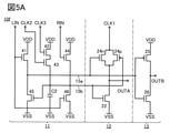
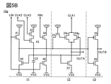
- 5A and 5B are diagrams showing a configuration example of a sequential circuit.
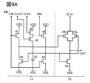
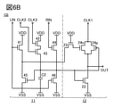
- 6A and 6B are diagrams showing a configuration example of a sequential circuit.
- FIG. 7A is a diagram showing a configuration example of a sequential circuit.
- FIG. 7B is a circuit diagram of a shift register.
- FIG. 7C is a timing chart.
- FIG. 8A is a circuit diagram of a shift register.
- FIG. 8B is a circuit diagram of an inverter circuit.
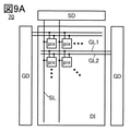
- FIG. 9A is a block diagram of the display device.
- FIG. 9B is a circuit diagram of pixels.
- FIG. 10A is a schematic top view of the inverter circuit.
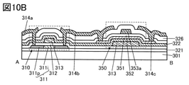
- FIG. 10B is a schematic cross-sectional view of the inverter circuit.
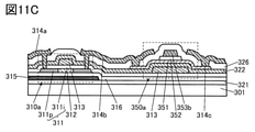
- 11A to 11C are schematic cross-sectional views of the inverter circuit.
- FIG. 12A is a block diagram of the display device. 12B and 12C are circuit diagrams of a pixel circuit.
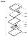
- 13A and 13B are diagrams showing a configuration example of a display module.
- 14A and 14B are diagrams showing a configuration example of an electronic device.
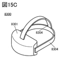
- 15A to 15E are diagrams showing a configuration example of an electronic device.
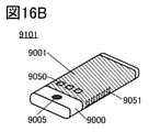
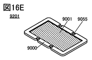
- 16A to 16G are diagrams showing a configuration example of an electronic device.
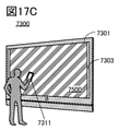
- 17A to 17D are diagrams showing a configuration example of
- a transistor is a type of semiconductor element, and can realize current or voltage amplification and switching operation to control conduction or non-conduction.
- the transistor in the present specification includes an IGFET (Insulated Gate Field Transistor) or a thin film transistor (TFT: Thin Film Transistor) and the like.
- source and drain functions may be interchanged when transistors with different polarities are used, or when the direction of current changes during circuit operation. Therefore, in the present specification, the terms “source” and “drain” may be used interchangeably.
- “electrically connected” includes the case of being connected via "something having some kind of electrical action”.
- the “thing having some kind of electrical action” is not particularly limited as long as it enables the exchange of electric signals between the connection targets.
- “things having some kind of electrical action” include electrodes and wirings, switching elements such as transistors, resistance elements, coils, capacitive elements, and other elements having various functions.
- a node means an element (for example, wiring) that enables electrical connection of elements constituting a circuit. Therefore, the "node to which A is connected” means a wiring that is electrically connected to A and can be regarded as having the same potential as A. Even if one or more elements (for example, switches, transistors, capacitive elements, inductors, resistance elements, diodes, etc.) that enable electrical connection are arranged in the middle of the wiring, they have the same potential as A. , It is assumed that the wiring is a node to which A is connected.
- the display panel which is one aspect of the display device, has a function of displaying (outputting) an image or the like on the display surface. Therefore, the display panel is an aspect of the output device.
- a connector such as FPC (Flexible Printed Circuit) or TCP (Tape Carrier Package) is attached to the board of the display panel, or an IC is used on the board by a COG (Chip On Glass) method or the like.
- FPC Flexible Printed Circuit
- TCP Transmission Carrier Package
- COG Chip On Glass
- FIG. 1A shows a configuration example of the sequential circuit 10 of one aspect of the present invention.
- the sequential circuit 10 includes a circuit 11, a circuit 12, and a circuit 13.
- the circuit 11 has a wiring 15a and a wiring 15b.
- the circuit 11 and the circuit 12 are electrically connected to each other via the wiring 15a and the wiring 15b.
- the circuit 11 and the circuit 13 are electrically connected to each other via the wiring 15a.
- the circuit 11 has a function of outputting a first signal to the wiring 15a and a second signal to the wiring 15b according to the potentials of the signal LIN and the signal RIN. That is, the circuit 11 can also be called a control circuit.
- the second signal is a signal obtained by inverting the first signal. That is, when the first signal and the second signal are signals having two types of potentials, high potential and low potential, respectively, when the high potential is output from the circuit 11 to the wiring 15a, the low potential is output to the wiring 15b. Is output, and when a low potential is output to the wiring 15a, a high potential is output to the wiring 15b.
- the circuit 12 has a function of outputting either the signal CLK or the potential VSS to the output terminal OUTA based on the signals input to the wiring 15a and the wiring 15b.
- the circuit 12 outputs the signal CLK when the wiring 15a has a high potential, and outputs the potential VSS when the wiring 15a has a low potential.
- the circuit 12 can be called an amplifier circuit, a buffer circuit, or the like.
- a clock signal can be used as the signal CLK.
- a signal having a duty ratio (ratio of a period of high level potential in a period of one cycle of the signal) of 45% or more and 55% or less can be preferably used. More preferably, a signal having a duty ratio of 50% can be used as the clock signal.
- the duty ratio of the clock signal is not limited to the above, and can be appropriately changed depending on the driving method.
- the clock signal means that a high potential and a low potential are repeated, and the interval between the rise of the potential and the rise of the next potential, or the fall of the potential and the fall of the next potential.
- the pulse signal means a signal whose potential changes with time.
- the pulse signal includes a signal whose potential changes periodically.
- the pulse signal includes a signal whose potential changes periodically, such as a square wave, a triangular wave, a sawtooth wave, and a sine wave. Therefore, it can be said that the clock signal is one aspect of the pulse signal.
- the potential VDD can be a potential higher than the potential VSS.
- the signal CLK is a signal in which high potential and low potential are alternately applied. At this time, it is preferable that the low potential of the signal CLK is the same potential as the potential VSS.
- a high potential for example, potential VDD may be applied to one of the source and drain of the transistor 21.
- the circuit 13 has a function of outputting either potential VDD or potential VSS to the output terminal OUTB according to the potential of the wiring 15a.
- the circuit 13 outputs the low potential VSS when the wiring 15a has a high potential, and outputs the high potential VDD when the wiring 15a has a low potential. That is, the circuit 13 can output a signal obtained by inverting the first signal to the output terminal OUTB. In other words, the circuit 13 can output a signal similar to the second signal to the output terminal OUTB.
- the circuit 13 can be called an inverter circuit or the like.
- the sequential circuit 10 functions as a flip-flop circuit and can be used as a part of the shift register circuit.
- the sequential circuit 10 can be used as a part of the drive circuit of the display device.
- it can be suitably used as a part of a scanning line drive circuit (also referred to as a gate driver circuit) of a display device.
- a scanning line (also referred to as a gate line) connected to a plurality of pixels of a display device shall be connected to at least one or both of the output terminal OUTA and the output terminal OUTB. Can be done.
- a scanning line also referred to as a gate line
- the circuit 11 has a transistor 31 to a transistor 34. It is preferable to apply an n-channel type transistor to the transistor 31 to the transistor 34.
- Transistor 31 and transistor 34 are selected to be conductive or non-conducting according to the potential of the signal LIN.
- Transistor 32 and transistor 33 are selected to be conductive or non-conducting according to the potential of the signal RIN.
- the transistor 31 When the signal LIN has a high potential and the signal RIN has a low potential, the transistor 31 is in a conductive state and the transistor 33 is in a non-conducting state, and the wiring to which the potential VDD is given and the wiring 15a are electrically connected. Further, the transistor 34 is in a conductive state and the transistor 32 is in a non-conducting state, and the wiring to which the potential VSS is given and the wiring 15b are electrically connected.
- the signal LIN has a low potential and the signal RIN has a high potential
- the conduction and non-conduction states of each transistor are reversed from the above, and the wiring 15a is electrically connected to the wiring to which the potential VSS is given, and the wiring 15b. Is electrically connected to the wiring given the potential VDD.
- the circuit 12 has a transistor 21 and a transistor 22. It is preferable to apply an n-channel type transistor to the transistor 21 and the transistor 22.
- the transistor 21 is electrically connected to the wiring 15a at the gate, the wiring to which the signal CLK is given to one of the source and drain, and the source and drain of the transistor 22 and the output terminal OUTA, respectively.
- Ru is electrically connected to the wiring 15b at the gate and the wiring to which the potential VSS is given to the other of the source and the drain.
- the output terminal OUTA is a portion to which the output potential from the circuit 12 is given, and may be a part of the wiring or a part of the electrode.
- the signal CLK is output to the output terminal OUTA via the transistor 21.
- the potential VSS is output to the output terminal OUTA via the transistor 22.
- the circuit 13 has a transistor 25 and a transistor 26.
- the transistor 25 is preferably a p-channel type transistor (p-type transistor), and the transistor 26 is preferably an n-channel type transistor (n-type transistor).
- the transistor 25 is electrically connected to the wiring 15a at the gate, the wiring to which one of the source and the drain is given the potential VDD, the other from the source and the drain of the transistor 26, and the output terminal OUTB, respectively. Will be done.
- the transistor 26 is electrically connected to the wiring 15a at the gate and the wiring to which the potential VSS is given to the other of the source and the drain.
- the output terminal OUTB is a portion to which the output potential from the circuit 13 is given, and may be a part of the wiring or a part of the electrodes.
- the potential VSS is output to the output terminal OUTB via the transistor 26.
- the potential VDD is output to the output terminal OUTB via the transistor 25.
- FIG. 1B is a timing chart showing an example of a driving method of the sequential circuit 10.
- FIG. 1B schematically shows the time change of the potential in the signal LIN, the signal RIN, the signal CLK, the output terminal OUTA, and the output terminal OUTB.
- both the signal LIN and the signal RIN have low potentials.
- a low potential is output to the output terminal OUTA and a high potential is output to the output terminal OUTB regardless of the potential of the signal CLK.
- the signal LIN becomes high potential. Further, it is assumed that the signal CLK has a low potential during the period T1-T2. As a result, in the period T1-T2, the signal CLK (that is, low potential) is output to the output terminal OUTA, and the low potential is output to the output terminal OUTB.
- the signal LIN becomes low potential.
- all four transistors in the circuit 11 are turned off, so that the potentials of the wiring 15a and the wiring 15b are maintained.
- the signal CLK changes to a high potential at time T2.
- the high potential is output to the output terminal OUTA, and the low potential is continuously output to the output terminal OUTB.
- the signal RIN becomes high potential.
- the wiring 15a has a low potential and the wiring 15b has a high potential. Therefore, in the period T3-T4, a low potential is given to the output terminal OUTA and a high potential is given to the output terminal OUTB.
- the signal RIN becomes low potential.
- all the transistors in the circuit 11 are turned off, and the potentials of the wiring 15a and the wiring 15b are maintained. Therefore, after the time T4, a low potential is output to the output terminal OUTA and a high potential is output to the output terminal OUTB.
- both the signal LIN and the signal RIN have low potentials before the time T1 and after the time T4, it can be said that the sequential circuit 10 is in the standby state (also referred to as the non-operating state or the non-selected state). .. During this period, a low potential is output to the output terminal OUTA and a high potential is output to the output terminal OUTB.
- the signal output to the output terminal OUTA has a high potential only during the period T2-T3, and is a signal that always has a low potential during the other periods. That is, the signal output to the output terminal OUTA of the sequential circuit 10 can be said to be a Normally Low signal.
- the signal output to the output terminal OUTB is a signal having a low potential only during the period T1-T3 and always having a high potential during the other periods. That is, the signal output to the output terminal OUTB can be said to be a Normally High signal.
- the sequential circuit 10 can output two types of signals, normally low and normally high, when the sequential circuit 10 is used, for example, in a scanning line drive circuit of a display device, the pixels of the display device are displayed. It can be driven by the two types of signals. Therefore, a multifunctional display device can be realized.
- the n-channel type transistor constituting the sequential circuit 10 it is preferable to use a transistor to which an oxide semiconductor is applied to the semiconductor layer on which the channel is formed.
- the leakage current flowing between the source and the drain in the off state is significantly lower than that of the transistor to which silicon is applied.
- the p-channel type transistor constituting the sequential circuit 10 it is preferable to use a transistor having silicon in the semiconductor layer on which the channel is formed.
- silicon examples include single crystal silicon, polycrystalline silicon, and amorphous silicon.
- the LTPS transistor has high field effect mobility and good frequency characteristics. Further, since the LTPS transistor has a large current that can be passed in the ON state, the time required for charging and discharging the wiring connected to the output terminal OUTB can be shortened.
- CMOS Complementary Metal Oxide Semiconductor
- FIG. 1C shows, as an example, a schematic cross-sectional view of a sequential circuit 10 including a cross section of the transistor 25 and the transistor 26 in the channel length direction of the circuit 13.
- FIG. 1C shows an example in which a so-called top gate type transistor in which a gate electrode is provided above the semiconductor layer is applied as the transistor 25 and the transistor 26.
- the transistor configuration is not limited to this.
- the transistor 25 has a semiconductor layer 51, a gate insulating layer 52, and a gate electrode 53.
- the semiconductor layer 51 contains polycrystalline silicon.
- the semiconductor layer 51 has a pair of low resistance regions 51p that sandwich the channel forming region and exhibit p-type conductivity.
- the transistor 26 has a semiconductor layer 56, a gate insulating layer 57, and a gate electrode 58.
- the semiconductor layer 56 contains a metal oxide.
- the semiconductor layer 56 has a pair of low resistance regions 56n that sandwich the channel forming region and exhibit n-type conductivity.
- the semiconductor layer 51 of the transistor 25 is provided on the insulating layer 60. Further, the insulating layer 61 is provided so as to cover the transistor 25, and the insulating layer 62 and the insulating layer 63 are laminated on the insulating layer 61.
- the semiconductor layer 56 of the transistor 26 is provided in contact with the upper surface of the insulating layer 63. Further, an insulating layer 64 is provided so as to cover the transistor 26.
- a conductive layer 54a, a conductive layer 54b, and a conductive layer 54c are provided on the insulating layer 64.
- a part of the conductive layer 54a corresponds to a wiring to which the potential VDD is given.
- a part of the conductive layer 54c corresponds to the wiring to which the potential VSS is given.
- a part of the conductive layer 54b corresponds to the output terminal OUTB.
- the gate electrode 53 and the gate electrode 58 are electrically connected in a region (not shown).
- the conductive layer 54a and the conductive layer 54b are electrically connected to the low resistance region 51p at the openings provided in the insulating layer 64, the insulating layer 63, the insulating layer 62, and the insulating layer 61, respectively.
- the conductive layer 54b and the conductive layer 54c are electrically connected to the low resistance region 56n at the openings provided in the insulating layer 64, respectively.
- the semiconductor layer 51 and its surroundings are included in the manufacturing process. It may contain a hydrogen atom, a hydrogen molecule, or a compound containing hydrogen (such as water).
- hydrogen is an element that can be a carrier supply source, so it is preferable to reduce the hydrogen concentration in and around the semiconductor layer 56 of the transistor 26 as much as possible.
- oxygen deficiency can also be a factor of a carrier supply source, so that it is preferable that the semiconductor layer 56 of the transistor 26 is provided with an oxide having reduced hydrogen in contact with it.
- the semiconductor layer 51 of the transistor 25 and the semiconductor layer 56 of the transistor 26 are separated by an insulating layer 62 having a barrier property against hydrogen and water. Further, the semiconductor layer 56 of the transistor 26 is preferably provided in contact with the insulating layer 63 containing an oxide. At this time, the insulating layer 62 has at least a material having a lower permeability to hydrogen and water (difficult to permeate hydrogen and water) than the insulating layer 61 and the insulating layer 63.
- the insulating layer 62 an inorganic insulating film containing silicon nitride, silicon nitride oxide, aluminum oxide, or hafnium oxide can be used.
- an oxide film such as silicon oxide or silicon oxynitride can be used. At this time, the insulating layer 63 is preferably a film in which oxygen is released by heating.
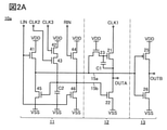
- FIG. 2A shows a configuration example of the sequential circuit 10a.
- the sequential circuit 10a is mainly different in the configurations of the circuit 11 and the circuit 12 as compared with the sequential circuit 10. Since the circuit 13 has the same configuration as the above-mentioned sequential circuit 10, the description thereof will be omitted.
- the circuit 11 has a transistor 41 to a transistor 46 and a capacitance C2. Further, a signal LIN, a signal CLK2, a signal CLK3, and a signal RIN are input to the circuit 11.
- the circuit 12 has a transistor 21, a transistor 22, a transistor 23, and a capacitance C1. Further, the signal CLK1 is input to the circuit 12.
- circuit 11 and the circuit 13 are supplied with a high potential potential VDD and a low potential potential VSS.
- n-channel type transistor it is preferable to apply the above-mentioned n-channel type transistor to the transistor 41 to 46 and the transistor 21 to 23.
- the circuit 11 has a function of outputting a first signal to the wiring 15a and a second signal obtained by inverting the first signal to the wiring 15b according to various input signals.
- the transistor 41 has a wiring in which the gate is given a signal LIN, a wiring in which one of the source and the drain is given the wiring 15a, and one of the source and drain of the transistor 45, and the other is a wiring in which the potential VDD is given. It is electrically connected.
- the transistor 42 is electrically connected to a wiring in which the gate is given the signal CLK3, one of the source and drain of the transistor 43 is one of the source and drain of the transistor 43, and the other is a wiring to which the potential VDD is given.
- the gate is electrically connected to the wiring to which the signal CLK2 is given, and the other of the source and the drain is electrically connected to the wiring 15b, one electrode of the capacitance C2, and the gate of the transistor 45, respectively.
- the gate is electrically connected to the wiring to which the signal RIN is given, one of the source and the drain to the wiring 15b, and the other to the wiring to which the potential VDD is given.
- the other of the source and the drain is electrically connected to the wiring to which the potential VSS is given.
- the gate is electrically connected to the wiring to which the signal LIN is given, one of the source and the drain to the wiring 15b, and the other to the wiring to which the potential VSS is given.
- the other electrode is electrically connected to the wiring to which the potential VSS is given.
- the circuit 12 included in the sequential circuit 10a has a configuration in which the transistor 23 and the capacitance C1 are added to the configuration shown in FIG. 1A.
- the gate is electrically connected to the wiring to which the potential VDD is given
- one of the source and the drain is electrically connected to the wiring 15a
- the other is electrically connected to the gate of the transistor 21.
- one electrode is electrically connected to the gate of the transistor 21, and the other electrode is electrically connected to the other of the source and drain of the transistor 21, respectively.
- One of the source and drain of the transistor 21 is electrically connected to the wiring to which the signal CLK1 is given.
- the potential of the gate of the transistor 21 rises to a potential close to twice the potential VDD, for example, the potential VDD can be output to the output terminal OUTA without being affected by the threshold voltage of the transistor 21. .. As a result, it is possible to realize a sequential circuit 10a having high output performance without increasing the types of power supply potentials.
- the transistor 23 is turned off, so that the gate of the transistor 21 and the wiring 15a are electrically separated from each other, and the transistor 22 is in a state of being electrically separated.
- the gate becomes floating.
- the potential of the wiring 15a does not rise from the output potential of the circuit 12 when the transistor 23 is turned off, the potential of the transistor or the like in the circuit 12 is higher than the output potential via the wiring 15a. Can be prevented from being applied. Thereby, the reliability of the sequential circuit 10a can be improved.
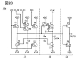
- FIG. 2B shows a configuration example of the sequential circuit 10b.
- the sequential circuit 10b is different from the sequential circuit 10a in that the transistor configuration is different.
- a transistor having a back gate is applied to the n-channel type transistor included in the circuit 11, the circuit 12, and the circuit 13.
- the back gate of the transistor 45 and the transistor 22 is electrically connected to the wiring to which the potential VSS is given. That is, the transistor 45 and the transistor 22 have a configuration in which the back gate is electrically connected to the source.
- the period in which the wiring 15b has a high potential is significantly longer than the period in which the wiring 15b has a low potential. Therefore, the transistor 45 and the transistor 22 in which the gate is connected to the wiring 15b are in the on state for a significantly longer period than in the off state. Therefore, the transistor 45 and the transistor 22 are more likely to have a fluctuation in the threshold voltage than other transistors. Specifically, the threshold voltage of the transistor tends to shift in the positive direction.
- the transistor 45 and the transistor 22 are configured to electrically connect one of the pair of gates having a semiconductor layer sandwiched between them to a wiring to which a low potential is given (a wiring to which a potential VSS is given). And. With such a configuration, it is possible to suitably suppress the threshold voltage of the transistor 45 and the transistor 22 from shifting in the positive direction. Therefore, the reliability of the sequential circuit 10b, and thus the semiconductor device, the display device, the electronic device, and the like using the sequential circuit 10b can be improved.
- the transistor 45 and the transistor 22 are configured such that one of the gates and the source is electrically connected, so that it is possible to preferably prevent the threshold voltage from becoming a negative value. That is, it becomes easy to make the transistor 45 and the transistor 22 have normal off characteristics. Further, the transistor 45 and the transistor 22 also have an effect of increasing saturation by having a configuration in which one of the gates and the source is electrically connected. This facilitates the design of the circuit 11 and the circuit 12, and makes it possible to realize a circuit that can operate stably.
- a transistor in which a pair of gates are electrically connected to each other is applied to an n-channel type transistor other than the transistor 45 and the transistor 22.
- the wiring 15b is given a potential obtained by inverting the potential of the wiring 15a.
- the circuit 13 can output a signal in which the potential of the wiring 15a is inverted to the output terminal OUTB. Therefore, the configuration of the circuit 11 can be simplified by supplying (feeding back) the output potential of the output terminal OUTB to the wiring 15b.
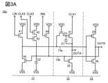
- FIG. 3A shows a configuration example of the sequential circuit 10c.
- the configuration of the sequential circuit 10c is mainly different from that of the sequential circuit 10a. Specifically, in the sequential circuit 10c, the wiring 15b and the output terminal OUTB of the circuit 13 are electrically connected. Further, in the sequential circuit 10c, as compared with the sequential circuit 10a, the transistor 46 which functions as a switch for controlling the continuity and non-conduction between the wiring 15b and the potential VSS is omitted.
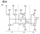
- FIG. 3B shows a configuration example of the sequential circuit 10d.
- the transistor 42, the transistor 43, and the capacitance C2 are further omitted from the sequential circuit 10c. That is, the circuit 11 is composed of a transistor 41, a transistor 44, and a transistor 45.
- one or more of the transistor 42, the transistor 43, the transistor 44, and the transistor 46 can be omitted from the configuration of the sequential circuit 10a.
- FIG. 4 shows a configuration example of the sequential circuit 10e having a configuration different from the above.
- the positions of the circuit 12 and the circuit 13 are interchanged with those described above for easy viewing.
- the circuit 11 has a transistor 41, a transistor 46, and a transistor 47.
- the transistor 47 is electrically connected to a wire to which the signal RES is given at the gate, a wire 15a to which one of the source and the drain is given, and a wire to which the potential VSS is given to the other.
- a signal for controlling the reset operation of the sequential circuit 10e is given to the signal RES, for example.
- the gates of the transistor 25 and the transistor 26 are electrically connected to the wiring 15a, respectively. Further, the output terminal OUTB and the wiring 15b are electrically connected.
- the circuit 12 has a transistor 21, a transistor 22, and a capacitance C1.
- the gate is electrically connected to the wiring 15a, one of the source and the drain is electrically connected to the wiring to which the signal CLK1 is given, and the other is electrically connected to the output terminal OUTA.
- the gate is electrically connected to the wiring 15b, one of the source and the drain is electrically connected to the output terminal OUTA, and the other is electrically connected to the wiring to which the potential VSS is given.
- the capacitance C1 one electrode is electrically connected to the wiring 15a and the gate of the transistor 21, and the other electrode is electrically connected to the output terminal OUTA.
- the output signal to the output terminal OUTA and the output terminal OUTB is held even after the signal LIN is given a high potential and then changes to a low potential. Further, when a high potential is applied to the signal RES and the transistor 47 becomes conductive, a low potential VSS can be supplied to the wiring 15a and the state of the sequential circuit 10e can be reset.
- FIG. 5A shows a configuration example of the sequential circuit 10f having a configuration different from the above.
- the sequential circuit 10f is mainly different from the sequential circuit 10a in that the configuration of the circuit 12 is different.
- the circuit 12 has a transistor 22, a transistor 24n, and a transistor 24p.
- the transistor 24n is an n-channel type transistor
- the transistor 24p is a p-channel type transistor.
- the transistor 24n and the transistor 24p are electrically connected to one of the source and drain and the other to form a so-called analog switch.
- the gate of the transistor 24n is electrically connected to the wiring 15a
- the gate of the transistor 24p is electrically connected to the wiring 15b.
- the analog switch is in a non-conducting state, the transistor 22 is in a conducting state, and the wiring to which the potential VSS is given and the output terminal OUTA are conducted.
- the p-channel type transistor can be applied not only to the circuit 13 but also to other circuits.
- a p-channel type transistor is applied to the circuit 12 is shown, but it can also be applied to the circuit 11.
- the configuration of the circuit 11 and the circuit 13 is the same as that of the sequential circuit 10a, the configuration is not limited to this, and various configurations exemplified above can be applied. For example, by electrically connecting the output terminal OUTB of the circuit 13 and the wiring 15b, a part of the transistors of the circuit 11 can be omitted and the circuit can be simplified.
- FIG. 5B shows a sequential circuit 10g having a partially different configuration from the above.
- the sequential circuit 10g further includes a transistor 23 in the circuit 12.
- a potential VDD is given to the gate of the transistor 23, and one of the source and the drain is electrically connected to the wiring 15a and the other is electrically connected to the gate of the transistor 24n.
- the capacitance C1 may be provided between the gate of the transistor 24n and the output terminal OUTA, as in the above-mentioned sequential circuit 10a.
- the sequence circuit 10h shown in FIG. 6A is an example in which the circuit 13 in the sequence circuit 10f is omitted.
- the sequential circuit 10h can output the signal CLK1 or the potential VSS from the output terminal OUT.
- the sequential circuit 10i shown in FIG. 6B is an example in which the transistor 23 is added to the circuit 12 of the sequential circuit 10h.
- the transistor having the back gate exemplified in the sequential circuit 10b may be applied to the n-channel type transistor. At this time, it is preferable to select and use a transistor in which a pair of gates are electrically connected, a transistor in which one gate is electrically connected to a source, or a transistor having no back gate.
- FIG. 7A is a diagram illustrating input / output terminals of the sequential circuit 30.
- the sequential circuit 30 has a terminal to which a signal LIN, a signal RIN, a signal CLK1, a signal CLK2, and a signal CLK3 are input as input terminals, and an output terminal OUTA and an output terminal OUTB as output terminals.
- the sequential circuit 30 for example, the sequential circuit 10a, the sequential circuit 10b, the sequential circuit 10c, or the like can be used.
- FIG. 7B shows a configuration example of the drive circuit 40.
- the drive circuit 40 has a plurality of sequential circuits 30.
- FIG. 7B shows the sequential circuit 30_1 to the sequential circuit 30_1.
- the sequential circuit located at the nth position from the side closer to the input of the drive circuit 40 will be referred to as a sequential circuit 30_n (n is an integer of 1 or more).
- any three of the signals CK1 and CK4 are used as the signal CLK1, the signal CLK2, and the signal CLK3.
- the combination of the signal CK1 to the signal CK4 is the same for every four stages. That is, the same signal is input to the sequential circuit 30_n and the sequential circuit 30_n + 4 as the signal CLK1, the signal CLK2, and the signal CLK3.
- wiring OUTAn and wiring OUTBn which are output wirings, are connected to the output terminal OUTA and the output terminal OUTB of the sequential circuit 30_n, respectively.
- a signal SP is input to the sequential circuit 30_1 as a signal LIN. Further, the signal of the output terminal OUTA of the sequence circuit 30_n-1 in the previous stage is input as the signal LIN to the sequence circuit 30_n having n of 2 or more. Further, the signal of the output terminal OUTA of the sequential circuit 30_n + 2 is input to the sequential circuit 30_n as the signal RIN.
- the sequential circuit 30_1 receives the signals of the signal CK1, the signal CK2, the signal CK3, the signal SP, and the output terminal OUTA of the sequential circuit 30_1, and outputs the output signal to the wiring OUTA1 and the wiring OUTB1. Further, the sequential circuit 30_2 is input with a signal CK2, a signal CK3, a signal CK4, a signal of the output terminal OUTA of the sequential circuit 30_1, and a signal of the output terminal OUTA of the sequential circuit 30_1, and outputs an output signal to the wiring OUTA2 and the wiring OUTB2. do.
- FIG. 7C shows a timing chart related to the driving method of the driving circuit 40.
- FIG. 7C shows the time change of the potential for each of the signal SP, the signals CK1 to CK4, the wiring OUTA1 to the wiring OUTA6, and the wiring OUTB1 to the wiring OUTB6 from the top.
- the signal SP has a high potential and the signal CK1 has a low potential.
- a low potential is output to the wiring OUTA1 to the wiring OUTA6, and a high potential is output to the wiring OUTB2 to the wiring OUTB6.
- the signal SP becomes high potential, a low potential is output to the wiring OUTB1.
- the signals CK1 to CK4 are clock signals shifted by a quarter cycle, respectively. Therefore, as shown in FIG. 7C, signals such as the signal CK1 that are deviated by a quarter cycle are output to the wiring OUTA1 to the wiring OUTA6 and the wiring OUTB1 to the wiring OUTB6.
- FIG. 8A shows a configuration example of the drive circuit 40a having a partially different configuration from the above.
- a signal CK1 and a signal CK2 are given to the drive circuit 40a as clock signals. Further, the drive circuit 40a has a plurality of inverter circuits 80.
- Either signal CK1 or signal CK2 is input to the input terminal of the inverter circuit 80, and the inverted signal is output from the output terminal. Since the two inverted signals are signals that are deviated from the signal CK1 and the signal CK2 by half a cycle, they are the same signals as the signal CK3 and the signal CK4 in the above configuration example 1.
- FIG. 8A a pair of inverter circuits 80 are provided for every four sequential circuits 30_n. More specifically, three sequential circuits 30 are connected to one inverter circuit 80. By reducing the number of sequential circuits connected to one inverter circuit 80 in this way, the output capacity required for the inverter circuit 80 can be reduced, and the circuit scale can be reduced.
- FIG. 8B shows an example of a configuration applicable to the inverter circuit 80.
- the inverter circuit 80 has the same configuration as the circuit 13, and includes a p-channel type transistor 81 and an n-channel type transistor 82. As shown in FIG. 8B, for example, when the clock signal CK is input to the inverter circuit 80, the inverted clock signal CKB in which the clock signal CK is inverted can be output.
- the configuration of the drive circuit is not limited to this, and the signal, wiring, etc. can be appropriately changed according to the configuration of the sequential circuit to be used. For example, by using a sequential circuit having a small number of input signals, such as the sequential circuit 10d and the sequential circuit 10e, one or both of the wiring and the signal can be reduced, and the drive circuit can be simplified.
- Display device configuration example Hereinafter, a configuration example of a display device to which the drive circuit of one aspect of the present invention can be applied will be described.
- FIG. 9A shows a block diagram of the display device 70.
- the display device 70 includes a display unit DI, a pair of drive circuits GD, and a drive circuit SD.
- a plurality of pixel pix are arranged in a matrix on the display unit DI.
- Each pixel pix has one or more display elements and one or more transistors.
- the drive circuit GD functions as a gate line drive circuit (also referred to as a scanning line drive circuit or a gate driver).
- the drive circuit SD functions as a source line drive circuit (also referred to as a signal line drive circuit or a source driver).
- the pixel pix located in the odd-numbered rows is electrically connected to one drive circuit GD, and the pixel pix located in the even-numbered rows is electrically connected to the other drive circuit.
- the occupied area of each drive circuit GD can be reduced, and a narrow frame display device can be realized.
- the drive circuit GD and the pixel pix are electrically connected via the scanning line GL1 and the scanning line GL2. Further, the drive circuit SD and the pixel pix are electrically connected to each other via the signal line SL.
- the output signal of the output terminal OUTA of the sequential circuit exemplified above is given to the scanning line GL1. Further, the output signal of the output terminal OUTB is given to the scanning line GL2. Therefore, the scanning line GL1 is always given a high potential at the time of selection and a low potential at the time of non-selection. On the other hand, the scanning line GL2 is always given a low potential at the time of selection and a high potential at the time of non-selection.
- FIG. 9B shows an example of pixel pix.
- the pixel pix is an example in which a light emitting element is applied as a display element.
- the pixel pix has a transistor 71, a transistor 72, a transistor 73, a light emitting element 74, and a capacitance CS.
- the transistor 71 functions as a selection transistor.
- the transistor 72 functions as a drive transistor for controlling the current flowing through the light emitting element 74.
- the transistor 73 has a function of cutting off the current flowing through the light emitting element 74.
- the transistor 71 and the transistor 73 are n-channel type transistors, and the transistor 72 is a p-channel type transistor.
- the gate is electrically connected to the scanning line GL1
- one of the source and drain is electrically connected to the signal line SL
- the other is electrically connected to the gate of the transistor 72
- one electrode of the capacitance CS In the transistor 72, one of the source and the drain is electrically connected to the other electrode of the wiring AL and the capacitance CS, and the other is electrically connected to one of the source and the drain of the transistor 73, respectively.
- the gate is electrically connected to the scanning line GL2, and the other of the source and the drain is electrically connected to one of the electrodes of the light emitting element 74.
- the other electrode of the light emitting element 74 is electrically connected to the wiring CL.
- the wiring AL is given an anode potential
- the wiring CL is given a cathode potential lower than the anode potential.
- the transistor 71 becomes a non-conducting state. Further, since a high potential is applied to the scanning line GL2, the transistor 73 becomes conductive, and a current corresponding to the gate potential of the transistor 72 flows through the transistor 73 to the light emitting element 74.
- the configuration of the pixel fix is not limited to this, and various configurations can be used.
- the scanning line GL1 and the scanning line GL2 each have at least a transistor to which a gate is connected.
- Transistor configuration example Hereinafter, more specific configuration examples of transistors that can be applied to the sequential circuit, the drive circuit, the display device, and the like exemplified above will be described.
- an inverter circuit composed of a transistor having polycrystalline silicon in the channel forming region (LTPS transistor) and a transistor having an oxide semiconductor in the channel forming region (OS transistor) will be described as an example.
- FIG. 10A shows a schematic top view of the inverter circuit.
- the inverter circuit has a transistor 310 and a transistor 350.
- the transistor 310 is an LTPS transistor, and the transistor 350 is an OS transistor.
- the transistor 310 can be applied to the transistor 25 and the like exemplified above. Further, the transistor 350 can be applied to the transistor 26 and the like exemplified above.
- the OS transistor a transistor using an oxide semiconductor in the semiconductor layer on which the channel is formed can be used.
- the semiconductor layers include, for example, indium and M (M is gallium, aluminum, silicon, boron, yttrium, tin, copper, vanadium, berylium, titanium, iron, nickel, germanium, zirconium, molybdenum, lanthanum, cerium, neodymium, etc. It is preferred to have one or more selected from hafnium, tantalum, tungsten, and gallium) and zinc.
- M is preferably one or more selected from aluminum, gallium, yttrium, and tin.
- an oxide containing indium, gallium, and zinc also referred to as IGZO
- a transistor using an oxide semiconductor having a wider bandgap and a smaller carrier density than silicon can realize an extremely small off-current. Therefore, due to the small off-current, it is possible to retain the charge accumulated in the capacitance connected in series with the transistor for a long period of time.
- a part of the conductive layer 313 shown in FIG. 10A functions as an input terminal IN.
- a part of the conductive layer 314b functions as a part of the output terminal OUT.
- a part of the conductive layer 314c functions as a wiring to which the potential VSS is given.
- a part of the conductive layer 314d functions as a wiring to which the potential VDD is given.
- FIG. 10A shows an example having six transistors 310 connected in parallel and four transistors 350 connected in parallel.
- heat generation due to current can be reduced by using transistors with relatively small channel lengths in parallel instead of using one transistor with a large channel width, and circuit reliability. Can be improved.
- FIG. 10B is a schematic cross-sectional view taken along the alternate long and short dash line AB in FIG. 10A.
- FIG. 10B shows a cross section of the transistor 310 and the transistor 350 in the channel length direction.
- An insulating layer 321 is provided on the substrate 301, and a transistor 310 and a transistor 350 are provided on the insulating layer 321.
- the transistor 310 has a semiconductor layer 311 and an insulating layer 312 that covers the semiconductor layer 311 and a conductive layer 313 that is located on the insulating layer 312 and overlaps with the semiconductor layer 311. Further, an insulating layer 322 covering the conductive layer 313 and the insulating layer 312, an insulating layer 352 on the insulating layer 322, and an insulating layer 326 on the insulating layer 352 are provided.
- the semiconductor layer 311 contains polycrystalline silicon.
- the semiconductor layer 311 has a channel forming region 311i and a pair of low resistance regions 311p sandwiching the channel forming region 311i.
- a part of the insulating layer 312 functions as a gate insulating layer of the transistor 310.
- a part of the conductive layer 313 functions as a gate electrode of the transistor 310.
- the insulating layer 322 preferably has a laminated structure in which a first insulating film having a barrier property against hydrogen and water and a second insulating film containing an oxide are laminated.
- the first insulating film corresponds to the insulating layer 62 exemplified in FIG. 1C and the like
- the second insulating film corresponds to the insulating layer 63.
- the above description can be used as the material and the like that can be used for the first insulating film and the second insulating film.
- the low resistance region 311p is a region containing an impurity element.
- the transistor 310 is an n-channel type transistor, phosphorus or arsenic may be added to the low resistance region 311p.
- boron, aluminum or the like may be added to the low resistance region 311p.
- the transistor 310 is a p-channel type transistor.
- the above-mentioned impurities may be added to the channel formation region 311i.
- the transistor 350 is located on the conductive layer 313 on the insulating layer 312, the insulating layer 322 covering the conductive layer 313, the semiconductor layer 351 on the insulating layer 322, the insulating layer 352 covering the semiconductor layer 351 and the insulating layer 352. It also has a conductive layer 353a that overlaps with the semiconductor layer 351. Further, the insulating layer 326 is provided so as to cover the insulating layer 352 and the conductive layer 353a.
- the semiconductor layer 351 includes an oxide semiconductor.
- the region overlapping with either or both of the conductive layer 353a and the conductive layer 313 of the semiconductor layer 351 functions as a channel forming region.
- a part of the insulating layer 322 functions as a back gate insulating layer (second gate insulating layer) of the transistor 350.
- a part of the insulating layer 352 functions as a gate insulating layer (first gate insulating layer) of the transistor 350.
- the other part of the conductive layer 313 functions as a back gate electrode (second gate electrode) of the transistor 350.
- a part of the conductive layer 353a functions as a gate electrode (first gate electrode) of the transistor 350.
- a conductive layer 314a, a conductive layer 314b, and a conductive layer 314c are provided on the insulating layer 326.
- the conductive layer 314a and the conductive layer 314b are provided in the insulating layer 326, the insulating layer 352, the insulating layer 322, and the insulating layer 312, and are electrically connected to the low resistance region at the opening reaching the low resistance region 311p. ..
- the conductive layer 314b and the conductive layer 314c are provided in the insulating layer 326 and the insulating layer 352, and are electrically connected to the semiconductor layer 351 at the opening reaching the semiconductor layer 351.
- the conductive layer 313 also serves as a gate electrode of the transistor 310 and a back gate electrode of the transistor 350.
- the conductive layer 353a and the conductive layer 313 are electrically connected to each other at the opening shown by the broken line, and the same potential input from the input terminal IN is given to them.
- FIG. 11A shows an example in which a transistor 310a having a pair of gate electrodes is applied instead of the transistor 310.
- the transistor 310a is mainly different from the transistor 310 in that it has a conductive layer 315 and an insulating layer 316.
- the conductive layer 315 is provided on the insulating layer 321. Further, the insulating layer 316 is provided so as to cover the conductive layer 315 and the insulating layer 321.
- the semiconductor layer 311 is provided so that at least the channel forming region 311i overlaps with the conductive layer 315 via the insulating layer 316.
- a part of the conductive layer 313 functions as a first gate electrode, and a part of the conductive layer 315 functions as a second gate electrode.
- a part of the insulating layer 312 functions as the first gate insulating layer, and a part of the insulating layer 316 functions as the second gate insulating layer.
- the conductive layer 313 and the conductive layer 313 are conducted through the openings provided in the insulating layer 312 and the insulating layer 316 in a region (not shown).
- the layer 315 may be electrically connected.
- the conductive layer is provided through the openings provided in the insulating layer 322, the insulating layer 312, and the insulating layer 316 in a region (not shown).
- the conductive layer 315 may be electrically connected to the conductive layer 314a or the conductive layer 314a.
- FIG. 11B shows an example in which the transistor 350a is applied instead of the transistor 350 in FIG. 10B.
- the transistor 350a is mainly different in that the shape of the insulating layer 352 is different.
- the insulating layer 352 is processed using the same resist mask as the conductive layer 353b.
- the surface of the region of the semiconductor layer 351 that is not covered by the insulating layer 352 is in contact with the insulating layer 326.
- more carriers may be present than in the channel forming region, so that the electrical resistance can be suitably reduced.
- FIG. 11B shows an example in which the end portion of the conductive layer 353b is located inside the end portion of the insulating layer 352.
- the semiconductor layer 351 can be provided with a relatively high resistance region between the channel forming region and the low resistance region. That is, since the LDD (Lightly Doped Drain) structure is realized, the reliability can be improved.
- the end portion of the conductive layer 353b and the end portion of the insulating layer 352 may be substantially matched, and the insulating layer 352 and the conductive layer 353b may be processed so as to substantially match the top surface shapes. ..
- the top surface shapes are substantially the same.
- the contours do not overlap, and the upper layer may be located inside the lower layer, or the upper layer may be located outside the lower layer. In this case as well, it is said that the top surface shapes are roughly the same.
- FIG. 11C shows an example in which the transistor 310a and the transistor 350a are applied. The above description can be incorporated for the configurations of the transistor 310a and the transistor 350a.
- a metal oxide having nitrogen may also be collectively referred to as a metal oxide.
- the metal oxide having nitrogen may be referred to as a metal oxynitride.
- a metal oxide having nitrogen such as zinc oxynitride (ZnON) may be used for the semiconductor layer.
- CAAC c-axis aligned crystal
- CAC Cloud-Aligned Complex
- CAC Cloud-Aligned Complex
- OS Oxide Semiconductor
- the CAC-OS or CAC-metal oxide has a conductive function in a part of the material, an insulating function in a part of the material, and a semiconductor function as a whole of the material.
- the conductive function is the function of allowing electrons (or holes) to be carriers to flow
- the insulating function is the function of allowing electrons (or holes) to be carriers. It is a function that does not shed.
- CAC-OS or CAC-metal oxide has a conductive region and an insulating region.
- the conductive region has the above-mentioned conductive function
- the insulating region has the above-mentioned insulating function.
- the conductive region and the insulating region may be separated at the nanoparticle level. Further, the conductive region and the insulating region may be unevenly distributed in the material. In addition, the conductive region may be observed with the periphery blurred and connected in a cloud shape.
- CAC-OS or CAC-metal oxide when the conductive region and the insulating region are dispersed in the material in a size of 0.5 nm or more and 10 nm or less, preferably 0.5 nm or more and 3 nm or less, respectively. There is.
- CAC-OS or CAC-metal oxide is composed of components having different band gaps.
- CAC-OS or CAC-metal oxide is composed of a component having a wide gap due to an insulating region and a component having a narrow gap due to a conductive region.
- the carrier when the carrier is flown, the carrier mainly flows in the component having a narrow gap.
- the component having a narrow gap acts complementarily to the component having a wide gap, and the carrier flows to the component having a wide gap in conjunction with the component having a narrow gap. Therefore, when the CAC-OS or CAC-metal oxide is used in the channel forming region of the transistor, a high current driving force, that is, a large on-current and a high field effect mobility can be obtained in the ON state of the transistor.
- CAC-OS or CAC-metal oxide can also be referred to as a matrix composite material (matrix composite) or a metal matrix composite material (metal matrix composite).
- Oxide semiconductors are divided into single crystal oxide semiconductors and other non-single crystal oxide semiconductors.
- non-single crystal oxide semiconductor include CAAC-OS (c-axis aligned crystalline oxide semiconductor), polycrystal oxide semiconductor, nc-OS (nanocrystalline oxide semiconductor), and pseudoamorphous oxide semiconductor (a-lik).
- OS amorphous-like oxide semiconductor), amorphous oxide semiconductors, and the like.
- CAAC-OS has a c-axis orientation and has a crystal structure in which a plurality of nanocrystals are connected in the ab plane direction and have strain.
- the strain refers to a region where the orientation of the lattice arrangement changes between a region in which the lattice arrangement is aligned and a region in which another lattice arrangement is aligned in the region where a plurality of nanocrystals are connected.
- Nanocrystals are basically hexagons, but they are not always regular hexagons and may be non-regular hexagons. Further, in the strain, it may have a lattice arrangement such as a pentagon and a heptagon.
- a lattice arrangement such as a pentagon and a heptagon.
- CAAC-OS it is difficult to confirm a clear grain boundary (also referred to as grain boundary) even in the vicinity of strain. That is, it can be seen that the formation of grain boundaries is suppressed by the distortion of the lattice arrangement. This is because CAAC-OS can tolerate distortion due to the fact that the arrangement of oxygen atoms is not dense in the ab plane direction, or that the bond distance between atoms changes due to the replacement of metal elements. Because.
- CAAC-OS is a layered crystal in which a layer having indium and oxygen (hereinafter, In layer) and a layer having elements M, zinc, and oxygen (hereinafter, (M, Zn) layer) are laminated. It tends to have a structure (also called a layered structure). Indium and the element M can be replaced with each other, and when the element M of the (M, Zn) layer is replaced with indium, it can be expressed as a (In, M, Zn) layer. Further, when the indium of the In layer is replaced with the element M, it can also be expressed as a (In, M) layer.
- CAAC-OS is a highly crystalline metal oxide.
- CAAC-OS it is difficult to confirm a clear grain boundary, so it can be said that the decrease in electron mobility due to the crystal grain boundary is unlikely to occur.
- CAAC-OS is a metal having few impurities and defects (oxygen deficiency (VO: oxygen vacancy), etc.). It can also be called an oxide. Therefore, the metal oxide having CAAC-OS has stable physical properties. Therefore, the metal oxide having CAAC-OS is resistant to heat and has high reliability.
- nc-OS has periodicity in the atomic arrangement in a minute region (for example, a region of 1 nm or more and 10 nm or less, particularly a region of 1 nm or more and 3 nm or less).
- nc-OS has no regularity in crystal orientation between different nanocrystals. Therefore, no orientation is observed in the entire film. Therefore, nc-OS may be indistinguishable from a-like OS or amorphous oxide semiconductor depending on the analysis method.
- Indium-gallium-zinc oxide which is a kind of metal oxide having indium, gallium, and zinc, may have a stable structure by forming the above-mentioned nanocrystals. be.
- IGZO tends to have difficulty in crystal growth in the atmosphere, it is better to use smaller crystals (for example, the above-mentioned nanocrystals) than large crystals (here, a few mm crystal or a few cm crystal). However, it may be structurally stable.
- the a-like OS is a metal oxide having a structure between the nc-OS and the amorphous oxide semiconductor.
- the a-like OS has a void or low density region. That is, the a-like OS has lower crystallinity than the nc-OS and CAAC-OS.
- Oxide semiconductors have various structures, and each has different characteristics.
- the oxide semiconductor of one aspect of the present invention may have two or more of an amorphous oxide semiconductor, a polycrystalline oxide semiconductor, a-like OS, nc-OS, and CAAC-OS.
- the metal oxide film that functions as a semiconductor layer can be formed by using either one or both of the inert gas and the oxygen gas.
- the oxygen flow rate ratio (oxygen partial pressure) at the time of forming the metal oxide film is not particularly limited. However, in the case of obtaining a transistor having high field effect mobility, the oxygen flow rate ratio (oxygen partial pressure) at the time of film formation of the metal oxide film is preferably 0% or more and 30% or less, and 5% or more and 30% or less. Is more preferable, and 7% or more and 15% or less are further preferable.
- the metal oxide preferably has an energy gap of 2 eV or more, more preferably 2.5 eV or more, and even more preferably 3 eV or more. As described above, by using a metal oxide having a wide energy gap, the off-current of the transistor can be reduced.
- the substrate temperature at the time of forming the metal oxide film is preferably 350 ° C. or lower, more preferably room temperature or higher and 200 ° C. or lower, and further preferably room temperature or higher and 130 ° C. or lower. It is preferable that the substrate temperature at the time of forming the metal oxide film is room temperature because the productivity can be increased.
- the metal oxide film can be formed by a sputtering method.
- a PLD method for example, a PECVD method, a thermal CVD method, an ALD method, a vacuum deposition method, or the like may be used.
- This embodiment can be carried out by appropriately combining at least a part thereof with other embodiments described in the present specification.
- the display device shown in FIG. 12A has a pixel unit 502, a drive circuit unit 504, a protection circuit 506, and a terminal unit 507.
- the protection circuit 506 may not be provided.
- the pixel unit 502 has a pixel circuit 501 arranged in X rows and Y columns (X and Y are independently two or more natural numbers). Each pixel circuit 501 has a circuit for driving a display element.
- the drive circuit unit 504 has a drive circuit such as a gate driver 504a that outputs a scanning signal to the gate line GL_1 to the gate line GL_X, and a source driver 504b that supplies a data signal to the data line DL_1 to the data line DL_Y.
- the gate driver 504a may be configured to have at least a shift register.
- the source driver 504b is configured by using, for example, a plurality of analog switches. Further, the source driver 504b may be configured by using a shift register or the like.
- the sequential circuit of one aspect of the present invention can be applied to the gate driver 504a. Further, the sequential circuit of one aspect of the present invention may be applied to the source driver 504b.
- the terminal portion 507 refers to a portion provided with a terminal for inputting a power supply, a control signal, an image signal, etc. from an external circuit to the display device.
- the protection circuit 506 is a circuit that makes the wiring and another wiring conductive when a potential outside a certain range is applied to the wiring to which the protection circuit 506 is connected.
- the protection circuit 506 shown in FIG. 12A is used for various wirings such as a gate wire GL which is a wiring between the gate driver 504a and the pixel circuit 501, or a data line DL which is a wiring between the source driver 504b and the pixel circuit 501. Be connected.
- the protection circuit 506 is hatched in order to distinguish between the protection circuit 506 and the pixel circuit 501.
- the gate driver 504a and the source driver 504b may be provided on the same substrate as the pixel portion 502, respectively, or a substrate on which a gate driver circuit or a source driver circuit is separately formed (for example, a single crystal semiconductor or a polycrystal).
- a drive circuit board made of a semiconductor may be mounted on a board provided with a pixel portion 502 by COG or TAB (Tape Automated Bonding).
- 12B and 12C show an example of a pixel circuit configuration that can be applied to the pixel circuit 501.
- 12B and 12C show pixel circuits in the mth row and nth column (m is a natural number of 1 or more and X or less, and n is a natural number of 1 or more and Y or less).
- the pixel circuit 501 shown in FIG. 12B has a liquid crystal element 570, a transistor 550, and a capacitive element 560. Further, a data line DL_n, a gate line GL_m, a potential supply line VL, and the like are connected to the pixel circuit 501.
- the potential of one of the pair of electrodes of the liquid crystal element 570 is appropriately set according to the specifications of the pixel circuit 501.
- the orientation state of the liquid crystal element 570 is set according to the written data.
- a common potential (common potential) may be applied to one of the pair of electrodes of the liquid crystal element 570 of each of the plurality of pixel circuits 501. Further, different potentials may be applied to one of the pair of electrodes of the liquid crystal element 570 of the pixel circuit 501 of each row.
- the pixel circuit 501 shown in FIG. 12C has a transistor 552, a transistor 554, a capacitance element 562, and a light emitting element 527. Further, a data line DL_n, a gate line GL_m, a potential supply line VL_a, a potential supply line VL_b, and the like are connected to the pixel circuit 501.
- One of the potential supply line VL_a and the potential supply line VL_b is given the potential VDD, which is a high power supply potential, and the other is given the potential VSS, which is a low power supply potential.
- an EL element such as an OLED (Organic Light Emitting Diode) or a QLED (Quantum-dot Light Emitting Diode).
- the light-emitting substance possessed by the EL element includes a substance that emits fluorescence (fluorescent material), a substance that emits phosphorescence (phosphorescent material), and a substance that exhibits thermally activated delayed fluorescence (Thermally activated delayed fluorescent (TADF) material). ), Inorganic compounds (quantum dot materials, etc.) and the like.
- an LED such as a micro LED (Light Emitting Diode) can also be used.
- LEDs there are macro LEDs (also called giant LEDs), mini LEDs, micro LEDs, etc., from large ones.
- an LED chip having a side size of more than 1 mm is called a macro LED
- an LED chip larger than 100 ⁇ m and 1 mm or less is called a mini LED
- an LED chip having a side size of 100 ⁇ m or less is called a micro LED.
- a micro LED it is particularly preferable to use a micro LED as the LED element applied to the pixel. By using a micro LED, an extremely high-definition display device can be realized.
- transistor 550 shown in FIG. 12B or the transistor 552 and the transistor 554 shown in FIG. 12C are provided on the same substrate as the transistor included in the gate driver 504a.
- This embodiment can be carried out by appropriately combining at least a part thereof with other embodiments described in the present specification.
- the display module 6000 shown in FIG. 13A has a display device 6006 to which an FPC 6005 is connected, a frame 6009, a printed circuit board 6010, and a battery 6011 between the upper cover 6001 and the lower cover 6002.
- a display device manufactured by using one aspect of the present invention can be used for the display device 6006.
- the display device 6006 it is possible to realize a display module having extremely low power consumption.
- the shape and dimensions of the upper cover 6001 and the lower cover 6002 can be appropriately changed according to the size of the display device 6006.
- the display device 6006 may have a function as a touch panel.
- the frame 6009 may have a protective function of the display device 6006, a function of blocking electromagnetic waves generated by the operation of the printed circuit board 6010, a function of a heat sink, and the like.
- the printed circuit board 6010 has a power supply circuit, a signal processing circuit for outputting a video signal and a clock signal, a battery control circuit, and the like.
- FIG. 13B is a schematic cross-sectional view of the display module 6000 when an optical touch sensor is provided.
- the display module 6000 has a light emitting unit 6015 and a light receiving unit 6016 provided on the printed circuit board 6010. Further, the area surrounded by the upper cover 6001 and the lower cover 6002 has a pair of light guides (light guide 6017a, light guide 6017b).
- the display device 6006 is provided so as to overlap the printed circuit board 6010, the battery 6011, and the like with the frame 6009 in between.
- the display device 6006 and the frame 6009 are fixed to the light guide unit 6017a and the light guide unit 6017b.
- the light 6018 emitted from the light emitting unit 6015 passes through the upper part of the display device 6006 by the light guide unit 6017a, passes through the light guide unit 6017b, and reaches the light receiving unit 6016.
- the touch operation can be detected by blocking the light 6018 by a detected object such as a finger or a stylus.
- a plurality of light emitting units 6015 are provided, for example, along two adjacent sides of the display device 6006.
- a plurality of light receiving units 6016 are provided at positions facing the light emitting unit 6015. As a result, it is possible to acquire information on the position where the touch operation is performed.
- the light emitting unit 6015 can use a light source such as an LED element, and it is particularly preferable to use a light source that emits infrared rays.
- a light source such as an LED element
- a photoelectric element that receives the light emitted by the light emitting unit 6015 and converts it into an electric signal can be used.
- a photodiode capable of receiving infrared rays can be used.
- the light emitting unit 6015 and the light receiving unit 6016 can be arranged under the display device 6006 by the light guide unit 6017a and the light guide unit 6017b that control the path of the light 6018, and the external light reaches the light receiving unit 6016. It is possible to prevent the touch sensor from malfunctioning. In particular, if a resin that absorbs visible light and transmits infrared rays is used, the malfunction of the touch sensor can be suppressed more effectively.
- This embodiment can be carried out by appropriately combining at least a part thereof with other embodiments described in the present specification.
- the electronic device 6500 shown in FIG. 14A is a portable information terminal that can be used as a smartphone.
- the electronic device 6500 has a housing 6501, a display unit 6502, a power button 6503, a button 6504, a speaker 6505, a microphone 6506, a camera 6507, a light source 6508, and the like.
- the display unit 6502 has a touch panel function.
- a display device can be applied to the display unit 6502.
- FIG. 14B is a schematic cross-sectional view including the end portion of the housing 6501 on the microphone 6506 side.
- a translucent protective member 6510 is provided on the display surface side of the housing 6501, and a display panel 6511, an optical member 6512, a touch sensor panel 6513, and a print are provided in a space surrounded by the housing 6501 and the protective member 6510.
- a substrate 6517, a battery 6518, and the like are arranged.
- the display panel 6511, the optical member 6512, and the touch sensor panel 6513 are fixed to the protective member 6510 by an adhesive layer (not shown).
- the FPC 6515 is connected to the folded portion.
- the IC6516 is mounted on the FPC6515. Further, the FPC 6515 is connected to a terminal provided on the printed circuit board 6517.
- a flexible display panel according to one aspect of the present invention can be applied to the display panel 6511. Therefore, an extremely lightweight electronic device can be realized. Further, since the display panel 6511 is extremely thin, it is possible to mount a large-capacity battery 6518 while suppressing the thickness of the electronic device. Further, by folding back a part of the display panel 6511 and arranging the connection portion with the FPC 6515 on the back side of the pixel portion, an electronic device having a narrow frame can be realized.
- This embodiment can be carried out by appropriately combining at least a part thereof with other embodiments described in the present specification.
- the electronic device exemplified below is provided with a display device according to one aspect of the present invention in the display unit. Therefore, it is an electronic device that realizes high resolution. In addition, it is possible to make an electronic device that has both high resolution and a large screen.
- An image having a resolution of, for example, full high-definition, 4K2K, 8K4K, 16K8K, or higher can be displayed on the display unit of the electronic device of one aspect of the present invention.
- Electronic devices include, for example, electronic devices with relatively large screens such as television devices, notebook personal computers, monitor devices, digital signage, pachinko machines, and game machines, as well as digital cameras, digital video cameras, and digital photos. Examples include frames, mobile phones, portable game machines, personal digital assistants, sound reproduction devices, and the like.
- An electronic device to which one aspect of the present invention is applied can be incorporated along a flat surface or a curved surface of an inner wall or an outer wall of a house or a building, an interior or an exterior of an automobile or the like.
- FIG. 15A is a diagram showing the appearance of the camera 8000 with the finder 8100 attached.
- the camera 8000 has a housing 8001, a display unit 8002, an operation button 8003, a shutter button 8004, and the like.
- a detachable lens 8006 is attached to the camera 8000.
- the lens 8006 and the housing may be integrated.
- the camera 8000 can take an image by pressing the shutter button 8004 or touching the display unit 8002 that functions as a touch panel.
- the housing 8001 has a mount having electrodes, and can be connected to a finder 8100, a strobe device, or the like.
- the finder 8100 has a housing 8101, a display unit 8102, a button 8103, and the like.
- the housing 8101 is attached to the camera 8000 by a mount that engages with the mount of the camera 8000.
- the finder 8100 can display an image or the like received from the camera 8000 on the display unit 8102.
- Button 8103 has a function as a power button or the like.
- the display device of one aspect of the present invention can be applied to the display unit 8002 of the camera 8000 and the display unit 8102 of the finder 8100.
- the camera may be a camera 8000 with a built-in finder.
- FIG. 15B is a diagram showing the appearance of the head-mounted display 8200.
- the head-mounted display 8200 has a mounting unit 8201, a lens 8202, a main body 8203, a display unit 8204, a cable 8205, and the like. Further, the battery 8206 is built in the mounting portion 8201.
- the cable 8205 supplies power from the battery 8206 to the main body 8203.
- the main body 8203 is provided with a wireless receiver or the like, and the received video information can be displayed on the display unit 8204. Further, the main body 8203 is provided with a camera, and information on the movement of the user's eyeball or eyelid can be used as an input means.
- the mounting portion 8201 may be provided with a plurality of electrodes capable of detecting the current flowing with the movement of the user's eyeball at a position touching the user, and may have a function of recognizing the line of sight. Further, it may have a function of monitoring the pulse of the user by the current flowing through the electrode. Further, the mounting unit 8201 may have various sensors such as a temperature sensor, a pressure sensor, and an acceleration sensor, and may have a function of displaying the biometric information of the user on the display unit 8204 or the movement of the user's head. It may have a function of changing the image displayed on the display unit 8204 according to the above.
- a display device can be applied to the display unit 8204.
- the head-mounted display 8300 has a housing 8301, a display unit 8302, a band-shaped fixture 8304, and a pair of lenses 8305.
- the user can visually recognize the display of the display unit 8302 through the lens 8305. It is preferable to arrange the display unit 8302 in a curved manner because the user can feel a high sense of presence. Further, by visually recognizing another image displayed in a different area of the display unit 8302 through the lens 8305, three-dimensional display using parallax or the like can be performed.
- the configuration is not limited to the configuration in which one display unit 8302 is provided, and two display units 8302 may be provided and one display unit may be arranged for one eye of the user.
- the display device of one aspect of the present invention can be applied to the display unit 8302. Since the display device having the semiconductor device of one aspect of the present invention has extremely high definition, even if the display device is magnified by using the lens 8305 as shown in FIG. 15E, the pixels are not visually recognized by the user, and the feeling of reality is increased. It is possible to display high-quality images.
- the electronic devices shown in FIGS. 16A to 16G include a housing 9000, a display unit 9001, a speaker 9003, an operation key 9005 (including a power switch or an operation switch), a connection terminal 9006, and a sensor 9007 (force, displacement, position, speed). , Acceleration, angular velocity, rotation speed, distance, light, liquid, magnetism, temperature, chemical substance, voice, time, hardness, electric field, current, voltage, power, radiation, flow rate, humidity, gradient, vibration, odor or infrared rays It has a function to perform), a microphone 9008, and the like.
- the electronic devices shown in FIGS. 16A to 16G have various functions. For example, a function to display various information (still images, moving images, text images, etc.) on the display unit, a touch panel function, a function to display a calendar, date or time, etc., a function to control processing by various software (programs), It can have a wireless communication function, a function of reading out and processing a program or data recorded on a recording medium, and the like.
- the functions of electronic devices are not limited to these, and can have various functions.
- the electronic device may have a plurality of display units.
- the electronic device even if the electronic device is provided with a camera or the like, it has a function of shooting a still image or a moving image and saving it on a recording medium (external or built in the camera), a function of displaying the shot image on a display unit, and the like. good.
- FIGS. 16A to 16G The details of the electronic devices shown in FIGS. 16A to 16G will be described below.
- FIG. 16A is a perspective view showing the television device 9100.
- the television device 9100 can incorporate a large screen, for example, a display unit 9001 having a size of 50 inches or more, or 100 inches or more.
- FIG. 16B is a perspective view showing a mobile information terminal 9101.
- the mobile information terminal 9101 can be used as, for example, a smartphone.
- the mobile information terminal 9101 may be provided with a speaker 9003, a connection terminal 9006, a sensor 9007, and the like. Further, the mobile information terminal 9101 can display character or image information on a plurality of surfaces thereof.
- FIG. 16B shows an example in which three icons 9050 are displayed. Further, the information 9051 indicated by the broken line rectangle can be displayed on the other surface of the display unit 9001. Examples of information 9051 include notification of incoming calls such as e-mail, SNS, and telephone, titles such as e-mail or SNS, sender name, date and time, time, remaining battery level, and antenna reception strength. Alternatively, an icon 9050 or the like may be displayed at the position where the information 9051 is displayed.
- FIG. 16C is a perspective view showing a mobile information terminal 9102.
- the mobile information terminal 9102 has a function of displaying information on three or more surfaces of the display unit 9001.
- information 9052, information 9053, and information 9054 are displayed on different surfaces.
- the user can check the information 9053 displayed at a position that can be observed from above the mobile information terminal 9102 with the mobile information terminal 9102 stored in the chest pocket of the clothes.
- the user can check the display without taking out the mobile information terminal 9102 from the pocket, and can determine, for example, whether or not to receive a call.
- FIG. 16D is a perspective view showing a wristwatch-type mobile information terminal 9200.
- the display unit 9001 is provided with a curved display surface, and can display along the curved display surface.
- the mobile information terminal 9200 can also make a hands-free call by, for example, communicating with a headset capable of wireless communication.
- the mobile information terminal 9200 can also perform data transmission and charge with other information terminals by means of the connection terminal 9006.
- the charging operation may be performed by wireless power supply.
- FIGS. 16E and 16G are perspective views showing a foldable mobile information terminal 9201. Further, FIG. 16E is a perspective view of a state in which the mobile information terminal 9201 is expanded, FIG. 16G is a folded state, and FIG. 16F is a perspective view of a state in which one of FIGS. 16E and 16G is in the process of changing to the other.
- the mobile information terminal 9201 is excellent in portability in the folded state, and is excellent in the listability of the display due to the wide seamless display area in the unfolded state.
- the display unit 9001 included in the portable information terminal 9201 is supported by three housings 9000 connected by a hinge 9055. For example, the display unit 9001 can be bent with a radius of curvature of 1 mm or more and 150 mm or less.
- FIG. 17A shows an example of a television device.
- the display unit 7500 is incorporated in the housing 7101.
- a configuration in which the housing 7101 is supported by the stand 7103 is shown.
- the operation of the television device 7100 shown in FIG. 17A can be performed not only by the operation switch provided in the housing 7101 but also by a separate remote control operation machine 7111.
- a touch panel may be applied to the display unit 7500, and the television device 7100 may be operated by touching the touch panel.
- the remote controller 7111 may have a display unit in addition to the operation buttons.
- the television device 7100 may have a communication device for network connection as well as a receiver for television broadcasting.
- FIG. 17B shows a notebook personal computer 7200.
- the notebook personal computer 7200 has a housing 7211, a keyboard 7212, a pointing device 7213, an external connection port 7214, and the like.
- a display unit 7500 is incorporated in the housing 7211.
- 17C and 17D show an example of digital signage (electronic signage).
- the digital signage 7300 shown in FIG. 17C has a housing 7301, a display unit 7500, a speaker 7303, and the like. Further, it may have an LED lamp, an operation key (including a power switch or an operation switch), a connection terminal, various sensors, a microphone, and the like.
- FIG. 17D is a digital signage 7400 attached to a columnar pillar 7401.
- the digital signage 7400 has a display unit 7500 provided along the curved surface of the pillar 7401.
- a touch panel to the display unit 7500 so that the user can operate it.
- it can be used not only for advertising purposes but also for providing information requested by users such as traffic information and guidance information for commercial facilities as well as route information.
- the digital signage 7300 or the digital signage 7400 can be linked with the information terminal 7311 such as a smartphone owned by the user by wireless communication.
- the information terminal 7311 such as a smartphone owned by the user by wireless communication.
- the display of the display unit 7500 can be switched by operating the information terminal 7311.
- the digital signage 7300 or the digital signage 7400 can be made to execute a game using the information terminal 7311 as an operation means (controller). As a result, an unspecified number of users can participate in and enjoy the game at the same time.
- the display device of one aspect of the present invention can be applied to the display unit 7500 in FIGS. 17A to 17D.
- This embodiment can be carried out by appropriately combining at least a part thereof with other embodiments described in the present specification.
Landscapes
- Physics & Mathematics (AREA)
- Engineering & Computer Science (AREA)
- General Physics & Mathematics (AREA)
- Microelectronics & Electronic Packaging (AREA)
- Nonlinear Science (AREA)
- Computer Hardware Design (AREA)
- Theoretical Computer Science (AREA)
- Crystallography & Structural Chemistry (AREA)
- Chemical & Material Sciences (AREA)
- Mathematical Physics (AREA)
- Optics & Photonics (AREA)
- Geometry (AREA)
- Thin Film Transistor (AREA)
- Control Of Indicators Other Than Cathode Ray Tubes (AREA)
- Electroluminescent Light Sources (AREA)
- Devices For Indicating Variable Information By Combining Individual Elements (AREA)
- Metal-Oxide And Bipolar Metal-Oxide Semiconductor Integrated Circuits (AREA)
Priority Applications (7)
| Application Number | Priority Date | Filing Date | Title |
|---|---|---|---|
| KR1020237009125A KR20230056710A (ko) | 2020-08-27 | 2021-08-17 | 반도체 장치, 표시 장치, 및 전자 기기 |
| CN202180052440.XA CN115885389A (zh) | 2020-08-27 | 2021-08-17 | 半导体装置、显示装置以及电子设备 |
| DE112021004465.6T DE112021004465T5 (de) | 2020-08-27 | 2021-08-17 | Halbleitervorrichtung, Anzeigevorrichtung und elektronische Vorrichtung |
| JP2022544881A JP7720850B2 (ja) | 2020-08-27 | 2021-08-17 | 半導体装置、表示装置、及び電子機器 |
| US18/022,329 US12040333B2 (en) | 2020-08-27 | 2021-08-17 | Semiconductor device, display device, and electronic device |
| US18/767,164 US12490513B2 (en) | 2020-08-27 | 2024-07-09 | Semiconductor device, display device, and electronic device |
| JP2025126387A JP2025163097A (ja) | 2020-08-27 | 2025-07-29 | 半導体装置 |
Applications Claiming Priority (2)
| Application Number | Priority Date | Filing Date | Title |
|---|---|---|---|
| JP2020143219 | 2020-08-27 | ||
| JP2020-143219 | 2020-08-27 |
Related Child Applications (2)
| Application Number | Title | Priority Date | Filing Date |
|---|---|---|---|
| US18/022,329 A-371-Of-International US12040333B2 (en) | 2020-08-27 | 2021-08-17 | Semiconductor device, display device, and electronic device |
| US18/767,164 Continuation US12490513B2 (en) | 2020-08-27 | 2024-07-09 | Semiconductor device, display device, and electronic device |
Publications (1)
| Publication Number | Publication Date |
|---|---|
| WO2022043826A1 true WO2022043826A1 (ja) | 2022-03-03 |
Family
ID=80354745
Family Applications (1)
| Application Number | Title | Priority Date | Filing Date |
|---|---|---|---|
| PCT/IB2021/057541 Ceased WO2022043826A1 (ja) | 2020-08-27 | 2021-08-17 | 半導体装置、表示装置、及び電子機器 |
Country Status (6)
| Country | Link |
|---|---|
| US (2) | US12040333B2 (https=) |
| JP (2) | JP7720850B2 (https=) |
| KR (1) | KR20230056710A (https=) |
| CN (1) | CN115885389A (https=) |
| DE (1) | DE112021004465T5 (https=) |
| WO (1) | WO2022043826A1 (https=) |
Cited By (2)
| Publication number | Priority date | Publication date | Assignee | Title |
|---|---|---|---|---|
| WO2023240715A1 (zh) * | 2022-06-15 | 2023-12-21 | 武汉华星光电半导体显示技术有限公司 | 显示面板、显示装置以及制备方法 |
| US12374293B2 (en) * | 2022-09-14 | 2025-07-29 | Lg Display Co., Ltd. | Display panel |
Families Citing this family (5)
| Publication number | Priority date | Publication date | Assignee | Title |
|---|---|---|---|---|
| CN106663394B (zh) * | 2014-07-23 | 2019-10-22 | 索尼公司 | 显示装置、制造显示装置的方法以及电子设备 |
| JP7851915B2 (ja) | 2021-04-22 | 2026-04-27 | 株式会社半導体エネルギー研究所 | 表示装置 |
| US12112719B2 (en) * | 2022-03-04 | 2024-10-08 | Innolux Corporation | Electronic device and modulating device with short frame time length |
| CN117457659A (zh) * | 2023-01-31 | 2024-01-26 | 广州华星光电半导体显示技术有限公司 | 阵列基板及其制作方法、显示装置 |
| US20240420644A1 (en) * | 2023-06-13 | 2024-12-19 | Apple Inc. | Display having Gate Driver Circuitry with Reduced Power Consumption and Improved Reliability |
Citations (3)
| Publication number | Priority date | Publication date | Assignee | Title |
|---|---|---|---|---|
| JP2015014786A (ja) * | 2013-06-05 | 2015-01-22 | 株式会社半導体エネルギー研究所 | 順序回路、半導体装置 |
| JP2016046527A (ja) * | 2014-08-21 | 2016-04-04 | 株式会社半導体エネルギー研究所 | 半導体装置とその作製方法、電子機器 |
| JP2017212711A (ja) * | 2015-06-23 | 2017-11-30 | 株式会社半導体エネルギー研究所 | 撮像装置および電子機器 |
Family Cites Families (78)
| Publication number | Priority date | Publication date | Assignee | Title |
|---|---|---|---|---|
| JPS60130160A (ja) | 1983-12-19 | 1985-07-11 | Hitachi Ltd | 半導体記憶装置 |
| JPH0612799B2 (ja) | 1986-03-03 | 1994-02-16 | 三菱電機株式会社 | 積層型半導体装置およびその製造方法 |
| JPH0442579A (ja) | 1990-06-08 | 1992-02-13 | Seiko Epson Corp | 薄膜トランジスタ及び製造方法 |
| JP3126573B2 (ja) | 1993-12-24 | 2001-01-22 | シャープ株式会社 | 半導体装置及びその製造方法 |
| JPH08250673A (ja) | 1995-03-15 | 1996-09-27 | Nec Corp | 半導体装置 |
| JP4103968B2 (ja) | 1996-09-18 | 2008-06-18 | 株式会社半導体エネルギー研究所 | 絶縁ゲイト型半導体装置 |
| KR100219519B1 (ko) | 1997-01-10 | 1999-09-01 | 윤종용 | 페로일렉트릭 플로팅 게이트 램을 구비하는 반도체 메모리 디바이스 및 그 제조방법 |
| TW587252B (en) | 2000-01-18 | 2004-05-11 | Hitachi Ltd | Semiconductor memory device and data processing device |
| JP3735855B2 (ja) | 2000-02-17 | 2006-01-18 | 日本電気株式会社 | 半導体集積回路装置およびその駆動方法 |
| JP2001325798A (ja) | 2000-05-16 | 2001-11-22 | Sony Corp | 論理回路およびこれを用いた表示装置 |
| JP4785271B2 (ja) | 2001-04-27 | 2011-10-05 | 株式会社半導体エネルギー研究所 | 液晶表示装置、電子機器 |
| JP4439761B2 (ja) | 2001-05-11 | 2010-03-24 | 株式会社半導体エネルギー研究所 | 液晶表示装置、電子機器 |
| TW582005B (en) | 2001-05-29 | 2004-04-01 | Semiconductor Energy Lab | Pulse output circuit, shift register, and display device |
| JP4831895B2 (ja) | 2001-08-03 | 2011-12-07 | 株式会社半導体エネルギー研究所 | 半導体装置 |
| JP2003060060A (ja) | 2001-08-21 | 2003-02-28 | Fujitsu Ltd | 半導体集積回路装置 |
| KR100797522B1 (ko) | 2002-09-05 | 2008-01-24 | 삼성전자주식회사 | 쉬프트 레지스터와 이를 구비하는 액정 표시 장치 |
| KR100615085B1 (ko) | 2004-01-12 | 2006-08-22 | 삼성전자주식회사 | 노드 콘택 구조체들, 이를 채택하는 반도체소자들, 이를채택하는 에스램 셀들 및 이를 제조하는 방법들 |
| US20090224330A1 (en) * | 2005-07-28 | 2009-09-10 | Hong Chang Min | Semiconductor Memory Device and Method for Arranging and Manufacturing the Same |
| FR2890236B1 (fr) | 2005-08-30 | 2007-11-30 | Commissariat Energie Atomique | Procede de fabrication de circuits en couches minces en silicium amorphe et polycristallin |
| US7663165B2 (en) | 2006-08-31 | 2010-02-16 | Aptina Imaging Corporation | Transparent-channel thin-film transistor-based pixels for high-performance image sensors |
| KR100829570B1 (ko) | 2006-10-20 | 2008-05-14 | 삼성전자주식회사 | 크로스 포인트 메모리용 박막 트랜지스터 및 그 제조 방법 |
| EP1950804A2 (en) | 2007-01-26 | 2008-07-30 | Samsung Electronics Co., Ltd. | Display device and manufacturing method of the same |
| KR100886429B1 (ko) | 2007-05-14 | 2009-03-02 | 삼성전자주식회사 | 반도체 소자 및 제조방법 |
| US8354674B2 (en) | 2007-06-29 | 2013-01-15 | Semiconductor Energy Laboratory Co., Ltd. | Semiconductor device wherein a property of a first semiconductor layer is different from a property of a second semiconductor layer |
| TWI353063B (en) | 2007-07-27 | 2011-11-21 | Au Optronics Corp | Photo detector and method for fabricating the same |
| US8232598B2 (en) | 2007-09-20 | 2012-07-31 | Semiconductor Energy Laboratory Co., Ltd. | Display device and method for manufacturing the same |
| US8284142B2 (en) | 2008-09-30 | 2012-10-09 | Semiconductor Energy Laboratory Co., Ltd. | Display device |
| EP2172977A1 (en) | 2008-10-03 | 2010-04-07 | Semiconductor Energy Laboratory Co., Ltd. | Display device |
| KR101259727B1 (ko) | 2008-10-24 | 2013-04-30 | 가부시키가이샤 한도오따이 에네루기 켄큐쇼 | 반도체 장치 |
| KR101432764B1 (ko) | 2008-11-13 | 2014-08-21 | 가부시키가이샤 한도오따이 에네루기 켄큐쇼 | 반도체장치의 제조방법 |
| KR101291384B1 (ko) | 2008-11-21 | 2013-07-30 | 가부시키가이샤 한도오따이 에네루기 켄큐쇼 | 반도체 장치 |
| KR102334634B1 (ko) | 2008-11-28 | 2021-12-06 | 가부시키가이샤 한도오따이 에네루기 켄큐쇼 | 반도체 장치, 표시 장치 및 표시 장치를 포함하는 전자 장치 |
| JP5781720B2 (ja) | 2008-12-15 | 2015-09-24 | ルネサスエレクトロニクス株式会社 | 半導体装置及び半導体装置の製造方法 |
| KR101048965B1 (ko) | 2009-01-22 | 2011-07-12 | 삼성모바일디스플레이주식회사 | 유기 전계발광 표시장치 |
| US8441047B2 (en) | 2009-04-10 | 2013-05-14 | Semiconductor Energy Laboratory Co., Ltd. | Semiconductor device and method for manufacturing the same |
| JP5436049B2 (ja) | 2009-05-29 | 2014-03-05 | 三菱電機株式会社 | シフトレジスタ回路、シフトレジスタ回路の設計方法及び半導体装置 |
| KR101065407B1 (ko) | 2009-08-25 | 2011-09-16 | 삼성모바일디스플레이주식회사 | 유기 발광 표시 장치 및 그 제조 방법 |
| TWI671724B (zh) | 2009-09-10 | 2019-09-11 | 日商半導體能源研究所股份有限公司 | 半導體裝置和顯示裝置 |
| CN102024410B (zh) | 2009-09-16 | 2014-10-22 | 株式会社半导体能源研究所 | 半导体装置及电子设备 |
| KR101591613B1 (ko) | 2009-10-21 | 2016-02-03 | 가부시키가이샤 한도오따이 에네루기 켄큐쇼 | 반도체 장치 |
| KR101829074B1 (ko) | 2009-10-29 | 2018-02-13 | 가부시키가이샤 한도오따이 에네루기 켄큐쇼 | 반도체 장치 |
| KR20190006091A (ko) | 2009-10-29 | 2019-01-16 | 가부시키가이샤 한도오따이 에네루기 켄큐쇼 | 반도체 장치 |
| WO2011052488A1 (en) | 2009-10-30 | 2011-05-05 | Semiconductor Energy Laboratory Co., Ltd. | Semiconductor device |
| EP2494597A4 (en) | 2009-10-30 | 2015-03-18 | Semiconductor Energy Lab | SEMICONDUCTOR COMPONENT |
| CN104393007A (zh) | 2009-11-06 | 2015-03-04 | 株式会社半导体能源研究所 | 半导体装置 |
| CN104681079B (zh) | 2009-11-06 | 2018-02-02 | 株式会社半导体能源研究所 | 半导体装置及用于驱动半导体装置的方法 |
| CN102612741B (zh) | 2009-11-06 | 2014-11-12 | 株式会社半导体能源研究所 | 半导体装置 |
| KR101605984B1 (ko) | 2009-11-06 | 2016-03-23 | 가부시키가이샤 한도오따이 에네루기 켄큐쇼 | 반도체 장치 |
| WO2011058934A1 (en) | 2009-11-13 | 2011-05-19 | Semiconductor Energy Laboratory Co., Ltd. | Semiconductor device and driving method thereof |
| KR101790365B1 (ko) | 2009-11-20 | 2017-10-25 | 가부시키가이샤 한도오따이 에네루기 켄큐쇼 | 반도체 장치 |
| WO2011062067A1 (en) | 2009-11-20 | 2011-05-26 | Semiconductor Energy Laboratory Co., Ltd. | Semiconductor device |
| KR20190124813A (ko) | 2009-11-20 | 2019-11-05 | 가부시키가이샤 한도오따이 에네루기 켄큐쇼 | 반도체 장치 |
| WO2011065183A1 (en) | 2009-11-24 | 2011-06-03 | Semiconductor Energy Laboratory Co., Ltd. | Semiconductor device including memory cell |
| KR101803254B1 (ko) | 2009-11-27 | 2017-11-30 | 가부시키가이샤 한도오따이 에네루기 켄큐쇼 | 반도체 장치 |
| CN102656683B (zh) | 2009-12-11 | 2015-02-11 | 株式会社半导体能源研究所 | 半导体装置 |
| KR101813460B1 (ko) | 2009-12-18 | 2017-12-29 | 가부시키가이샤 한도오따이 에네루기 켄큐쇼 | 반도체 장치 |
| KR101870119B1 (ko) | 2009-12-25 | 2018-06-25 | 가부시키가이샤 한도오따이 에네루기 켄큐쇼 | 반도체 장치 |
| WO2011096264A1 (en) | 2010-02-05 | 2011-08-11 | Semiconductor Energy Laboratory Co., Ltd. | Semiconductor device and method of driving semiconductor device |
| US9111795B2 (en) | 2011-04-29 | 2015-08-18 | Semiconductor Energy Laboratory Co., Ltd. | Semiconductor device with capacitor connected to memory element through oxide semiconductor film |
| JP5947099B2 (ja) | 2011-05-20 | 2016-07-06 | 株式会社半導体エネルギー研究所 | 半導体装置 |
| WO2013002192A1 (ja) * | 2011-06-30 | 2013-01-03 | シャープ株式会社 | 表示駆動回路、表示パネル、及び表示装置 |
| TWI621243B (zh) | 2011-08-29 | 2018-04-11 | 半導體能源研究所股份有限公司 | 半導體裝置 |
| US9018629B2 (en) | 2011-10-13 | 2015-04-28 | Semiconductor Energy Laboratory Co., Ltd. | Semiconductor device and method for manufacturing semiconductor device |
| JP6075922B2 (ja) | 2012-02-29 | 2017-02-08 | 株式会社半導体エネルギー研究所 | 表示装置 |
| TWI581404B (zh) | 2012-08-10 | 2017-05-01 | 半導體能源研究所股份有限公司 | 半導體裝置以及該半導體裝置的驅動方法 |
| TWI622053B (zh) | 2013-07-10 | 2018-04-21 | 半導體能源研究所股份有限公司 | 半導體裝置 |
| US9818765B2 (en) | 2013-08-26 | 2017-11-14 | Apple Inc. | Displays with silicon and semiconducting oxide thin-film transistors |
| KR102227474B1 (ko) | 2013-11-05 | 2021-03-15 | 삼성디스플레이 주식회사 | 박막트랜지스터 어레이 기판, 유기발광표시장치 및 박막트랜지스터 어레이 기판의 제조 방법 |
| US10074576B2 (en) | 2014-02-28 | 2018-09-11 | Semiconductor Energy Laboratory Co., Ltd. | Semiconductor memory device |
| US9543370B2 (en) | 2014-09-24 | 2017-01-10 | Apple Inc. | Silicon and semiconducting oxide thin-film transistor displays |
| KR20210039507A (ko) * | 2014-11-28 | 2021-04-09 | 가부시키가이샤 한도오따이 에네루기 켄큐쇼 | 반도체 장치, 모듈, 및 전자 기기 |
| US9397124B2 (en) | 2014-12-03 | 2016-07-19 | Apple Inc. | Organic light-emitting diode display with double gate transistors |
| US10553690B2 (en) * | 2015-08-04 | 2020-02-04 | Semiconductor Energy Laboratory Co., Ltd. | Semiconductor device and manufacturing method thereof |
| JP2019049652A (ja) | 2017-09-11 | 2019-03-28 | シャープ株式会社 | 表示装置 |
| JP2019061208A (ja) | 2017-09-28 | 2019-04-18 | シャープ株式会社 | 表示装置 |
| CN107799521A (zh) * | 2017-10-10 | 2018-03-13 | 深圳市华星光电半导体显示技术有限公司 | Cmos反相器及阵列基板 |
| US11049469B2 (en) * | 2019-11-19 | 2021-06-29 | Sharp Kabushiki Kaisha | Data signal line drive circuit and liquid crystal display device provided with same |
| WO2021105828A1 (ja) | 2019-11-29 | 2021-06-03 | 株式会社半導体エネルギー研究所 | 半導体装置、表示装置、及び電子機器 |
-
2021
- 2021-08-17 WO PCT/IB2021/057541 patent/WO2022043826A1/ja not_active Ceased
- 2021-08-17 JP JP2022544881A patent/JP7720850B2/ja active Active
- 2021-08-17 DE DE112021004465.6T patent/DE112021004465T5/de active Pending
- 2021-08-17 KR KR1020237009125A patent/KR20230056710A/ko active Pending
- 2021-08-17 CN CN202180052440.XA patent/CN115885389A/zh active Pending
- 2021-08-17 US US18/022,329 patent/US12040333B2/en active Active
-
2024
- 2024-07-09 US US18/767,164 patent/US12490513B2/en active Active
-
2025
- 2025-07-29 JP JP2025126387A patent/JP2025163097A/ja active Pending
Patent Citations (3)
| Publication number | Priority date | Publication date | Assignee | Title |
|---|---|---|---|---|
| JP2015014786A (ja) * | 2013-06-05 | 2015-01-22 | 株式会社半導体エネルギー研究所 | 順序回路、半導体装置 |
| JP2016046527A (ja) * | 2014-08-21 | 2016-04-04 | 株式会社半導体エネルギー研究所 | 半導体装置とその作製方法、電子機器 |
| JP2017212711A (ja) * | 2015-06-23 | 2017-11-30 | 株式会社半導体エネルギー研究所 | 撮像装置および電子機器 |
Cited By (3)
| Publication number | Priority date | Publication date | Assignee | Title |
|---|---|---|---|---|
| WO2023240715A1 (zh) * | 2022-06-15 | 2023-12-21 | 武汉华星光电半导体显示技术有限公司 | 显示面板、显示装置以及制备方法 |
| US12426368B2 (en) | 2022-06-15 | 2025-09-23 | Wuhan China Star Optoelectronics Semiconductor Display Technology Co., Ltd. | Display panel, display device, and manufacturing method thereof |
| US12374293B2 (en) * | 2022-09-14 | 2025-07-29 | Lg Display Co., Ltd. | Display panel |
Also Published As
| Publication number | Publication date |
|---|---|
| US20230326934A1 (en) | 2023-10-12 |
| DE112021004465T5 (de) | 2023-06-07 |
| US12040333B2 (en) | 2024-07-16 |
| JPWO2022043826A1 (https=) | 2022-03-03 |
| JP7720850B2 (ja) | 2025-08-08 |
| CN115885389A (zh) | 2023-03-31 |
| JP2025163097A (ja) | 2025-10-28 |
| US20240379690A1 (en) | 2024-11-14 |
| KR20230056710A (ko) | 2023-04-27 |
| US12490513B2 (en) | 2025-12-02 |
Similar Documents
| Publication | Publication Date | Title |
|---|---|---|
| JP7720850B2 (ja) | 半導体装置、表示装置、及び電子機器 | |
| JP7762275B2 (ja) | 表示装置及び電子機器 | |
| KR102831977B1 (ko) | 표시 장치 | |
| JPWO2019220246A1 (ja) | 表示装置、表示モジュール、電子機器、及び、表示装置の作製方法 | |
| TW202043027A (zh) | 顯示裝置以及電子裝置 | |
| JP7686132B2 (ja) | 半導体装置 | |
| WO2021064509A1 (ja) | 表示装置 | |
| JP2025105640A (ja) | 半導体装置 | |
| CN116887634A (zh) | 显示装置及显示装置的制造方法 | |
| KR20240090352A (ko) | 표시 장치 및 상기 표시 장치를 가지는 전자 기기 | |
| US12142215B2 (en) | Semiconductor device, display apparatus, and electronic device | |
| JP7837450B2 (ja) | 半導体装置および表示装置 | |
| US20250111829A1 (en) | Display apparatus | |
| WO2026041979A1 (ja) | 表示装置 | |
| CN118076992A (zh) | 显示装置及包括该显示装置的电子设备 |
Legal Events
| Date | Code | Title | Description |
|---|---|---|---|
| 121 | Ep: the epo has been informed by wipo that ep was designated in this application |
Ref document number: 21860665 Country of ref document: EP Kind code of ref document: A1 |
|
| ENP | Entry into the national phase |
Ref document number: 2022544881 Country of ref document: JP Kind code of ref document: A |
|
| ENP | Entry into the national phase |
Ref document number: 20237009125 Country of ref document: KR Kind code of ref document: A |
|
| 122 | Ep: pct application non-entry in european phase |
Ref document number: 21860665 Country of ref document: EP Kind code of ref document: A1 |