WO2022039015A1 - バリアフィルム、並びに、これを用いた波長変換シート、バックライト及び液晶表示装置 - Google Patents
バリアフィルム、並びに、これを用いた波長変換シート、バックライト及び液晶表示装置 Download PDFInfo
- Publication number
- WO2022039015A1 WO2022039015A1 PCT/JP2021/028689 JP2021028689W WO2022039015A1 WO 2022039015 A1 WO2022039015 A1 WO 2022039015A1 JP 2021028689 W JP2021028689 W JP 2021028689W WO 2022039015 A1 WO2022039015 A1 WO 2022039015A1
- Authority
- WO
- WIPO (PCT)
- Prior art keywords
- barrier film
- layer
- inorganic oxide
- light
- organic coating
- Prior art date
- Legal status (The legal status is an assumption and is not a legal conclusion. Google has not performed a legal analysis and makes no representation as to the accuracy of the status listed.)
- Ceased
Links
Images


Classifications
-
- G—PHYSICS
- G02—OPTICS
- G02B—OPTICAL ELEMENTS, SYSTEMS OR APPARATUS
- G02B5/00—Optical elements other than lenses
- G02B5/20—Filters
- G02B5/28—Interference filters
-
- G—PHYSICS
- G02—OPTICS
- G02F—OPTICAL DEVICES OR ARRANGEMENTS FOR THE CONTROL OF LIGHT BY MODIFICATION OF THE OPTICAL PROPERTIES OF THE MEDIA OF THE ELEMENTS INVOLVED THEREIN; NON-LINEAR OPTICS; FREQUENCY-CHANGING OF LIGHT; OPTICAL LOGIC ELEMENTS; OPTICAL ANALOGUE/DIGITAL CONVERTERS
- G02F1/00—Devices or arrangements for the control of the intensity, colour, phase, polarisation or direction of light arriving from an independent light source, e.g. switching, gating or modulating; Non-linear optics
- G02F1/01—Devices or arrangements for the control of the intensity, colour, phase, polarisation or direction of light arriving from an independent light source, e.g. switching, gating or modulating; Non-linear optics for the control of the intensity, phase, polarisation or colour
- G02F1/13—Devices or arrangements for the control of the intensity, colour, phase, polarisation or direction of light arriving from an independent light source, e.g. switching, gating or modulating; Non-linear optics for the control of the intensity, phase, polarisation or colour based on liquid crystals, e.g. single liquid crystal display cells
- G02F1/133—Constructional arrangements; Operation of liquid crystal cells; Circuit arrangements
- G02F1/1333—Constructional arrangements; Manufacturing methods
- G02F1/1335—Structural association of cells with optical devices, e.g. polarisers or reflectors
- G02F1/1336—Illuminating devices
- G02F1/133614—Illuminating devices using photoluminescence, e.g. phosphors illuminated by UV or blue light
-
- B—PERFORMING OPERATIONS; TRANSPORTING
- B32—LAYERED PRODUCTS
- B32B—LAYERED PRODUCTS, i.e. PRODUCTS BUILT-UP OF STRATA OF FLAT OR NON-FLAT, e.g. CELLULAR OR HONEYCOMB, FORM
- B32B15/00—Layered products comprising a layer of metal
- B32B15/04—Layered products comprising a layer of metal comprising metal as the main or only constituent of a layer, which is next to another layer of the same or of a different material
- B32B15/08—Layered products comprising a layer of metal comprising metal as the main or only constituent of a layer, which is next to another layer of the same or of a different material of synthetic resin
- B32B15/082—Layered products comprising a layer of metal comprising metal as the main or only constituent of a layer, which is next to another layer of the same or of a different material of synthetic resin comprising vinyl resins; comprising acrylic resins
-
- B—PERFORMING OPERATIONS; TRANSPORTING
- B32—LAYERED PRODUCTS
- B32B—LAYERED PRODUCTS, i.e. PRODUCTS BUILT-UP OF STRATA OF FLAT OR NON-FLAT, e.g. CELLULAR OR HONEYCOMB, FORM
- B32B27/00—Layered products comprising a layer of synthetic resin
- B32B27/06—Layered products comprising a layer of synthetic resin as the main or only constituent of a layer, which is next to another layer of the same or of a different material
- B32B27/08—Layered products comprising a layer of synthetic resin as the main or only constituent of a layer, which is next to another layer of the same or of a different material of synthetic resin
-
- B—PERFORMING OPERATIONS; TRANSPORTING
- B32—LAYERED PRODUCTS
- B32B—LAYERED PRODUCTS, i.e. PRODUCTS BUILT-UP OF STRATA OF FLAT OR NON-FLAT, e.g. CELLULAR OR HONEYCOMB, FORM
- B32B27/00—Layered products comprising a layer of synthetic resin
- B32B27/30—Layered products comprising a layer of synthetic resin comprising vinyl (co)polymers; comprising acrylic (co)polymers
-
- B—PERFORMING OPERATIONS; TRANSPORTING
- B32—LAYERED PRODUCTS
- B32B—LAYERED PRODUCTS, i.e. PRODUCTS BUILT-UP OF STRATA OF FLAT OR NON-FLAT, e.g. CELLULAR OR HONEYCOMB, FORM
- B32B27/00—Layered products comprising a layer of synthetic resin
- B32B27/36—Layered products comprising a layer of synthetic resin comprising polyesters
-
- B—PERFORMING OPERATIONS; TRANSPORTING
- B32—LAYERED PRODUCTS
- B32B—LAYERED PRODUCTS, i.e. PRODUCTS BUILT-UP OF STRATA OF FLAT OR NON-FLAT, e.g. CELLULAR OR HONEYCOMB, FORM
- B32B7/00—Layered products characterised by the relation between layers; Layered products characterised by the relative orientation of features between layers, or by the relative values of a measurable parameter between layers, i.e. products comprising layers having different physical, chemical or physicochemical properties; Layered products characterised by the interconnection of layers
- B32B7/02—Physical, chemical or physicochemical properties
- B32B7/023—Optical properties
-
- G—PHYSICS
- G02—OPTICS
- G02B—OPTICAL ELEMENTS, SYSTEMS OR APPARATUS
- G02B1/00—Optical elements characterised by the material of which they are made; Optical coatings for optical elements
- G02B1/10—Optical coatings produced by application to, or surface treatment of, optical elements
- G02B1/14—Protective coatings, e.g. hard coatings
-
- G—PHYSICS
- G02—OPTICS
- G02F—OPTICAL DEVICES OR ARRANGEMENTS FOR THE CONTROL OF LIGHT BY MODIFICATION OF THE OPTICAL PROPERTIES OF THE MEDIA OF THE ELEMENTS INVOLVED THEREIN; NON-LINEAR OPTICS; FREQUENCY-CHANGING OF LIGHT; OPTICAL LOGIC ELEMENTS; OPTICAL ANALOGUE/DIGITAL CONVERTERS
- G02F1/00—Devices or arrangements for the control of the intensity, colour, phase, polarisation or direction of light arriving from an independent light source, e.g. switching, gating or modulating; Non-linear optics
- G02F1/01—Devices or arrangements for the control of the intensity, colour, phase, polarisation or direction of light arriving from an independent light source, e.g. switching, gating or modulating; Non-linear optics for the control of the intensity, phase, polarisation or colour
- G02F1/13—Devices or arrangements for the control of the intensity, colour, phase, polarisation or direction of light arriving from an independent light source, e.g. switching, gating or modulating; Non-linear optics for the control of the intensity, phase, polarisation or colour based on liquid crystals, e.g. single liquid crystal display cells
- G02F1/133—Constructional arrangements; Operation of liquid crystal cells; Circuit arrangements
- G02F1/1333—Constructional arrangements; Manufacturing methods
- G02F1/1335—Structural association of cells with optical devices, e.g. polarisers or reflectors
- G02F1/1336—Illuminating devices
- G02F1/133602—Direct backlight
-
- B—PERFORMING OPERATIONS; TRANSPORTING
- B32—LAYERED PRODUCTS
- B32B—LAYERED PRODUCTS, i.e. PRODUCTS BUILT-UP OF STRATA OF FLAT OR NON-FLAT, e.g. CELLULAR OR HONEYCOMB, FORM
- B32B2250/00—Layers arrangement
- B32B2250/05—5 or more layers
-
- B—PERFORMING OPERATIONS; TRANSPORTING
- B32—LAYERED PRODUCTS
- B32B—LAYERED PRODUCTS, i.e. PRODUCTS BUILT-UP OF STRATA OF FLAT OR NON-FLAT, e.g. CELLULAR OR HONEYCOMB, FORM
- B32B2255/00—Coating on the layer surface
- B32B2255/06—Coating on the layer surface on metal layer
-
- B—PERFORMING OPERATIONS; TRANSPORTING
- B32—LAYERED PRODUCTS
- B32B—LAYERED PRODUCTS, i.e. PRODUCTS BUILT-UP OF STRATA OF FLAT OR NON-FLAT, e.g. CELLULAR OR HONEYCOMB, FORM
- B32B2255/00—Coating on the layer surface
- B32B2255/10—Coating on the layer surface on synthetic resin layer or on natural or synthetic rubber layer
-
- B—PERFORMING OPERATIONS; TRANSPORTING
- B32—LAYERED PRODUCTS
- B32B—LAYERED PRODUCTS, i.e. PRODUCTS BUILT-UP OF STRATA OF FLAT OR NON-FLAT, e.g. CELLULAR OR HONEYCOMB, FORM
- B32B2255/00—Coating on the layer surface
- B32B2255/20—Inorganic coating
-
- B—PERFORMING OPERATIONS; TRANSPORTING
- B32—LAYERED PRODUCTS
- B32B—LAYERED PRODUCTS, i.e. PRODUCTS BUILT-UP OF STRATA OF FLAT OR NON-FLAT, e.g. CELLULAR OR HONEYCOMB, FORM
- B32B2255/00—Coating on the layer surface
- B32B2255/26—Polymeric coating
-
- B—PERFORMING OPERATIONS; TRANSPORTING
- B32—LAYERED PRODUCTS
- B32B—LAYERED PRODUCTS, i.e. PRODUCTS BUILT-UP OF STRATA OF FLAT OR NON-FLAT, e.g. CELLULAR OR HONEYCOMB, FORM
- B32B2255/00—Coating on the layer surface
- B32B2255/28—Multiple coating on one surface
-
- B—PERFORMING OPERATIONS; TRANSPORTING
- B32—LAYERED PRODUCTS
- B32B—LAYERED PRODUCTS, i.e. PRODUCTS BUILT-UP OF STRATA OF FLAT OR NON-FLAT, e.g. CELLULAR OR HONEYCOMB, FORM
- B32B2311/00—Metals, their alloys or their compounds
- B32B2311/24—Aluminium
-
- B—PERFORMING OPERATIONS; TRANSPORTING
- B32—LAYERED PRODUCTS
- B32B—LAYERED PRODUCTS, i.e. PRODUCTS BUILT-UP OF STRATA OF FLAT OR NON-FLAT, e.g. CELLULAR OR HONEYCOMB, FORM
- B32B2457/00—Electrical equipment
-
- B—PERFORMING OPERATIONS; TRANSPORTING
- B32—LAYERED PRODUCTS
- B32B—LAYERED PRODUCTS, i.e. PRODUCTS BUILT-UP OF STRATA OF FLAT OR NON-FLAT, e.g. CELLULAR OR HONEYCOMB, FORM
- B32B2457/00—Electrical equipment
- B32B2457/20—Displays, e.g. liquid crystal displays, plasma displays
- B32B2457/202—LCD, i.e. liquid crystal displays
-
- G—PHYSICS
- G02—OPTICS
- G02F—OPTICAL DEVICES OR ARRANGEMENTS FOR THE CONTROL OF LIGHT BY MODIFICATION OF THE OPTICAL PROPERTIES OF THE MEDIA OF THE ELEMENTS INVOLVED THEREIN; NON-LINEAR OPTICS; FREQUENCY-CHANGING OF LIGHT; OPTICAL LOGIC ELEMENTS; OPTICAL ANALOGUE/DIGITAL CONVERTERS
- G02F2201/00—Constructional arrangements not provided for in groups G02F1/00 - G02F7/00
- G02F2201/50—Protective arrangements
Definitions
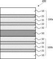
- the barrier film of the present disclosure is The inorganic oxide layer A, the organic coating layer B, the inorganic oxide layer C, and the organic coating layer D are provided in this order on the light-transmitting substrate.
- the refractive indexes of the light-transmitting substrate, the inorganic oxide layer A, the organic coating layer B, the inorganic oxide layer C, and the organic coating layer D are set to n 0 , n A , n B , and n, respectively.
- Examples thereof include a resin film formed of one or more resins selected from polyether ketone, acrylic, polycarbonate, polyurethane, amorphous olefin (Cyclo-Olfin-Polymer: COP) and the like.
- a stretched polyester film particularly a biaxially stretched polyester film, is preferable from the viewpoint of mechanical strength, dimensional stability and heat resistance.
- the polyester film include polyethylene terephthalate film and polyethylene naphthalate film.
- the light-transmitting substrate may be a single layer of a resin film or may have a plurality of resin films. When having a plurality of resin films, each resin film may be directly bonded or may be bonded via an adhesive layer.
- the thickness of each layer constituting the barrier film such as the thickness t 0 of the light transmissive substrate and the thickness of the quantum dot-containing layer are photographed by using, for example, a scanning transmission electron microscope (STEM). It can be calculated from the average value of the values at 20 points by measuring the thickness at 20 points from the image of the cross section.
- STEM scanning transmission electron microscope
- a numerical range For example, in the case of the thickness t 0 of the light transmissive substrate, embodiments in a numerical range such as 5 ⁇ m or more and 200 ⁇ m or less, 5 ⁇ m or more and 25 ⁇ m or less, 8 ⁇ m or more and 50 ⁇ m or less, 10 ⁇ m or more and 50 ⁇ m or less, 10 ⁇ m or more and 25 ⁇ m or less can be mentioned. ..
- the thickness of the first resin film on the side close to the inorganic oxide layer A is preferably 5 ⁇ m or more and 50 ⁇ m or less, and is 8 ⁇ m or more and 25 ⁇ m or less. More preferably, it is more preferably 10 ⁇ m or more and 20 ⁇ m or less.
- the first resin film has the above thickness, the production efficiency of the inorganic oxide layer can be easily improved and the handleability can be easily improved.
- the barrier film of the present disclosure defines the refractive indexes of the inorganic oxide layer A, the organic coating layer B, the inorganic oxide layer C, and the organic coating layer D as n A , n B , n C , and n D , respectively. It is required that n A and n C are larger than n B and n D. Inorganic oxide layers with a high refractive index tend to have good barrier properties. Therefore, by using the inorganic oxide layer A and the inorganic oxide layer C having n A and n C larger than n B and n D , the barrier property of the barrier film is improved and the quantum dots are deteriorated. Can be easily suppressed.
- the inorganic oxide layer A and the inorganic oxide layer C are preferably layers containing aluminum oxide from the viewpoint of sufficient barrier properties, transparency, productivity and the like.
- the content of aluminum oxide in the inorganic oxide layer A and the inorganic oxide layer C is preferably 80% by mass or more, more preferably 90% by mass or more, and 95% by mass or more on a mass basis. It is more preferable to have.
- n A and the refractive index n C are substantially the same.
- n A / n C is preferably 0.98 or more and 1.02 or less, more preferably 0.99 or more and 1.01 or less, and further preferably 1.00. ..
- the lower limit of the thickness t A of the inorganic oxide layer A and the thickness t C of the inorganic oxide layer C are preferably 6 nm or more, and more preferably 7 nm or more, respectively.
- the upper limit of t A and t C is preferably 25 nm or less, more preferably 20 nm or less, more preferably 15 nm or less, still more preferably 12 nm or less, and more preferably 10 nm or less. Is more preferable.
- the water-soluble polymer examples include polyvinyl alcohol, polyvinylpyrrolidone, and an ethylene-vinyl alcohol copolymer.
- polyvinyl alcohol and ethylene-vinyl alcohol copolymer are preferable, and polyvinyl alcohol is more preferable, from the viewpoint of barrier property. That is, the organic coating layer B and the organic coating layer D preferably contain one or more selected from polyvinyl alcohol and an ethylene-vinyl alcohol copolymer, and more preferably contain polyvinyl alcohol.
- metal alkoxide compound examples include metal alkoxide, metal alkoxide hydrolyzate and metal alkoxide polymer.
- the metal alkoxide is a compound represented by the general formula of M (OR) n .
- M represents a metal such as Si, Ti, Al and Zr
- R represents an alkyl group such as a methyl group and an ethyl group.
- Specific examples of the metal alkoxide include tetramethoxysilane, tetraethoxysilane, isopropoxyaluminum and the like.
- t B and t D may have different values, it is preferable that they are substantially the same.
- the fact that t B and t D are substantially the same means that t B / t D is 0.95 or more and 1.05 or less, preferably 0.97 or more and 1.03 or less, and more preferably. It is 0.99 or more and 1.01 or less.
- Most of the light (L1 and L2) incident on the upper barrier film (100a) is composed of the organic coating layer D (32), the inorganic oxide layer C (22), the organic coating layer B (31), and the inorganic oxidation. It passes through the material layer A (21) and the light transmissive substrate (10) and heads toward a member (for example, a brightness improving sheet such as a prism sheet) arranged on the viewer side of the wavelength conversion sheet (200). ..
- the color of the liquid crystal display device to which the wavelength conversion sheet including the barrier film is applied is established by the balance between L1 and L2. Therefore, it is considered that the reason why the color of the liquid crystal display device to which the wavelength conversion sheet is applied changes with time is that the balance between L1 and L2 changes.
- n A and n C are larger than n B and n D. Therefore, the reflection of the interface 2 is a fixed end reflection, the reflection of the interface 3 is a free end reflection, and the reflection of the interface 4 is a fixed end reflection.
- n A and n C are larger than n B and n D , the barrier property is good even if the thickness of the inorganic oxide layer is thin. Therefore, the thickness of the inorganic oxide layer is usually designed to be thin.
- the barrier film of the present disclosure can suppress a change in color due to a high humidity environment by indicating that the value of d 1 in Equation 1 is in the vicinity of an integer of 2 to 13. Even if the value of d 1 is an integer, if it is 0 or 1, it means that the thickness of the organic coating layers B and D is thin. In this case, since the barrier property is not sufficient, the color tone changes due to the deterioration of the quantum dots themselves. When the value of d 1 exceeds the vicinity of 14, it means that the organic coating layers B and D are thick. In this case, the swelling of the organic coating layer becomes excessive and the thickness of the organic coating layer changes significantly, so that the change in color cannot be suppressed. Further, when the value of d 1 exceeds the vicinity of 14, the period of the waveform of the spectral transmittance becomes short, and it becomes difficult to suppress the change in color.
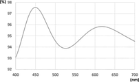
- the waveform of the spectral transmission spectrum of the barrier film has a peak near 450 nm.
- d 1 represented by the formula 1 indicates a value on the plus side of the odd-numbered exact value. Therefore.
- the transmittance at a wavelength of 450 nm decreases when the organic coating layer swells and the waveform of the spectral transmittance of the barrier film shifts to the long wavelength side. That is, in the preferred embodiment 1B, when the organic coating layer swells, the transmittance of L1 decreases.
- D 2 represented by the above formula 2 preferably indicates a range of y ⁇ 0.07 (where y is an integer of 4 to 27), and more preferably indicates a range of y ⁇ 0.05 (where, however). It is even more preferable to indicate the range of y ⁇ 0.03 (where y is an integer of 4 to 27), and even more preferably the range of y ⁇ 0.01 (where y is an integer of 4 to 27). , Y is an integer from 4 to 27). Further, with respect to d 2 represented by the above equation 2, "y" is preferably an integer of 5 to 20, more preferably an integer of 9 to 15, and further preferably an integer of 11 to 13. preferable.
- the reflection at the interface 6 is a reflection that can be ignored as so-called thin film interference. Therefore, the main reflection that should be considered as the reflection that interferes with the reflection of the interface 1-1 (usually the fixed end reflection) is the fixed end reflection of the interface 4. Then, it is necessary to consider the optical distance ( nE ⁇ tE ) of the primer layer as the optical distance of the fixed end reflection of the interface 4.
- the reflection of the interface 4 is the interface 1 when the relationship of the following formula y-1 is satisfied for the light having the wavelength ⁇ . It weakens the reflection of -1 and reduces the reflectance. And, the decrease of the reflectance means that the transmittance increases. Therefore, assuming that the reflections at the interface 1-1 and the interface 4 are both fixed-end reflections, the light having a wavelength ⁇ emitted from the quantum dot-containing layer satisfies the relationship of the following equation y-1. , The transmittance is the highest.
- n B ⁇ t B + n D ⁇ t D the transmittance of the wavelength ⁇ is the highest even when "+ n E x t E " is an odd multiple of " ⁇ / 4”. Then, how many times "n B ⁇ t B + n D ⁇ t D + n E ⁇ t E " is multiplied by " ⁇ / 4" can be calculated by dividing the left side of the equation y-2 by the right side.
- the central wavelength of the primary light of the backlight using quantum dots is approximately 450 nm.
- the reflection at the interface 1-1 is usually a fixed-end reflection.
- the waveform of the spectral transmission spectrum of the barrier film has a peak in the vicinity of 450 nm when d 2 represented by the equation 2 is an odd multiple. Therefore, assuming that the reflection of the interface 1-1 is a fixed-end reflection, the quantum dots are contained by setting d 2 represented by the equation 2 to a value near an odd number, as in the preferred embodiment 2A.
- hydroxyl group-containing compound examples include polyether polyols, polyester polyols, polyester polyurethane polyols, and polyacrylate polyols.
- a polyester polyurethane polyol is particularly preferable from the viewpoint of adhesion to the quantum dot-containing layer and durability.
- the polyester polyurethane polyol can be produced, for example, by the methods described in JP-A-2001-288408 and JP-A-2003-26996.
- the value of the water vapor transmission rate according to JIS K7129-2: 2019 is preferably 0.20 g / m 2 ⁇ day or less, and more preferably 0.15 g / m 2 ⁇ day or less.
- the temperature and humidity conditions for measuring the water vapor transmission rate are 40 ° C. and 90% relative humidity. Further, before measuring the water vapor transmission rate, the sample for measurement shall be exposed to an atmosphere having a temperature of 23 ° C. ⁇ 5 ° C. and a relative humidity of 40% or more and 65% or less for 30 minutes or more.
- the water vapor transmission rate can be measured by, for example, a water vapor transmission rate measuring device (trade name: PERMATRAN) manufactured by MOCON.
- the barrier film preferably has an L * a * b * color system b * value of 1.0 or less, and more preferably ⁇ 1.5 or more and 0.8 or less.
- the b * value is a transparent b * value.
- the light incident surface when measuring the b * value is the surface opposite to the light transmissive substrate.
- the L * a * b * color system is based on the L * a * b * color system standardized by the International Commission on Illumination (CIE) in 1976, and was adopted in JIS Z8781-4: 2013. ing.
- the total thickness of the inorganic oxide layer A, the organic coating layer B, the inorganic oxide layer C and the organic coating layer D is preferably 150 nm or more and 1500 nm or less, more preferably 200 nm or more and 800 nm or less, and 300 nm or more and 650 nm. The following is more preferable.
- the barrier property can be easily improved.
- the total thickness it is possible to suppress that the period of the waveform of the spectral transmittance becomes too short, and it is possible to easily exert the effect by satisfying Equation 1.
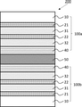
- FIGS. 3 and 4 are cross-sectional views showing an embodiment of the wavelength conversion sheet (200) of the present disclosure.
- the wavelength conversion sheet (200) of FIGS. 3 and 4 has a quantum dot-containing layer (50) containing quantum dots and barrier films (100a, 100b) laminated on both sides of the quantum dot-containing layer. There is. Further, in the wavelength conversion sheet (200) of FIGS. 3 and 4, the surface of the barrier film (100a, 100b) opposite to the light transmissive substrate (10) faces the quantum dot-containing layer (50) side. It is laminated like this.
- Semiconductor crystals such as CdS, CdSe, CdTe, InP, and InGaP are used as the core material of quantum dots from the viewpoints of ease of fabrication, controllability of particle size that can obtain light emission in the visible range, and fluorescence quantum yield. Is preferable.
- the thiol compound may be a monofunctional thiol compound, but a polyfunctional thiol compound is preferable from the viewpoint of improving the strength of the quantum dot-containing layer. Further, among the polyfunctional thiol compounds, a trifunctional thiol compound or a tetrafunctional thiol compound is more preferable.
- the monofunctional thiol compound examples include hexanethiol, 1-heptanethiol, 1-octanethiol, 1-nonanthiol, 1-decanethiol, 3-mercaptopropionic acid, methyl mercaptopropionate, methoxybutyl mercaptopropionate, and the like.
- Examples thereof include octyl mercaptopropionate, tridecyl mercaptopropionate, 2-ethylhexyl-3-mercaptopropionate, n-octyl-3-mercaptopropionate and the like.
- the mass ratio of the ionizing radiation curable compound (or thermosetting resin) to the thiol compound is 80:20 to 35:65. It is preferably 70:30 to 40:60, and more preferably 70:30 to 40:60.
- the thickness of the quantum dot-containing layer is preferably 10 ⁇ m or more and 200 ⁇ m or less, more preferably 20 ⁇ m or more and 150 ⁇ m or less, and further preferably 30 ⁇ m or more and 130 ⁇ m or less.
- "x" in d1 represented by the formula 1 is preferably an odd integer of 3 to 11, and is an odd integer of 9 to 11. Is more preferable. Further, in (i-2A) and (i-4A), "x" in d1 represented by the formula 1 is preferably an even integer of 4 to 12, and is an even integer of 10 to 12. Is more preferable.
- n Z means the refractive index of the quantum dot-containing layer.
- "y” in d2 represented by the formula 2 is preferably an odd integer of 5 to 19, and is an odd integer of 9 to 15. It is more preferable, and it is further preferable that it is an odd integer of 11 to 13. Further, in (ii-2) and (ii-4), "y" in d 2 represented by the formula 2 is preferably an even integer of 6 to 20, and is an even integer of 10 to 16. More preferably, it is even more preferably an even integer of 12-14.
- the amount of light of L2 decreases due to the deterioration of the quantum dots, and the transmittance of L1 also decreases, so that the balance between L1 and L2 is less likely to be lost, and the color It is preferable in that the change in taste can be further suppressed.
- (ii-1A) to (ii-4A) are described from the viewpoint of ensuring that the waveform of the spectral transmission spectrum of the barrier film has a peak in the vicinity of 450 nm.
- (ii-1A) is more preferable from the viewpoint of facilitating the satisfaction of the magnitude relationship of the refractive index.
- "y to y + 0.10" is more preferably y to y + 0.07, more preferably y to y + 0.05, and y to. It is more preferably y + 0.03, and more preferably y to y + 0.01.
- "y-0.10 to y" is more preferably y-0.07 to y, and more preferably y-0.05 to y. Is more preferable, y-0.03 to y is more preferable, and y-0.01 to y is more preferable.
- "y” in d2 represented by the formula 2 is preferably an odd integer of 5 to 19, and is an odd integer of 9 to 15. It is more preferable, and it is further preferable that it is an odd integer of 11 to 13. Further, in (ii-2A) and (ii-4A), "y" in d2 represented by the formula 2 is preferably an even integer of 6 to 20, and is an even integer of 10 to 16. More preferably, it is even more preferably an even integer of 12-14.
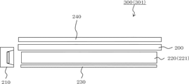
- Examples of the backlight 300 of the present disclosure include an edge light type backlight 301 as shown in FIG. 5 and a direct type backlight 302 as shown in FIG.
- the optical plate 220 used for the direct type backlight 302 of FIG. 6 is an optical member (light diffusing plate 222) having a light diffusing property for making the pattern of the light source 210 difficult to see.
- Examples of the light diffusion plate 222 include a milky white resin plate having a thickness of 1 mm or more and 3 mm or less.
- the light source 210 is a light emitting body that emits primary light, and it is preferable to use a light emitting body that emits primary light having a wavelength corresponding to blue.
- the primary light having a wavelength corresponding to blue preferably has a peak wavelength in the range of 380 nm or more and 480 nm or less.
- the peak wavelength range is more preferably 450 nm ⁇ 7 nm, more preferably 450 nm ⁇ 5 nm, more preferably 450 nm ⁇ 3 nm, and even more preferably 450 nm ⁇ 1 nm.
- the difference in x value ( ⁇ x) and the difference in y value ( ⁇ y) before and after the following high temperature and high humidity test are both with respect to the Yxy color system of the International Commission on Illumination (CIE). It is preferably 0.020 or less, and more preferably 0.010 or less. By setting ⁇ x and ⁇ y to 0.020 or less, the change in color can be suppressed.
- High temperature and high humidity test Test exposed to an atmosphere of 60 ° C and 90% relative humidity for 1000 hours The x and y values after the high temperature and high humidity test are measured immediately after the measurement sample is taken out from the high temperature and high humidity test environment. In addition, the measurement shall be performed in an atmosphere with a temperature of 23 ° C. ⁇ 5 ° C. and a relative humidity of 40% or more and 65% or less.
- Total light transmittance The total light transmittance was measured for the barrier films of Examples and Comparative Examples. The light incident surface was the surface opposite to the light transmissive substrate. A haze meter (HM-150, manufactured by Murakami Color Technology Laboratory) was used as the measuring device. Those with a total light transmittance of 85% or more are acceptable levels. The total light transmittance was measured in an atmosphere having a temperature of 23 ° C. ⁇ 5 ° C. and a relative humidity of 40% or more and 65% or less. In addition, the sample was exposed to the atmosphere for 30 minutes or more before the measurement. The total light transmittance measured in this way means the total light transmittance in the initial stage.
- HM-150 manufactured by Murakami Color Technology Laboratory
- Spectral Transmittance With respect to the barrier films of Example 1 and Comparative Example 1, the spectral transmittance of a wavelength of 380 nm or more and 780 nm or less was measured with the surface opposite to the light transmissive substrate as the light incident surface (measurement wavelength interval; 1 nm). ). A spectrophotometer (trade name: V670) manufactured by JASCO Corporation was used as the measuring device, and the following units were used as accessory units and the like.
- the wavelength conversion sheet in the direct-type backlight was changed to a wavelength conversion sheet of an example and a comparative example in which a high temperature and high humidity test (a test of exposing to an atmosphere of 60 ° C. and a relative humidity of 90% for 1000 hours) was performed.
- a high temperature and high humidity test a test of exposing to an atmosphere of 60 ° C. and a relative humidity of 90% for 1000 hours
- "Direct type backlight for measuring x-value and y-value after high-temperature and high-humidity test” was obtained.
- the work of incorporating the wavelength conversion sheets of the examples and comparative examples in which the high temperature and high humidity test was carried out into the direct backlight was carried out promptly in an atmosphere having a temperature of 23 ° C. ⁇ 5 ° C. and a relative humidity of 40% or more and 65% or less.
- ⁇ X value and y value after high temperature and high humidity test The x value and y value of the Yxy color system of the International Commission on Illumination (CIE) and the x value of the Yxy color system of the International Commission on Illumination (CIE) are turned on from the front direction 500 mm away in a dark room environment by turning on the direct type backlight for measuring the x value and y value after the high temperature and high humidity test. The y value was measured. The measurement atmosphere was a temperature of 23 ° C. ⁇ 5 ° C. and a relative humidity of 40% or more and 65% or less. A spectroradiometer (trade name: SR-3AR) manufactured by Topcon Technohouse Co., Ltd.
- a quantum dot-containing layer coating solution of the following formulation is applied and dried on the surface of one of the two barrier films prepared above on the primer layer side to form a quantum dot-containing layer that has not been irradiated with ionizing radiation.
- a laminated body A was obtained.
- the laminated body A is laminated so that the surface on the quantum dot-containing layer side not irradiated with ionizing radiation and the surface on the primer layer side of the other barrier film face each other, and then irradiated with ultraviolet rays to form the quantum dot-containing layer.
- the curing of the ionizing radiation curable resin composition of Example 1 was allowed to proceed, and the wavelength conversion sheet of Example 1 was obtained.
- the thickness of the quantum dot-containing layer is 100 ⁇ m, and the refractive index is 1.48.
- Comparative Example 5 The inorganic oxide layer A and the inorganic oxide layer C are changed to a thin-film silicon oxide film (refractive index: 1.457), and the thicknesses of the organic coating layer B, the organic coating layer D and the primer layer E are set to the values in Table 2.
- a barrier film and a wavelength conversion sheet of Comparative Example 5 were obtained in the same manner as in Example 1 except for the modification.
Landscapes
- Physics & Mathematics (AREA)
- Nonlinear Science (AREA)
- General Physics & Mathematics (AREA)
- Optics & Photonics (AREA)
- Mathematical Physics (AREA)
- Chemical & Material Sciences (AREA)
- Crystallography & Structural Chemistry (AREA)
- Laminated Bodies (AREA)
- Liquid Crystal (AREA)
- Optical Filters (AREA)
Priority Applications (5)
| Application Number | Priority Date | Filing Date | Title |
|---|---|---|---|
| EP21858163.5A EP4202506B1 (en) | 2020-08-19 | 2021-08-03 | Barrier film, wavelength conversion sheet using same, backlight and liquid crystal display device |
| CN202180008188.2A CN114930203B (zh) | 2020-08-19 | 2021-08-03 | 阻隔膜、及使用其的波长转换片、背光源和液晶显示装置 |
| KR1020227025231A KR102520352B1 (ko) | 2020-08-19 | 2021-08-03 | 배리어 필름, 그리고 이것을 이용한 파장 변환 시트, 백라이트 및 액정 표시 장치 |
| JP2022543357A JP7552703B2 (ja) | 2020-08-19 | 2021-08-03 | バリアフィルム、並びに、これを用いた波長変換シート、バックライト及び液晶表示装置 |
| US17/760,421 US12496802B2 (en) | 2020-08-19 | 2021-08-03 | Barrier film, wavelength conversion sheet using same, backlight and liquid crystal display device |
Applications Claiming Priority (2)
| Application Number | Priority Date | Filing Date | Title |
|---|---|---|---|
| JP2020138751 | 2020-08-19 | ||
| JP2020-138751 | 2020-08-19 |
Publications (2)
| Publication Number | Publication Date |
|---|---|
| WO2022039015A1 true WO2022039015A1 (ja) | 2022-02-24 |
| WO2022039015A8 WO2022039015A8 (ja) | 2022-06-23 |
Family
ID=77364996
Family Applications (1)
| Application Number | Title | Priority Date | Filing Date |
|---|---|---|---|
| PCT/JP2021/028689 Ceased WO2022039015A1 (ja) | 2020-08-19 | 2021-08-03 | バリアフィルム、並びに、これを用いた波長変換シート、バックライト及び液晶表示装置 |
Country Status (7)
| Country | Link |
|---|---|
| US (1) | US12496802B2 (https=) |
| EP (1) | EP4202506B1 (https=) |
| JP (2) | JP6926309B1 (https=) |
| KR (1) | KR102520352B1 (https=) |
| CN (1) | CN114930203B (https=) |
| TW (1) | TWI876082B (https=) |
| WO (1) | WO2022039015A1 (https=) |
Cited By (2)
| Publication number | Priority date | Publication date | Assignee | Title |
|---|---|---|---|---|
| WO2022196756A1 (ja) * | 2021-03-18 | 2022-09-22 | 大日本印刷株式会社 | 波長変換シート用フィルム、並びに、これを用いた波長変換シート、バックライト及び液晶表示装置 |
| WO2025084339A1 (ja) * | 2023-10-20 | 2025-04-24 | 大日本印刷株式会社 | 波長変換シートの製造方法 |
Families Citing this family (5)
| Publication number | Priority date | Publication date | Assignee | Title |
|---|---|---|---|---|
| JP6926309B1 (ja) * | 2020-08-19 | 2021-08-25 | 大日本印刷株式会社 | バリアフィルム、並びに、これを用いた波長変換シート、バックライト及び液晶表示装置 |
| EP4071809A1 (en) * | 2021-04-07 | 2022-10-12 | Samsung Electronics Co., Ltd. | Color conversion structure, display apparatus, and method of manufacturing the display apparatus |
| JP7572479B2 (ja) * | 2021-11-11 | 2024-10-23 | 株式会社ツジデン | 直下型点光源バックライトユニット、及び該直下型点光源バックライトユニットを搭載した液晶装置。 |
| JP2023096728A (ja) * | 2021-12-27 | 2023-07-07 | 日鉄ケミカル&マテリアル株式会社 | 感光性樹脂組成物、硬化膜、硬化膜付き基板およびその製造方法、ならびに表示装置 |
| US12211457B1 (en) | 2023-09-26 | 2025-01-28 | Apple Inc. | Dynamic quantum dot color shift compensation systems and methods |
Citations (8)
| Publication number | Priority date | Publication date | Assignee | Title |
|---|---|---|---|---|
| JP2001288408A (ja) | 2000-04-07 | 2001-10-16 | The Inctec Inc | 蒸着コーティング液 |
| JP2003026996A (ja) | 2001-07-18 | 2003-01-29 | The Inctec Inc | 蒸着塗布液 |
| JP2007073219A (ja) * | 2005-09-05 | 2007-03-22 | Seiko Epson Corp | 有機エレクトロルミネッセンス装置、有機エレクトロルミネッセンス装置の製造方法、及び電子機器 |
| KR101421973B1 (ko) * | 2013-08-20 | 2014-07-23 | (주)아이컴포넌트 | 디스플레이용 광학 투명 복합 필름 및 이의 제조방법 |
| JP2016213369A (ja) * | 2015-05-12 | 2016-12-15 | 凸版印刷株式会社 | 波長変換シート用保護フィルム、波長変換シート及びバックライトユニット |
| JP2017094557A (ja) * | 2015-11-20 | 2017-06-01 | 凸版印刷株式会社 | ガスバリア性積層フィルム及び波長変換シート |
| JP2019171661A (ja) * | 2018-03-28 | 2019-10-10 | 凸版印刷株式会社 | ガスバリア性積層フィルム,波長変換シート |
| JP2020019141A (ja) * | 2018-07-30 | 2020-02-06 | 凸版印刷株式会社 | バリアフィルム、波長変換シート、及び、波長変換シートの製造方法 |
Family Cites Families (18)
| Publication number | Priority date | Publication date | Assignee | Title |
|---|---|---|---|---|
| JP5595190B2 (ja) * | 2010-08-31 | 2014-09-24 | 富士フイルム株式会社 | 機能性フィルムおよび機能性フィルムの製造方法 |
| WO2012132239A1 (ja) | 2011-03-31 | 2012-10-04 | パナソニック株式会社 | 蛍光フィルムおよび表示フィルム |
| JP6094406B2 (ja) | 2013-07-11 | 2017-03-15 | Jsr株式会社 | 感放射線性樹脂組成物、硬化膜、発光素子、波長変換フィルムおよび発光層の形成方法 |
| KR101532246B1 (ko) | 2013-08-09 | 2015-06-29 | 주식회사 성우하이텍 | 리벳 너트 유닛 |
| JP6087872B2 (ja) * | 2013-08-12 | 2017-03-01 | 富士フイルム株式会社 | 光学フィルム、バリアフィルム、光変換部材、バックライトユニットおよび液晶表示装置 |
| EP3064829B1 (en) * | 2013-09-13 | 2018-07-25 | Toppan Printing Co., Ltd. | Wavelength conversion sheet and backlight unit |
| EP3171072A4 (en) | 2014-07-18 | 2018-04-04 | Toppan Printing Co., Ltd. | Protective film for wavelength conversion sheet, wavelength conversion sheet and backlight unit |
| JP6589463B2 (ja) | 2015-08-27 | 2019-10-16 | 大日本印刷株式会社 | 量子ドット用バリアフィルムの選択方法、量子ドット用バリアフィルム、量子ドットシート、バックライト及び液晶表示装置 |
| JP6720985B2 (ja) * | 2015-12-17 | 2020-07-08 | コニカミノルタ株式会社 | ガスバリアーフィルム |
| JPWO2017126609A1 (ja) * | 2016-01-20 | 2018-11-15 | 凸版印刷株式会社 | 発光体保護フィルム及びその製造方法、並びに波長変換シート及び発光ユニット |
| WO2017169977A1 (ja) | 2016-03-31 | 2017-10-05 | 凸版印刷株式会社 | バリアフィルム及びその製造方法、波長変換シート及びその製造方法、並びに、光学積層体及びその製造方法 |
| JP6759667B2 (ja) | 2016-03-31 | 2020-09-23 | 凸版印刷株式会社 | 光学積層体及びその製造方法、並びに、波長変換シート及びその製造方法 |
| WO2017179513A1 (ja) * | 2016-04-11 | 2017-10-19 | 凸版印刷株式会社 | バリアフィルム積層体及びその製造方法、波長変換シート、バックライトユニット、並びにエレクトロルミネッセンス発光ユニット |
| JP6769307B2 (ja) | 2017-01-05 | 2020-10-14 | 凸版印刷株式会社 | 光学積層体及び波長変換シート |
| CN110945599B (zh) | 2017-06-07 | 2023-10-10 | 华盛顿大学 | 等离子体约束系统及使用方法 |
| WO2019085851A1 (zh) | 2017-11-01 | 2019-05-09 | 苏州东微半导体有限公司 | 沟槽型功率晶体管 |
| JP7031325B2 (ja) | 2018-01-22 | 2022-03-08 | 大日本印刷株式会社 | バリアフィルム、及びバリアフィルムを用いた波長変換シート |
| JP6926309B1 (ja) * | 2020-08-19 | 2021-08-25 | 大日本印刷株式会社 | バリアフィルム、並びに、これを用いた波長変換シート、バックライト及び液晶表示装置 |
-
2020
- 2020-12-22 JP JP2020212727A patent/JP6926309B1/ja active Active
-
2021
- 2021-08-03 CN CN202180008188.2A patent/CN114930203B/zh active Active
- 2021-08-03 EP EP21858163.5A patent/EP4202506B1/en active Active
- 2021-08-03 KR KR1020227025231A patent/KR102520352B1/ko active Active
- 2021-08-03 TW TW110128548A patent/TWI876082B/zh active
- 2021-08-03 WO PCT/JP2021/028689 patent/WO2022039015A1/ja not_active Ceased
- 2021-08-03 JP JP2022543357A patent/JP7552703B2/ja active Active
- 2021-08-03 US US17/760,421 patent/US12496802B2/en active Active
Patent Citations (8)
| Publication number | Priority date | Publication date | Assignee | Title |
|---|---|---|---|---|
| JP2001288408A (ja) | 2000-04-07 | 2001-10-16 | The Inctec Inc | 蒸着コーティング液 |
| JP2003026996A (ja) | 2001-07-18 | 2003-01-29 | The Inctec Inc | 蒸着塗布液 |
| JP2007073219A (ja) * | 2005-09-05 | 2007-03-22 | Seiko Epson Corp | 有機エレクトロルミネッセンス装置、有機エレクトロルミネッセンス装置の製造方法、及び電子機器 |
| KR101421973B1 (ko) * | 2013-08-20 | 2014-07-23 | (주)아이컴포넌트 | 디스플레이용 광학 투명 복합 필름 및 이의 제조방법 |
| JP2016213369A (ja) * | 2015-05-12 | 2016-12-15 | 凸版印刷株式会社 | 波長変換シート用保護フィルム、波長変換シート及びバックライトユニット |
| JP2017094557A (ja) * | 2015-11-20 | 2017-06-01 | 凸版印刷株式会社 | ガスバリア性積層フィルム及び波長変換シート |
| JP2019171661A (ja) * | 2018-03-28 | 2019-10-10 | 凸版印刷株式会社 | ガスバリア性積層フィルム,波長変換シート |
| JP2020019141A (ja) * | 2018-07-30 | 2020-02-06 | 凸版印刷株式会社 | バリアフィルム、波長変換シート、及び、波長変換シートの製造方法 |
Non-Patent Citations (1)
| Title |
|---|
| See also references of EP4202506A4 |
Cited By (3)
| Publication number | Priority date | Publication date | Assignee | Title |
|---|---|---|---|---|
| WO2022196756A1 (ja) * | 2021-03-18 | 2022-09-22 | 大日本印刷株式会社 | 波長変換シート用フィルム、並びに、これを用いた波長変換シート、バックライト及び液晶表示装置 |
| US12025882B2 (en) | 2021-03-18 | 2024-07-02 | Dai Nippon Printing Co., Ltd. | Film for wavelength conversion sheet, and wavelength conversion sheet, backlight, and liquid crystal display device which use same |
| WO2025084339A1 (ja) * | 2023-10-20 | 2025-04-24 | 大日本印刷株式会社 | 波長変換シートの製造方法 |
Also Published As
| Publication number | Publication date |
|---|---|
| CN114930203A (zh) | 2022-08-19 |
| EP4202506B1 (en) | 2025-11-26 |
| US20230104432A1 (en) | 2023-04-06 |
| US12496802B2 (en) | 2025-12-16 |
| TWI876082B (zh) | 2025-03-11 |
| EP4202506C0 (en) | 2025-11-26 |
| EP4202506A1 (en) | 2023-06-28 |
| KR102520352B1 (ko) | 2023-04-10 |
| TW202233429A (zh) | 2022-09-01 |
| EP4202506A4 (en) | 2024-08-14 |
| JP2022035938A (ja) | 2022-03-04 |
| JPWO2022039015A1 (https=) | 2022-02-24 |
| JP7552703B2 (ja) | 2024-09-18 |
| JP6926309B1 (ja) | 2021-08-25 |
| WO2022039015A8 (ja) | 2022-06-23 |
| KR20220107318A (ko) | 2022-08-02 |
| CN114930203B (zh) | 2023-04-28 |
Similar Documents
| Publication | Publication Date | Title |
|---|---|---|
| JP6926309B1 (ja) | バリアフィルム、並びに、これを用いた波長変換シート、バックライト及び液晶表示装置 | |
| JP7025585B1 (ja) | 波長変換シート用のバリアフィルム、並びに、これを用いた波長変換シート、バックライト及び液晶表示装置 | |
| JP7036185B2 (ja) | バリアフィルム、並びに、これを用いた波長変換シート、バックライト及び液晶表示装置 | |
| JP7694238B2 (ja) | バリアフィルム、並びに、これを用いた波長変換シート、バックライト及び液晶表示装置 | |
| US12025882B2 (en) | Film for wavelength conversion sheet, and wavelength conversion sheet, backlight, and liquid crystal display device which use same | |
| US12078890B2 (en) | Barrier film, and wavelength conversion sheet, back light, and liquid crystal display device which use same | |
| US12019332B2 (en) | Barrier film, and wavelength conversion sheet, backlight, and liquid crystal display device in which same is used, as well as method for selecting barrier film | |
| JP7120287B2 (ja) | バリアフィルム、並びに、これを用いた波長変換シート、バックライト及び液晶表示装置、並びに、バリアフィルムの選定方法 | |
| WO2024043127A1 (ja) | 波長変換シート、並びに、これを用いたバックライト及び液晶表示装置 |
Legal Events
| Date | Code | Title | Description |
|---|---|---|---|
| 121 | Ep: the epo has been informed by wipo that ep was designated in this application |
Ref document number: 21858163 Country of ref document: EP Kind code of ref document: A1 |
|
| ENP | Entry into the national phase |
Ref document number: 2022543357 Country of ref document: JP Kind code of ref document: A |
|
| ENP | Entry into the national phase |
Ref document number: 20227025231 Country of ref document: KR Kind code of ref document: A |
|
| NENP | Non-entry into the national phase |
Ref country code: DE |
|
| ENP | Entry into the national phase |
Ref document number: 2021858163 Country of ref document: EP Effective date: 20230320 |
|
| WWG | Wipo information: grant in national office |
Ref document number: 2021858163 Country of ref document: EP |
|
| WWG | Wipo information: grant in national office |
Ref document number: 17760421 Country of ref document: US |