WO2022024610A1 - 電流センサ - Google Patents
電流センサ Download PDFInfo
- Publication number
- WO2022024610A1 WO2022024610A1 PCT/JP2021/023978 JP2021023978W WO2022024610A1 WO 2022024610 A1 WO2022024610 A1 WO 2022024610A1 JP 2021023978 W JP2021023978 W JP 2021023978W WO 2022024610 A1 WO2022024610 A1 WO 2022024610A1
- Authority
- WO
- WIPO (PCT)
- Prior art keywords
- shield
- facing surface
- current
- sensor
- magnetic
- Prior art date
- Legal status (The legal status is an assumption and is not a legal conclusion. Google has not performed a legal analysis and makes no representation as to the accuracy of the status listed.)
- Ceased
Links
Images




Classifications
-
- G—PHYSICS
- G01—MEASURING; TESTING
- G01R—MEASURING ELECTRIC VARIABLES; MEASURING MAGNETIC VARIABLES
- G01R15/00—Details of measuring arrangements of the types provided for in groups G01R17/00 - G01R29/00, G01R33/00 - G01R33/26 or G01R35/00
- G01R15/14—Adaptations providing voltage or current isolation, e.g. for high-voltage or high-current networks
- G01R15/20—Adaptations providing voltage or current isolation, e.g. for high-voltage or high-current networks using galvano-magnetic devices, e.g. Hall-effect devices, i.e. measuring a magnetic field via the interaction between a current and a magnetic field, e.g. magneto resistive or Hall effect devices
- G01R15/207—Constructional details independent of the type of device used
-
- G—PHYSICS
- G01—MEASURING; TESTING
- G01R—MEASURING ELECTRIC VARIABLES; MEASURING MAGNETIC VARIABLES
- G01R1/00—Details of instruments or arrangements of the types included in groups G01R5/00 - G01R13/00 and G01R31/00
- G01R1/02—General constructional details
- G01R1/18—Screening arrangements against electric or magnetic fields, e.g. against earth's field
Definitions
- the present invention relates to a current sensor that detects a measured current based on a magnetic field generated by a measured current flowing in a current path.
- the current path through which the current to be measured flows is bent in a U shape, and both ends of the current path abut on both opposite long sides of the rectangular insulating substrate.
- one side surface of each end of the current path is arranged so as to be located near one short side of the insulating substrate.
- the magnetic field control plate that controls the magnetic field generated by the measured current is bent in a U shape, and one end of the magnetic field control plate is located on the side surface of the current path among the short sides of the insulating substrate.
- the magnetic sensor element for measuring the magnetic field is arranged at the center of the opening width of the magnetic field control plate so as to be in contact with the short side. With the magnetic field control plate, the magnetic field due to the current path can be concentrated around the magnetic sensor element, and the external magnetic field can be weakened to magnetically shield the magnetic sensor element.
- the magnetic field generated by the measured current is amplified by the magnetic field control plate while suppressing the influence of the external magnetic field by the magnetic field control plate as a shield member, so that the opening width of the magnetic field control plate is widened.
- the magnetic field can be reliably detected by the magnetic sensor element arranged in the center.
- the magnetic field control plate has the effect of amplifying the magnetic field, it tends to reach magnetic saturation, so that it cannot detect current and does not function as a current sensor.
- the present invention can sufficiently attenuate the external magnetic field and suppress or control the magnetic saturation, thereby expanding the current measurement range, for example, in the current measurement range such as the measured current. It is an object of the present invention to provide a current sensor provided with a shield member capable of expanding and widening a measurable frequency.
- the current sensor of the present invention has a first shield and a second shield, which are arranged apart from each other with a magnetic sensor capable of detecting a magnetic field generated by a current to be measured flowing in a current path.
- a current sensor including a shield and a shield member provided with a third shield, wherein the first shield is a magnetic sensor that sandwiches a current path in a first direction in which the magnetic sensor and the current path face each other.
- the second shield has a second facing surface along the first direction
- the third shield has a first facing surface facing the current path and is arranged on the opposite side of the current path.
- the second shield and the third shield have a third facing surface, and the second facing surface and the third facing surface are arranged so as to face each other with the magnetic sensor and the current path interposed therebetween. It is a feature. In this way, by forming the shield surrounding the bus bar through which the measured current flows with a plurality of discontinuous members, it becomes possible to suppress or control the magnetic saturation in the shield while suppressing the influence of the external magnetic field. The range of current measurement can be expanded.
- the ends of the second shield and the third shield on the first shield side are located closer to the magnetic sensor than the first facing surface of the first shield.
- the influence of the external magnetic field can be effectively suppressed.
- current sensors having the same configuration are lined up in the second direction in which the second facing surface and the third facing surface face each other, the magnetic field generated by the current flowing through the adjacent bus bar can be effectively blocked. , It is possible to suppress the influence of the magnetic field on the magnetic sensor.
- the ends of the first shield on the second shield side and the third shield side are the second facing surface and the second facing surface. It is preferable that the sensor is arranged at a position farther from the magnetic sensor than the third facing surface. As a result, the influence of the external magnetic field can be effectively suppressed. In particular, the influence of the external magnetic field along the first direction in which the magnetic sensor and the current path face each other can be reliably suppressed by the first shield.
- the current path extends along the third direction orthogonal to the first direction and the second direction, and when viewed along the first direction, the second direction in the third direction. It is preferable that both ends of the shield and the third shield are located outside the first shield. As a result, at the time of insert molding, the support of the first shield and the support of the second shield and the third shield can be independently performed, so that the assembling property can be improved.
- the first shield, the second shield, and the third shield are each divided.
- the shield can be divided into a form suitable for suppressing the influence of various external magnetic fields, so that the influence of the external magnetic field can be effectively suppressed and the current measurement range can be adjusted.
- a current sensor capable of expanding the current measurement range by sufficiently attenuating an external magnetic field and suppressing or controlling magnetic saturation.
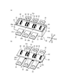
- FIG. 1 is a perspective view showing the configuration of the current sensor according to the first embodiment of the present invention
- FIG. 2 is a perspective view showing the configuration of the current sensor according to the first embodiment of the present invention
- FIG. 2 is a perspective view showing the configuration of the current sensor according to the first embodiment of the present invention
- FIG. 2 is a perspective view showing the configuration of the current sensor according to the first embodiment of the present invention
- FIG. 2 is a perspective view of the current sensor shown in (a) without showing the base member.
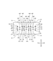
- the front view shown in (b) is a plan view in which the illustration of the bus bar is omitted in (a).
- (A) is a perspective view of the base member viewed from above, and (b) is a perspective view of the base member viewed from below. It is a top view which shows the arrangement of the base member, the 2nd shield and the 3rd shield, and a magnetic sensor. It is a bottom view which shows the position of the 1st shield with respect to the base member in which the 2nd shield and the 3rd shield are arranged virtually.
- (A) shows an enlarged arrangement of the bus bar, the corresponding magnetic sensor, and the first shield, the second shield, and the third shield provided so as to surround them in the second embodiment.
- the front view, (b) is an enlargement of the arrangement of the bus bar, the corresponding magnetic sensor, and the first shield, the second shield, and the third shield provided so as to surround them in the third embodiment. It is a front view shown by. It is a front view which enlargedly shows the arrangement of the 1st shield, the 2nd shield, and the 3rd shield provided around the bus bar and the magnetic sensor corresponding thereto in 4th Embodiment.
- XYZ coordinates are shown as reference coordinates.
- the Z1-Z2 direction is referred to as a vertical direction (first direction)
- the X1-X2 direction is referred to as a front-back direction (third direction)
- the Y1-Y2 direction is referred to as a left-right direction (second direction).
- the X1-X2 direction and the Y1-Y2 direction are perpendicular to each other, and the XY plane including them is perpendicular to the Z1-Z2 direction.
- a state in which the lower side (Z2 side) is viewed from the upper side (Z1 side) may be referred to as a plan view.
- the current sensor 10 includes a base member 11, a substrate 20, three magnetic sensors 21, 22, 23, and 3 as a current path.
- the base member 11 is made of non-magnetic materials, three bus bars 31, 32, 33, three first shields 41, 51, 61, three second shields 42, 52, 62, and three third shields. It is insert-molded together with 43, 53, 63.
- the base member 11 has a rectangular outer shape extending in the left-right direction (Y1-Y2 direction) in a plan view from the upper side (Z1 side) to the lower side (Z2 side). As shown in FIG. 4A, this external shape is formed by four outer wall portions 12 corresponding to the four sides of a rectangle, and is recessed downward inside the four outer wall portions 12 in a plan view.
- a base 13 is provided. As a result, the upper surface 13a of the base portion 13 is located below the upper surface of the outer wall portion 12. On the other hand, as shown in FIG. 4B, the bottom surface 13b of the base portion 13 forms a flat surface integrated with the outer wall portion 12.
- the substrate 20 extends along the left-right direction (Y1-Y2 direction) and is inside the four outer wall portions 12 of the base member 11. It is a rectangular plate material in a plan view, which is arranged above the base 13.
- the first insertion hole 20a, the second insertion hole 20b, the third insertion hole 20c, and the fourth insertion hole 20d are respectively in the thickness direction (vertical direction, Z1-Z2). It is formed so as to penetrate in the direction).
- the first insertion hole 20a is arranged so that the leftmost second shield 42 can be inserted vertically, and the second insertion hole 20b is a third shield 43 facing the second shield 42 and a second shield. It is arranged so that it can be inserted in a state where it is separated from the 52, and the third insertion hole 20c can be inserted in a state where the third shield 53 facing the second shield 52 and the second shield 62 are separated from each other.
- the fourth insertion hole 20d is arranged so that the third shield 63 on the far right side can be inserted.
- the first magnetic sensor 21 on the left side has a pair of shields 42, 43 (second shields 42, third) facing each other in the left-right direction. It is arranged at an intermediate position between the shields 43) and above the first shield 41 and the first bus bar 31 located above the first shield 41 in the vertical direction.
- the second magnetic sensor 22 is arranged at an intermediate position between a pair of shields 52 and 53 (second shield 52 and third shield 53) facing each other in the left-right direction. , In the vertical direction, it is arranged above the first shield 51 and the second bus bar 32 located above the first shield 51. Further, the third magnetic sensor 23 is also arranged at an intermediate position between the pair of shields 62 and 63 (second shield 62 and third shield 63) facing each other in the left-right direction, similarly to the first magnetic sensor 21. And, in the vertical direction, it is arranged above the first shield 61 and the third bus bar 33 located above the first shield 61.
- the three bus bars 31, 32, and 33 as current paths extend in the front-rear direction (X1-X2 direction) and have a long plate shape having the same shape as each other, so that the upper and lower surfaces are orthogonal to each other in the vertical direction. Be placed. As shown in FIG. 2A, the upper surfaces of the three bus bars 31, 32, and 33 face the three magnetic sensors 21, 22, and 23, respectively, and the lower surfaces of the three bus bars 41, respectively, face the three first shields 41. , 51 and 61, respectively. More specifically, in the vertical direction, the first bus bar 31 on the left side is arranged so as to face each other between the magnetic sensor 21 on the left side and the first shield 41 on the left side, and the second bus bar 32 in the center in the left-right direction.
- the third bus bar 33 on the right side is the third magnetic sensor 23 on the right side and the first on the right side. They are arranged so as to face each other between the shields 61.
- the first bus bar 31 on the left side has a rectangular central portion 31a in the center in the longitudinal direction (front-rear direction, X1-X2 direction) and both ends on the outer side in the longitudinal direction of the central portion 31a. It includes two intermediate portions 31b provided so as to extend each, and two outer portions 31c provided so as to extend from both ends on the outer sides in the longitudinal direction of the two intermediate portions 31b.
- the first bus bar 31 has a symmetrical shape in the width direction (horizontal direction, Y1-Y2 direction), the intermediate portion 31b is wider than the central portion 31a, and the outer portion 31c is wider than the intermediate portion 31b. Has a large shape.
- the planar shape of the first bus bar 31 is the same for the second bus bar 32 and the third bus bar 33.
- the first, second, and third shields will be described by taking as an example the first shield 41 on the left side and the corresponding set of the second shield 42 and the third shield 43.
- the set of the first shield 51, the second shield 52, and the third shield 53 in the center in the left-right direction, and the set of the first shield 61, the second shield 62, and the third shield 63 on the right side have the same configuration. be.
- the number of sets of the first, second, and third shields, and the corresponding combinations of the bus bar and the magnetic sensor is not limited to three as shown in FIG. For example, it may be one, two, or four or more.
- the first shield 41, the second shield 42, and the third shield 43 have a configuration in which five magnetic shield plates made of the same magnetic material are laminated. Have. These shields 41, 42, 43 are preferably formed of a soft magnetic material, for example, an electromagnetic steel plate or permalloy. The second shield 42 and the third shield 43 have the same shape as each other.
- the first shield 41 is arranged so as to extend along the left-right direction (Y1-Y2 direction), and the first facing surface 41a, which is the upper surface thereof, faces the lower surface of the first bus bar 31. As shown in FIG. 2B, of the first bus bar 31, the first shield 41 faces the central portion 31a.
- the second shield 42 and the third shield 43 are arranged at the same height position in the vertical direction so as to face each other in the left-right direction (Y1-Y2 direction). As a result, the second facing surface 42a of the second shield 42 and the third facing surface 43a of the third shield 43 face each other.
- both end faces 41b and 41c of the first shield 41 are more than the outer surface 42b of the second shield 42 and the outer surface 43b of the third shield 43, respectively. It is located on the outside. Specifically, the left end surface 41b (the end portion on the second shield 42 side) of the first shield 41 is located on the left side by a distance D11 with respect to the second facing surface 42a of the second shield 42, and is on the right side. The end surface 41c (the end on the third shield 43 side) is located to the right of the third facing surface 43a of the third shield 43 by a distance D11.
- the end portion (second end surface 41c) on the third shield 43 side is arranged at a position farther from the magnetic sensor 21 than the second facing surface 42a and the third facing surface 43a, respectively.
- the lower surface 42c of the second shield 42 and the lower surface 43c of the third shield 43 are separated from the first facing surface 41a of the first shield 41 by a distance D12.
- the ends of the second shield 42 and the third shield 43 on the first shield 41 side (lower side) are more magnetic than the first facing surface 41a of the first shield 41. It is located on the sensor 21 side.
- the distance D12 applies an external magnetic field to the magnetic sensor 21 surrounded by the first shield 41, the second shield 42, and the third shield 43, depending on the specifications of the current sensor 10 and the usage environment. It is set so that it can be shielded to a predetermined range and it is difficult to reach magnetic saturation.
- the second shield 42 and the third shield 43 are arranged at a distance D12 with respect to the first shield 41, the surroundings including the magnetic field generated by the measured current flowing through the adjacent second bus bar 32. It is possible to suppress the influence of the external magnetic field existing in.
- both end faces 42d and 42e of the second shield 42 are outside the both end faces 41d and 41e of the first shield 41 by a distance D13, respectively. positioned.
- both end faces 43d and 43e of the third shield 43 are located outside the both end faces 41d and 41e of the first shield 41 by a distance D13, respectively.
- both ends of the second shield 42 both end faces 42d, 42e
- Both ends 43d, 43e) are located on the outside of the first shield 41, respectively.
- the first shield 41 and the second shield 41 and the second shield 41 are arranged at the time of insert molding. Since the shield 42 and the third shield 43 can be individually pressed, it is possible to easily manufacture the shield 42 with high position accuracy.
- Base member 11 three bus bars 31, 32, 33, three first shields 41, 51, 61, three second shields 42, 52, 62, and three third shields 43, 53, 63. And are manufactured by insert molding.
- the base 13 of the base member 11 is formed with bottomed upper holding holes h11 to h16, h21 to h24, and h31 to h34 from the upper surface 13a to the lower side.
- the bottomed lower holding holes h41 to h52, h61 to h66, and h71 to 76 are recessed from the bottom surface 13b to the upper side.
- pins are pinned to the first shield 41, the second shield 42, and the third shield 43. It is grasped by pressing. After the insert molding, the pin is removed so that the upper and lower holding holes h11 to h16, h21 to h24, h31 to h34, h41 to h52, h61 to h66, and h71 to 76 are pressed against the pin. Is recessed.
- the first upper holding holes h11, h12, h13, h14, h15, and h16 are formed in order from the left side to the right side in the center in the front-rear direction.
- Second upper holding holes h21, h22, h23, and h24 are formed in this order from the left side to the right side at positions behind the first upper holding holes h11 to h16.
- the third upper holding hole h31 , H32, h33, h34 are formed.
- the first lower holding holes h41, h42 / h43, h44, h45, h46 / h47, h48, h49, h50, h51, and h52 are formed.
- the three pairs of holding holes h42 / h43, h46 / h47, and h50 / h51 are arranged symmetrically in the front-rear direction, respectively.
- the second lower holding holes h61, h62 at positions in front of the holding holes h41, h44, h45, h48, h49, and h52, the second lower holding holes h61, h62, in order from the left side to the right side, h63, h64, h65, and h66 are formed, and in the rear position, a third position corresponding to each of the second lower holding holes h61 to h66 in the front-rear direction, in order from the left side to the right side.
- Lower holding holes h71, h72, h73, h74, h75, and h76 are formed.
- the second shield 42 and the third shield 43 are positioned in the XY plane direction at the positions where the upper holding holes h11 to h16, h21 to h24, and h31 to h34 are formed after the molding is completed.
- Pins (not shown) for this purpose are arranged, and the pins are removed after the molding is completed (see FIG. 5).
- the traces from which the pins have been removed are the above-mentioned various holding holes.
- the left side surface is located at a position where the rear holding hole h21 is located and the front upper holding hole h31 is located. It is regulated by the arranged pin, and the right side surface (second facing surface 42a) is regulated by the pin arranged at the position where the holding hole h11 in the center in the front-rear direction is located.
- the first lower holding hole h41, h42 / h43, h44, h45, h46 / h47, h48, h49, h50 / h51, h52 is formed at the position where the first lower holding hole h41, h42 / h43, h44, h45, h46 / h47, h48, h49, h50 / h51, h52 is formed.
- Pins for positioning the shields 41, 51, and 61 in the vertical direction are arranged, and the pins are removed after the molding is completed (see FIG. 6).
- the traces from which the pins have been removed are the above-mentioned various holding holes.
- the first shield 41 on the left side is positioned by a pin arranged at a position shown in FIG. 6 where four first lower holding holes h41, h42, h43, and h44 located on the left side are located.
- the second lower holding holes h61 to h66 are located in front of the first shields 41, 51 and 61, and the third lower holding holes h71 to h76 are the first shields 41, 51 and 61. It is in a position behind.
- these lower holding holes h61 to h66 and h71 to h76 pins for positioning the second shield 42 and the third shield 43 in the vertical direction are arranged, and the pins are removed after the molding is completed.
- the leftmost second shield 42 is positioned in the vertical direction by pins arranged in the second lower holding hole h61 and the corresponding third lower holding hole h71 in the front-rear direction. Be done.
- the positioning pins are removed, and the upper holding holes h11 to h16, h21 to h24, h31 to h34 and the lower holding holes h41 to h52, h61 to h66 are located at the positions where the pins are removed. h71 to 76 are formed.
- the substrate 20 is arranged on the base 13.
- the leftmost second shield 42 is located in the first insertion hole 20a, and the third shield 43 and the second shield 52 on the right side thereof are parallel to each other in the second insertion hole 20b.
- the third shield 53 and the second shield 62 on the right side thereof are positioned so as to be parallel to each other in the third insertion hole 20c, and the third on the far right side in the fourth insertion hole 20d. It is arranged so that the shield 63 is located.
- three magnetic sensors 21, 22, and 23 are arranged in advance on the lower surface before being arranged on the base 13.
- the magnetic sensor 21 and the first bus bar 31 facing each other up and down are sandwiched by the second shield 42 and the third shield 43 in the left-right direction, and surrounded by the first shield 41 below.
- the first facing surface 41a of the first shield 41 is separated from the second shield 42 and the third shield 43 by a distance D12.
- a magnetic field is generated when a measured current flows through the first bus bar 31 as a current path, and the three shields 41, 42, and 43 surrounding the first bus bar 31 from three directions are yokes against this magnetic field. Functions as.
- the concentration of the magnetic force is controlled by the magnitude of the distance D12, and the three shields 41, 42, and 43 are magnetically saturated. It prevents it from reaching.
- the current measurement range for example, it is possible to expand the current measurement range such as the measured current and widen the measurable frequency band.
- the configurations of Example 1 and Comparative Example are as follows.
- the first shield 41 is made of a soft magnetic material such as an electromagnetic steel plate and permalloy, and has a five-sheet laminated structure with a total thickness of 1.5 mm (Z1-Z2 direction), a width of 13 mm (Y1-Y2 direction), and a length of 6 mm (X1). It has a shape (-X2 direction).
- the second shield 42 is made of an electromagnetic steel plate and a soft magnetic material such as permalloy), and has a five-sheet laminated structure with a total thickness of 1.5 mm (Y1-Y2 direction), a height of 9.5 mm (Z1-Z2 direction), and a length. It has a shape of 8 mm (X1-X2 direction).
- the third shield 43 is made of the same material and shape as the second shield 42.
- the distance D11 is 2 mm
- the distance D12 is 0.5 mm
- the distance D13 is 1 mm.
- the first bus bar 31 is arranged 1.5 mm above the first facing surface 41a of the first shield 41, and the magnetic sensor 21 is arranged further above.
- the shield in the comparative example has a continuous U-shape with the upper side open when viewed from the front, and is not divided like the first, second, and third shields of the first embodiment.
- the material and length (X1-X2 direction) of the shield are the same as in the first embodiment, and the thickness and width (or height) of the portions corresponding to the first, second, and third shields of the first embodiment are the same as those in the first embodiment. It is the same as the corresponding shield in Example 1.
- the shapes of the magnetic sensor and the bus bar, and the positions of the shield member with respect to the inner surface (opposing surface) are the same as those in the first embodiment.
- the maximum magnetic flux density was 1.6 T and the influence from the adjacent bus bar was 0.1%, whereas in the first embodiment, the influence was 0.1%.
- the maximum magnetic flux density was 0.4 T, and the influence from the adjacent bus bar was 0.7%.
- the adjacent effect was 0.1% in Comparative Example, whereas it was 0.7% in Example 1, which is slightly larger than that of Comparative Example.
- this is caused by the fact that a gap is created due to the division of the shield, which makes it somewhat susceptible to the influence of adjacency, and is acceptable in actual products. That is, the degree of influence does not have a great influence on the measurement accuracy of the current sensor 10, and is within an acceptable range when the suppression of magnetic saturation is prioritized.
- Example 1 the current required to reach magnetic saturation in Example 1 was about twice that of Comparative Example.
- the measurement range of the current can be expanded, and the influence of the external magnetic field such as the magnetic field generated by the current flowing through the adjacent bus bar is sufficiently suppressed. It was found that the magnetic field generated by the flow of the measured current through 31 can be amplified by the first shield 41, the second shield 42, and the third shield 43, which function as yokes.
- the configuration of the first, second, and third shields can be arbitrarily set according to the specifications of the current sensor 10, for example, the number of laminated layers can be arbitrarily set other than five, or can be a single layer. can. Further, it is also possible to further divide any one or more of the first, second, and third shields. By changing the configuration in this way, it is possible to control the measurement range according to the specifications of the measured current while suppressing the influence of the external magnetic field.
- both end faces 241b and 241c of the first shield 241 are the second facing surfaces 242a and the third shield of the second shield 242, respectively, in the left-right direction (second direction). It is arranged at a position closer to the magnetic sensor 221 than the third facing surface 243a of the 243, that is, at a position inside.
- the bus bar 231 is arranged between the magnetic sensor 221 and the first shield 241 in the vertical direction (Z1-Z2 direction), and the upper and lower surfaces face each of them. Since other configurations are the same as those of the first embodiment, detailed description thereof will be omitted.
- the left end surface 241b of the first shield 241 and the second facing surface 242a are separated by a distance D21, and the right end surface 241c of the first shield 241 and the third facing surface 243a are also separated by a distance D21.
- the first facing surface 241a which is the upper surface of the first shield 241 is separated from the lower surface 242c of the second shield 242 and the lower surface 243c of the third shield 243 by a distance D22.
- the first shield 241 is made of a soft magnetic material such as an electromagnetic steel plate and permalloy, and has a five-sheet laminated structure with a total thickness of 1.5 mm (Z1-Z2 direction), a width of 8 mm (Y1-Y2 direction), and a length of 6 mm (X1). It has a shape (-X2 direction).
- the second shield 242 is made of a soft magnetic material such as an electromagnetic steel plate and permalloy, and has a five-sheet laminated structure with a total thickness of 1.5 mm (Y1-Y2 direction), a height of 9.5 mm (Z1-Z2 direction), and a length.
- the third shield 243 is made of the same material and the same shape as the second shield 242.
- the distance D21 is 0.5 mm and the distance D22 is 0.5 mm.
- the bus bar 231 is arranged 1.5 mm above the first facing surface 241a of the first shield 241 and the magnetic sensor 221 is arranged further above.
- Example 2 the maximum magnetic flux density was 0.8 T, and the influence from the adjacent bus bar was 0.3%.
- the current until reaching magnetic saturation in Example 2 was about four times that of the above comparative example.
- the size is smaller than that of the first embodiment (first embodiment) in the left-right direction, the current measurement range can be expanded, and the adjacent bus bar can be used.
- both end faces 341b and 341c of the first shield 341 are the second facing surfaces 342a and the third of the second shield 342, respectively, in the left-right direction (second direction). It is arranged at a position closer to the magnetic sensor 321 than the third facing surface 343a of the shield 343, that is, at a position inside.
- the bus bar 331 is arranged between the magnetic sensor 321 and the first shield 341 in the vertical direction (Z1-Z2 direction), and the upper and lower surfaces face each of them. Since other configurations are the same as those of the first embodiment, detailed description thereof will be omitted.
- the left end surface 341b of the first shield 341 and the second facing surface 342a are separated by a distance D31, and the right end surface 341c of the first shield 341 and the third facing surface 343a are also separated by a distance D31.
- the lower surface 341d of the first shield 341 is arranged at the same position as the lower surface 342c of the second shield 342 and the lower surface 343c of the third shield 343.
- the first shield 341 is made of a soft magnetic material such as an electromagnetic steel plate and permalloy, and has a five-sheet laminated structure with a total thickness of 1.5 mm (Z1-Z2 direction), a width of 7 mm (Y1-Y2 direction), and a length of 6 mm (X1). It has a shape (-X2 direction).
- the second shield 342 is made of a soft magnetic material such as an electromagnetic steel plate and permalloy, and has a five-sheet laminated structure with a total thickness of 1.5 mm (Y1-Y2 direction), a height of 11.5 mm (Z1-Z2 direction), and a length.
- the third shield 343 is made of the same material and the same shape as the second shield 342.
- the distance D31 is 1 mm.
- the bus bar 331 is arranged 1.5 mm above the first facing surface 341a of the first shield 341, and the magnetic sensor 321 is further arranged above.
- Example 3 the maximum magnetic flux density was 0.6T, and the influence from the adjacent bus bar was 1.6%.
- the current until reaching magnetic saturation in Example 3 was about 2.5 times that of the above comparative example.
- the size is smaller than that of the first embodiment (first embodiment) in the vertical direction, the current measurement range can be expanded, and the adjacent bus bar can be used.
- the left and right ends of the first shield 441 have a U-shaped curvature and are curved upward, and the upper end surfaces 441b and 441c of the first shield 441 are the lower surface 442c of the second shield 442 and the lower surface 443c of the third shield 443, respectively. And, at a distance D41, they face each other.
- the bus bar 431 is arranged between the magnetic sensor 421 and the first facing surface 441a which is the upper surface of the flat surface portion of the first shield 441 in the vertical direction (Z1-Z2 direction). The upper and lower surfaces face each other. Since other configurations are the same as those of the first embodiment, detailed description thereof will be omitted.
- the configuration in which the entire U-shaped shield is divided into three in the front view makes it possible to expand the measurement range of the current, and it is generated by the current flowing through the adjacent bus bar.
- the current sensor according to the present invention is useful in that it can sufficiently attenuate the external magnetic field and suppress or control the magnetic saturation.
Landscapes
- Physics & Mathematics (AREA)
- General Physics & Mathematics (AREA)
- Measuring Instrument Details And Bridges, And Automatic Balancing Devices (AREA)
Priority Applications (4)
| Application Number | Priority Date | Filing Date | Title |
|---|---|---|---|
| DE112021004047.2T DE112021004047T5 (de) | 2020-07-28 | 2021-06-24 | Stromsensor |
| JP2022540074A JP7367224B2 (ja) | 2020-07-28 | 2021-06-24 | 電流センサ |
| CN202180048120.7A CN115769088A (zh) | 2020-07-28 | 2021-06-24 | 电流传感器 |
| US18/081,489 US12235289B2 (en) | 2020-07-28 | 2022-12-14 | Current sensor having shielding arrangement |
Applications Claiming Priority (2)
| Application Number | Priority Date | Filing Date | Title |
|---|---|---|---|
| JP2020127451 | 2020-07-28 | ||
| JP2020-127451 | 2020-07-28 |
Related Child Applications (1)
| Application Number | Title | Priority Date | Filing Date |
|---|---|---|---|
| US18/081,489 Continuation US12235289B2 (en) | 2020-07-28 | 2022-12-14 | Current sensor having shielding arrangement |
Publications (1)
| Publication Number | Publication Date |
|---|---|
| WO2022024610A1 true WO2022024610A1 (ja) | 2022-02-03 |
Family
ID=80037297
Family Applications (1)
| Application Number | Title | Priority Date | Filing Date |
|---|---|---|---|
| PCT/JP2021/023978 Ceased WO2022024610A1 (ja) | 2020-07-28 | 2021-06-24 | 電流センサ |
Country Status (5)
| Country | Link |
|---|---|
| US (1) | US12235289B2 (https=) |
| JP (1) | JP7367224B2 (https=) |
| CN (1) | CN115769088A (https=) |
| DE (1) | DE112021004047T5 (https=) |
| WO (1) | WO2022024610A1 (https=) |
Cited By (3)
| Publication number | Priority date | Publication date | Assignee | Title |
|---|---|---|---|---|
| WO2023188787A1 (ja) * | 2022-03-30 | 2023-10-05 | アルプスアルパイン株式会社 | 電流センサおよびインサート成形部材の製造方法 |
| EP4361647A1 (en) * | 2022-10-28 | 2024-05-01 | Suzhou Littelfuse OVS Co., Ltd. | Current sensor with inverted shielding element |
| WO2024095903A1 (ja) * | 2022-10-31 | 2024-05-10 | ニデック株式会社 | 電力変換装置、モータモジュール、および電力変換装置の製造方法 |
Citations (5)
| Publication number | Priority date | Publication date | Assignee | Title |
|---|---|---|---|---|
| WO2016098511A1 (ja) * | 2014-12-15 | 2016-06-23 | 株式会社村田製作所 | 電流センサ |
| JP2016164523A (ja) * | 2015-03-06 | 2016-09-08 | 株式会社タムラ製作所 | 電流センサ装置 |
| JP2017078577A (ja) * | 2015-10-19 | 2017-04-27 | 株式会社デンソー | 電流センサ |
| JP2018189503A (ja) * | 2017-05-08 | 2018-11-29 | 矢崎総業株式会社 | 電流センサ |
| JP2020067271A (ja) * | 2017-02-28 | 2020-04-30 | パナソニックIpマネジメント株式会社 | 電流検出装置 |
Family Cites Families (22)
| Publication number | Priority date | Publication date | Assignee | Title |
|---|---|---|---|---|
| JPS5532426Y2 (https=) | 1977-11-25 | 1980-08-02 | ||
| JPS5993966U (ja) | 1982-12-17 | 1984-06-26 | 三菱自動車工業株式会社 | 操作レバ− |
| JPS6030866U (ja) | 1983-08-08 | 1985-03-02 | 日信工業株式会社 | マスタシリンダ用リザ−バ |
| JPS6372969U (https=) | 1986-09-24 | 1988-05-16 | ||
| JP5872758B2 (ja) * | 2010-04-28 | 2016-03-01 | 矢崎総業株式会社 | 電流検出装置 |
| JP5482736B2 (ja) | 2011-06-28 | 2014-05-07 | 株式会社デンソー | 電流センサ |
| JP2013113630A (ja) * | 2011-11-25 | 2013-06-10 | Yazaki Corp | 電流検出装置 |
| JP5985847B2 (ja) * | 2012-03-22 | 2016-09-06 | スタンレー電気株式会社 | 電流検出装置 |
| JP6030866B2 (ja) | 2012-06-14 | 2016-11-24 | 矢崎総業株式会社 | 電流センサ |
| JP2014066589A (ja) * | 2012-09-25 | 2014-04-17 | Stanley Electric Co Ltd | 電流検出装置 |
| JP6372969B2 (ja) | 2012-12-03 | 2018-08-15 | 矢崎総業株式会社 | 電流センサ |
| JP3192500U (ja) * | 2014-04-02 | 2014-08-21 | アルプス・グリーンデバイス株式会社 | 電流センサ |
| JP5920409B2 (ja) | 2014-06-18 | 2016-05-18 | 栗田工業株式会社 | 凝集モニタリング装置、凝集モニタリング方法および凝集システム |
| JP5993966B2 (ja) | 2015-01-30 | 2016-09-21 | 矢崎総業株式会社 | 電流検出装置 |
| JP6699532B2 (ja) * | 2016-12-12 | 2020-05-27 | 株式会社デンソー | 電流センサ |
| CN110383081B (zh) * | 2017-03-06 | 2021-09-14 | 阿尔卑斯阿尔派株式会社 | 电流传感器 |
| JP2021036200A (ja) * | 2017-12-13 | 2021-03-04 | アルプスアルパイン株式会社 | 電流センサ及び電流センサのケースの製造方法 |
| JP6825023B2 (ja) * | 2019-02-27 | 2021-02-03 | 三菱電機株式会社 | 電力変換装置 |
| JP7214076B2 (ja) | 2019-03-29 | 2023-01-30 | マツダ株式会社 | 車両運転支援システム |
| JP2021039030A (ja) * | 2019-09-04 | 2021-03-11 | 株式会社デンソー | 電流センサ |
| JP7215451B2 (ja) * | 2020-03-19 | 2023-01-31 | Tdk株式会社 | 電流センサ及びその製造方法、電気制御装置、並びに電流センサの設計方法 |
| CN117949710A (zh) * | 2022-10-28 | 2024-04-30 | 苏州力特奥维斯保险丝有限公司 | 具有反向屏蔽元件的电流传感器 |
-
2021
- 2021-06-24 CN CN202180048120.7A patent/CN115769088A/zh active Pending
- 2021-06-24 WO PCT/JP2021/023978 patent/WO2022024610A1/ja not_active Ceased
- 2021-06-24 DE DE112021004047.2T patent/DE112021004047T5/de active Pending
- 2021-06-24 JP JP2022540074A patent/JP7367224B2/ja active Active
-
2022
- 2022-12-14 US US18/081,489 patent/US12235289B2/en active Active
Patent Citations (5)
| Publication number | Priority date | Publication date | Assignee | Title |
|---|---|---|---|---|
| WO2016098511A1 (ja) * | 2014-12-15 | 2016-06-23 | 株式会社村田製作所 | 電流センサ |
| JP2016164523A (ja) * | 2015-03-06 | 2016-09-08 | 株式会社タムラ製作所 | 電流センサ装置 |
| JP2017078577A (ja) * | 2015-10-19 | 2017-04-27 | 株式会社デンソー | 電流センサ |
| JP2020067271A (ja) * | 2017-02-28 | 2020-04-30 | パナソニックIpマネジメント株式会社 | 電流検出装置 |
| JP2018189503A (ja) * | 2017-05-08 | 2018-11-29 | 矢崎総業株式会社 | 電流センサ |
Cited By (5)
| Publication number | Priority date | Publication date | Assignee | Title |
|---|---|---|---|---|
| WO2023188787A1 (ja) * | 2022-03-30 | 2023-10-05 | アルプスアルパイン株式会社 | 電流センサおよびインサート成形部材の製造方法 |
| EP4361647A1 (en) * | 2022-10-28 | 2024-05-01 | Suzhou Littelfuse OVS Co., Ltd. | Current sensor with inverted shielding element |
| US20240147681A1 (en) * | 2022-10-28 | 2024-05-02 | c/o Suzhou Littelfuse OVS Co., Ltd. | Current sensor with inverted shielding element |
| JP2024065042A (ja) * | 2022-10-28 | 2024-05-14 | スージョウ リテルヒューズ オーブイエス カンパニー リミテッド | 逆シールド要素を有する電流センサ |
| WO2024095903A1 (ja) * | 2022-10-31 | 2024-05-10 | ニデック株式会社 | 電力変換装置、モータモジュール、および電力変換装置の製造方法 |
Also Published As
| Publication number | Publication date |
|---|---|
| DE112021004047T5 (de) | 2023-08-03 |
| US20230111157A1 (en) | 2023-04-13 |
| JP7367224B2 (ja) | 2023-10-23 |
| CN115769088A (zh) | 2023-03-07 |
| US12235289B2 (en) | 2025-02-25 |
| JPWO2022024610A1 (https=) | 2022-02-03 |
Similar Documents
| Publication | Publication Date | Title |
|---|---|---|
| WO2022024610A1 (ja) | 電流センサ | |
| US9477078B2 (en) | MEMS device | |
| JP7295262B2 (ja) | 電流検出装置 | |
| US20190035585A1 (en) | Electromagnetic relay | |
| EP3211919B1 (en) | Electromechanical transducer | |
| JP5997009B2 (ja) | 振動発生装置およびその製造方法 | |
| CN102195437A (zh) | 直线电动机以及工作台进给装置 | |
| EP4033780A1 (en) | Flat speaker including asymmetrical magnetic bodies and base frame | |
| EP3799085A1 (en) | Coil structure | |
| CN104094368A (zh) | 磁路 | |
| US11366005B2 (en) | Weighing sensor and lever | |
| JP7003608B2 (ja) | 電流センサ | |
| TW201325030A (zh) | 致動器 | |
| US20140374173A1 (en) | Electromagnetic force balance | |
| JP7052261B2 (ja) | 磁束密度検出コイルおよび磁気特性測定器 | |
| JP3211641U (ja) | コイル部品 | |
| JP2020202122A (ja) | 過電流引外し装置 | |
| TWI647895B (zh) | Linear motor, stage device | |
| JP5558923B2 (ja) | 磁気シールド体、及び磁気シールド体の比透磁率調整方法 | |
| CN114556115A (zh) | 磁传感器以及具备该磁传感器的电流检测装置 | |
| JP2015132514A (ja) | 電流検出構造 | |
| JP4761985B2 (ja) | エネルギーフィルタ | |
| JP2008199116A (ja) | 電磁変換器 | |
| JP5626769B2 (ja) | 磁気シールド体 | |
| JP5756553B2 (ja) | 磁気シールド体 |
Legal Events
| Date | Code | Title | Description |
|---|---|---|---|
| 121 | Ep: the epo has been informed by wipo that ep was designated in this application |
Ref document number: 21848143 Country of ref document: EP Kind code of ref document: A1 |
|
| ENP | Entry into the national phase |
Ref document number: 2022540074 Country of ref document: JP Kind code of ref document: A |
|
| 122 | Ep: pct application non-entry in european phase |
Ref document number: 21848143 Country of ref document: EP Kind code of ref document: A1 |