WO2021220918A1 - コンデンサモジュール - Google Patents
コンデンサモジュール Download PDFInfo
- Publication number
- WO2021220918A1 WO2021220918A1 PCT/JP2021/016214 JP2021016214W WO2021220918A1 WO 2021220918 A1 WO2021220918 A1 WO 2021220918A1 JP 2021016214 W JP2021016214 W JP 2021016214W WO 2021220918 A1 WO2021220918 A1 WO 2021220918A1
- Authority
- WO
- WIPO (PCT)
- Prior art keywords
- bus bar
- electrode
- capacitor
- insulating member
- case
- Prior art date
Links
Images


Classifications
-
- H—ELECTRICITY
- H01—ELECTRIC ELEMENTS
- H01G—CAPACITORS; CAPACITORS, RECTIFIERS, DETECTORS, SWITCHING DEVICES OR LIGHT-SENSITIVE DEVICES, OF THE ELECTROLYTIC TYPE
- H01G2/00—Details of capacitors not covered by a single one of groups H01G4/00-H01G11/00
- H01G2/02—Mountings
-
- H—ELECTRICITY
- H01—ELECTRIC ELEMENTS
- H01G—CAPACITORS; CAPACITORS, RECTIFIERS, DETECTORS, SWITCHING DEVICES OR LIGHT-SENSITIVE DEVICES, OF THE ELECTROLYTIC TYPE
- H01G2/00—Details of capacitors not covered by a single one of groups H01G4/00-H01G11/00
- H01G2/10—Housing; Encapsulation
-
- H—ELECTRICITY
- H01—ELECTRIC ELEMENTS
- H01G—CAPACITORS; CAPACITORS, RECTIFIERS, DETECTORS, SWITCHING DEVICES OR LIGHT-SENSITIVE DEVICES, OF THE ELECTROLYTIC TYPE
- H01G4/00—Fixed capacitors; Processes of their manufacture
- H01G4/002—Details
- H01G4/005—Electrodes
- H01G4/01—Form of self-supporting electrodes
-
- H—ELECTRICITY
- H01—ELECTRIC ELEMENTS
- H01G—CAPACITORS; CAPACITORS, RECTIFIERS, DETECTORS, SWITCHING DEVICES OR LIGHT-SENSITIVE DEVICES, OF THE ELECTROLYTIC TYPE
- H01G4/00—Fixed capacitors; Processes of their manufacture
- H01G4/002—Details
- H01G4/224—Housing; Encapsulation
-
- H—ELECTRICITY
- H01—ELECTRIC ELEMENTS
- H01G—CAPACITORS; CAPACITORS, RECTIFIERS, DETECTORS, SWITCHING DEVICES OR LIGHT-SENSITIVE DEVICES, OF THE ELECTROLYTIC TYPE
- H01G4/00—Fixed capacitors; Processes of their manufacture
- H01G4/002—Details
- H01G4/228—Terminals
-
- H—ELECTRICITY
- H01—ELECTRIC ELEMENTS
- H01G—CAPACITORS; CAPACITORS, RECTIFIERS, DETECTORS, SWITCHING DEVICES OR LIGHT-SENSITIVE DEVICES, OF THE ELECTROLYTIC TYPE
- H01G4/00—Fixed capacitors; Processes of their manufacture
- H01G4/32—Wound capacitors
-
- H—ELECTRICITY
- H01—ELECTRIC ELEMENTS
- H01G—CAPACITORS; CAPACITORS, RECTIFIERS, DETECTORS, SWITCHING DEVICES OR LIGHT-SENSITIVE DEVICES, OF THE ELECTROLYTIC TYPE
- H01G4/00—Fixed capacitors; Processes of their manufacture
- H01G4/38—Multiple capacitors, i.e. structural combinations of fixed capacitors
Definitions
- the present invention relates to a capacitor module.
- a capacitor module in which one or more capacitors formed by winding or laminating a dielectric film having a metal film on the surface are housed in a case, and bus bars are connected to electrodes at both ends of each capacitor. There is.
- Patent Document 1 discloses a film capacitor in which a capacitor element and an electronic component are separated and stored by a partition plate provided on the bottom surface of the case.
- the film capacitor described in Patent Document 1 still has room for improvement in terms of improving insulation.
- an object of the present invention is to provide a capacitor module having improved insulation.
- the capacitor module according to one aspect of the present invention is A case with an opening formed at a position facing the bottom surface, A first capacitor that is arranged inside the case and includes one or more first capacitors having a first electrode, a second electrode, and a side surface connecting the first electrode and the second electrode, respectively.
- a plate-shaped first bus bar arranged on the opening side with respect to the first capacitor group and having an electrode contact portion in contact with the first electrode, and a plate-shaped first bus bar.
- a plate-shaped second bus bar arranged on the opening side with respect to the second capacitor group and having an electrode contact portion that contacts the third electrode
- a third bus bar is arranged on the bottom surface side with respect to the first capacitor group and the second capacitor group, and has an electrode contact portion that is in common contact with the second electrode and the fourth electrode.
- FIG. 2 A perspective view schematically showing a capacitor module according to a first embodiment of the present invention.
- Top view of the capacitor module of FIG. The perspective view which shows the 1st capacitor included in the 1st capacitor group of the capacitor module of FIG.
- a perspective view showing a second capacitor included in the second capacitor group of the capacitor module of FIG. A perspective view showing a first bus bar and a second bus bar included in the capacitor module of FIG.
- FIG. 2 is a cross-sectional view taken along the line AA.
- Enlarged view of a part of FIG. FIG. 2 is a cross-sectional view taken along the line BB.
- FIG. 13A A perspective view in which the insulating member of the capacitor module of FIG. 13A is omitted.
- Enlarged view of the area R1 of the capacitor module of FIG. The figure which shows the insulating member of the capacitor module of FIG.
- the figure which shows the 1st bus bar and the 2nd bus bar of the capacitor module of FIG. The figure which shows the manufacturing process of the capacitor module which concerns on Embodiment 2.
- Enlarged view of the area R2 of the capacitor module of FIG. The figure which shows the 1st bus bar, the 2nd bus bar, and the insulating member of the capacitor module of FIG.
- Capacitor modules having two or more capacitor groups with different functions are known. For example, there is a capacitor module in which each capacitor group is housed in one case and the case is filled with an insulating resin. Each capacitor group contains one or more capacitors. Each capacitor group is insulated by an insulating resin filled in a case. However, in the case of such a configuration, there is a problem that the insulating property is lowered due to the bubbles generated in the insulating resin.
- the present inventors have studied a configuration for improving the insulation between capacitor groups in a capacitor module having two or more capacitor groups, and have reached the following invention.
- the capacitor module according to one aspect of the present invention is A case with an opening formed at a position facing the bottom surface, A first capacitor that is arranged inside the case and includes one or more first capacitors having a first electrode, a second electrode, and a side surface connecting the first electrode and the second electrode, respectively.
- a first capacitor that is arranged inside the case and includes one or more first capacitors having a first electrode, a second electrode, and a side surface connecting the first electrode and the second electrode, respectively.
- groups One or a plurality of first electrodes arranged inside the case having a third electrode, a fourth electrode arranged on the bottom surface side, and a side surface connecting the third electrode and the fourth electrode, respectively.
- a second capacitor group containing two capacitors and Inside the case, a plate-shaped first bus bar arranged on the opening side with respect to the first capacitor group and having an electrode contact portion in contact with the first electrode, and a plate-shaped first bus bar.
- a plate-shaped second bus bar arranged on the opening side with respect to the second capacitor group and having an electrode contact portion that contacts the third electrode
- a third bus bar is arranged on the bottom surface side with respect to the first capacitor group and the second capacitor group, and has an electrode contact portion that is in common contact with the second electrode and the fourth electrode.
- One end of the insulating member is located closer to the opening side of the electrode contact portion of the first bus bar and the electrode contact portion of the second bus bar in the direction from the opening toward the bottom surface.
- the other end may be arranged so as to be located on the bottom surface side of the first electrode and the third electrode.
- a recess may be formed on the inner surface of the case to receive the insulating member in the direction from the opening toward the bottom surface.
- the third bus bar further has an extending portion extending from the electrode contact portion of the third bus bar to the outside of the case through the opening along the side surface of the case, and the extending portion includes the extending portion. Through holes may be formed through which the insulating member passes.
- the insulating member may be received and positioned by the third bus bar at one end of the through hole on the bottom surface side.
- the insulating member is A first portion extending along between the electrode contact portion of the first bus bar and the electrode contact portion of the second bus bar, and It extends so as to intersect the first portion with respect to the surface of the electrode contact portion of the first bus bar on the first electrode side and the surface of the second bus bar of the electrode contact portion on the third electrode side.
- a second portion extending so as to be located on the bottom surface side of the case, May have.
- the side surface of the first capacitor and the side surface of the second capacitor each have a pair of flat portions facing each other and a pair of curved portions connecting the pair of flat portions.
- the second portion of the insulating member may be arranged between the adjacent curved portions of the adjacent first capacitor and between the adjacent curved portions of the adjacent second capacitor.
- the second part can be arranged in the empty space between the capacitors, which contributes to the miniaturization of the capacitor module.
- the second portion of the insulating member has a protrusion and The protrusion may be inserted into a hole provided in each of the first bus bar and the second bus bar.
- the insulating member can be easily positioned.
- the second portion of the insulating member has a recess.
- a hole provided in each of the first bus bar and the second bus bar and a screw inserted into the recess may be further provided.
- the insulating member can be easily positioned.
- the bottom surface of the case may be flat.
- the filling property of the sealing resin can be improved.
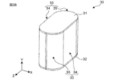
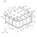
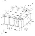
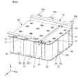
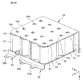
- FIG. 1 is a perspective view schematically showing a capacitor module 1 according to a first embodiment of the present invention.
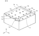
- FIG. 2 is a plan view of the capacitor module 1 of FIG.
- FIG. 3A is a perspective view showing a first capacitor 20 included in the first capacitor group 12 of the capacitor module 1 of FIG.
- FIG. 3B is a perspective view showing a second capacitor 30 included in the second capacitor group 13 of the capacitor module 1 of FIG.
- FIG. 4 is a perspective view showing a first bus bar 14 and a second bus bar 15 included in the capacitor module 1 of FIG.
- FIG. 5 is a perspective view showing a third bus bar 16 included in the capacitor module 1 of FIG.
- FIG. 6 is a perspective view showing an insulating member 18 included in the capacitor module 1 of FIG. FIG.
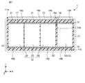
- FIG. 7 is a cross-sectional view of the capacitor module 1 of FIG. 2 in the AA direction.
- FIG. 8 is an enlarged view of a part of FIG. 7.
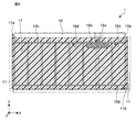
- FIG. 9 is a cross-sectional view of the capacitor module 1 of FIG. 2 in the BB direction.
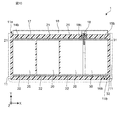
- FIG. 10 is a cross-sectional view of the capacitor module 1 of FIG. 2 in the CC direction.
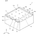
- FIG. 11A is an enlarged perspective view of a part of the capacitor module 1 of FIG.
- FIG. 11B is a perspective view in which the insulating member 18 of the capacitor module 1 of FIG. 11A is omitted.
- the X, Y, and Z directions in the drawing indicate the horizontal direction, the height direction, and the vertical direction of the capacitor module 1, respectively.
- the capacitor module 1 includes a case 11, a first capacitor group 12, a second capacitor group 13, a first bus bar 14, a second bus bar 15, and a third bus bar 16. , A sealing resin 17 and an insulating member 18. In FIG. 2, the sealing resin 17 is not shown.
- the case 11 has an opening 11a (see FIG. 1) formed at a position facing the bottom surface 11b (see FIG. 7).
- a first capacitor group 12, a second capacitor group 13, a first bus bar 14, a second bus bar 15, a third bus bar 16, and an insulating member 18 are housed inside the case 11, and the case 11 is sealed.
- the resin 17 is filled.
- the capacitor module 1 is formed so that each of the first bus bar 14, the second bus bar 15, and the third bus bar 16 extends outward along the side surface of the case 11.
- the first bus bar 14, the second bus bar 15, and the third bus bar 16 have terminal portions 14a, 15a, and 16a for connecting external elements and circuits, respectively.
- the first capacitor group 12 is an aggregate of capacitors including a plurality of first capacitors 20 shown in FIG. 3A.
- the second capacitor group 13 is an aggregate of capacitors including one or a plurality of second capacitors 30 shown in FIG. 3B. Since the first capacitor group 12 and the second capacitor group 13 have different functions (for example, capacitance), the capacitor module 1 has two functions. In this embodiment, as shown in FIG. 2, the first capacitor group 12 includes six first capacitors 20, and the second capacitor group 13 includes two second capacitors 30.
- the first capacitor 20 and the second capacitor 30 are wound film capacitors, respectively.
- the first capacitor 20 has a first electrode 21, a second electrode 22, and a side surface 23 connecting the first electrode 21 and the second electrode 22.
- the second capacitor 30 has a third electrode 31, a fourth electrode 32, and a side surface 33 connecting the third electrode 31 and the fourth electrode 32.
- the first bus bar 14 and the second bus bar 15 are arranged on the opening side of the case 11.
- the opening side of the case 11 refers to the side inside the case 11 that is closer to the opening 11a than the bottom surface 11b.
- the first bus bar 14 is connected to the first electrode 21 of each first capacitor 20.
- the second bus bar 15 is connected to the third electrode 31 of each second capacitor 30.
- a plate-shaped third bus bar 16 is arranged on the bottom surface side of the case 11.
- the bottom surface side of the case 11 refers to the side inside the case 11 that is closer to the bottom surface 11b than the opening 11a.
- a first capacitor 20 and a second capacitor 30, respectively, are arranged on the third bus bar 16.
- the second electrode 22 of each first capacitor 20 and the fourth electrode 32 of each second capacitor 30 are connected to the third bus bar 16. That is, each of the first capacitors 20 is arranged so that the first electrode 21 faces the opening side and the second electrode 22 faces the bottom surface side.
- each of the second capacitors 30 is arranged so that the third electrode faces the opening side and the fourth electrode 32 faces the bottom surface side.
- An insulating member 18 is arranged between the first bus bar 14 and the second bus bar 15.
- the insulating member 18 insulates the first electrode 21 and the first bus bar 14 of the first capacitor 20 from the third electrode 31 and the second bus bar 15 of the second capacitor 30.
- the first capacitor 20 is a winding type film capacitor.
- the first capacitor 20 is formed by winding a dielectric film having a metal vapor deposition film formed on its surface and pressing the wound body of the dielectric film into a flat shape. Therefore, as shown in FIG. 2A, the side surface 23 of the first capacitor 20 has a pair of flat portions 24 facing each other and a pair of curved portions 25 connecting the pair of flat portions 24 to each other.
- the dielectric film of the first capacitor 20 for example, a plastic film such as polyethylene terephthalate, polypropylene, polyphenylene sulfide, or polyethylene naphthalate can be used. Further, Al, Zn or the like can be used as the metal vapor deposition film formed on the surface of the plastic film.
- the first electrode 21 and the second electrode 22 are formed by spraying, for example, Zn or the like on the end of the wound dielectric film.
- the first bus bar 14 is a conductive member connected to the first electrode 21 of each of the first capacitors 20 of the first capacitor group 12. As shown in FIG. 4, the first bus bar 14 has a terminal portion 14a connected to an external element or circuit of the capacitor module 1 and an electrode contact portion 14b in contact with each of the first electrodes 21.
- the terminal portion 14a and the electrode contact portion 14b are integrally formed by bending one metal plate.
- the first bus bar 14 is formed of a conductive metal such as Al, Cu, or brass.
- the electrode contact portion 14b is formed with a hole 14c for connecting the first electrodes 21 with solder.
- the terminal portion 14a extends from the electrode contact portion 14b in the height direction (Y direction), and is further bent in the vertical direction (Z direction) in the vicinity of the opening 11a of the case 11.
- the second bus bar 15 is a conductive member connected to the third electrode 31 of each of the second capacitors 30 of the second capacitor group 13. As shown in FIG. 4, the second bus bar 15 has a terminal portion 15a connected to an external element or circuit of the capacitor module 1 and an electrode contact portion 15b in contact with each of the third electrodes 31.
- the terminal portion 15a and the electrode contact portion 15b are integrally formed by bending one metal plate.
- the second bus bar 15 is formed of a conductive metal such as Al, Cu, or brass.
- the electrode contact portion 15b is formed with a hole 15c for connecting each third electrode 31 with solder.
- the terminal portion 15a extends from the electrode contact portion 15b in the height direction (Y direction), and is further bent in the vertical direction (Z direction) in the vicinity of the opening 11a of the case 11.
- the first bus bar 14 and the second bus bar 15 are arranged at intervals d in the lateral direction (X direction) in order to electrically insulate them as shown in FIG. 8 to be described later.
- the third bus bar 16 is connected to the second electrode 22 of each of the first capacitors 20 of the first capacitor group 12 and the fourth electrode 32 of each of the second capacitors 30 of the second capacitor group 13. As shown in FIG. 5, the third bus bar 16 has a terminal portion 16a, an electrode contact portion 16b, and an extending portion 16c.
- the terminal portion 16a is connected to an element or circuit outside the capacitor module 1.
- the electrode contact portion 16b is in common contact with the second electrode 22 and the fourth electrode 32.
- the extending portion 16c extends outward from the electrode contact portion 16b along the side surface of the case 11.
- the terminal portion 16a, the electrode contact portion 16b, and the extending portion 16c are integrally formed by bending a single piece of metal.
- the third bus bar 16 is formed of a conductive metal such as Al, Cu, or brass.
- the electrode contact portion 16b is formed with a hole 16d for connecting the second electrode 22 and the fourth electrode 32, respectively, by soldering.
- the extending portion 16c extends in the height direction (Y direction) from the electrode contact portion 16b, and is bent in the vertical direction (Z direction) near the opening 11a of the case 11.
- a through hole 16e is formed in the extending portion 16c of the third bus bar.
- the through hole 16e is for inserting the insulating member 18 in the ⁇ Y direction.
- the insulating member 18 is a member that insulates the first bus bar 14 and the first electrode 21 and the second bus bar 15 and the third electrode 31.
- the first bus bar 14 and the first electrode 21 and the second bus bar 15 and the third electrode 31 can be more reliably insulated.
- the insulating member 18 has a plate-shaped first portion 18a and a second portion 18b extending so as to intersect the first portion 18a.
- the insulating member 18 is formed of an electrically insulating resin such as polyphenylene sulfide (PPS resin) or polybutylene terephthalate (PBT resin). Since the insulating member 18 is formed by injection molding, it is preferable to use a resin suitable for injection molding.
- the first portion 18a of the insulating member 18 is arranged along between the electrode contact portion 14b of the first bus bar 14 and the electrode contact portion 15b of the second bus bar 15.
- one end 19a of the first portion 18a is an electrode contact portion of the first bus bar 14 in the direction from the opening 11a toward the bottom surface 11b, that is, in the height direction (Y direction). It is located on the opening side of the electrode contact portion 15b of the 14b and the second bus bar 15. Further, the other end 19b of the second portion 18b is located on the bottom surface side of the first electrode 21 and the third electrode 31.
- the distance between the first bus bar 14 and the second bus bar 15 is reduced as compared with the case where the insulating member 18 is not arranged. Insulation distances i1 and i2 between the bus bars can be secured.
- the arrows i1 and i2 shown in FIG. 8 are the insulation distances i1 and i2 between the first bus bar 14 and the first electrode 21 and the second bus bar 15 and the third electrode 31.
- the distance d between the first bus bar 14 and the second bus bar 15 is the insulation distance, so that the distance d must be increased, which makes it difficult to miniaturize the capacitor module 1.
- the insulating member 18 As in the present embodiment, it is possible to secure the insulating distance while reducing the distance d between the first bus bar 14 and the second bus bar 15. Therefore, the first bus bar 14 and the first electrode 21 and the second bus bar 15 and the third electrode 31 can be more reliably insulated.
- the insulation distances i1 and i2 may be set to appropriate values in consideration of the maximum applied voltage of the capacitor groups 12 and 13.
- the insulation distance can be changed by adjusting the positions of one end 19a and the other end 19b of the first portion 18a of the insulating member 18 in the height direction.
- the second portion 18b of the insulating member 18 is the surface 14d of the electrode contact portion 14b of the first bus bar 14 on the side of the first electrode 21 and the second portion 15b of the electrode contact portion 15b of the second bus bar 15. It is located on the bottom surface side of the case 11 with respect to the surface 15d on the 3 electrode 31 side. That is, the second portion 18b of the insulating member 18 is arranged on the lower side of the first bus bar 14 and the second bus bar 15 in the height direction. By arranging the second portion 18b below the first bus bar 14 and the second bus bar 15, it is possible to prevent the insulating member 18 from being lifted by the buoyancy of the sealing resin 17.
- the second portion 18b of the insulating member 18 is arranged between the adjacent curved portions 25 of the adjacent first capacitor 20 and the adjacent curved portions 35 of the adjacent second capacitor 30. .. Since the first capacitor 20 has a curved portion 25, a space is created between the adjacent curved portions 25 of the adjacent first capacitor 20. Similarly, in the case of the second capacitor 30, a space is created between the adjacent curved portions 35.
- the second portion 18b of the insulating member 18 is arranged using this space, the second portion 18b of the insulating member 18 can be arranged without enlarging the case 11, and the insulating member 18 can be insulated while effectively utilizing the space. It is possible to prevent the sex member 18 from rising.
- the first portion 18a of the insulating member 18 is provided with a third portion 18c for preventing misalignment in the horizontal direction including the horizontal direction (X direction) and the vertical direction (Z direction).
- Notches 14e and 15e are provided in the electrode contact portions 14b of the first bus bar 14 and the electrode contact portions 15b of the second bus bar 15, respectively, in order to create a space for arranging the third portion 18c.
- the third portion 18c is arranged so as to be placed on a part of the first electrode 21 and a part of the third electrode 31.
- the third portion 18c of the insulating member 18 is arranged on the upper side of the first capacitor 20 and the second capacitor 30 in the height direction, and is surrounded by the cutouts 14e and 15e so that the insulating member 18 can be placed in the vertical direction ( It is possible to prevent the displacement in the Z direction) or the lateral direction (Z direction).
- the insulating member 18 can be restricted from moving in the + Y direction by the second portion 18b, and can be regulated from moving in the X and Z directions by the third portion 18c.
- the case 11 houses each component of the capacitor module 1.
- the case 11 has an opening 11a formed at a position facing the bottom surface 11b.
- the case 11 has a substantially square opening 11a and a bottom surface 11b, and has a box shape.
- the shape of the case 11 is not limited to this, and various shapes can be taken depending on the arrangement of the capacitor groups.
- the case 11 is formed of, for example, a synthetic resin such as polyphenylene sulfide (PPS resin) or polybutylene terephthalate (PBT resin).
- the case 11 is formed with a protrusion 11c for positioning the insulating member 18.
- the protrusion 11c is a protrusion formed from the inner side surface of the case 11 toward the inside, and forms a recess 11d that receives the first portion 18a of the insulating member 18 in the direction from the opening 11a toward the bottom surface 11b.
- the movement of the protrusion 11c and the insulating member 18 in the lateral direction (X direction) and the vertical direction (Z direction) is restricted. That is, the insulating member 18 is positioned in the X direction and the Z direction by the protrusion 11c.
- the shape of the protrusion 11c is not limited to that shown in FIGS. 11A and 11B, and may be any shape that can hold the end portion of the insulating member 18.
- the movement of the insulating member 18 in the X direction and the Z direction is restricted. Further, the movement of the insulating member 18 in the ⁇ Y direction is also restricted. Since the sealing resin 17 is filled around the insulating member 18, the insulating member 18 is positioned by the protrusion 11c of the case 11 and the sealing resin 17.
- the through hole 16e of the third bus bar 16 overlaps with the protrusion 11c of the case 11.
- the insulating member 18 can be inserted in the direction from the opening 11a toward the bottom surface 11b.
- the bottom surface 11b of the case 11 is flat.
- the sealing resin 17 can easily spread over the entire bottom surface 11b as compared with the case where the bottom surface 11b is provided with a convex portion, so that the filling property of the sealing resin 17 is improved. be able to.
- the sealing resin 17 is filled in the case 11 to seal each component of the capacitor module 1.
- the sealing resin 17 is a thermosetting resin, and for example, an epoxy resin can be used. Alternatively, it may be urethane resin.
- FIGS. 12A to 12F are diagrams showing a manufacturing process of the capacitor module 1 according to the first embodiment.
- the third bus bar 16 can be formed by, for example, pressing a metal plate.
- insulating paper 41 is attached to the extending portion 16c of the third bus bar 16. back.
- the first capacitor 20 and the second capacitor 30 are arranged on the electrode contact portion 16b of the third bus bar 16, respectively. Specifically, as shown in FIG. 12A, the first capacitor 20 and the second capacitor 30, respectively, are arranged so that the second electrode 22 and the fourth electrode 32 face the electrode contact portion 16b.
- the insulating member 18 is arranged. Specifically, as shown in FIG. 12B, the first portion 18a of the insulating member 18 is arranged between the first capacitor group 12 and the second capacitor group 13. At this time, the second portion 18b is located between the curved portions 25 of the first capacitor 20 and between the curved portions 35 of the second capacitor 30. Further, the third portion 18c is placed on the first capacitor 20 and the second capacitor 30.
- the first portion 18a of the insulating member 18 is arranged so as to be sandwiched between the first capacitor group 12 and the second capacitor group 13, and lateral movement is possible. Be regulated. Further, at this time, since the end portion of the first portion 18a passes through the through hole 16e of the third bus bar, the first portion 18a and the third bus bar 16 do not interfere with each other.
- the insulating member 18 is not in a fixed state, but is arranged so that the end portion of the insulating member 18 can be fitted into the recess 11d in the step of inserting each component described later into the case 11. ing.
- the second portion 18b is located in the ⁇ Y direction with respect to the first electrode 21 and the third electrode 31, the insulating member 18 is in a state of being movable in the Y direction, so that the insulating member 18 is fitted into the recess 11d.
- the combination can be easily performed.
- the first bus bar 14 and the second bus bar 15 are arranged. Specifically, as shown in FIG. 12C, the electrode contact portion 14b of the first bus bar 14 is placed on the first electrode 21 of each first capacitor 20 of the first capacitor group 12. Further, the electrode contact portion 15b of the second bus bar 15 is placed on the third electrode 31 of each of the second capacitors 30 of the second capacitor group 13. At this time, the first bus bar 14 and the second bus bar 15 are arranged so that the third portion 18c of the insulating member 18 is located in the notches 14e and 15e of the first bus bar 14 and the second bus bar 15, respectively. ..
- the electrode contact portion 14b and each of the first electrodes 21 are connected by soldering (not shown). Further, in the hole 15c of the electrode contact portion 15b of the second bus bar 15, the electrode contact portion 15b and each of the third electrodes 31 are connected by solder (not shown). By soldering, the first bus bar 14 and each of the first electrodes 21 and the second bus bar 15 and each of the third electrodes 31 can be electrically connected.
- the third bus bar 16 is connected to the second electrode 22 and the fourth electrode 32, respectively, by soldering (not shown). Specifically, as shown in FIG. 12D, the third bus bar 16, the second electrode 22, and the fourth electrode are soldered in the holes 16d provided in the electrode contact portion 16b of the third bus bar 16. It is electrically connected to 32.
- the soldered first capacitor 20, the second capacitor 30, the first bus bar 14, the second bus bar 15, the third bus bar 16, and the insulating member 18 are attached to the case 11. insert.
- the end portion of the first portion 18a of the insulating member 18 is inserted into the recess 11d of the protrusion 11c of the case 11 (see FIG. 11A).
- the insulating member 18 is positioned in the X direction and the Z direction inside the case 11.
- the case 11 After being inserted into the case 11, as shown in FIG. 12F, the case 11 is filled with the sealing resin 17 and the sealing resin 17 is cured to complete the capacitor module 1. At this time, the second portion 18b of the insulating member 18 is restricted from moving in the + Y direction by the first bus bar 14 and the second bus bar 15 (see FIG. 9). Therefore, it is possible to prevent the insulating member 18 from floating when the sealing resin 17 is filled. Further, since the bottom surface 11b of the case 11 is formed flat, the filling property of the sealing resin 17 is improved.
- the capacitor module 1 includes a case 11, a first capacitor group 12, a second capacitor group 13, a first bus bar 14, a second bus bar 15, a third bus bar 16, a sealing resin 17, and an insulating member. It is provided with 18.
- the case 11 has an opening 11a formed at a position facing the bottom surface 11b.
- the first capacitor group 12 includes one or more first capacitors 20.
- the first capacitor 20 is arranged inside the case 11 and has a first electrode 21, a second electrode 22, and a side surface 23 connecting the first electrode 21 and the second electrode 22.
- the second capacitor group 13 includes one or more second capacitors 30.
- the second capacitor 30 is arranged inside the case 11 and has a third electrode 31, a fourth electrode 32, and a side surface 23 connecting the third electrode 31 and the fourth electrode 32.
- the first bus bar 14 is arranged inside the case 11 on the opening 11a side with respect to the first capacitor group 12, and has an electrode contact portion 14b that contacts the first electrode 21.
- the second bus bar 15 is arranged inside the case 11 on the opening 11a side with respect to the second capacitor group 13, and has an electrode contact portion 15b that contacts the third electrode 31.
- the third bus bar 16 is arranged on the bottom surface 11b side with respect to the first capacitor group 12 and the second capacitor group 13 inside the case 11, and is in common contact with the second electrode 22 and the fourth electrode 32. It has a part 16b.
- the sealing resin 17 is filled in the case 11.
- the insulating member 18 is provided between the electrode contact portion 14b of the first bus bar 14 and the electrode contact portion 15b of the second bus bar 15, and is surrounded by the sealing resin 17.
- the first bus bar 14, the first electrode 21, and the second bus bar 15 are compared with the case where the insulating member 18 is not arranged and only the sealing resin 17 is provided. And the insulation property with the third electrode 31 can be improved.
- the insulating member 18 is not arranged, it is insulated by the sealing resin 17, but there is a risk of insulation failure due to air bubbles generated in the sealing resin 17.
- the first bus bar 14 and the first electrode 21 and the second bus bar 15 and the third electrode 31 can be reliably insulated, and the insulating property can be improved. improves.
- the insulating member 18 By arranging the insulating member 18, long insulation distances i1 and i2 are secured while reducing the distance d between the first bus bar 14 and the first electrode 21 and the second bus bar 15 and the third electrode 31. be able to. Therefore, the distance d between the first bus bar 14 and the first electrode 21 and the second bus bar 15 and the third electrode 31 can be reduced, which contributes to the miniaturization of the capacitor module 1.
- one end 19a of the insulating member 18 opens the case 11 more than the electrode contact portion 14b of the first bus bar 14 and the electrode contact portion 15b of the second bus bar 15 in the direction from the opening 11a toward the bottom surface 11b.
- the other end 19b of the insulating member 18 is located on the bottom surface side of the case 11 with respect to the first electrode 21 and the third electrode 31.
- the insulation distances of the first bus bar 14 and the second bus bar 15 can be changed depending on the positions of the ends 19a and 19b of the insulating member 18 in the height direction (Y direction).
- Y direction the height direction
- the insulation distance i1 becomes longer.
- the position of the other end 19b of the insulating member 18 in the height direction is located below FIG. 8 (-Y direction)
- the insulation distance i2 becomes longer.
- the lengths of the insulation distances i1 and i2 may be appropriately set according to the capacitance of the capacitor module 1 and the like.
- the insulating distance is the electrode contact portion 14b.
- the distance d from the electrode contact portion 15b in order to secure an appropriate insulation distance, the distance d is increased, which makes it difficult to reduce the size of the capacitor module 1.
- the insulation distance is determined by the first electrode 21 and the third electrode 31.
- the distance d from the third electrode 31 in this case as well, the distance d is increased in order to secure an appropriate insulation distance.
- a protrusion 11c is formed on the inner surface of the case 11 to have a recess 11d that receives the insulating member 18 in the direction from the opening 11a toward the bottom surface 11b, and to position the insulating member 18.
- the third bus bar 16 further has an extending portion 16c extending from the electrode contact portion 16b of the third bus bar 16 to the outside of the case 11 through the opening 11a along the side surface of the case 11.
- a through hole 16e through which the insulating member 18 is passed is formed in the extending portion 16c.
- the insulating member 18 has a first portion 18a and a second portion 18b.
- the first portion 18a extends along between the electrode contact portion 14b of the first bus bar 14 and the electrode contact portion 15b of the second bus bar 15.
- the second portion 18b extends so as to intersect the first portion 18a, and the surface 14d of the electrode contact portion 14b of the first bus bar 14 on the side of the first electrode 21 and the electrode contact portion 15b of the second bus bar 15. It extends so as to be located on the bottom surface side of the case 11 with respect to the surface 15d on the third electrode 31 side. With such a configuration, it is possible to prevent the insulating member 18 from being lifted by the buoyancy of the sealing resin 17.
- the side surface 23 of the first capacitor 20 has a pair of flat portions 24 facing each other and a pair of curved portions 25 connecting the pair of flat portions 24 to each other.
- the side surface 33 of the second capacitor 30 has a pair of flat portions 34 and a pair of curved portions 35 connecting the pair of flat portions 34 to each other.
- the second portion 18b of the insulating member 18 is arranged between the adjacent curved portions 25 of the adjacent first capacitor 20 and between the adjacent curved portions 35 of the adjacent second capacitor 30. With such a configuration, the second portion 18b can be arranged in the space formed between the adjacent curved portions 25 and the adjacent curved portions 35, which contributes to the miniaturization of the capacitor module 1.
- the bottom surface 11b of the case 11 is flat. With such a configuration, the filling property of the sealing resin 17 can be improved.
- the bottom surface 11b of the case 11 is flat, the fluidity of the resin is improved, so that the flow of the resin when filling the case with the resin is blocked, which reduces the time required for the resin filling process and increases the manufacturing cost. It is possible to prevent it from being lost.
- the case 11 can be easily manufactured, so that the size can be reduced, which contributes to the miniaturization of the capacitor module 1.
- the present invention is not limited to this.
- the second portion 18b may extend to either the first capacitor group 12 side or the second capacitor group 13 side. Further, the second portion 18b may be provided at two or more places.
- the insulating member 18 is provided with the second portion 18b and the third portion 18c has been described, but the second portion 18b and the third portion 18c may not be provided.
- the notches 14e and 15e of the first bus bar 14 and the second bus bar 15, respectively may not be formed.
- the insulating member 18 is positioned by the protrusion 11c of the case 11, but not limited to such a case, as shown in FIGS. 13A and 13B, the insulating member 18 is formed in the through hole of the third bus bar 16. May be positioned.
- FIG. 13A is an enlarged perspective view of a part of the capacitor module 1a according to the modified example of the first embodiment of the present invention.
- FIG. 13B is a perspective view in which the insulating member 18 of the capacitor module 1a of FIG. 13A is omitted.
- the sealing resin 17 is omitted.
- the insulating member 18 is formed at one end on the bottom surface side of the through hole 16f formed in the extending portion 16c. It is received by the bus bar 16 and positioned.
- the through hole 16f is formed with a portion whose width decreases from the opening side toward the bottom surface side and a portion having a substantially constant width similar to that of the insulating member 18.
- the insulating member 18 is positioned at a portion having a certain width. Therefore, when the insulating member 18 is inserted from the opening side to the bottom surface side, the insulating member 18 is positioned in the lateral direction (X direction).
- the insulating member 18 can be positioned with a simple configuration, and the manufacturing cost is reduced. Can be reduced. Further, when the through hole 16f as shown in FIGS. 13A and 13B is provided, the insulating member 18 is already positioned in the state of FIG. 12B. Therefore, as shown in FIG. 12E, it is possible to prevent the insulating member 18 from being displaced with respect to the bus bar or the capacitor when it is inserted into the case 11. Therefore, the positioning accuracy of the insulating member 18 is improved, and the insulating property can be improved.
- the second embodiment mainly describes the differences from the first embodiment.
- the same or equivalent configurations as those in the first embodiment will be described with the same reference numerals. Further, in the second embodiment, the description overlapping with the first embodiment is omitted.
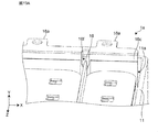
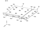
- FIG. 14 is a perspective view in which the case and the sealing resin of the capacitor module 1b according to the second embodiment are omitted.
- FIG. 15 is an enlarged view of the region R1 of the capacitor module 1b of FIG.
- FIG. 16 is a diagram showing an insulating member 58 of the capacitor module 1b of FIG.
- FIG. 17 is a diagram showing a first bus bar 54 and a second bus bar 55 of the capacitor module 1b of FIG.
- the second portion 58b of the insulating member 58 has a protrusion 58c, and the protrusion 58c is provided on each of the first bus bar 54 and the second bus bar 55, respectively. It differs from the first embodiment in that it is inserted into the holes 54e and 55e (see FIG. 17).
- the insulating member 58 has two second portions 58b at both ends of the first portion 58a. That is, four second portions 58b are formed in the first portion 58a. Further, a protrusion 58c is formed from each second portion 58b of the insulating member 58 in the + Y direction. The tip of the protrusion 58c is formed in a hook shape.
- holes 54e and 55e are formed in the first bus bar 54 and the second bus bar 55, respectively.
- the hook portion of the protrusion 58c is caught in the hole 54e or 55e. It is fixed. That is, each of the protrusion 58c and the hole 54e or 55e is fitted by snap-fitting. In this way, the insulating member 58 is joined to the first bus bar 54 and the second bus bar 55.
- the insulating member 58 is joined to and positioned with the first bus bar 54 and the second bus bar 55. Therefore, the case 11 and the third bus bar 16 are not formed with protrusions or through holes for positioning the insulating member 58. Further, since the insulating member 18, the first bus bar 54, and the second bus bar 55 are fitted by snap-fitting, the insulating member 58 has a portion for preventing lifting (second portion 18b of the first embodiment). ) Is not provided, and the configuration is simpler than that of the first embodiment.
- FIGS. 18A to 18F are diagrams showing a manufacturing process of the capacitor module 1b according to the second embodiment.
- the first bus bar 54 and the second bus bar 55 are prepared.
- the first bus bar 54 is formed with an electrode contact portion 54b, a terminal portion 54a, a hole 54c for soldering, and a hole 54e for joining with the insulating member 58.
- the second bus bar 55 is formed with an electrode contact portion 55b, a terminal portion 55a, a hole 55c for soldering, and a hole 55e for joining with the insulating member 58.
- the protrusion 58c of the insulating member 58 is inserted into the hole 54e of the first bus bar 54 and the hole 55e of the second bus bar 55.
- Each of the protrusions 58c of the insulating member 58 is inserted in the direction (Y direction) from the bottom surface 11b of the case 11 toward the opening 11a. Since the insulating member 58 is joined to the first bus bar 54 and the second bus bar 55 by snap-fitting, the insulating member 58 can be firmly fixed to the first bus bar 54 and the second bus bar 55.
- the electrode contact portion 54b of the first bus bar 54 and the electrode contact portion 15b of the second bus bar 55 are kept substantially in the same plane. Can be fixed while.
- each of the first capacitor 20 and the second capacitor 30 is arranged at the electrode contact portion 16b of the third bus bar 16.
- the first bus bar 54 and the second bus bar 55 joined to the insulating member 58 in FIG. 18B are arranged on the first capacitor 20 and the second capacitor 30.
- the insulating member 58 does not have to be arranged in the through hole of the third bus bar 16, and the first bus bar 54 and the second bus bar 55 are kept substantially in the same plane. , Can be easily placed.
- first bus bar 54 and the second bus bar 55 After arranging the first bus bar 54 and the second bus bar 55, the first bus bar 54 and the first electrode 21 of each of the first capacitors 20 and the second bus bar 55 and the third electrode 31 of each second capacitor 30 are placed. Connect by solder (not shown). The first bus bar 54 and each of the first electrodes 21 are electrically connected by soldering in the holes 54c provided in the electrode contact portion 54b of the first bus bar 54. Similarly, both the second bus bar 55 and the third electrode 31 are electrically soldered to the second bus bar 55 and the third electrode 31 by soldering them in the holes 55c provided in the electrode contact portion 55b of the second bus bar 55. Connect to.
- the third bus bar 16 and the respective second electrodes 22 and fourth electrodes 32 are connected by solder (not shown).
- the third bus bar 16 is electrically connected to the second electrode 22 and the fourth electrode 32 by soldering in the hole 16d provided in the electrode contact portion 16b of the third bus bar 16.
- the soldered first capacitor 20, second capacitor 30, first bus bar 54, second bus bar 55, third bus bar 16, and insulating member 58 are inserted into the case 11. At this time, no protrusion is formed on the case 11, and the insulating member 58 and the case 11 do not need to be aligned with each other, so that the case 11 can be easily arranged.
- the case 11 After being inserted into the case 11, as shown in FIG. 18G, the case 11 is filled with the sealing resin 17 and the sealing resin 17 is cured to complete the capacitor module 1b. At this time, the protrusions 58c of the insulating member 58 are inserted into the holes 54e and 55e, respectively. Therefore, it is possible to prevent the insulating member 58 from being lifted by the buoyancy of the sealing resin 17 without separately providing a lift prevention structure (second portion 18b of the first embodiment) of the insulating member 58.
- the second portion 58b of the insulating member 58 of the capacitor module 1b has a protrusion 58c and is inserted into holes 54e and 55e provided in the first bus bar 54 and the second bus bar 55, respectively.
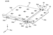
- the capacitor module 1c according to the modified example of the second embodiment will be described with reference to FIGS. 19 to 21.
- FIG. 19 is a perspective view in which the case and the sealing resin of the capacitor module 1c according to the modified example of the second embodiment are omitted.
- FIG. 20 is an enlarged view of the region R2 of the capacitor module 1c of FIG.
- FIG. 21 is a diagram showing a first bus bar 64, a second bus bar 65, and an insulating member 68 of the capacitor module 1c of FIG.
- the insulating member 58 and the first bus bar 54 and the second bus bar 55 are joined by a snap-fit structure, but in the capacitor module 1c, they are joined by screws.
- the insulating member 68 and the first bus bar 64 and the second bus bar 65 are joined by four screws 69.
- the second portion 68b of the insulating member 68 has a recess 68c.
- circular holes 64e and 65e are provided in the first bus bar 64 and the second bus bar 65, respectively.
- the capacitor module 1c further has screws 69 to be inserted into holes 64e and 65e and recesses 68c provided in the first bus bar 64 and the second bus bar 65, respectively.
- the insulating member 68, the first bus bar 64, and the second bus bar 65 can be fixed more firmly than the snap fit. Further, the positioning accuracy of the insulating member 68 can be improved.
- the present invention is useful for capacitors used in various electronic devices, electrical devices, industrial devices, vehicle devices, and the like.
Abstract
絶縁性を向上したコンデンサモジュールを提供する。コンデンサモジュールは、底面および開口部を有するケースと、第1電極と、第2電極と、第1電極と第2電極とを繋ぐ側面と、をそれぞれ有する1つまたは複数の第1コンデンサを含む第1コンデンサグループと、第3電極と、第4電極と、第3電極と第4電極とを繋ぐ側面と、をそれぞれ有する1つまたは複数の第2コンデンサを含む第2コンデンサグループと、第1電極に接触する電極接触部を有する板状の第1バスバーと、第3電極に接触する電極接触部を有する板状の第2バスバーと、第2電極および第4電極に共通して接触する電極接触部を有する第3バスバーと、ケース内に充填される封止樹脂と、第1バスバーの電極接触部と、第2バスバーの電極接触部との間に設けられ封止樹脂によって囲まれる絶縁性部材と、を備える。
Description
本発明は、コンデンサモジュールに関する。
表面に金属膜が設けられた誘電体フィルムを巻回または積層されて形成される1つまたは複数のコンデンサをケースに収容し、各コンデンサの両端の電極にバスバーを接続したコンデンサモジュールが知られている。
例えば、特許文献1には、ケースの底面に設けられた仕切板により、コンデンサ素子と電子部品とを隔離して収納したフィルムコンデンサが開示されている。
特許文献1に記載のフィルムコンデンサは、絶縁性の向上という点で未だ改善の余地がある。
そこで、本発明は、絶縁性を向上したコンデンサモジュールを提供することを目的とする。
本発明の一態様にかかるコンデンサモジュールは、
底面に対向する位置に開口部が形成されたケースと、
前記ケース内の内部に配置され、第1電極と、第2電極と、前記第1電極と前記第2電極とを繋ぐ側面と、をそれぞれ有する1つまたは複数の第1コンデンサを含む第1コンデンサグループと、
前記ケース内の内部に配置され、第3電極と、第4電極と、前記第3電極と前記第4電極とを繋ぐ側面と、をそれぞれ有する1つまたは複数の第2コンデンサを含む第2コンデンサグループと、
前記ケースの内部において、前記第1コンデンサグループに対して前記開口部側に配置され、前記第1電極に接触する電極接触部を有する板状の第1バスバーと、
前記ケースの内部において、前記第2コンデンサグループに対して前記開口部側に配置され、前記第3電極に接触する電極接触部を有する板状の第2バスバーと、
前記ケースの内部において、前記第1コンデンサグループおよび前記第2コンデンサグループに対して前記底面側に配置され、前記第2電極および前記第4電極に共通して接触する電極接触部を有する第3バスバーと、
前記ケース内に充填される封止樹脂と、
前記第1バスバーの前記電極接触部と、前記第2バスバーの前記電極接触部との間に設けられ、前記封止樹脂によって囲まれる絶縁性部材と、
を備える。
本発明によると、絶縁性を向上したコンデンサモジュールを提供することができる。
(本発明に至った経緯)
機能の異なる2以上のコンデンサグループを有するコンデンサモジュールが知られている。例えば、1つのケースに、それぞれのコンデンサグループが収容され、ケース内に絶縁性樹脂が充填されたコンデンサモジュールがある。それぞれのコンデンサグループには1つ以上のコンデンサが含まれている。それぞれのコンデンサグループは、ケース内に充填された絶縁性樹脂により絶縁されている。しかし、このような構成の場合、絶縁性樹脂内に発生した気泡により、絶縁性が低下するという課題がある。
機能の異なる2以上のコンデンサグループを有するコンデンサモジュールが知られている。例えば、1つのケースに、それぞれのコンデンサグループが収容され、ケース内に絶縁性樹脂が充填されたコンデンサモジュールがある。それぞれのコンデンサグループには1つ以上のコンデンサが含まれている。それぞれのコンデンサグループは、ケース内に充填された絶縁性樹脂により絶縁されている。しかし、このような構成の場合、絶縁性樹脂内に発生した気泡により、絶縁性が低下するという課題がある。
そこで、本発明者らは、2以上のコンデンサグループを有するコンデンサモジュールにおいて、コンデンサグループ間の絶縁性を向上させる構成について検討し、以下の発明に至った。
本発明の一態様にかかるコンデンサモジュールは、
底面に対向する位置に開口部が形成されたケースと、
前記ケース内の内部に配置され、第1電極と、第2電極と、前記第1電極と前記第2電極とを繋ぐ側面と、をそれぞれ有する1つまたは複数の第1コンデンサを含む第1コンデンサグループと、
前記ケース内の内部に配置され、第3電極と、前記底面側に配置される第4電極と、前記第3電極と前記第4電極とを繋ぐ側面と、をそれぞれ有する1つまたは複数の第2コンデンサを含む第2コンデンサグループと、
前記ケースの内部において、前記第1コンデンサグループに対して前記開口部側に配置され、前記第1電極に接触する電極接触部を有する板状の第1バスバーと、
前記ケースの内部において、前記第2コンデンサグループに対して前記開口部側に配置され、前記第3電極に接触する電極接触部を有する板状の第2バスバーと、
前記ケースの内部において、前記第1コンデンサグループおよび前記第2コンデンサグループに対して前記底面側に配置され、前記第2電極および前記第4電極に共通して接触する電極接触部を有する第3バスバーと、
前記ケース内に充填される封止樹脂と、
前記第1バスバーの前記電極接触部と、前記第2バスバーの前記電極接触部との間に設けられ、前記封止樹脂によって囲まれる絶縁性部材と、
を備える。
この構成によると、絶縁性を向上したコンデンサモジュールを提供することができる。
前記絶縁性部材は、前記開口部から前記底面に向かう方向において、一方の端部が前記第1バスバーの前記電極接触部および前記第2バスバーの前記電極接触部よりも前記開口部側に位置し、他方の端部が前記第1電極および前記第3電極よりも前記底面側に位置するよう配置されてもよい。
この構成によると、第1コンデンサグループと第2コンデンサグループとの距離を小さくしつつ、それぞれのコンデンサグループの絶縁距離を確保することができる。このため、絶縁性を向上しつつ、コンデンサモジュールの小型化を実現することができる。
前記ケースの内側面に、前記絶縁性部材を、前記開口部から前記底面に向かう方向に受ける凹部が形成されてもよい。
この構成によると、ケース内での絶縁性部材の位置ずれを防止することができる。
前記第3バスバーは、前記第3バスバーの前記電極接触部から前記ケースの側面に沿って、前記開口部を介して前記ケースの外側へ延びる延在部をさらに有し、前記延在部に前記絶縁性部材を通す貫通孔が形成されていてもよい。
この構成によると、第3バスバーと絶縁性部材の干渉を防止することができる。
前記絶縁性部材は、前記貫通孔の前記底面側の一端で前記第3バスバーに受けられて位置決めされてもよい。
この構成によると、ケースに凹部を設けなくてもよいため、製造コストを低減することができる。
前記絶縁性部材は、
前記第1バスバーの前記電極接触部と、前記第2バスバーの前記電極接触部との間に沿って延在する第1部分と、
前記第1部分に対して交差するように延びて前記第1バスバーの前記電極接触部の前記第1電極側の面および前記第2バスバーの前記電極接触部の前記第3電極側の面に対して、前記ケースの前記底面側に位置するように延びる第2部分と、
を有してもよい。
前記第1バスバーの前記電極接触部と、前記第2バスバーの前記電極接触部との間に沿って延在する第1部分と、
前記第1部分に対して交差するように延びて前記第1バスバーの前記電極接触部の前記第1電極側の面および前記第2バスバーの前記電極接触部の前記第3電極側の面に対して、前記ケースの前記底面側に位置するように延びる第2部分と、
を有してもよい。
この構成によると、絶縁性部材の封止樹脂の浮力による浮き上がりを防止することができる。
前記第1コンデンサの側面および前記第2コンデンサの側面はそれぞれ、互いに対向する一対の扁平部と、前記一対の扁平部どうしを繋ぐ一対の湾曲部と、を有し、
前記絶縁性部材の前記第2部分は、隣接する前記第1コンデンサの隣接する前記湾曲部の間および隣接する前記第2コンデンサの隣接する前記湾曲部の間に配置されてもよい。
前記絶縁性部材の前記第2部分は、隣接する前記第1コンデンサの隣接する前記湾曲部の間および隣接する前記第2コンデンサの隣接する前記湾曲部の間に配置されてもよい。
この構成によると、コンデンサ間の空いたスペースに第2部分を配置することができるため、コンデンサモジュールの小型化に寄与する。
前記絶縁性部材の前記第2部分は突起を有し、
前記突起が前記第1バスバーおよび前記第2バスバーのそれぞれに設けられた孔に挿入されてもよい。
前記突起が前記第1バスバーおよび前記第2バスバーのそれぞれに設けられた孔に挿入されてもよい。
この構成によると、絶縁性部材の位置決めを容易に行うことができる。
前記絶縁性部材の前記第2部分は凹部を有し、
前記第1バスバーおよび前記第2バスバーのそれぞれに設けられた孔および前記凹部に挿入されるねじをさらに備えてもよい。
前記第1バスバーおよび前記第2バスバーのそれぞれに設けられた孔および前記凹部に挿入されるねじをさらに備えてもよい。
この構成によると、絶縁性部材の位置決めを容易に行うことができる。
前記ケースの前記底面が平坦であってもよい。
この構成によると、封止樹脂の充填性を向上することができる。
以下、本発明にかかる実施の形態1について、添付の図面を参照しながら説明する。また、各図においては、説明を容易なものとするため、各要素を誇張して示している。
(実施の形態1)
図1は、本発明の実施の形態1にかかるコンデンサモジュール1を概略的に示す斜視図である。図2は、図1のコンデンサモジュール1の平面図である。図3Aは、図1のコンデンサモジュール1の第1コンデンサグループ12に含まれる第1コンデンサ20を示す斜視図である。図3Bは、図1のコンデンサモジュール1の第2コンデンサグループ13に含まれる第2コンデンサ30を示す斜視図である。図4は、図1のコンデンサモジュール1に含まれる第1バスバー14および第2バスバー15を示す斜視図である。図5は、図1のコンデンサモジュール1に含まれる第3バスバー16を示す斜視図である。図6は、図1のコンデンサモジュール1に含まれる絶縁性部材18を示す斜視図である。図7は、図2のコンデンサモジュール1のA-A方向の断面図である。図8は、図7の一部を拡大した図である。図9は、図2のコンデンサモジュール1のB-B方向の断面図である。図10は、図2のコンデンサモジュール1のC-C方向の断面図である。図11Aは、図1のコンデンサモジュール1の一部を拡大した斜視図である。図11Bは、図11Aのコンデンサモジュール1の絶縁性部材18を省略した斜視図である。なお、図中のX、Y、Z方向はそれぞれ、コンデンサモジュール1の横方向、高さ方向、縦方向を示す。
図1は、本発明の実施の形態1にかかるコンデンサモジュール1を概略的に示す斜視図である。図2は、図1のコンデンサモジュール1の平面図である。図3Aは、図1のコンデンサモジュール1の第1コンデンサグループ12に含まれる第1コンデンサ20を示す斜視図である。図3Bは、図1のコンデンサモジュール1の第2コンデンサグループ13に含まれる第2コンデンサ30を示す斜視図である。図4は、図1のコンデンサモジュール1に含まれる第1バスバー14および第2バスバー15を示す斜視図である。図5は、図1のコンデンサモジュール1に含まれる第3バスバー16を示す斜視図である。図6は、図1のコンデンサモジュール1に含まれる絶縁性部材18を示す斜視図である。図7は、図2のコンデンサモジュール1のA-A方向の断面図である。図8は、図7の一部を拡大した図である。図9は、図2のコンデンサモジュール1のB-B方向の断面図である。図10は、図2のコンデンサモジュール1のC-C方向の断面図である。図11Aは、図1のコンデンサモジュール1の一部を拡大した斜視図である。図11Bは、図11Aのコンデンサモジュール1の絶縁性部材18を省略した斜視図である。なお、図中のX、Y、Z方向はそれぞれ、コンデンサモジュール1の横方向、高さ方向、縦方向を示す。
[全体構成]
コンデンサモジュール1は、図1および図2に示すように、ケース11と、第1コンデンサグループ12と、第2コンデンサグループ13と、第1バスバー14と、第2バスバー15と、第3バスバー16と、封止樹脂17と、絶縁性部材18と、を備える。なお、図2では、封止樹脂17が図示省略されている。
コンデンサモジュール1は、図1および図2に示すように、ケース11と、第1コンデンサグループ12と、第2コンデンサグループ13と、第1バスバー14と、第2バスバー15と、第3バスバー16と、封止樹脂17と、絶縁性部材18と、を備える。なお、図2では、封止樹脂17が図示省略されている。
ケース11は、底面11b(図7参照)に対向する位置に開口部11a(図1参照)が形成されている。ケース11の内部には、第1コンデンサグループ12、第2コンデンサグループ13、第1バスバー14、第2バスバー15、第3バスバー16、および絶縁性部材18が収容され、ケース11内には封止樹脂17が充填されている。
また、コンデンサモジュール1は、第1バスバー14、第2バスバー15、第3バスバー16のそれぞれがケース11の側面に沿って外部に延びて形成される。第1バスバー14、第2バスバー15、第3バスバー16はそれぞれ、外部の素子や回路を接続する端子部14a、15a、16aを有する。
第1コンデンサグループ12は、図3Aに示す第1コンデンサ20を複数含むコンデンサの集合体である。第2コンデンサグループ13は、図3Bに示す第2コンデンサ30を1つまたは複数含むコンデンサの集合体である。第1コンデンサグループ12と第2コンデンサグループ13とは異なる機能(例えば、静電容量)を有するため、コンデンサモジュール1は2つの機能を有する。本実施の形態では、図2に示すように、第1コンデンサグループ12は6つの第1コンデンサ20を含み、第2コンデンサグループ13は2つの第2コンデンサ30を含む。
第1コンデンサ20および第2コンデンサ30はそれぞれ、巻回型フィルムコンデンサである。第1コンデンサ20は、図3Aに示すように、第1電極21と、第2電極22と、第1電極21と第2電極22とを繋ぐ側面23とを有する。第2コンデンサ30は、図3Bに示すように、第3電極31と、第4電極32と、第3電極31と第4電極32とを繋ぐ側面33とを有する。
図1に戻って、ケース11の開口部側に、第1バスバー14および第2バスバー15が配置される。なお、ケース11の開口部側とは、ケース11の内部において、底面11bよりも開口部11aに近い側を示す。第1バスバー14は、それぞれの第1コンデンサ20の第1電極21に接続される。第2バスバー15は、それぞれの第2コンデンサ30の第3電極31に接続される。
ケース11の底面側には、板状の第3バスバー16が配置される。なお、ケース11の底面側とは、ケース11の内部において、開口部11aよりも底面11bに近い側を示す。第3バスバー16上には、それぞれの第1コンデンサ20および第2コンデンサ30が配置される。それぞれの第1コンデンサ20の第2電極22と、それぞれの第2コンデンサ30の第4電極32とが、第3バスバー16に接続される。すなわち、それぞれの第1コンデンサ20は、第1電極21が開口部側、第2電極22が底面側に向くよう配置される。同様に、それぞれの第2コンデンサ30は、第3電極が開口部側、第4電極32が底面側に向くよう配置される。
第1バスバー14と第2バスバー15との間には、絶縁性部材18が配置される。絶縁性部材18により、第1コンデンサ20の第1電極21および第1バスバー14と、第2コンデンサ30の第3電極31および第2バスバー15とが絶縁されている。
以下、コンデンサモジュール1のそれぞれの構成要素について詳細に説明する。
<コンデンサ>
第1コンデンサ20および第2コンデンサ30は同様の構成であるため、ここでは、第1コンデンサ20についてのみ説明する。第1コンデンサ20は、巻回型のフィルムコンデンサである。第1コンデンサ20は、表面に金属蒸着膜を形成した誘電体フィルムを巻回し、誘電体フィルムの巻回体を扁平形状にプレスすることにより形成される。このため、第1コンデンサ20の側面23は、図2Aに示すように、互いに対向する一対の扁平部24と、一対の扁平部24どうしを繋ぐ一対の湾曲部25と、を有する。
第1コンデンサ20および第2コンデンサ30は同様の構成であるため、ここでは、第1コンデンサ20についてのみ説明する。第1コンデンサ20は、巻回型のフィルムコンデンサである。第1コンデンサ20は、表面に金属蒸着膜を形成した誘電体フィルムを巻回し、誘電体フィルムの巻回体を扁平形状にプレスすることにより形成される。このため、第1コンデンサ20の側面23は、図2Aに示すように、互いに対向する一対の扁平部24と、一対の扁平部24どうしを繋ぐ一対の湾曲部25と、を有する。
第1コンデンサ20の誘電体フィルムとして、例えば、ポリエチレンテレフタレート、ポリプロピレン、ポリフェニレンサルファイド、またはポリエチレンナフタレート等のプラスチックフィルムを使用することができる。また、プラスチックフィルムの表面に形成される金属蒸着膜としては、Al、Zn等を使用することができる。巻回した誘電体フィルムの端部に、例えばZn等を溶射することにより第1電極21および第2電極22が形成される。
<第1バスバー>
第1バスバー14は、第1コンデンサグループ12のそれぞれの第1コンデンサ20の第1電極21に接続される導電性部材である。図4に示すように、第1バスバー14は、コンデンサモジュール1の外部の素子または回路等に接続される端子部14aと、それぞれの第1電極21に接触する電極接触部14bと、を有する。
第1バスバー14は、第1コンデンサグループ12のそれぞれの第1コンデンサ20の第1電極21に接続される導電性部材である。図4に示すように、第1バスバー14は、コンデンサモジュール1の外部の素子または回路等に接続される端子部14aと、それぞれの第1電極21に接触する電極接触部14bと、を有する。
端子部14aおよび電極接触部14bは、1枚の金属板を折り曲げて一体的に形成されている。第1バスバー14は、Al、Cu、または真鍮等の導電性を有する金属により形成される。また、電極接触部14bには、それぞれの第1電極21を半田により接続するための穴14cが形成されている。端子部14aは、電極接触部14bから高さ方向(Y方向)に延在し、さらにケース11の開口部11aの付近で縦方向(Z方向)に屈曲されて形成されている。
<第2バスバー>
第2バスバー15は、第2コンデンサグループ13のそれぞれの第2コンデンサ30の第3電極31に接続される導電性部材である。図4に示すように、第2バスバー15は、コンデンサモジュール1の外部の素子または回路等に接続される端子部15aと、それぞれの第3電極31に接触する電極接触部15bと、を有する。
第2バスバー15は、第2コンデンサグループ13のそれぞれの第2コンデンサ30の第3電極31に接続される導電性部材である。図4に示すように、第2バスバー15は、コンデンサモジュール1の外部の素子または回路等に接続される端子部15aと、それぞれの第3電極31に接触する電極接触部15bと、を有する。
端子部15aおよび電極接触部15bは、1枚の金属板を折り曲げて一体的に形成されている。第2バスバー15は、Al、Cu、または真鍮等の導電性を有する金属により形成される。また、電極接触部15bには、それぞれの第3電極31を半田により接続するための穴15cが形成されている。端子部15aは、電極接触部15bから高さ方向(Y方向)に延在し、さらにケース11の開口部11aの付近で縦方向(Z方向)に屈曲されて形成されている。
第1バスバー14と第2バスバー15とは、後述する図8に示すように電気的に絶縁するため、横方向(X方向)において、間隔dをあけて配置される。
<第3バスバー>
第3バスバー16は、第1コンデンサグループ12のそれぞれの第1コンデンサ20の第2電極22と、第2コンデンサグループ13のそれぞれの第2コンデンサ30の第4電極32とに接続される。第3バスバー16は、図5に示すように、端子部16aと、電極接触部16bと、延在部16cと、を有する。端子部16aは、コンデンサモジュール1の外部の素子または回路に接続される。電極接触部16bは、第2電極22と第4電極32とに共通して接触する。延在部16cは、電極接触部16bからケース11の側面に沿って外側へ延びる。
第3バスバー16は、第1コンデンサグループ12のそれぞれの第1コンデンサ20の第2電極22と、第2コンデンサグループ13のそれぞれの第2コンデンサ30の第4電極32とに接続される。第3バスバー16は、図5に示すように、端子部16aと、電極接触部16bと、延在部16cと、を有する。端子部16aは、コンデンサモジュール1の外部の素子または回路に接続される。電極接触部16bは、第2電極22と第4電極32とに共通して接触する。延在部16cは、電極接触部16bからケース11の側面に沿って外側へ延びる。
端子部16a、電極接触部16b、および延在部16cは、一枚の金属を折り曲げて一体的に形成されている。第3バスバー16は、Al、Cu、または真鍮等の導電性を有する金属により形成される。また、電極接触部16bには、それぞれの第2電極22および第4電極32を半田により接続するための穴16dが形成されている。延在部16cは、電極接触部16bから高さ方向(Y方向)に延在し、ケース11の開口部11a付近で縦方向(Z方向)に屈曲される。
図5に示すように、第3バスバーの延在部16cには貫通孔16eが形成されている。貫通孔16eは、絶縁性部材18を-Y方向に向かって挿入するためのものである。
<絶縁性部材>
絶縁性部材18は、図1および図2に示すように、第1バスバー14および第1電極21と、第2バスバー15および第3電極31とを絶縁する部材である。絶縁性部材18を配置することにより、第1バスバー14および第1電極21と第2バスバー15および第3電極31とをより確実に絶縁することができる。
絶縁性部材18は、図1および図2に示すように、第1バスバー14および第1電極21と、第2バスバー15および第3電極31とを絶縁する部材である。絶縁性部材18を配置することにより、第1バスバー14および第1電極21と第2バスバー15および第3電極31とをより確実に絶縁することができる。
絶縁性部材18は、図6に示すように、板状の第1部分18aと、第1部分18aに沿って交差するように延びる第2部分18bとを有する。絶縁性部材18は、例えば、ポリフェニレンサルファイド(PPS樹脂)、ポリブチレンテレフタレート(PBT樹脂)等の電気絶縁性を有する樹脂により形成される。絶縁性部材18は、射出成形により形成するため、射出成形に適した樹脂を使用するとよい。
絶縁性部材18の第1部分18aは、図1および図2に示すように、第1バスバー14の電極接触部14bと第2バスバー15の電極接触部15bとの間に沿って配置される。第1部分18aは、図7および図8に示すように、開口部11aから底面11bに向かう方向、すなわち高さ方向(Y方向)において、一方の端部19aが第1バスバー14の電極接触部14bおよび第2バスバー15の電極接触部15bよりも開口部側に位置する。また、第2部分18bの他方の端部19bは、第1電極21および第3電極31よりも底面側に位置する。
絶縁性部材18の第1部分18aがこのように配置されることにより、絶縁性部材18を配置しない場合と比較して、第1バスバー14と第2バスバー15との距離を小さくしつつ、それぞれのバスバー間の絶縁距離i1、i2を確保することができる。本実施の形態では、図8に示す矢印i1、i2が、第1バスバー14および第1電極21と、第2バスバー15および第3電極31との絶縁距離i1、i2となる。
絶縁性部材18を配置しない場合、第1バスバー14と第2バスバー15との間隔dが絶縁距離となるため間隔dを大きくしなくてはならず、コンデンサモジュール1の小型化が困難になる。本実施の形態のように、絶縁性部材18を配置することにより、第1バスバー14と第2バスバー15との間隔dを小さくしつつ、絶縁距離を確保することができる。このため、第1バスバー14および第1電極21と、第2バスバー15および第3電極31とをより確実に絶縁することができる。
絶縁距離i1、i2は、コンデンサグループ12、13の最大印加電圧を考慮して、適切な値を設定するとよい。絶縁性部材18の第1部分18aの一方の端部19aおよび他方の端部19bの高さ方向の位置を調整することにより、絶縁距離を変更することができる。
また、絶縁性部材18の第2部分18bは、図9に示すように、第1バスバー14の電極接触部14bの第1電極21側の面14dおよび第2バスバー15の電極接触部15bの第3電極31側の面15dに対して、ケース11の底面側に位置する。すなわち、絶縁性部材18の第2部分18bが第1バスバー14および第2バスバー15の高さ方向における下側に配置される。第2部分18bが第1バスバー14および第2バスバー15の下側に配置されることにより、封止樹脂17の浮力により、絶縁性部材18が浮き上がるのを防止することができる。
図2に戻って、絶縁性部材18の第2部分18bは、隣接する第1コンデンサ20の隣接する湾曲部25の間と、隣接する第2コンデンサ30の隣接する湾曲部35とに配置される。第1コンデンサ20が湾曲部25を有する形状であるため、隣接する第1コンデンサ20の隣接する湾曲部25の間にスペースが生じる。第2コンデンサ30の場合も同様に、隣接する湾曲部35の間にスペースが生じる。このスペースを利用して、絶縁性部材18の第2部分18bを配置すると、ケース11を大きくすることなく絶縁性部材18の第2部分18bを配置することができ、スペースを有効活用しつつ絶縁性部材18の浮き上がりを防止することができる。
また、本実施の形態では、絶縁性部材18の第1部分18aに、横方向(X方向)および縦方向(Z方向)を含む水平方向における位置ずれを防止する第3部分18cが設けられている。第3部分18cを配置するスペースを作るため、第1バスバー14の電極接触部14bと第2バスバー15の電極接触部15bにはそれぞれ、切欠き部14e、15eが設けられている。第3部分18cは、図10に示すように、第1電極21の一部および第3電極31の一部に載置されるよう配置される。絶縁性部材18の第3部分18cは、第1コンデンサ20および第2コンデンサ30の高さ方向における上側に配置され、切欠き部14e、15eに囲まれることにより、絶縁性部材18が縦方向(Z方向)または横方向(Z方向)にずれるのを防止することができる。
上述したように、絶縁性部材18は、第2部分18bにより、+Y方向の移動を規制し、第3部分18cにより、X方向およびZ方向への移動を規制することができる。
<ケース>
ケース11は、コンデンサモジュール1のそれぞれの構成要素を収容する。本実施の形態では、ケース11は、底面11bに対向する位置に開口部11aが形成されている。本実施の形態では、ケース11は、略正方形の開口部11aおよび底面11bを有し、箱型の形状である。ケース11の形状はこれに限定されず、コンデンサグループの配置によって、様々な形状を取り得る。ケース11は、例えば、ポリフェニレンサルファイド(PPS樹脂)、ポリブチレンテレフタレート(PBT樹脂)等の合成樹脂等により形成される。
ケース11は、コンデンサモジュール1のそれぞれの構成要素を収容する。本実施の形態では、ケース11は、底面11bに対向する位置に開口部11aが形成されている。本実施の形態では、ケース11は、略正方形の開口部11aおよび底面11bを有し、箱型の形状である。ケース11の形状はこれに限定されず、コンデンサグループの配置によって、様々な形状を取り得る。ケース11は、例えば、ポリフェニレンサルファイド(PPS樹脂)、ポリブチレンテレフタレート(PBT樹脂)等の合成樹脂等により形成される。
図11Aおよび図11Bに示すように、ケース11には、絶縁性部材18を位置決めする突起11cが形成されている。突起11cは、ケース11の内側面から内側に向かって形成された突起部であり、絶縁性部材18の第1部分18aを開口部11aから底面11bに向かう方向に受ける凹部11dを形成する。突起11c、絶縁性部材18の横方向(X方向)および縦方向(Z方向)への移動を規制する。すなわち、突起11cにより、絶縁性部材18がX方向およびZ方向に位置決めされる。突起11cの形状は、図11Aおよび図11Bに示すものに限らず、絶縁性部材18の端部を保持できる形状であればよい。
突起11cに絶縁性部材18の第1部分18aを配置すると、絶縁性部材18のX方向およびZ方向の移動が規制される。さらに、絶縁性部材18の-Y方向への移動も規制される。絶縁性部材18の周囲には、封止樹脂17が充填されるため、ケース11の突起11cと封止樹脂17とにより、絶縁性部材18が位置決めされる。
図11Aおよび図11Bに示すように、第3バスバー16をケース11に配置したときに、第3バスバー16の貫通孔16eが、ケース11の突起11cと重なる。第3バスバー16の貫通孔16eとケース11の突起11cとがこのような配置となるよう形成されることで、絶縁性部材18を開口部11aから底面11bに向かう方向に挿入することができる。
また、図7、図9、図10に示すように、ケース11の底面11bは平坦である。ケース11の底面11bを平坦にすることにより、底面11bに凸部を設ける場合と比較して、封止樹脂17が底面11bの全体に広がりやすくなるため、封止樹脂17の充填性を向上することができる。
<封止樹脂>
封止樹脂17は、ケース11内に充填されて、コンデンサモジュール1のそれぞれの構成要素を封止する。封止樹脂17は、熱硬化性の樹脂であり、例えばエポキシ樹脂を使用することができる。または、ウレタン樹脂であってもよい。封止樹脂17の材料としては、流動性および接着性の高い材料を使用するとよい。
封止樹脂17は、ケース11内に充填されて、コンデンサモジュール1のそれぞれの構成要素を封止する。封止樹脂17は、熱硬化性の樹脂であり、例えばエポキシ樹脂を使用することができる。または、ウレタン樹脂であってもよい。封止樹脂17の材料としては、流動性および接着性の高い材料を使用するとよい。
[製造方法]
コンデンサモジュール1の製造方法について図12A~図12Fを参照して説明する。図12A~図12Fは、実施の形態1にかかるコンデンサモジュール1の製造工程を示す図である。
コンデンサモジュール1の製造方法について図12A~図12Fを参照して説明する。図12A~図12Fは、実施の形態1にかかるコンデンサモジュール1の製造工程を示す図である。
まず、第3バスバー16を用意する。図5に示すように、第3バスバー16は、例えば、金属板をプレス加工することにより形成することができる。第3バスバー16と、それぞれの第1コンデンサ20の第1電極21および第2コンデンサ30の第3電極31とを絶縁するため、第3バスバー16の延在部16cに絶縁紙41を貼付しておく。
次に、第3バスバー16の電極接触部16bに、それぞれの第1コンデンサ20および第2コンデンサ30を配置する。具体的には、図12Aに示すように、第2電極22および第4電極32が電極接触部16bに向くよう、それぞれの第1コンデンサ20および第2コンデンサ30を配置する。
次に、絶縁性部材18を配置する。具体的には、図12Bに示すように、絶縁性部材18の第1部分18aが、第1コンデンサグループ12と第2コンデンサグループ13との間に配置される。このとき、第2部分18bが第1コンデンサ20の湾曲部25の間および第2コンデンサ30の湾曲部35の間に位置する。また、第3部分18cが第1コンデンサ20および第2コンデンサ30に載置される。このように絶縁性部材18を配置することにより、絶縁性部材18の第1部分18aは、第1コンデンサグループ12と第2コンデンサグループ13との間に挟まるように配置され、横方向の移動が規制される。また、このとき、第1部分18aの端部は、第3バスバーの貫通孔16eを通過するため、第1部分18aと第3バスバー16とは干渉しない。
図12Bにおいて、絶縁性部材18は固定されている状態ではなく、後述するそれぞれの構成要素をケース11に挿入する工程において、絶縁性部材18の端部を凹部11dに嵌めることができるよう配置されている。このとき、第2部分18bが、第1電極21および第3電極31よりも-Y方向に位置することにより、絶縁性部材18がY方向に移動可能な状態となるため、凹部11dへの嵌合を容易に行うことができる。
次に、第1バスバー14と第2バスバー15とを配置する。具体的には、図12Cに示すように、第1バスバー14の電極接触部14bを、第1コンデンサグループ12のそれぞれの第1コンデンサ20の第1電極21に載置する。また、第2バスバー15の電極接触部15bを、第2コンデンサグループ13のそれぞれの第2コンデンサ30の第3電極31に載置する。このとき、第1バスバー14および第2バスバー15のそれぞれの切欠き部14e、15eに、絶縁性部材18の第3部分18cが位置するよう、第1バスバー14と第2バスバー15とを配置する。
その後、第1バスバー14の電極接触部14bの穴14cにおいて、電極接触部14bとそれぞれの第1電極21とを半田(図示省略)により接続する。また、第2バスバー15の電極接触部15bの穴15cにおいて、電極接触部15bとそれぞれの第3電極31を半田(図示省略)により接続する。半田付けを行うことにより、第1バスバー14とそれぞれの第1電極21と、および、第2バスバー15とそれぞれの第3電極31と、を電気的に接続することができる。
次に、第3バスバー16と、それぞれの第2電極22および第4電極32とを半田(図示省略)により接続する。具体的には、図12Dに示すように、第3バスバー16の電極接触部16bに設けられた穴16dにおいて、半田付けを行うことにより、第3バスバー16と、第2電極22および第4電極32とを電気的に接続する。
次に、図12Eに示すように、半田付けしたそれぞれの第1コンデンサ20、第2コンデンサ30、第1バスバー14、第2バスバー15、第3バスバー16、および絶縁性部材18を、ケース11に挿入する。このとき、絶縁性部材18の第1部分18aの端部が、ケース11の突起11cの凹部11dに挿入されるようにする(図11A参照)。第1部分18aの端部が突起11cに挿入されると、ケース11の内部で絶縁性部材18がX方向およびZ方向に位置決めされる。
ケース11に挿入した後、図12Fに示すように、ケース11内に封止樹脂17を充填し、封止樹脂17を硬化させてコンデンサモジュール1が完成する。このとき、絶縁性部材18の第2部分18bが、第1バスバー14および第2バスバー15により+Y方向への移動を規制される(図9参照)。このため、封止樹脂17を充填する際の、絶縁性部材18の浮き上がりを防止することができる。また、ケース11の底面11bが平坦に形成されているため、封止樹脂17の充填性が向上する。
[効果]
実施の形態1にかかるコンデンサモジュール1によれば、以下の効果を奏することができる。
実施の形態1にかかるコンデンサモジュール1によれば、以下の効果を奏することができる。
コンデンサモジュール1は、ケース11と、第1コンデンサグループ12と、第2コンデンサグループ13と、第1バスバー14と、第2バスバー15と、第3バスバー16と、封止樹脂17と、絶縁性部材18とを備える。ケース11は、底面11bに対向する位置に開口部11aが形成されている。第1コンデンサグループ12は、1つまたは複数の第1コンデンサ20を含む。第1コンデンサ20は、ケース11の内部に配置され、第1電極21と、第2電極22と、第1電極21と第2電極22とを繋ぐ側面23と、を有する。第2コンデンサグループ13は、1つまたは複数の第2コンデンサ30を含む。第2コンデンサ30は、ケース11の内部に配置され、第3電極31と、第4電極32と、第3電極31と第4電極32とを繋ぐ側面23と、を有する。第1バスバー14は、ケース11の内部において、第1コンデンサグループ12に対して開口部11a側に配置され、第1電極21に接触する電極接触部14bを有する板状である。第2バスバー15は、ケース11の内部において、第2コンデンサグループ13に対して開口部11a側に配置され、第3電極31に接触する電極接触部15bを有する板状である。第3バスバー16は、ケース11の内部において、第1コンデンサグループ12および第2コンデンサグループ13に対して底面11b側に配置され、第2電極22および第4電極32に共通して接触する電極接触部16bを有する。封止樹脂17は、ケース11内に充填される。絶縁性部材18は、第1バスバー14の電極接触部14bと、第2バスバー15の電極接触部15bとの間に設けられ、封止樹脂17によって囲まれる。
このような構成により、絶縁性部材18を設けることで、絶縁性部材18が配置されず封止樹脂17のみの場合と比較して、第1バスバー14および第1電極21と、第2バスバー15および第3電極31との絶縁性を向上することができる。絶縁性部材18が配置されていない場合、封止樹脂17により絶縁されるが、封止樹脂17に発生した気泡により絶縁不良の恐れがある。封止樹脂17とは別に、絶縁性部材18を設けることで、第1バスバー14および第1電極21と、第2バスバー15および第3電極31とを確実に絶縁することができ、絶縁性が向上する。
また、絶縁性部材18を配置することにより、第1バスバー14および第1電極21と、第2バスバー15および第3電極31との距離dを小さくしつつ、長い絶縁距離i1、i2を確保することができる。このため、第1バスバー14および第1電極21と、第2バスバー15および第3電極31との間隔dを小さくすることができ、コンデンサモジュール1の小型化に寄与する。
また、絶縁性部材18の一方の端部19aは、開口部11aから底面11bに向かう方向において、第1バスバー14の電極接触部14bおよび第2バスバー15の電極接触部15bよりもケース11の開口部側に位置する。また、絶縁性部材18の他方の端部19bは、第1電極21および第3電極31よりもケース11の底面側に位置する。このような構成により、適切な絶縁距離を確保することができる。
絶縁性部材18の端部19a、19bの高さ方向(Y方向)の位置により、第1バスバー14および第2バスバー15の絶縁距離を変更することができる。図8を参照して、一方の端部19aの高さ方向の位置を、図8よりも上(+Y方向)に位置するようにすると、絶縁距離i1はより長くなる。同様に、絶縁性部材18の他方の端部19bの高さ方向の位置を、図8よりも下(-Y方向)に位置するようにすると、絶縁距離i2はより長くなる。このように、コンデンサモジュール1の静電容量等に応じて、絶縁距離i1、i2の長さを適切に設定するとよい。
一方、絶縁性部材18の一方の端部19aの高さ方向の位置が、第1バスバー14および第2バスバー15よりも下(-Y方向)に位置する場合、絶縁距離は電極接触部14bと電極接触部15bとの距離dである。この場合、適切な絶縁距離を確保するため、距離dを大きくすることになり、コンデンサモジュール1の小型化が困難になる。同様に、絶縁性部材18の他方の端部19bの高さ方向の位置が、第1電極21および第3電極31よりも下(+Y方向)にある場合、絶縁距離は、第1電極21および第3電極31との距離dである。この場合も適切な絶縁距離を確保するため、距離dを大きくすることとなる。実施の形態1のように、絶縁性部材18を配置することで、絶縁性を確保しつつ、距離dを小さくすることができるため、コンデンサモジュール1の小型化に寄与する。
ケース11の内側面に、絶縁性部材18を、開口部11aから底面11bに向かう方向に受ける凹部11dを有し、絶縁性部材18を位置決めする突起11cが形成される。このような構成により、ケース11内での絶縁性部材18の位置ずれを防止することができ、より確実に絶縁することができる。
また、第3バスバー16は、第3バスバー16の電極接触部16bからケース11の側面に沿って、開口部11aを介してケース11の外側へ延びる延在部16cをさらに有する。延在部16cには、絶縁性部材18を通す貫通孔16eが形成されている。このような構成により、第3バスバー16と絶縁性部材18との干渉を防止することができる。
また、絶縁性部材18は、第1部分18aと、第2部分18bと、を有する。第1部分18aは、第1バスバー14の電極接触部14bと、第2バスバー15の電極接触部15bとの間に沿って延在する。第2部分18bは、第1部分18aに対して交差するように延びて、第1バスバー14の電極接触部14bの第1電極21側の面14d、および第2バスバー15の電極接触部15bの第3電極31側の面15dに対して、ケース11の底面側に位置するように延びる。このような構成により、絶縁性部材18の封止樹脂17の浮力による浮き上がりを防止することができる。
また、第1コンデンサ20の側面23は、互いに対向する一対の扁平部24と、一対の扁平部24どうしを繋ぐ一対の湾曲部25と、を有する。第2コンデンサ30の側面33は、一対の扁平部34と、一対の扁平部34どうしを繋ぐ一対の湾曲部35と、を有する。絶縁性部材18の第2部分18bは、隣接する第1コンデンサ20の隣接する湾曲部25の間、および隣接する第2コンデンサ30の隣接する湾曲部35の間に配置される。このような構成により、隣接する湾曲部25の間、および隣接する湾曲部35の間にできるスペースに第2部分18bを配置することができ、コンデンサモジュール1の小型化に寄与する。
また、ケース11の底面11bが平坦である。このような構成により、封止樹脂17の充填性を向上することができる。ケース11の底面11bが平坦である場合、樹脂の流動性が向上するため、ケースに樹脂を充填する際の樹脂の流動が遮られることにより樹脂の充填加工に時間が下がり、製造コストが増加してしまうことを防止することができる。また、ケース11の底面11bが平坦である場合、ケース11の製造が容易になるため小型化を図ることができ、ひいてはコンデンサモジュール1の小型化に寄与する。
[変形例]
なお、実施の形態1では、第1コンデンサグループ12が6つの第1コンデンサ20を含み、第2コンデンサグループ13が2つの第2コンデンサ30を含む例について説明したが、これに限定されない。第1コンデンサグループ12および第2コンデンサグループ13に含まれるコンデンサの数は、1つ以上であればよい。
なお、実施の形態1では、第1コンデンサグループ12が6つの第1コンデンサ20を含み、第2コンデンサグループ13が2つの第2コンデンサ30を含む例について説明したが、これに限定されない。第1コンデンサグループ12および第2コンデンサグループ13に含まれるコンデンサの数は、1つ以上であればよい。
実施の形態1では、絶縁性部材18の第2部分18bが、第1コンデンサグループ12側と第2コンデンサグループ13側との双方に延びている例について説明したが、これに限定されない。第2部分18bは、第1コンデンサグループ12側または第2コンデンサグループ13側のいずれか一方に延びていればよい。また、第2部分18bが2か所以上設けられていてもよい。
実施の形態1では、絶縁性部材18に第2部分18b、第3部分18cが設けられている例について説明したが、第2部分18bおよび第3部分18cは設けられていなくてもよい。絶縁性部材18に第3部分18cが設けられていない場合、第1バスバー14および第2バスバー15のそれぞれの切欠き部14e、15eは形成されなくてもよい。
実施の形態1では、ケース11の突起11cにより絶縁性部材18を位置決めしたが、このような場合に限らず、図13A、13Bに示すように、第3バスバー16の貫通孔において絶縁性部材18を位置決めしてもよい。図13Aは、本発明の実施の形態1の変形例にかかるコンデンサモジュール1aの一部を拡大した斜視図である。図13Bは、図13Aのコンデンサモジュール1aの絶縁性部材18を省略した斜視図である。図13A~13Bにおいて、封止樹脂17が省略されている。
図13A~図13Bに示すように、コンデンサモジュール1aにおいては、ケース11に突起が形成されず、絶縁性部材18が、延在部16cに形成された貫通孔16fの底面側の一端で第3バスバー16に受けられて位置決めされる。貫通孔16fは、開口部側から底面側に向かうにつれて、幅が小さくなる部分と、絶縁性部材18と略同じ一定の幅を有する部分と、が形成されている。絶縁性部材18は、一定の幅を有する部分で位置決めされる。このため、開口部側から底面側に絶縁性部材18を差し込んだときに、絶縁性部材18は横方向(X方向)に位置決めされる。
このような構成によると、ケース11に突起を形成しなくてもよく、第3バスバー16の形状を変更するだけでよいため簡単な構成で絶縁性部材18を位置決めすることができ、製造コストを削減することができる。また図13A、13Bのような貫通孔16fを有する場合、図12Bの状態において、絶縁性部材18がすでに位置決めされる。このため、図12Eのように、ケース11に挿入する際に、バスバーまたはコンデンサに対する絶縁性部材18の位置ずれを防止することができる。このため、絶縁性部材18の位置決め精度が向上し、絶縁性を向上させることができる。
(実施の形態2)
本発明の実施の形態2にかかるコンデンサモジュール1bについて説明する。
本発明の実施の形態2にかかるコンデンサモジュール1bについて説明する。
実施の形態2では、主に実施の形態1と異なる点について説明する。実施の形態2においては、実施の形態1と同一または同等の構成については同じ符号を付して説明する。また、実施の形態2では、実施の形態1と重複する記載は省略する。
図14は、実施の形態2にかかるコンデンサモジュール1bのケースおよび封止樹脂を省略した斜視図である。図15は、図14のコンデンサモジュール1bの領域R1を拡大した図である。図16は、図14のコンデンサモジュール1bの絶縁性部材58を示す図である。図17は、図14のコンデンサモジュール1bの第1バスバー54および第2バスバー55を示す図である。
実施の形態2では、図14および図15に示すように、絶縁性部材58の第2部分58bが突起58cを有し、突起58cが第1バスバー54および第2バスバー55のそれぞれに設けられた孔54e、55e(図17参照)に挿入される点で、実施の形態1と異なる。
絶縁性部材58は、図16に示すように、第1部分58aの両端に2つずつ第2部分58bを有する。すなわち、第1部分58aに4つの第2部分58bが形成されている。また、絶縁性部材58のそれぞれの第2部分58bから+Y方向に向かって、突起58cが形成されている。突起58cは、先端がフック状に形成されている。
また、図17に示すように、第1バスバー54および第2バスバー55には、それぞれ孔54e、55eが形成されている。絶縁性部材58の第2部分58bのそれぞれの突起58cが、第1バスバー54の孔54eまたは第2バスバー55の孔55eに挿入されることにより、突起58cのフック部分が孔54eまたは55eに引っ掛かり固定される。すなわち、突起58cと孔54eまたは55eのそれぞれがスナップフィットにより嵌合する。このようにして、絶縁性部材58と、第1バスバー54および第2バスバー55とが接合される。
なお、本実施の形態では、絶縁性部材58は、第1バスバー54および第2バスバー55と接合され、位置決めされる。このため、ケース11および第3バスバー16には絶縁性部材58の位置決めのための突起または貫通孔が形成されていない。また、絶縁性部材18と第1バスバー54および第2バスバー55とがスナップフィットにより嵌合しているため、絶縁性部材58には、浮き上がりを防止する部分(実施の形態1の第2部分18b)が設けられず、実施の形態1よりも簡素な構成となっている。
[製造方法]
コンデンサモジュール1bの製造方法について図18A~図18Fを参照して説明する。図18A~図18Fは、実施の形態2にかかるコンデンサモジュール1bの製造工程を示す図である。
コンデンサモジュール1bの製造方法について図18A~図18Fを参照して説明する。図18A~図18Fは、実施の形態2にかかるコンデンサモジュール1bの製造工程を示す図である。
まず、図18Aに示すように、第1バスバー54と第2バスバー55とを用意する。第1バスバー54には、電極接触部54b、端子部54a、半田付けのための穴54c、絶縁性部材58との接合のための孔54eが形成される。同様に、第2バスバー55には、電極接触部55b、端子部55a、半田付けのための穴55c、絶縁性部材58との接合のための孔55eが形成される。
次に、図18Bに示すように、第1バスバー54の孔54eおよび第2バスバー55の孔55eに、絶縁性部材58の突起58cが挿入される。絶縁性部材58の突起58cはそれぞれ、ケース11の底面11bから開口部11aに向かう方向(Y方向)に挿入される。スナップフィットにより絶縁性部材58と第1バスバー54および第2バスバー55とが接合されるため、絶縁性部材58を第1バスバー54および第2バスバー55に強固に固定することができる。また、絶縁性部材18と第1バスバー54および第2バスバー55とをこのように接合すると、第1バスバー54の電極接触部54bと第2バスバー55の電極接触部15bとを略同一平面に保ちつつ固定することができる。
次に、図18Cに示すように、第3バスバー16の電極接触部16bに第1コンデンサ20および第2コンデンサ30のそれぞれを配置する。次に、図18Dに示すように、第1コンデンサ20および第2コンデンサ30に図18Bで絶縁性部材58と接合した第1バスバー54および第2バスバー55を配置する。このとき、実施の形態1と異なり、第3バスバー16の貫通孔に絶縁性部材58を配置しなくてもよく、さらに第1バスバー54および第2バスバー55が略同一平面に保たれているため、容易に配置することができる。
第1バスバー54と第2バスバー55とを配置した後、第1バスバー54とそれぞれの第1コンデンサ20の第1電極21、および第2バスバー55とそれぞれの第2コンデンサ30の第3電極31を半田(図示省略)により接続する。第1バスバー54の電極接触部54bに設けられた穴54cにおいて、半田付けを行うことにより、第1バスバー54とそれぞれの第1電極21とを電気的に接続する。同様に、第2バスバー55と第3電極31とも、第2バスバー55の電極接触部55bに設けられた穴55cにおいて半田付けを行うことにより、第2バスバー55と第3電極31とを電気的に接続する。
次に、図18Eに示すように、第3バスバー16と、それぞれの第2電極22および第4電極32とを半田(図示省略)により接続する。第3バスバー16の電極接触部16bに設けられた穴16dにおいて、半田付けを行うことにより、第3バスバー16と、第2電極22および第4電極32とを電気的に接続する。
図18Fに示すように、半田付けしたそれぞれの第1コンデンサ20、第2コンデンサ30、第1バスバー54、第2バスバー55、第3バスバー16、および絶縁性部材58を、ケース11に挿入する。このとき、ケース11には突起が形成されず、絶縁性部材58とケース11との位置合わせが不要であるため、配置が容易である。
ケース11に挿入した後、図18Gに示すように、ケース11内に封止樹脂17を充填し、封止樹脂17を硬化させてコンデンサモジュール1bが完成する。このとき、絶縁性部材58の突起58cがそれぞれの孔54e、55eに挿入されている。このため、絶縁性部材58の浮き上がり防止構造(実施の形態1の第2部分18b)を別途設けることなく、封止樹脂17の浮力により絶縁性部材58が浮き上がるのを防止することができる。
[効果]
実施の形態2にかかるコンデンサモジュール1bによれば、以下の効果を奏することができる。
実施の形態2にかかるコンデンサモジュール1bによれば、以下の効果を奏することができる。
コンデンサモジュール1bの絶縁性部材58の第2部分58bは突起58cを有し、第1バスバー54および第2バスバー55のそれぞれに設けられた孔54e、55eに挿入される。
このような構成により、絶縁性部材58の位置決めが容易になる。
図19~図21を参照して、実施の形態2の変形例にかかるコンデンサモジュール1cについて説明する。
図19は、実施の形態2の変形例にかかるコンデンサモジュール1cのケースと封止樹脂を省略した斜視図である。図20は、図19のコンデンサモジュール1cの領域R2を拡大した図である。図21は、図19のコンデンサモジュール1cの第1バスバー64、第2バスバー65、および絶縁性部材68を示す図である。
実施の形態2のコンデンサモジュール1bでは、絶縁性部材58と第1バスバー54および第2バスバー55とが、スナップフィット構造により接合されていたが、コンデンサモジュール1cでは、ねじにより接合される。
図19および図20に示すように、絶縁性部材68と第1バスバー64および第2バスバー65とは、4つのねじ69により接合されている。
より具体的には、図21に示すように、絶縁性部材68の第2部分68bは凹部68cを有する。また、第1バスバー64および第2バスバー65のそれぞれに円形の孔64e、65eが設けられている。また、コンデンサモジュール1cは、第1バスバー64および第2バスバー65のそれぞれに設けられた孔64e、65eおよび凹部68cに挿入されるねじ69をさらに有する。
このような構成により、スナップフィットに比較して、絶縁性部材68と第1バスバー64および第2バスバー65をより強固に固定することができる。また、絶縁性部材68の位置決め精度を向上することができる。
本発明は、各種電子機器、電気機器、産業機器、車両装置等に使用されるコンデンサに有用である。
1、1a~1c コンデンサモジュール
11 ケース
11a 開口部
11b 底面
11c 突起
12 第1コンデンサグループ
13 第2コンデンサグループ
14、54、64 第1バスバー
14b、54b、64b 電極接触部
15、55、65 第2バスバー
15b、55b、65b 電極接触部
16 第3バスバー
16b 電極接触部
16c 延在部
16e、16f 貫通孔
17 封止樹脂
18、58、68 絶縁性部材
18a、58a、68a 第1部分
18b、58b、68b 第2部分
19a 端部
19b 端部
20 第1コンデンサ
21 第1電極
22 第2電極
23 側面
24 扁平部
25 湾曲部
30 第2コンデンサ
31 第3電極
32 第4電極
33 側面
34 扁平部
35 湾曲部
Claims (10)
- 底面に対向する位置に開口部が形成されたケースと、
前記ケースの内部に配置され、第1電極と、第2電極と、前記第1電極と前記第2電極とを繋ぐ側面と、をそれぞれ有する1つまたは複数の第1コンデンサを含む第1コンデンサグループと、
前記ケースの内部に配置され、第3電極と、第4電極と、前記第3電極と前記第4電極とを繋ぐ側面と、をそれぞれ有する1つまたは複数の第2コンデンサを含む第2コンデンサグループと、
前記ケースの内部において、前記第1コンデンサグループに対して前記開口部側に配置され、前記第1電極に接触する電極接触部を有する板状の第1バスバーと、
前記ケースの内部において、前記第2コンデンサグループに対して前記開口部側に配置され、前記第3電極に接触する電極接触部を有する板状の第2バスバーと、
前記ケースの内部において、前記第1コンデンサグループおよび前記第2コンデンサグループに対して前記底面側に配置され、前記第2電極および前記第4電極に共通して接触する電極接触部を有する第3バスバーと、
前記ケース内に充填される封止樹脂と、
前記第1バスバーの前記電極接触部と、前記第2バスバーの前記電極接触部との間に設けられ、前記封止樹脂によって囲まれる絶縁性部材と、
を備える、
コンデンサモジュール。 - 前記絶縁性部材は、前記開口部から前記底面に向かう方向において、一方の端部が前記第1バスバーの前記電極接触部および前記第2バスバーの前記電極接触部よりも前記開口部側に位置し、他方の端部が前記第1電極および前記第3電極よりも前記底面側に位置するよう配置される、
請求項1に記載のコンデンサモジュール。 - 前記ケースの内側面に、前記絶縁性部材を、前記開口部から前記底面に向かう方向に受ける凹部が形成される、
請求項1または2に記載のコンデンサモジュール。 - 前記第3バスバーは、前記第3バスバーの前記電極接触部から前記ケースの側面に沿って、前記開口部を介して前記ケースの外側へ延びる延在部をさらに有し、前記延在部に前記絶縁性部材を通す貫通孔が形成されている、
請求項1ないし3のいずれか1項に記載のコンデンサモジュール。 - 前記絶縁性部材は、前記貫通孔の前記底面側の一端で前記第3バスバーに受けられて位置決めされる、
請求項4に記載のコンデンサモジュール。 - 前記絶縁性部材は、
前記第1バスバーの前記電極接触部と、前記第2バスバーの前記電極接触部との間に沿って延在する第1部分と、
前記第1部分に対して交差するように延びて前記第1バスバーの前記電極接触部の前記第1電極側の面および前記第2バスバーの前記電極接触部の前記第3電極側の面に対して、前記ケースの前記底面側に位置するように延びる第2部分と、
を有する、
請求項1ないし5のいずれか1項に記載のコンデンサモジュール。 - 前記第1コンデンサの側面および前記第2コンデンサの側面はそれぞれ、互いに対向する一対の扁平部と、前記一対の扁平部どうしを繋ぐ一対の湾曲部と、を有し、
前記絶縁性部材の前記第2部分は、隣接する前記第1コンデンサの隣接する前記湾曲部の間および隣接する前記第2コンデンサの隣接する前記湾曲部の間に配置される、
請求項6に記載のコンデンサモジュール。 - 前記絶縁性部材の前記第2部分は突起を有し、
前記突起が前記第1バスバーおよび前記第2バスバーのそれぞれに設けられた孔に挿入される、
請求項6に記載のコンデンサモジュール。 - 前記絶縁性部材の前記第2部分は凹部を有し、
前記第1バスバーおよび前記第2バスバーのそれぞれに設けられた孔および前記凹部に挿入されるねじをさらに備える、
請求項6に記載のコンデンサモジュール。 - 前記ケースの前記底面が平坦である、
請求項1ないし9のいずれか1項に記載のコンデンサモジュール。
Priority Applications (4)
| Application Number | Priority Date | Filing Date | Title |
|---|---|---|---|
| CN202180030683.3A CN115485797A (zh) | 2020-04-28 | 2021-04-21 | 电容器模块 |
| JP2022517676A JP7409491B2 (ja) | 2020-04-28 | 2021-04-21 | コンデンサモジュール |
| EP21797156.3A EP4120298A1 (en) | 2020-04-28 | 2021-04-21 | Capacitor module |
| US17/971,840 US20230038001A1 (en) | 2020-04-28 | 2022-10-24 | Capacitor module and a method of making thereof |
Applications Claiming Priority (2)
| Application Number | Priority Date | Filing Date | Title |
|---|---|---|---|
| JP2020-079431 | 2020-04-28 | ||
| JP2020079431 | 2020-04-28 |
Related Child Applications (1)
| Application Number | Title | Priority Date | Filing Date |
|---|---|---|---|
| US17/971,840 Continuation US20230038001A1 (en) | 2020-04-28 | 2022-10-24 | Capacitor module and a method of making thereof |
Publications (1)
| Publication Number | Publication Date |
|---|---|
| WO2021220918A1 true WO2021220918A1 (ja) | 2021-11-04 |
Family
ID=78331953
Family Applications (1)
| Application Number | Title | Priority Date | Filing Date |
|---|---|---|---|
| PCT/JP2021/016214 WO2021220918A1 (ja) | 2020-04-28 | 2021-04-21 | コンデンサモジュール |
Country Status (5)
| Country | Link |
|---|---|
| US (1) | US20230038001A1 (ja) |
| EP (1) | EP4120298A1 (ja) |
| JP (1) | JP7409491B2 (ja) |
| CN (1) | CN115485797A (ja) |
| WO (1) | WO2021220918A1 (ja) |
Citations (10)
| Publication number | Priority date | Publication date | Assignee | Title |
|---|---|---|---|---|
| JPS60721A (ja) * | 1983-06-16 | 1985-01-05 | 利昌工業株式会社 | コンデンサ容器 |
| JP2000195748A (ja) * | 1998-12-25 | 2000-07-14 | Matsushita Electric Ind Co Ltd | コンデンサ |
| JP2001210548A (ja) | 2000-01-24 | 2001-08-03 | Nichicon Corp | 複合型乾式金属化フィルムコンデンサ |
| JP2006216618A (ja) * | 2005-02-01 | 2006-08-17 | Shizuki Electric Co Inc | ケース入りコンデンサ |
| JP2007311634A (ja) * | 2006-05-19 | 2007-11-29 | Toyota Motor Corp | コンデンサおよび電気機器ならびに車両 |
| JP2008130640A (ja) * | 2006-11-17 | 2008-06-05 | Matsushita Electric Ind Co Ltd | ケースモールド型コンデンサ |
| JP2010219259A (ja) * | 2009-03-17 | 2010-09-30 | Denso Corp | コンデンサモジュール |
| JP2017045955A (ja) * | 2015-08-28 | 2017-03-02 | アール・ビー・コントロールズ株式会社 | 回路基板のポッティング方法 |
| JP2017195285A (ja) * | 2016-04-20 | 2017-10-26 | 株式会社指月電機製作所 | 外部端子構造及び樹脂モールド型コンデンサ |
| JP2018170410A (ja) * | 2017-03-30 | 2018-11-01 | ニチコン株式会社 | コンデンサ装置 |
Family Cites Families (12)
| Publication number | Priority date | Publication date | Assignee | Title |
|---|---|---|---|---|
| JP3975993B2 (ja) * | 2003-09-29 | 2007-09-12 | 松下電器産業株式会社 | ケースモールド型フィルムコンデンサ |
| US10340092B2 (en) * | 2006-06-15 | 2019-07-02 | Murata Manufacturing Co., Ltd. | Solid electrolytic capacitor |
| JP4630245B2 (ja) * | 2006-08-09 | 2011-02-09 | シャープ株式会社 | 加湿装置 |
| EP2110824A4 (en) * | 2007-02-16 | 2015-02-25 | Panasonic Corp | CONDENSATE UNIT AND MANUFACTURING METHOD THEREFOR |
| KR101098297B1 (ko) * | 2010-03-08 | 2011-12-23 | 주식회사 뉴인텍 | 커패시터 모듈 |
| CN204407189U (zh) * | 2015-03-17 | 2015-06-17 | 常州常捷科技有限公司 | 一种金属化膜滤波电容器 |
| JP6376405B2 (ja) * | 2015-05-28 | 2018-08-22 | 豊田合成株式会社 | 電池モジュール |
| CN109478461B (zh) * | 2016-07-21 | 2021-06-18 | 松下知识产权经营株式会社 | 电容器 |
| WO2018074138A1 (ja) | 2016-10-20 | 2018-04-26 | パナソニックIpマネジメント株式会社 | コンデンサ |
| WO2018198527A1 (ja) * | 2017-04-26 | 2018-11-01 | パナソニックIpマネジメント株式会社 | コンデンサ |
| CN110998767B (zh) | 2017-08-02 | 2022-01-04 | 松下知识产权经营株式会社 | 电容器 |
| CN112166484B (zh) | 2018-05-25 | 2022-05-03 | 松下知识产权经营株式会社 | 电容器 |
-
2021
- 2021-04-21 WO PCT/JP2021/016214 patent/WO2021220918A1/ja unknown
- 2021-04-21 CN CN202180030683.3A patent/CN115485797A/zh active Pending
- 2021-04-21 JP JP2022517676A patent/JP7409491B2/ja active Active
- 2021-04-21 EP EP21797156.3A patent/EP4120298A1/en active Pending
-
2022
- 2022-10-24 US US17/971,840 patent/US20230038001A1/en active Pending
Patent Citations (10)
| Publication number | Priority date | Publication date | Assignee | Title |
|---|---|---|---|---|
| JPS60721A (ja) * | 1983-06-16 | 1985-01-05 | 利昌工業株式会社 | コンデンサ容器 |
| JP2000195748A (ja) * | 1998-12-25 | 2000-07-14 | Matsushita Electric Ind Co Ltd | コンデンサ |
| JP2001210548A (ja) | 2000-01-24 | 2001-08-03 | Nichicon Corp | 複合型乾式金属化フィルムコンデンサ |
| JP2006216618A (ja) * | 2005-02-01 | 2006-08-17 | Shizuki Electric Co Inc | ケース入りコンデンサ |
| JP2007311634A (ja) * | 2006-05-19 | 2007-11-29 | Toyota Motor Corp | コンデンサおよび電気機器ならびに車両 |
| JP2008130640A (ja) * | 2006-11-17 | 2008-06-05 | Matsushita Electric Ind Co Ltd | ケースモールド型コンデンサ |
| JP2010219259A (ja) * | 2009-03-17 | 2010-09-30 | Denso Corp | コンデンサモジュール |
| JP2017045955A (ja) * | 2015-08-28 | 2017-03-02 | アール・ビー・コントロールズ株式会社 | 回路基板のポッティング方法 |
| JP2017195285A (ja) * | 2016-04-20 | 2017-10-26 | 株式会社指月電機製作所 | 外部端子構造及び樹脂モールド型コンデンサ |
| JP2018170410A (ja) * | 2017-03-30 | 2018-11-01 | ニチコン株式会社 | コンデンサ装置 |
Also Published As
| Publication number | Publication date |
|---|---|
| JPWO2021220918A1 (ja) | 2021-11-04 |
| CN115485797A (zh) | 2022-12-16 |
| JP7409491B2 (ja) | 2024-01-09 |
| US20230038001A1 (en) | 2023-02-09 |
| EP4120298A1 (en) | 2023-01-18 |
Similar Documents
| Publication | Publication Date | Title |
|---|---|---|
| US6084294A (en) | Semiconductor device comprising stacked semiconductor elements | |
| KR100464217B1 (ko) | 칩형 공통 모드 초크 코일 | |
| JP4483960B2 (ja) | 電子装置 | |
| JP6425024B2 (ja) | コンデンサおよびインバータ | |
| JP5897918B2 (ja) | コンデンサ | |
| KR101020528B1 (ko) | 적층 콘덴서 | |
| US10175269B2 (en) | Current detector | |
| JP7122657B2 (ja) | コンデンサ | |
| JP2008277474A (ja) | ケース入りコンデンサ | |
| JP5045343B2 (ja) | コンデンサ | |
| WO2021220918A1 (ja) | コンデンサモジュール | |
| JP4396734B2 (ja) | 表面実装型電子部品 | |
| US10984952B2 (en) | Capacitor | |
| KR20160007197A (ko) | 탄탈륨 캐패시터 | |
| JPWO2021220918A5 (ja) | ||
| JP2021048321A (ja) | インダクタ部品 | |
| US10460872B2 (en) | Electronic device | |
| CN113410023A (zh) | 电感部件 | |
| JP3080880B2 (ja) | チップ型固体電解コンデンサ | |
| US20200267840A1 (en) | Switching device and electronic device | |
| WO2022185803A1 (ja) | コンデンサモジュール | |
| JP6960984B2 (ja) | 電子装置及びその絶縁部材 | |
| US10943739B2 (en) | Electronic component | |
| CN117156736A (zh) | 电子部件 | |
| JP2001102244A (ja) | チップ形コンデンサ |
Legal Events
| Date | Code | Title | Description |
|---|---|---|---|
| 121 | Ep: the epo has been informed by wipo that ep was designated in this application |
Ref document number: 21797156 Country of ref document: EP Kind code of ref document: A1 |
|
| ENP | Entry into the national phase |
Ref document number: 2021797156 Country of ref document: EP Effective date: 20221010 |
|
| ENP | Entry into the national phase |
Ref document number: 2022517676 Country of ref document: JP Kind code of ref document: A |
|
| NENP | Non-entry into the national phase |
Ref country code: DE |