WO2021201164A1 - 拡散部材、面光源装置および表示装置 - Google Patents
拡散部材、面光源装置および表示装置 Download PDFInfo
- Publication number
- WO2021201164A1 WO2021201164A1 PCT/JP2021/014012 JP2021014012W WO2021201164A1 WO 2021201164 A1 WO2021201164 A1 WO 2021201164A1 JP 2021014012 W JP2021014012 W JP 2021014012W WO 2021201164 A1 WO2021201164 A1 WO 2021201164A1
- Authority
- WO
- WIPO (PCT)
- Prior art keywords
- light
- light source
- optical element
- unit
- diffusing
- Prior art date
- Legal status (The legal status is an assumption and is not a legal conclusion. Google has not performed a legal analysis and makes no representation as to the accuracy of the status listed.)
- Ceased
Links
Images


Classifications
-
- G—PHYSICS
- G02—OPTICS
- G02F—OPTICAL DEVICES OR ARRANGEMENTS FOR THE CONTROL OF LIGHT BY MODIFICATION OF THE OPTICAL PROPERTIES OF THE MEDIA OF THE ELEMENTS INVOLVED THEREIN; NON-LINEAR OPTICS; FREQUENCY-CHANGING OF LIGHT; OPTICAL LOGIC ELEMENTS; OPTICAL ANALOGUE/DIGITAL CONVERTERS
- G02F1/00—Devices or arrangements for the control of the intensity, colour, phase, polarisation or direction of light arriving from an independent light source, e.g. switching, gating or modulating; Non-linear optics
- G02F1/01—Devices or arrangements for the control of the intensity, colour, phase, polarisation or direction of light arriving from an independent light source, e.g. switching, gating or modulating; Non-linear optics for the control of the intensity, phase, polarisation or colour
- G02F1/13—Devices or arrangements for the control of the intensity, colour, phase, polarisation or direction of light arriving from an independent light source, e.g. switching, gating or modulating; Non-linear optics for the control of the intensity, phase, polarisation or colour based on liquid crystals, e.g. single liquid crystal display cells
- G02F1/133—Constructional arrangements; Operation of liquid crystal cells; Circuit arrangements
- G02F1/1333—Constructional arrangements; Manufacturing methods
- G02F1/1335—Structural association of cells with optical devices, e.g. polarisers or reflectors
- G02F1/1336—Illuminating devices
- G02F1/133602—Direct backlight
- G02F1/133606—Direct backlight including a specially adapted diffusing, scattering or light controlling members
-
- B—PERFORMING OPERATIONS; TRANSPORTING
- B32—LAYERED PRODUCTS
- B32B—LAYERED PRODUCTS, i.e. PRODUCTS BUILT-UP OF STRATA OF FLAT OR NON-FLAT, e.g. CELLULAR OR HONEYCOMB, FORM
- B32B15/00—Layered products comprising a layer of metal
- B32B15/04—Layered products comprising a layer of metal comprising metal as the main or only constituent of a layer, which is next to another layer of the same or of a different material
- B32B15/08—Layered products comprising a layer of metal comprising metal as the main or only constituent of a layer, which is next to another layer of the same or of a different material of synthetic resin
- B32B15/09—Layered products comprising a layer of metal comprising metal as the main or only constituent of a layer, which is next to another layer of the same or of a different material of synthetic resin comprising polyesters
-
- B—PERFORMING OPERATIONS; TRANSPORTING
- B32—LAYERED PRODUCTS
- B32B—LAYERED PRODUCTS, i.e. PRODUCTS BUILT-UP OF STRATA OF FLAT OR NON-FLAT, e.g. CELLULAR OR HONEYCOMB, FORM
- B32B27/00—Layered products comprising a layer of synthetic resin
- B32B27/06—Layered products comprising a layer of synthetic resin as the main or only constituent of a layer, which is next to another layer of the same or of a different material
-
- B—PERFORMING OPERATIONS; TRANSPORTING
- B32—LAYERED PRODUCTS
- B32B—LAYERED PRODUCTS, i.e. PRODUCTS BUILT-UP OF STRATA OF FLAT OR NON-FLAT, e.g. CELLULAR OR HONEYCOMB, FORM
- B32B27/00—Layered products comprising a layer of synthetic resin
- B32B27/18—Layered products comprising a layer of synthetic resin characterised by the use of special additives
- B32B27/20—Layered products comprising a layer of synthetic resin characterised by the use of special additives using fillers, pigments, thixotroping agents
-
- B—PERFORMING OPERATIONS; TRANSPORTING
- B32—LAYERED PRODUCTS
- B32B—LAYERED PRODUCTS, i.e. PRODUCTS BUILT-UP OF STRATA OF FLAT OR NON-FLAT, e.g. CELLULAR OR HONEYCOMB, FORM
- B32B3/00—Layered products comprising a layer with external or internal discontinuities or unevennesses, or a layer of non-planar shape; Layered products comprising a layer having particular features of form
- B32B3/26—Layered products comprising a layer with external or internal discontinuities or unevennesses, or a layer of non-planar shape; Layered products comprising a layer having particular features of form characterised by a particular shape of the outline of the cross-section of a continuous layer; characterised by a layer with cavities or internal voids ; characterised by an apertured layer
- B32B3/30—Layered products comprising a layer with external or internal discontinuities or unevennesses, or a layer of non-planar shape; Layered products comprising a layer having particular features of form characterised by a particular shape of the outline of the cross-section of a continuous layer; characterised by a layer with cavities or internal voids ; characterised by an apertured layer characterised by a layer formed with recesses or projections, e.g. hollows, grooves, protuberances, ribs
-
- B—PERFORMING OPERATIONS; TRANSPORTING
- B32—LAYERED PRODUCTS
- B32B—LAYERED PRODUCTS, i.e. PRODUCTS BUILT-UP OF STRATA OF FLAT OR NON-FLAT, e.g. CELLULAR OR HONEYCOMB, FORM
- B32B33/00—Layered products characterised by particular properties or particular surface features, e.g. particular surface coatings; Layered products designed for particular purposes not covered by another single class
-
- B—PERFORMING OPERATIONS; TRANSPORTING
- B32—LAYERED PRODUCTS
- B32B—LAYERED PRODUCTS, i.e. PRODUCTS BUILT-UP OF STRATA OF FLAT OR NON-FLAT, e.g. CELLULAR OR HONEYCOMB, FORM
- B32B7/00—Layered products characterised by the relation between layers; Layered products characterised by the relative orientation of features between layers, or by the relative values of a measurable parameter between layers, i.e. products comprising layers having different physical, chemical or physicochemical properties; Layered products characterised by the interconnection of layers
- B32B7/02—Physical, chemical or physicochemical properties
- B32B7/023—Optical properties
-
- F—MECHANICAL ENGINEERING; LIGHTING; HEATING; WEAPONS; BLASTING
- F21—LIGHTING
- F21S—NON-PORTABLE LIGHTING DEVICES; SYSTEMS THEREOF; VEHICLE LIGHTING DEVICES SPECIALLY ADAPTED FOR VEHICLE EXTERIORS
- F21S2/00—Systems of lighting devices, not provided for in main groups F21S4/00 - F21S10/00 or F21S19/00, e.g. of modular construction
-
- F—MECHANICAL ENGINEERING; LIGHTING; HEATING; WEAPONS; BLASTING
- F21—LIGHTING
- F21V—FUNCTIONAL FEATURES OR DETAILS OF LIGHTING DEVICES OR SYSTEMS THEREOF; STRUCTURAL COMBINATIONS OF LIGHTING DEVICES WITH OTHER ARTICLES, NOT OTHERWISE PROVIDED FOR
- F21V3/00—Globes; Bowls; Cover glasses
-
- F—MECHANICAL ENGINEERING; LIGHTING; HEATING; WEAPONS; BLASTING
- F21—LIGHTING
- F21V—FUNCTIONAL FEATURES OR DETAILS OF LIGHTING DEVICES OR SYSTEMS THEREOF; STRUCTURAL COMBINATIONS OF LIGHTING DEVICES WITH OTHER ARTICLES, NOT OTHERWISE PROVIDED FOR
- F21V5/00—Refractors for light sources
-
- F—MECHANICAL ENGINEERING; LIGHTING; HEATING; WEAPONS; BLASTING
- F21—LIGHTING
- F21V—FUNCTIONAL FEATURES OR DETAILS OF LIGHTING DEVICES OR SYSTEMS THEREOF; STRUCTURAL COMBINATIONS OF LIGHTING DEVICES WITH OTHER ARTICLES, NOT OTHERWISE PROVIDED FOR
- F21V5/00—Refractors for light sources
- F21V5/02—Refractors for light sources of prismatic shape
-
- F—MECHANICAL ENGINEERING; LIGHTING; HEATING; WEAPONS; BLASTING
- F21—LIGHTING
- F21V—FUNCTIONAL FEATURES OR DETAILS OF LIGHTING DEVICES OR SYSTEMS THEREOF; STRUCTURAL COMBINATIONS OF LIGHTING DEVICES WITH OTHER ARTICLES, NOT OTHERWISE PROVIDED FOR
- F21V5/00—Refractors for light sources
- F21V5/04—Refractors for light sources of lens shape
-
- F—MECHANICAL ENGINEERING; LIGHTING; HEATING; WEAPONS; BLASTING
- F21—LIGHTING
- F21V—FUNCTIONAL FEATURES OR DETAILS OF LIGHTING DEVICES OR SYSTEMS THEREOF; STRUCTURAL COMBINATIONS OF LIGHTING DEVICES WITH OTHER ARTICLES, NOT OTHERWISE PROVIDED FOR
- F21V7/00—Reflectors for light sources
- F21V7/22—Reflectors for light sources characterised by materials, surface treatments or coatings, e.g. dichroic reflectors
- F21V7/28—Reflectors for light sources characterised by materials, surface treatments or coatings, e.g. dichroic reflectors characterised by coatings
-
- F—MECHANICAL ENGINEERING; LIGHTING; HEATING; WEAPONS; BLASTING
- F21—LIGHTING
- F21V—FUNCTIONAL FEATURES OR DETAILS OF LIGHTING DEVICES OR SYSTEMS THEREOF; STRUCTURAL COMBINATIONS OF LIGHTING DEVICES WITH OTHER ARTICLES, NOT OTHERWISE PROVIDED FOR
- F21V9/00—Elements for modifying spectral properties, polarisation or intensity of the light emitted, e.g. filters
- F21V9/14—Elements for modifying spectral properties, polarisation or intensity of the light emitted, e.g. filters for producing polarised light
-
- F—MECHANICAL ENGINEERING; LIGHTING; HEATING; WEAPONS; BLASTING
- F21—LIGHTING
- F21V—FUNCTIONAL FEATURES OR DETAILS OF LIGHTING DEVICES OR SYSTEMS THEREOF; STRUCTURAL COMBINATIONS OF LIGHTING DEVICES WITH OTHER ARTICLES, NOT OTHERWISE PROVIDED FOR
- F21V9/00—Elements for modifying spectral properties, polarisation or intensity of the light emitted, e.g. filters
- F21V9/20—Dichroic filters, i.e. devices operating on the principle of wave interference to pass specific ranges of wavelengths while cancelling others
-
- G—PHYSICS
- G02—OPTICS
- G02B—OPTICAL ELEMENTS, SYSTEMS OR APPARATUS
- G02B3/00—Simple or compound lenses
-
- G—PHYSICS
- G02—OPTICS
- G02B—OPTICAL ELEMENTS, SYSTEMS OR APPARATUS
- G02B5/00—Optical elements other than lenses
- G02B5/02—Diffusing elements; Afocal elements
-
- G—PHYSICS
- G02—OPTICS
- G02F—OPTICAL DEVICES OR ARRANGEMENTS FOR THE CONTROL OF LIGHT BY MODIFICATION OF THE OPTICAL PROPERTIES OF THE MEDIA OF THE ELEMENTS INVOLVED THEREIN; NON-LINEAR OPTICS; FREQUENCY-CHANGING OF LIGHT; OPTICAL LOGIC ELEMENTS; OPTICAL ANALOGUE/DIGITAL CONVERTERS
- G02F1/00—Devices or arrangements for the control of the intensity, colour, phase, polarisation or direction of light arriving from an independent light source, e.g. switching, gating or modulating; Non-linear optics
- G02F1/01—Devices or arrangements for the control of the intensity, colour, phase, polarisation or direction of light arriving from an independent light source, e.g. switching, gating or modulating; Non-linear optics for the control of the intensity, phase, polarisation or colour
- G02F1/13—Devices or arrangements for the control of the intensity, colour, phase, polarisation or direction of light arriving from an independent light source, e.g. switching, gating or modulating; Non-linear optics for the control of the intensity, phase, polarisation or colour based on liquid crystals, e.g. single liquid crystal display cells
- G02F1/133—Constructional arrangements; Operation of liquid crystal cells; Circuit arrangements
- G02F1/1333—Constructional arrangements; Manufacturing methods
- G02F1/1335—Structural association of cells with optical devices, e.g. polarisers or reflectors
- G02F1/133504—Diffusing, scattering, diffracting elements
- G02F1/133507—Films for enhancing the luminance
-
- G—PHYSICS
- G02—OPTICS
- G02F—OPTICAL DEVICES OR ARRANGEMENTS FOR THE CONTROL OF LIGHT BY MODIFICATION OF THE OPTICAL PROPERTIES OF THE MEDIA OF THE ELEMENTS INVOLVED THEREIN; NON-LINEAR OPTICS; FREQUENCY-CHANGING OF LIGHT; OPTICAL LOGIC ELEMENTS; OPTICAL ANALOGUE/DIGITAL CONVERTERS
- G02F1/00—Devices or arrangements for the control of the intensity, colour, phase, polarisation or direction of light arriving from an independent light source, e.g. switching, gating or modulating; Non-linear optics
- G02F1/01—Devices or arrangements for the control of the intensity, colour, phase, polarisation or direction of light arriving from an independent light source, e.g. switching, gating or modulating; Non-linear optics for the control of the intensity, phase, polarisation or colour
- G02F1/13—Devices or arrangements for the control of the intensity, colour, phase, polarisation or direction of light arriving from an independent light source, e.g. switching, gating or modulating; Non-linear optics for the control of the intensity, phase, polarisation or colour based on liquid crystals, e.g. single liquid crystal display cells
- G02F1/133—Constructional arrangements; Operation of liquid crystal cells; Circuit arrangements
- G02F1/1333—Constructional arrangements; Manufacturing methods
- G02F1/1335—Structural association of cells with optical devices, e.g. polarisers or reflectors
- G02F1/133526—Lenses, e.g. microlenses or Fresnel lenses
-
- G—PHYSICS
- G02—OPTICS
- G02F—OPTICAL DEVICES OR ARRANGEMENTS FOR THE CONTROL OF LIGHT BY MODIFICATION OF THE OPTICAL PROPERTIES OF THE MEDIA OF THE ELEMENTS INVOLVED THEREIN; NON-LINEAR OPTICS; FREQUENCY-CHANGING OF LIGHT; OPTICAL LOGIC ELEMENTS; OPTICAL ANALOGUE/DIGITAL CONVERTERS
- G02F1/00—Devices or arrangements for the control of the intensity, colour, phase, polarisation or direction of light arriving from an independent light source, e.g. switching, gating or modulating; Non-linear optics
- G02F1/01—Devices or arrangements for the control of the intensity, colour, phase, polarisation or direction of light arriving from an independent light source, e.g. switching, gating or modulating; Non-linear optics for the control of the intensity, phase, polarisation or colour
- G02F1/13—Devices or arrangements for the control of the intensity, colour, phase, polarisation or direction of light arriving from an independent light source, e.g. switching, gating or modulating; Non-linear optics for the control of the intensity, phase, polarisation or colour based on liquid crystals, e.g. single liquid crystal display cells
- G02F1/133—Constructional arrangements; Operation of liquid crystal cells; Circuit arrangements
- G02F1/1333—Constructional arrangements; Manufacturing methods
- G02F1/1335—Structural association of cells with optical devices, e.g. polarisers or reflectors
- G02F1/1336—Illuminating devices
- G02F1/133602—Direct backlight
- G02F1/133603—Direct backlight with LEDs
-
- G—PHYSICS
- G02—OPTICS
- G02F—OPTICAL DEVICES OR ARRANGEMENTS FOR THE CONTROL OF LIGHT BY MODIFICATION OF THE OPTICAL PROPERTIES OF THE MEDIA OF THE ELEMENTS INVOLVED THEREIN; NON-LINEAR OPTICS; FREQUENCY-CHANGING OF LIGHT; OPTICAL LOGIC ELEMENTS; OPTICAL ANALOGUE/DIGITAL CONVERTERS
- G02F1/00—Devices or arrangements for the control of the intensity, colour, phase, polarisation or direction of light arriving from an independent light source, e.g. switching, gating or modulating; Non-linear optics
- G02F1/01—Devices or arrangements for the control of the intensity, colour, phase, polarisation or direction of light arriving from an independent light source, e.g. switching, gating or modulating; Non-linear optics for the control of the intensity, phase, polarisation or colour
- G02F1/13—Devices or arrangements for the control of the intensity, colour, phase, polarisation or direction of light arriving from an independent light source, e.g. switching, gating or modulating; Non-linear optics for the control of the intensity, phase, polarisation or colour based on liquid crystals, e.g. single liquid crystal display cells
- G02F1/133—Constructional arrangements; Operation of liquid crystal cells; Circuit arrangements
- G02F1/1333—Constructional arrangements; Manufacturing methods
- G02F1/1335—Structural association of cells with optical devices, e.g. polarisers or reflectors
- G02F1/1336—Illuminating devices
- G02F1/133602—Direct backlight
- G02F1/133605—Direct backlight including specially adapted reflectors
-
- G—PHYSICS
- G02—OPTICS
- G02F—OPTICAL DEVICES OR ARRANGEMENTS FOR THE CONTROL OF LIGHT BY MODIFICATION OF THE OPTICAL PROPERTIES OF THE MEDIA OF THE ELEMENTS INVOLVED THEREIN; NON-LINEAR OPTICS; FREQUENCY-CHANGING OF LIGHT; OPTICAL LOGIC ELEMENTS; OPTICAL ANALOGUE/DIGITAL CONVERTERS
- G02F1/00—Devices or arrangements for the control of the intensity, colour, phase, polarisation or direction of light arriving from an independent light source, e.g. switching, gating or modulating; Non-linear optics
- G02F1/01—Devices or arrangements for the control of the intensity, colour, phase, polarisation or direction of light arriving from an independent light source, e.g. switching, gating or modulating; Non-linear optics for the control of the intensity, phase, polarisation or colour
- G02F1/13—Devices or arrangements for the control of the intensity, colour, phase, polarisation or direction of light arriving from an independent light source, e.g. switching, gating or modulating; Non-linear optics for the control of the intensity, phase, polarisation or colour based on liquid crystals, e.g. single liquid crystal display cells
- G02F1/133—Constructional arrangements; Operation of liquid crystal cells; Circuit arrangements
- G02F1/1333—Constructional arrangements; Manufacturing methods
- G02F1/1335—Structural association of cells with optical devices, e.g. polarisers or reflectors
- G02F1/1336—Illuminating devices
- G02F1/133602—Direct backlight
- G02F1/133606—Direct backlight including a specially adapted diffusing, scattering or light controlling members
- G02F1/133607—Direct backlight including a specially adapted diffusing, scattering or light controlling members the light controlling member including light directing or refracting elements, e.g. prisms or lenses
-
- G—PHYSICS
- G02—OPTICS
- G02F—OPTICAL DEVICES OR ARRANGEMENTS FOR THE CONTROL OF LIGHT BY MODIFICATION OF THE OPTICAL PROPERTIES OF THE MEDIA OF THE ELEMENTS INVOLVED THEREIN; NON-LINEAR OPTICS; FREQUENCY-CHANGING OF LIGHT; OPTICAL LOGIC ELEMENTS; OPTICAL ANALOGUE/DIGITAL CONVERTERS
- G02F1/00—Devices or arrangements for the control of the intensity, colour, phase, polarisation or direction of light arriving from an independent light source, e.g. switching, gating or modulating; Non-linear optics
- G02F1/01—Devices or arrangements for the control of the intensity, colour, phase, polarisation or direction of light arriving from an independent light source, e.g. switching, gating or modulating; Non-linear optics for the control of the intensity, phase, polarisation or colour
- G02F1/13—Devices or arrangements for the control of the intensity, colour, phase, polarisation or direction of light arriving from an independent light source, e.g. switching, gating or modulating; Non-linear optics for the control of the intensity, phase, polarisation or colour based on liquid crystals, e.g. single liquid crystal display cells
- G02F1/133—Constructional arrangements; Operation of liquid crystal cells; Circuit arrangements
- G02F1/1333—Constructional arrangements; Manufacturing methods
- G02F1/1335—Structural association of cells with optical devices, e.g. polarisers or reflectors
- G02F1/1336—Illuminating devices
- G02F1/133602—Direct backlight
- G02F1/133611—Direct backlight including means for improving the brightness uniformity
-
- G—PHYSICS
- G02—OPTICS
- G02F—OPTICAL DEVICES OR ARRANGEMENTS FOR THE CONTROL OF LIGHT BY MODIFICATION OF THE OPTICAL PROPERTIES OF THE MEDIA OF THE ELEMENTS INVOLVED THEREIN; NON-LINEAR OPTICS; FREQUENCY-CHANGING OF LIGHT; OPTICAL LOGIC ELEMENTS; OPTICAL ANALOGUE/DIGITAL CONVERTERS
- G02F1/00—Devices or arrangements for the control of the intensity, colour, phase, polarisation or direction of light arriving from an independent light source, e.g. switching, gating or modulating; Non-linear optics
- G02F1/01—Devices or arrangements for the control of the intensity, colour, phase, polarisation or direction of light arriving from an independent light source, e.g. switching, gating or modulating; Non-linear optics for the control of the intensity, phase, polarisation or colour
- G02F1/13—Devices or arrangements for the control of the intensity, colour, phase, polarisation or direction of light arriving from an independent light source, e.g. switching, gating or modulating; Non-linear optics for the control of the intensity, phase, polarisation or colour based on liquid crystals, e.g. single liquid crystal display cells
- G02F1/133—Constructional arrangements; Operation of liquid crystal cells; Circuit arrangements
- G02F1/1333—Constructional arrangements; Manufacturing methods
- G02F1/1335—Structural association of cells with optical devices, e.g. polarisers or reflectors
- G02F1/1336—Illuminating devices
- G02F1/133614—Illuminating devices using photoluminescence, e.g. phosphors illuminated by UV or blue light
-
- B—PERFORMING OPERATIONS; TRANSPORTING
- B32—LAYERED PRODUCTS
- B32B—LAYERED PRODUCTS, i.e. PRODUCTS BUILT-UP OF STRATA OF FLAT OR NON-FLAT, e.g. CELLULAR OR HONEYCOMB, FORM
- B32B2307/00—Properties of the layers or laminate
- B32B2307/40—Properties of the layers or laminate having particular optical properties
- B32B2307/416—Reflective
-
- B—PERFORMING OPERATIONS; TRANSPORTING
- B32—LAYERED PRODUCTS
- B32B—LAYERED PRODUCTS, i.e. PRODUCTS BUILT-UP OF STRATA OF FLAT OR NON-FLAT, e.g. CELLULAR OR HONEYCOMB, FORM
- B32B2457/00—Electrical equipment
- B32B2457/20—Displays, e.g. liquid crystal displays, plasma displays
-
- F—MECHANICAL ENGINEERING; LIGHTING; HEATING; WEAPONS; BLASTING
- F21—LIGHTING
- F21Y—INDEXING SCHEME ASSOCIATED WITH SUBCLASSES F21K, F21L, F21S and F21V, RELATING TO THE FORM OR THE KIND OF THE LIGHT SOURCES OR OF THE COLOUR OF THE LIGHT EMITTED
- F21Y2105/00—Planar light sources
- F21Y2105/10—Planar light sources comprising a two-dimensional array of point-like light-generating elements
- F21Y2105/14—Planar light sources comprising a two-dimensional array of point-like light-generating elements characterised by the overall shape of the two-dimensional array
- F21Y2105/16—Planar light sources comprising a two-dimensional array of point-like light-generating elements characterised by the overall shape of the two-dimensional array square or rectangular, e.g. for light panels
-
- F—MECHANICAL ENGINEERING; LIGHTING; HEATING; WEAPONS; BLASTING
- F21—LIGHTING
- F21Y—INDEXING SCHEME ASSOCIATED WITH SUBCLASSES F21K, F21L, F21S and F21V, RELATING TO THE FORM OR THE KIND OF THE LIGHT SOURCES OR OF THE COLOUR OF THE LIGHT EMITTED
- F21Y2113/00—Combination of light sources
- F21Y2113/10—Combination of light sources of different colours
- F21Y2113/13—Combination of light sources of different colours comprising an assembly of point-like light sources
-
- F—MECHANICAL ENGINEERING; LIGHTING; HEATING; WEAPONS; BLASTING
- F21—LIGHTING
- F21Y—INDEXING SCHEME ASSOCIATED WITH SUBCLASSES F21K, F21L, F21S and F21V, RELATING TO THE FORM OR THE KIND OF THE LIGHT SOURCES OR OF THE COLOUR OF THE LIGHT EMITTED
- F21Y2115/00—Light-generating elements of semiconductor light sources
- F21Y2115/10—Light-emitting diodes [LED]
Definitions
- the present disclosure relates to a diffusing member, a method for manufacturing a diffusing member, a surface light source device, a display device, and a dielectric multilayer film.
- Patent Document 1 JP6299811B discloses a surface light source device that emits light in a planar manner.
- the surface light source device may be used as a backlight of a liquid crystal display device.
- the surface light source device of Patent Document 1 is a direct type, and the light source faces the diffusion member.
- uneven brightness occurs due to the arrangement of the light sources.
- the non-uniformity of brightness becomes remarkable.
- An object of the present disclosure is to make the in-plane distribution of brightness sufficiently uniform while reducing the thickness of the surface light source device.
- the first diffusion member according to the present disclosure is A light diffusing part with light transmission and light diffusivity,
- the reflectance of light of a specific wavelength incident at an incident angle of 0 ° is 80% or more, and the reflectance of at least a part of the light of the specific wavelength incident at an incident angle larger than 45 ° in absolute value is A light reflecting portion smaller than 50% is provided in this order.
- the second diffusion member according to the present disclosure is A light diffusing part with light transmission and light diffusivity, A light reflecting portion having a transmittance of light of a specific wavelength incident at an incident angle of 0 ° lower than the transmittance of light of a specific wavelength incident at an incident angle larger than 0 ° is provided in this order.
- the light diffusing portion may be formed as an uneven surface forming the surface of the light reflecting portion.
- the light diffusing portion may have an uneven surface facing the side opposite to the light reflecting portion side and may be joined to the light reflecting portion.
- the light diffusing portion has an uneven surface having light diffusing property on the light diffusing portion side in the stacking direction in which the light diffusing portion and the light reflecting portion are laminated.
- the optical sheet to be included may be included.
- the light diffusing portion has light diffusing property on the side opposite to the light reflecting portion side in the stacking direction in which the light diffusing portion and the light reflecting portion are laminated.
- An optical sheet having a rough surface may be included.
- the light diffusing portion is an optical sheet having uneven surfaces having light diffusing properties on both sides in the stacking direction in which the light diffusing portion and the light reflecting portion are laminated. It may be included.
- the light diffusing portion may include a plurality of optical sheets having light diffusing properties.
- the light diffusing portion may include a microlens having a plurality of unit optical elements.
- the unit optical element may include an element surface having a normal direction inclined at an angle larger than 45 ° with respect to the stacking direction in which the light diffusing portion and the light reflecting portion are laminated.
- the unit optical element may include an element surface having a normal direction inclined at an angle of less than 45 ° with respect to the stacking direction in which the light diffusing portion and the light reflecting portion are laminated.
- a display indicating the direction in which the light diffusing portion should be arranged may be provided.
- the first and second diffusing members according to the present disclosure further include an optical element portion provided on the side of the light reflecting portion opposite to the light diffusing portion and having an uneven surface on the opposite side of the light reflecting portion. You may.
- the third diffusion member according to the present disclosure is A light diffusing part with light transmission and light diffusivity, A light reflecting part whose transmittance of light of a specific wavelength incident at an incident angle of 0 ° is lower than that of light of a specific wavelength incident at an incident angle larger than 0 °.
- An optical element portion having an uneven surface on the side opposite to the light reflecting portion is provided in this order.
- the uneven surface is an element having a normal direction inclined at an angle of 25 ° or less with respect to the stacking direction in which the light reflecting portion and the optical element portion are laminated. It may include a surface.
- the optical element portion may be joined to the light reflecting portion.
- the optical element portion may include a microlens having a plurality of unit optical elements.
- the optical element portion may include a microlens having a plurality of unit optical elements.
- the unit optical element may be a convex portion protruding on the opposite side of the light reflecting portion.
- the optical element portion may include a microlens having a plurality of unit optical elements.
- the unit optical element may include an element surface having a normal direction inclined at an angle of 25 ° or less with respect to the stacking direction in which the light reflecting portion and the optical element portion are laminated.
- the element surface may form the uneven surface.
- the optical element portion may include a microlens having a plurality of unit optical elements.
- the unit optical element may include a curved element surface, and the element surface may form the uneven surface.
- the optical element portion may include a microlens having a plurality of unit optical elements.
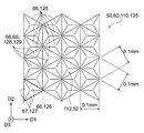
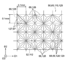
- the unit optical element When observed from the stacking direction in which the optical element portion and the light reflecting portion are laminated, the unit optical element may have dimensions smaller than a 1.5 mm square.
- the optical element portion may include a microlens having a plurality of unit optical elements.
- the unit optical element may include an element surface formed as a matte surface, and the element surface may form the uneven surface.
- the optical element portion may have a plurality of unit optical elements arranged in one direction. Each unit optical element may extend linearly in the other direction, which is not parallel to the one direction.
- the optical element portion may have a plurality of unit optical elements arranged in one direction. Each unit optical element may extend linearly in the other direction, which is non-parallel to the one direction.
- the unit optical element may be a convex portion protruding to the opposite side of the light reflecting portion.
- the optical element portion may have a plurality of unit optical elements arranged in one direction. Each unit optical element may extend linearly in the other direction, which is non-parallel to the one direction.
- the unit optical element may include an element surface having a normal direction inclined at an angle of 25 ° or less with respect to the stacking direction in which the light reflecting portion and the optical element portion are laminated.
- the optical element portion may have a plurality of unit optical elements arranged in one direction. Each unit optical element may extend linearly in the other direction, which is non-parallel to the one direction.
- the unit optical element may include a curved element surface, and the element surface may form the uneven surface.
- the optical element portion may have a plurality of unit optical elements arranged in one direction. Each unit optical element may extend linearly in the other direction, which is non-parallel to the one direction.
- the unit optical element may include an element surface formed as a matte surface, and the element surface may form the uneven surface.
- the surface light source device is with any of the first and third diffusion members according to the present disclosure described above, It includes a light source that emits light incident on the diffusion member.
- the light emitted from the light source may be P-polarized.
- the light source includes a plurality of light sources arranged regularly. At least one of the light diffusing portion and the optical element portion may include a microlens having a plurality of unit optical elements arranged in a direction non-parallel to the arrangement direction of the plurality of light sources.
- the light source includes a plurality of light sources arranged regularly. At least one of the light diffusing portion and the optical element portion includes a microlens having a plurality of unit optical elements.
- the unit optical element may include an element surface having a normal direction that is non-parallel to the arrangement direction of the plurality of light sources when observed from the stacking direction in which the light diffusing portion and the light reflecting portion are laminated. ..
- the surface light source device is A support substrate that supports the light source from the side opposite to the diffusion member is further provided.
- the diffusion member may further have a thermoplastic resin layer provided on the support substrate side of the light diffusion portion.
- the surface light source device is A support substrate that supports the light source from the side opposite to the diffusion member is further provided.
- the diffusion member may further have a thermoplastic resin layer provided on the support substrate side of the light diffusion portion.
- the display device according to the present disclosure includes any of the surface light source devices according to the present disclosure described above.
- the first dielectric multilayer film according to the present disclosure is A dielectric multilayer film used in combination with at least one of a diffractive optical element and a microlens.
- the reflectance of light of a specific wavelength incident at an incident angle of 0 ° is 80% or more, and the reflectance of at least a part of the light of the specific wavelength incident at an incident angle larger than 45 ° in absolute value is Less than 50%.
- the second dielectric multilayer film according to the present disclosure is A dielectric multilayer film used in combination with at least one of a diffractive optical element and a microlens.
- the transmittance of light of a specific wavelength incident at an incident angle of 0 ° is lower than the transmittance of light of the specific wavelength incident at an incident angle larger than 0 °.
- the method for manufacturing the first diffusion member according to the present disclosure is as follows.
- the present invention comprises a step of peeling the mold from a light diffusing portion composed of a cured product of the resin composition and laminated with the light reflecting portion.
- the method for manufacturing the second diffusion member according to the present disclosure is as follows.
- the present invention comprises a step of peeling the mold from a microlens or a diffractive optical element composed of a cured product of the resin composition and laminated with the dielectric multilayer film.
- the method for manufacturing the third diffusion member according to the present disclosure is as follows.
- the present invention comprises a step of curing a resin composition applied on the other surface of the dielectric multilayer film to form an optical element portion having an uneven surface on the dielectric multilayer film.
- the in-plane distribution of brightness can be sufficiently made uniform while reducing the thickness of the surface light source device.
- FIG. 1 is a diagram for explaining a first specific example of the embodiment, and is a perspective view showing a display device and a surface light source device.
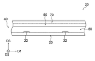
- FIG. 2 is a vertical cross-sectional view of the surface light source device of FIG.
- FIG. 3 is a plan view showing a plurality of light sources of the surface light source device of FIG.
- FIG. 4 is a graph for explaining the diffusion characteristics due to the light diffusion portion of the diffusion member that can be included in the surface light source device of FIG. 2, and shows the angular distribution of the radiation intensity.
- FIG. 5 is a perspective view showing a light diffusing portion of the diffusing member that can be included in the surface light source device of FIG. 2, and is a diagram for explaining the light diffusing characteristics of the diffractive optical element forming the light diffusing portion.
- FIG. 6 is a graph for explaining the light diffusion characteristics of the diffractive optical element of FIG. 5, and shows an angular distribution of radiant intensity.
- FIG. 7 is a vertical cross-sectional view showing an example of a microlens that can be included in the surface light source device of FIG.
- FIG. 8 is a vertical cross-sectional view showing another example of the microlens that may be included in the surface light source device of FIG.
- FIG. 9 is a vertical cross-sectional view showing still another example of the microlens that may be included in the surface light source device of FIG.
- FIG. 10 is a vertical cross-sectional view showing still another example of the microlens that may be included in the surface light source device of FIG.
- FIG. 10 is a vertical cross-sectional view showing still another example of the microlens that may be included in the surface light source device of FIG. FIG.
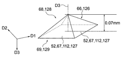
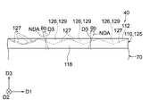
- FIG. 11A is a plan view showing an example of a specific configuration of a microlens that can be included in the surface light source device of FIG. 11B is a perspective view showing a unit optical element of the microlens of FIG. 11A.
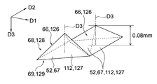
- FIG. 12A is a plan view showing another example of a specific configuration of the microlens that may be included in the surface light source device of FIG. 12B is a perspective view showing a unit optical element of the microlens of FIG. 12A.
- FIG. 13A is a plan view showing an example of a specific configuration of a microlens that can be included in the surface light source device of FIG.
- FIG. 13B is a perspective view showing a unit optical element of the microlens of FIG. 13A.
- FIG. 13A is a plan view showing an example of a specific configuration of a microlens that can be included in the surface light source device of FIG.
- FIG. 13B is a perspective view showing a unit optical element of the microlen
- FIG. 14A is a plan view showing an example of a specific configuration of a microlens that can be included in the surface light source device of FIG. 14B is a perspective view showing a unit optical element of the microlens of FIG. 14A.
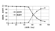
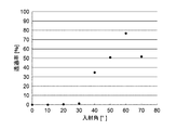
- FIG. 15 is a graph showing an example of the optical characteristics of the light reflecting portion of the diffusing member that can be included in the surface light source device of FIG. 2, and is a graph for explaining the reflection angle dependence of the reflectance and the transmittance. ..
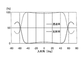
- FIG. 16 is a graph showing another example of the optical characteristics of the light reflecting portion of the diffusing member that may be included in the surface light source device of FIG.
- FIG. 17 is a graph showing still another example of the optical characteristics of the light reflecting portion that may be included in the surface light source device of FIG.
- FIG. 18 is an enlarged graph of a part of the graph of FIG.
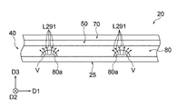
- FIG. 19 is a vertical cross-sectional view showing a surface light source device, and is a diagram for explaining the operation of the diffusion member and the surface light source device.
- FIG. 20 is a vertical cross-sectional view of the surface light source device corresponding to FIG. 2, and is a diagram for explaining the operation of the diffusion member and the surface light source device.
- FIG. 21 is a vertical cross-sectional view of the surface light source device corresponding to FIG. 2, and is a diagram for explaining the operation of the diffusion member and the surface light source device.
- FIG. 22 is a vertical cross-sectional view of the surface light source device corresponding to FIG. 2, and is a diagram for explaining the operation of the diffusion member and the surface light source device.
- FIG. 20 is a vertical cross-sectional view of the surface light source device corresponding to FIG. 2, and is a diagram for explaining the operation of the diffusion member and the surface light source device.
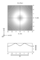
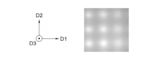
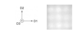
- FIG. 23A is a simulation result of calculating the in-plane distribution of the illuminance of the surface light source device according to the sample 1.
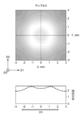
- FIG. 23B is a simulation result of calculating the in-plane distribution of the illuminance of the surface light source device according to the sample 2.
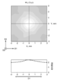
- FIG. 23C is a simulation result of calculating the in-plane distribution of the illuminance of the surface light source device according to the sample 3.
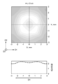
- FIG. 23D is a simulation result of calculating the in-plane distribution of the illuminance of the surface light source device according to the sample 4.
- FIG. 23E is a simulation result of calculating the in-plane distribution of the illuminance of the surface light source device according to the sample 5.
- FIG. 23B is a simulation result of calculating the in-plane distribution of the illuminance of the surface light source device according to the sample 2.
- FIG. 23C is a simulation result of calculating the in-plane distribution of the illuminance of the surface light source device according to
- FIG. 23F is a simulation result of calculating the in-plane distribution of the illuminance of the surface light source device according to the sample 6.
- FIG. 23G is a simulation result of calculating the in-plane distribution of the illuminance of the surface light source device according to the sample 7.
- FIG. 24 is a diagram for explaining a second specific example of the embodiment, and is a vertical cross-sectional view showing an example of a diffusion member that can be included in the surface light source device of FIG.
- FIG. 25A is a vertical cross-sectional view showing an example of a microlens that can be included in the optical element portion of the diffusion member of FIG. 24.
- FIG. 25B is a vertical cross-sectional view showing another example of a microlens that may be included in the optical element portion of the diffusion member of FIG. 24.
- FIG. 26 is a perspective view showing another example of the optical element portion of the diffusion member of FIG. 24.
- FIG. 27 is a vertical cross-sectional view of the optical element portion corresponding to FIG. 25A, and is a diagram for explaining the operation of the optical element portion.
- FIG. 28 is a vertical cross-sectional view of the surface light source device corresponding to FIG. 2, and is a diagram illustrating an example in which the diffusion member includes a thermoplastic resin layer.
- FIG. 29 is a vertical cross-sectional view of the surface light source device corresponding to FIG.
- FIG. 30 is a side view illustrating an example of a method of manufacturing a light diffusing portion and an optical element portion that can be included in the diffusing member of FIG. 2 or FIG. 24.
- FIG. 31 is a diagram illustrating an example of a layer structure of a light diffusing portion that can be included in the diffusing member of FIG. 2 or FIG. 24.
- FIG. 32 is a diagram illustrating another example of a method of manufacturing a light diffusing portion and an optical element portion that may be included in the diffusing member of FIG. 2 or FIG. 24.
- FIG. 30 is a side view illustrating an example of a method of manufacturing a light diffusing portion and an optical element portion that can be included in the diffusing member of FIG. 2 or FIG. 24.
- FIG. 33 is a diagram illustrating an example of a layer structure of a light diffusing portion that can be included in the diffusing member of FIG. 2 or FIG. 24.
- FIG. 34 is a diagram showing the in-plane distribution of the radiation intensity on the light emitting surface of the surface light source device according to the first embodiment.
- FIG. 35 is a diagram showing the in-plane distribution of the radiation intensity on the light emitting surface of the surface light source device according to the second embodiment.
- FIG. 36 is a diagram showing the in-plane distribution of the radiation intensity on the light emitting surface of the surface light source device according to the third embodiment.
- FIG. 37 is a diagram showing the in-plane distribution of the radiation intensity on the light emitting surface of the surface light source device according to the fourth embodiment.
- FIG. 34 is a diagram showing the in-plane distribution of the radiation intensity on the light emitting surface of the surface light source device according to the first embodiment.
- FIG. 35 is a diagram showing the in-plane distribution of the radiation intensity on the light
- FIG. 38 is a diagram showing the in-plane distribution of the radiation intensity on the light emitting surface of the surface light source device according to the fifth embodiment.
- FIG. 39 is a diagram showing the in-plane distribution of the radiation intensity on the light emitting surface of the surface light source device according to the sixth embodiment.
- FIG. 40 is a diagram showing the in-plane distribution of the radiation intensity on the light emitting surface of the surface light source device according to Comparative Example 1.
- sheet is not distinguished from each other based only on the difference in designation.
- sheet is a concept that includes members that can be called “film” or “board”, and is not distinguished only by the difference in name.
- the normal direction of the sheet-shaped (sheet-shaped, plate-shaped) member refers to the normal direction of the target sheet-shaped (film-shaped, plate-shaped) member to the sheet surface.
- the "sheet surface (film surface, plate surface)” is a target sheet-like member (film-like) when the target sheet-like (film-like, plate-like) member is observed as a whole and from a broad perspective. Refers to a surface that coincides with the plane direction of the member (member, plate-shaped member).
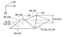
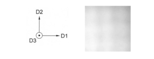
- the first direction D1, the second direction D2, and the stacking direction D3 are indicated by arrows as common directions between the drawings.
- the tip side of the arrow is one side of each direction D1, D2, D3.
- an arrow directed toward the back of the paper along the direction perpendicular to the paper of the drawing is indicated by a symbol with an X in the circle.
- an arrow pointing from the paper surface to the front along the direction perpendicular to the paper surface of the drawing is indicated by a symbol having dots in the circle.
- FIG. 1 is a perspective view schematically showing a display device 10 as an application example of the surface light source device 20 and the diffusion member 40.
- the display device 10 displays, for example, a moving image, a still image, character information, or an image composed of a combination thereof.
- the display device 10 can be used, for example, as an in-vehicle liquid crystal display device.
- the display device 10 can be used indoors or outdoors for various purposes such as advertising, presentations, television images, and display of various information.
- the display device 10 shown in FIG. 1 has a surface light source device 20 having a light emitting surface 20a and a display panel 15 arranged so as to face the light emitting surface 20a.
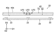
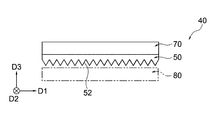
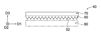
- FIG. 2 is a vertical cross-sectional view showing a surface light source device 20 as a first specific example.
- the surface light source device 20 has a light source 22 and a diffusion member 40 that adjusts the optical path of the light emitted from the light source 22 as main components.
- the diffusion member 40 is arranged so as to face the light source 22. That is, the diffusion member 40 is a sheet-like member and faces the light source 22 in the normal direction thereof.
- the diffusing member 40 can effectively eliminate the unevenness of brightness caused by the presence of the light source 22 by diffusing the light emitted from the light source 22.
- the illuminance at each position on the light emitting side surface 40b of the diffusion member 40 or the illuminance at each position on the virtual light receiving surface parallel to the light emitting side surface 40b located near the light emitting side surface 40b can be made uniform.
- the diffusion member 40 described in the present embodiment is devised to sufficiently make the in-plane distribution of brightness uniform while reducing the thickness of the surface light source device 20.
- the “illuminance on the light emitting side surface 40b” used in the following description means “illuminance on the light emitting side surface 40b” or “illuminance on the light receiving surface” described above.
- the display device 10 the surface light source device 20, and the diffusion member 40 in one embodiment will be described with reference to the illustrated first specific example.
- the display panel 15 of the display device 10 will be described. As shown in FIG. 1, the display panel 15 is laminated with the surface light source device 20 in the stacking direction D3. The display panel 15 is arranged so as to face the light emitting surface 20a of the surface light source device 20. The display panel 15 has a display surface 15a on which an image is displayed as a surface facing the side opposite to the surface light source device 20 in the stacking direction D3. In the illustrated example, the display panel 15 is formed in a rectangular shape when observed from the stacking direction D3, that is, in a plan view from the front direction.
- the display panel 15 is configured as, for example, a transmissive liquid crystal display panel. A part of the light incident from the surface light source device 20 is transmitted through the display panel 15 as a liquid crystal display panel, so that an image is displayed on the display surface 15a.
- the display panel 15 includes a liquid crystal layer having a liquid crystal material. The light transmittance of the display panel 15 changes according to the strength of the electric field applied to the liquid crystal layer.
- a liquid crystal display panel having a pair of polarizing plates and a liquid crystal cell (liquid crystal layer) arranged between the pair of polarizing plates can be used.
- the polarizing plate has a polarizer.
- the polarizer decomposes the incident light into two vertical polarization components.
- the polarization component in one direction passes through the polarizer.
- the polarization component in the other direction which is perpendicular to one direction, is absorbed by the polarizer.
- the liquid crystal cell has a pair of support plates and a liquid crystal display arranged between the pair of support plates. The liquid crystal cell is configured so that an electric field can be applied to each region forming one pixel.
- the orientation of the liquid crystal in the liquid crystal cell to which an electric field is applied changes.
- the polarized light component in a specific direction emitted from the surface light source device 20 and transmitted through the polarizing plate arranged on the surface light source device 20 side of the liquid crystal cell is polarized when passing through the liquid crystal cell to which no electric field is applied. Rotate the direction 90 °.
- the polarization component in a specific direction maintains its polarization direction when passing through a liquid crystal cell to which an electric field is applied.
- Whether the polarization component in a specific direction that has passed through one polarizing plate is further transmitted through the other polarizing plate or is absorbed by the other polarizing plate and blocked is controlled by the presence or absence of an electric field applied to the liquid crystal cell. can.
- the surface light source device 20 has a light emitting surface 20a that emits planar light.
- the surface light source device 20 is configured as a direct type backlight.
- the light source 22 is provided in the region overlapping the light emitting surface 20a.
- the normal direction of the display panel 15, the normal direction of the display surface 15a, the normal direction of the light emitting surface 20a, the normal direction of the diffusion member 40, and the light diffusion portion 50 included in the diffusion member 40 which will be described later.
- the normal directions of the light reflecting portion 70 and the optical element portion 110, and the normal directions of the support substrate 25 described later that supports the light source 22 are parallel to each other. In the illustrated example, these normal directions coincide with the stacking direction D3 and are also referred to as the front direction.
- the light source 22 has a light emitting element that emits light.
- a light emitting diode is exemplified as a light emitting element.
- the light emitting diode is also referred to as an LED.
- the dimensions of the light emitting diode used as the light source 22 are not particularly limited. From the viewpoint of making the image of the light source 22 inconspicuous, a small light emitting diode, for example, a mini LED or a micro LED may be used.
- the lengths WL1 and WL2 on one side of the light source 22 having a quadrangular shape in the observation from the stacking direction D3 shown in FIG. 3 may be preferably 0.5 mm or less, more preferably 0.2 mm or less. But it may be.
- the emission wavelength of the light source 22 can be appropriately selected according to the application of the surface light source device 20.
- the surface light source device 20 may have a light emitting element that emits blue light and a light emitting element that emits yellow light, and may generate white light.
- the surface light source device 20 may include a light emitting element that emits blue light, a light emitting element that emits green light, and a light emitting element that emits red light, and may generate white light.
- one light source 22 may include a plurality of types of light emitting elements arranged close to each other, or may include only a single light emitting element. That is, a plurality of types of light sources 22 having different emission wavelengths may be used.
- the light source 22 may include a light emitting diode that emits blue light having a wavelength of 450 nm as a light emitting element.
- a light emitting diode having a large output can be used as the light source 22.
- the light source 22 may be composed of only a light emitting element.
- the light source 22 may include an optical element such as a cover or a lens that adjusts the light distribution from the light emitting element in addition to the light emitting element, or absorbs the light from the light emitting element to emit light having a different wavelength. It may contain an emitting phosphor.
- the light distribution characteristics of the light source 22 are not particularly limited.
- the light distribution characteristic of the light source 22 may be a Lambertian light distribution. With the Lambertian light distribution, the highest peak intensity is obtained in the stacking direction D3, which is the optical axis, in the emission intensity distribution from the light source 22 directed to the stacking direction D3, and the peak is obtained in a direction inclined by 60 ° from the optical axis. Half the strength is obtained.
- the peak intensity may be obtained in a direction other than the stacking direction D3.
- the bad wing light distribution disclosed in Patent Document 1 JP6299811B
- Patent Document 1 JP6299811B
- the surface light source device 20 may have a plurality of light sources 22 or may have only a single light source 22.
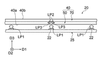
- the quantity of the light source 22 is appropriately selected according to the application of the surface light source device 20, the area of the light emitting surface 20a, and the like. From the viewpoint of eliminating the unevenness of brightness caused by the arrangement of the light sources 22, it is preferable that the plurality of light sources 22 included in the surface light source device 20 are regularly arranged on the surface perpendicular to the stacking direction D3.
- a plurality of light sources 22 are arranged in a honeycomb array arranged at a constant pitch in each of three directions inclined by 60 ° with each other, or in a square array arranged at a constant pitch in each of two directions perpendicular to each other. May be arranged.
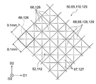
- the plurality of light sources 22 are arranged at a constant pitch in each of the first direction D1 and the second direction D2 perpendicular to each other.
- the array pitch PL1 in the first direction D1 and the light distribution pitch PL2 of the light source 22 in the second direction D2 are the same.
- the example is not limited to the illustrated example, and the array pitch PL1 and the array pitch PL2 may be different.
- the first direction D1 and the second direction D2 are parallel to the side edges of the rectangular surface light source device 20 and the diffusion member 40, respectively.
- the array pitch PL1 and the array pitch PL2 of the light source 22 may be 0.2 mm or more and 10 mm or less, respectively.
- the light source 22 may emit only P-polarized light when it enters the diffusion member 40.
- the P-polarized light is light that vibrates on a surface including the traveling direction of the light when it is incident on the diffusing member 40 and the normal direction of the diffusing member 40 to the incoming light side surface 40a.
- the illustrated surface light source device 20 further has a support substrate 25 that supports the light source 22 in addition to the light source 22 and the diffusion member 40.
- the support substrate 25 supports a plurality of light sources 22 from the side opposite to the diffusion member 40 in the stacking direction D3.
- the support substrate 25 includes a circuit that supplies electric power to the light source 22.
- the support substrate 25 is a sheet-like member.
- the support substrate 25 has a light reflectivity that reflects light and directs it toward the diffusion member 40.
- the light reflectivity of the support substrate 25 is not particularly limited as long as it is exhibited with respect to the light emitted from the light source 22 or the light used for light emission by the surface light source device 20.
- the light used for light emission in the surface light source device 20 may include light emitted from the light source 22 and wavelength-converted.
- the sheet-shaped substrate main body 26, the reflective layer 27 laminated on the substrate main body 26 from the diffusion member 40 side in the stacking direction D3, and the light source 22 are electrically connected. It has a wiring 28 and.
- the substrate body 26 extends in a direction perpendicular to the stacking direction D3, and the substrate body 26 has an insulating property.
- the reflective layer 27 is reflective to the light emitted from the light source 22 or to the light used for light emission by the surface light source device 20.
- the reflectivity of the reflective layer 27 may be regular reflection, which is also called specular reflection, diffuse reflection, or anisotropic diffuse reflection.
- the substrate body 26 may be a resin film containing diffusion particles, for example, a film made of white polyethylene terephthalate.
- the reflective layer 27 may be a metal layer laminated on the substrate main body 26, or may be a reflective diffractive optical element.
- the wiring 28 is electrically connected to a terminal (not shown) of the light source 22 via solder or the like. When the substrate body 26 and the reflective layer 27 have an insulating property, the wiring 28 is preferably located between the substrate body 26 and the reflective layer 27.
- the light source 22 may be covered with the sealing material 23.
- the sealing material 23 is provided corresponding to each light source 22.
- the encapsulant 23 is two-dimensionally arranged in the same manner as the light source 22.
- the light source 22 has a surface and a side surface facing the diffusion member 40 covered with a sealing material 23.
- the sealing material 23 is fixed to the support substrate 25.
- the portion where the light source 22 and the wiring 28 are electrically connected may also be covered with the sealing material 23.
- a thermosetting resin such as a silicone resin or an epoxy resin
- a thermoplastic resin such as an olefin resin
- the diffusion member 40 is arranged on the sealing material 23. That is, the diffusion member 40 is supported by the sealing material 23 and is separated from the light source 22 and the support substrate 25 in the stacking direction D3.
- the sealing material 23 may be bonded to the diffusion member 40 by adhesion, adhesion, welding or the like.
- the distance DX shown in FIG. 2 is the distance between the light source 22 and the diffusion member 40 along the stacking direction D3. In other words, the distance DX refers to the distance along the stacking direction D3 between the surface of the light source 22 facing the diffusion member 40 side and the light incoming side surface 40a of the diffusion member 40.
- the diffusion member 40 has a light diffusion unit 50 and a light reflection unit 70 in this order.
- the light diffusing unit 50 is located on the light input side of the light to be diffused by the diffusing member 40 with the light reflecting unit 70 as a reference.
- the light reflecting unit 70 is located on the light emitting side of the light to be diffused by the diffusing member 40 with the light diffusing unit 50 as a reference.
- the diffusion member 40 has a sheet shape.
- the diffusion member 40 extends in the first direction D1 and the second direction D2 perpendicular to the stacking direction D3.
- the light diffusing portion 50 forms the light entering side surface 40a of the diffusing member 40.
- the light reflecting portion 70 forms the light emitting side surface 40b of the diffusion member 40.
- the light diffusing portion 50 and the light reflecting portion 70 may be joined to each other, may be merely in contact with each other and may not be joined to each other, and may be separated from each other. ..
- the light diffusing unit 50 has light transmissivity and light diffusing property with respect to the light emitted from the light source 22 or the light used for light emission by the surface light source device 20.
- the light diffusing unit 50 has light transmissivity and light diffusing property with respect to visible light.
- the light diffusing portion 50 may include an optical sheet 55 that is simply overlapped with another member or bonded to another member by adhesion or adhesion, may be an optical sheet 55, or may be an optical sheet 55, a member, a structure, or the like. It may be a part, or may be a surface of an optical sheet, a member, a structure, or the like.
- the total light transmittance of the light diffusing unit 50 is preferably 50% or more, more preferably 70% or more, and further preferably 90% or more.
- the utilization efficiency of the light from the light source 22 is improved.
- the light diffusing unit 50 is applied to the surface light source device 20, the in-plane distribution of the illuminance on the light emitting side surface 40b of the diffusing member 40 can be effectively made uniform. Therefore, the light diffusing unit 50 is made of a material having high transparency to the light emitted from the light source 22 or to the light used for light emission by the surface light source device 20.
- the total light transmittance is a value measured by a method based on JIS K7361-1: 1997, with the incident angle set to 0 degree.
- the total light transmittance is a value measured using an ultraviolet-visible near-infrared spectrophotometer V-7200 manufactured by JASCO Corporation.
- the light diffusivity of the light diffusing unit 50 may be isotropic diffusion or anisotropic diffusion.
- the light diffusing unit 50 may diffuse light in a direction within a specific angle range.
- the specific angle range may be one, or may be plural apart from each other.
- the diffusion by the light diffusing unit 50 is not limited to diffusing the transmitted light, and the reflected light may be diffused.
- the diffusion angle ⁇ of the light incident on the light diffusing unit 50 is preferably 10 ° or more, more preferably 15 ° or more, and further preferably 20 ° or more.
- the diffusion angle of the light incident on the light diffusion unit 50 is preferably 85 ° or less, more preferably 60 ° or less, and even more preferably 50 ° or less.
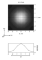
- the diffusion angle ⁇ is the half-value full width (FWHM) in the angular distribution of the radiant intensity (watt / steradian) obtained when light is incident on the light entry side surface of the light diffusion unit 50 at an incident angle of 0 °. ..
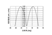
- FIG. 4 is a graph showing an angular distribution of radiation intensity on the light emitting side surface of the light diffusing portion 50 when a parallel light flux is incident on the incident side surface of the light diffusing portion 50 at an incident angle of 0 °.
- the vertical axis is the value of radiant intensity
- the horizontal axis is the emission angle.
- the half-value full width in the angular distribution of radiant intensity corresponding to each diffusion ⁇ is the width (°) of the range of the emission angle at which half of the maximum transmitted light intensity I max in the angular distribution of radiant intensity can be obtained.
- the angular distribution of radiant intensity can be measured using a variable angle photometer or a variable angle spectrophotometer.
- a variable angle photometer (goniophotometer) GP-200 manufactured by Murakami Color Technology Research Institute can be used.
- the incident angle means the angle (°) formed by the traveling direction of the incident light with respect to the normal direction of the sheet-like member to which the light is incident.
- the emission angle means an angle (°) formed by the traveling direction of the emitted light with respect to the normal direction of a member such as a sheet from which the light is emitted.
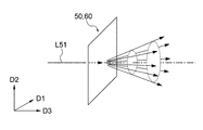
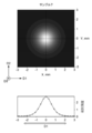
- FIG. 5 is a perspective view for explaining another preferable light diffusing characteristic of the light diffusing portion 50, which has a light diffusing property different from that of FIG.
- the light ray L51 is incident on the light diffusing portion 50 at an incident angle of 0 °. That is, the light ray L51 is vertically incident on the light diffusing portion 50.
- the light ray L51 is diffused by optical actions such as refraction, reflection, and diffraction in the light diffusing portion 50. According to the light diffusing portion 50 shown in FIG.
- the light ray L51 is mainly a circle from the apex to the bottom surface of a cone whose apex is located on the light diffusing portion 50 and whose bottom surface is arranged parallel to the light diffusing portion 50. It is traveling along the optical path toward each position on the circumference.
- the radiant intensity on the side of the light diffusing portion 50 facing the light reflecting portion 70 has a peak at an emission angle other than 0 °. ..
- the radiation intensity on the side of the light diffusing portion 50 facing the light reflecting portion 70 is the emission direction in which the emission angle is 0 °. It has a peak at an emission angle other than 0 ° in the angle distribution in any plane including.
- the absolute value of the emission angle having a peak of radiant intensity may be preferably 30 ° or more and 60 ° or less, more preferably 30 ° or more and 50 ° or less, and further preferably 30 ° or more and 45 ° or less.
- the absolute value of the emission angle of 90% or more of the light incident on the light diffusing unit 50 at an incident angle of 0 ° may be 30 ° or more and 60 ° or less.
- the absolute value of the emission angle of 95% or more of the light incident on the light diffusing unit 50 at an incident angle of 0 ° may be 30 ° or more and 60 ° or less.
- the absolute value of the emission angle of 98% or more of the light may be 30 ° or more and 60 ° or less.
- the diffusing member 40 suppresses the illuminance in the region directly above the light source 22 from becoming too high, and is perpendicular to the stacking direction D3.
- the illuminance in the region separated from the light source 22 in the above direction can be increased.
- the in-plane distribution of illuminance can be effectively made uniform.
- the reflectance of the light incident on the light reflecting unit 70 which will be described later, at an incident angle of 0 ° or more and a peak angle or less in absolute value is preferable. It is 80% or more. It is more preferably 85% or more, and further preferably 90% or more.
- the peak angle means an absolute value of an emission angle having a peak of radiant intensity.
- the solid line in FIG. 6 is a graph showing the angular distribution of the radiation intensity on the light emitting side surface of the light diffusing portion 50 shown in FIG. 5 when the incident angle of the incident light is 0 °.
- the light diffusing unit 50 is not particularly limited, and various configurations having light transmissivity and light diffusing property can be adopted.
- the light diffusing unit 50 may include at least one of a transmissive diffractive optical element 60 and a microlens 65.
- the diffractive optical element 60 is an element that exerts a diffractive action on incident light.
- the diffractive optical element 60 may be a hologram element.
- a diffractive optical element having diffractive properties for achieving the desired light diffusivity can be designed relatively easily.
- the diffractive optical element 60 may have the diffusion characteristics shown in FIG.
- the microlens 65 has a plurality of unit optical elements 66.
- the unit optical element 66 is an element that changes the traveling direction of light by refraction, reflection, or the like.
- the unit optical element 66 is a concept including an element called a unit shape element, a unit prism, and a unit lens.
- the unit optical element 66 is configured as a convex portion 68 or a concave portion 69.
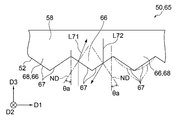
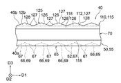
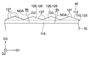
- the light diffusing portion 50 has a main body portion 58, and a unit optical element 66 as a convex portion 68 is formed in the main body portion 58.
- the light diffusing portion 50 may have a main body portion 58 and a unit optical element 66 as a recess 69 provided on the main body portion 58.
- the main body 58 has a sheet shape.
- the main body 58 extends in the first direction D1 and the second direction D2 perpendicular to the stacking direction D3. In the example shown in FIG. 2, the main body portion 58 is joined to the light reflecting portion 70.
- the unit optical element 66 has an element surface 67 inclined with respect to the stacking direction D3.
- the unit optical element 66 is defined by the element surface 67.
- the microlens 65 has an uneven surface 52 formed by the element surface 67 of the unit optical element 66.
- the microlens 65 can bend the traveling direction of the incident light by the uneven surface 52.
- the uneven surface 52 may face either direction in the stacking direction D3.
- the uneven surface 52 faces the light source 22 in the stacking direction D3.
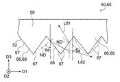
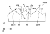
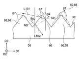
- the uneven surface 52 faces the light reflecting portion 70 in the stacking direction D3.
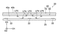
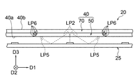
- the uneven surface 52 can bend the traveling direction of the light L71, L81, L91, L101 incident from the light source 22 side, and can change the traveling direction of the light L72, L82, L92, L102 incident from the light reflecting portion 70 side. Can be bent. In particular, as shown in FIGS.
- the microlens 65 bends the traveling direction of the incident light from a direction having a small inclination angle with respect to the stacking direction D3, and makes the inclination angle with respect to the stacking direction D3 larger than that at the time of incident. Can be done. That is, the inclination angle formed by the traveling direction of the light emitted from the light diffusing portion 50 with respect to the stacking direction D3 is made larger than the inclination angle formed by the traveling direction of the incident light to the light diffusing portion 50 with respect to the stacking direction D3. be able to.
- the traveling direction of the light is changed by refracting the lights L71, L72, L91, and L92 at the element surface 67.
- the traveling direction of the light is changed by reflecting the lights L82 and L101 on the element surface 67, preferably by total internal reflection.
- the change in the traveling direction due to the reflection shown in FIGS. 8 and 10 tends to be larger than the change in the traveling direction due to the refraction shown in FIGS. 7 and 9.
- the more the normal direction ND of the element surface 67 is inclined with respect to the stacking direction D3, in other words, the more the element surface 67 rises in the stacking direction D3, the more easily the light is reflected by the element surface 67.
- the normal direction ND of the element surface 67 forms an inclination angle ⁇ a larger than 45 ° with respect to the stacking direction D3
- the light not significantly inclined with respect to the stacking direction D3 is the element surface 67.
- the traveling direction of the light is greatly inclined with respect to the stacking direction D3 due to the reflection at.
- the unit optical element 66 may include an element surface 67 having a normal direction ND inclined at an inclination angle ⁇ a larger than 45 ° with respect to the stacking direction D3. .. Since the element surface 67 rises in the stacking direction D3, reflection, preferably total reflection, is likely to occur. That is, according to the unit optical element 66 including the element surface 67, the optical path of the light transmitted through the microlens 65 can be greatly bent by reflection, preferably by total reflection. By greatly adjusting the traveling direction of light, the in-plane distribution of illuminance can be more effectively homogenized.
- the diffusion characteristic of the microlens 65 is affected by the tilt angle ⁇ a of the element surface 67 of the unit optical element 66. Therefore, the cross-sectional shape of the microlens 65 can be appropriately adjusted based on the optical characteristics required for the surface light source device 20 and the diffusion member 40.
- the inclination angles ⁇ a of the plurality of element surfaces 67 included in one unit optical element 66 may be different from each other or may be the same.
- the plurality of unit optical elements 66 included in the microlens 65 may be different from each other in the configuration such as shape, orientation, and size.
- a plurality of unit optical elements 66 included in the microlens 65 may have the same configuration as each other.
- the inclination angle ⁇ a is preferably 25 ° or less, more preferably 20 ° or less, still more preferably 15 °. It is as follows.
- the element surface 67 may be slightly curved.
- the unit optical element 66 may have an outer shape of a part of a sphere such as a hemisphere, or may have an outer shape of a part of a spheroid.
- the optical path of the light transmitted through the microlens 65 is bent in various directions due to reflection or refraction.
- the in-plane distribution of illuminance can be more effectively made uniform.
- the change in the angular distribution of radiant intensity can be effectively smoothed.
- the unit optical element 66 may include an element surface 67 formed as a matte surface.
- the element surface 67 as a matte surface scatters light in various directions.
- the in-plane distribution of illuminance can be more effectively made uniform.
- the change in the angular distribution of radiant intensity can be effectively smoothed.
- the plurality of unit optical elements 66 included in the microlens 65 are two-dimensionally arranged. Therefore, the element surface 67 of the unit optical element 66 included in the microlens 65 faces in various directions. As a result, the microlens 65 can guide light in various directions by the two-dimensionally arranged unit optical elements 66.
- the plurality of unit optical elements 66 may be arranged irregularly or may be arranged regularly. By regularly arranging the plurality of unit optical elements 66, the design of the microlens 65 becomes easy, and the unit optical elements 66 can be easily spread without gaps.
- microlens 65 a plurality of specific examples of the microlens 65 will be described with reference to FIGS. 11A to 14B.
- the microlens 65 shown in these figures was the subject of the simulation described later.
- the arrangement of the plurality of unit optical elements 66 is a square arrangement.
- the plurality of unit optical elements 66 are arranged in the first direction D1 at a constant pitch.
- the plurality of unit optical elements 66 are also arranged at a constant pitch in the second direction D2.
- the arrangement pitch in the first direction D1 and the arrangement pitch in the second direction D2 may be the same or different.
- the arrangement pitch in the first direction D1 and the arrangement pitch in the second direction D2 are the same as each other and are 0.1 mm.
- each unit optical element 66 has a shape in which the bottom of the cone is cut off from all sides.
- the cone is arranged at a placement pitch shorter than the diameter of the bottom surface of the cone shown by the dotted line in FIG. 11A, and the portion where the adjacent cones overlap in the first direction D1 and the second direction D2 is cut off to form the microlens 65. It has been made.
- the plurality of unit optical elements 66 are spread without gaps.
- the height of each unit optical element 66 in the stacking direction D3 is 0.09 mm as an example.
- the illustrated unit optical element 66 has an element surface 67 that corresponds to the side surface of the cone.
- Each unit optical element 66 can diffuse light radially when observed from the stacking direction D3.
- the arrangement of the plurality of unit optical elements 66 is a square arrangement.
- the plurality of unit optical elements 66 are arranged at a constant pitch in two directions inclined by ⁇ 45 ° with respect to the first direction D1.
- the arrangement pitch in each direction may be the same or different.
- the arrangement pitches of the unit optical elements 66 in the two directions are the same as each other and are 0.1 mm.
- the unit optical element 66 has a quadrangular pyramid shape having a square bottom surface.
- the height of each unit optical element 66 in the stacking direction D3 is 0.07 mm as an example.
- the microlens 65 has two types of unit optical elements 66.
- the unit optical elements 66 of each type are arranged at a constant pitch in the second direction D2 and two directions inclined by ⁇ 60 ° with respect to the second direction. That is, the two types of unit optical elements 66 are arranged at a constant pitch in each of the three directions inclined by 60 ° with respect to each other.
- the array of unit optical elements 66 shown is also referred to as a honeycomb array.
- the arrangement pitch in each direction may be the same or different. In the illustrated example, the arrangement pitches of the unit optical elements 66 in the three directions are the same as each other.
- the shapes of the bottom surfaces of the two types of unit optical elements 66 are the same.
- the shape of the bottom is an equilateral triangle.
- the orientation of the bottom surface of the two types of unit optical elements 66 is different. When one unit optical element 66 is rotated by 60 °, the orientation of the bottom surface of one unit optical element 66 coincides with the orientation of the bottom surface of the other unit optical element 66.
- the unit optical element 66 has the shape of a triangular pyramid whose bottom surface is an equilateral triangle.
- the height of the bottom surface of the unit optical element 66 is 0.1 mm as an example.
- the height of the unit optical element 66 is 0.08 mm as an example.
- Each unit optical element 66 may have a regular triangular pyramid shape.
- the unit optical elements 66 having the same bottom surface are arranged in four directions.
- the plurality of unit optical elements 66 having the same shape and orientation of the bottom surface are arranged at a constant pitch in each of the first direction D1 and the second direction D2.
- the arrangement pitches in the two directions may be the same or different.
- the arrangement pitch in each of the two directions is the same.
- the unit optical element 66 has a triangular pyramid shape whose bottom surface is a right-angled isosceles triangle shape.
- the length of the equilateral sides of the right-angled isosceles triangle forming the bottom surface is 0.1 mm as an example.
- the height of the unit optical element 66 is 0.01 mm as an example.
- the perpendicular line from the apex to the bottom surface of the cone forming the unit optical element 66 may pass through the center of gravity of the bottom surface.
- the unit optical element 66 projects toward the light source 22 in the stacking direction D3. That is, the unit optical element 66 is a convex portion 68 protruding from the main body portion 58.
- the unit optical element 66 may be a recess 69 formed in the main body 58.
- the maximum length of the unit optical element 66 in the direction perpendicular to the stacking direction D3 is preferably 1.5 mm or less, more preferably 1 mm or less, still more preferably 0.5 mm. It is as follows.
- one unit optical element 66 may have a dimension smaller than the dimension obtained by triple the light source 22 in each of the two directions perpendicular to each other when observed from the stacking direction D3. preferable.
- the lengths WL1 and WL2 of one side of the light source 22 having a quadrangular shape in the observation from the stacking direction D3 shown in FIG. 3 are preferably 0.5 mm or less, more preferably 0.2 mm or less.
- the unit optical element 66 preferably has a dimension smaller than a 1.5 mm square, and more preferably a dimension smaller than a 0.6 mm square.
- one dimension is smaller than the other dimension, it means that one outer contour is located on the other outer contour or inside the other outer contour in at least one direction. ..
- the dimension of the unit optical element 66 along an arbitrary direction may be three times or less the dimension of the light source 22 along the direction.
- the light emitted from the diffusing member 40 using these unit optical elements 66 is constant without depending on the relative position between the diffusing member 40 and the light source 22 along the directions D1 and D2 perpendicular to the stacking direction D3. It comes to have light distribution characteristics. That is, the surface light source device 20 can be assembled without positioning the diffusion member 40 and the light source 22 along the directions D1 and D2 perpendicular to the stacking direction D3. That is, the diffusion member 40 can be arranged on the light source 22 by alignment-free.
- the arrangement pitch of the unit optical elements 66 having such dimensions may be 0.01 mm or more and 1.5 mm or less.
- the arrangement pitch of the unit optical elements 66 is preferably 0.05 mm or more and 1 mm. It is less than or equal to, more preferably 0.1 mm or more and 0.5 mm or less.
- the microlens 65 is observed from the stacking direction D3 in the normal direction ND to the element surface 67. Diffuses light. In other words, the microlens 65 guides light in the normal direction ND of the element surface 67 observed from the stacking direction D3.
- the arrangement interval of the plurality of light sources 22 becomes shorter along the arrangement direction of the light sources 22, but becomes longer in a direction non-parallel to the arrangement direction of the light sources 22.
- the unit optical element 66 has a normal direction ND that is non-parallel to the arrangement direction of the plurality of light sources 22 when observed from the stacking direction D3. Includes surface 67. More preferably, the unit optical element 66 has a normal direction ND inclined at an angle of 35 ° or more and 55 ° or less with respect to the arrangement direction of the plurality of light sources 22 in the observation from the stacking direction D3, and the element surface 67 is formed. Includes. According to such an arrangement, light can be effectively diffused in a direction non-parallel to the arrangement direction of the plurality of light sources 22 by reflection or refraction at the unit optical element 66. As a result, the in-plane distribution of illuminance can be more effectively made uniform.
- the unit optical element 66 has four element surfaces 67.
- the normal direction NDs of the four element surfaces 67 are all inclined by 45 ° with respect to the first direction D1 and the second direction D2, which are the arrangement directions of the light sources 22.
- the position CP at the center of the four adjacent light sources 22 tends to be the darkest.
- the four light sources 22 include two light sources 22A adjacent to one arrangement direction D1 and two other light sources 22B adjacent to the two light sources 22A from one side in the other arrangement direction D2, respectively. ..
- light can be efficiently guided towards this darkest position CP, effectively uniformizing the in-plane distribution of illuminance.
- the diffusion member 40 may be provided with a display 42 (see FIG. 1) indicating the direction in which the diffusion member 40 should be arranged.
- the display 42 functions as a so-called alignment mark.
- the display 42 provided on the diffusion member 40 may display the direction of the element surface 67 in the normal direction ND.
- the display 42 may indicate a preferred direction in which the diffusion member 40 should be arranged with respect to the light source 22 or the support substrate 25.
- the display 42 may display a preferred arrangement direction of the light sources 22 with respect to the diffusion member 40.
- a display related to the arrangement direction of the light source 22 is provided on the support substrate 25, and the diffusion member 40 is positioned in an appropriate direction with respect to the arrangement of the light source 22 based on the display of the support substrate 25 and the display 42 of the diffusion member 40. You may.
- the light diffusing unit 50 may include a microlens 65 having a plurality of unit optical elements 66 arranged in a direction non-parallel to the arrangement direction of the plurality of light sources 22. That is, the arrangement direction of the plurality of unit optical elements 66 may be non-parallel to the arrangement direction of the plurality of light sources 22. According to such an arrangement, moire caused by the superposition of the arrangement of the unit optical elements 66 and the arrangement of the light source 22 can be effectively made inconspicuous.
- the diffractive optical element 60 and the microlens 65 that can be used in the light diffusing unit 50 have been described.
- the diffractive optical element 60 and the microlens 65 are merely examples, and other elements having both light transmission and light diffusivity may be used as the light diffusing unit 50.
- the above-mentioned elements having specific properties of light transmission and light diffusivity may be preferably used as the light diffusing unit 50.
- an optical sheet or the like having a light transmitting base material and light diffusing particles dispersed in the base material may be used as the light diffusing unit 50.
- the light reflecting portion 70 is located on the opposite side of the light diffusing portion 50 from the light source 22 in the stacking direction D3.
- the light reflecting unit 70 has a light reflecting property that reflects visible light. The reflectance and transmittance of the light reflecting unit 70 change depending on the incident angle.
- the transmittance of the light of a specific wavelength incident at an incident angle of 0 ° at the light reflecting unit 70 is larger than the transmittance of the light of a specific wavelength incident at an incident angle larger than 0 ° at the light reflecting unit 70. small. That is, the transmittance of the vertically incident specific wavelength light in the light reflecting unit 70 is smaller than the transmittance of the light reflecting unit 70 of the specific wavelength light incident from at least one oblique direction.
- the reflectance of the light of a specific wavelength incident at an incident angle of 0 ° at the light reflecting unit 70 is larger than the reflectance of the light of a specific wavelength incident at an incident angle larger than 0 ° at the light reflecting unit 70. big.
- the light reflecting unit 70 can also be described as a selective light reflecting unit, a light transmitting unit, and a selective light transmitting unit.
- the light reflecting unit 70 reflects light of a specific wavelength incident at an incident angle of 0 ° with a reflectance of 80% or more.
- the light reflecting unit 70 transmits light of a specific wavelength incident at an incident angle of 0 ° with a transmittance of less than 20%. Further, the light reflecting unit 70 reflects light of at least a part of a specific wavelength incident at an incident angle larger than 45 ° in absolute value with a reflectance lower than 50%.
- the light reflecting unit 70 transmits light of at least a part of a specific wavelength incident at an incident angle larger than 45 ° in absolute value with a transmittance of 50% or more.
- the light reflecting unit 70 has an incident angle dependence of the reflectance. Further, the light reflecting unit 70 has an incident angle dependence of the transmittance.
- FIG. 15 is a graph showing an example of reflection characteristics and transmission characteristics according to the incident angle of the light reflecting unit 70.
- the reflectance of light of a specific wavelength having an incident angle of 70 ° or more and less than 90 ° in absolute value at the light reflecting portion 70 may be less than 70%, less than 60%, or less than 50%.
- the reflectance of light of a specific wavelength having an incident angle of 60 ° or less in the light reflecting portion 70 may be 50% or more and less than 100%, 80% or more and less than 100%, and 90% or more and less than 100%. It's fine.
- the reflectance of light of a specific wavelength having an incident angle of 0 ° at the light reflecting portion 70 may be 80% or more and less than 100%, 90% or more and less than 100%, or 95% or more and less than 100%.
- the transmittance of light of a specific wavelength in the light reflecting unit 70 decreases.
- the transmittance of light having a specific wavelength having an incident angle of 70 ° or more and less than 90 ° in the light reflecting portion 70 may be 30% or more, 40% or more, or 50% or more.
- the transmittance of light of a specific wavelength having an incident angle of 60 ° or less in the light reflecting portion 70 may be 0% or more and less than 50%, 0% or more and less than 20%, and 0% or more and less than 10%. But it may be.
- the transmittance of light of a specific wavelength having an incident angle of 0 ° at the light reflecting portion 70 may be 0% or more and less than 20%, 0% or more and less than 10%, or 0% or more and less than 5%.
- the light of a specific wavelength can be appropriately set according to the application of the surface light source device 20 and the diffusion member 40.
- the light emitted from the light source 22 or the light used for light emission by the surface light source device 20 may be light having a specific wavelength.
- Light of a specific wavelength may be visible light.
- "Visible light” means light having a wavelength of 380 nm or more and a wavelength of 780 nm or less.
- the reflectance of the light reflecting portion shall be a value measured using a variable angle photometer (goniophotometer) GP-200 manufactured by Murakami Color Technology Research Institute.
- the transmittance of the light reflecting portion is the total light transmittance measured in accordance with JIS K7361-1: 1997.
- the transmittance of the light reflecting portion shall be a value measured using a variable angle photometer (goniophotometer) GP-200 manufactured by Murakami Color Technology Research Institute.
- FIG. 16 is a graph showing another example of the optical characteristics of the light reflecting portion.
- the light reflecting unit having the optical characteristics shown in FIG. 16 is different from the light reflecting unit having the optical characteristics shown in FIG.
- FIG. 16 is a graph showing the reflection characteristics and transmission characteristics of the light reflecting portion for light having a wavelength of 450 nm, which is blue light.
- the reflectance of the light of a specific wavelength whose incident angle is 0 ° or more and 30 ° or less in absolute value at the light reflecting portion 70 may be 80% or more, 90% or more, and 95%. The above may be sufficient.
- the reflectance of the light of a specific wavelength having an incident angle of 0 ° or more and 45 ° or less in absolute value at the light reflecting portion 70 may be 80% or more, 85% or more, or 90% or more. According to such reflection characteristics, the combination with the light diffusing unit 50 effectively prevents the illuminance in the region directly above the light source 22 from becoming too high, and effectively equalizes the in-plane distribution of the illuminance. can.
- the transmittance of light of a specific wavelength having an incident angle of 0 ° or more and 30 ° or less in the light reflecting portion 70 may be less than 20%, less than 10%, or 5%. It may be less than.
- the transmittance of light having a specific wavelength having an incident angle of 0 ° or more and 45 ° or less in the light reflecting portion 70 may be less than 20%, less than 15%, or less than 10%. According to such transmission characteristics, the combination with the light diffusing unit 50 effectively prevents the illuminance in the region directly above the light source 22 from becoming too high, and effectively equalizes the in-plane distribution of the illuminance. can.
- the reflectance of light of a specific wavelength incident at a certain incident angle of 45 ° or more and 75 ° or less in absolute value at the light reflecting portion 70 may be 50%.
- the reflectance of light of a specific wavelength incident at a certain incident angle, which is 50 ° or more and 60 ° or less in absolute value, at the light reflecting portion 70 may be 50%.
- the absolute value of the incident angle increases in the range of 50 ° or more and 60 ° or less, the reflectance of light of a specific wavelength at the light reflecting portion may decrease. In the region separated from the light source 22 in the direction perpendicular to the stacking direction D3, a relatively large amount of light travels in a direction inclined with respect to the stacking direction D3.
- the illuminance in the region separated from the light source 22 can be increased and the in-plane distribution of the illuminance can be effectively made uniform by combining with the diffusion characteristics of the light diffusing portion 50. ..
- the transmittance of light of a specific wavelength incident at a certain incident angle of 45 ° or more and 75 ° or less in absolute value at the light reflecting portion 70 may be 50%.
- the transmittance of light of a specific wavelength incident at a certain incident angle, which is 50 ° or more and 60 ° or less in absolute value, at the light reflecting portion 70 may be 50%.
- the absolute value of the incident angle increases in the range of 50 ° or more and 60 ° or less
- the transmittance of light of a specific wavelength at the light reflecting portion may increase.
- the illuminance in the region separated from the light source 22 can be increased and the in-plane distribution of the illuminance can be effectively made uniform by combining with the diffusion characteristics of the light diffusion unit 50. ..
- FIGS. 17 and 18 are graphs showing still another example of the optical characteristics of the light reflecting portion.
- the light reflecting unit having the optical characteristics shown in FIGS. 17 and 18 is different from the light reflecting unit having the optical characteristics shown in FIG. 16 and different from the light reflecting unit having the optical characteristics shown in FIG. 17 and 18 are graphs showing the transmission characteristics of the light reflecting portion for light having a wavelength of 450 nm, which is blue light.
- the transmittance of light of a specific wavelength having an incident angle of 0 ° or more and 30 ° or less in the light reflecting portion 70 may be less than 15% or less than 8%. It may be less than 3%.
- the transmittance of light having a specific wavelength having an incident angle of 0 ° or more and 45 ° or less in the light reflecting portion 70 may be less than 50%, less than 40%, or less than 30%. According to such a transmission characteristic, the combination with the diffusion characteristic of the light diffusing portion 50 effectively prevents the illuminance in the region directly above the light source 22 from becoming too high, and effectively distributes the illuminance in the plane. Can be made uniform.
- the reflectance of light of a specific wavelength whose incident angle is 0 ° or more and 30 ° or less in absolute value at the light reflecting unit 70 may be 85% or more, 92% or more, or 97% or more.
- the reflectance of the light of a specific wavelength having an incident angle of 0 ° or more and 45 ° or less in absolute value at the light reflecting portion 70 may be 50% or more, 60% or more, or 70% or more. According to such a reflection characteristic, by combining with the diffusion characteristic of the light diffusing portion 50, it is possible to effectively prevent the illuminance in the region directly above the light source 22 from becoming too high, and the in-plane distribution of the illuminance is effective. Can be made uniform.
- the transmittance of light of a specific wavelength incident at a certain incident angle of 40 ° or more and 60 ° or less in absolute value at the light reflecting portion 70 may be 50%.
- the transmittance of light of a specific wavelength incident at a certain incident angle, which is 45 ° or more and 55 ° or less in absolute value, at the light reflecting portion 70 may be 50%.
- the absolute value of the incident angle increases in the range of 30 ° or more and 60 ° or less
- the transmittance of light of a specific wavelength at the light reflecting portion may increase.
- the absolute value of the incident angle increases in the range of 50 ° or less
- the transmittance of light of a specific wavelength at the light reflecting portion may increase.
- the illuminance in the region separated from the light source 22 is increased by combining with the diffusion characteristics of the light diffusion unit 50, and the illuminance surface.
- the internal distribution can be effectively made uniform.
- the reflectance of light of a specific wavelength incident at a certain incident angle of 40 ° or more and 60 ° or less in absolute value at the light reflecting portion 70 may be 50%.
- the reflectance of light of a specific wavelength incident at a certain incident angle, which is 45 ° or more and 55 ° or less in absolute value, at the light reflecting portion 70 may be 50%.
- the absolute value of the incident angle increases in the range of 30 ° or more and 60 ° or less, the reflectance of light of a specific wavelength at the light reflecting portion may decrease.
- the absolute value of the incident angle increases in the range of 50 ° or less, the reflectance of light of a specific wavelength at the light reflecting portion may decrease.
- the illuminance in the region separated from the light source 22 is increased by combining with the diffusion characteristics of the light diffusion unit 50, and the illuminance surface.
- the internal distribution can be effectively made uniform.
- the light reflecting portion 70 is overlapped with the light diffusing portion 50 in the stacking direction D3.
- the light reflecting portion 70 and the light diffusing portion 50 diffuses light. It may have a matte surface facing the portion 50. That is, the light entering side surface of the light reflecting portion 70 may be a matte surface.
- the light scattering property of the matte surface can effectively smooth the change in the angular distribution of the radiant intensity.
- the light reflecting unit 70 is not particularly limited as long as it has the incident angle dependence of the reflectance and the incident angle dependence of the transmittance.
- a reflective volume hologram, a cholesteric liquid crystal structure layer, a retroreflective film, and a reflective diffractive optical element can be used as the light reflecting unit 70.
- a dielectric multilayer film having a relatively high degree of freedom in designing reflection characteristics and transmission characteristics is suitable as the light reflection unit 70.
- a reflection structure to which the incident angle dependence of the reflectance and the incident angle dependence of the transmittance are structurally imparted is also suitable as the light reflecting portion 70.
- dielectric multilayer film forming the light reflecting portion 70 a multilayer film of an inorganic compound in which inorganic layers having different refractive indexes are alternately laminated may be used.
- a resin multilayer film in which resin layers having different refractive indexes are alternately laminated may be used.
- the difference in the in-plane average refractive index between the high refractive index resin layer having a high refractive index and the low refractive index resin layer having a low refractive index is preferably 0.03 or more, more preferably. May be 0.05 or more, more preferably 0.1 or more. When the difference in the in-plane average refractive index is large, the desired reflectance and transmittance can be easily realized.
- the difference between the in-plane average refractive index and the thickness direction refractive index of the high refractive index resin layer may be preferably 0.03 or more.
- the difference between the in-plane average refractive index and the thickness direction refractive index of the low refractive index resin layer may be preferably 0.03 or less. According to this example, even if the incident angle is large, the reflectance of the reflection peak is unlikely to decrease.
- the number of layers of the high refractive index resin layer and the low refractive index resin layer is adjusted according to the reflection characteristics and transmission characteristics required for the light reflecting unit 70.
- the high-refractive index resin layer and the low-refractive index resin layer may be alternately laminated with 30 or more layers, or 200 or more layers may be alternately laminated with each other.
- the total number of layers of the high-refractive-index resin layer and the low-refractive-index resin layer may be, for example, 600 or more. If the number of layers is too small, sufficient reflectance may not be obtained. Further, when the number of layers is in the above range, desired reflectance and transmittance can be easily obtained.
- the resin multilayer film constituting the dielectric multilayer film may have a surface layer containing polyethylene terephthalate or polyethylene naphthalate having a thickness of 3 ⁇ m or more on one side or both sides.
- the thickness of the surface layer may be 5 ⁇ m or more. According to the surface layer, the surface of the multilayer film of the above resin can be protected.
- a coextrusion method or the like may be adopted as a method for producing the resin multilayer film constituting the dielectric multilayer film. Specifically, the method for producing a laminated film described in JP-A-2008-200861 may be adopted.
- the resin multilayer film constituting the dielectric multilayer film a commercially available laminated film can be used, and examples thereof include Picasas (registered trademark) manufactured by Toray Industries, Inc. and ESR manufactured by 3M.
- FIGS. 19 to 22 the amount of light traveling in the direction of the arrow is indicated by the thickness of the arrow.
- the light LP1 is emitted from the light source 22.
- the light source 22 emits light LP1 having a wavelength of 450 nm, which is blue light
- the light reflecting unit 70 has the above-mentioned reflection characteristics with respect to the light emitted from the light source 22.
- a general light source 22 is used, a large amount of light LP1 is emitted toward the stacking direction D3.
- the light LP1 is incident on the light diffusing portion 50 of the diffusing member 40.
- the light diffusing unit 50 has light transmissivity and light diffusing property.
- the light LP1 is transmitted through the light diffusing unit 50 and diffused.
- the light reflecting unit 70 can reflect light incident at an incident angle of 0 ° with a reflectance of 80% or more.
- the light reflecting unit 70 can reflect at least a part of the light incident at an incident angle larger than 45 ° in absolute value with a reflectance of 50%. That is, the light reflecting unit 70 transmits only the light LP3 that is very inclined with respect to the stacking direction D3, and reflects the other light LP2.
- the light source 22 when the light LP2 incident on the light reflecting unit 70 at the peak angle at which the radiation intensity peak of the light diffused by the light diffusing unit 50 appears is reflected by the light reflecting unit 70 with a reflectance of 80% or more, the light source 22 It is possible to suppress that the area directly above is bright, that is, the image of the light source 22 is perceived.
- the light diffusing unit 50 having the diffusing characteristic shown in FIG. 6 when the light diffusing unit 50 having the diffusing characteristic shown in FIG. 6 is used, a large amount of light travels in the direction in which the emission angle is 20 ° to 50 °.
- the 15 and 16 reflects the light emitted from the light diffusing unit 50 in the direction in which the emission angle is 20 ° to 50 ° with a reflectance of 90% or more. do. That is, most of the light LP1 emitted from the light source 22 and advanced to the diffusion member 40 is reflected by the light reflecting unit 70 at least once. Therefore, it is possible to extremely effectively suppress the brightening of the region directly above the light source 22.
- the light LP2 reflected by the light reflecting unit 70 diffuses and transmits through the light diffusing unit 50 again, and travels in a direction further inclined with respect to the stacking direction D3. That is, the light LP2 reflected by the light reflecting unit 70 travels in a direction largely inclined with respect to the stacking direction D3 by diffusing and transmitting the light LP2 twice through the light diffusing unit 50. As a result, the light LP4 that has diffused and transmitted through the light diffusing portion 50 twice proceeds in the direction perpendicular to the stacking direction D3. In the illustrated example, the light LP4 travels in the first direction D1 away from the light source 22. After that, as shown in FIG.
- the light LP4 that has diffused and transmitted through the light diffusing portion 50 twice is reflected by the support substrate 25 that supports the light source 22.
- the optical LP5 advances so as to be further separated from the light source 22 in the direction perpendicular to the stacking direction D3, and then heads toward the diffusion member 40 again in the stacking direction D3.
- the light LP5 heading toward the diffusion member 40 again is diffused and transmitted through the light diffusion unit 50 and diffused.
- Light having a large incident angle on the light reflecting portion 70 of such light LP6 passes through the light reflecting portion 70.
- the light having a small incident angle on the light reflecting unit 70 is reflected by the light reflecting unit 70 again.
- the combination of the light diffusion transmittance of the light diffusion unit 50 and the light reflection property of the light reflection unit 70 allows the light emitted from the light source 22 to be laminated without being greatly restricted by the light distribution characteristics of the light source 22. It can be effectively spread in a direction orthogonal to the direction D3. As a result, the unevenness of brightness caused by the presence of the light source 22 can be effectively eliminated, that is, the image of the light source 22 can be effectively made inconspicuous. Due to the light diffusivity of the diffusing member 40, the surface light source device 20 can be made significantly thinner.
- the illuminance at each position on the surface of the light reflecting portion 70 on the light emitting side is effectively made uniform, that is, the in-plane distribution of the illuminance is effectively made. Can be homogenized.
- the target of the simulation was the surface light source device according to Samples 1 to 7.
- the simulation was a ray tracing simulation using LightTools manufactured by Synopsys.
- the surface light source device 20 shown in FIGS. 19 to 22 was used.
- the surface light source device 20 according to Samples 1 to 5 includes a light source 22, a support substrate 25 that supports the light source 22, and a diffusion member 40 that is arranged to face the light source 22 and the support substrate 25 in the stacking direction D3. I did.
- the light source 22 has one light emitting diode arranged on the support substrate 25. The reflection on the surface of the support substrate 25 was diffuse reflection with a reflectance of 95%.
- the diffusion member 40 has the light diffusion unit 50 and the light reflection unit 70 in this order from the light source side.
- the light reflecting portion 70 is a dielectric multilayer film having the reflection characteristics and the transmission characteristics shown in FIG.
- the light diffusing unit 50 is a diffractive optical element 60 having the diffusing characteristics shown in FIG.
- the light diffusing unit 50 is a microlens 65 having a configuration such as a shape, dimensions, and arrangement described with reference to FIGS. 11A and 11B.
- the light diffusing unit 50 is a microlens 65 having a configuration such as a shape, dimensions, and arrangement described with reference to FIGS. 12A and 12B.
- the light diffusing unit 50 is a microlens 65 having a configuration such as a shape, dimensions, and arrangement described with reference to FIGS. 13A and 13B.
- the light diffusing unit 50 is a microlens 65 having a configuration such as a shape, dimensions, and arrangement described with reference to FIGS. 14A and 14B.
- the thickness of the diffusion member 40 along the stacking direction D3 was set to 200 ⁇ m. Further, in the surface light source device 20 according to the samples 1 to 5, the distance DX (FIG. 2) along the stacking direction D3 from the surface of the light source 22 facing the diffusion member 40 to the side of the light source facing the light source 22 of the diffusion member 40. (See) was set to 0.5 mm.
- Sample 6 was the same as Samples 1 to 5 except that the diffusion member 40 in Samples 1 to 5 was replaced with the light diffusion sheet "Orpas B910" manufactured by Keiwa Co., Ltd.
- the distance along the stacking direction from the surface of the light source facing the diffusing member to the side of the light diffusing sheet facing the light source was set to 0.5 mm.
- the thickness of the light diffusion sheet was 100 ⁇ m.
- Sample 7 was the same as Samples 1 to 5 except that the diffusion member 40 in Samples 1 to 5 was excluded. That is, the surface light source device according to the sample 7 has only the support substrate 25 and the light source 22 supported on the support substrate 25.
- the light receiving surface as a virtual surface extending in the first direction D1 and the second direction D2 is set at a position 1 mm away from the surface of the support substrate 25 facing the diffusion member 40 while the light source 22 is emitting light. Then, the illuminance at each position on the light receiving surface was simulated. The illuminance was calculated as a region on the light receiving surface having a length of 6 mm in the first direction D1 and 6 mm in the second direction D2 centered on the light source 22. That is, in the projection in the stacking direction D3, the light source 22 is located at the center of the light receiving surface having an area of 6 mm ⁇ 6 mm.
- the in-plane distribution of the illuminance on the light receiving surface calculated for the surface light source device 20 according to the samples 1 to 5 is shown in FIGS. 23A to 23E, respectively.
- FIGS. 23A to 23G show the in-plane distribution of the illuminance on the light receiving surface having an area of 6 mm ⁇ 6 mm, and the first passing through the position facing the light source 22 in the third direction D3 on the light receiving surface.
- a graph showing the illuminance at each position on a straight line along the direction D1 is shown.
- the illuminance at each position on the light receiving surface is expressed by color, and the illuminance at the position where the color is light is high.
- the results shown in FIGS. 23A to 23G show the relative illuminance at each position within each sample and do not compare the illuminance between different samples.
- the gap between the light source 22 and the diffusion member 40 was set to 0.5 mm, which is extremely short as compared with approximately 2.5 mm in Patent Document 1 (JP6299811B). Regardless of this, the in-plane distribution of illuminance in the regions separated from the light source by 3 mm in the first direction D1 and the second direction D2 could be satisfactorily made uniform. From this point, it was confirmed that when the diffusion member 40 according to the present embodiment is used as the surface light source device 20, the surface light source device 20 can be significantly thinned while sufficiently making the in-plane distribution of illuminance uniform. Further, the surface light source device 20 according to the samples 2 to 5 using the microlens 65 can effectively guide light in the direction along the normal direction ND of the element surface 67 in the observation direction from the stacking direction D3. It was confirmed that.
- the diffusion member 40 has a light diffusion unit 50 and a light reflection unit 70 in this order.
- the diffusing member according to this embodiment is applied to a surface light source device, the light emitted from the light source 22 is combined with the light transmission and light diffusivity of the light diffusing unit 50 and the reflection characteristics of the light reflecting unit 70. Can be effectively spread in a direction orthogonal to the stacking direction D3. As a result, it is possible to effectively eliminate the unevenness of brightness caused by the presence of the light source 22, that is, to effectively make the image of the light source 22 inconspicuous while reducing the thickness of the surface light source device.
- the illuminance at each position on the light emitting side surface 40b on the light emitting side of the diffusion member 40 is effectively made uniform, that is, the in-plane distribution of the illuminance is effective. Can be homogenized.
- the radiation intensity on the light emitting side surface of the light diffusing section 50 facing the light reflecting section 70 is emitted. It has a radiant intensity peak at a peak angle other than 0 °.
- the reflectance of the light of a specific wavelength incident on the light reflecting unit 70 at an incident angle of 0 ° or more and a peak angle or less in absolute value at the light reflecting unit 70 is 50% or more, more preferably 80% or more.
- most of the light incident on the light diffusing section 50 at an incident angle of 0 ° and diffused by the light diffusing section 50 is reflected by the light reflecting section 70 without passing through the light reflecting section 70.
- NS that is, most of the light emitted from the light source 22 is reflected by the light reflecting unit 70 one or more times, and the traveling direction in the stacking direction D3 is turned back. This promotes the light emitted from the light source 22 to travel in the direction orthogonal to the stacking direction D3.
- the distance DX between the light source 22 and the diffusing member 40 along the stacking direction D3 can be shortened while making the in-plane distribution of the illuminance uniform. That is, while reducing the thickness of the surface light source device 20, the unevenness of brightness caused by the presence of the light source 22 can be effectively eliminated, and the in-plane portion of the illuminance can be effectively made uniform.
- the specific wavelength can be 450 nm.
- a light emitting diode that emits blue light having a large output can be used as the light source 22. It is also possible to emit white light by using a phosphor or the like.
- the first specific example of one embodiment has been described.
- a second specific example of one embodiment will be described with reference to FIGS. 24 to 27.
- the second specific example is different from the first specific example in that the diffusion member 40 has an optical element portion 110.
- the same configuration as that of the first specific example may be adopted in the configuration other than the optical element unit 110.
- the optical element unit 110 will be mainly described.
- the same reference numerals as those used for the corresponding parts in the above-mentioned specific examples are used for the parts that can be configured in the same manner as the first specific example described above. Will be used, and duplicate description will be omitted.
- the optical element portion 110 is located on the light emitting side of the light to be diffused by the diffusing member 40 with the light reflecting portion 70 as a reference.
- the optical element portion 110 forms the light emitting side surface 40b of the diffusion member 40.
- the reflection characteristics and transmission characteristics of the light reflecting unit 70 have an incident angle dependence.
- the light reflecting unit 70 reflects light having a low incident angle and folds back the traveling direction of the light in the stacking direction D3.
- the traveling direction of the light transmitted through the light reflecting portion 70 is mainly a direction within an angle range largely inclined with respect to the stacking direction D3 due to the reflecting characteristic and the transmitting characteristic of the light reflecting portion 70.
- the optical element portion 110 reinforces the light reflecting portion 70 reflection characteristic and the transmission characteristic.
- the optical element unit 110 reflects a part of the incident light from the light reflecting unit 70.
- the optical element portion 110 has an uneven surface 112.
- the uneven surface 112 faces the side opposite to the light reflecting portion 70 in the stacking direction D3.
- the uneven surface 112 faces the light emitting side in the stacking direction D3.
- the traveling direction of light can be changed by refraction or reflection on the uneven surface 112.
- the optical element portion 110 may include an optical sheet 115 that is simply overlapped with another member or bonded to another member by adhesion or adhesion, may be an optical sheet 115, or may be an optical sheet 115, a member, a structure, or the like. It may be a part, or may be a surface of an optical sheet 115, a member, a structure, or the like.
- the optical element portion 110 is joined to the light reflecting portion 70.
- the light diffusing portion 50, the light reflecting portion 70, and the optical element portion 110 are joined and can be handled integrally.
- the uneven surface of the light diffusing portion 50 may be referred to as a first uneven surface 52, and the concave and convex surface of the optical element portion 110 may be referred to as a second uneven surface 112. be.
- the light reflecting portion 70 and the optical element portion 110 include parts and elements having the same name in addition to the uneven surface. Regarding these parts and elements, a “first” may be attached to the part and element of the light diffusing unit 50, and a “second” may be added to the part and element of the optical element part 110.
- the optical element unit 110 has light transmission.
- the total light transmittance of the optical element unit 110 for example, the total light transmittance of the optical element unit 110 is preferably 50% or more, more preferably 70% or more, and further preferably 90% or more.
- the total light transmittance of the optical element unit 110 is preferably 50% or more, more preferably 70% or more, and further preferably 90% or more.
- the optical element unit 110 is not particularly limited, and various configurations having an uneven surface 112 can be adopted.
- the optical element 110 may include a microlens 125.
- the microlens 125 forms the concave-convex surface 112.
- the unit optical element 126 is a concept including an element called a unit shape element, a unit prism, and a unit lens.
- the unit optical element 126 may be configured as a convex portion 128 as shown in FIG. 25A.
- the unit optical element 126 may be configured as a recess 129 as shown in FIG. 25B.
- the optical element portion 110 has a base portion 118.
- the base 118 has a sheet shape.
- the base 118 extends in the first direction D1 and the second direction D2 perpendicular to the stacking direction D3.
- the base 118 is joined to the light reflecting section 70.
- the unit optical element 126 as the convex portion 128 is provided on the base 118.
- the unit optical element 126 as the recess 129 is formed in the base 118.
- the unit optical element 126 has an element surface 127 inclined with respect to the stacking direction D3.
- the unit optical element 126 is defined by the element surface 127.
- the microlens 125 has an uneven surface 112 formed by the element surface 127 of the unit optical element 126.
- the microlens 125 can bend the traveling direction of the incident light by the uneven surface 112.
- the optical characteristics of the uneven surface 112 are affected by the inclination angle ⁇ b of the element surface 127 of the unit optical element 126. Therefore, the cross-sectional shape of the unit optical element 126 can be appropriately adjusted based on the optical characteristics required for the surface light source device 20 and the optical element unit 110.
- the inclination angles ⁇ b of the plurality of element surfaces 127 included in one unit optical element 126 may be different from each other or may be the same.
- the plurality of unit optical elements 126 included in the microlens 125 may be different from each other in the configuration such as shape, orientation, and size.
- the plurality of unit optical elements 126 included in the microlens 125 may have the same configuration as each other.
- the traveling direction of the light transmitted through the light reflecting unit 70 is mainly a direction within an angle range largely inclined with respect to the stacking direction D3 due to the reflection characteristics and transmission characteristics of the light reflecting unit 70.
- the optical element portion 110 reinforces the light reflecting portion 70 reflection characteristic and the transmission characteristic.
- the optical element unit 110 reflects a part of the incident light from the light reflecting unit 70.
- the inclination angle ⁇ b formed by the normal direction NDA of the element surface 127 with respect to the stacking direction D3 may be 25 ° or less, or 20 ° or less.
- the inclination angle ⁇ b may be larger than 0 °. From the viewpoint of ensuring the above-mentioned function of the optical element unit 110, the inclination angle ⁇ b may be 3 ° or more, 5 ° or more, or 8 ° or more.
- each element surface 127 is not flat.
- the inclination angle ⁇ b of the element surface 127 is specified at a position centered on the stacking direction D3 of the element surface 127.
- the element surface 127 as the convex portion 128, at the central position in the stacking direction D3 between the base end portion connected to the base portion 118 of the element surface 127 and the tip portion farthest from the base portion 118 in the stacking direction D3.
- the tilt angle ⁇ b is specified.
- the element surface 127 as the recess 129 the base end portion (deepest portion) closest to the light reflecting portion 70 in the element surface 127 and the tip portion most distant from the light reflecting portion 70 in the stacking direction D3.
- the inclination angle ⁇ b is specified at the central position in the stacking direction D3.
- the element surface 127 may be slightly curved.
- the unit optical element 126 may have an outer shape of a part of a sphere such as a hemisphere, or may have an outer shape of a part of a spheroid.
- the optical path of light transmitted through the microlens 125 is bent in various directions due to reflection or refraction. As a result, the in-plane distribution of illuminance can be more effectively made uniform. In addition, the change in the angular distribution of radiant intensity can be effectively smoothed.
- the unit optical element 126 may include an element surface 127 formed as a matte surface.
- the element surface 127 as a matte surface scatters light in various directions.
- the in-plane distribution of illuminance can be more effectively made uniform.
- the change in the angular distribution of radiant intensity can be effectively smoothed.
- the plurality of unit optical elements 126 may be arranged two-dimensionally. That is, the plurality of unit optical elements 126 may be arranged in two or more directions that are non-parallel to each other. Therefore, the element plane 127 of the unit optical element 126 faces in various directions. As a result, the two-dimensionally arranged unit optical elements 126 can guide light in various directions.
- the plurality of unit optical elements 126 may be arranged irregularly or may be arranged regularly. By regularly arranging the plurality of unit optical elements 126, the design of the microlens 125 becomes easy, and the unit optical elements 126 can be easily spread without gaps.
- the arrangement and the arrangement of the first unit optical element 66 included in the light diffusing unit 50 A configuration such as a shape may be adopted.
- the configuration of the unit optical element 126 the configurations shown in FIGS. 11A to 14B already described may be adopted.
- the perpendicular line from the apex to the bottom surface of the cone forming the unit optical element 126 may pass through the center of gravity of the bottom surface.
- FIGS. 11A to 14B the perpendicular line from the apex to the bottom surface of the cone forming the unit optical element 126 may pass through the center of gravity of the bottom surface.
- the unit optical element 126 is a recess 129 formed in the base 118.
- the unit optical element 126 may be a convex portion 128 projecting from the base 118 on the opposite side of the light source 22 in the stacking direction D3.
- the maximum length of the unit optical element 126 in the direction perpendicular to the stacking direction D3 is preferably 1.5 mm or less, more preferably 1 mm or less, still more preferably 0.5 mm. It is as follows.
- the unit optical element 126 in the observation from the stacking direction D3 becomes large, it may be necessary to position the unit optical element 126 with respect to the light source 22. This point is similar to the need to position the unit optical element 66 of the light diffusing unit 50 with respect to the light source 22 described above. Therefore, it is preferable to configure the unit optical element 126 of the optical element unit 110 in the same manner as the unit optical element 66 of the light diffusing unit 50. That is, when observed from the stacking direction D3, it is preferable that one unit optical element 126 has a dimension smaller than the dimension obtained by tripling the light source 22 in each of the two directions perpendicular to each other.
- the unit optical element 126 when observed from the stacking direction D3, the unit optical element 126 preferably has dimensions smaller than a 1.5 mm square, more preferably smaller than a 0.6 mm square. More preferably, in the observation from the stacking direction D3, the dimension of the unit optical element 126 along an arbitrary direction may be three times or less the dimension of the light source 22 along the direction.
- the arrangement pitch of the unit optical elements 126 having such dimensions may be 0.01 mm or more and 1.5 mm or less.
- the arrangement pitch of the unit optical elements 126 is preferably 0.05 mm or more and 1 mm. It is less than or equal to, more preferably 0.1 mm or more and 0.5 mm or less.
- the uneven surface 112 of the optical element portion 110 guides light in the normal direction NDA to the element surface 127 when observed from the stacking direction D3. Therefore, from the viewpoint of making the in-plane distribution of illuminance uniform, preferably, the uneven surface 112 is an element surface having a normal direction NDA that is non-parallel to the arrangement direction of the plurality of light sources 22 when observed from the stacking direction D3. Includes 127. More preferably, the unit optical element 126 has a normal direction ND inclined at an angle of 35 ° or more and 55 ° or less with respect to the arrangement direction of the plurality of light sources 22 in the observation from the stacking direction D3, and has the element surface 127. Includes.
- the in-plane distribution of illuminance can be more effectively made uniform.
- the in-plane distribution of illuminance can be effectively made uniform in combination with the light source 22 in the arrangement shown in FIG.
- the display 42 described above may display the direction of the normal NDA of the element surface 127.
- the optical element unit 110 may have a plurality of unit optical elements 126 arranged in a direction non-parallel to the arrangement direction of the plurality of light sources 22. That is, the arrangement direction of the plurality of unit optical elements 126 may be non-parallel to the arrangement direction of the plurality of light sources 22. According to such an arrangement, moire caused by the superposition of the arrangement of the unit optical elements 126 and the arrangement of the light source 22 can be effectively made inconspicuous.
- the plurality of unit optical elements 126 may be arranged one-dimensionally.
- the plurality of unit optical elements may be arranged in one direction, and each unit optical element 126 may extend linearly in another direction parallel to one direction.
- each unit optical element 126 may extend linearly in the other direction perpendicular to one direction.
- Each unit optical element 126 may extend linearly in the other direction.
- the arrangement direction of the unit optical elements 126 may be the first direction D1, the second direction D2, or a direction non-parallel to both the first direction D1 and the second direction D2.
- the arrangement direction of the unit optical element 126 may be inclined by 25 ° or more and 65 ° or less with respect to both the first direction D1 and the second direction D2, or both the first direction D1 and the second direction D2. It may be inclined by 35 ° or more and 55 ° or less.
- the cross-sectional shape of the linear unit optical element 126 in a cross section orthogonal to the longitudinal direction is not particularly limited, and may be a polygonal shape such as a triangular shape or a pentagonal shape, and a shape in which one or more corners of the polygonal shape are chamfered. But it may be.
- the arrangement pitch of the linear unit optical elements 126 may be set as described above, and specifically, it may be 0.01 mm or more and 1.5 mm or less, or 0.05 mm or more and 1 mm or less, more preferably. May be 0.1 mm or more and 0.5 mm or less.
- the configuration of the unit optical element 126 constituting the microlens 125 described above can be adopted.
- the element surface 127 and the inclination angle ⁇ b of the linear unit optical element 126 may be 25 ° or less, 20 ° or less, or 15 ° or less.
- the inclination angle ⁇ b may be larger than 0 °.
- the inclination angle ⁇ b may be 3 ° or more, 5 ° or more, or 8 ° or more.
- the element surface 127 of the linear unit optical element 126 may be a curved surface.
- the element surface 127 of the linear unit optical element 126 may be a matte surface.
- the unit optical element 126 has a normal direction ND inclined at an angle of 35 ° or more and 55 ° or less with respect to the arrangement direction of the plurality of light sources 22 in the observation from the stacking direction D3, and includes the element surface 127. good.
- the light source 22 emits light LP1 having a wavelength of 450 nm, which is blue light.
- the light reflecting unit 70 has the characteristics shown in FIGS. 17 and 18 with respect to the light emitted from the light source 22.
- the optical action until the light is transmitted through the light reflecting portion 70 is the same as the optical action described with reference to FIGS. 19 to 22 in the first specific example described above. That is, the combination of the light diffusion transmittance of the light diffusion unit 50 and the light reflection property of the light reflection unit 70 allows the light emitted from the light source 22 to be in the stacking direction D3 without being greatly restricted by the light distribution characteristics of the light source 22. It can be effectively spread in the vertical directions D1 and D2. Thereby, the unevenness of brightness caused by the presence of the light source 22 can be effectively eliminated, that is, the image of the light source 22 can be effectively made inconspicuous. Due to the light diffusivity of the diffusing member 40, the surface light source device 20 can be made significantly thinner.
- the illuminance at each position on the surface of the light reflecting portion 70 on the light emitting side is effectively made uniform, that is, the in-plane distribution of the illuminance is effectively made. Can be homogenized.
- the light transmitted through the light reflecting portion 70 is incident on the optical element portion 110 of the diffusing member 40.
- the optical element portion 110 has an uneven surface 112 on the light emitting side separated from the light source 22 in the stacking direction D3.
- a part of the light incident on the optical element portion 110, L271 is reflected by the uneven surface 112.
- the reflected light L271 on the uneven surface 112 turns back in the traveling direction in the stacking direction D3 and heads toward the light source 22 in the stacking direction D3.
- the reflected light L271 is transmitted through the light reflecting portion 70, diffused and transmitted through the light diffusing portion 50, and is reflected by the support substrate 25.
- the reflected light on the support substrate 25 can be re-entered into the diffusion member 40 at a position separated from the light source 22 in the direction perpendicular to the stacking direction D3, similarly to the above-mentioned reflected light LP2. Therefore, the light emitted from the light source 22 can be effectively spread in the direction perpendicular to the stacking direction D3 by the reflection by the optical element unit 110. As a result, it is possible to sufficiently secure the brightness in the region separated from the light source 22 where the brightness tends to be insufficient. That is, the reflection by the optical element portion 110 can reinforce the reflection characteristics of the light reflecting portion 70 and further promote the uniform distribution of the illuminance in the plane.
- the other part L272 of the incident light on the optical element portion 110 passes through the uneven surface 112.
- the light L272 is emitted from the light emitting side surface 40b of the diffusion member 40 formed by the uneven surface 112 of the optical element portion 110.
- the unevenness of brightness caused by the presence of the light source 22 can be effectively eliminated, and the illuminance on the light emitting surface 20a can be effectively made uniform.
- the illuminance at each position on the light emitting side surface 40b of the diffusing member 40 can be effectively made uniform, that is, the in-plane distribution of the illuminance can be effectively made uniform while reducing the thickness of the surface light source device 20. ..
- the optical element portion 110 has an uneven surface 112 on the side opposite to the light reflecting portion 70.
- the lights L271 and L272 traveling through the optical element unit 110 travel in a direction largely inclined with respect to the stacking direction D3 due to the optical characteristics of the light reflecting unit 70.
- the concave-convex surface 112 is the ipsilateral element surface 127A inclined to the same side as the light traveling direction with respect to the stacking direction D3, and the light with the stacking direction D3 as a reference.
- the optical element portion 110 has the uneven surface 112 on the side opposite to the light reflecting portion 70 in the stacking direction D3, so that a part of the light transmitted through the light reflecting portion 70 is reflected, and the light reflecting portion 70
- the optical characteristics can be reinforced.
- the reflection on the uneven surface 112 is total reflection.
- the total reflection phenomenon is likely to occur when the angle of incidence of the light L271 on the element surface 127 is as large as about 40 °.
- the inclination angle ⁇ b formed by the normal direction NDA of the element surface 127 with respect to the stacking direction D3 is preferably 25 ° or less, more preferably 20 ° or less. It is more preferably 15 ° or less.
- the inclination angle ⁇ b formed by the normal direction NDA of the element surface 127 with respect to the stacking direction D3 is preferably 25 ° or less, more preferably 20 ° or less, and further preferably 15 ° or less. be.
- the unit optical element 126 is a convex portion 128.
- the unit optical element 126 as the convex portion 1208 most of the area of the element surface 127 is located on the light reflecting portion 70 side in the stacking direction D3. Therefore, the light traveling in the optical element portion 110 is likely to be incident on not only the above-mentioned opposite side element surface 127B but also the above-mentioned ipsilateral side element surface 127A.
- the optical element portion 110 having the unit optical element 126 as the convex portion 128 the reflection at the optical element portion 110 is promoted, and the illuminance at each position on the light emitting side surface 40b of the diffusion member 40 is further increased. Can be homogenized.
- the concave-convex surface 112 selectively reflects the light traveling in the direction in which the inclination angle with respect to the stacking direction D3 is relatively small among the lights traveling in the optical element portion 110. Demonstrates reflection characteristics. Thereby, the reflection characteristic and the transmission characteristic of the light reflection portion 70 can be reinforced by the reflection of the optical element portion 110.
- the light incident on the optical element unit 110 travels in a direction largely inclined with respect to the stacking direction D3 due to the optical characteristics of the light reflecting unit 70. Then, the optical element unit 110 selectively reflects the light traveling in the light reflecting unit 70 in the direction in which the inclination angle with respect to the stacking direction D3 is relatively small. On the contrary, the optical element unit 110 selectively transmits the light traveling in the light reflecting unit 70 in the direction in which the inclination angle with respect to the stacking direction D3 is relatively large. As a result, the illuminance at each position on the light emitting side surface 40b of the diffusion member 40 can be further made uniform.
- the inclination angle ⁇ b formed by the normal direction NDA of the element surface 127 with respect to the stacking direction D3 is preferably 3 ° or more, more preferably 5 ° or more, still more preferably 8 ° or more. Is.
- the first concave-convex surface 52 of the light diffusion portion 50 is inclined at 25 ° or less with respect to the stacking direction D3.
- the first element surface 67 having a normal direction ND inclined at an angle ⁇ a may be included.
- the inclination angle ⁇ a of the normal direction ND of the first element surface 67 with respect to the stacking direction D3 is preferably 25 ° or less, more preferably 20 ° or less, and further preferably. Is 15 ° or less.
- the inclination angle ⁇ a is preferably 3 ° or more, more preferably 5 ° or more, and further preferably 8 ° or more. According to the combination of the light diffusing portion 50 having the first element surface 67 and the light diffusing portion 50 having the second element surface 127 having the above-mentioned inclination angle ⁇ b of 25 ° or less, the light emission of the diffusing member 40 The illuminance at each position on the side surface 40b can be further made uniform.
- the emission angle ⁇ z of the light L272 is smaller than the emission angle ⁇ w of the light L272X when it is assumed that the light L272 passes through a flat surface perpendicular to the stacking direction D3 and is emitted. That is, the uneven surface 112 of the optical element portion 110 exerts a condensing function with respect to the emitted light.
- the light collecting function of the optical element unit 110 reduces the burden of optical path correction on the light transmitted through the diffusing member 40. As a result, the utilization efficiency of the light transmitted through the diffusion member 40 can be improved. Further, the number of members incorporated in the surface light source device 20 and the thickness of the members can be reduced, which can contribute to the thinning of the surface light source device 20.
- the diffusing member 40 transmits the light diffusing portion 50 having light transmittance and light diffusivity and the light of a specific wavelength incident at an incident angle of 0 °.
- the diffusing member 40 according to this embodiment is applied to a surface light source device, light is emitted from the light source 22 due to a combination of light transmission and light diffusivity in the light diffusing section 50 and reflection characteristics in the light reflecting section 70.
- the light can be effectively spread in the direction perpendicular to the stacking direction D3.
- the uneven surface 112 of the optical element portion 110 can effectively spread the light in the direction perpendicular to the stacking direction D3 by reinforcing the reflection characteristics of the light reflecting portion 70.
- the illuminance at each position on the light emitting side surface 40b on the light emitting side of the diffusion member 40 is effectively made uniform, that is, the in-plane distribution of the illuminance is effective. Can be made uniform.
- the surface light source device 20 may have other members in addition to the light source 22, the support substrate 25, and the diffusion member 40.
- Examples of other members added to the surface light source device 20 include a wavelength conversion sheet 76, a light diffusion sheet 77, and a reflective polarizing plate 78.
- the wavelength conversion sheet 76 has, for example, a phosphor, absorbs light from the light source 22, and emits light having a wavelength different from the wavelength of the absorbed light.
- the light source 22 may emit blue light
- the wavelength conversion sheet 76 may convert a part of the blue light into red light and green light.
- the reflection characteristics of the light reflecting unit 70 may be adjusted for light in a limited wavelength range.
- the surface light source device 20 can generate white planar light while imparting ideal reflection characteristics corresponding to the diffusion transmission characteristics of the light diffusion unit 50 to the light reflection unit 70.
- the light diffusion sheet 77 can smoothly change the angular distribution of the radiation intensity on the light emitting surface 20a of the surface light source device 20.
- the reflective polarizing plate 78 transmits only the light of the linearly polarized light component that can be used by the display panel 15, and reflects the light of the linearly polarized light component that cannot be used by the display panel 15.
- the polarization component of the light reflected by the reflective polarizing plate can be changed to the polarization component that can be used in the display panel 15 by the subsequent reflection in the optical path or the like.
- the diffusion member 40 may further have a thermoplastic resin layer 80 located on the opposite side of the light diffusion unit 50 from the light reflection unit 70 in the stacking direction D3.
- the thermoplastic resin layer 80 functions as a spacer.
- the thermoplastic resin layer 80 may be bonded to at least one of the support substrate 25 and the diffusion member 40.
- the thermoplastic resin layer 80 can function as a sealing material for covering and protecting the light source 22, and effectively stabilizes the relative positional relationship between the support substrate 25 and the diffusion member 40 in the stacking direction D3. Can be made to.
- thermoplastic resin layer 80 for example, a thermoplastic resin such as an olefin resin having light transmittance may be used. Further, the thermoplastic resin layer 80 may include a base material made of a thermoplastic resin and diffuse particles dispersed in the base material. In this example, the diffusing member 40 also has light diffusivity in the thermoplastic resin layer 80. Further, when the thermoplastic resin layer 80 has diffusivity and functions as a light diffusing portion 50, the diffusing member 40 may have the thermoplastic resin layer 80, the light reflecting portion 70, and the optical element portion 110. ..
- the thermoplastic resin layer 80 may be provided with a recess 80a on the side facing the support substrate 25.
- the light L291 emitted from the light source 22 is refracted at the interface between the void V located between the thermoplastic resin layer 80 and the light source 22 and the thermoplastic resin layer 80. ..
- the light L281 from the light source 22 can be effectively diffused, and the in-plane distribution of the illuminance can be effectively made more uniform.
- By adjusting the shape of the recess 80a it is possible to diffuse the light from the light source 22 more effectively.
- the light diffusing portion 50 of the diffusing member 40 described above may have an uneven surface 52 in order to exhibit light diffusivity.
- the light diffusing portion 50 may be manufactured by a molding process using an ionizing radiation curable resin obtained, as shown in FIG.
- an example of a method for manufacturing the light diffusing unit 50 will be described.
- the wound base material 90 is unwound and conveyed by the guide roll 101 to a position facing the mold 100.
- the resin composition 91 is supplied between the mold 100 and the base material 90.
- the resin composition 91 contains an uncured ionizing radiation curable resin.
- the exposure apparatus 102 is used to irradiate the resin composition 91 located between the mold 100 and the base material 90 with ionizing radiation such as ultraviolet rays or electron beams to cure the resin composition 91.
- the light diffusing portion 50 made of the cured product of the resin composition 91 and laminated with the base material 90 is peeled off from the mold 100.
- ionizing radiation such as ultraviolet rays or electron beams
- an optical sheet 55 having a base material 90 and a light diffusing portion 50 formed on the base material 90 is obtained.
- the diffractive optical element 60 and the microlens 65 having the above-mentioned uneven surface 52 can be manufactured as the light diffusing portion 50.
- the light diffusing portion 50 is continuously manufactured by roll-to-roll.
- the present invention is not limited to this example, and a single-wafer-shaped light diffusing portion 50 may be formed.
- the optical element portion 110 of the diffusion member 40 has a second uneven surface 112.
- the optical element portion 110 having the second uneven surface 112 may be manufactured in the same manner as the light diffusing portion 50 having the first uneven surface 52.
- the base material 90 and the optics formed on the base material 90 By forming the optical element portion 110 made of the cured product of the resin composition 91 on the base material 90 by the above-mentioned production method with reference to FIG. 30, the base material 90 and the optics formed on the base material 90.
- An optical sheet 115 having an element portion 110 and an element portion 110 is obtained. According to this manufacturing method, the microlens 125 having the second uneven surface 112 formed by the element surface 127 of the unit optical element 126 described above can be produced as the optical element portion 110.
- the diffusion member 40 may be manufactured using the optical sheet 55 shown in FIG.
- the base material 90 used for the optical sheet 55 is not particularly limited, and a sheet-like material may be widely used. From the viewpoint of adhesion to the light diffusing portion 50, a resin film may be used as the base material 90. If the base material 90 is used as it is as a part of the diffusion member 40, a light-transmitting material may be used for the base material 90.
- a light reflecting portion 70 for example, a dielectric multilayer film
- the dielectric multilayer film is preferably a multilayer film of a resin layer having relatively high flexibility.
- the light diffusing portion 50 included in the diffusing member 40 has an uneven surface 52 facing the opposite side to the light reflecting portion 70 in the stacking direction D3 and is joined to the light reflecting portion 70. ing.
- the handleability of the diffusion member 40 is improved. Therefore, it is possible to facilitate the assembly of the diffusion member 40 to the surface light source device 20. Further, since the light diffusing portion 50 and the light reflecting portion 70 are joined, the surface light source device 20 can be stably installed.
- a light reflecting portion 70 for example, a dielectric multilayer film may be used to fabricate the optical element portion 110 on the base material 90.
- the optical element portion 110 included in the diffusion member 40 has an uneven surface 112 facing the opposite side to the light reflecting portion 70 in the stacking direction D3 and the light reflecting portion 70. It is joined with.
- the handleability of the diffusion member 40 is improved. Therefore, the assembly of the diffusion member 40 to the surface light source device 20 can be facilitated. Further, since the light reflecting portion 70 and the optical element portion 110 are joined, the surface light source device 20 can be stably installed.
- the light reflecting portion 70 is used as the base material 90
- the light diffusing portion 50 is formed on one side of the base material 90 by the manufacturing method described with reference to FIG.
- the optical element portion 110 may be formed on the other side of the base material 90 by the method. Either the light diffusing portion 50 and the optical element portion 110 may be manufactured first.
- a diffusion member 40 in which the light diffusing portion 50, the light reflecting portion 70, and the optical element portion 110 are laminated in the stacking direction D3 in this order and joined to each other is obtained.
- the handleability of the diffusion member 40 is improved. Therefore, the assembly of the diffusion member 40 to the surface light source device 20 can be facilitated. Further, since the light diffusing unit 50, the light reflecting unit 70, and the optical element unit 110 are joined, the surface light source device 20 can be stably installed.
- the light diffusing portion 50 can be manufactured by embossing.
- a base material 90 containing at least a thermoplastic resin layer as a molding surface is placed on a support base 106.
- the heated mold 105 is pressed against the base material 90, and the unevenness of the mold 105 is transferred to the base material 90.
- an optical sheet 55 as a light diffusing portion 50 made of the base material 90 to which the shape of the mold 105 is transferred can be obtained.
- the optical element portion 110 made of the base material 90 to which the shape of the mold 105 is transferred may be manufactured as the optical sheet 115.
- a dielectric multilayer film having a thermoplastic resin layer as the outermost layer can also be used as the base material 90.
- the light diffusing portion 50 included in the diffusing member 40 may be formed as an uneven surface 52 forming the surface of the light reflecting portion 70.
- the optical element portion 110 included in the diffusion member 40 may be formed as an uneven surface 112 forming the surface of the light reflecting portion 70.
- the light reflecting portion 70 is used as the base material 90, the light diffusing portion 50 is formed on one side of the base material 90 by the embossing shown in FIG.
- the optical element portion 110 may be formed on the other side of the 90. Either the light diffusing portion 50 and the optical element portion 110 may be manufactured first. As a result, the light diffusing portion 50 is formed as one surface of the light reflecting portion 70, and the optical element portion 110 is formed as the other surface of the light reflecting portion 70. In the diffusing member 40 obtained in this manner, the outermost layer of the light reflecting portion 70, the light diffusing portion 50, and at least one of the optical element portions 110 are integrally molded. According to such a diffusion member 40, the diffusion member 40 and the surface light source device 20 can be made thinner. According to the diffusing member 40, at least one of the light reflecting portion 70, the light diffusing portion 50, and the optical element portion 110 can be integrally formed without a seam. As a result, the surface light source device 20 can be stably installed.
- the optical element unit 110 includes a linear unit optical element 126 arranged in one direction.
- the light diffusing unit 50 may include linear unit optical elements 66 arranged in one direction.
- the plurality of one-dimensionally arranged unit optical elements 66 of the light diffusing unit 50 may be configured in the same manner as the plurality of one-dimensionally arranged unit optical elements 126 of the optical element unit 110 described above.
- the arrangement direction of the plurality of unit optical elements 66 included in the light diffusing unit 50 may be parallel to, non-parallel to, or inclined with the arrangement direction of the plurality of unit optical elements 126 included in the optical element unit 110. It may be vertical or vertical.
- the surface light source devices of Examples 1 to 6 and Comparative Example 1 were manufactured as follows.
- the surface light source device of Example 1 had the configuration shown in FIG.
- the surface light source device of Example 1 had a wavelength conversion sheet, a light diffusion sheet, and a reflective polarizing plate in addition to the light source, the support substrate, and the diffusion member.
- the support substrate had a white reflective layer containing titanium oxide.
- the reflection on the reflective layer of the support substrate was diffuse reflection with a reflectance of 95%.
- the light sources were arranged in a square array on the support substrate as shown in FIG.
- the arrangement pitch of the light sources in the first direction was 6 mm.
- the arrangement pitch of the light sources in the second direction perpendicular to the first direction was 6 mm.
- each light source a light emitting diode that emits blue light with a center wavelength of 450 nm was used.
- the planar shape of this light emitting diode was a rectangular shape having a size of 0.2 mm ⁇ 0.4 mm.
- the light emitting diode was arranged on the support substrate 25 so that the side sides of the light emitting diode were along the first direction and the second direction.
- the diffusing member has a light diffusing portion, a light reflecting portion, and an optical element portion in the stacking direction D3 in this order from the light source side.
- the light reflecting part a dielectric multilayer film obtained from Toray Industries, Inc. was used. This light reflecting portion had the transmission characteristics shown in FIGS. 17 and 18 for light of 450 nm.
- An optical element portion was formed on one surface of this light reflecting portion.
- a light diffusing part was formed on the other surface of the light reflecting part.
- the optical element portion and the light diffusing portion supply an ultraviolet curable resin composition before curing between the mold and the light reflecting portion, and between the mold and the light reflecting portion.
- Example 1 was manufactured in a single-wafer shape, unlike the roll-to-roll manufacturing method shown in FIG.
- the optical element part of the diffusing member was located on the opposite side of the light source of the light reflecting part.
- the optical element portion had a sheet-like base portion joined to the light reflecting portion and a second unit optical element as a convex portion arranged on the base portion.
- the optical element unit had a second unit optical element having a configuration such as a shape and an arrangement described with reference to FIGS. 14A and 14B. As shown in FIG. 14A, the second unit optical elements having the same shape were arranged on the surface of the base without gaps by changing the orientation of the bottom surface in four types. Each second unit optical element had a triangular pyramid shape and had three second element faces. A second microlens was formed as a set of second element surfaces of the second unit optical element.
- the bottom surface of the second unit optical element had a right-angled isosceles triangle shape.
- the element surface of the second unit optical element includes an isosceles element surface extending from the equilateral side of the right-angled isosceles triangle shape forming the bottom surface and a bottom element surface extending from the base of the right-angled isosceles triangle shape forming the bottom surface. ..
- the lengths of the two sides forming the equal sides of the right-angled isosceles triangle shape forming the bottom surface were 0.1 mm, respectively.
- the inclination angle ⁇ b formed by the normal direction NDA to each equilateral element surface with respect to the stacking direction D3 was set to 16.5 °.
- the inclination angle ⁇ b formed by the normal direction NDA to the bottom element surface with respect to the stacking direction D3 was set to 16.5 °.
- the light diffusing part of the diffusing member was located on the light source side of the light reflecting part.
- the light diffusing portion had a sheet-shaped main body portion joined to the light reflecting portion and a first unit optical element as a recess arranged on the main body portion.
- the light diffusing unit had a first unit optical element having a configuration such as a shape and an arrangement described with reference to FIGS. 14A and 14B. As shown in FIG. 14A, the first unit optical elements having the same shape were arranged on the surface of the main body without gaps by changing the orientation of the bottom surface in four types. Each first unit optical element had a triangular pyramid shape and had three first element faces. The first microlens was formed as a set of first element surfaces of the first unit optical element.
- the bottom surface of the first unit optical element had a right-angled isosceles triangle shape.
- the element surface of the second unit optical element includes an isosceles element surface extending from the equilateral side of the right-angled isosceles triangle shape forming the bottom surface and a bottom element surface extending from the base of the right-angled isosceles triangle shape forming the bottom surface. ..
- the lengths of the two sides forming the equal sides of the right-angled isosceles triangle shape forming the bottom surface were 0.1 mm, respectively.
- the inclination angle ⁇ b formed by the normal direction ND to each equilateral element surface with respect to the stacking direction D3 was set to 16.5 °.
- the inclination angle ⁇ b formed by the normal direction ND to the bottom element surface with respect to the stacking direction D3 was set to 16.5 °.
- the first concavo-convex surface of the light diffusing portion was configured to be the same as the second concavo-convex surface of the optical element portion except that the concavo-convex surface was reversed.
- the wavelength conversion sheet QF-6000 available from Showa Denko Materials was used.
- two BEF (registered trademark) brightness-increasing films available from 3M were used.
- the longitudinal direction of the prism was extended in the first direction.
- the longitudinal direction of the prism was extended in the second direction.
- a brightness increasing film DBEF registered trademark
- the thickness of the diffusion members along the stacking direction was 70 ⁇ m. Further, in the surface light source device of the first embodiment, the distance DX (see FIG. 2) along the stacking direction from the surface of the light source facing the diffusing member to the light receiving side surface of the diffusing member facing the light source is 0.5 mm. rice field.
- the surface light source device of the second embodiment was different from the surface light source device of the first embodiment in the inclination angle ⁇ a of the first element surface, and had the same configuration in other cases.
- the inclination angle ⁇ a formed by the normal direction ND to each equilateral element surface included in the first element surface of the light diffusion portion with respect to the stacking direction D3 was set to 30 °.
- the inclination angle ⁇ a formed by the normal direction ND to the bottom element surface included in the first element surface with respect to the stacking direction D3 was set to 40 °.
- Example 3 The surface light source device of Example 3 was different from the surface light source device of Example 1 in the inclination angle ⁇ a of the first element surface, and had the same configuration in other cases.
- the inclination angle ⁇ a formed by the normal direction ND to each equilateral element surface included in the first element surface of the light diffusion portion with respect to the stacking direction D3 was set to 40 °.
- the inclination angle ⁇ a formed by the normal direction ND to the bottom element surface included in the first element surface with respect to the stacking direction D3 was set to 45 °.
- the surface light source device of the fourth embodiment was different from the surface light source device of the first embodiment in the inclination angle ⁇ b of the second element surface, and had the same configuration in other cases.
- the inclination angle ⁇ b formed by the normal direction ND to each equilateral element surface included in the second element surface of the optical element portion with respect to the stacking direction D3 was set to 30 °.
- the inclination angle ⁇ b formed by the normal direction NDA to the bottom element surface included in the second element surface with respect to the stacking direction D3 was set to 40 °.
- Example 5 The surface light source device of Example 5 was different from the surface light source device of Example 1 in the inclination angle ⁇ b of the second element surface, and had the same configuration in other cases.
- the inclination angle ⁇ b formed by the normal direction ND to each equilateral element surface included in the second element surface of the optical element portion with respect to the stacking direction D3 was set to 40 °.
- the inclination angle ⁇ b formed by the normal direction NDA to the bottom element surface included in the second element surface with respect to the stacking direction D3 was set to 45 °.
- Example 6 The surface light source device of Example 6 was different from the surface light source device of Example 1 in the diffusion member, and had the same configuration in other parts.
- the diffusing member of Example 6 was composed of a light diffusing portion and a light reflecting portion.
- the diffusion member of Example 6 did not have an optical element portion.
- the light reflecting portion of Example 6 was made the same as the light reflecting portion of Example 1.
- the thickness of the diffusion members along the stacking direction was 55 ⁇ m.
- Example 7 The surface light source device of Example 7 was different from the surface light source device of Example 1 in the inclination angle ⁇ b of the second element surface, and had the same configuration in other cases.
- the inclination angle ⁇ b formed by the normal direction ND to each equilateral element surface included in the first element surface of the light diffusion portion with respect to the stacking direction D3 was set to 5.5 °.
- the inclination angle ⁇ b formed by the normal direction ND to the bottom element surface included in the first element surface with respect to the stacking direction D3 was set to 5.5 °.
- the surface light source device of Comparative Example 1 was the same as the surface light source device of Example 1 except that the diffusing member was replaced with the light diffusing plate HBS222 manufactured by Keiwa Co., Ltd.
- the light diffuser was located on the light source side of the wavelength conversion sheet.
- the surface light source device of Comparative Example 3 the light source and the support substrate faced the light diffusing plate in the stacking direction.
- the distance from the surface of the light source facing the light diffusing plate to the side surface of the light diffusing plate facing the light source was 0.5 mm along the stacking direction.
- the radiation intensity distribution was uneven according to the arrangement of the light sources, and the position of the light source could be clearly visually recognized.
- the in-plane distribution of the radiant intensity of the surface light source devices of Examples 1 to 7 could be sufficiently made uniform with respect to the in-plane distribution of the radiant intensity of the surface light source device of Comparative Example 1.
- the ratio of the minimum value of the radiation intensity to the maximum value of the radiation intensity in the evaluation region of each surface light source device 20 was 97% in Example 1 and in Example 2. It was 95%, 94% in Example 3, 93% in Example 4, 92% in Example 5, 90% in Example 6, 96% in Example 7, and so on. It was 50% in Comparative Example 1.
Landscapes
- Physics & Mathematics (AREA)
- Nonlinear Science (AREA)
- Optics & Photonics (AREA)
- General Physics & Mathematics (AREA)
- General Engineering & Computer Science (AREA)
- Engineering & Computer Science (AREA)
- Crystallography & Structural Chemistry (AREA)
- Chemical & Material Sciences (AREA)
- Mathematical Physics (AREA)
- Spectroscopy & Molecular Physics (AREA)
- Optical Elements Other Than Lenses (AREA)
- Planar Illumination Modules (AREA)
- Liquid Crystal (AREA)
- Diffracting Gratings Or Hologram Optical Elements (AREA)
- Devices For Indicating Variable Information By Combining Individual Elements (AREA)
Priority Applications (4)
| Application Number | Priority Date | Filing Date | Title |
|---|---|---|---|
| CN202510268473.8A CN119861509A (zh) | 2020-03-31 | 2021-03-31 | 面光源装置和显示装置 |
| CN202180012824.9A CN115053152B (zh) | 2020-03-31 | 2021-03-31 | 漫射部件、面光源装置和显示装置 |
| US17/916,319 US12353092B2 (en) | 2020-03-31 | 2021-03-31 | Diffusing member, manufacturing method of diffusing member, planar light source device, display device, and dielectric multilayer film |
| KR1020227037328A KR20220160630A (ko) | 2020-03-31 | 2021-03-31 | 확산 부재, 면광원 장치 및 표시 장치 |
Applications Claiming Priority (6)
| Application Number | Priority Date | Filing Date | Title |
|---|---|---|---|
| JP2020063498 | 2020-03-31 | ||
| JP2020-063498 | 2020-03-31 | ||
| JP2020176216 | 2020-10-20 | ||
| JP2020-176216 | 2020-10-20 | ||
| JP2020-217710 | 2020-12-25 | ||
| JP2020217710 | 2020-12-25 |
Publications (1)
| Publication Number | Publication Date |
|---|---|
| WO2021201164A1 true WO2021201164A1 (ja) | 2021-10-07 |
Family
ID=77928578
Family Applications (1)
| Application Number | Title | Priority Date | Filing Date |
|---|---|---|---|
| PCT/JP2021/014012 Ceased WO2021201164A1 (ja) | 2020-03-31 | 2021-03-31 | 拡散部材、面光源装置および表示装置 |
Country Status (6)
| Country | Link |
|---|---|
| US (1) | US12353092B2 (enExample) |
| JP (5) | JP7064722B2 (enExample) |
| KR (1) | KR20220160630A (enExample) |
| CN (2) | CN119861509A (enExample) |
| TW (1) | TW202146809A (enExample) |
| WO (1) | WO2021201164A1 (enExample) |
Cited By (2)
| Publication number | Priority date | Publication date | Assignee | Title |
|---|---|---|---|---|
| JP2023081197A (ja) * | 2021-11-30 | 2023-06-09 | 大日本印刷株式会社 | 光学部材、面光源装置、表示装置および波長変換シート |
| WO2024034502A1 (ja) * | 2022-08-09 | 2024-02-15 | ソニーセミコンダクタソリューションズ株式会社 | 発光装置および電子機器 |
Families Citing this family (5)
| Publication number | Priority date | Publication date | Assignee | Title |
|---|---|---|---|---|
| JP7562486B2 (ja) * | 2021-07-07 | 2024-10-07 | 恵和株式会社 | 光拡散シート、バックライトユニット、液晶表示装置、情報機器、及び光拡散シートの製造方法 |
| US11933999B2 (en) * | 2021-12-27 | 2024-03-19 | Coretronic Corporation | Optical structure film and light source module |
| JP2023126072A (ja) * | 2022-02-28 | 2023-09-07 | 恵和株式会社 | 複合光拡散シート、バックライトユニット、液晶表示装置、及び情報機器 |
| TWI861581B (zh) * | 2022-02-28 | 2024-11-11 | 日商惠和股份有限公司 | 複合光擴散片、背光單元、液晶顯示裝置以及資訊機器 |
| JP2023174345A (ja) * | 2022-05-27 | 2023-12-07 | パナソニックIpマネジメント株式会社 | 表示装置、およびヘッドアップディスプレイ |
Citations (5)
| Publication number | Priority date | Publication date | Assignee | Title |
|---|---|---|---|---|
| JP2008547173A (ja) * | 2005-06-24 | 2008-12-25 | スリーエム イノベイティブ プロパティズ カンパニー | 混色照明ユニット及びそれを用いた光学システム |
| WO2010008070A1 (ja) * | 2008-07-18 | 2010-01-21 | 大日本印刷株式会社 | 光学シート、面光源装置、および、透過型表示装置 |
| JP2012009408A (ja) * | 2010-05-28 | 2012-01-12 | Toppan Printing Co Ltd | 隠蔽構造体を備えた照明ユニット、照明装置、表示装置 |
| JP2012032537A (ja) * | 2010-07-29 | 2012-02-16 | Sumitomo Chemical Co Ltd | 光偏向板、面光源装置及び透過型画像表示装置 |
| JP2012053293A (ja) * | 2010-09-01 | 2012-03-15 | Asahi Kasei Corp | 拡散シート |
Family Cites Families (40)
| Publication number | Priority date | Publication date | Assignee | Title |
|---|---|---|---|---|
| JP2806772B2 (ja) | 1993-12-27 | 1998-09-30 | 本田技研工業株式会社 | 射出成形におけるシール圧制御方法 |
| JPH0968605A (ja) * | 1995-06-20 | 1997-03-11 | Nippon Kayaku Co Ltd | 集光レンズシートおよびそれを利用した光源装置、液晶表示装置 |
| JP3363415B2 (ja) * | 1999-12-17 | 2003-01-08 | 日本アイ・ビー・エム株式会社 | 反射型液晶表示装置及び反射ユニット・アレイ |
| JP2001262776A (ja) | 2000-03-22 | 2001-09-26 | Nippon Steel Corp | 高耐力薄板鋼部材 |
| JP2002372605A (ja) * | 2001-06-15 | 2002-12-26 | Fuji Photo Film Co Ltd | 光学素子及びこれを用いた表示体 |
| JP2006208610A (ja) | 2005-01-26 | 2006-08-10 | Dainippon Printing Co Ltd | 透光性基板及び透過型光学部材 |
| US20060290843A1 (en) * | 2005-06-24 | 2006-12-28 | Epstein Kenneth A | Illumination element and system using same |
| JP4329736B2 (ja) * | 2005-07-04 | 2009-09-09 | セイコーエプソン株式会社 | 光学基板、面状照明装置、電気光学装置 |
| KR20080039889A (ko) * | 2005-08-10 | 2008-05-07 | 니폰 제온 가부시키가이샤 | 광학 소자, 편광판, 위상차판, 조명 장치 및 액정 표시장치 |
| WO2007049584A1 (ja) | 2005-10-24 | 2007-05-03 | Matsushita Electric Industrial Co., Ltd. | 反射型スクリーンおよび前方投影システム |
| KR100764368B1 (ko) * | 2006-01-11 | 2007-10-08 | 삼성전기주식회사 | 광 혼합 성능이 향상된 백 라이트 유니트 |
| US20070291510A1 (en) * | 2006-06-15 | 2007-12-20 | Wintek Corporation | Backlight module and light guide plate thereof |
| JP2008027756A (ja) * | 2006-07-21 | 2008-02-07 | Fujifilm Corp | 導光板、これを用いる面状照明装置および液晶表示装置 |
| EP2135000B1 (en) * | 2007-04-03 | 2018-07-25 | Philips Lighting Holding B.V. | Light output device |
| KR100786118B1 (ko) | 2007-08-08 | 2007-12-18 | 주식회사 엘지에스 | 발포수지 확산층을 포함하는 백라이트 유닛 |
| JP2009258666A (ja) | 2008-03-28 | 2009-11-05 | Toppan Printing Co Ltd | 機能性部材、光学部品、バックライトユニット及び表示装置 |
| KR101234975B1 (ko) | 2009-09-11 | 2013-02-20 | 아사히 가세이 이-매터리얼즈 가부시키가이샤 | 점광원용 광확산판 및 직하형 점광원 백라이트 장치 |
| JP5546319B2 (ja) | 2010-03-31 | 2014-07-09 | タキロン株式会社 | 面発光ユニット |
| JP2011243518A (ja) | 2010-04-23 | 2011-12-01 | Nippon Shokubai Co Ltd | 表示装置用光源ユニットおよび該表示装置用光源ユニットを含む表示装置 |
| JP2012123147A (ja) | 2010-12-08 | 2012-06-28 | Seiko Epson Corp | 導光板、導光板の製造方法及び虚像表示装置 |
| JP5601207B2 (ja) | 2011-01-07 | 2014-10-08 | トヨタ紡織株式会社 | シート |
| JP2012195220A (ja) * | 2011-03-17 | 2012-10-11 | Enplas Corp | 面光源装置 |
| JP2013225058A (ja) * | 2012-04-23 | 2013-10-31 | Asahi Kasei E-Materials Corp | 光学板及び直下型点光源バックライト装置 |
| CN105593712B (zh) * | 2013-12-26 | 2018-08-14 | 旭硝子株式会社 | 滤光器 |
| WO2016186158A1 (ja) | 2015-05-20 | 2016-11-24 | 東レ株式会社 | 照明装置、及び表示装置 |
| JP5989861B1 (ja) | 2015-06-30 | 2016-09-07 | 古河電気工業株式会社 | Led照明枠体用の型紙、led照明装置、led照明装置の組み立て方法 |
| JP6200458B2 (ja) | 2015-06-30 | 2017-09-20 | 古河電気工業株式会社 | Led照明装置 |
| US10274730B2 (en) * | 2015-08-03 | 2019-04-30 | Facebook Technologies, Llc | Display with an embedded eye tracker |
| KR102465382B1 (ko) * | 2015-08-31 | 2022-11-10 | 삼성디스플레이 주식회사 | 표시장치 및 표시장치의 제조방법 |
| JP6299811B2 (ja) | 2015-11-04 | 2018-03-28 | 日亜化学工業株式会社 | 発光装置 |
| JP6966225B2 (ja) * | 2017-06-02 | 2021-11-10 | スリーエム イノベイティブ プロパティズ カンパニー | 直下型バックライト |
| JP7082273B2 (ja) * | 2017-07-21 | 2022-06-08 | 日亜化学工業株式会社 | 発光装置、集積型発光装置および発光モジュール |
| KR20190064702A (ko) * | 2017-11-30 | 2019-06-11 | 삼성디스플레이 주식회사 | 광학 부재 및 이를 포함하는 표시 장치 |
| CN108039121B (zh) * | 2017-12-04 | 2020-11-24 | 上海中航光电子有限公司 | 柔性显示面板和显示装置 |
| KR102216397B1 (ko) * | 2018-01-23 | 2021-02-16 | 주식회사 엘지화학 | 색변환 필름, 이를 포함하는 백라이트 유닛 및 디스플레이 장치 |
| WO2019177090A1 (ja) * | 2018-03-14 | 2019-09-19 | 大日本印刷株式会社 | 面光源装置、面光源装置に用いられる積層体、及び、表示装置 |
| WO2020004641A1 (ja) * | 2018-06-28 | 2020-01-02 | Agc株式会社 | 光学フィルタおよび情報取得装置 |
| US10877316B2 (en) * | 2018-10-03 | 2020-12-29 | Sharp Kabushiki Kaisha | Lighting device and display device |
| CN119126436A (zh) * | 2019-07-01 | 2024-12-13 | 大日本印刷株式会社 | 密封材料片、led背光源以及显示装置 |
| KR102676849B1 (ko) * | 2019-09-30 | 2024-06-21 | 삼성전자주식회사 | 디스플레이 장치, 디스플레이 장치 제조방법 및 백 라이트 유닛 |
-
2021
- 2021-03-31 US US17/916,319 patent/US12353092B2/en active Active
- 2021-03-31 CN CN202510268473.8A patent/CN119861509A/zh active Pending
- 2021-03-31 CN CN202180012824.9A patent/CN115053152B/zh active Active
- 2021-03-31 TW TW110111973A patent/TW202146809A/zh unknown
- 2021-03-31 WO PCT/JP2021/014012 patent/WO2021201164A1/ja not_active Ceased
- 2021-03-31 JP JP2021061458A patent/JP7064722B2/ja active Active
- 2021-03-31 KR KR1020227037328A patent/KR20220160630A/ko active Pending
-
2022
- 2022-03-04 JP JP2022033913A patent/JP7185862B2/ja active Active
- 2022-06-06 JP JP2022091883A patent/JP7338001B2/ja active Active
- 2022-11-16 JP JP2022183689A patent/JP2023022114A/ja active Pending
- 2022-11-28 JP JP2022189488A patent/JP2023027135A/ja active Pending
Patent Citations (5)
| Publication number | Priority date | Publication date | Assignee | Title |
|---|---|---|---|---|
| JP2008547173A (ja) * | 2005-06-24 | 2008-12-25 | スリーエム イノベイティブ プロパティズ カンパニー | 混色照明ユニット及びそれを用いた光学システム |
| WO2010008070A1 (ja) * | 2008-07-18 | 2010-01-21 | 大日本印刷株式会社 | 光学シート、面光源装置、および、透過型表示装置 |
| JP2012009408A (ja) * | 2010-05-28 | 2012-01-12 | Toppan Printing Co Ltd | 隠蔽構造体を備えた照明ユニット、照明装置、表示装置 |
| JP2012032537A (ja) * | 2010-07-29 | 2012-02-16 | Sumitomo Chemical Co Ltd | 光偏向板、面光源装置及び透過型画像表示装置 |
| JP2012053293A (ja) * | 2010-09-01 | 2012-03-15 | Asahi Kasei Corp | 拡散シート |
Cited By (2)
| Publication number | Priority date | Publication date | Assignee | Title |
|---|---|---|---|---|
| JP2023081197A (ja) * | 2021-11-30 | 2023-06-09 | 大日本印刷株式会社 | 光学部材、面光源装置、表示装置および波長変換シート |
| WO2024034502A1 (ja) * | 2022-08-09 | 2024-02-15 | ソニーセミコンダクタソリューションズ株式会社 | 発光装置および電子機器 |
Also Published As
| Publication number | Publication date |
|---|---|
| JP7338001B2 (ja) | 2023-09-04 |
| JP2022022964A (ja) | 2022-02-07 |
| JP2023022114A (ja) | 2023-02-14 |
| JP2023027135A (ja) | 2023-03-01 |
| KR20220160630A (ko) | 2022-12-06 |
| US20230152626A1 (en) | 2023-05-18 |
| CN119861509A (zh) | 2025-04-22 |
| TW202146809A (zh) | 2021-12-16 |
| CN115053152A (zh) | 2022-09-13 |
| JP2022091774A (ja) | 2022-06-21 |
| JP7064722B2 (ja) | 2022-05-11 |
| JP7185862B2 (ja) | 2022-12-08 |
| JP2022130411A (ja) | 2022-09-06 |
| CN115053152B (zh) | 2025-03-25 |
| US12353092B2 (en) | 2025-07-08 |
Similar Documents
| Publication | Publication Date | Title |
|---|---|---|
| WO2021201164A1 (ja) | 拡散部材、面光源装置および表示装置 | |
| US8408775B1 (en) | Light recycling directional control element and light emitting device using the same | |
| JP6732094B2 (ja) | 輝度均一化部材、バックライトユニットおよび液晶表示装置 | |
| JPWO2010061699A1 (ja) | 薄型バックライトシステムおよびこれを用いた液晶表示装置 | |
| WO2010016497A1 (ja) | 面光源装置 | |
| JP2009204781A (ja) | レンズシート、ディスプレイ用光学シート及びそれを用いたバックライト・ユニット、ディスプレイ装置 | |
| JP5493312B2 (ja) | 面発光装置及び画像表示装置 | |
| CN102105833A (zh) | 液晶显示装置 | |
| JP2009086208A (ja) | 光学シート、バックライトユニット及びディスプレイ装置 | |
| CN101268303A (zh) | 背光装置、显示装置及光学部件 | |
| JP2010032781A (ja) | 光デバイス、光拡散デバイス、光学シート、バックライトユニットおよびディスプレイ装置 | |
| JP7745912B2 (ja) | 光制御フィルム、バックライトユニット、及びディスプレイ装置 | |
| JP7658191B2 (ja) | 面光源装置および表示装置 | |
| WO2023100959A1 (ja) | 光学部材、面光源装置、表示装置および波長変換シート | |
| JP7610789B2 (ja) | 光学部材、面光源装置および表示装置 | |
| WO2022265068A1 (ja) | 光学部材、面光源装置および表示装置 | |
| JP7559518B2 (ja) | 面光源装置および表示装置 | |
| JP7615500B2 (ja) | 光学部材、面光源装置、表示装置および波長変換シート | |
| TWI905472B (zh) | 光學構件、面光源裝置、顯示裝置及波長轉換薄片 | |
| JP7188666B1 (ja) | 光学部材、面光源装置および表示装置 | |
| JP2025002467A (ja) | 光学部材、面光源装置、及び表示装置 | |
| JP2023081197A (ja) | 光学部材、面光源装置、表示装置および波長変換シート | |
| JP2020021719A (ja) | 面光源装置 | |
| JP2024054761A (ja) | 光学部材、面光源装置、及び表示装置 | |
| JP2023151472A (ja) | 光学部材、面光源装置、表示装置および波長変換シート |
Legal Events
| Date | Code | Title | Description |
|---|---|---|---|
| 121 | Ep: the epo has been informed by wipo that ep was designated in this application |
Ref document number: 21779182 Country of ref document: EP Kind code of ref document: A1 |
|
| ENP | Entry into the national phase |
Ref document number: 20227037328 Country of ref document: KR Kind code of ref document: A |
|
| NENP | Non-entry into the national phase |
Ref country code: DE |
|
| 122 | Ep: pct application non-entry in european phase |
Ref document number: 21779182 Country of ref document: EP Kind code of ref document: A1 |
|
| WWG | Wipo information: grant in national office |
Ref document number: 202180012824.9 Country of ref document: CN |
|
| WWG | Wipo information: grant in national office |
Ref document number: 17916319 Country of ref document: US |