WO2021201164A1 - Diffusion member, planar light source device, and display device - Google Patents
Diffusion member, planar light source device, and display device Download PDFInfo
- Publication number
- WO2021201164A1 WO2021201164A1 PCT/JP2021/014012 JP2021014012W WO2021201164A1 WO 2021201164 A1 WO2021201164 A1 WO 2021201164A1 JP 2021014012 W JP2021014012 W JP 2021014012W WO 2021201164 A1 WO2021201164 A1 WO 2021201164A1
- Authority
- WO
- WIPO (PCT)
- Prior art keywords
- light
- light source
- optical element
- unit
- diffusing
- Prior art date
Links
Images


Classifications
-
- G—PHYSICS
- G02—OPTICS
- G02F—OPTICAL DEVICES OR ARRANGEMENTS FOR THE CONTROL OF LIGHT BY MODIFICATION OF THE OPTICAL PROPERTIES OF THE MEDIA OF THE ELEMENTS INVOLVED THEREIN; NON-LINEAR OPTICS; FREQUENCY-CHANGING OF LIGHT; OPTICAL LOGIC ELEMENTS; OPTICAL ANALOGUE/DIGITAL CONVERTERS
- G02F1/00—Devices or arrangements for the control of the intensity, colour, phase, polarisation or direction of light arriving from an independent light source, e.g. switching, gating or modulating; Non-linear optics
- G02F1/01—Devices or arrangements for the control of the intensity, colour, phase, polarisation or direction of light arriving from an independent light source, e.g. switching, gating or modulating; Non-linear optics for the control of the intensity, phase, polarisation or colour
- G02F1/13—Devices or arrangements for the control of the intensity, colour, phase, polarisation or direction of light arriving from an independent light source, e.g. switching, gating or modulating; Non-linear optics for the control of the intensity, phase, polarisation or colour based on liquid crystals, e.g. single liquid crystal display cells
- G02F1/133—Constructional arrangements; Operation of liquid crystal cells; Circuit arrangements
- G02F1/1333—Constructional arrangements; Manufacturing methods
- G02F1/1335—Structural association of cells with optical devices, e.g. polarisers or reflectors
- G02F1/1336—Illuminating devices
- G02F1/133602—Direct backlight
- G02F1/133606—Direct backlight including a specially adapted diffusing, scattering or light controlling members
- G02F1/133607—Direct backlight including a specially adapted diffusing, scattering or light controlling members the light controlling member including light directing or refracting elements, e.g. prisms or lenses
-
- G—PHYSICS
- G02—OPTICS
- G02F—OPTICAL DEVICES OR ARRANGEMENTS FOR THE CONTROL OF LIGHT BY MODIFICATION OF THE OPTICAL PROPERTIES OF THE MEDIA OF THE ELEMENTS INVOLVED THEREIN; NON-LINEAR OPTICS; FREQUENCY-CHANGING OF LIGHT; OPTICAL LOGIC ELEMENTS; OPTICAL ANALOGUE/DIGITAL CONVERTERS
- G02F1/00—Devices or arrangements for the control of the intensity, colour, phase, polarisation or direction of light arriving from an independent light source, e.g. switching, gating or modulating; Non-linear optics
- G02F1/01—Devices or arrangements for the control of the intensity, colour, phase, polarisation or direction of light arriving from an independent light source, e.g. switching, gating or modulating; Non-linear optics for the control of the intensity, phase, polarisation or colour
- G02F1/13—Devices or arrangements for the control of the intensity, colour, phase, polarisation or direction of light arriving from an independent light source, e.g. switching, gating or modulating; Non-linear optics for the control of the intensity, phase, polarisation or colour based on liquid crystals, e.g. single liquid crystal display cells
- G02F1/133—Constructional arrangements; Operation of liquid crystal cells; Circuit arrangements
- G02F1/1333—Constructional arrangements; Manufacturing methods
- G02F1/1335—Structural association of cells with optical devices, e.g. polarisers or reflectors
- G02F1/1336—Illuminating devices
- G02F1/133602—Direct backlight
- G02F1/133605—Direct backlight including specially adapted reflectors
-
- B—PERFORMING OPERATIONS; TRANSPORTING
- B32—LAYERED PRODUCTS
- B32B—LAYERED PRODUCTS, i.e. PRODUCTS BUILT-UP OF STRATA OF FLAT OR NON-FLAT, e.g. CELLULAR OR HONEYCOMB, FORM
- B32B27/00—Layered products comprising a layer of synthetic resin
- B32B27/18—Layered products comprising a layer of synthetic resin characterised by the use of special additives
-
- B—PERFORMING OPERATIONS; TRANSPORTING
- B32—LAYERED PRODUCTS
- B32B—LAYERED PRODUCTS, i.e. PRODUCTS BUILT-UP OF STRATA OF FLAT OR NON-FLAT, e.g. CELLULAR OR HONEYCOMB, FORM
- B32B3/00—Layered products comprising a layer with external or internal discontinuities or unevennesses, or a layer of non-planar form; Layered products having particular features of form
- B32B3/26—Layered products comprising a layer with external or internal discontinuities or unevennesses, or a layer of non-planar form; Layered products having particular features of form characterised by a particular shape of the outline of the cross-section of a continuous layer; characterised by a layer with cavities or internal voids ; characterised by an apertured layer
- B32B3/30—Layered products comprising a layer with external or internal discontinuities or unevennesses, or a layer of non-planar form; Layered products having particular features of form characterised by a particular shape of the outline of the cross-section of a continuous layer; characterised by a layer with cavities or internal voids ; characterised by an apertured layer characterised by a layer formed with recesses or projections, e.g. hollows, grooves, protuberances, ribs
-
- B—PERFORMING OPERATIONS; TRANSPORTING
- B32—LAYERED PRODUCTS
- B32B—LAYERED PRODUCTS, i.e. PRODUCTS BUILT-UP OF STRATA OF FLAT OR NON-FLAT, e.g. CELLULAR OR HONEYCOMB, FORM
- B32B7/00—Layered products characterised by the relation between layers; Layered products characterised by the relative orientation of features between layers, or by the relative values of a measurable parameter between layers, i.e. products comprising layers having different physical, chemical or physicochemical properties; Layered products characterised by the interconnection of layers
- B32B7/02—Physical, chemical or physicochemical properties
- B32B7/023—Optical properties
-
- F—MECHANICAL ENGINEERING; LIGHTING; HEATING; WEAPONS; BLASTING
- F21—LIGHTING
- F21S—NON-PORTABLE LIGHTING DEVICES; SYSTEMS THEREOF; VEHICLE LIGHTING DEVICES SPECIALLY ADAPTED FOR VEHICLE EXTERIORS
- F21S2/00—Systems of lighting devices, not provided for in main groups F21S4/00 - F21S10/00 or F21S19/00, e.g. of modular construction
-
- F—MECHANICAL ENGINEERING; LIGHTING; HEATING; WEAPONS; BLASTING
- F21—LIGHTING
- F21V—FUNCTIONAL FEATURES OR DETAILS OF LIGHTING DEVICES OR SYSTEMS THEREOF; STRUCTURAL COMBINATIONS OF LIGHTING DEVICES WITH OTHER ARTICLES, NOT OTHERWISE PROVIDED FOR
- F21V3/00—Globes; Bowls; Cover glasses
-
- F—MECHANICAL ENGINEERING; LIGHTING; HEATING; WEAPONS; BLASTING
- F21—LIGHTING
- F21V—FUNCTIONAL FEATURES OR DETAILS OF LIGHTING DEVICES OR SYSTEMS THEREOF; STRUCTURAL COMBINATIONS OF LIGHTING DEVICES WITH OTHER ARTICLES, NOT OTHERWISE PROVIDED FOR
- F21V5/00—Refractors for light sources
-
- F—MECHANICAL ENGINEERING; LIGHTING; HEATING; WEAPONS; BLASTING
- F21—LIGHTING
- F21V—FUNCTIONAL FEATURES OR DETAILS OF LIGHTING DEVICES OR SYSTEMS THEREOF; STRUCTURAL COMBINATIONS OF LIGHTING DEVICES WITH OTHER ARTICLES, NOT OTHERWISE PROVIDED FOR
- F21V5/00—Refractors for light sources
- F21V5/02—Refractors for light sources of prismatic shape
-
- F—MECHANICAL ENGINEERING; LIGHTING; HEATING; WEAPONS; BLASTING
- F21—LIGHTING
- F21V—FUNCTIONAL FEATURES OR DETAILS OF LIGHTING DEVICES OR SYSTEMS THEREOF; STRUCTURAL COMBINATIONS OF LIGHTING DEVICES WITH OTHER ARTICLES, NOT OTHERWISE PROVIDED FOR
- F21V5/00—Refractors for light sources
- F21V5/04—Refractors for light sources of lens shape
-
- F—MECHANICAL ENGINEERING; LIGHTING; HEATING; WEAPONS; BLASTING
- F21—LIGHTING
- F21V—FUNCTIONAL FEATURES OR DETAILS OF LIGHTING DEVICES OR SYSTEMS THEREOF; STRUCTURAL COMBINATIONS OF LIGHTING DEVICES WITH OTHER ARTICLES, NOT OTHERWISE PROVIDED FOR
- F21V7/00—Reflectors for light sources
- F21V7/22—Reflectors for light sources characterised by materials, surface treatments or coatings, e.g. dichroic reflectors
- F21V7/28—Reflectors for light sources characterised by materials, surface treatments or coatings, e.g. dichroic reflectors characterised by coatings
-
- F—MECHANICAL ENGINEERING; LIGHTING; HEATING; WEAPONS; BLASTING
- F21—LIGHTING
- F21V—FUNCTIONAL FEATURES OR DETAILS OF LIGHTING DEVICES OR SYSTEMS THEREOF; STRUCTURAL COMBINATIONS OF LIGHTING DEVICES WITH OTHER ARTICLES, NOT OTHERWISE PROVIDED FOR
- F21V9/00—Elements for modifying spectral properties, polarisation or intensity of the light emitted, e.g. filters
- F21V9/14—Elements for modifying spectral properties, polarisation or intensity of the light emitted, e.g. filters for producing polarised light
-
- F—MECHANICAL ENGINEERING; LIGHTING; HEATING; WEAPONS; BLASTING
- F21—LIGHTING
- F21V—FUNCTIONAL FEATURES OR DETAILS OF LIGHTING DEVICES OR SYSTEMS THEREOF; STRUCTURAL COMBINATIONS OF LIGHTING DEVICES WITH OTHER ARTICLES, NOT OTHERWISE PROVIDED FOR
- F21V9/00—Elements for modifying spectral properties, polarisation or intensity of the light emitted, e.g. filters
- F21V9/20—Dichroic filters, i.e. devices operating on the principle of wave interference to pass specific ranges of wavelengths while cancelling others
-
- G—PHYSICS
- G02—OPTICS
- G02B—OPTICAL ELEMENTS, SYSTEMS OR APPARATUS
- G02B3/00—Simple or compound lenses
-
- G—PHYSICS
- G02—OPTICS
- G02B—OPTICAL ELEMENTS, SYSTEMS OR APPARATUS
- G02B5/00—Optical elements other than lenses
- G02B5/02—Diffusing elements; Afocal elements
-
- G—PHYSICS
- G02—OPTICS
- G02F—OPTICAL DEVICES OR ARRANGEMENTS FOR THE CONTROL OF LIGHT BY MODIFICATION OF THE OPTICAL PROPERTIES OF THE MEDIA OF THE ELEMENTS INVOLVED THEREIN; NON-LINEAR OPTICS; FREQUENCY-CHANGING OF LIGHT; OPTICAL LOGIC ELEMENTS; OPTICAL ANALOGUE/DIGITAL CONVERTERS
- G02F1/00—Devices or arrangements for the control of the intensity, colour, phase, polarisation or direction of light arriving from an independent light source, e.g. switching, gating or modulating; Non-linear optics
- G02F1/01—Devices or arrangements for the control of the intensity, colour, phase, polarisation or direction of light arriving from an independent light source, e.g. switching, gating or modulating; Non-linear optics for the control of the intensity, phase, polarisation or colour
- G02F1/13—Devices or arrangements for the control of the intensity, colour, phase, polarisation or direction of light arriving from an independent light source, e.g. switching, gating or modulating; Non-linear optics for the control of the intensity, phase, polarisation or colour based on liquid crystals, e.g. single liquid crystal display cells
- G02F1/133—Constructional arrangements; Operation of liquid crystal cells; Circuit arrangements
- G02F1/1333—Constructional arrangements; Manufacturing methods
- G02F1/1335—Structural association of cells with optical devices, e.g. polarisers or reflectors
- G02F1/133504—Diffusing, scattering, diffracting elements
- G02F1/133507—Films for enhancing the luminance
-
- G—PHYSICS
- G02—OPTICS
- G02F—OPTICAL DEVICES OR ARRANGEMENTS FOR THE CONTROL OF LIGHT BY MODIFICATION OF THE OPTICAL PROPERTIES OF THE MEDIA OF THE ELEMENTS INVOLVED THEREIN; NON-LINEAR OPTICS; FREQUENCY-CHANGING OF LIGHT; OPTICAL LOGIC ELEMENTS; OPTICAL ANALOGUE/DIGITAL CONVERTERS
- G02F1/00—Devices or arrangements for the control of the intensity, colour, phase, polarisation or direction of light arriving from an independent light source, e.g. switching, gating or modulating; Non-linear optics
- G02F1/01—Devices or arrangements for the control of the intensity, colour, phase, polarisation or direction of light arriving from an independent light source, e.g. switching, gating or modulating; Non-linear optics for the control of the intensity, phase, polarisation or colour
- G02F1/13—Devices or arrangements for the control of the intensity, colour, phase, polarisation or direction of light arriving from an independent light source, e.g. switching, gating or modulating; Non-linear optics for the control of the intensity, phase, polarisation or colour based on liquid crystals, e.g. single liquid crystal display cells
- G02F1/133—Constructional arrangements; Operation of liquid crystal cells; Circuit arrangements
- G02F1/1333—Constructional arrangements; Manufacturing methods
- G02F1/1335—Structural association of cells with optical devices, e.g. polarisers or reflectors
- G02F1/133526—Lenses, e.g. microlenses or Fresnel lenses
-
- G—PHYSICS
- G02—OPTICS
- G02F—OPTICAL DEVICES OR ARRANGEMENTS FOR THE CONTROL OF LIGHT BY MODIFICATION OF THE OPTICAL PROPERTIES OF THE MEDIA OF THE ELEMENTS INVOLVED THEREIN; NON-LINEAR OPTICS; FREQUENCY-CHANGING OF LIGHT; OPTICAL LOGIC ELEMENTS; OPTICAL ANALOGUE/DIGITAL CONVERTERS
- G02F1/00—Devices or arrangements for the control of the intensity, colour, phase, polarisation or direction of light arriving from an independent light source, e.g. switching, gating or modulating; Non-linear optics
- G02F1/01—Devices or arrangements for the control of the intensity, colour, phase, polarisation or direction of light arriving from an independent light source, e.g. switching, gating or modulating; Non-linear optics for the control of the intensity, phase, polarisation or colour
- G02F1/13—Devices or arrangements for the control of the intensity, colour, phase, polarisation or direction of light arriving from an independent light source, e.g. switching, gating or modulating; Non-linear optics for the control of the intensity, phase, polarisation or colour based on liquid crystals, e.g. single liquid crystal display cells
- G02F1/133—Constructional arrangements; Operation of liquid crystal cells; Circuit arrangements
- G02F1/1333—Constructional arrangements; Manufacturing methods
- G02F1/1335—Structural association of cells with optical devices, e.g. polarisers or reflectors
- G02F1/1336—Illuminating devices
- G02F1/133602—Direct backlight
- G02F1/133611—Direct backlight including means for improving the brightness uniformity
-
- F—MECHANICAL ENGINEERING; LIGHTING; HEATING; WEAPONS; BLASTING
- F21—LIGHTING
- F21Y—INDEXING SCHEME ASSOCIATED WITH SUBCLASSES F21K, F21L, F21S and F21V, RELATING TO THE FORM OR THE KIND OF THE LIGHT SOURCES OR OF THE COLOUR OF THE LIGHT EMITTED
- F21Y2105/00—Planar light sources
- F21Y2105/10—Planar light sources comprising a two-dimensional array of point-like light-generating elements
- F21Y2105/14—Planar light sources comprising a two-dimensional array of point-like light-generating elements characterised by the overall shape of the two-dimensional array
- F21Y2105/16—Planar light sources comprising a two-dimensional array of point-like light-generating elements characterised by the overall shape of the two-dimensional array square or rectangular, e.g. for light panels
-
- F—MECHANICAL ENGINEERING; LIGHTING; HEATING; WEAPONS; BLASTING
- F21—LIGHTING
- F21Y—INDEXING SCHEME ASSOCIATED WITH SUBCLASSES F21K, F21L, F21S and F21V, RELATING TO THE FORM OR THE KIND OF THE LIGHT SOURCES OR OF THE COLOUR OF THE LIGHT EMITTED
- F21Y2113/00—Combination of light sources
- F21Y2113/10—Combination of light sources of different colours
- F21Y2113/13—Combination of light sources of different colours comprising an assembly of point-like light sources
-
- F—MECHANICAL ENGINEERING; LIGHTING; HEATING; WEAPONS; BLASTING
- F21—LIGHTING
- F21Y—INDEXING SCHEME ASSOCIATED WITH SUBCLASSES F21K, F21L, F21S and F21V, RELATING TO THE FORM OR THE KIND OF THE LIGHT SOURCES OR OF THE COLOUR OF THE LIGHT EMITTED
- F21Y2115/00—Light-generating elements of semiconductor light sources
- F21Y2115/10—Light-emitting diodes [LED]
Definitions
- the present disclosure relates to a diffusing member, a method for manufacturing a diffusing member, a surface light source device, a display device, and a dielectric multilayer film.
- Patent Document 1 JP6299811B discloses a surface light source device that emits light in a planar manner.
- the surface light source device may be used as a backlight of a liquid crystal display device.
- the surface light source device of Patent Document 1 is a direct type, and the light source faces the diffusion member.
- uneven brightness occurs due to the arrangement of the light sources.
- the non-uniformity of brightness becomes remarkable.
- An object of the present disclosure is to make the in-plane distribution of brightness sufficiently uniform while reducing the thickness of the surface light source device.
- the first diffusion member according to the present disclosure is A light diffusing part with light transmission and light diffusivity,
- the reflectance of light of a specific wavelength incident at an incident angle of 0 ° is 80% or more, and the reflectance of at least a part of the light of the specific wavelength incident at an incident angle larger than 45 ° in absolute value is A light reflecting portion smaller than 50% is provided in this order.
- the second diffusion member according to the present disclosure is A light diffusing part with light transmission and light diffusivity, A light reflecting portion having a transmittance of light of a specific wavelength incident at an incident angle of 0 ° lower than the transmittance of light of a specific wavelength incident at an incident angle larger than 0 ° is provided in this order.
- the light diffusing portion may be formed as an uneven surface forming the surface of the light reflecting portion.
- the light diffusing portion may have an uneven surface facing the side opposite to the light reflecting portion side and may be joined to the light reflecting portion.
- the light diffusing portion has an uneven surface having light diffusing property on the light diffusing portion side in the stacking direction in which the light diffusing portion and the light reflecting portion are laminated.
- the optical sheet to be included may be included.
- the light diffusing portion has light diffusing property on the side opposite to the light reflecting portion side in the stacking direction in which the light diffusing portion and the light reflecting portion are laminated.
- An optical sheet having a rough surface may be included.
- the light diffusing portion is an optical sheet having uneven surfaces having light diffusing properties on both sides in the stacking direction in which the light diffusing portion and the light reflecting portion are laminated. It may be included.
- the light diffusing portion may include a plurality of optical sheets having light diffusing properties.
- the light diffusing portion may include a microlens having a plurality of unit optical elements.
- the unit optical element may include an element surface having a normal direction inclined at an angle larger than 45 ° with respect to the stacking direction in which the light diffusing portion and the light reflecting portion are laminated.
- the unit optical element may include an element surface having a normal direction inclined at an angle of less than 45 ° with respect to the stacking direction in which the light diffusing portion and the light reflecting portion are laminated.
- a display indicating the direction in which the light diffusing portion should be arranged may be provided.
- the first and second diffusing members according to the present disclosure further include an optical element portion provided on the side of the light reflecting portion opposite to the light diffusing portion and having an uneven surface on the opposite side of the light reflecting portion. You may.
- the third diffusion member according to the present disclosure is A light diffusing part with light transmission and light diffusivity, A light reflecting part whose transmittance of light of a specific wavelength incident at an incident angle of 0 ° is lower than that of light of a specific wavelength incident at an incident angle larger than 0 °.
- An optical element portion having an uneven surface on the side opposite to the light reflecting portion is provided in this order.
- the uneven surface is an element having a normal direction inclined at an angle of 25 ° or less with respect to the stacking direction in which the light reflecting portion and the optical element portion are laminated. It may include a surface.
- the optical element portion may be joined to the light reflecting portion.
- the optical element portion may include a microlens having a plurality of unit optical elements.
- the optical element portion may include a microlens having a plurality of unit optical elements.
- the unit optical element may be a convex portion protruding on the opposite side of the light reflecting portion.
- the optical element portion may include a microlens having a plurality of unit optical elements.
- the unit optical element may include an element surface having a normal direction inclined at an angle of 25 ° or less with respect to the stacking direction in which the light reflecting portion and the optical element portion are laminated.
- the element surface may form the uneven surface.
- the optical element portion may include a microlens having a plurality of unit optical elements.
- the unit optical element may include a curved element surface, and the element surface may form the uneven surface.
- the optical element portion may include a microlens having a plurality of unit optical elements.
- the unit optical element When observed from the stacking direction in which the optical element portion and the light reflecting portion are laminated, the unit optical element may have dimensions smaller than a 1.5 mm square.
- the optical element portion may include a microlens having a plurality of unit optical elements.
- the unit optical element may include an element surface formed as a matte surface, and the element surface may form the uneven surface.
- the optical element portion may have a plurality of unit optical elements arranged in one direction. Each unit optical element may extend linearly in the other direction, which is not parallel to the one direction.
- the optical element portion may have a plurality of unit optical elements arranged in one direction. Each unit optical element may extend linearly in the other direction, which is non-parallel to the one direction.
- the unit optical element may be a convex portion protruding to the opposite side of the light reflecting portion.
- the optical element portion may have a plurality of unit optical elements arranged in one direction. Each unit optical element may extend linearly in the other direction, which is non-parallel to the one direction.
- the unit optical element may include an element surface having a normal direction inclined at an angle of 25 ° or less with respect to the stacking direction in which the light reflecting portion and the optical element portion are laminated.
- the optical element portion may have a plurality of unit optical elements arranged in one direction. Each unit optical element may extend linearly in the other direction, which is non-parallel to the one direction.
- the unit optical element may include a curved element surface, and the element surface may form the uneven surface.
- the optical element portion may have a plurality of unit optical elements arranged in one direction. Each unit optical element may extend linearly in the other direction, which is non-parallel to the one direction.
- the unit optical element may include an element surface formed as a matte surface, and the element surface may form the uneven surface.
- the surface light source device is with any of the first and third diffusion members according to the present disclosure described above, It includes a light source that emits light incident on the diffusion member.
- the light emitted from the light source may be P-polarized.
- the light source includes a plurality of light sources arranged regularly. At least one of the light diffusing portion and the optical element portion may include a microlens having a plurality of unit optical elements arranged in a direction non-parallel to the arrangement direction of the plurality of light sources.
- the light source includes a plurality of light sources arranged regularly. At least one of the light diffusing portion and the optical element portion includes a microlens having a plurality of unit optical elements.
- the unit optical element may include an element surface having a normal direction that is non-parallel to the arrangement direction of the plurality of light sources when observed from the stacking direction in which the light diffusing portion and the light reflecting portion are laminated. ..
- the surface light source device is A support substrate that supports the light source from the side opposite to the diffusion member is further provided.
- the diffusion member may further have a thermoplastic resin layer provided on the support substrate side of the light diffusion portion.
- the surface light source device is A support substrate that supports the light source from the side opposite to the diffusion member is further provided.
- the diffusion member may further have a thermoplastic resin layer provided on the support substrate side of the light diffusion portion.
- the display device according to the present disclosure includes any of the surface light source devices according to the present disclosure described above.
- the first dielectric multilayer film according to the present disclosure is A dielectric multilayer film used in combination with at least one of a diffractive optical element and a microlens.
- the reflectance of light of a specific wavelength incident at an incident angle of 0 ° is 80% or more, and the reflectance of at least a part of the light of the specific wavelength incident at an incident angle larger than 45 ° in absolute value is Less than 50%.
- the second dielectric multilayer film according to the present disclosure is A dielectric multilayer film used in combination with at least one of a diffractive optical element and a microlens.
- the transmittance of light of a specific wavelength incident at an incident angle of 0 ° is lower than the transmittance of light of the specific wavelength incident at an incident angle larger than 0 °.
- the method for manufacturing the first diffusion member according to the present disclosure is as follows.
- the present invention comprises a step of peeling the mold from a light diffusing portion composed of a cured product of the resin composition and laminated with the light reflecting portion.
- the method for manufacturing the second diffusion member according to the present disclosure is as follows.
- the present invention comprises a step of peeling the mold from a microlens or a diffractive optical element composed of a cured product of the resin composition and laminated with the dielectric multilayer film.
- the method for manufacturing the third diffusion member according to the present disclosure is as follows.
- the present invention comprises a step of curing a resin composition applied on the other surface of the dielectric multilayer film to form an optical element portion having an uneven surface on the dielectric multilayer film.
- the in-plane distribution of brightness can be sufficiently made uniform while reducing the thickness of the surface light source device.
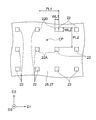
- FIG. 1 is a diagram for explaining a first specific example of the embodiment, and is a perspective view showing a display device and a surface light source device.
- FIG. 2 is a vertical cross-sectional view of the surface light source device of FIG.
- FIG. 3 is a plan view showing a plurality of light sources of the surface light source device of FIG.
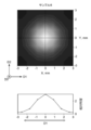
- FIG. 4 is a graph for explaining the diffusion characteristics due to the light diffusion portion of the diffusion member that can be included in the surface light source device of FIG. 2, and shows the angular distribution of the radiation intensity.
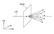
- FIG. 5 is a perspective view showing a light diffusing portion of the diffusing member that can be included in the surface light source device of FIG. 2, and is a diagram for explaining the light diffusing characteristics of the diffractive optical element forming the light diffusing portion.
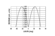
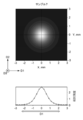
- FIG. 6 is a graph for explaining the light diffusion characteristics of the diffractive optical element of FIG. 5, and shows an angular distribution of radiant intensity.
- FIG. 7 is a vertical cross-sectional view showing an example of a microlens that can be included in the surface light source device of FIG.
- FIG. 8 is a vertical cross-sectional view showing another example of the microlens that may be included in the surface light source device of FIG.
- FIG. 9 is a vertical cross-sectional view showing still another example of the microlens that may be included in the surface light source device of FIG.
- FIG. 10 is a vertical cross-sectional view showing still another example of the microlens that may be included in the surface light source device of FIG.
- FIG. 10 is a vertical cross-sectional view showing still another example of the microlens that may be included in the surface light source device of FIG. FIG.
- FIG. 11A is a plan view showing an example of a specific configuration of a microlens that can be included in the surface light source device of FIG. 11B is a perspective view showing a unit optical element of the microlens of FIG. 11A.
- FIG. 12A is a plan view showing another example of a specific configuration of the microlens that may be included in the surface light source device of FIG. 12B is a perspective view showing a unit optical element of the microlens of FIG. 12A.
- FIG. 13A is a plan view showing an example of a specific configuration of a microlens that can be included in the surface light source device of FIG.
- FIG. 13B is a perspective view showing a unit optical element of the microlens of FIG. 13A.
- FIG. 13A is a plan view showing an example of a specific configuration of a microlens that can be included in the surface light source device of FIG.
- FIG. 13B is a perspective view showing a unit optical element of the microlen
- FIG. 14A is a plan view showing an example of a specific configuration of a microlens that can be included in the surface light source device of FIG. 14B is a perspective view showing a unit optical element of the microlens of FIG. 14A.
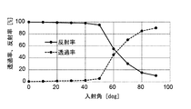
- FIG. 15 is a graph showing an example of the optical characteristics of the light reflecting portion of the diffusing member that can be included in the surface light source device of FIG. 2, and is a graph for explaining the reflection angle dependence of the reflectance and the transmittance. ..
- FIG. 16 is a graph showing another example of the optical characteristics of the light reflecting portion of the diffusing member that may be included in the surface light source device of FIG.
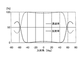
- FIG. 17 is a graph showing still another example of the optical characteristics of the light reflecting portion that may be included in the surface light source device of FIG.
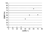
- FIG. 18 is an enlarged graph of a part of the graph of FIG.
- FIG. 19 is a vertical cross-sectional view showing a surface light source device, and is a diagram for explaining the operation of the diffusion member and the surface light source device.
- FIG. 20 is a vertical cross-sectional view of the surface light source device corresponding to FIG. 2, and is a diagram for explaining the operation of the diffusion member and the surface light source device.
- FIG. 21 is a vertical cross-sectional view of the surface light source device corresponding to FIG. 2, and is a diagram for explaining the operation of the diffusion member and the surface light source device.
- FIG. 22 is a vertical cross-sectional view of the surface light source device corresponding to FIG. 2, and is a diagram for explaining the operation of the diffusion member and the surface light source device.
- FIG. 20 is a vertical cross-sectional view of the surface light source device corresponding to FIG. 2, and is a diagram for explaining the operation of the diffusion member and the surface light source device.
- FIG. 23A is a simulation result of calculating the in-plane distribution of the illuminance of the surface light source device according to the sample 1.
- FIG. 23B is a simulation result of calculating the in-plane distribution of the illuminance of the surface light source device according to the sample 2.
- FIG. 23C is a simulation result of calculating the in-plane distribution of the illuminance of the surface light source device according to the sample 3.
- FIG. 23D is a simulation result of calculating the in-plane distribution of the illuminance of the surface light source device according to the sample 4.
- FIG. 23E is a simulation result of calculating the in-plane distribution of the illuminance of the surface light source device according to the sample 5.
- FIG. 23B is a simulation result of calculating the in-plane distribution of the illuminance of the surface light source device according to the sample 2.
- FIG. 23C is a simulation result of calculating the in-plane distribution of the illuminance of the surface light source device according to
- FIG. 23F is a simulation result of calculating the in-plane distribution of the illuminance of the surface light source device according to the sample 6.
- FIG. 23G is a simulation result of calculating the in-plane distribution of the illuminance of the surface light source device according to the sample 7.
- FIG. 24 is a diagram for explaining a second specific example of the embodiment, and is a vertical cross-sectional view showing an example of a diffusion member that can be included in the surface light source device of FIG.
- FIG. 25A is a vertical cross-sectional view showing an example of a microlens that can be included in the optical element portion of the diffusion member of FIG. 24.
- FIG. 25B is a vertical cross-sectional view showing another example of a microlens that may be included in the optical element portion of the diffusion member of FIG. 24.
- FIG. 26 is a perspective view showing another example of the optical element portion of the diffusion member of FIG. 24.
- FIG. 27 is a vertical cross-sectional view of the optical element portion corresponding to FIG. 25A, and is a diagram for explaining the operation of the optical element portion.
- FIG. 28 is a vertical cross-sectional view of the surface light source device corresponding to FIG. 2, and is a diagram illustrating an example in which the diffusion member includes a thermoplastic resin layer.
- FIG. 29 is a vertical cross-sectional view of the surface light source device corresponding to FIG.
- FIG. 30 is a side view illustrating an example of a method of manufacturing a light diffusing portion and an optical element portion that can be included in the diffusing member of FIG. 2 or FIG. 24.
- FIG. 31 is a diagram illustrating an example of a layer structure of a light diffusing portion that can be included in the diffusing member of FIG. 2 or FIG. 24.
- FIG. 32 is a diagram illustrating another example of a method of manufacturing a light diffusing portion and an optical element portion that may be included in the diffusing member of FIG. 2 or FIG. 24.
- FIG. 30 is a side view illustrating an example of a method of manufacturing a light diffusing portion and an optical element portion that can be included in the diffusing member of FIG. 2 or FIG. 24.
- FIG. 33 is a diagram illustrating an example of a layer structure of a light diffusing portion that can be included in the diffusing member of FIG. 2 or FIG. 24.
- FIG. 34 is a diagram showing the in-plane distribution of the radiation intensity on the light emitting surface of the surface light source device according to the first embodiment.
- FIG. 35 is a diagram showing the in-plane distribution of the radiation intensity on the light emitting surface of the surface light source device according to the second embodiment.
- FIG. 36 is a diagram showing the in-plane distribution of the radiation intensity on the light emitting surface of the surface light source device according to the third embodiment.
- FIG. 37 is a diagram showing the in-plane distribution of the radiation intensity on the light emitting surface of the surface light source device according to the fourth embodiment.
- FIG. 34 is a diagram showing the in-plane distribution of the radiation intensity on the light emitting surface of the surface light source device according to the first embodiment.
- FIG. 35 is a diagram showing the in-plane distribution of the radiation intensity on the light
- FIG. 38 is a diagram showing the in-plane distribution of the radiation intensity on the light emitting surface of the surface light source device according to the fifth embodiment.
- FIG. 39 is a diagram showing the in-plane distribution of the radiation intensity on the light emitting surface of the surface light source device according to the sixth embodiment.
- FIG. 40 is a diagram showing the in-plane distribution of the radiation intensity on the light emitting surface of the surface light source device according to Comparative Example 1.
- sheet is not distinguished from each other based only on the difference in designation.
- sheet is a concept that includes members that can be called “film” or “board”, and is not distinguished only by the difference in name.
- the normal direction of the sheet-shaped (sheet-shaped, plate-shaped) member refers to the normal direction of the target sheet-shaped (film-shaped, plate-shaped) member to the sheet surface.
- the "sheet surface (film surface, plate surface)” is a target sheet-like member (film-like) when the target sheet-like (film-like, plate-like) member is observed as a whole and from a broad perspective. Refers to a surface that coincides with the plane direction of the member (member, plate-shaped member).
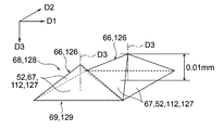
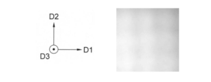
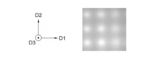
- the first direction D1, the second direction D2, and the stacking direction D3 are indicated by arrows as common directions between the drawings.
- the tip side of the arrow is one side of each direction D1, D2, D3.
- an arrow directed toward the back of the paper along the direction perpendicular to the paper of the drawing is indicated by a symbol with an X in the circle.
- an arrow pointing from the paper surface to the front along the direction perpendicular to the paper surface of the drawing is indicated by a symbol having dots in the circle.
- FIG. 1 is a perspective view schematically showing a display device 10 as an application example of the surface light source device 20 and the diffusion member 40.
- the display device 10 displays, for example, a moving image, a still image, character information, or an image composed of a combination thereof.
- the display device 10 can be used, for example, as an in-vehicle liquid crystal display device.
- the display device 10 can be used indoors or outdoors for various purposes such as advertising, presentations, television images, and display of various information.
- the display device 10 shown in FIG. 1 has a surface light source device 20 having a light emitting surface 20a and a display panel 15 arranged so as to face the light emitting surface 20a.
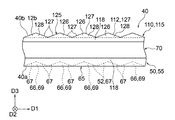
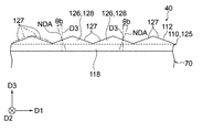
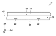
- FIG. 2 is a vertical cross-sectional view showing a surface light source device 20 as a first specific example.
- the surface light source device 20 has a light source 22 and a diffusion member 40 that adjusts the optical path of the light emitted from the light source 22 as main components.
- the diffusion member 40 is arranged so as to face the light source 22. That is, the diffusion member 40 is a sheet-like member and faces the light source 22 in the normal direction thereof.
- the diffusing member 40 can effectively eliminate the unevenness of brightness caused by the presence of the light source 22 by diffusing the light emitted from the light source 22.
- the illuminance at each position on the light emitting side surface 40b of the diffusion member 40 or the illuminance at each position on the virtual light receiving surface parallel to the light emitting side surface 40b located near the light emitting side surface 40b can be made uniform.
- the diffusion member 40 described in the present embodiment is devised to sufficiently make the in-plane distribution of brightness uniform while reducing the thickness of the surface light source device 20.
- the “illuminance on the light emitting side surface 40b” used in the following description means “illuminance on the light emitting side surface 40b” or “illuminance on the light receiving surface” described above.
- the display device 10 the surface light source device 20, and the diffusion member 40 in one embodiment will be described with reference to the illustrated first specific example.
- the display panel 15 of the display device 10 will be described. As shown in FIG. 1, the display panel 15 is laminated with the surface light source device 20 in the stacking direction D3. The display panel 15 is arranged so as to face the light emitting surface 20a of the surface light source device 20. The display panel 15 has a display surface 15a on which an image is displayed as a surface facing the side opposite to the surface light source device 20 in the stacking direction D3. In the illustrated example, the display panel 15 is formed in a rectangular shape when observed from the stacking direction D3, that is, in a plan view from the front direction.
- the display panel 15 is configured as, for example, a transmissive liquid crystal display panel. A part of the light incident from the surface light source device 20 is transmitted through the display panel 15 as a liquid crystal display panel, so that an image is displayed on the display surface 15a.
- the display panel 15 includes a liquid crystal layer having a liquid crystal material. The light transmittance of the display panel 15 changes according to the strength of the electric field applied to the liquid crystal layer.
- a liquid crystal display panel having a pair of polarizing plates and a liquid crystal cell (liquid crystal layer) arranged between the pair of polarizing plates can be used.
- the polarizing plate has a polarizer.
- the polarizer decomposes the incident light into two vertical polarization components.
- the polarization component in one direction passes through the polarizer.
- the polarization component in the other direction which is perpendicular to one direction, is absorbed by the polarizer.
- the liquid crystal cell has a pair of support plates and a liquid crystal display arranged between the pair of support plates. The liquid crystal cell is configured so that an electric field can be applied to each region forming one pixel.
- the orientation of the liquid crystal in the liquid crystal cell to which an electric field is applied changes.
- the polarized light component in a specific direction emitted from the surface light source device 20 and transmitted through the polarizing plate arranged on the surface light source device 20 side of the liquid crystal cell is polarized when passing through the liquid crystal cell to which no electric field is applied. Rotate the direction 90 °.
- the polarization component in a specific direction maintains its polarization direction when passing through a liquid crystal cell to which an electric field is applied.
- Whether the polarization component in a specific direction that has passed through one polarizing plate is further transmitted through the other polarizing plate or is absorbed by the other polarizing plate and blocked is controlled by the presence or absence of an electric field applied to the liquid crystal cell. can.
- the surface light source device 20 has a light emitting surface 20a that emits planar light.
- the surface light source device 20 is configured as a direct type backlight.
- the light source 22 is provided in the region overlapping the light emitting surface 20a.
- the normal direction of the display panel 15, the normal direction of the display surface 15a, the normal direction of the light emitting surface 20a, the normal direction of the diffusion member 40, and the light diffusion portion 50 included in the diffusion member 40 which will be described later.
- the normal directions of the light reflecting portion 70 and the optical element portion 110, and the normal directions of the support substrate 25 described later that supports the light source 22 are parallel to each other. In the illustrated example, these normal directions coincide with the stacking direction D3 and are also referred to as the front direction.
- the light source 22 has a light emitting element that emits light.
- a light emitting diode is exemplified as a light emitting element.
- the light emitting diode is also referred to as an LED.
- the dimensions of the light emitting diode used as the light source 22 are not particularly limited. From the viewpoint of making the image of the light source 22 inconspicuous, a small light emitting diode, for example, a mini LED or a micro LED may be used.
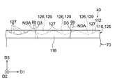
- the lengths WL1 and WL2 on one side of the light source 22 having a quadrangular shape in the observation from the stacking direction D3 shown in FIG. 3 may be preferably 0.5 mm or less, more preferably 0.2 mm or less. But it may be.
- the emission wavelength of the light source 22 can be appropriately selected according to the application of the surface light source device 20.
- the surface light source device 20 may have a light emitting element that emits blue light and a light emitting element that emits yellow light, and may generate white light.
- the surface light source device 20 may include a light emitting element that emits blue light, a light emitting element that emits green light, and a light emitting element that emits red light, and may generate white light.
- one light source 22 may include a plurality of types of light emitting elements arranged close to each other, or may include only a single light emitting element. That is, a plurality of types of light sources 22 having different emission wavelengths may be used.
- the light source 22 may include a light emitting diode that emits blue light having a wavelength of 450 nm as a light emitting element.
- a light emitting diode having a large output can be used as the light source 22.
- the light source 22 may be composed of only a light emitting element.
- the light source 22 may include an optical element such as a cover or a lens that adjusts the light distribution from the light emitting element in addition to the light emitting element, or absorbs the light from the light emitting element to emit light having a different wavelength. It may contain an emitting phosphor.
- the light distribution characteristics of the light source 22 are not particularly limited.
- the light distribution characteristic of the light source 22 may be a Lambertian light distribution. With the Lambertian light distribution, the highest peak intensity is obtained in the stacking direction D3, which is the optical axis, in the emission intensity distribution from the light source 22 directed to the stacking direction D3, and the peak is obtained in a direction inclined by 60 ° from the optical axis. Half the strength is obtained.
- the peak intensity may be obtained in a direction other than the stacking direction D3.
- the bad wing light distribution disclosed in Patent Document 1 JP6299811B
- Patent Document 1 JP6299811B
- the surface light source device 20 may have a plurality of light sources 22 or may have only a single light source 22.
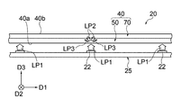
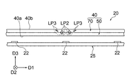
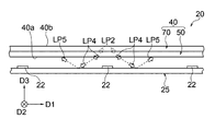
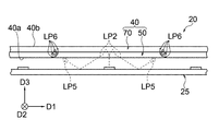
- the quantity of the light source 22 is appropriately selected according to the application of the surface light source device 20, the area of the light emitting surface 20a, and the like. From the viewpoint of eliminating the unevenness of brightness caused by the arrangement of the light sources 22, it is preferable that the plurality of light sources 22 included in the surface light source device 20 are regularly arranged on the surface perpendicular to the stacking direction D3.
- a plurality of light sources 22 are arranged in a honeycomb array arranged at a constant pitch in each of three directions inclined by 60 ° with each other, or in a square array arranged at a constant pitch in each of two directions perpendicular to each other. May be arranged.
- the plurality of light sources 22 are arranged at a constant pitch in each of the first direction D1 and the second direction D2 perpendicular to each other.
- the array pitch PL1 in the first direction D1 and the light distribution pitch PL2 of the light source 22 in the second direction D2 are the same.
- the example is not limited to the illustrated example, and the array pitch PL1 and the array pitch PL2 may be different.
- the first direction D1 and the second direction D2 are parallel to the side edges of the rectangular surface light source device 20 and the diffusion member 40, respectively.
- the array pitch PL1 and the array pitch PL2 of the light source 22 may be 0.2 mm or more and 10 mm or less, respectively.
- the light source 22 may emit only P-polarized light when it enters the diffusion member 40.
- the P-polarized light is light that vibrates on a surface including the traveling direction of the light when it is incident on the diffusing member 40 and the normal direction of the diffusing member 40 to the incoming light side surface 40a.
- the illustrated surface light source device 20 further has a support substrate 25 that supports the light source 22 in addition to the light source 22 and the diffusion member 40.
- the support substrate 25 supports a plurality of light sources 22 from the side opposite to the diffusion member 40 in the stacking direction D3.
- the support substrate 25 includes a circuit that supplies electric power to the light source 22.
- the support substrate 25 is a sheet-like member.
- the support substrate 25 has a light reflectivity that reflects light and directs it toward the diffusion member 40.
- the light reflectivity of the support substrate 25 is not particularly limited as long as it is exhibited with respect to the light emitted from the light source 22 or the light used for light emission by the surface light source device 20.
- the light used for light emission in the surface light source device 20 may include light emitted from the light source 22 and wavelength-converted.
- the sheet-shaped substrate main body 26, the reflective layer 27 laminated on the substrate main body 26 from the diffusion member 40 side in the stacking direction D3, and the light source 22 are electrically connected. It has a wiring 28 and.
- the substrate body 26 extends in a direction perpendicular to the stacking direction D3, and the substrate body 26 has an insulating property.
- the reflective layer 27 is reflective to the light emitted from the light source 22 or to the light used for light emission by the surface light source device 20.
- the reflectivity of the reflective layer 27 may be regular reflection, which is also called specular reflection, diffuse reflection, or anisotropic diffuse reflection.
- the substrate body 26 may be a resin film containing diffusion particles, for example, a film made of white polyethylene terephthalate.
- the reflective layer 27 may be a metal layer laminated on the substrate main body 26, or may be a reflective diffractive optical element.
- the wiring 28 is electrically connected to a terminal (not shown) of the light source 22 via solder or the like. When the substrate body 26 and the reflective layer 27 have an insulating property, the wiring 28 is preferably located between the substrate body 26 and the reflective layer 27.
- the light source 22 may be covered with the sealing material 23.
- the sealing material 23 is provided corresponding to each light source 22.
- the encapsulant 23 is two-dimensionally arranged in the same manner as the light source 22.
- the light source 22 has a surface and a side surface facing the diffusion member 40 covered with a sealing material 23.
- the sealing material 23 is fixed to the support substrate 25.
- the portion where the light source 22 and the wiring 28 are electrically connected may also be covered with the sealing material 23.
- a thermosetting resin such as a silicone resin or an epoxy resin
- a thermoplastic resin such as an olefin resin
- the diffusion member 40 is arranged on the sealing material 23. That is, the diffusion member 40 is supported by the sealing material 23 and is separated from the light source 22 and the support substrate 25 in the stacking direction D3.
- the sealing material 23 may be bonded to the diffusion member 40 by adhesion, adhesion, welding or the like.
- the distance DX shown in FIG. 2 is the distance between the light source 22 and the diffusion member 40 along the stacking direction D3. In other words, the distance DX refers to the distance along the stacking direction D3 between the surface of the light source 22 facing the diffusion member 40 side and the light incoming side surface 40a of the diffusion member 40.
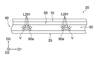
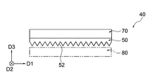
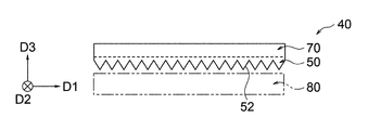
- the diffusion member 40 has a light diffusion unit 50 and a light reflection unit 70 in this order.
- the light diffusing unit 50 is located on the light input side of the light to be diffused by the diffusing member 40 with the light reflecting unit 70 as a reference.
- the light reflecting unit 70 is located on the light emitting side of the light to be diffused by the diffusing member 40 with the light diffusing unit 50 as a reference.
- the diffusion member 40 has a sheet shape.
- the diffusion member 40 extends in the first direction D1 and the second direction D2 perpendicular to the stacking direction D3.
- the light diffusing portion 50 forms the light entering side surface 40a of the diffusing member 40.
- the light reflecting portion 70 forms the light emitting side surface 40b of the diffusion member 40.
- the light diffusing portion 50 and the light reflecting portion 70 may be joined to each other, may be merely in contact with each other and may not be joined to each other, and may be separated from each other. ..
- the light diffusing unit 50 has light transmissivity and light diffusing property with respect to the light emitted from the light source 22 or the light used for light emission by the surface light source device 20.
- the light diffusing unit 50 has light transmissivity and light diffusing property with respect to visible light.
- the light diffusing portion 50 may include an optical sheet 55 that is simply overlapped with another member or bonded to another member by adhesion or adhesion, may be an optical sheet 55, or may be an optical sheet 55, a member, a structure, or the like. It may be a part, or may be a surface of an optical sheet, a member, a structure, or the like.
- the total light transmittance of the light diffusing unit 50 is preferably 50% or more, more preferably 70% or more, and further preferably 90% or more.
- the utilization efficiency of the light from the light source 22 is improved.
- the light diffusing unit 50 is applied to the surface light source device 20, the in-plane distribution of the illuminance on the light emitting side surface 40b of the diffusing member 40 can be effectively made uniform. Therefore, the light diffusing unit 50 is made of a material having high transparency to the light emitted from the light source 22 or to the light used for light emission by the surface light source device 20.
- the total light transmittance is a value measured by a method based on JIS K7361-1: 1997, with the incident angle set to 0 degree.
- the total light transmittance is a value measured using an ultraviolet-visible near-infrared spectrophotometer V-7200 manufactured by JASCO Corporation.
- the light diffusivity of the light diffusing unit 50 may be isotropic diffusion or anisotropic diffusion.
- the light diffusing unit 50 may diffuse light in a direction within a specific angle range.
- the specific angle range may be one, or may be plural apart from each other.
- the diffusion by the light diffusing unit 50 is not limited to diffusing the transmitted light, and the reflected light may be diffused.
- the diffusion angle ⁇ of the light incident on the light diffusing unit 50 is preferably 10 ° or more, more preferably 15 ° or more, and further preferably 20 ° or more.
- the diffusion angle of the light incident on the light diffusion unit 50 is preferably 85 ° or less, more preferably 60 ° or less, and even more preferably 50 ° or less.
- the diffusion angle ⁇ is the half-value full width (FWHM) in the angular distribution of the radiant intensity (watt / steradian) obtained when light is incident on the light entry side surface of the light diffusion unit 50 at an incident angle of 0 °. ..
- FIG. 4 is a graph showing an angular distribution of radiation intensity on the light emitting side surface of the light diffusing portion 50 when a parallel light flux is incident on the incident side surface of the light diffusing portion 50 at an incident angle of 0 °.
- the vertical axis is the value of radiant intensity
- the horizontal axis is the emission angle.
- the half-value full width in the angular distribution of radiant intensity corresponding to each diffusion ⁇ is the width (°) of the range of the emission angle at which half of the maximum transmitted light intensity I max in the angular distribution of radiant intensity can be obtained.
- the angular distribution of radiant intensity can be measured using a variable angle photometer or a variable angle spectrophotometer.
- a variable angle photometer (goniophotometer) GP-200 manufactured by Murakami Color Technology Research Institute can be used.
- the incident angle means the angle (°) formed by the traveling direction of the incident light with respect to the normal direction of the sheet-like member to which the light is incident.
- the emission angle means an angle (°) formed by the traveling direction of the emitted light with respect to the normal direction of a member such as a sheet from which the light is emitted.
- FIG. 5 is a perspective view for explaining another preferable light diffusing characteristic of the light diffusing portion 50, which has a light diffusing property different from that of FIG.
- the light ray L51 is incident on the light diffusing portion 50 at an incident angle of 0 °. That is, the light ray L51 is vertically incident on the light diffusing portion 50.
- the light ray L51 is diffused by optical actions such as refraction, reflection, and diffraction in the light diffusing portion 50. According to the light diffusing portion 50 shown in FIG.
- the light ray L51 is mainly a circle from the apex to the bottom surface of a cone whose apex is located on the light diffusing portion 50 and whose bottom surface is arranged parallel to the light diffusing portion 50. It is traveling along the optical path toward each position on the circumference.
- the radiant intensity on the side of the light diffusing portion 50 facing the light reflecting portion 70 has a peak at an emission angle other than 0 °. ..
- the radiation intensity on the side of the light diffusing portion 50 facing the light reflecting portion 70 is the emission direction in which the emission angle is 0 °. It has a peak at an emission angle other than 0 ° in the angle distribution in any plane including.
- the absolute value of the emission angle having a peak of radiant intensity may be preferably 30 ° or more and 60 ° or less, more preferably 30 ° or more and 50 ° or less, and further preferably 30 ° or more and 45 ° or less.
- the absolute value of the emission angle of 90% or more of the light incident on the light diffusing unit 50 at an incident angle of 0 ° may be 30 ° or more and 60 ° or less.
- the absolute value of the emission angle of 95% or more of the light incident on the light diffusing unit 50 at an incident angle of 0 ° may be 30 ° or more and 60 ° or less.
- the absolute value of the emission angle of 98% or more of the light may be 30 ° or more and 60 ° or less.
- the diffusing member 40 suppresses the illuminance in the region directly above the light source 22 from becoming too high, and is perpendicular to the stacking direction D3.
- the illuminance in the region separated from the light source 22 in the above direction can be increased.
- the in-plane distribution of illuminance can be effectively made uniform.
- the reflectance of the light incident on the light reflecting unit 70 which will be described later, at an incident angle of 0 ° or more and a peak angle or less in absolute value is preferable. It is 80% or more. It is more preferably 85% or more, and further preferably 90% or more.
- the peak angle means an absolute value of an emission angle having a peak of radiant intensity.
- the solid line in FIG. 6 is a graph showing the angular distribution of the radiation intensity on the light emitting side surface of the light diffusing portion 50 shown in FIG. 5 when the incident angle of the incident light is 0 °.
- the light diffusing unit 50 is not particularly limited, and various configurations having light transmissivity and light diffusing property can be adopted.
- the light diffusing unit 50 may include at least one of a transmissive diffractive optical element 60 and a microlens 65.
- the diffractive optical element 60 is an element that exerts a diffractive action on incident light.
- the diffractive optical element 60 may be a hologram element.
- a diffractive optical element having diffractive properties for achieving the desired light diffusivity can be designed relatively easily.
- the diffractive optical element 60 may have the diffusion characteristics shown in FIG.
- the microlens 65 has a plurality of unit optical elements 66.
- the unit optical element 66 is an element that changes the traveling direction of light by refraction, reflection, or the like.
- the unit optical element 66 is a concept including an element called a unit shape element, a unit prism, and a unit lens.
- the unit optical element 66 is configured as a convex portion 68 or a concave portion 69.
- the light diffusing portion 50 has a main body portion 58, and a unit optical element 66 as a convex portion 68 is formed in the main body portion 58.
- the light diffusing portion 50 may have a main body portion 58 and a unit optical element 66 as a recess 69 provided on the main body portion 58.
- the main body 58 has a sheet shape.
- the main body 58 extends in the first direction D1 and the second direction D2 perpendicular to the stacking direction D3. In the example shown in FIG. 2, the main body portion 58 is joined to the light reflecting portion 70.
- the unit optical element 66 has an element surface 67 inclined with respect to the stacking direction D3.
- the unit optical element 66 is defined by the element surface 67.
- the microlens 65 has an uneven surface 52 formed by the element surface 67 of the unit optical element 66.
- the microlens 65 can bend the traveling direction of the incident light by the uneven surface 52.
- the uneven surface 52 may face either direction in the stacking direction D3.
- the uneven surface 52 faces the light source 22 in the stacking direction D3.
- the uneven surface 52 faces the light reflecting portion 70 in the stacking direction D3.
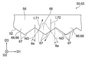
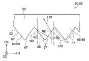
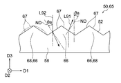
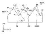
- the uneven surface 52 can bend the traveling direction of the light L71, L81, L91, L101 incident from the light source 22 side, and can change the traveling direction of the light L72, L82, L92, L102 incident from the light reflecting portion 70 side. Can be bent. In particular, as shown in FIGS.
- the microlens 65 bends the traveling direction of the incident light from a direction having a small inclination angle with respect to the stacking direction D3, and makes the inclination angle with respect to the stacking direction D3 larger than that at the time of incident. Can be done. That is, the inclination angle formed by the traveling direction of the light emitted from the light diffusing portion 50 with respect to the stacking direction D3 is made larger than the inclination angle formed by the traveling direction of the incident light to the light diffusing portion 50 with respect to the stacking direction D3. be able to.
- the traveling direction of the light is changed by refracting the lights L71, L72, L91, and L92 at the element surface 67.
- the traveling direction of the light is changed by reflecting the lights L82 and L101 on the element surface 67, preferably by total internal reflection.
- the change in the traveling direction due to the reflection shown in FIGS. 8 and 10 tends to be larger than the change in the traveling direction due to the refraction shown in FIGS. 7 and 9.
- the more the normal direction ND of the element surface 67 is inclined with respect to the stacking direction D3, in other words, the more the element surface 67 rises in the stacking direction D3, the more easily the light is reflected by the element surface 67.
- the normal direction ND of the element surface 67 forms an inclination angle ⁇ a larger than 45 ° with respect to the stacking direction D3
- the light not significantly inclined with respect to the stacking direction D3 is the element surface 67.
- the traveling direction of the light is greatly inclined with respect to the stacking direction D3 due to the reflection at.
- the unit optical element 66 may include an element surface 67 having a normal direction ND inclined at an inclination angle ⁇ a larger than 45 ° with respect to the stacking direction D3. .. Since the element surface 67 rises in the stacking direction D3, reflection, preferably total reflection, is likely to occur. That is, according to the unit optical element 66 including the element surface 67, the optical path of the light transmitted through the microlens 65 can be greatly bent by reflection, preferably by total reflection. By greatly adjusting the traveling direction of light, the in-plane distribution of illuminance can be more effectively homogenized.
- the diffusion characteristic of the microlens 65 is affected by the tilt angle ⁇ a of the element surface 67 of the unit optical element 66. Therefore, the cross-sectional shape of the microlens 65 can be appropriately adjusted based on the optical characteristics required for the surface light source device 20 and the diffusion member 40.
- the inclination angles ⁇ a of the plurality of element surfaces 67 included in one unit optical element 66 may be different from each other or may be the same.
- the plurality of unit optical elements 66 included in the microlens 65 may be different from each other in the configuration such as shape, orientation, and size.
- a plurality of unit optical elements 66 included in the microlens 65 may have the same configuration as each other.
- the inclination angle ⁇ a is preferably 25 ° or less, more preferably 20 ° or less, still more preferably 15 °. It is as follows.
- the element surface 67 may be slightly curved.
- the unit optical element 66 may have an outer shape of a part of a sphere such as a hemisphere, or may have an outer shape of a part of a spheroid.
- the optical path of the light transmitted through the microlens 65 is bent in various directions due to reflection or refraction.
- the in-plane distribution of illuminance can be more effectively made uniform.
- the change in the angular distribution of radiant intensity can be effectively smoothed.
- the unit optical element 66 may include an element surface 67 formed as a matte surface.
- the element surface 67 as a matte surface scatters light in various directions.
- the in-plane distribution of illuminance can be more effectively made uniform.
- the change in the angular distribution of radiant intensity can be effectively smoothed.
- the plurality of unit optical elements 66 included in the microlens 65 are two-dimensionally arranged. Therefore, the element surface 67 of the unit optical element 66 included in the microlens 65 faces in various directions. As a result, the microlens 65 can guide light in various directions by the two-dimensionally arranged unit optical elements 66.
- the plurality of unit optical elements 66 may be arranged irregularly or may be arranged regularly. By regularly arranging the plurality of unit optical elements 66, the design of the microlens 65 becomes easy, and the unit optical elements 66 can be easily spread without gaps.
- microlens 65 a plurality of specific examples of the microlens 65 will be described with reference to FIGS. 11A to 14B.
- the microlens 65 shown in these figures was the subject of the simulation described later.
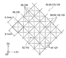
- the arrangement of the plurality of unit optical elements 66 is a square arrangement.
- the plurality of unit optical elements 66 are arranged in the first direction D1 at a constant pitch.
- the plurality of unit optical elements 66 are also arranged at a constant pitch in the second direction D2.
- the arrangement pitch in the first direction D1 and the arrangement pitch in the second direction D2 may be the same or different.
- the arrangement pitch in the first direction D1 and the arrangement pitch in the second direction D2 are the same as each other and are 0.1 mm.
- each unit optical element 66 has a shape in which the bottom of the cone is cut off from all sides.
- the cone is arranged at a placement pitch shorter than the diameter of the bottom surface of the cone shown by the dotted line in FIG. 11A, and the portion where the adjacent cones overlap in the first direction D1 and the second direction D2 is cut off to form the microlens 65. It has been made.
- the plurality of unit optical elements 66 are spread without gaps.
- the height of each unit optical element 66 in the stacking direction D3 is 0.09 mm as an example.
- the illustrated unit optical element 66 has an element surface 67 that corresponds to the side surface of the cone.
- Each unit optical element 66 can diffuse light radially when observed from the stacking direction D3.
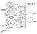
- the arrangement of the plurality of unit optical elements 66 is a square arrangement.
- the plurality of unit optical elements 66 are arranged at a constant pitch in two directions inclined by ⁇ 45 ° with respect to the first direction D1.
- the arrangement pitch in each direction may be the same or different.
- the arrangement pitches of the unit optical elements 66 in the two directions are the same as each other and are 0.1 mm.
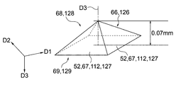
- the unit optical element 66 has a quadrangular pyramid shape having a square bottom surface.
- the height of each unit optical element 66 in the stacking direction D3 is 0.07 mm as an example.
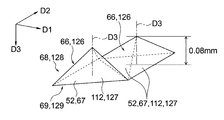
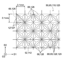
- the microlens 65 has two types of unit optical elements 66.
- the unit optical elements 66 of each type are arranged at a constant pitch in the second direction D2 and two directions inclined by ⁇ 60 ° with respect to the second direction. That is, the two types of unit optical elements 66 are arranged at a constant pitch in each of the three directions inclined by 60 ° with respect to each other.
- the array of unit optical elements 66 shown is also referred to as a honeycomb array.
- the arrangement pitch in each direction may be the same or different. In the illustrated example, the arrangement pitches of the unit optical elements 66 in the three directions are the same as each other.
- the shapes of the bottom surfaces of the two types of unit optical elements 66 are the same.
- the shape of the bottom is an equilateral triangle.
- the orientation of the bottom surface of the two types of unit optical elements 66 is different. When one unit optical element 66 is rotated by 60 °, the orientation of the bottom surface of one unit optical element 66 coincides with the orientation of the bottom surface of the other unit optical element 66.
- the unit optical element 66 has the shape of a triangular pyramid whose bottom surface is an equilateral triangle.
- the height of the bottom surface of the unit optical element 66 is 0.1 mm as an example.
- the height of the unit optical element 66 is 0.08 mm as an example.
- Each unit optical element 66 may have a regular triangular pyramid shape.
- the unit optical elements 66 having the same bottom surface are arranged in four directions.
- the plurality of unit optical elements 66 having the same shape and orientation of the bottom surface are arranged at a constant pitch in each of the first direction D1 and the second direction D2.
- the arrangement pitches in the two directions may be the same or different.
- the arrangement pitch in each of the two directions is the same.
- the unit optical element 66 has a triangular pyramid shape whose bottom surface is a right-angled isosceles triangle shape.
- the length of the equilateral sides of the right-angled isosceles triangle forming the bottom surface is 0.1 mm as an example.
- the height of the unit optical element 66 is 0.01 mm as an example.
- the perpendicular line from the apex to the bottom surface of the cone forming the unit optical element 66 may pass through the center of gravity of the bottom surface.
- the unit optical element 66 projects toward the light source 22 in the stacking direction D3. That is, the unit optical element 66 is a convex portion 68 protruding from the main body portion 58.
- the unit optical element 66 may be a recess 69 formed in the main body 58.
- the maximum length of the unit optical element 66 in the direction perpendicular to the stacking direction D3 is preferably 1.5 mm or less, more preferably 1 mm or less, still more preferably 0.5 mm. It is as follows.
- one unit optical element 66 may have a dimension smaller than the dimension obtained by triple the light source 22 in each of the two directions perpendicular to each other when observed from the stacking direction D3. preferable.
- the lengths WL1 and WL2 of one side of the light source 22 having a quadrangular shape in the observation from the stacking direction D3 shown in FIG. 3 are preferably 0.5 mm or less, more preferably 0.2 mm or less.
- the unit optical element 66 preferably has a dimension smaller than a 1.5 mm square, and more preferably a dimension smaller than a 0.6 mm square.
- one dimension is smaller than the other dimension, it means that one outer contour is located on the other outer contour or inside the other outer contour in at least one direction. ..
- the dimension of the unit optical element 66 along an arbitrary direction may be three times or less the dimension of the light source 22 along the direction.
- the light emitted from the diffusing member 40 using these unit optical elements 66 is constant without depending on the relative position between the diffusing member 40 and the light source 22 along the directions D1 and D2 perpendicular to the stacking direction D3. It comes to have light distribution characteristics. That is, the surface light source device 20 can be assembled without positioning the diffusion member 40 and the light source 22 along the directions D1 and D2 perpendicular to the stacking direction D3. That is, the diffusion member 40 can be arranged on the light source 22 by alignment-free.
- the arrangement pitch of the unit optical elements 66 having such dimensions may be 0.01 mm or more and 1.5 mm or less.
- the arrangement pitch of the unit optical elements 66 is preferably 0.05 mm or more and 1 mm. It is less than or equal to, more preferably 0.1 mm or more and 0.5 mm or less.
- the microlens 65 is observed from the stacking direction D3 in the normal direction ND to the element surface 67. Diffuses light. In other words, the microlens 65 guides light in the normal direction ND of the element surface 67 observed from the stacking direction D3.
- the arrangement interval of the plurality of light sources 22 becomes shorter along the arrangement direction of the light sources 22, but becomes longer in a direction non-parallel to the arrangement direction of the light sources 22.
- the unit optical element 66 has a normal direction ND that is non-parallel to the arrangement direction of the plurality of light sources 22 when observed from the stacking direction D3. Includes surface 67. More preferably, the unit optical element 66 has a normal direction ND inclined at an angle of 35 ° or more and 55 ° or less with respect to the arrangement direction of the plurality of light sources 22 in the observation from the stacking direction D3, and the element surface 67 is formed. Includes. According to such an arrangement, light can be effectively diffused in a direction non-parallel to the arrangement direction of the plurality of light sources 22 by reflection or refraction at the unit optical element 66. As a result, the in-plane distribution of illuminance can be more effectively made uniform.
- the unit optical element 66 has four element surfaces 67.
- the normal direction NDs of the four element surfaces 67 are all inclined by 45 ° with respect to the first direction D1 and the second direction D2, which are the arrangement directions of the light sources 22.
- the position CP at the center of the four adjacent light sources 22 tends to be the darkest.
- the four light sources 22 include two light sources 22A adjacent to one arrangement direction D1 and two other light sources 22B adjacent to the two light sources 22A from one side in the other arrangement direction D2, respectively. ..
- light can be efficiently guided towards this darkest position CP, effectively uniformizing the in-plane distribution of illuminance.
- the diffusion member 40 may be provided with a display 42 (see FIG. 1) indicating the direction in which the diffusion member 40 should be arranged.
- the display 42 functions as a so-called alignment mark.
- the display 42 provided on the diffusion member 40 may display the direction of the element surface 67 in the normal direction ND.
- the display 42 may indicate a preferred direction in which the diffusion member 40 should be arranged with respect to the light source 22 or the support substrate 25.
- the display 42 may display a preferred arrangement direction of the light sources 22 with respect to the diffusion member 40.
- a display related to the arrangement direction of the light source 22 is provided on the support substrate 25, and the diffusion member 40 is positioned in an appropriate direction with respect to the arrangement of the light source 22 based on the display of the support substrate 25 and the display 42 of the diffusion member 40. You may.
- the light diffusing unit 50 may include a microlens 65 having a plurality of unit optical elements 66 arranged in a direction non-parallel to the arrangement direction of the plurality of light sources 22. That is, the arrangement direction of the plurality of unit optical elements 66 may be non-parallel to the arrangement direction of the plurality of light sources 22. According to such an arrangement, moire caused by the superposition of the arrangement of the unit optical elements 66 and the arrangement of the light source 22 can be effectively made inconspicuous.
- the diffractive optical element 60 and the microlens 65 that can be used in the light diffusing unit 50 have been described.
- the diffractive optical element 60 and the microlens 65 are merely examples, and other elements having both light transmission and light diffusivity may be used as the light diffusing unit 50.
- the above-mentioned elements having specific properties of light transmission and light diffusivity may be preferably used as the light diffusing unit 50.
- an optical sheet or the like having a light transmitting base material and light diffusing particles dispersed in the base material may be used as the light diffusing unit 50.
- the light reflecting portion 70 is located on the opposite side of the light diffusing portion 50 from the light source 22 in the stacking direction D3.
- the light reflecting unit 70 has a light reflecting property that reflects visible light. The reflectance and transmittance of the light reflecting unit 70 change depending on the incident angle.
- the transmittance of the light of a specific wavelength incident at an incident angle of 0 ° at the light reflecting unit 70 is larger than the transmittance of the light of a specific wavelength incident at an incident angle larger than 0 ° at the light reflecting unit 70. small. That is, the transmittance of the vertically incident specific wavelength light in the light reflecting unit 70 is smaller than the transmittance of the light reflecting unit 70 of the specific wavelength light incident from at least one oblique direction.
- the reflectance of the light of a specific wavelength incident at an incident angle of 0 ° at the light reflecting unit 70 is larger than the reflectance of the light of a specific wavelength incident at an incident angle larger than 0 ° at the light reflecting unit 70. big.
- the light reflecting unit 70 can also be described as a selective light reflecting unit, a light transmitting unit, and a selective light transmitting unit.
- the light reflecting unit 70 reflects light of a specific wavelength incident at an incident angle of 0 ° with a reflectance of 80% or more.
- the light reflecting unit 70 transmits light of a specific wavelength incident at an incident angle of 0 ° with a transmittance of less than 20%. Further, the light reflecting unit 70 reflects light of at least a part of a specific wavelength incident at an incident angle larger than 45 ° in absolute value with a reflectance lower than 50%.
- the light reflecting unit 70 transmits light of at least a part of a specific wavelength incident at an incident angle larger than 45 ° in absolute value with a transmittance of 50% or more.
- the light reflecting unit 70 has an incident angle dependence of the reflectance. Further, the light reflecting unit 70 has an incident angle dependence of the transmittance.
- FIG. 15 is a graph showing an example of reflection characteristics and transmission characteristics according to the incident angle of the light reflecting unit 70.
- the reflectance of light of a specific wavelength having an incident angle of 70 ° or more and less than 90 ° in absolute value at the light reflecting portion 70 may be less than 70%, less than 60%, or less than 50%.
- the reflectance of light of a specific wavelength having an incident angle of 60 ° or less in the light reflecting portion 70 may be 50% or more and less than 100%, 80% or more and less than 100%, and 90% or more and less than 100%. It's fine.
- the reflectance of light of a specific wavelength having an incident angle of 0 ° at the light reflecting portion 70 may be 80% or more and less than 100%, 90% or more and less than 100%, or 95% or more and less than 100%.
- the transmittance of light of a specific wavelength in the light reflecting unit 70 decreases.
- the transmittance of light having a specific wavelength having an incident angle of 70 ° or more and less than 90 ° in the light reflecting portion 70 may be 30% or more, 40% or more, or 50% or more.
- the transmittance of light of a specific wavelength having an incident angle of 60 ° or less in the light reflecting portion 70 may be 0% or more and less than 50%, 0% or more and less than 20%, and 0% or more and less than 10%. But it may be.
- the transmittance of light of a specific wavelength having an incident angle of 0 ° at the light reflecting portion 70 may be 0% or more and less than 20%, 0% or more and less than 10%, or 0% or more and less than 5%.
- the light of a specific wavelength can be appropriately set according to the application of the surface light source device 20 and the diffusion member 40.
- the light emitted from the light source 22 or the light used for light emission by the surface light source device 20 may be light having a specific wavelength.
- Light of a specific wavelength may be visible light.
- "Visible light” means light having a wavelength of 380 nm or more and a wavelength of 780 nm or less.
- the reflectance of the light reflecting portion shall be a value measured using a variable angle photometer (goniophotometer) GP-200 manufactured by Murakami Color Technology Research Institute.
- the transmittance of the light reflecting portion is the total light transmittance measured in accordance with JIS K7361-1: 1997.
- the transmittance of the light reflecting portion shall be a value measured using a variable angle photometer (goniophotometer) GP-200 manufactured by Murakami Color Technology Research Institute.
- FIG. 16 is a graph showing another example of the optical characteristics of the light reflecting portion.
- the light reflecting unit having the optical characteristics shown in FIG. 16 is different from the light reflecting unit having the optical characteristics shown in FIG.
- FIG. 16 is a graph showing the reflection characteristics and transmission characteristics of the light reflecting portion for light having a wavelength of 450 nm, which is blue light.
- the reflectance of the light of a specific wavelength whose incident angle is 0 ° or more and 30 ° or less in absolute value at the light reflecting portion 70 may be 80% or more, 90% or more, and 95%. The above may be sufficient.
- the reflectance of the light of a specific wavelength having an incident angle of 0 ° or more and 45 ° or less in absolute value at the light reflecting portion 70 may be 80% or more, 85% or more, or 90% or more. According to such reflection characteristics, the combination with the light diffusing unit 50 effectively prevents the illuminance in the region directly above the light source 22 from becoming too high, and effectively equalizes the in-plane distribution of the illuminance. can.
- the transmittance of light of a specific wavelength having an incident angle of 0 ° or more and 30 ° or less in the light reflecting portion 70 may be less than 20%, less than 10%, or 5%. It may be less than.
- the transmittance of light having a specific wavelength having an incident angle of 0 ° or more and 45 ° or less in the light reflecting portion 70 may be less than 20%, less than 15%, or less than 10%. According to such transmission characteristics, the combination with the light diffusing unit 50 effectively prevents the illuminance in the region directly above the light source 22 from becoming too high, and effectively equalizes the in-plane distribution of the illuminance. can.
- the reflectance of light of a specific wavelength incident at a certain incident angle of 45 ° or more and 75 ° or less in absolute value at the light reflecting portion 70 may be 50%.
- the reflectance of light of a specific wavelength incident at a certain incident angle, which is 50 ° or more and 60 ° or less in absolute value, at the light reflecting portion 70 may be 50%.
- the absolute value of the incident angle increases in the range of 50 ° or more and 60 ° or less, the reflectance of light of a specific wavelength at the light reflecting portion may decrease. In the region separated from the light source 22 in the direction perpendicular to the stacking direction D3, a relatively large amount of light travels in a direction inclined with respect to the stacking direction D3.
- the illuminance in the region separated from the light source 22 can be increased and the in-plane distribution of the illuminance can be effectively made uniform by combining with the diffusion characteristics of the light diffusing portion 50. ..
- the transmittance of light of a specific wavelength incident at a certain incident angle of 45 ° or more and 75 ° or less in absolute value at the light reflecting portion 70 may be 50%.
- the transmittance of light of a specific wavelength incident at a certain incident angle, which is 50 ° or more and 60 ° or less in absolute value, at the light reflecting portion 70 may be 50%.
- the absolute value of the incident angle increases in the range of 50 ° or more and 60 ° or less
- the transmittance of light of a specific wavelength at the light reflecting portion may increase.
- the illuminance in the region separated from the light source 22 can be increased and the in-plane distribution of the illuminance can be effectively made uniform by combining with the diffusion characteristics of the light diffusion unit 50. ..
- FIGS. 17 and 18 are graphs showing still another example of the optical characteristics of the light reflecting portion.
- the light reflecting unit having the optical characteristics shown in FIGS. 17 and 18 is different from the light reflecting unit having the optical characteristics shown in FIG. 16 and different from the light reflecting unit having the optical characteristics shown in FIG. 17 and 18 are graphs showing the transmission characteristics of the light reflecting portion for light having a wavelength of 450 nm, which is blue light.
- the transmittance of light of a specific wavelength having an incident angle of 0 ° or more and 30 ° or less in the light reflecting portion 70 may be less than 15% or less than 8%. It may be less than 3%.
- the transmittance of light having a specific wavelength having an incident angle of 0 ° or more and 45 ° or less in the light reflecting portion 70 may be less than 50%, less than 40%, or less than 30%. According to such a transmission characteristic, the combination with the diffusion characteristic of the light diffusing portion 50 effectively prevents the illuminance in the region directly above the light source 22 from becoming too high, and effectively distributes the illuminance in the plane. Can be made uniform.
- the reflectance of light of a specific wavelength whose incident angle is 0 ° or more and 30 ° or less in absolute value at the light reflecting unit 70 may be 85% or more, 92% or more, or 97% or more.
- the reflectance of the light of a specific wavelength having an incident angle of 0 ° or more and 45 ° or less in absolute value at the light reflecting portion 70 may be 50% or more, 60% or more, or 70% or more. According to such a reflection characteristic, by combining with the diffusion characteristic of the light diffusing portion 50, it is possible to effectively prevent the illuminance in the region directly above the light source 22 from becoming too high, and the in-plane distribution of the illuminance is effective. Can be made uniform.
- the transmittance of light of a specific wavelength incident at a certain incident angle of 40 ° or more and 60 ° or less in absolute value at the light reflecting portion 70 may be 50%.
- the transmittance of light of a specific wavelength incident at a certain incident angle, which is 45 ° or more and 55 ° or less in absolute value, at the light reflecting portion 70 may be 50%.
- the absolute value of the incident angle increases in the range of 30 ° or more and 60 ° or less
- the transmittance of light of a specific wavelength at the light reflecting portion may increase.
- the absolute value of the incident angle increases in the range of 50 ° or less
- the transmittance of light of a specific wavelength at the light reflecting portion may increase.
- the illuminance in the region separated from the light source 22 is increased by combining with the diffusion characteristics of the light diffusion unit 50, and the illuminance surface.
- the internal distribution can be effectively made uniform.
- the reflectance of light of a specific wavelength incident at a certain incident angle of 40 ° or more and 60 ° or less in absolute value at the light reflecting portion 70 may be 50%.
- the reflectance of light of a specific wavelength incident at a certain incident angle, which is 45 ° or more and 55 ° or less in absolute value, at the light reflecting portion 70 may be 50%.
- the absolute value of the incident angle increases in the range of 30 ° or more and 60 ° or less, the reflectance of light of a specific wavelength at the light reflecting portion may decrease.
- the absolute value of the incident angle increases in the range of 50 ° or less, the reflectance of light of a specific wavelength at the light reflecting portion may decrease.
- the illuminance in the region separated from the light source 22 is increased by combining with the diffusion characteristics of the light diffusion unit 50, and the illuminance surface.
- the internal distribution can be effectively made uniform.
- the light reflecting portion 70 is overlapped with the light diffusing portion 50 in the stacking direction D3.
- the light reflecting portion 70 and the light diffusing portion 50 diffuses light. It may have a matte surface facing the portion 50. That is, the light entering side surface of the light reflecting portion 70 may be a matte surface.
- the light scattering property of the matte surface can effectively smooth the change in the angular distribution of the radiant intensity.
- the light reflecting unit 70 is not particularly limited as long as it has the incident angle dependence of the reflectance and the incident angle dependence of the transmittance.
- a reflective volume hologram, a cholesteric liquid crystal structure layer, a retroreflective film, and a reflective diffractive optical element can be used as the light reflecting unit 70.
- a dielectric multilayer film having a relatively high degree of freedom in designing reflection characteristics and transmission characteristics is suitable as the light reflection unit 70.
- a reflection structure to which the incident angle dependence of the reflectance and the incident angle dependence of the transmittance are structurally imparted is also suitable as the light reflecting portion 70.
- dielectric multilayer film forming the light reflecting portion 70 a multilayer film of an inorganic compound in which inorganic layers having different refractive indexes are alternately laminated may be used.
- a resin multilayer film in which resin layers having different refractive indexes are alternately laminated may be used.
- the difference in the in-plane average refractive index between the high refractive index resin layer having a high refractive index and the low refractive index resin layer having a low refractive index is preferably 0.03 or more, more preferably. May be 0.05 or more, more preferably 0.1 or more. When the difference in the in-plane average refractive index is large, the desired reflectance and transmittance can be easily realized.
- the difference between the in-plane average refractive index and the thickness direction refractive index of the high refractive index resin layer may be preferably 0.03 or more.
- the difference between the in-plane average refractive index and the thickness direction refractive index of the low refractive index resin layer may be preferably 0.03 or less. According to this example, even if the incident angle is large, the reflectance of the reflection peak is unlikely to decrease.
- the number of layers of the high refractive index resin layer and the low refractive index resin layer is adjusted according to the reflection characteristics and transmission characteristics required for the light reflecting unit 70.
- the high-refractive index resin layer and the low-refractive index resin layer may be alternately laminated with 30 or more layers, or 200 or more layers may be alternately laminated with each other.
- the total number of layers of the high-refractive-index resin layer and the low-refractive-index resin layer may be, for example, 600 or more. If the number of layers is too small, sufficient reflectance may not be obtained. Further, when the number of layers is in the above range, desired reflectance and transmittance can be easily obtained.
- the resin multilayer film constituting the dielectric multilayer film may have a surface layer containing polyethylene terephthalate or polyethylene naphthalate having a thickness of 3 ⁇ m or more on one side or both sides.
- the thickness of the surface layer may be 5 ⁇ m or more. According to the surface layer, the surface of the multilayer film of the above resin can be protected.
- a coextrusion method or the like may be adopted as a method for producing the resin multilayer film constituting the dielectric multilayer film. Specifically, the method for producing a laminated film described in JP-A-2008-200861 may be adopted.
- the resin multilayer film constituting the dielectric multilayer film a commercially available laminated film can be used, and examples thereof include Picasas (registered trademark) manufactured by Toray Industries, Inc. and ESR manufactured by 3M.
- FIGS. 19 to 22 the amount of light traveling in the direction of the arrow is indicated by the thickness of the arrow.
- the light LP1 is emitted from the light source 22.
- the light source 22 emits light LP1 having a wavelength of 450 nm, which is blue light
- the light reflecting unit 70 has the above-mentioned reflection characteristics with respect to the light emitted from the light source 22.
- a general light source 22 is used, a large amount of light LP1 is emitted toward the stacking direction D3.
- the light LP1 is incident on the light diffusing portion 50 of the diffusing member 40.
- the light diffusing unit 50 has light transmissivity and light diffusing property.
- the light LP1 is transmitted through the light diffusing unit 50 and diffused.
- the light reflecting unit 70 can reflect light incident at an incident angle of 0 ° with a reflectance of 80% or more.
- the light reflecting unit 70 can reflect at least a part of the light incident at an incident angle larger than 45 ° in absolute value with a reflectance of 50%. That is, the light reflecting unit 70 transmits only the light LP3 that is very inclined with respect to the stacking direction D3, and reflects the other light LP2.
- the light source 22 when the light LP2 incident on the light reflecting unit 70 at the peak angle at which the radiation intensity peak of the light diffused by the light diffusing unit 50 appears is reflected by the light reflecting unit 70 with a reflectance of 80% or more, the light source 22 It is possible to suppress that the area directly above is bright, that is, the image of the light source 22 is perceived.
- the light diffusing unit 50 having the diffusing characteristic shown in FIG. 6 when the light diffusing unit 50 having the diffusing characteristic shown in FIG. 6 is used, a large amount of light travels in the direction in which the emission angle is 20 ° to 50 °.
- the 15 and 16 reflects the light emitted from the light diffusing unit 50 in the direction in which the emission angle is 20 ° to 50 ° with a reflectance of 90% or more. do. That is, most of the light LP1 emitted from the light source 22 and advanced to the diffusion member 40 is reflected by the light reflecting unit 70 at least once. Therefore, it is possible to extremely effectively suppress the brightening of the region directly above the light source 22.
- the light LP2 reflected by the light reflecting unit 70 diffuses and transmits through the light diffusing unit 50 again, and travels in a direction further inclined with respect to the stacking direction D3. That is, the light LP2 reflected by the light reflecting unit 70 travels in a direction largely inclined with respect to the stacking direction D3 by diffusing and transmitting the light LP2 twice through the light diffusing unit 50. As a result, the light LP4 that has diffused and transmitted through the light diffusing portion 50 twice proceeds in the direction perpendicular to the stacking direction D3. In the illustrated example, the light LP4 travels in the first direction D1 away from the light source 22. After that, as shown in FIG.
- the light LP4 that has diffused and transmitted through the light diffusing portion 50 twice is reflected by the support substrate 25 that supports the light source 22.
- the optical LP5 advances so as to be further separated from the light source 22 in the direction perpendicular to the stacking direction D3, and then heads toward the diffusion member 40 again in the stacking direction D3.
- the light LP5 heading toward the diffusion member 40 again is diffused and transmitted through the light diffusion unit 50 and diffused.
- Light having a large incident angle on the light reflecting portion 70 of such light LP6 passes through the light reflecting portion 70.
- the light having a small incident angle on the light reflecting unit 70 is reflected by the light reflecting unit 70 again.
- the combination of the light diffusion transmittance of the light diffusion unit 50 and the light reflection property of the light reflection unit 70 allows the light emitted from the light source 22 to be laminated without being greatly restricted by the light distribution characteristics of the light source 22. It can be effectively spread in a direction orthogonal to the direction D3. As a result, the unevenness of brightness caused by the presence of the light source 22 can be effectively eliminated, that is, the image of the light source 22 can be effectively made inconspicuous. Due to the light diffusivity of the diffusing member 40, the surface light source device 20 can be made significantly thinner.
- the illuminance at each position on the surface of the light reflecting portion 70 on the light emitting side is effectively made uniform, that is, the in-plane distribution of the illuminance is effectively made. Can be homogenized.
- the target of the simulation was the surface light source device according to Samples 1 to 7.
- the simulation was a ray tracing simulation using LightTools manufactured by Synopsys.
- the surface light source device 20 shown in FIGS. 19 to 22 was used.
- the surface light source device 20 according to Samples 1 to 5 includes a light source 22, a support substrate 25 that supports the light source 22, and a diffusion member 40 that is arranged to face the light source 22 and the support substrate 25 in the stacking direction D3. I did.
- the light source 22 has one light emitting diode arranged on the support substrate 25. The reflection on the surface of the support substrate 25 was diffuse reflection with a reflectance of 95%.
- the diffusion member 40 has the light diffusion unit 50 and the light reflection unit 70 in this order from the light source side.
- the light reflecting portion 70 is a dielectric multilayer film having the reflection characteristics and the transmission characteristics shown in FIG.
- the light diffusing unit 50 is a diffractive optical element 60 having the diffusing characteristics shown in FIG.
- the light diffusing unit 50 is a microlens 65 having a configuration such as a shape, dimensions, and arrangement described with reference to FIGS. 11A and 11B.
- the light diffusing unit 50 is a microlens 65 having a configuration such as a shape, dimensions, and arrangement described with reference to FIGS. 12A and 12B.
- the light diffusing unit 50 is a microlens 65 having a configuration such as a shape, dimensions, and arrangement described with reference to FIGS. 13A and 13B.
- the light diffusing unit 50 is a microlens 65 having a configuration such as a shape, dimensions, and arrangement described with reference to FIGS. 14A and 14B.
- the thickness of the diffusion member 40 along the stacking direction D3 was set to 200 ⁇ m. Further, in the surface light source device 20 according to the samples 1 to 5, the distance DX (FIG. 2) along the stacking direction D3 from the surface of the light source 22 facing the diffusion member 40 to the side of the light source facing the light source 22 of the diffusion member 40. (See) was set to 0.5 mm.
- Sample 6 was the same as Samples 1 to 5 except that the diffusion member 40 in Samples 1 to 5 was replaced with the light diffusion sheet "Orpas B910" manufactured by Keiwa Co., Ltd.
- the distance along the stacking direction from the surface of the light source facing the diffusing member to the side of the light diffusing sheet facing the light source was set to 0.5 mm.
- the thickness of the light diffusion sheet was 100 ⁇ m.
- Sample 7 was the same as Samples 1 to 5 except that the diffusion member 40 in Samples 1 to 5 was excluded. That is, the surface light source device according to the sample 7 has only the support substrate 25 and the light source 22 supported on the support substrate 25.
- the light receiving surface as a virtual surface extending in the first direction D1 and the second direction D2 is set at a position 1 mm away from the surface of the support substrate 25 facing the diffusion member 40 while the light source 22 is emitting light. Then, the illuminance at each position on the light receiving surface was simulated. The illuminance was calculated as a region on the light receiving surface having a length of 6 mm in the first direction D1 and 6 mm in the second direction D2 centered on the light source 22. That is, in the projection in the stacking direction D3, the light source 22 is located at the center of the light receiving surface having an area of 6 mm ⁇ 6 mm.
- the in-plane distribution of the illuminance on the light receiving surface calculated for the surface light source device 20 according to the samples 1 to 5 is shown in FIGS. 23A to 23E, respectively.
- FIGS. 23A to 23G show the in-plane distribution of the illuminance on the light receiving surface having an area of 6 mm ⁇ 6 mm, and the first passing through the position facing the light source 22 in the third direction D3 on the light receiving surface.
- a graph showing the illuminance at each position on a straight line along the direction D1 is shown.
- the illuminance at each position on the light receiving surface is expressed by color, and the illuminance at the position where the color is light is high.
- the results shown in FIGS. 23A to 23G show the relative illuminance at each position within each sample and do not compare the illuminance between different samples.
- the gap between the light source 22 and the diffusion member 40 was set to 0.5 mm, which is extremely short as compared with approximately 2.5 mm in Patent Document 1 (JP6299811B). Regardless of this, the in-plane distribution of illuminance in the regions separated from the light source by 3 mm in the first direction D1 and the second direction D2 could be satisfactorily made uniform. From this point, it was confirmed that when the diffusion member 40 according to the present embodiment is used as the surface light source device 20, the surface light source device 20 can be significantly thinned while sufficiently making the in-plane distribution of illuminance uniform. Further, the surface light source device 20 according to the samples 2 to 5 using the microlens 65 can effectively guide light in the direction along the normal direction ND of the element surface 67 in the observation direction from the stacking direction D3. It was confirmed that.
- the diffusion member 40 has a light diffusion unit 50 and a light reflection unit 70 in this order.
- the diffusing member according to this embodiment is applied to a surface light source device, the light emitted from the light source 22 is combined with the light transmission and light diffusivity of the light diffusing unit 50 and the reflection characteristics of the light reflecting unit 70. Can be effectively spread in a direction orthogonal to the stacking direction D3. As a result, it is possible to effectively eliminate the unevenness of brightness caused by the presence of the light source 22, that is, to effectively make the image of the light source 22 inconspicuous while reducing the thickness of the surface light source device.
- the illuminance at each position on the light emitting side surface 40b on the light emitting side of the diffusion member 40 is effectively made uniform, that is, the in-plane distribution of the illuminance is effective. Can be homogenized.
- the radiation intensity on the light emitting side surface of the light diffusing section 50 facing the light reflecting section 70 is emitted. It has a radiant intensity peak at a peak angle other than 0 °.
- the reflectance of the light of a specific wavelength incident on the light reflecting unit 70 at an incident angle of 0 ° or more and a peak angle or less in absolute value at the light reflecting unit 70 is 50% or more, more preferably 80% or more.
- most of the light incident on the light diffusing section 50 at an incident angle of 0 ° and diffused by the light diffusing section 50 is reflected by the light reflecting section 70 without passing through the light reflecting section 70.
- NS that is, most of the light emitted from the light source 22 is reflected by the light reflecting unit 70 one or more times, and the traveling direction in the stacking direction D3 is turned back. This promotes the light emitted from the light source 22 to travel in the direction orthogonal to the stacking direction D3.
- the distance DX between the light source 22 and the diffusing member 40 along the stacking direction D3 can be shortened while making the in-plane distribution of the illuminance uniform. That is, while reducing the thickness of the surface light source device 20, the unevenness of brightness caused by the presence of the light source 22 can be effectively eliminated, and the in-plane portion of the illuminance can be effectively made uniform.
- the specific wavelength can be 450 nm.
- a light emitting diode that emits blue light having a large output can be used as the light source 22. It is also possible to emit white light by using a phosphor or the like.
- the first specific example of one embodiment has been described.
- a second specific example of one embodiment will be described with reference to FIGS. 24 to 27.
- the second specific example is different from the first specific example in that the diffusion member 40 has an optical element portion 110.
- the same configuration as that of the first specific example may be adopted in the configuration other than the optical element unit 110.
- the optical element unit 110 will be mainly described.
- the same reference numerals as those used for the corresponding parts in the above-mentioned specific examples are used for the parts that can be configured in the same manner as the first specific example described above. Will be used, and duplicate description will be omitted.
- the optical element portion 110 is located on the light emitting side of the light to be diffused by the diffusing member 40 with the light reflecting portion 70 as a reference.
- the optical element portion 110 forms the light emitting side surface 40b of the diffusion member 40.
- the reflection characteristics and transmission characteristics of the light reflecting unit 70 have an incident angle dependence.
- the light reflecting unit 70 reflects light having a low incident angle and folds back the traveling direction of the light in the stacking direction D3.
- the traveling direction of the light transmitted through the light reflecting portion 70 is mainly a direction within an angle range largely inclined with respect to the stacking direction D3 due to the reflecting characteristic and the transmitting characteristic of the light reflecting portion 70.
- the optical element portion 110 reinforces the light reflecting portion 70 reflection characteristic and the transmission characteristic.
- the optical element unit 110 reflects a part of the incident light from the light reflecting unit 70.
- the optical element portion 110 has an uneven surface 112.
- the uneven surface 112 faces the side opposite to the light reflecting portion 70 in the stacking direction D3.
- the uneven surface 112 faces the light emitting side in the stacking direction D3.
- the traveling direction of light can be changed by refraction or reflection on the uneven surface 112.
- the optical element portion 110 may include an optical sheet 115 that is simply overlapped with another member or bonded to another member by adhesion or adhesion, may be an optical sheet 115, or may be an optical sheet 115, a member, a structure, or the like. It may be a part, or may be a surface of an optical sheet 115, a member, a structure, or the like.
- the optical element portion 110 is joined to the light reflecting portion 70.
- the light diffusing portion 50, the light reflecting portion 70, and the optical element portion 110 are joined and can be handled integrally.
- the uneven surface of the light diffusing portion 50 may be referred to as a first uneven surface 52, and the concave and convex surface of the optical element portion 110 may be referred to as a second uneven surface 112. be.
- the light reflecting portion 70 and the optical element portion 110 include parts and elements having the same name in addition to the uneven surface. Regarding these parts and elements, a “first” may be attached to the part and element of the light diffusing unit 50, and a “second” may be added to the part and element of the optical element part 110.
- the optical element unit 110 has light transmission.
- the total light transmittance of the optical element unit 110 for example, the total light transmittance of the optical element unit 110 is preferably 50% or more, more preferably 70% or more, and further preferably 90% or more.
- the total light transmittance of the optical element unit 110 is preferably 50% or more, more preferably 70% or more, and further preferably 90% or more.
- the optical element unit 110 is not particularly limited, and various configurations having an uneven surface 112 can be adopted.
- the optical element 110 may include a microlens 125.
- the microlens 125 forms the concave-convex surface 112.
- the unit optical element 126 is a concept including an element called a unit shape element, a unit prism, and a unit lens.
- the unit optical element 126 may be configured as a convex portion 128 as shown in FIG. 25A.
- the unit optical element 126 may be configured as a recess 129 as shown in FIG. 25B.
- the optical element portion 110 has a base portion 118.
- the base 118 has a sheet shape.
- the base 118 extends in the first direction D1 and the second direction D2 perpendicular to the stacking direction D3.
- the base 118 is joined to the light reflecting section 70.
- the unit optical element 126 as the convex portion 128 is provided on the base 118.
- the unit optical element 126 as the recess 129 is formed in the base 118.
- the unit optical element 126 has an element surface 127 inclined with respect to the stacking direction D3.
- the unit optical element 126 is defined by the element surface 127.
- the microlens 125 has an uneven surface 112 formed by the element surface 127 of the unit optical element 126.
- the microlens 125 can bend the traveling direction of the incident light by the uneven surface 112.
- the optical characteristics of the uneven surface 112 are affected by the inclination angle ⁇ b of the element surface 127 of the unit optical element 126. Therefore, the cross-sectional shape of the unit optical element 126 can be appropriately adjusted based on the optical characteristics required for the surface light source device 20 and the optical element unit 110.
- the inclination angles ⁇ b of the plurality of element surfaces 127 included in one unit optical element 126 may be different from each other or may be the same.
- the plurality of unit optical elements 126 included in the microlens 125 may be different from each other in the configuration such as shape, orientation, and size.
- the plurality of unit optical elements 126 included in the microlens 125 may have the same configuration as each other.
- the traveling direction of the light transmitted through the light reflecting unit 70 is mainly a direction within an angle range largely inclined with respect to the stacking direction D3 due to the reflection characteristics and transmission characteristics of the light reflecting unit 70.
- the optical element portion 110 reinforces the light reflecting portion 70 reflection characteristic and the transmission characteristic.
- the optical element unit 110 reflects a part of the incident light from the light reflecting unit 70.
- the inclination angle ⁇ b formed by the normal direction NDA of the element surface 127 with respect to the stacking direction D3 may be 25 ° or less, or 20 ° or less.
- the inclination angle ⁇ b may be larger than 0 °. From the viewpoint of ensuring the above-mentioned function of the optical element unit 110, the inclination angle ⁇ b may be 3 ° or more, 5 ° or more, or 8 ° or more.
- each element surface 127 is not flat.
- the inclination angle ⁇ b of the element surface 127 is specified at a position centered on the stacking direction D3 of the element surface 127.
- the element surface 127 as the convex portion 128, at the central position in the stacking direction D3 between the base end portion connected to the base portion 118 of the element surface 127 and the tip portion farthest from the base portion 118 in the stacking direction D3.
- the tilt angle ⁇ b is specified.
- the element surface 127 as the recess 129 the base end portion (deepest portion) closest to the light reflecting portion 70 in the element surface 127 and the tip portion most distant from the light reflecting portion 70 in the stacking direction D3.
- the inclination angle ⁇ b is specified at the central position in the stacking direction D3.
- the element surface 127 may be slightly curved.
- the unit optical element 126 may have an outer shape of a part of a sphere such as a hemisphere, or may have an outer shape of a part of a spheroid.
- the optical path of light transmitted through the microlens 125 is bent in various directions due to reflection or refraction. As a result, the in-plane distribution of illuminance can be more effectively made uniform. In addition, the change in the angular distribution of radiant intensity can be effectively smoothed.
- the unit optical element 126 may include an element surface 127 formed as a matte surface.
- the element surface 127 as a matte surface scatters light in various directions.
- the in-plane distribution of illuminance can be more effectively made uniform.
- the change in the angular distribution of radiant intensity can be effectively smoothed.
- the plurality of unit optical elements 126 may be arranged two-dimensionally. That is, the plurality of unit optical elements 126 may be arranged in two or more directions that are non-parallel to each other. Therefore, the element plane 127 of the unit optical element 126 faces in various directions. As a result, the two-dimensionally arranged unit optical elements 126 can guide light in various directions.
- the plurality of unit optical elements 126 may be arranged irregularly or may be arranged regularly. By regularly arranging the plurality of unit optical elements 126, the design of the microlens 125 becomes easy, and the unit optical elements 126 can be easily spread without gaps.
- the arrangement and the arrangement of the first unit optical element 66 included in the light diffusing unit 50 A configuration such as a shape may be adopted.
- the configuration of the unit optical element 126 the configurations shown in FIGS. 11A to 14B already described may be adopted.
- the perpendicular line from the apex to the bottom surface of the cone forming the unit optical element 126 may pass through the center of gravity of the bottom surface.
- FIGS. 11A to 14B the perpendicular line from the apex to the bottom surface of the cone forming the unit optical element 126 may pass through the center of gravity of the bottom surface.
- the unit optical element 126 is a recess 129 formed in the base 118.
- the unit optical element 126 may be a convex portion 128 projecting from the base 118 on the opposite side of the light source 22 in the stacking direction D3.
- the maximum length of the unit optical element 126 in the direction perpendicular to the stacking direction D3 is preferably 1.5 mm or less, more preferably 1 mm or less, still more preferably 0.5 mm. It is as follows.
- the unit optical element 126 in the observation from the stacking direction D3 becomes large, it may be necessary to position the unit optical element 126 with respect to the light source 22. This point is similar to the need to position the unit optical element 66 of the light diffusing unit 50 with respect to the light source 22 described above. Therefore, it is preferable to configure the unit optical element 126 of the optical element unit 110 in the same manner as the unit optical element 66 of the light diffusing unit 50. That is, when observed from the stacking direction D3, it is preferable that one unit optical element 126 has a dimension smaller than the dimension obtained by tripling the light source 22 in each of the two directions perpendicular to each other.
- the unit optical element 126 when observed from the stacking direction D3, the unit optical element 126 preferably has dimensions smaller than a 1.5 mm square, more preferably smaller than a 0.6 mm square. More preferably, in the observation from the stacking direction D3, the dimension of the unit optical element 126 along an arbitrary direction may be three times or less the dimension of the light source 22 along the direction.
- the arrangement pitch of the unit optical elements 126 having such dimensions may be 0.01 mm or more and 1.5 mm or less.
- the arrangement pitch of the unit optical elements 126 is preferably 0.05 mm or more and 1 mm. It is less than or equal to, more preferably 0.1 mm or more and 0.5 mm or less.
- the uneven surface 112 of the optical element portion 110 guides light in the normal direction NDA to the element surface 127 when observed from the stacking direction D3. Therefore, from the viewpoint of making the in-plane distribution of illuminance uniform, preferably, the uneven surface 112 is an element surface having a normal direction NDA that is non-parallel to the arrangement direction of the plurality of light sources 22 when observed from the stacking direction D3. Includes 127. More preferably, the unit optical element 126 has a normal direction ND inclined at an angle of 35 ° or more and 55 ° or less with respect to the arrangement direction of the plurality of light sources 22 in the observation from the stacking direction D3, and has the element surface 127. Includes.
- the in-plane distribution of illuminance can be more effectively made uniform.
- the in-plane distribution of illuminance can be effectively made uniform in combination with the light source 22 in the arrangement shown in FIG.
- the display 42 described above may display the direction of the normal NDA of the element surface 127.
- the optical element unit 110 may have a plurality of unit optical elements 126 arranged in a direction non-parallel to the arrangement direction of the plurality of light sources 22. That is, the arrangement direction of the plurality of unit optical elements 126 may be non-parallel to the arrangement direction of the plurality of light sources 22. According to such an arrangement, moire caused by the superposition of the arrangement of the unit optical elements 126 and the arrangement of the light source 22 can be effectively made inconspicuous.
- the plurality of unit optical elements 126 may be arranged one-dimensionally.
- the plurality of unit optical elements may be arranged in one direction, and each unit optical element 126 may extend linearly in another direction parallel to one direction.
- each unit optical element 126 may extend linearly in the other direction perpendicular to one direction.
- Each unit optical element 126 may extend linearly in the other direction.
- the arrangement direction of the unit optical elements 126 may be the first direction D1, the second direction D2, or a direction non-parallel to both the first direction D1 and the second direction D2.
- the arrangement direction of the unit optical element 126 may be inclined by 25 ° or more and 65 ° or less with respect to both the first direction D1 and the second direction D2, or both the first direction D1 and the second direction D2. It may be inclined by 35 ° or more and 55 ° or less.
- the cross-sectional shape of the linear unit optical element 126 in a cross section orthogonal to the longitudinal direction is not particularly limited, and may be a polygonal shape such as a triangular shape or a pentagonal shape, and a shape in which one or more corners of the polygonal shape are chamfered. But it may be.
- the arrangement pitch of the linear unit optical elements 126 may be set as described above, and specifically, it may be 0.01 mm or more and 1.5 mm or less, or 0.05 mm or more and 1 mm or less, more preferably. May be 0.1 mm or more and 0.5 mm or less.
- the configuration of the unit optical element 126 constituting the microlens 125 described above can be adopted.
- the element surface 127 and the inclination angle ⁇ b of the linear unit optical element 126 may be 25 ° or less, 20 ° or less, or 15 ° or less.
- the inclination angle ⁇ b may be larger than 0 °.
- the inclination angle ⁇ b may be 3 ° or more, 5 ° or more, or 8 ° or more.
- the element surface 127 of the linear unit optical element 126 may be a curved surface.
- the element surface 127 of the linear unit optical element 126 may be a matte surface.
- the unit optical element 126 has a normal direction ND inclined at an angle of 35 ° or more and 55 ° or less with respect to the arrangement direction of the plurality of light sources 22 in the observation from the stacking direction D3, and includes the element surface 127. good.
- the light source 22 emits light LP1 having a wavelength of 450 nm, which is blue light.
- the light reflecting unit 70 has the characteristics shown in FIGS. 17 and 18 with respect to the light emitted from the light source 22.
- the optical action until the light is transmitted through the light reflecting portion 70 is the same as the optical action described with reference to FIGS. 19 to 22 in the first specific example described above. That is, the combination of the light diffusion transmittance of the light diffusion unit 50 and the light reflection property of the light reflection unit 70 allows the light emitted from the light source 22 to be in the stacking direction D3 without being greatly restricted by the light distribution characteristics of the light source 22. It can be effectively spread in the vertical directions D1 and D2. Thereby, the unevenness of brightness caused by the presence of the light source 22 can be effectively eliminated, that is, the image of the light source 22 can be effectively made inconspicuous. Due to the light diffusivity of the diffusing member 40, the surface light source device 20 can be made significantly thinner.
- the illuminance at each position on the surface of the light reflecting portion 70 on the light emitting side is effectively made uniform, that is, the in-plane distribution of the illuminance is effectively made. Can be homogenized.
- the light transmitted through the light reflecting portion 70 is incident on the optical element portion 110 of the diffusing member 40.
- the optical element portion 110 has an uneven surface 112 on the light emitting side separated from the light source 22 in the stacking direction D3.
- a part of the light incident on the optical element portion 110, L271 is reflected by the uneven surface 112.
- the reflected light L271 on the uneven surface 112 turns back in the traveling direction in the stacking direction D3 and heads toward the light source 22 in the stacking direction D3.
- the reflected light L271 is transmitted through the light reflecting portion 70, diffused and transmitted through the light diffusing portion 50, and is reflected by the support substrate 25.
- the reflected light on the support substrate 25 can be re-entered into the diffusion member 40 at a position separated from the light source 22 in the direction perpendicular to the stacking direction D3, similarly to the above-mentioned reflected light LP2. Therefore, the light emitted from the light source 22 can be effectively spread in the direction perpendicular to the stacking direction D3 by the reflection by the optical element unit 110. As a result, it is possible to sufficiently secure the brightness in the region separated from the light source 22 where the brightness tends to be insufficient. That is, the reflection by the optical element portion 110 can reinforce the reflection characteristics of the light reflecting portion 70 and further promote the uniform distribution of the illuminance in the plane.
- the other part L272 of the incident light on the optical element portion 110 passes through the uneven surface 112.
- the light L272 is emitted from the light emitting side surface 40b of the diffusion member 40 formed by the uneven surface 112 of the optical element portion 110.
- the unevenness of brightness caused by the presence of the light source 22 can be effectively eliminated, and the illuminance on the light emitting surface 20a can be effectively made uniform.
- the illuminance at each position on the light emitting side surface 40b of the diffusing member 40 can be effectively made uniform, that is, the in-plane distribution of the illuminance can be effectively made uniform while reducing the thickness of the surface light source device 20. ..
- the optical element portion 110 has an uneven surface 112 on the side opposite to the light reflecting portion 70.
- the lights L271 and L272 traveling through the optical element unit 110 travel in a direction largely inclined with respect to the stacking direction D3 due to the optical characteristics of the light reflecting unit 70.
- the concave-convex surface 112 is the ipsilateral element surface 127A inclined to the same side as the light traveling direction with respect to the stacking direction D3, and the light with the stacking direction D3 as a reference.
- the optical element portion 110 has the uneven surface 112 on the side opposite to the light reflecting portion 70 in the stacking direction D3, so that a part of the light transmitted through the light reflecting portion 70 is reflected, and the light reflecting portion 70
- the optical characteristics can be reinforced.
- the reflection on the uneven surface 112 is total reflection.
- the total reflection phenomenon is likely to occur when the angle of incidence of the light L271 on the element surface 127 is as large as about 40 °.
- the inclination angle ⁇ b formed by the normal direction NDA of the element surface 127 with respect to the stacking direction D3 is preferably 25 ° or less, more preferably 20 ° or less. It is more preferably 15 ° or less.
- the inclination angle ⁇ b formed by the normal direction NDA of the element surface 127 with respect to the stacking direction D3 is preferably 25 ° or less, more preferably 20 ° or less, and further preferably 15 ° or less. be.
- the unit optical element 126 is a convex portion 128.
- the unit optical element 126 as the convex portion 1208 most of the area of the element surface 127 is located on the light reflecting portion 70 side in the stacking direction D3. Therefore, the light traveling in the optical element portion 110 is likely to be incident on not only the above-mentioned opposite side element surface 127B but also the above-mentioned ipsilateral side element surface 127A.
- the optical element portion 110 having the unit optical element 126 as the convex portion 128 the reflection at the optical element portion 110 is promoted, and the illuminance at each position on the light emitting side surface 40b of the diffusion member 40 is further increased. Can be homogenized.
- the concave-convex surface 112 selectively reflects the light traveling in the direction in which the inclination angle with respect to the stacking direction D3 is relatively small among the lights traveling in the optical element portion 110. Demonstrates reflection characteristics. Thereby, the reflection characteristic and the transmission characteristic of the light reflection portion 70 can be reinforced by the reflection of the optical element portion 110.
- the light incident on the optical element unit 110 travels in a direction largely inclined with respect to the stacking direction D3 due to the optical characteristics of the light reflecting unit 70. Then, the optical element unit 110 selectively reflects the light traveling in the light reflecting unit 70 in the direction in which the inclination angle with respect to the stacking direction D3 is relatively small. On the contrary, the optical element unit 110 selectively transmits the light traveling in the light reflecting unit 70 in the direction in which the inclination angle with respect to the stacking direction D3 is relatively large. As a result, the illuminance at each position on the light emitting side surface 40b of the diffusion member 40 can be further made uniform.
- the inclination angle ⁇ b formed by the normal direction NDA of the element surface 127 with respect to the stacking direction D3 is preferably 3 ° or more, more preferably 5 ° or more, still more preferably 8 ° or more. Is.
- the first concave-convex surface 52 of the light diffusion portion 50 is inclined at 25 ° or less with respect to the stacking direction D3.
- the first element surface 67 having a normal direction ND inclined at an angle ⁇ a may be included.
- the inclination angle ⁇ a of the normal direction ND of the first element surface 67 with respect to the stacking direction D3 is preferably 25 ° or less, more preferably 20 ° or less, and further preferably. Is 15 ° or less.
- the inclination angle ⁇ a is preferably 3 ° or more, more preferably 5 ° or more, and further preferably 8 ° or more. According to the combination of the light diffusing portion 50 having the first element surface 67 and the light diffusing portion 50 having the second element surface 127 having the above-mentioned inclination angle ⁇ b of 25 ° or less, the light emission of the diffusing member 40 The illuminance at each position on the side surface 40b can be further made uniform.
- the emission angle ⁇ z of the light L272 is smaller than the emission angle ⁇ w of the light L272X when it is assumed that the light L272 passes through a flat surface perpendicular to the stacking direction D3 and is emitted. That is, the uneven surface 112 of the optical element portion 110 exerts a condensing function with respect to the emitted light.
- the light collecting function of the optical element unit 110 reduces the burden of optical path correction on the light transmitted through the diffusing member 40. As a result, the utilization efficiency of the light transmitted through the diffusion member 40 can be improved. Further, the number of members incorporated in the surface light source device 20 and the thickness of the members can be reduced, which can contribute to the thinning of the surface light source device 20.
- the diffusing member 40 transmits the light diffusing portion 50 having light transmittance and light diffusivity and the light of a specific wavelength incident at an incident angle of 0 °.
- the diffusing member 40 according to this embodiment is applied to a surface light source device, light is emitted from the light source 22 due to a combination of light transmission and light diffusivity in the light diffusing section 50 and reflection characteristics in the light reflecting section 70.
- the light can be effectively spread in the direction perpendicular to the stacking direction D3.
- the uneven surface 112 of the optical element portion 110 can effectively spread the light in the direction perpendicular to the stacking direction D3 by reinforcing the reflection characteristics of the light reflecting portion 70.
- the illuminance at each position on the light emitting side surface 40b on the light emitting side of the diffusion member 40 is effectively made uniform, that is, the in-plane distribution of the illuminance is effective. Can be made uniform.
- the surface light source device 20 may have other members in addition to the light source 22, the support substrate 25, and the diffusion member 40.
- Examples of other members added to the surface light source device 20 include a wavelength conversion sheet 76, a light diffusion sheet 77, and a reflective polarizing plate 78.
- the wavelength conversion sheet 76 has, for example, a phosphor, absorbs light from the light source 22, and emits light having a wavelength different from the wavelength of the absorbed light.
- the light source 22 may emit blue light
- the wavelength conversion sheet 76 may convert a part of the blue light into red light and green light.
- the reflection characteristics of the light reflecting unit 70 may be adjusted for light in a limited wavelength range.
- the surface light source device 20 can generate white planar light while imparting ideal reflection characteristics corresponding to the diffusion transmission characteristics of the light diffusion unit 50 to the light reflection unit 70.
- the light diffusion sheet 77 can smoothly change the angular distribution of the radiation intensity on the light emitting surface 20a of the surface light source device 20.
- the reflective polarizing plate 78 transmits only the light of the linearly polarized light component that can be used by the display panel 15, and reflects the light of the linearly polarized light component that cannot be used by the display panel 15.
- the polarization component of the light reflected by the reflective polarizing plate can be changed to the polarization component that can be used in the display panel 15 by the subsequent reflection in the optical path or the like.
- the diffusion member 40 may further have a thermoplastic resin layer 80 located on the opposite side of the light diffusion unit 50 from the light reflection unit 70 in the stacking direction D3.
- the thermoplastic resin layer 80 functions as a spacer.
- the thermoplastic resin layer 80 may be bonded to at least one of the support substrate 25 and the diffusion member 40.
- the thermoplastic resin layer 80 can function as a sealing material for covering and protecting the light source 22, and effectively stabilizes the relative positional relationship between the support substrate 25 and the diffusion member 40 in the stacking direction D3. Can be made to.
- thermoplastic resin layer 80 for example, a thermoplastic resin such as an olefin resin having light transmittance may be used. Further, the thermoplastic resin layer 80 may include a base material made of a thermoplastic resin and diffuse particles dispersed in the base material. In this example, the diffusing member 40 also has light diffusivity in the thermoplastic resin layer 80. Further, when the thermoplastic resin layer 80 has diffusivity and functions as a light diffusing portion 50, the diffusing member 40 may have the thermoplastic resin layer 80, the light reflecting portion 70, and the optical element portion 110. ..
- the thermoplastic resin layer 80 may be provided with a recess 80a on the side facing the support substrate 25.
- the light L291 emitted from the light source 22 is refracted at the interface between the void V located between the thermoplastic resin layer 80 and the light source 22 and the thermoplastic resin layer 80. ..
- the light L281 from the light source 22 can be effectively diffused, and the in-plane distribution of the illuminance can be effectively made more uniform.
- By adjusting the shape of the recess 80a it is possible to diffuse the light from the light source 22 more effectively.
- the light diffusing portion 50 of the diffusing member 40 described above may have an uneven surface 52 in order to exhibit light diffusivity.
- the light diffusing portion 50 may be manufactured by a molding process using an ionizing radiation curable resin obtained, as shown in FIG.
- an example of a method for manufacturing the light diffusing unit 50 will be described.
- the wound base material 90 is unwound and conveyed by the guide roll 101 to a position facing the mold 100.
- the resin composition 91 is supplied between the mold 100 and the base material 90.
- the resin composition 91 contains an uncured ionizing radiation curable resin.
- the exposure apparatus 102 is used to irradiate the resin composition 91 located between the mold 100 and the base material 90 with ionizing radiation such as ultraviolet rays or electron beams to cure the resin composition 91.
- the light diffusing portion 50 made of the cured product of the resin composition 91 and laminated with the base material 90 is peeled off from the mold 100.
- ionizing radiation such as ultraviolet rays or electron beams
- an optical sheet 55 having a base material 90 and a light diffusing portion 50 formed on the base material 90 is obtained.
- the diffractive optical element 60 and the microlens 65 having the above-mentioned uneven surface 52 can be manufactured as the light diffusing portion 50.
- the light diffusing portion 50 is continuously manufactured by roll-to-roll.
- the present invention is not limited to this example, and a single-wafer-shaped light diffusing portion 50 may be formed.
- the optical element portion 110 of the diffusion member 40 has a second uneven surface 112.
- the optical element portion 110 having the second uneven surface 112 may be manufactured in the same manner as the light diffusing portion 50 having the first uneven surface 52.
- the base material 90 and the optics formed on the base material 90 By forming the optical element portion 110 made of the cured product of the resin composition 91 on the base material 90 by the above-mentioned production method with reference to FIG. 30, the base material 90 and the optics formed on the base material 90.
- An optical sheet 115 having an element portion 110 and an element portion 110 is obtained. According to this manufacturing method, the microlens 125 having the second uneven surface 112 formed by the element surface 127 of the unit optical element 126 described above can be produced as the optical element portion 110.
- the diffusion member 40 may be manufactured using the optical sheet 55 shown in FIG.
- the base material 90 used for the optical sheet 55 is not particularly limited, and a sheet-like material may be widely used. From the viewpoint of adhesion to the light diffusing portion 50, a resin film may be used as the base material 90. If the base material 90 is used as it is as a part of the diffusion member 40, a light-transmitting material may be used for the base material 90.
- a light reflecting portion 70 for example, a dielectric multilayer film
- the dielectric multilayer film is preferably a multilayer film of a resin layer having relatively high flexibility.
- the light diffusing portion 50 included in the diffusing member 40 has an uneven surface 52 facing the opposite side to the light reflecting portion 70 in the stacking direction D3 and is joined to the light reflecting portion 70. ing.
- the handleability of the diffusion member 40 is improved. Therefore, it is possible to facilitate the assembly of the diffusion member 40 to the surface light source device 20. Further, since the light diffusing portion 50 and the light reflecting portion 70 are joined, the surface light source device 20 can be stably installed.
- a light reflecting portion 70 for example, a dielectric multilayer film may be used to fabricate the optical element portion 110 on the base material 90.
- the optical element portion 110 included in the diffusion member 40 has an uneven surface 112 facing the opposite side to the light reflecting portion 70 in the stacking direction D3 and the light reflecting portion 70. It is joined with.
- the handleability of the diffusion member 40 is improved. Therefore, the assembly of the diffusion member 40 to the surface light source device 20 can be facilitated. Further, since the light reflecting portion 70 and the optical element portion 110 are joined, the surface light source device 20 can be stably installed.
- the light reflecting portion 70 is used as the base material 90
- the light diffusing portion 50 is formed on one side of the base material 90 by the manufacturing method described with reference to FIG.
- the optical element portion 110 may be formed on the other side of the base material 90 by the method. Either the light diffusing portion 50 and the optical element portion 110 may be manufactured first.
- a diffusion member 40 in which the light diffusing portion 50, the light reflecting portion 70, and the optical element portion 110 are laminated in the stacking direction D3 in this order and joined to each other is obtained.
- the handleability of the diffusion member 40 is improved. Therefore, the assembly of the diffusion member 40 to the surface light source device 20 can be facilitated. Further, since the light diffusing unit 50, the light reflecting unit 70, and the optical element unit 110 are joined, the surface light source device 20 can be stably installed.
- the light diffusing portion 50 can be manufactured by embossing.
- a base material 90 containing at least a thermoplastic resin layer as a molding surface is placed on a support base 106.
- the heated mold 105 is pressed against the base material 90, and the unevenness of the mold 105 is transferred to the base material 90.
- an optical sheet 55 as a light diffusing portion 50 made of the base material 90 to which the shape of the mold 105 is transferred can be obtained.
- the optical element portion 110 made of the base material 90 to which the shape of the mold 105 is transferred may be manufactured as the optical sheet 115.
- a dielectric multilayer film having a thermoplastic resin layer as the outermost layer can also be used as the base material 90.
- the light diffusing portion 50 included in the diffusing member 40 may be formed as an uneven surface 52 forming the surface of the light reflecting portion 70.
- the optical element portion 110 included in the diffusion member 40 may be formed as an uneven surface 112 forming the surface of the light reflecting portion 70.
- the light reflecting portion 70 is used as the base material 90, the light diffusing portion 50 is formed on one side of the base material 90 by the embossing shown in FIG.
- the optical element portion 110 may be formed on the other side of the 90. Either the light diffusing portion 50 and the optical element portion 110 may be manufactured first. As a result, the light diffusing portion 50 is formed as one surface of the light reflecting portion 70, and the optical element portion 110 is formed as the other surface of the light reflecting portion 70. In the diffusing member 40 obtained in this manner, the outermost layer of the light reflecting portion 70, the light diffusing portion 50, and at least one of the optical element portions 110 are integrally molded. According to such a diffusion member 40, the diffusion member 40 and the surface light source device 20 can be made thinner. According to the diffusing member 40, at least one of the light reflecting portion 70, the light diffusing portion 50, and the optical element portion 110 can be integrally formed without a seam. As a result, the surface light source device 20 can be stably installed.
- the optical element unit 110 includes a linear unit optical element 126 arranged in one direction.
- the light diffusing unit 50 may include linear unit optical elements 66 arranged in one direction.
- the plurality of one-dimensionally arranged unit optical elements 66 of the light diffusing unit 50 may be configured in the same manner as the plurality of one-dimensionally arranged unit optical elements 126 of the optical element unit 110 described above.
- the arrangement direction of the plurality of unit optical elements 66 included in the light diffusing unit 50 may be parallel to, non-parallel to, or inclined with the arrangement direction of the plurality of unit optical elements 126 included in the optical element unit 110. It may be vertical or vertical.
- the surface light source devices of Examples 1 to 6 and Comparative Example 1 were manufactured as follows.
- the surface light source device of Example 1 had the configuration shown in FIG.
- the surface light source device of Example 1 had a wavelength conversion sheet, a light diffusion sheet, and a reflective polarizing plate in addition to the light source, the support substrate, and the diffusion member.
- the support substrate had a white reflective layer containing titanium oxide.
- the reflection on the reflective layer of the support substrate was diffuse reflection with a reflectance of 95%.
- the light sources were arranged in a square array on the support substrate as shown in FIG.
- the arrangement pitch of the light sources in the first direction was 6 mm.
- the arrangement pitch of the light sources in the second direction perpendicular to the first direction was 6 mm.
- each light source a light emitting diode that emits blue light with a center wavelength of 450 nm was used.
- the planar shape of this light emitting diode was a rectangular shape having a size of 0.2 mm ⁇ 0.4 mm.
- the light emitting diode was arranged on the support substrate 25 so that the side sides of the light emitting diode were along the first direction and the second direction.
- the diffusing member has a light diffusing portion, a light reflecting portion, and an optical element portion in the stacking direction D3 in this order from the light source side.
- the light reflecting part a dielectric multilayer film obtained from Toray Industries, Inc. was used. This light reflecting portion had the transmission characteristics shown in FIGS. 17 and 18 for light of 450 nm.
- An optical element portion was formed on one surface of this light reflecting portion.
- a light diffusing part was formed on the other surface of the light reflecting part.
- the optical element portion and the light diffusing portion supply an ultraviolet curable resin composition before curing between the mold and the light reflecting portion, and between the mold and the light reflecting portion.
- Example 1 was manufactured in a single-wafer shape, unlike the roll-to-roll manufacturing method shown in FIG.
- the optical element part of the diffusing member was located on the opposite side of the light source of the light reflecting part.
- the optical element portion had a sheet-like base portion joined to the light reflecting portion and a second unit optical element as a convex portion arranged on the base portion.
- the optical element unit had a second unit optical element having a configuration such as a shape and an arrangement described with reference to FIGS. 14A and 14B. As shown in FIG. 14A, the second unit optical elements having the same shape were arranged on the surface of the base without gaps by changing the orientation of the bottom surface in four types. Each second unit optical element had a triangular pyramid shape and had three second element faces. A second microlens was formed as a set of second element surfaces of the second unit optical element.
- the bottom surface of the second unit optical element had a right-angled isosceles triangle shape.
- the element surface of the second unit optical element includes an isosceles element surface extending from the equilateral side of the right-angled isosceles triangle shape forming the bottom surface and a bottom element surface extending from the base of the right-angled isosceles triangle shape forming the bottom surface. ..
- the lengths of the two sides forming the equal sides of the right-angled isosceles triangle shape forming the bottom surface were 0.1 mm, respectively.
- the inclination angle ⁇ b formed by the normal direction NDA to each equilateral element surface with respect to the stacking direction D3 was set to 16.5 °.
- the inclination angle ⁇ b formed by the normal direction NDA to the bottom element surface with respect to the stacking direction D3 was set to 16.5 °.
- the light diffusing part of the diffusing member was located on the light source side of the light reflecting part.
- the light diffusing portion had a sheet-shaped main body portion joined to the light reflecting portion and a first unit optical element as a recess arranged on the main body portion.
- the light diffusing unit had a first unit optical element having a configuration such as a shape and an arrangement described with reference to FIGS. 14A and 14B. As shown in FIG. 14A, the first unit optical elements having the same shape were arranged on the surface of the main body without gaps by changing the orientation of the bottom surface in four types. Each first unit optical element had a triangular pyramid shape and had three first element faces. The first microlens was formed as a set of first element surfaces of the first unit optical element.
- the bottom surface of the first unit optical element had a right-angled isosceles triangle shape.
- the element surface of the second unit optical element includes an isosceles element surface extending from the equilateral side of the right-angled isosceles triangle shape forming the bottom surface and a bottom element surface extending from the base of the right-angled isosceles triangle shape forming the bottom surface. ..
- the lengths of the two sides forming the equal sides of the right-angled isosceles triangle shape forming the bottom surface were 0.1 mm, respectively.
- the inclination angle ⁇ b formed by the normal direction ND to each equilateral element surface with respect to the stacking direction D3 was set to 16.5 °.
- the inclination angle ⁇ b formed by the normal direction ND to the bottom element surface with respect to the stacking direction D3 was set to 16.5 °.
- the first concavo-convex surface of the light diffusing portion was configured to be the same as the second concavo-convex surface of the optical element portion except that the concavo-convex surface was reversed.
- the wavelength conversion sheet QF-6000 available from Showa Denko Materials was used.
- two BEF (registered trademark) brightness-increasing films available from 3M were used.
- the longitudinal direction of the prism was extended in the first direction.
- the longitudinal direction of the prism was extended in the second direction.
- a brightness increasing film DBEF registered trademark
- the thickness of the diffusion members along the stacking direction was 70 ⁇ m. Further, in the surface light source device of the first embodiment, the distance DX (see FIG. 2) along the stacking direction from the surface of the light source facing the diffusing member to the light receiving side surface of the diffusing member facing the light source is 0.5 mm. rice field.
- the surface light source device of the second embodiment was different from the surface light source device of the first embodiment in the inclination angle ⁇ a of the first element surface, and had the same configuration in other cases.
- the inclination angle ⁇ a formed by the normal direction ND to each equilateral element surface included in the first element surface of the light diffusion portion with respect to the stacking direction D3 was set to 30 °.
- the inclination angle ⁇ a formed by the normal direction ND to the bottom element surface included in the first element surface with respect to the stacking direction D3 was set to 40 °.
- Example 3 The surface light source device of Example 3 was different from the surface light source device of Example 1 in the inclination angle ⁇ a of the first element surface, and had the same configuration in other cases.
- the inclination angle ⁇ a formed by the normal direction ND to each equilateral element surface included in the first element surface of the light diffusion portion with respect to the stacking direction D3 was set to 40 °.
- the inclination angle ⁇ a formed by the normal direction ND to the bottom element surface included in the first element surface with respect to the stacking direction D3 was set to 45 °.
- the surface light source device of the fourth embodiment was different from the surface light source device of the first embodiment in the inclination angle ⁇ b of the second element surface, and had the same configuration in other cases.
- the inclination angle ⁇ b formed by the normal direction ND to each equilateral element surface included in the second element surface of the optical element portion with respect to the stacking direction D3 was set to 30 °.
- the inclination angle ⁇ b formed by the normal direction NDA to the bottom element surface included in the second element surface with respect to the stacking direction D3 was set to 40 °.
- Example 5 The surface light source device of Example 5 was different from the surface light source device of Example 1 in the inclination angle ⁇ b of the second element surface, and had the same configuration in other cases.
- the inclination angle ⁇ b formed by the normal direction ND to each equilateral element surface included in the second element surface of the optical element portion with respect to the stacking direction D3 was set to 40 °.
- the inclination angle ⁇ b formed by the normal direction NDA to the bottom element surface included in the second element surface with respect to the stacking direction D3 was set to 45 °.
- Example 6 The surface light source device of Example 6 was different from the surface light source device of Example 1 in the diffusion member, and had the same configuration in other parts.
- the diffusing member of Example 6 was composed of a light diffusing portion and a light reflecting portion.
- the diffusion member of Example 6 did not have an optical element portion.
- the light reflecting portion of Example 6 was made the same as the light reflecting portion of Example 1.
- the thickness of the diffusion members along the stacking direction was 55 ⁇ m.
- Example 7 The surface light source device of Example 7 was different from the surface light source device of Example 1 in the inclination angle ⁇ b of the second element surface, and had the same configuration in other cases.
- the inclination angle ⁇ b formed by the normal direction ND to each equilateral element surface included in the first element surface of the light diffusion portion with respect to the stacking direction D3 was set to 5.5 °.
- the inclination angle ⁇ b formed by the normal direction ND to the bottom element surface included in the first element surface with respect to the stacking direction D3 was set to 5.5 °.
- the surface light source device of Comparative Example 1 was the same as the surface light source device of Example 1 except that the diffusing member was replaced with the light diffusing plate HBS222 manufactured by Keiwa Co., Ltd.
- the light diffuser was located on the light source side of the wavelength conversion sheet.
- the surface light source device of Comparative Example 3 the light source and the support substrate faced the light diffusing plate in the stacking direction.
- the distance from the surface of the light source facing the light diffusing plate to the side surface of the light diffusing plate facing the light source was 0.5 mm along the stacking direction.
- the radiation intensity distribution was uneven according to the arrangement of the light sources, and the position of the light source could be clearly visually recognized.
- the in-plane distribution of the radiant intensity of the surface light source devices of Examples 1 to 7 could be sufficiently made uniform with respect to the in-plane distribution of the radiant intensity of the surface light source device of Comparative Example 1.
- the ratio of the minimum value of the radiation intensity to the maximum value of the radiation intensity in the evaluation region of each surface light source device 20 was 97% in Example 1 and in Example 2. It was 95%, 94% in Example 3, 93% in Example 4, 92% in Example 5, 90% in Example 6, 96% in Example 7, and so on. It was 50% in Comparative Example 1.
Abstract
A planar light source device (20) has a light-diffusing section (50) and a light-reflecting section (70) in the stated order. The light-diffusing section (50) has a light-transmitting property and a light-diffusing property. The reflectance of light of a specific wavelength entering at an incidence angle of 0° is 80% or higher in the light-reflecting section (70). The reflectance of at least a portion of the light of the specific wavelength entering at an incidence angle with an absolute value of greater than 45° is less than 50% in the light-reflecting section (70).
Description
本開示は、拡散部材、拡散部材の製造方法、面光源装置、表示装置および誘電体多層膜に関する。
The present disclosure relates to a diffusing member, a method for manufacturing a diffusing member, a surface light source device, a display device, and a dielectric multilayer film.
特許文献1(JP6299811B)は、面状に光を発光する面光源装置を開示している。面光源装置は液晶表示装置のバックライトとして用いられてもよい。特許文献1の面光源装置は直下型であり、光源が拡散部材に正対している。直下型の面光源装置では、光源の配置に起因した明るさのむらが生じてしまう。面光源装置が薄型化すると、明るさの不均一性は顕著となる。
Patent Document 1 (JP6299811B) discloses a surface light source device that emits light in a planar manner. The surface light source device may be used as a backlight of a liquid crystal display device. The surface light source device of Patent Document 1 is a direct type, and the light source faces the diffusion member. In the direct type surface light source device, uneven brightness occurs due to the arrangement of the light sources. As the surface light source device becomes thinner, the non-uniformity of brightness becomes remarkable.
従来技術では、面光源装置の薄型化を図りながら明るさの面内分布を均一化することが十分に達成できていない。本開示は、面光源装置の薄型化を図りながら明るさの面内分布を十分に均一化することを目的とする。
In the prior art, it has not been sufficiently achieved to make the in-plane distribution of brightness uniform while trying to make the surface light source device thinner. An object of the present disclosure is to make the in-plane distribution of brightness sufficiently uniform while reducing the thickness of the surface light source device.
本開示による第1の拡散部材は、
光透過性および光拡散性を有する光拡散部と、
0°の入射角で入射する特定波長の光の反射率が80%以上であり、且つ、絶対値で45°よりも大きい入射角で入射する少なくとも一部の前記特定波長の光の反射率が50%よりも小さい光反射部と、をこの順で備える。 The first diffusion member according to the present disclosure is
A light diffusing part with light transmission and light diffusivity,
The reflectance of light of a specific wavelength incident at an incident angle of 0 ° is 80% or more, and the reflectance of at least a part of the light of the specific wavelength incident at an incident angle larger than 45 ° in absolute value is A light reflecting portion smaller than 50% is provided in this order.
本開示による第2の拡散部材は、
光透過性および光拡散性を有する光拡散部と、
0°の入射角で入射する特定波長の光の透過率が0°より大きい或る入射角で入射する前記特定波長の光の透過率よりも低い光反射部と、をこの順で備える。 The second diffusion member according to the present disclosure is
A light diffusing part with light transmission and light diffusivity,
A light reflecting portion having a transmittance of light of a specific wavelength incident at an incident angle of 0 ° lower than the transmittance of light of a specific wavelength incident at an incident angle larger than 0 ° is provided in this order.
本開示による第1及び第2の拡散部材において、前記光拡散部は、前記光反射部の表面をなす凹凸面として形成されていてもよい。
In the first and second diffusing members according to the present disclosure, the light diffusing portion may be formed as an uneven surface forming the surface of the light reflecting portion.
本開示による第1及び第2の拡散部材において、前記光拡散部は、前記光反射部側とは反対側を向く凹凸面を有し且つ前記光反射部と接合していてもよい。
In the first and second diffusing members according to the present disclosure, the light diffusing portion may have an uneven surface facing the side opposite to the light reflecting portion side and may be joined to the light reflecting portion.
本開示による第1及び第2の拡散部材において、前記光拡散部は、前記光拡散部および前記光反射部が積層された積層方向における前記光反射部側に光拡散性を有した凹凸面を有する光学シートを含むようにしてもよい。
In the first and second diffusing members according to the present disclosure, the light diffusing portion has an uneven surface having light diffusing property on the light diffusing portion side in the stacking direction in which the light diffusing portion and the light reflecting portion are laminated. The optical sheet to be included may be included.
本開示による第1及び第2の拡散部材において、前記光拡散部は、前記光拡散部および前記光反射部が積層された積層方向における前記光反射部側とは反対側に光拡散性を有した凹凸面を有する光学シートを含むようにしてもよい。
In the first and second diffusing members according to the present disclosure, the light diffusing portion has light diffusing property on the side opposite to the light reflecting portion side in the stacking direction in which the light diffusing portion and the light reflecting portion are laminated. An optical sheet having a rough surface may be included.
本開示による第1及び第2の拡散部材において、前記光拡散部は、前記光拡散部および前記光反射部が積層された積層方向における両側に光拡散性を有した凹凸面を有する光学シートを含むようにしてもよい。
In the first and second diffusing members according to the present disclosure, the light diffusing portion is an optical sheet having uneven surfaces having light diffusing properties on both sides in the stacking direction in which the light diffusing portion and the light reflecting portion are laminated. It may be included.
本開示による第1及び第2の拡散部材において、前記光拡散部は、光拡散性を有する複数の光学シートを含むようにしてもよい。
In the first and second diffusing members according to the present disclosure, the light diffusing portion may include a plurality of optical sheets having light diffusing properties.
本開示による第1及び第2の拡散部材において、前記光拡散部は、複数の単位光学要素を有するマイクロレンズを含でもよい。前記単位光学要素は、前記光拡散部および前記光反射部が積層された積層方向に対して45°よりも大きな角度で傾斜した法線方向を有する要素面を含んでもよい。前記単位光学要素は、前記光拡散部および前記光反射部が積層された積層方向に対して45°未満の角度で傾斜した法線方向を有する要素面を含んでもよい。
In the first and second diffusing members according to the present disclosure, the light diffusing portion may include a microlens having a plurality of unit optical elements. The unit optical element may include an element surface having a normal direction inclined at an angle larger than 45 ° with respect to the stacking direction in which the light diffusing portion and the light reflecting portion are laminated. The unit optical element may include an element surface having a normal direction inclined at an angle of less than 45 ° with respect to the stacking direction in which the light diffusing portion and the light reflecting portion are laminated.
本開示による第1及び第2の拡散部材において、前記光拡散部が配置されるべき方向を示す表示が設けられてもよい。
In the first and second diffusing members according to the present disclosure, a display indicating the direction in which the light diffusing portion should be arranged may be provided.
本開示による第1及び第2の拡散部材は、前記光反射部の前記光拡散部とは反対側に設けられ且つ前記光反射部とは反対側に凹凸面を有する光学要素部を、更に備えてもよい。
The first and second diffusing members according to the present disclosure further include an optical element portion provided on the side of the light reflecting portion opposite to the light diffusing portion and having an uneven surface on the opposite side of the light reflecting portion. You may.
本開示による第3の拡散部材は、
光透過性および光拡散性を有する光拡散部と、
0°の入射角で入射する特定波長の光の透過率が0°より大きい或る入射角で入射する前記特定波長の光の透過率よりも低い光反射部と、
前記光反射部とは反対側に凹凸面を有する光学要素部と、をこの順で備える。 The third diffusion member according to the present disclosure is
A light diffusing part with light transmission and light diffusivity,
A light reflecting part whose transmittance of light of a specific wavelength incident at an incident angle of 0 ° is lower than that of light of a specific wavelength incident at an incident angle larger than 0 °.
An optical element portion having an uneven surface on the side opposite to the light reflecting portion is provided in this order.
本開示による第1~第3の拡散部材において、前記凹凸面は、前記光反射部および前記光学要素部が積層された積層方向に対して25°以下の角度で傾斜した法線方向を有する要素面を含んでもよい。
In the first to third diffusion members according to the present disclosure, the uneven surface is an element having a normal direction inclined at an angle of 25 ° or less with respect to the stacking direction in which the light reflecting portion and the optical element portion are laminated. It may include a surface.
本開示による第1~第3の拡散部材において、前記光学要素部は前記光反射部と接合してもよい。
In the first to third diffusion members according to the present disclosure, the optical element portion may be joined to the light reflecting portion.
本開示による第1~第3の拡散部材において、前記光学要素部は、複数の単位光学要素を有するマイクロレンズを含んでもよい。
In the first to third diffusion members according to the present disclosure, the optical element portion may include a microlens having a plurality of unit optical elements.
本開示による第1~第3の拡散部材において、
前記光学要素部は、複数の単位光学要素を有するマイクロレンズを含んでもよく、
前記単位光学要素は、前記光反射部とは反対側に突出した凸部であってもよい。 In the first to third diffusion members according to the present disclosure,
The optical element portion may include a microlens having a plurality of unit optical elements.
The unit optical element may be a convex portion protruding on the opposite side of the light reflecting portion.
本開示による第1~第3の拡散部材において、
前記光学要素部は、複数の単位光学要素を有するマイクロレンズを含んでもよく、
前記単位光学要素は、前記光反射部および前記光学要素部が積層された積層方向に対して25°以下の角度で傾斜した法線方向を有する要素面を含んでもよく、
前記要素面は、前記凹凸面を形成してもよい。 In the first to third diffusion members according to the present disclosure,
The optical element portion may include a microlens having a plurality of unit optical elements.
The unit optical element may include an element surface having a normal direction inclined at an angle of 25 ° or less with respect to the stacking direction in which the light reflecting portion and the optical element portion are laminated.
The element surface may form the uneven surface.
本開示による第1~第3の拡散部材において、
前記光学要素部は、複数の単位光学要素を有するマイクロレンズを含んでもよく、
前記単位光学要素は曲面状の要素面を含み、前記要素面は前記凹凸面を形成してもよい。 In the first to third diffusion members according to the present disclosure,
The optical element portion may include a microlens having a plurality of unit optical elements.
The unit optical element may include a curved element surface, and the element surface may form the uneven surface.
本開示による第1~第3の拡散部材において、
前記光学要素部は、複数の単位光学要素を有するマイクロレンズを含んでもよく、
前記光学要素部および前記光反射部が積層された積層方向からの観察において、前記単位光学要素は、1.5mm四方の正方形よりも小さい寸法を有してもよい。 In the first to third diffusion members according to the present disclosure,
The optical element portion may include a microlens having a plurality of unit optical elements.
When observed from the stacking direction in which the optical element portion and the light reflecting portion are laminated, the unit optical element may have dimensions smaller than a 1.5 mm square.
本開示による第1~第3の拡散部材において、
前記光学要素部は、複数の単位光学要素を有するマイクロレンズを含んでもよく、
前記単位光学要素はマット面として形成された要素面を含み、前記要素面は前記凹凸面を形成してもよい。 In the first to third diffusion members according to the present disclosure,
The optical element portion may include a microlens having a plurality of unit optical elements.
The unit optical element may include an element surface formed as a matte surface, and the element surface may form the uneven surface.
本開示による第1~第3の拡散部材において、
前記光学要素部は、一方向に配列された複数の単位光学要素を有してもよく、
各単位光学要素は、前記一方向と非平行な他方向に線状に延びてもよい。 In the first to third diffusion members according to the present disclosure,
The optical element portion may have a plurality of unit optical elements arranged in one direction.
Each unit optical element may extend linearly in the other direction, which is not parallel to the one direction.
本開示による第1~第3の拡散部材において、
前記光学要素部は、一方向に配列された複数の単位光学要素を有してもよく、
各単位光学要素は、前記一方向と非平行な他方向に線状に延びてもよく、
前記単位光学要素は、前記光反射部とは反対側に突出した凸部でもよい。 In the first to third diffusion members according to the present disclosure,
The optical element portion may have a plurality of unit optical elements arranged in one direction.
Each unit optical element may extend linearly in the other direction, which is non-parallel to the one direction.
The unit optical element may be a convex portion protruding to the opposite side of the light reflecting portion.
本開示による第1~第3の拡散部材において、
前記光学要素部は、一方向に配列された複数の単位光学要素を有してもよく、
各単位光学要素は、前記一方向と非平行な他方向に線状に延びてもよく、
前記単位光学要素は、前記光反射部および前記光学要素部が積層された積層方向に対して25°以下の角度で傾斜した法線方向を有する要素面を含んでもよい。 In the first to third diffusion members according to the present disclosure,
The optical element portion may have a plurality of unit optical elements arranged in one direction.
Each unit optical element may extend linearly in the other direction, which is non-parallel to the one direction.
The unit optical element may include an element surface having a normal direction inclined at an angle of 25 ° or less with respect to the stacking direction in which the light reflecting portion and the optical element portion are laminated.
本開示による第1~第3の拡散部材において、
前記光学要素部は、一方向に配列された複数の単位光学要素を有してもよく、
各単位光学要素は、前記一方向と非平行な他方向に線状に延びてもよく、
前記単位光学要素は曲面状の要素面を含み、前記要素面は前記凹凸面を形成してもよい。 In the first to third diffusion members according to the present disclosure,
The optical element portion may have a plurality of unit optical elements arranged in one direction.
Each unit optical element may extend linearly in the other direction, which is non-parallel to the one direction.
The unit optical element may include a curved element surface, and the element surface may form the uneven surface.
本開示による第1~第3の拡散部材において、
前記光学要素部は、一方向に配列された複数の単位光学要素を有してもよく、
各単位光学要素は、前記一方向と非平行な他方向に線状に延びてもよく、
前記単位光学要素はマット面として形成された要素面を含み、前記要素面は前記凹凸面を形成してもよい。 In the first to third diffusion members according to the present disclosure,
The optical element portion may have a plurality of unit optical elements arranged in one direction.
Each unit optical element may extend linearly in the other direction, which is non-parallel to the one direction.
The unit optical element may include an element surface formed as a matte surface, and the element surface may form the uneven surface.
本開示による面光源装置は、
上述した本開示による第1及~第3の拡散部材のいずれかと、
前記拡散部材に入射する光を射出する光源と、を備える。 The surface light source device according to the present disclosure is
With any of the first and third diffusion members according to the present disclosure described above,
It includes a light source that emits light incident on the diffusion member.
本開示による面光源装置において、前記光源から射出する光はP偏光であるようにしてもよい。
In the surface light source device according to the present disclosure, the light emitted from the light source may be P-polarized.
本開示による面光源装置において、
前記光源は、規則的に配列された複数の光源を含み、
前記光拡散部及び前記光学要素部の少なくとも一方は、前記複数の光源の配列方向と非平行な方向に配列された複数の単位光学要素を有するマイクロレンズを含むようにしてもよい。 In the surface light source device according to the present disclosure,
The light source includes a plurality of light sources arranged regularly.
At least one of the light diffusing portion and the optical element portion may include a microlens having a plurality of unit optical elements arranged in a direction non-parallel to the arrangement direction of the plurality of light sources.
本開示による面光源装置において、
前記光源は、規則的に配列された複数の光源を含み、
前記光拡散部及び前記光学要素部の少なくとも一方は、複数の単位光学要素を有するマイクロレンズを含み、
前記単位光学要素は、前記光拡散部および前記光反射部が積層された積層方向からの観察において前記複数の光源の配列方向と非平行となる法線方向を有した要素面を含むようにしてもよい。 In the surface light source device according to the present disclosure,
The light source includes a plurality of light sources arranged regularly.
At least one of the light diffusing portion and the optical element portion includes a microlens having a plurality of unit optical elements.
The unit optical element may include an element surface having a normal direction that is non-parallel to the arrangement direction of the plurality of light sources when observed from the stacking direction in which the light diffusing portion and the light reflecting portion are laminated. ..
本開示による面光源装置は、
前記拡散部材とは反対側から前記光源を支持する支持基板と、を更に備え、
前記拡散部材は、前記光拡散部の前記支持基板側に設けられた熱可塑性樹脂層を更に有してもよい。 The surface light source device according to the present disclosure is
A support substrate that supports the light source from the side opposite to the diffusion member is further provided.
The diffusion member may further have a thermoplastic resin layer provided on the support substrate side of the light diffusion portion.
本開示による表示装置は、上述した本開示による面光源装置のいずれかを備える。
The display device according to the present disclosure includes any of the surface light source devices according to the present disclosure described above.
本開示による第1の誘電体多層膜は、
回折光学素子及びマイクロレンズの少なくとも一方と組み合わせて用いられる誘電体多層膜であって、
0°の入射角で入射する特定波長の光の反射率が80%以上であり、且つ、絶対値で45°よりも大きい入射角で入射する少なくとも一部の前記特定波長の光の反射率が50%よりも小さい。 The first dielectric multilayer film according to the present disclosure is
A dielectric multilayer film used in combination with at least one of a diffractive optical element and a microlens.
The reflectance of light of a specific wavelength incident at an incident angle of 0 ° is 80% or more, and the reflectance of at least a part of the light of the specific wavelength incident at an incident angle larger than 45 ° in absolute value is Less than 50%.
本開示による第2の誘電体多層膜は、
回折光学素子及びマイクロレンズの少なくとも一方と組み合わせて用いられる誘電体多層膜であって、
0°の入射角で入射する特定波長の光の透過率が0°より大きい或る入射角で入射する前記特定波長の光の透過率よりも低い。 The second dielectric multilayer film according to the present disclosure is
A dielectric multilayer film used in combination with at least one of a diffractive optical element and a microlens.
The transmittance of light of a specific wavelength incident at an incident angle of 0 ° is lower than the transmittance of light of the specific wavelength incident at an incident angle larger than 0 °.
本開示による第1の拡散部材の製造方法は、
型及び光反射部の間に位置する樹脂組成物に電離放射線を照射し、樹脂組成物を硬化させる工程と、
前記樹脂組成物の硬化物からなり前記光反射部と積層された光拡散部から前記型を剥がす工程と、を備える。 The method for manufacturing the first diffusion member according to the present disclosure is as follows.
The process of irradiating the resin composition located between the mold and the light reflecting part with ionizing radiation to cure the resin composition, and
The present invention comprises a step of peeling the mold from a light diffusing portion composed of a cured product of the resin composition and laminated with the light reflecting portion.
本開示による第2の拡散部材の製造方法は、
型および誘電体多層膜の間に位置する樹脂組成物に電離放射線を照射し、樹脂組成物を硬化させる工程と、
前記樹脂組成物の硬化物からなり前記誘電体多層膜と積層されたマイクロレンズまたは回折光学素子から前記型を剥がす工程と、を備える。 The method for manufacturing the second diffusion member according to the present disclosure is as follows.
The process of irradiating the resin composition located between the mold and the dielectric multilayer film with ionizing radiation to cure the resin composition, and
The present invention comprises a step of peeling the mold from a microlens or a diffractive optical element composed of a cured product of the resin composition and laminated with the dielectric multilayer film.
本開示による第3の拡散部材の製造方法は、
誘電体多層膜の一方の面上に塗布された樹脂組成物を硬化させて、誘電体多層膜上に凹凸面を有した光拡散部を形成する工程と、
誘電体多層膜の他方の面上に塗布された樹脂組成物を硬化させて、誘電体多層膜上に凹凸面を有した光学要素部を形成する工程と、を備える。 The method for manufacturing the third diffusion member according to the present disclosure is as follows.
A step of curing the resin composition applied on one surface of the dielectric multilayer film to form a light diffusing portion having an uneven surface on the dielectric multilayer film.
The present invention comprises a step of curing a resin composition applied on the other surface of the dielectric multilayer film to form an optical element portion having an uneven surface on the dielectric multilayer film.
本発明によれば、面光源装置の薄型化を図りながら明るさの面内分布を十分に均一化することができる。
According to the present invention, the in-plane distribution of brightness can be sufficiently made uniform while reducing the thickness of the surface light source device.
以下、図面を参照して本開示の一実施の形態について説明する。なお、本件明細書に添付する図面においては、図示と理解のしやすさの便宜上、適宜縮尺及び縦横の寸法比等を、実物のそれらから変更し誇張してある。また、一部の図において示された構成等が、他の図において省略されている。
Hereinafter, an embodiment of the present disclosure will be described with reference to the drawings. In the drawings attached to the present specification, the scale, aspect ratio, etc. are appropriately changed from those of the actual product and exaggerated for the convenience of illustration and comprehension. In addition, the configurations and the like shown in some figures are omitted in other figures.
本明細書において、「シート」、「フィルム」、「板」の用語は、呼称の違いのみに基づいて、互いから区別されない。例えば、「シート」は「フィルム」や「板」と呼ばれ得る部材も含む概念であり、呼称の違いのみにおいて区別されない。
In this specification, the terms "sheet", "film", and "board" are not distinguished from each other based only on the difference in designation. For example, "sheet" is a concept that includes members that can be called "film" or "board", and is not distinguished only by the difference in name.
また、本明細書において、シート状(シート状、板状)の部材の法線方向とは、対象となるシート状(フィルム状、板状)の部材のシート面への法線方向を指す。また、「シート面(フィルム面、板面)」とは、対象となるシート状(フィルム状、板状)の部材を全体的且つ大局的に観察した場合において対象となるシート状部材(フィルム状部材、板状部材)の平面方向と一致する面を指す。
Further, in the present specification, the normal direction of the sheet-shaped (sheet-shaped, plate-shaped) member refers to the normal direction of the target sheet-shaped (film-shaped, plate-shaped) member to the sheet surface. Further, the "sheet surface (film surface, plate surface)" is a target sheet-like member (film-like) when the target sheet-like (film-like, plate-like) member is observed as a whole and from a broad perspective. Refers to a surface that coincides with the plane direction of the member (member, plate-shaped member).
さらに、本明細書において用いる、形状や幾何学的条件並びにそれらの程度を特定する、例えば、「平行」、「垂直」、「同一」等の用語や長さや角度の値等は、厳密な意味に縛られることなく、同様の機能を期待し得る程度の範囲を含めて解釈する。
Furthermore, as used herein, terms such as "parallel", "vertical", and "same" and values of length and angle, which specify the shape and geometric conditions and their degrees, have strict meanings. Interpretation includes the range in which similar functions can be expected without being bound by.
なお、図面間での方向関係を明確化するため、いくつかの図面には、第1方向D1、第2方向D2及び積層方向D3を図面間で共通する方向として矢印で示している。矢印の先端側が、各方向D1,D2,D3の一側となる。例えば図2に示すように、図面の紙面に垂直な方向に沿って紙面の奥に向かう矢印を、円の中にXを設けた記号により示した。例えば図3に示すように、図面の紙面に垂直な方向に沿って紙面から手前に向かう矢印を、円の中に点を設けた記号により示した。
In order to clarify the directional relationship between the drawings, in some drawings, the first direction D1, the second direction D2, and the stacking direction D3 are indicated by arrows as common directions between the drawings. The tip side of the arrow is one side of each direction D1, D2, D3. For example, as shown in FIG. 2, an arrow directed toward the back of the paper along the direction perpendicular to the paper of the drawing is indicated by a symbol with an X in the circle. For example, as shown in FIG. 3, an arrow pointing from the paper surface to the front along the direction perpendicular to the paper surface of the drawing is indicated by a symbol having dots in the circle.
図1~図40は、一実施の形態を説明するための図である。このうち図1は、面光源装置20及び拡散部材40の一適用例としての表示装置10を概略的に示す斜視図である。表示装置10は、例えば動画、静止画、文字情報、或いはこれらの組み合わせで構成された映像を表示する。表示装置10は、例えば車載用の液晶表示装置として用いることができる。また、表示装置10は、室内又は屋外において、広告、プレゼンテーション、テレビジョン映像、各種情報の表示等、様々な用途にも使用され得る。図1に示された表示装置10は、発光面20aを有する面光源装置20と、発光面20aと対向して配置された表示パネル15と、を有している。
1 to 40 are diagrams for explaining one embodiment. Of these, FIG. 1 is a perspective view schematically showing a display device 10 as an application example of the surface light source device 20 and the diffusion member 40. The display device 10 displays, for example, a moving image, a still image, character information, or an image composed of a combination thereof. The display device 10 can be used, for example, as an in-vehicle liquid crystal display device. In addition, the display device 10 can be used indoors or outdoors for various purposes such as advertising, presentations, television images, and display of various information. The display device 10 shown in FIG. 1 has a surface light source device 20 having a light emitting surface 20a and a display panel 15 arranged so as to face the light emitting surface 20a.
図2は、第1具体例としての面光源装置20を示す縦断面図である。図2に示すように、面光源装置20は、主要な構成要素として、光源22と、光源22から射出した光の光路を調整する拡散部材40と、を有している。拡散部材40は、光源22に正対して配置されている。すなわち、拡散部材40は、シート状の部材であって、その法線方向に光源22と対面している。拡散部材40は、光源22から射出された光を拡散することによって、光源22の存在に起因した明るさのむらを効果的に解消できる。これにより、拡散部材40の出光側面40b上の各位置での照度、或いは、出光側面40bの近傍に位置する出光側面40bと平行な仮想の受光面上の各位置での照度が均一化され得る。とりわけ、本実施の形態で説明する拡散部材40には、面光源装置20の薄型化を図りながら明るさの面内分布を十分に均一化するための工夫が成されている。
FIG. 2 is a vertical cross-sectional view showing a surface light source device 20 as a first specific example. As shown in FIG. 2, the surface light source device 20 has a light source 22 and a diffusion member 40 that adjusts the optical path of the light emitted from the light source 22 as main components. The diffusion member 40 is arranged so as to face the light source 22. That is, the diffusion member 40 is a sheet-like member and faces the light source 22 in the normal direction thereof. The diffusing member 40 can effectively eliminate the unevenness of brightness caused by the presence of the light source 22 by diffusing the light emitted from the light source 22. As a result, the illuminance at each position on the light emitting side surface 40b of the diffusion member 40 or the illuminance at each position on the virtual light receiving surface parallel to the light emitting side surface 40b located near the light emitting side surface 40b can be made uniform. .. In particular, the diffusion member 40 described in the present embodiment is devised to sufficiently make the in-plane distribution of brightness uniform while reducing the thickness of the surface light source device 20.
以下の説明で用いる「出光側面40bの照度」とは、「出光側面40b上での照度」または上述の「受光面上での照度」を意味するものとする。
The "illuminance on the light emitting side surface 40b" used in the following description means "illuminance on the light emitting side surface 40b" or "illuminance on the light receiving surface" described above.
以下、一実施の形態における表示装置10、面光源装置20及び拡散部材40について、図示された第1具体例を参照しながら、説明していく。
Hereinafter, the display device 10, the surface light source device 20, and the diffusion member 40 in one embodiment will be described with reference to the illustrated first specific example.
まず、表示装置10の表示パネル15ついて説明する。図1に示すように、表示パネル15は、積層方向D3に面光源装置20と積層される。表示パネル15は、面光源装置20の発光面20aに対面して配置されている。表示パネル15は、積層方向D3における面光源装置20とは反対側を向く面として、映像が表示される表示面15aを有している。図示された例において、表示パネル15は、積層方向D3から観察して、すなわち正面方向からの平面視において、矩形形状に形成されている。
First, the display panel 15 of the display device 10 will be described. As shown in FIG. 1, the display panel 15 is laminated with the surface light source device 20 in the stacking direction D3. The display panel 15 is arranged so as to face the light emitting surface 20a of the surface light source device 20. The display panel 15 has a display surface 15a on which an image is displayed as a surface facing the side opposite to the surface light source device 20 in the stacking direction D3. In the illustrated example, the display panel 15 is formed in a rectangular shape when observed from the stacking direction D3, that is, in a plan view from the front direction.
表示パネル15は、例えば透過型の液晶表示パネルとして構成される。面光源装置20から入射した光の一部が、液晶表示パネルとしての表示パネル15透過することによって、表示面15aに映像が表示される。表示パネル15は、液晶材料を有する液晶層を含んでいる。表示パネル15の光透過率は、液晶層に印加される電界の強度に応じて変化する。
The display panel 15 is configured as, for example, a transmissive liquid crystal display panel. A part of the light incident from the surface light source device 20 is transmitted through the display panel 15 as a liquid crystal display panel, so that an image is displayed on the display surface 15a. The display panel 15 includes a liquid crystal layer having a liquid crystal material. The light transmittance of the display panel 15 changes according to the strength of the electric field applied to the liquid crystal layer.
表示パネル15の一例として、一対の偏光板と、一対の偏光板間に配置された液晶セル(液晶層)と、を有する液晶表示パネルを用いることができる。偏光板は偏光子を有する。偏光子は、入射した光を垂直な二つの偏光成分に分解する。一方の方向の偏光成分は偏光子を透過する。一方の方向に垂直な他方の方向の偏光成分は、偏光子によって吸収される。液晶セルは、一対の支持板と、一対の支持板間に配置された液晶と、を有する。液晶セルは、一つの画素を形成する領域毎に電界が印加されうるように構成されている。一例として、電界が印加された液晶セルの液晶の配向は変化する。面光源装置20から出射し、液晶セルの面光源装置20側に配置された偏光板を透過した特定方向の偏光成分は、一例として、電界印加されていない液晶セルを通過する際にはその偏光方向を90°回転させる。特定方向の偏光成分は、電界印加されている液晶セルを通過する際にはその偏光方向を維持する。一方の偏光板を透過した特定方向の偏光成分が、他方の偏光板をさらに透過するか、或いは、他方の偏光板で吸収されて遮断されるか、を液晶セルへの電界印加の有無によって制御できる。
As an example of the display panel 15, a liquid crystal display panel having a pair of polarizing plates and a liquid crystal cell (liquid crystal layer) arranged between the pair of polarizing plates can be used. The polarizing plate has a polarizer. The polarizer decomposes the incident light into two vertical polarization components. The polarization component in one direction passes through the polarizer. The polarization component in the other direction, which is perpendicular to one direction, is absorbed by the polarizer. The liquid crystal cell has a pair of support plates and a liquid crystal display arranged between the pair of support plates. The liquid crystal cell is configured so that an electric field can be applied to each region forming one pixel. As an example, the orientation of the liquid crystal in the liquid crystal cell to which an electric field is applied changes. As an example, the polarized light component in a specific direction emitted from the surface light source device 20 and transmitted through the polarizing plate arranged on the surface light source device 20 side of the liquid crystal cell is polarized when passing through the liquid crystal cell to which no electric field is applied. Rotate the direction 90 °. The polarization component in a specific direction maintains its polarization direction when passing through a liquid crystal cell to which an electric field is applied. Whether the polarization component in a specific direction that has passed through one polarizing plate is further transmitted through the other polarizing plate or is absorbed by the other polarizing plate and blocked is controlled by the presence or absence of an electric field applied to the liquid crystal cell. can.
次に、面光源装置20について説明する。面光源装置20は、面状の光を出射する発光面20aを有している。面光源装置20は、直下型のバックライトとして構成されている。積層方向D3への投影において、発光面20aと重なる領域内に光源22が設けられている。図示された例において、表示パネル15の法線方向、表示面15aの法線方向、発光面20aの法線方向、拡散部材40の法線方向、拡散部材40に含まれる後述の光拡散部50、光反射部70及び光学要素部110の各々の法線方向、光源22を支持する後述の支持基板25の法線方向は、互いに平行である。図示された例において、これらの法線方向は、積層方向D3と一致し、正面方向とも呼ばれる。
Next, the surface light source device 20 will be described. The surface light source device 20 has a light emitting surface 20a that emits planar light. The surface light source device 20 is configured as a direct type backlight. In the projection in the stacking direction D3, the light source 22 is provided in the region overlapping the light emitting surface 20a. In the illustrated example, the normal direction of the display panel 15, the normal direction of the display surface 15a, the normal direction of the light emitting surface 20a, the normal direction of the diffusion member 40, and the light diffusion portion 50 included in the diffusion member 40, which will be described later. , The normal directions of the light reflecting portion 70 and the optical element portion 110, and the normal directions of the support substrate 25 described later that supports the light source 22 are parallel to each other. In the illustrated example, these normal directions coincide with the stacking direction D3 and are also referred to as the front direction.
光源22は、光を射出する発光素子を有する。発光素子として、発光ダイオードが例示される。発光ダイオードは、LEDとも表記される。光源22として用いられる発光ダイオードの寸法は特に限定されない。光源22の像を目立たなくさせる観点から、小型の発光ダイオード、例えばミニLEDやマイクロLEDを用いられてもよい。具体的には、図3に示された積層方向D3からの観察において四角形形状を有する光源22の一辺の長さWL1,WL2は、好ましくは0.5mm以下でもよく、より好ましくは0.2mm以下でもよい。
The light source 22 has a light emitting element that emits light. A light emitting diode is exemplified as a light emitting element. The light emitting diode is also referred to as an LED. The dimensions of the light emitting diode used as the light source 22 are not particularly limited. From the viewpoint of making the image of the light source 22 inconspicuous, a small light emitting diode, for example, a mini LED or a micro LED may be used. Specifically, the lengths WL1 and WL2 on one side of the light source 22 having a quadrangular shape in the observation from the stacking direction D3 shown in FIG. 3 may be preferably 0.5 mm or less, more preferably 0.2 mm or less. But it may be.
光源22の発光波長は、面光源装置20の用途に応じて適宜選択され得る。例えば、面光源装置20が、青色を発光する発光素子と黄色を発光する発光素子とを有し、白色光を生成してもよい。また、面光源装置20が、青色を発光する発光素子と、緑色を発光する発光素子と、赤色を発光する発光素子と、を有し、白色光を生成してもよい。また、複数の発光素子が設けられる場合、一つの光源22が、近接配置された複数種類の発光素子を含んでもよいし、単一の発光素子のみを含んでもよい。すなわち、異なる発光波長を有した複数種類の光源22が、用いられてもよい。
The emission wavelength of the light source 22 can be appropriately selected according to the application of the surface light source device 20. For example, the surface light source device 20 may have a light emitting element that emits blue light and a light emitting element that emits yellow light, and may generate white light. Further, the surface light source device 20 may include a light emitting element that emits blue light, a light emitting element that emits green light, and a light emitting element that emits red light, and may generate white light. Further, when a plurality of light emitting elements are provided, one light source 22 may include a plurality of types of light emitting elements arranged close to each other, or may include only a single light emitting element. That is, a plurality of types of light sources 22 having different emission wavelengths may be used.
図示された具体例として、光源22は、波長が450nmの青色光を射出する発光ダイオードを発光素子として含んでもよい。この例によれば、出力の大きい発光ダイオードを光源22として用いることができる。その一方で、蛍光体等の波長を変化し得る要素を用いることで白色に発光させることも可能となる。
As a specific example shown, the light source 22 may include a light emitting diode that emits blue light having a wavelength of 450 nm as a light emitting element. According to this example, a light emitting diode having a large output can be used as the light source 22. On the other hand, it is also possible to emit white light by using an element such as a phosphor that can change the wavelength.
光源22は、一例として、発光素子のみによって構成されてもよい。他の例として、光源22は、発光素子に加え、発光素子からの配光を調節するカバーやレンズ等の光学要素を含んでもよいし、発光素子からの光を吸収して異なる波長の光を射出する蛍光体を含んでもよい。
As an example, the light source 22 may be composed of only a light emitting element. As another example, the light source 22 may include an optical element such as a cover or a lens that adjusts the light distribution from the light emitting element in addition to the light emitting element, or absorbs the light from the light emitting element to emit light having a different wavelength. It may contain an emitting phosphor.
光源22の配光特性は、特に限定されない。光源22の配光特性は、ランバーシアン配光でもよい。ランバーシアン配光であれば、積層方向D3に向けられた光源22からの発光強度分布において、光軸である積層方向D3において最も高いピーク強度が得られ、光軸から60°傾斜した方向においてピーク強度の半分の強度が得られる。他の例として、ピーク強度が積層方向D3以外の方向に得られてもよい。例えば、特許文献1(JP6299811B)に開示されたバッドウイング配光を、光源22の配光特性として用いてもよい。
The light distribution characteristics of the light source 22 are not particularly limited. The light distribution characteristic of the light source 22 may be a Lambertian light distribution. With the Lambertian light distribution, the highest peak intensity is obtained in the stacking direction D3, which is the optical axis, in the emission intensity distribution from the light source 22 directed to the stacking direction D3, and the peak is obtained in a direction inclined by 60 ° from the optical axis. Half the strength is obtained. As another example, the peak intensity may be obtained in a direction other than the stacking direction D3. For example, the bad wing light distribution disclosed in Patent Document 1 (JP6299811B) may be used as the light distribution characteristic of the light source 22.
面光源装置20は、複数の光源22を有してもよいし、単一の光源22のみを有してもよい。光源22の数量は、面光源装置20の用途や発光面20aの面積等に応じて適宜選択される。光源22の配置に起因した明るさのむらを解消する観点から、面光源装置20に含まれる複数の光源22は、積層方向D3に垂直な面上において、規則的に配置されていることが好ましい。例えば、互いに60°傾斜する三つの方向のそれぞれに一定のピッチで配置されてなるハニカム配列や、互いに垂直な二つの方向のそれぞれに一定のピッチで配置されてなる正方配列で、複数の光源22が配列されてもよい。
The surface light source device 20 may have a plurality of light sources 22 or may have only a single light source 22. The quantity of the light source 22 is appropriately selected according to the application of the surface light source device 20, the area of the light emitting surface 20a, and the like. From the viewpoint of eliminating the unevenness of brightness caused by the arrangement of the light sources 22, it is preferable that the plurality of light sources 22 included in the surface light source device 20 are regularly arranged on the surface perpendicular to the stacking direction D3. For example, a plurality of light sources 22 are arranged in a honeycomb array arranged at a constant pitch in each of three directions inclined by 60 ° with each other, or in a square array arranged at a constant pitch in each of two directions perpendicular to each other. May be arranged.
図3に示された例において、複数の光源22は、互いに垂直な第1方向D1及び第2方向D2のそれぞれに一定のピッチで配列されている。図示された例において、第1方向D1への配列ピッチPL1及び第2方向D2への光源22の配光ピッチPL2は同一となっている。ただし、図示された例に限られず、配列ピッチPL1及び配列ピッチPL2が異なってもよい。図示された例において、第1方向D1及び第2方向D2は、それぞれ、矩形状をなす面光源装置20及び拡散部材40の側縁とそれぞれ平行になっている。光源22の配列ピッチPL1及び配列ピッチPL2は、それぞれ、0.2mm以上10mm以下でもよい。
In the example shown in FIG. 3, the plurality of light sources 22 are arranged at a constant pitch in each of the first direction D1 and the second direction D2 perpendicular to each other. In the illustrated example, the array pitch PL1 in the first direction D1 and the light distribution pitch PL2 of the light source 22 in the second direction D2 are the same. However, the example is not limited to the illustrated example, and the array pitch PL1 and the array pitch PL2 may be different. In the illustrated example, the first direction D1 and the second direction D2 are parallel to the side edges of the rectangular surface light source device 20 and the diffusion member 40, respectively. The array pitch PL1 and the array pitch PL2 of the light source 22 may be 0.2 mm or more and 10 mm or less, respectively.
また、光源22は、拡散部材40に入射する際にP偏光の光のみを射出するようにしてもよい。P偏光の光とは、拡散部材40への入射時における当該光の進行方向と、拡散部材40の入光側面40aへの法線方向と、を含む面上で振動する光のことである。光源22がP偏光の光のみを射出することで、後述する誘電体多層膜を光反射部70に利用した際に、大きな入射角で入射する光の透過率を十分に高くして、拡散部材40に所望の光学特性付与できる。これにより、拡散部材40の出光側面40bにおける照度の面内分布を効果的に均一化できる。
Further, the light source 22 may emit only P-polarized light when it enters the diffusion member 40. The P-polarized light is light that vibrates on a surface including the traveling direction of the light when it is incident on the diffusing member 40 and the normal direction of the diffusing member 40 to the incoming light side surface 40a. By emitting only P-polarized light from the light source 22, when the dielectric multilayer film described later is used for the light reflecting portion 70, the transmittance of the light incident at a large incident angle is sufficiently increased, and the diffusing member The desired optical characteristics can be imparted to 40. Thereby, the in-plane distribution of the illuminance on the light emitting side surface 40b of the diffusion member 40 can be effectively made uniform.
ところで、図示された面光源装置20は、光源22及び拡散部材40に加え、光源22を支持する支持基板25を更に有している。支持基板25は、積層方向D3における拡散部材40とは反対側から複数の光源22を支持する。支持基板25は、光源22に電力を供給する回路を含んでいる。支持基板25は、シート状の部材である。支持基板25は、光を反射して拡散部材40へ向ける光反射性を有している。支持基板25の光反射性は、光源22から射出する光に対して又は面光源装置20で発光に用いられる光に対して、発揮されるものであれば特に限定されない。面光源装置20で発光に用いられる光とは、光源22から射出して波長変換された光等を含んでもよい。
By the way, the illustrated surface light source device 20 further has a support substrate 25 that supports the light source 22 in addition to the light source 22 and the diffusion member 40. The support substrate 25 supports a plurality of light sources 22 from the side opposite to the diffusion member 40 in the stacking direction D3. The support substrate 25 includes a circuit that supplies electric power to the light source 22. The support substrate 25 is a sheet-like member. The support substrate 25 has a light reflectivity that reflects light and directs it toward the diffusion member 40. The light reflectivity of the support substrate 25 is not particularly limited as long as it is exhibited with respect to the light emitted from the light source 22 or the light used for light emission by the surface light source device 20. The light used for light emission in the surface light source device 20 may include light emitted from the light source 22 and wavelength-converted.
具体的な構成として、図2に示すように、シート状の基板本体26と、基板本体26に積層方向D3における拡散部材40側から積層された反射層27と、光源22と電気的に接続した配線28と、を有している。基板本体26は、積層方向D3に垂直な方向に広がっている、基板本体26は絶縁性を有している。反射層27は、光源22から射出する光に対して又は面光源装置20で発光に用いられる光に対して、反射性を有する。反射層27での反射性は、鏡面反射とも呼ばれる正反射であってもよく、拡散反射であってもよく、さらに異方性拡散反射であってもよい。基板本体26は、拡散粒子を含有した樹脂フィルム、たとえは白色ポリエチレンテレフタレート製フィルムであってもよい。反射層27は、基板本体26上に積層された金属層であってもよいし、反射型の回折光学素子であってもよい。配線28は、はんだ等を介して、光源22の図示しない端子と電気的に接続している。基板本体26及び反射層27が絶縁性を有している場合、配線28は、基板本体26及び反射層27の間に位置していることが好ましい。
As a specific configuration, as shown in FIG. 2, the sheet-shaped substrate main body 26, the reflective layer 27 laminated on the substrate main body 26 from the diffusion member 40 side in the stacking direction D3, and the light source 22 are electrically connected. It has a wiring 28 and. The substrate body 26 extends in a direction perpendicular to the stacking direction D3, and the substrate body 26 has an insulating property. The reflective layer 27 is reflective to the light emitted from the light source 22 or to the light used for light emission by the surface light source device 20. The reflectivity of the reflective layer 27 may be regular reflection, which is also called specular reflection, diffuse reflection, or anisotropic diffuse reflection. The substrate body 26 may be a resin film containing diffusion particles, for example, a film made of white polyethylene terephthalate. The reflective layer 27 may be a metal layer laminated on the substrate main body 26, or may be a reflective diffractive optical element. The wiring 28 is electrically connected to a terminal (not shown) of the light source 22 via solder or the like. When the substrate body 26 and the reflective layer 27 have an insulating property, the wiring 28 is preferably located between the substrate body 26 and the reflective layer 27.
なお、図2に二点鎖線で示すように、光源22は封止材23で覆われてもよい。封止材23は、各光源22に対応して設けられている。図2及び図3に示された例において、封止材23は、光源22と同様に二次元配列される。図示された例において、光源22は、拡散部材40側を向く面および側面を封止材23によって覆われている。封止材23は、支持基板25に固定されている。光源22と配線28とが電気的に接続される部分も、封止材23によって覆ってわれていてもよい。封止材23をなす材料として、例えば、シリコーン系樹脂やエポキシ系樹脂等の熱硬化性樹脂、オレフィン系樹脂等の熱可塑性樹脂を用いることができる。
As shown by the alternate long and short dash line in FIG. 2, the light source 22 may be covered with the sealing material 23. The sealing material 23 is provided corresponding to each light source 22. In the examples shown in FIGS. 2 and 3, the encapsulant 23 is two-dimensionally arranged in the same manner as the light source 22. In the illustrated example, the light source 22 has a surface and a side surface facing the diffusion member 40 covered with a sealing material 23. The sealing material 23 is fixed to the support substrate 25. The portion where the light source 22 and the wiring 28 are electrically connected may also be covered with the sealing material 23. As the material forming the sealing material 23, for example, a thermosetting resin such as a silicone resin or an epoxy resin, or a thermoplastic resin such as an olefin resin can be used.
なお、図2に示された例において、拡散部材40は、封止材23上に配置されている。すなわち、拡散部材40は、封止材23に支持されることで、光源22及び支持基板25から積層方向D3に離間している。封止材23は、拡散部材40に接着、粘着、溶着等により接合してもよい。なお、図2に示された距離DXは、積層方向D3に沿った光源22と拡散部材40との離間距離である。言い換えると、距離DXは、光源22の拡散部材40側を向く面と拡散部材40の入光側面40aとの間の積層方向D3に沿った距離を指している。
In the example shown in FIG. 2, the diffusion member 40 is arranged on the sealing material 23. That is, the diffusion member 40 is supported by the sealing material 23 and is separated from the light source 22 and the support substrate 25 in the stacking direction D3. The sealing material 23 may be bonded to the diffusion member 40 by adhesion, adhesion, welding or the like. The distance DX shown in FIG. 2 is the distance between the light source 22 and the diffusion member 40 along the stacking direction D3. In other words, the distance DX refers to the distance along the stacking direction D3 between the surface of the light source 22 facing the diffusion member 40 side and the light incoming side surface 40a of the diffusion member 40.
次に、拡散部材40について説明する。拡散部材40は、光拡散部50及び光反射部70をこの順番で有している。光拡散部50は、光反射部70を基準として、拡散部材40で拡散されるべき光の入光側に位置する。光反射部70は、光拡散部50を基準として、拡散部材40で拡散されるべき光の出光側に位置する。図2に示された例において、拡散部材40はシート状である。拡散部材40は、積層方向D3に垂直な第1方向D1及び第2方向D2に広がっている。光拡散部50が拡散部材40の入光側面40aを形成している。光反射部70が拡散部材40の出光側面40bを形成している。なお、光拡散部50及び光反射部70は、互いに接合していてもよいし、単に接触しているだけであって接合していなくてもよく、さらには、互いから離間していてもよい。
Next, the diffusion member 40 will be described. The diffusion member 40 has a light diffusion unit 50 and a light reflection unit 70 in this order. The light diffusing unit 50 is located on the light input side of the light to be diffused by the diffusing member 40 with the light reflecting unit 70 as a reference. The light reflecting unit 70 is located on the light emitting side of the light to be diffused by the diffusing member 40 with the light diffusing unit 50 as a reference. In the example shown in FIG. 2, the diffusion member 40 has a sheet shape. The diffusion member 40 extends in the first direction D1 and the second direction D2 perpendicular to the stacking direction D3. The light diffusing portion 50 forms the light entering side surface 40a of the diffusing member 40. The light reflecting portion 70 forms the light emitting side surface 40b of the diffusion member 40. The light diffusing portion 50 and the light reflecting portion 70 may be joined to each other, may be merely in contact with each other and may not be joined to each other, and may be separated from each other. ..
まず、光拡散部50について説明する。光拡散部50は、光源22から射出する光に対して又は面光源装置20で発光に用いられる光に対して、光透過性および光拡散性を有している。光拡散部50は、可視光に対して光透過性および光拡散性を有している。光拡散部50は、他の部材と単に重ねられた又は他の部材と接着や粘着により接合された光学シート55を含んでもよく、光学シート55でもよく、光学シート55、部材および構造体等の一部分でもよく、更には、光学シート、部材および構造体等の面であってもよい。
First, the light diffusing unit 50 will be described. The light diffusing unit 50 has light transmissivity and light diffusing property with respect to the light emitted from the light source 22 or the light used for light emission by the surface light source device 20. The light diffusing unit 50 has light transmissivity and light diffusing property with respect to visible light. The light diffusing portion 50 may include an optical sheet 55 that is simply overlapped with another member or bonded to another member by adhesion or adhesion, may be an optical sheet 55, or may be an optical sheet 55, a member, a structure, or the like. It may be a part, or may be a surface of an optical sheet, a member, a structure, or the like.
光拡散部50が有する光透過性として、例えば、光拡散部50の全光線透過率が、好ましくは50%以上であり、より好ましくは70%以上であり、更に好ましくは90%以上である。光拡散部50の全光線透過率を上記範囲内とすることによって、光源22からの光の利用効率が改善される。加えて、光拡散部50を面光源装置20に適用した際に拡散部材40の出光側面40b上での照度の面内分布を効果的に均一化できる。したがって、光拡散部50は、光源22から射出する光に対して又は面光源装置20で発光に用いられる光に対して、高い透過性を有する材料を用いて作製される。なお、全光線透過率は、入射角を0度として、JIS K7361-1:1997に準拠する方法により測定された値とする。全光線透過率は、日本分光社製の紫外可視近赤外分光光度計V-7200を用いて測定された値とする。
As the light transmittance of the light diffusing unit 50, for example, the total light transmittance of the light diffusing unit 50 is preferably 50% or more, more preferably 70% or more, and further preferably 90% or more. By setting the total light transmittance of the light diffusing unit 50 within the above range, the utilization efficiency of the light from the light source 22 is improved. In addition, when the light diffusing unit 50 is applied to the surface light source device 20, the in-plane distribution of the illuminance on the light emitting side surface 40b of the diffusing member 40 can be effectively made uniform. Therefore, the light diffusing unit 50 is made of a material having high transparency to the light emitted from the light source 22 or to the light used for light emission by the surface light source device 20. The total light transmittance is a value measured by a method based on JIS K7361-1: 1997, with the incident angle set to 0 degree. The total light transmittance is a value measured using an ultraviolet-visible near-infrared spectrophotometer V-7200 manufactured by JASCO Corporation.
光拡散部50による光拡散性は、等方拡散でもよいし、異方性拡散でもよい。光拡散部50は、或る特定の角度範囲内の方向に光を拡散してもよい。特定の角度範囲は、一つでもよく、互いから離間して複数でもよい。また、光拡散部50による拡散は、透過光を拡散させることに限られず、反射光を拡散させてもよい。
The light diffusivity of the light diffusing unit 50 may be isotropic diffusion or anisotropic diffusion. The light diffusing unit 50 may diffuse light in a direction within a specific angle range. The specific angle range may be one, or may be plural apart from each other. Further, the diffusion by the light diffusing unit 50 is not limited to diffusing the transmitted light, and the reflected light may be diffused.
光拡散部50の光拡散性として、光拡散部50に入射した光の拡散角αは、好ましくは10°以上であり、より好ましくは15°以上であり、更に好ましくは20°以上である。また、光拡散部50に入射した光の拡散角は、好ましくは85°以下であり、より好ましくは60°以下であり、更により好ましくは50°以下である。光拡散部50の拡散角をこのような範囲内とすることによって、拡散部材40を面光源装置20に適用した際に拡散部材40の出光側面40b上での照度の面内分布を効果的に均一化できる。
As for the light diffusivity of the light diffusing unit 50, the diffusion angle α of the light incident on the light diffusing unit 50 is preferably 10 ° or more, more preferably 15 ° or more, and further preferably 20 ° or more. The diffusion angle of the light incident on the light diffusion unit 50 is preferably 85 ° or less, more preferably 60 ° or less, and even more preferably 50 ° or less. By setting the diffusion angle of the light diffusing portion 50 within such a range, the in-plane distribution of the illuminance on the light emitting side surface 40b of the diffusing member 40 is effectively achieved when the diffusing member 40 is applied to the surface light source device 20. Can be homogenized.
拡散角αとは、0°の入射角で光を光拡散部50の入光側面に入射させた場合に得られる放射強度(ワット/ステラジアン)の角度分布における半値全幅(FWHM)のことである。図4は、0°の入射角で平行光束を光拡散部50の入射側面に入射させた場合における光拡散部50の出光側面上での放射強度の角度分布を示すグラフである。図4のグラフにおける縦軸は放射強度の値であり、横軸は出射角度である。拡散各αに対応する放射強度の角度分布における半値全幅は、放射強度の角度分布における最大透過光強度Imaxの半分の放射強度が得られる出射角度の範囲の幅(°)のことである。
The diffusion angle α is the half-value full width (FWHM) in the angular distribution of the radiant intensity (watt / steradian) obtained when light is incident on the light entry side surface of the light diffusion unit 50 at an incident angle of 0 °. .. FIG. 4 is a graph showing an angular distribution of radiation intensity on the light emitting side surface of the light diffusing portion 50 when a parallel light flux is incident on the incident side surface of the light diffusing portion 50 at an incident angle of 0 °. In the graph of FIG. 4, the vertical axis is the value of radiant intensity, and the horizontal axis is the emission angle. The half-value full width in the angular distribution of radiant intensity corresponding to each diffusion α is the width (°) of the range of the emission angle at which half of the maximum transmitted light intensity I max in the angular distribution of radiant intensity can be obtained.
放射強度の角度分布は、変角光度計や変角分光測色器を用いて測定され得る。拡散角αの測定には、例えば、村上色彩技術研究所社製の変角光度計(ゴニオフォトメーター)GP-200等を用いることができる。
The angular distribution of radiant intensity can be measured using a variable angle photometer or a variable angle spectrophotometer. For the measurement of the diffusion angle α, for example, a variable angle photometer (goniophotometer) GP-200 manufactured by Murakami Color Technology Research Institute can be used.
入射角は、光が入射するシート状等の部材の法線方向に対して入射光の進行方向がなす角度(°)を意味する。出射角とは、光が出射するシート状等の部材の法線方向に対して出射光の進行方向がなす角度(°)を意味する。
The incident angle means the angle (°) formed by the traveling direction of the incident light with respect to the normal direction of the sheet-like member to which the light is incident. The emission angle means an angle (°) formed by the traveling direction of the emitted light with respect to the normal direction of a member such as a sheet from which the light is emitted.
さらに、図5は、図4とは異なる光拡散性であって、光拡散部50の他の好ましい光拡散特性を説明する斜視図である。図5において、光線L51が、0°の入射角で光拡散部50に入射している。すなわち、光線L51は、光拡散部50に垂直入射している。光線L51は、光拡散部50での屈折、反射、回折等の光学作用によって拡散している。図5に示された光拡散部50によれば、光線L51は、主として、頂点が光拡散部50上に位置し且つ底面が光拡散部50と平行に配置された円錐の頂点から底面の円周上の各位置に向かう光路を進んでいる。この例において、0°の入射角で光線が光拡散部50に入射した場合における光拡散部50の光反射部70に対面する側での放射強度は、0°以外の出射角にピークを有する。より好ましくは、0°の入射角で光線が光拡散部50に入射した場合における光拡散部50の光反射部70に対面する側での放射強度は、出射角が0°となる出射方向を含む任意の面内での角度分布において、0°以外の出射角にピークを有する。放射強度のピークを有する出射角の絶対値は、好ましくは30°以上60°以下でもよく、より好ましくは30°以上50°以下でもよく、さらに好ましくは30°以上45°以下でもよい。また、0°の入射角で光拡散部50に入射した光のうちの、90%以上の光の出射角の絶対値が、30°以上60°以下でもよい。0°の入射角で光拡散部50に入射した光のうちの、95%以上の光の出射角の絶対値が、30°以上60°以下でもよい。0°の入射角で光拡散部50に入射した光のうちの、98%以上の光の出射角の絶対値が30°以上60°以下でもよい。
Further, FIG. 5 is a perspective view for explaining another preferable light diffusing characteristic of the light diffusing portion 50, which has a light diffusing property different from that of FIG. In FIG. 5, the light ray L51 is incident on the light diffusing portion 50 at an incident angle of 0 °. That is, the light ray L51 is vertically incident on the light diffusing portion 50. The light ray L51 is diffused by optical actions such as refraction, reflection, and diffraction in the light diffusing portion 50. According to the light diffusing portion 50 shown in FIG. 5, the light ray L51 is mainly a circle from the apex to the bottom surface of a cone whose apex is located on the light diffusing portion 50 and whose bottom surface is arranged parallel to the light diffusing portion 50. It is traveling along the optical path toward each position on the circumference. In this example, when a light beam is incident on the light diffusing portion 50 at an incident angle of 0 °, the radiant intensity on the side of the light diffusing portion 50 facing the light reflecting portion 70 has a peak at an emission angle other than 0 °. .. More preferably, when a light beam is incident on the light diffusing portion 50 at an incident angle of 0 °, the radiation intensity on the side of the light diffusing portion 50 facing the light reflecting portion 70 is the emission direction in which the emission angle is 0 °. It has a peak at an emission angle other than 0 ° in the angle distribution in any plane including. The absolute value of the emission angle having a peak of radiant intensity may be preferably 30 ° or more and 60 ° or less, more preferably 30 ° or more and 50 ° or less, and further preferably 30 ° or more and 45 ° or less. Further, the absolute value of the emission angle of 90% or more of the light incident on the light diffusing unit 50 at an incident angle of 0 ° may be 30 ° or more and 60 ° or less. The absolute value of the emission angle of 95% or more of the light incident on the light diffusing unit 50 at an incident angle of 0 ° may be 30 ° or more and 60 ° or less. Of the light incident on the light diffusing unit 50 at an incident angle of 0 °, the absolute value of the emission angle of 98% or more of the light may be 30 ° or more and 60 ° or less.
図5を参照して説明した光拡散性を光拡散部50に付与することによって、拡散部材40は、光源22の直上となる領域における照度が高くなり過ぎることを抑制し、積層方向D3に垂直な方向に光源22から離間した領域における照度を高くできる。これにより、照度の面内分布を効果的に均一化できる。とりわけ、照度の面内分布の均一化の観点から、絶対値で0°以上ピーク角以下の入射角で後述の光反射部70に入射する光の光反射部70での反射率は、好ましくは80%以上である。より好ましくは85%以上であり、更に好ましくは90%以上である。ここで、ピーク角度は、放射強度のピークを有する出射角の絶対値を意味する。
By imparting the light diffusivity described with reference to FIG. 5 to the light diffusing portion 50, the diffusing member 40 suppresses the illuminance in the region directly above the light source 22 from becoming too high, and is perpendicular to the stacking direction D3. The illuminance in the region separated from the light source 22 in the above direction can be increased. As a result, the in-plane distribution of illuminance can be effectively made uniform. In particular, from the viewpoint of making the in-plane distribution of illuminance uniform, the reflectance of the light incident on the light reflecting unit 70, which will be described later, at an incident angle of 0 ° or more and a peak angle or less in absolute value is preferable. It is 80% or more. It is more preferably 85% or more, and further preferably 90% or more. Here, the peak angle means an absolute value of an emission angle having a peak of radiant intensity.
図6の実線は、入射光の入射角が0°である場合における、図5に示された光拡散部50の出光側面上での放射強度の角度分布を示すグラフである。
The solid line in FIG. 6 is a graph showing the angular distribution of the radiation intensity on the light emitting side surface of the light diffusing portion 50 shown in FIG. 5 when the incident angle of the incident light is 0 °.
光拡散部50は、特に限定されることなく、光透過性および光拡散性を有する種々の構成を採用することができる。光拡散部50は、透過型の回折光学素子60及びマイクロレンズ65の少なくとも一方を含んでもよい。
The light diffusing unit 50 is not particularly limited, and various configurations having light transmissivity and light diffusing property can be adopted. The light diffusing unit 50 may include at least one of a transmissive diffractive optical element 60 and a microlens 65.
回折光学素子60は、入射光に対して回折作用を及ぼす素子である。回折光学素子60は、ホログラム素子でもよい。所望する光拡散性を実現するための回折特性を有した回折光学素子は、比較的容易に設計され得る。例えば、回折光学素子60は、図6に示された拡散特性を有し得る。
The diffractive optical element 60 is an element that exerts a diffractive action on incident light. The diffractive optical element 60 may be a hologram element. A diffractive optical element having diffractive properties for achieving the desired light diffusivity can be designed relatively easily. For example, the diffractive optical element 60 may have the diffusion characteristics shown in FIG.
マイクロレンズ65は、複数の単位光学要素66を有している。図7~図10に示すように、単位光学要素66は、屈折や反射等によって光に進行方向を変化させる要素である。単位光学要素66は、単位形状要素、単位プリズム、単位レンズと呼ばれる要素を含む概念である。単位光学要素66は、凸部68又は凹部69として、構成される。図7~図10に示された例において、光拡散部50は本体部58を有し、凸部68としての単位光学要素66が本体部58に形成されている。ただし、後述するように、光拡散部50は、本体部58と、本体部58上に設けられた凹部69としての単位光学要素66と、を有してもよい。本体部58は、シート状である。本体部58は、積層方向D3に垂直な第1方向D1及び第2方向D2に広がっている。図2に示された例において、本体部58は、光反射部70に接合している
The microlens 65 has a plurality of unit optical elements 66. As shown in FIGS. 7 to 10, the unit optical element 66 is an element that changes the traveling direction of light by refraction, reflection, or the like. The unit optical element 66 is a concept including an element called a unit shape element, a unit prism, and a unit lens. The unit optical element 66 is configured as a convex portion 68 or a concave portion 69. In the examples shown in FIGS. 7 to 10, the light diffusing portion 50 has a main body portion 58, and a unit optical element 66 as a convex portion 68 is formed in the main body portion 58. However, as will be described later, the light diffusing portion 50 may have a main body portion 58 and a unit optical element 66 as a recess 69 provided on the main body portion 58. The main body 58 has a sheet shape. The main body 58 extends in the first direction D1 and the second direction D2 perpendicular to the stacking direction D3. In the example shown in FIG. 2, the main body portion 58 is joined to the light reflecting portion 70.
図7~図10に示すように、単位光学要素66は、積層方向D3に対して傾斜した要素面67を有している。要素面67によって単位光学要素66が画成されている。マイクロレンズ65は、単位光学要素66の要素面67によって形成された凹凸面52を有する。マイクロレンズ65は、この凹凸面52によって、入射光の進行方向を曲げることができる。
As shown in FIGS. 7 to 10, the unit optical element 66 has an element surface 67 inclined with respect to the stacking direction D3. The unit optical element 66 is defined by the element surface 67. The microlens 65 has an uneven surface 52 formed by the element surface 67 of the unit optical element 66. The microlens 65 can bend the traveling direction of the incident light by the uneven surface 52.
凹凸面52は、積層方向D3においてどちらを向いていてもよい。図7及び図8において、凹凸面52は、積層方向D3において光源22の側を向いている。図9及び図10において、凹凸面52は、積層方向D3において光反射部70の側を向いている。凹凸面52は、光源22側から入射する光L71,L81,L91,L101の進行方向を曲げることができ、且つ、光反射部70側から入射する光L72,L82,L92,L102の進行方向を曲げることができる。とりわけ、図7~図10に示すように、マイクロレンズ65は、積層方向D3に対する傾斜角度が小さい方向から入射する光の進行方向を曲げ、入射時よりも積層方向D3に対する傾斜角度を大きくすることができる。すなわち、光拡散部50からの出射光の進行方向が積層方向D3に対してなす傾斜角度を、光拡散部50への入射光の進行方向が積層方向D3に対してなす傾斜角度よりも大きくすることができる。
The uneven surface 52 may face either direction in the stacking direction D3. In FIGS. 7 and 8, the uneven surface 52 faces the light source 22 in the stacking direction D3. In FIGS. 9 and 10, the uneven surface 52 faces the light reflecting portion 70 in the stacking direction D3. The uneven surface 52 can bend the traveling direction of the light L71, L81, L91, L101 incident from the light source 22 side, and can change the traveling direction of the light L72, L82, L92, L102 incident from the light reflecting portion 70 side. Can be bent. In particular, as shown in FIGS. 7 to 10, the microlens 65 bends the traveling direction of the incident light from a direction having a small inclination angle with respect to the stacking direction D3, and makes the inclination angle with respect to the stacking direction D3 larger than that at the time of incident. Can be done. That is, the inclination angle formed by the traveling direction of the light emitted from the light diffusing portion 50 with respect to the stacking direction D3 is made larger than the inclination angle formed by the traveling direction of the incident light to the light diffusing portion 50 with respect to the stacking direction D3. be able to.
図7及び図9に示された例において、光L71,L72,L91,L92が要素面67で屈折することによって、当該光の進行方向が変化している。図8及び図10に示された例において、光L82,L101が要素面67で反射することによって、好ましくは全反射することによって、当該光の進行方向が変化している。図7及び図9に示された屈折での進行方向の変化よりも、図8及び図10に示された反射での進行方向の変化は、大きくなりやすい。要素面67の法線方向NDが積層方向D3に対して大きく傾斜しているほど、言い換えると要素面67が積層方向D3により立ち上がっているほど、光は要素面67で反射し易くなる。より具体的には、要素面67の法線方向NDが積層方向D3に対して45°よりも大きい傾斜角度θaをなす場合、積層方向D3に対して大きく傾斜していない光が当該要素面67で反射して、当該光の進行方向が積層方向D3に対して大きく傾斜する、傾向が生じる。
In the examples shown in FIGS. 7 and 9, the traveling direction of the light is changed by refracting the lights L71, L72, L91, and L92 at the element surface 67. In the examples shown in FIGS. 8 and 10, the traveling direction of the light is changed by reflecting the lights L82 and L101 on the element surface 67, preferably by total internal reflection. The change in the traveling direction due to the reflection shown in FIGS. 8 and 10 tends to be larger than the change in the traveling direction due to the refraction shown in FIGS. 7 and 9. The more the normal direction ND of the element surface 67 is inclined with respect to the stacking direction D3, in other words, the more the element surface 67 rises in the stacking direction D3, the more easily the light is reflected by the element surface 67. More specifically, when the normal direction ND of the element surface 67 forms an inclination angle θa larger than 45 ° with respect to the stacking direction D3, the light not significantly inclined with respect to the stacking direction D3 is the element surface 67. There is a tendency that the traveling direction of the light is greatly inclined with respect to the stacking direction D3 due to the reflection at.
この点から、図8及び図10に示すように、単位光学要素66は、積層方向D3に対して45°よりも大きな傾斜角度θaで傾斜した法線方向NDを有する要素面67を含んでもよい。この要素面67は、積層方向D3に立ち上がっているため、反射、好ましくは全反射を引き起こし易くなる。すなわち、この要素面67を含む単位光学要素66によれば、反射により、好ましくは全反射により、マイクロレンズ65を透過する光の光路を大きく曲げることができる。光の進行方向を大きく調節することによって、照度の面内分布がより効果的に均一化され得る。
From this point, as shown in FIGS. 8 and 10, the unit optical element 66 may include an element surface 67 having a normal direction ND inclined at an inclination angle θa larger than 45 ° with respect to the stacking direction D3. .. Since the element surface 67 rises in the stacking direction D3, reflection, preferably total reflection, is likely to occur. That is, according to the unit optical element 66 including the element surface 67, the optical path of the light transmitted through the microlens 65 can be greatly bent by reflection, preferably by total reflection. By greatly adjusting the traveling direction of light, the in-plane distribution of illuminance can be more effectively homogenized.
マイクロレンズ65の拡散特性は、単位光学要素66の要素面67の傾斜角度θaに影響を受ける。したがって、マイクロレンズ65の断面形状は、面光源装置20や拡散部材40に要求される光学特性に基づいて、適宜調節され得る。例えば、一つの単位光学要素66に含まれる複数の要素面67の傾斜角度θaが互いに異なってもよいし、同一でもよい。マイクロレンズ65に含まれる複数の単位光学要素66が、形状、向き、大きさ等の構成において互いに異なってもよい。マイクロレンズ65に含まれる複数の単位光学要素66が、互いに同一の構成を有してもよい。
The diffusion characteristic of the microlens 65 is affected by the tilt angle θa of the element surface 67 of the unit optical element 66. Therefore, the cross-sectional shape of the microlens 65 can be appropriately adjusted based on the optical characteristics required for the surface light source device 20 and the diffusion member 40. For example, the inclination angles θa of the plurality of element surfaces 67 included in one unit optical element 66 may be different from each other or may be the same. The plurality of unit optical elements 66 included in the microlens 65 may be different from each other in the configuration such as shape, orientation, and size. A plurality of unit optical elements 66 included in the microlens 65 may have the same configuration as each other.
なお、光反射部70の反射特性との組合せによって照度を均一化する観点から、単位光学要素66の配列や、更には他の部分の光学特性等に応じて、傾斜角度θaを大きくすることが好ましいこともあり、傾斜角度θaを小さくすることが好ましいこともある。例えば、後述する第2の具体例のように、光学要素部110と組合せて用いる場合、傾斜角度θaは、好ましくは25°以下であり、より好ましくは20°以下であり、更に好ましくは15°以下である。
From the viewpoint of making the illuminance uniform by combining with the reflection characteristic of the light reflecting portion 70, it is possible to increase the inclination angle θa according to the arrangement of the unit optical elements 66 and the optical characteristics of other parts. It may be preferable, and it may be preferable to reduce the inclination angle θa. For example, when used in combination with the optical element portion 110 as in the second specific example described later, the inclination angle θa is preferably 25 ° or less, more preferably 20 ° or less, still more preferably 15 °. It is as follows.
さらに、図7~図10に二点鎖線で示すように、要素面67がいくらか湾曲してもよい。単位光学要素66が、半球状等の球の一部分の外形状を有してもよいし、回転楕円体の一部分の外形状を有してもよい。単位光学要素66が曲面状の要素面67を含む場合、反射や屈折により、マイクロレンズ65を透過する光の光路が種々の方向に曲がる。これにより、照度の面内分布をより効果的に均一化できる。また、放射強度の角度分布の変化を効果的に滑らかにできる。
Further, as shown by the alternate long and short dash line in FIGS. 7 to 10, the element surface 67 may be slightly curved. The unit optical element 66 may have an outer shape of a part of a sphere such as a hemisphere, or may have an outer shape of a part of a spheroid. When the unit optical element 66 includes the curved element surface 67, the optical path of the light transmitted through the microlens 65 is bent in various directions due to reflection or refraction. As a result, the in-plane distribution of illuminance can be more effectively made uniform. In addition, the change in the angular distribution of radiant intensity can be effectively smoothed.
曲面状の要素面67と略同様の理由から、単位光学要素66は、マット面として形成された要素面67を含んでもよい。マット面としての要素面67は、光を種々の方向に散乱させる。これにより、照度の面内分布をより効果的に均一化できる。また、放射強度の角度分布の変化を効果的に滑らかにできる。
For the same reason as the curved element surface 67, the unit optical element 66 may include an element surface 67 formed as a matte surface. The element surface 67 as a matte surface scatters light in various directions. As a result, the in-plane distribution of illuminance can be more effectively made uniform. In addition, the change in the angular distribution of radiant intensity can be effectively smoothed.
マイクロレンズ65に含まれる複数の単位光学要素66は、二次元配列される。したがって、マイクロレンズ65に含まれる単位光学要素66の要素面67は、種々の方向を向く。結果として、マイクロレンズ65は、二次元配列された単位光学要素66によって、光を種々の方向に誘導できる。複数の単位光学要素66は、不規則に配列されてもよいし、或いは、規則的に配列されてもよい。複数の単位光学要素66を規則的に配列することによって、マイクロレンズ65の設計が容易となり、且つ、単位光学要素66を隙間無く敷き詰めることが容易となる。
The plurality of unit optical elements 66 included in the microlens 65 are two-dimensionally arranged. Therefore, the element surface 67 of the unit optical element 66 included in the microlens 65 faces in various directions. As a result, the microlens 65 can guide light in various directions by the two-dimensionally arranged unit optical elements 66. The plurality of unit optical elements 66 may be arranged irregularly or may be arranged regularly. By regularly arranging the plurality of unit optical elements 66, the design of the microlens 65 becomes easy, and the unit optical elements 66 can be easily spread without gaps.
ここで、図11A~図14Bを参照して、マイクロレンズ65の複数の具体例について説明する。とりわけこれらの図に示されたマイクロレンズ65は、後述のシミュレーションの対象とした。
Here, a plurality of specific examples of the microlens 65 will be described with reference to FIGS. 11A to 14B. In particular, the microlens 65 shown in these figures was the subject of the simulation described later.
まず、図11A及び図11Bに示された例において、複数の単位光学要素66の配列は、正方配列となっている。複数の単位光学要素66は、第1方向D1に一定のピッチで配列されている。複数の単位光学要素66は、第2方向D2にも一定のピッチで配列されている。第1方向D1への配列ピッチと、第2方向D2への配列ピッチは、同一でもよいし、異なってもよい。図示された例において、第1方向D1への配列ピッチと、第2方向D2への配列ピッチは、互いに同一で、0.1mmとなっている。図11Bに示すように、各単位光学要素66は、円錐の底部を四方から切り取った形状を有している。図11Aに点線で示された円錐底面の直径よりも短い配置ピッチで当該円錐が配置され、第1方向D1及び第2方向D2に隣り合う円錐が重なる部分が切り取られることによって、マイクロレンズ65が作製されている。これにより、図11A及び図11Bに示された例によれば、複数の単位光学要素66が隙間無く敷き詰められている。各単位光学要素66の積層方向D3への高さは、一例として、0.09mmである。図示された単位光学要素66は、円錐の側面に相当する要素面67を有している。各単位光学要素66は、積層方向D3からの観察において、光を放射状に拡散させることができる。
First, in the examples shown in FIGS. 11A and 11B, the arrangement of the plurality of unit optical elements 66 is a square arrangement. The plurality of unit optical elements 66 are arranged in the first direction D1 at a constant pitch. The plurality of unit optical elements 66 are also arranged at a constant pitch in the second direction D2. The arrangement pitch in the first direction D1 and the arrangement pitch in the second direction D2 may be the same or different. In the illustrated example, the arrangement pitch in the first direction D1 and the arrangement pitch in the second direction D2 are the same as each other and are 0.1 mm. As shown in FIG. 11B, each unit optical element 66 has a shape in which the bottom of the cone is cut off from all sides. The cone is arranged at a placement pitch shorter than the diameter of the bottom surface of the cone shown by the dotted line in FIG. 11A, and the portion where the adjacent cones overlap in the first direction D1 and the second direction D2 is cut off to form the microlens 65. It has been made. As a result, according to the examples shown in FIGS. 11A and 11B, the plurality of unit optical elements 66 are spread without gaps. The height of each unit optical element 66 in the stacking direction D3 is 0.09 mm as an example. The illustrated unit optical element 66 has an element surface 67 that corresponds to the side surface of the cone. Each unit optical element 66 can diffuse light radially when observed from the stacking direction D3.
次に、図12A及び図12Bに示された例において、複数の単位光学要素66の配列は、正方配列となっている。複数の単位光学要素66は、第1方向D1に対して±45°傾斜した二つの方向に一定のピッチで配列されている。各方向への配列ピッチは、同一であってもよいし異なっていてもよい。図示された例において、二つの方向への単位光学要素66の配列ピッチは、互いに同一で、0.1mmとなっている。図12A及び図12Bに示すように、単位光学要素66は、底面が正方形となる四角錐形状を有している。各単位光学要素66の積層方向D3への高さは、一例として、0.07mmとなっている。
Next, in the examples shown in FIGS. 12A and 12B, the arrangement of the plurality of unit optical elements 66 is a square arrangement. The plurality of unit optical elements 66 are arranged at a constant pitch in two directions inclined by ± 45 ° with respect to the first direction D1. The arrangement pitch in each direction may be the same or different. In the illustrated example, the arrangement pitches of the unit optical elements 66 in the two directions are the same as each other and are 0.1 mm. As shown in FIGS. 12A and 12B, the unit optical element 66 has a quadrangular pyramid shape having a square bottom surface. The height of each unit optical element 66 in the stacking direction D3 is 0.07 mm as an example.
図13A及び図13Bに示された例において、マイクロレンズ65は、二種類の単位光学要素66を有している。各種類の単位光学要素66は、第2方向D2と、第2方向に対して±60°傾斜した二つの方向と、に一定のピッチで配列されている。すなわち、二種類の単位光学要素66は、それぞれ、互いに対して60°傾斜した三つの方向のそれぞれに一定のピッチで配列されている。図示された単位光学要素66の配列は、ハニカム配列とも呼ばれる。各方向への配列ピッチは、同一でもよいし、異なっていてもよい。図示された例において、三つの方向への単位光学要素66の配列ピッチは互いに同一となっている。二種類の単位光学要素66の底面の形状は同一である。底面の形状は正三角形である。二種類の単位光学要素66の底面の向きは異なっている。一方の単位光学要素66を60°回転させると、一方の単位光学要素66の底面の向きは他方の単位光学要素66の底面の向きと一致する。図13A及び図13Bに示された例において、単位光学要素66は、底面が正三角形の三角錐の形状を有している。図示された例において、単位光学要素66の底面の高さは、一例として、0.1mmとなっている。また、単位光学要素66の高さは、一例として、0.08mmとなっている。各単位光学要素66は正三角錐形状でもよい。
In the examples shown in FIGS. 13A and 13B, the microlens 65 has two types of unit optical elements 66. The unit optical elements 66 of each type are arranged at a constant pitch in the second direction D2 and two directions inclined by ± 60 ° with respect to the second direction. That is, the two types of unit optical elements 66 are arranged at a constant pitch in each of the three directions inclined by 60 ° with respect to each other. The array of unit optical elements 66 shown is also referred to as a honeycomb array. The arrangement pitch in each direction may be the same or different. In the illustrated example, the arrangement pitches of the unit optical elements 66 in the three directions are the same as each other. The shapes of the bottom surfaces of the two types of unit optical elements 66 are the same. The shape of the bottom is an equilateral triangle. The orientation of the bottom surface of the two types of unit optical elements 66 is different. When one unit optical element 66 is rotated by 60 °, the orientation of the bottom surface of one unit optical element 66 coincides with the orientation of the bottom surface of the other unit optical element 66. In the examples shown in FIGS. 13A and 13B, the unit optical element 66 has the shape of a triangular pyramid whose bottom surface is an equilateral triangle. In the illustrated example, the height of the bottom surface of the unit optical element 66 is 0.1 mm as an example. The height of the unit optical element 66 is 0.08 mm as an example. Each unit optical element 66 may have a regular triangular pyramid shape.
次に、図14A及び図14Bに示された例では、底面が同一形状である単位光学要素66が、四つの向きで配列されている。結果として、底面の形状及び向きが同一となる複数の単位光学要素66は、第1方向D1及び第2方向D2のそれぞれに一定のピッチで配列されている。二つの方向への配列ピッチは、同一でもよいし、異なっていてもよい。図示された例において、二つの各方向への配列ピッチは同一となっている。単位光学要素66は、底面が直角二等辺三角形形状となっている三角錐形状を有している。図示された例において、底面をなす直角二等辺三角形の等辺の長さは、一例として、0.1mmとなっている。単位光学要素66の高さは、一例として、0.01mmとなっている。
Next, in the examples shown in FIGS. 14A and 14B, the unit optical elements 66 having the same bottom surface are arranged in four directions. As a result, the plurality of unit optical elements 66 having the same shape and orientation of the bottom surface are arranged at a constant pitch in each of the first direction D1 and the second direction D2. The arrangement pitches in the two directions may be the same or different. In the illustrated example, the arrangement pitch in each of the two directions is the same. The unit optical element 66 has a triangular pyramid shape whose bottom surface is a right-angled isosceles triangle shape. In the illustrated example, the length of the equilateral sides of the right-angled isosceles triangle forming the bottom surface is 0.1 mm as an example. The height of the unit optical element 66 is 0.01 mm as an example.
図11A~図14Bに示された四つの具体例において、単位光学要素66をなす錐体の頂点から底面への垂線は、いずれも、底面の重心を通過してもよい。図11A~図14Bに示された四つの具体例において、単位光学要素66は、積層方向D3において光源22側へ突出している。すなわち、単位光学要素66は、本体部58から突出する凸部68となっている。ただし、既に上述したように、単位光学要素66は、本体部58に形成された凹部69であってもよい。
In the four specific examples shown in FIGS. 11A to 14B, the perpendicular line from the apex to the bottom surface of the cone forming the unit optical element 66 may pass through the center of gravity of the bottom surface. In the four specific examples shown in FIGS. 11A to 14B, the unit optical element 66 projects toward the light source 22 in the stacking direction D3. That is, the unit optical element 66 is a convex portion 68 protruding from the main body portion 58. However, as already described above, the unit optical element 66 may be a recess 69 formed in the main body 58.
ところで、積層方向D3からの観察における単位光学要素66の寸法が大きいと、単位光学要素66の形状に起因した明るさのムラが視認されるようになる。この不具合を防止する観点から、単位光学要素66の積層方向D3に垂直な方向への最大長さは、好ましくは1.5mm以下であり、より好ましくは1mm以下であり、更に好ましくは0.5mm以下である。
By the way, if the dimension of the unit optical element 66 in the observation from the stacking direction D3 is large, the unevenness of brightness due to the shape of the unit optical element 66 becomes visible. From the viewpoint of preventing this defect, the maximum length of the unit optical element 66 in the direction perpendicular to the stacking direction D3 is preferably 1.5 mm or less, more preferably 1 mm or less, still more preferably 0.5 mm. It is as follows.
また、積層方向D3からの観察における単位光学要素66の寸法が大きくなると、光源22に対して単位光学要素66を位置決めする必要が生じる。具体的には、積層方向D3に垂直な方向、例えば第1方向D1や第2方向D2において、光源22及び単位光学要素66の相対位置を位置決めする必要が生じる。このような位置決め作業は煩雑であり、製造上の負担となる。この位置決めを不要とする観点から、積層方向D3から観察した際に、互いに垂直な二方向のそれぞれにおいて、一つの単位光学要素66が、光源22を三倍した寸法よりも小さい寸法を有することが好ましい。上述したように、図3に示された積層方向D3からの観察において四角形形状を有する光源22の一辺の長さWL1,WL2は、好ましくは0.5mm以下であり、より好ましくは0.2mm以下である。この点から、積層方向D3からの観察において、単位光学要素66は、好ましくは1.5mm四方の正方形よりも小さい寸法を有し、より好ましくは0.6mm四方の正方形よりも小さい寸法を有する。ここで、一方の寸法が他方の寸法よりも小さいとは、一方の外輪郭が、少なくともいずれかの向きにおいて、他方の外輪郭上または他方の外輪郭の内側に位置することを意味している。更に好ましくは、積層方向D3からの観察において、単位光学要素66の任意の方向に沿った寸法は、光源22の当該方向に沿った寸法の三倍以下でもよい。これらの単位光学要素66を用いた拡散部材40からの出射光は、積層方向D3に垂直な方向D1,D2に沿った当該拡散部材40と光源22との相対位置に依存することなく、一定の配光特性を有するようになる。すなわち、積層方向D3に垂直な方向D1,D2に沿った拡散部材40と光源22との位置決めを行うことなく、面光源装置20を組み立てることができる。すなわち、アライメントフリーにより、拡散部材40を光源22上に配置することができる。
Further, when the dimension of the unit optical element 66 in the observation from the stacking direction D3 becomes large, it becomes necessary to position the unit optical element 66 with respect to the light source 22. Specifically, it becomes necessary to position the relative positions of the light source 22 and the unit optical element 66 in a direction perpendicular to the stacking direction D3, for example, in the first direction D1 or the second direction D2. Such positioning work is complicated and imposes a manufacturing burden. From the viewpoint of eliminating the need for this positioning, one unit optical element 66 may have a dimension smaller than the dimension obtained by triple the light source 22 in each of the two directions perpendicular to each other when observed from the stacking direction D3. preferable. As described above, the lengths WL1 and WL2 of one side of the light source 22 having a quadrangular shape in the observation from the stacking direction D3 shown in FIG. 3 are preferably 0.5 mm or less, more preferably 0.2 mm or less. Is. From this point, in the observation from the stacking direction D3, the unit optical element 66 preferably has a dimension smaller than a 1.5 mm square, and more preferably a dimension smaller than a 0.6 mm square. Here, when one dimension is smaller than the other dimension, it means that one outer contour is located on the other outer contour or inside the other outer contour in at least one direction. .. More preferably, in the observation from the stacking direction D3, the dimension of the unit optical element 66 along an arbitrary direction may be three times or less the dimension of the light source 22 along the direction. The light emitted from the diffusing member 40 using these unit optical elements 66 is constant without depending on the relative position between the diffusing member 40 and the light source 22 along the directions D1 and D2 perpendicular to the stacking direction D3. It comes to have light distribution characteristics. That is, the surface light source device 20 can be assembled without positioning the diffusion member 40 and the light source 22 along the directions D1 and D2 perpendicular to the stacking direction D3. That is, the diffusion member 40 can be arranged on the light source 22 by alignment-free.
このような寸法を有した単位光学要素66の配列ピッチは、0.01mm以上1.5mm以下でもよい。面光源装置20に適用した際に拡散部材40の出光側面40b上での照度の面内分布を効果的に均一化する観点から、単位光学要素66の配列ピッチは、好ましくは0.05mm以上1mm以下であり、より好ましくは0.1mm以上0.5mm以下である。
The arrangement pitch of the unit optical elements 66 having such dimensions may be 0.01 mm or more and 1.5 mm or less. From the viewpoint of effectively equalizing the in-plane distribution of the illuminance on the light emitting side surface 40b of the diffusing member 40 when applied to the surface light source device 20, the arrangement pitch of the unit optical elements 66 is preferably 0.05 mm or more and 1 mm. It is less than or equal to, more preferably 0.1 mm or more and 0.5 mm or less.
また、図7~図10から理解され且つ後述するシミュレーションの特にサンプル3の結果でも実証されているように、マイクロレンズ65は、積層方向D3からの観察において、要素面67への法線方向NDに光を拡散させる。言い換えると、マイクロレンズ65は、積層方向D3から観察される要素面67の法線方向NDに光を誘導する。一方、図2から理解され得るように、複数の光源22の配置間隔は、光源22の配列方向に沿って短くなるが、光源22の配列方向と非平行な方向に長くなる。したがって、照度の面内分布を均一化する観点において、好ましくは、単位光学要素66は、積層方向D3からの観察において複数の光源22の配列方向と非平行となる法線方向NDを有した要素面67を含む。より好ましくは、単位光学要素66は、積層方向D3からの観察において複数の光源22の配列方向に対して35°以上55°以下の角度で傾斜した法線方向NDを有して要素面67を含んでいる。このような配置によれば、単位光学要素66での反射や屈折によって、複数の光源22の配列方向と非平行な方向に光を効果的に拡散させることができる。これにより、照度の面内分布をより効果的に均一化できる。
Further, as understood from FIGS. 7 to 10 and demonstrated by the result of the simulation particularly sample 3 described later, the microlens 65 is observed from the stacking direction D3 in the normal direction ND to the element surface 67. Diffuses light. In other words, the microlens 65 guides light in the normal direction ND of the element surface 67 observed from the stacking direction D3. On the other hand, as can be understood from FIG. 2, the arrangement interval of the plurality of light sources 22 becomes shorter along the arrangement direction of the light sources 22, but becomes longer in a direction non-parallel to the arrangement direction of the light sources 22. Therefore, from the viewpoint of making the in-plane distribution of illuminance uniform, preferably, the unit optical element 66 has a normal direction ND that is non-parallel to the arrangement direction of the plurality of light sources 22 when observed from the stacking direction D3. Includes surface 67. More preferably, the unit optical element 66 has a normal direction ND inclined at an angle of 35 ° or more and 55 ° or less with respect to the arrangement direction of the plurality of light sources 22 in the observation from the stacking direction D3, and the element surface 67 is formed. Includes. According to such an arrangement, light can be effectively diffused in a direction non-parallel to the arrangement direction of the plurality of light sources 22 by reflection or refraction at the unit optical element 66. As a result, the in-plane distribution of illuminance can be more effectively made uniform.
例えば、図12A及び図12Bに示された例において、単位光学要素66は四つの要素面67を有している。積層方向D3から観察した場合、四つの要素面67の法線方向NDは、いずれも、光源22の配列方向である第1方向D1及び第2方向D2に対して45°傾斜する。図3に示すように、光源22を正方配列した場合、近接する四つの光源22の中心となる位置CP(図3参照)が、最も暗くなりやすい。四つの光源22は、一つの配列方向D1に隣り合う二つの光源22Aと、当該二つの光源22Aにそれぞれ他の配列方向D2における一側から隣り合う他の二つの光源22Bと、を含んでいる。図12A及び図12Bに示された例では、この最も暗くなる傾向がある位置CPに向けて効率的に光を誘導して、照度の面内分布を効果的に均一化できる。
For example, in the examples shown in FIGS. 12A and 12B, the unit optical element 66 has four element surfaces 67. When observed from the stacking direction D3, the normal direction NDs of the four element surfaces 67 are all inclined by 45 ° with respect to the first direction D1 and the second direction D2, which are the arrangement directions of the light sources 22. As shown in FIG. 3, when the light sources 22 are arranged squarely, the position CP (see FIG. 3) at the center of the four adjacent light sources 22 tends to be the darkest. The four light sources 22 include two light sources 22A adjacent to one arrangement direction D1 and two other light sources 22B adjacent to the two light sources 22A from one side in the other arrangement direction D2, respectively. .. In the examples shown in FIGS. 12A and 12B, light can be efficiently guided towards this darkest position CP, effectively uniformizing the in-plane distribution of illuminance.
上述したように、単位光学要素66の寸法と光源22の寸法の大きさを調節しておくことで、積層方向D3に垂直な方向における光源22とマイクロレンズ65との位置決めを不要にできる。その一方で、直前で説明したように、単位光学要素66に含まれる要素面67への法線方向NDを、光源22の配列方向に対し、非平行となるように位置決めすることが有効である。この点から、拡散部材40が配置されるべき方向を示す表示42(図1参照)を当該拡散部材40に設けてもよい。表示42は、いわゆるアライメントマークとして機能する。拡散部材40に設けられた表示42は、要素面67の法線方向NDの方向を表示してもよい。或いは、表示42は、光源22又は支持基板25に対して当該拡散部材40を配置すべき好ましい方向を表示してもよい。或いは、図1に示すように、表示42は、拡散部材40に対して好ましい光源22の配列方向を表示してもよい。また、光源22の配列方向に関連した表示が支持基板25に設けられ、支持基板25の表示および拡散部材40の表示42に基づき、拡散部材40を光源22の配列に対して適切な向きに位置決めしてもよい。
As described above, by adjusting the size of the unit optical element 66 and the size of the light source 22, it is possible to eliminate the need for positioning the light source 22 and the microlens 65 in the direction perpendicular to the stacking direction D3. On the other hand, as described immediately before, it is effective to position the normal direction ND to the element surface 67 included in the unit optical element 66 so as to be non-parallel to the arrangement direction of the light source 22. .. From this point, the diffusion member 40 may be provided with a display 42 (see FIG. 1) indicating the direction in which the diffusion member 40 should be arranged. The display 42 functions as a so-called alignment mark. The display 42 provided on the diffusion member 40 may display the direction of the element surface 67 in the normal direction ND. Alternatively, the display 42 may indicate a preferred direction in which the diffusion member 40 should be arranged with respect to the light source 22 or the support substrate 25. Alternatively, as shown in FIG. 1, the display 42 may display a preferred arrangement direction of the light sources 22 with respect to the diffusion member 40. Further, a display related to the arrangement direction of the light source 22 is provided on the support substrate 25, and the diffusion member 40 is positioned in an appropriate direction with respect to the arrangement of the light source 22 based on the display of the support substrate 25 and the display 42 of the diffusion member 40. You may.
また、光拡散部50は、複数の光源22の配列方向と非平行な方向に配列された複数の単位光学要素66を有するマイクロレンズ65を含んでもよい。すなわち、複数の単位光学要素66の配列方向は、複数の光源22の配列方向と非平行でもよい。このような配置によれば、単位光学要素66の配列と光源22の配列との重ね合わせに起因したモアレを効果的に目立たなくすることができる。
Further, the light diffusing unit 50 may include a microlens 65 having a plurality of unit optical elements 66 arranged in a direction non-parallel to the arrangement direction of the plurality of light sources 22. That is, the arrangement direction of the plurality of unit optical elements 66 may be non-parallel to the arrangement direction of the plurality of light sources 22. According to such an arrangement, moire caused by the superposition of the arrangement of the unit optical elements 66 and the arrangement of the light source 22 can be effectively made inconspicuous.
以上において、光拡散部50に用いられ得る回折光学素子60及びマイクロレンズ65について説明した。しかしながら、回折光学素子60及びマイクロレンズ65は、例示に過ぎず、光透過性および光拡散性の両方を有する他の要素等を、光拡散部50として用いてもよい。とりわけ上述した光透過性および光拡散性の具体的な特性を有する要素を、光拡散部50として好適に用いてもよい。他の光拡散部50の一例として、光透過性の母材と、母材中に分散した光拡散性粒子と、を有する光学シート等を、光拡散部50として用いてもよい。
In the above, the diffractive optical element 60 and the microlens 65 that can be used in the light diffusing unit 50 have been described. However, the diffractive optical element 60 and the microlens 65 are merely examples, and other elements having both light transmission and light diffusivity may be used as the light diffusing unit 50. In particular, the above-mentioned elements having specific properties of light transmission and light diffusivity may be preferably used as the light diffusing unit 50. As another example of the light diffusing unit 50, an optical sheet or the like having a light transmitting base material and light diffusing particles dispersed in the base material may be used as the light diffusing unit 50.
次に、光反射部70について説明する。光反射部70は、積層方向D3における光拡散部50の光源22とは反対側に位置している。光反射部70は、可視光を反射する光反射性を有している。光反射部70の反射率及び透過率は、入射角に依存して変化する。
Next, the light reflecting unit 70 will be described. The light reflecting portion 70 is located on the opposite side of the light diffusing portion 50 from the light source 22 in the stacking direction D3. The light reflecting unit 70 has a light reflecting property that reflects visible light. The reflectance and transmittance of the light reflecting unit 70 change depending on the incident angle.
0°の入射角で入射する特定波長の光の光反射部70での透過率は、0°より大きい或る入射角で入射する特定波長の光の光反射部70での透過率よりも、小さい。すなわち、垂直入射する特定波長光の光反射部70での透過率は、少なくとも或る一つの斜め方向から入射する特定波長光の光反射部70での透過率よりも、小さい。0°の入射角で入射する特定波長の光の光反射部70での反射率は、0°より大きい或る入射角で入射する特定波長の光の光反射部70での反射率よりも、大きい。すなわち、垂直入射する特定波長光の光反射部70での反射率は、少なくとも或る一つの斜め方向から入射する特定波長光の光反射部70での反射率よりも、大きい。光反射部70は、選択光反射部、光透過部、選択光透過部とも表記できる。
The transmittance of the light of a specific wavelength incident at an incident angle of 0 ° at the light reflecting unit 70 is larger than the transmittance of the light of a specific wavelength incident at an incident angle larger than 0 ° at the light reflecting unit 70. small. That is, the transmittance of the vertically incident specific wavelength light in the light reflecting unit 70 is smaller than the transmittance of the light reflecting unit 70 of the specific wavelength light incident from at least one oblique direction. The reflectance of the light of a specific wavelength incident at an incident angle of 0 ° at the light reflecting unit 70 is larger than the reflectance of the light of a specific wavelength incident at an incident angle larger than 0 ° at the light reflecting unit 70. big. That is, the reflectance of the vertically incident specific wavelength light at the light reflecting unit 70 is larger than the reflectance of the light reflecting unit 70 of the specific wavelength light incident from at least one oblique direction. The light reflecting unit 70 can also be described as a selective light reflecting unit, a light transmitting unit, and a selective light transmitting unit.
一例として、光反射部70は、0°の入射角で入射する特定波長の光を80%以上の反射率で反射する。光反射部70は、0°の入射角で入射する特定波長の光を20%未満の透過率で透過する。また、光反射部70は、絶対値で45°よりも大きい入射角で入射する少なくとも一部の特定波長の光を50%よりも低い反射率で反射する。光反射部70は、絶対値で45°よりも大きい入射角で入射する少なくとも一部の特定波長の光を50%以上の透過率で透過する。光反射部70は、反射率の入射角依存性を有している。また、光反射部70は、透過率の入射角依存性を有している。
As an example, the light reflecting unit 70 reflects light of a specific wavelength incident at an incident angle of 0 ° with a reflectance of 80% or more. The light reflecting unit 70 transmits light of a specific wavelength incident at an incident angle of 0 ° with a transmittance of less than 20%. Further, the light reflecting unit 70 reflects light of at least a part of a specific wavelength incident at an incident angle larger than 45 ° in absolute value with a reflectance lower than 50%. The light reflecting unit 70 transmits light of at least a part of a specific wavelength incident at an incident angle larger than 45 ° in absolute value with a transmittance of 50% or more. The light reflecting unit 70 has an incident angle dependence of the reflectance. Further, the light reflecting unit 70 has an incident angle dependence of the transmittance.
図15は、光反射部70が有する入射角に応じた反射特性および透過特性の一例を示すグラフである。図15に示された光反射部70の特性において、光反射部70への入射角の絶対値が小さくなるにつれて、光反射部70における特定波長の光の反射率は大きくなる。入射角が絶対値で70°以上90°未満の特定波長の光の光反射部70での反射率は、70%未満でもよく、60%未満でもよく、50%未満でもよい。入射角が絶対値で60°以下である特定波長の光の光反射部70での反射率は、50%以上100%未満でもよく、80%以上100%未満でもよく、90%以上100%未満でよい。入射角が0°である特定波長の光の光反射部70での反射率は、80%以上100%未満でもよく、90%以上100%未満でもよく、95%以上100%未満でもよい。
FIG. 15 is a graph showing an example of reflection characteristics and transmission characteristics according to the incident angle of the light reflecting unit 70. In the characteristics of the light reflecting unit 70 shown in FIG. 15, as the absolute value of the incident angle to the light reflecting unit 70 decreases, the reflectance of light of a specific wavelength in the light reflecting unit 70 increases. The reflectance of light of a specific wavelength having an incident angle of 70 ° or more and less than 90 ° in absolute value at the light reflecting portion 70 may be less than 70%, less than 60%, or less than 50%. The reflectance of light of a specific wavelength having an incident angle of 60 ° or less in the light reflecting portion 70 may be 50% or more and less than 100%, 80% or more and less than 100%, and 90% or more and less than 100%. It's fine. The reflectance of light of a specific wavelength having an incident angle of 0 ° at the light reflecting portion 70 may be 80% or more and less than 100%, 90% or more and less than 100%, or 95% or more and less than 100%.
図15に示された光反射部70の特性において、光反射部70への入射角の絶対値が小さくなるにつれて、光反射部70における特定波長の光の透過率は小さくなる。入射角が絶対値で70°以上90°未満の特定波長の光の光反射部70での透過率は、30%以上でもよく、40%以上でもよく、50%以上でもよい。入射角が絶対値で60°以下である特定波長の光の光反射部70での透過率は、0%以上50%未満でもよく、0%以上20%未満でもよく、0%以上10%未満でもよい。入射角が0°である特定波長の光の光反射部70での透過率は、0%以上20%未満でもよく、0%以上10%未満でもよく、0%以上5%未満でもよい。
In the characteristics of the light reflecting unit 70 shown in FIG. 15, as the absolute value of the incident angle to the light reflecting unit 70 decreases, the transmittance of light of a specific wavelength in the light reflecting unit 70 decreases. The transmittance of light having a specific wavelength having an incident angle of 70 ° or more and less than 90 ° in the light reflecting portion 70 may be 30% or more, 40% or more, or 50% or more. The transmittance of light of a specific wavelength having an incident angle of 60 ° or less in the light reflecting portion 70 may be 0% or more and less than 50%, 0% or more and less than 20%, and 0% or more and less than 10%. But it may be. The transmittance of light of a specific wavelength having an incident angle of 0 ° at the light reflecting portion 70 may be 0% or more and less than 20%, 0% or more and less than 10%, or 0% or more and less than 5%.
特定波長の光とは、面光源装置20や拡散部材40の用途に応じて適宜設定できる。典型的には、光源22から射出する光又は面光源装置20で発光に用いられる光を、特定波長の光としてもよい。特定波長の光を可視光としてもよい。「可視光」とは、波長380nm以上波長780nm以下の光を意味する。光反射部の反射率は、村上色彩技術研究所社製の変角光度計(ゴニオフォトメーター)GP-200を用いて測定された値とする。光反射部の透過率は、JIS K7361-1:1997に準拠して測定された全光線透過率である。光反射部の透過率は、村上色彩技術研究所社製の変角光度計(ゴニオフォトメーター)GP-200を用いて測定された値とする。
The light of a specific wavelength can be appropriately set according to the application of the surface light source device 20 and the diffusion member 40. Typically, the light emitted from the light source 22 or the light used for light emission by the surface light source device 20 may be light having a specific wavelength. Light of a specific wavelength may be visible light. "Visible light" means light having a wavelength of 380 nm or more and a wavelength of 780 nm or less. The reflectance of the light reflecting portion shall be a value measured using a variable angle photometer (goniophotometer) GP-200 manufactured by Murakami Color Technology Research Institute. The transmittance of the light reflecting portion is the total light transmittance measured in accordance with JIS K7361-1: 1997. The transmittance of the light reflecting portion shall be a value measured using a variable angle photometer (goniophotometer) GP-200 manufactured by Murakami Color Technology Research Institute.
図16は、光反射部の光学特性の他の例を示すグラフである。図16に示された光学特性を有する光反射部は、図15に示された光学特性を有する光反射部と異なる。図16は、青色光である450nmの波長を有した光についての光反射部の反射特性および透過特性を示すグラフである。
FIG. 16 is a graph showing another example of the optical characteristics of the light reflecting portion. The light reflecting unit having the optical characteristics shown in FIG. 16 is different from the light reflecting unit having the optical characteristics shown in FIG. FIG. 16 is a graph showing the reflection characteristics and transmission characteristics of the light reflecting portion for light having a wavelength of 450 nm, which is blue light.
図16に示すように、入射角が絶対値で0°以上30°以下である特定波長の光の光反射部70での反射率は、80%以上でもよく、90%以上でよく、95%以上でもよい。入射角が絶対値で0°以上45°以下である特定波長の光の光反射部70での反射率は、80%以上でもよく、85%以上でもよく、90%以上でもよい。このような反射特性によれば、光拡散部50との組合せにより、光源22の直上となる領域における照度が高くなり過ぎることを効果的に防止し、照度の面内分布を効果的に均一化できる。
As shown in FIG. 16, the reflectance of the light of a specific wavelength whose incident angle is 0 ° or more and 30 ° or less in absolute value at the light reflecting portion 70 may be 80% or more, 90% or more, and 95%. The above may be sufficient. The reflectance of the light of a specific wavelength having an incident angle of 0 ° or more and 45 ° or less in absolute value at the light reflecting portion 70 may be 80% or more, 85% or more, or 90% or more. According to such reflection characteristics, the combination with the light diffusing unit 50 effectively prevents the illuminance in the region directly above the light source 22 from becoming too high, and effectively equalizes the in-plane distribution of the illuminance. can.
図16に示すように、入射角が絶対値で0°以上30°以下である特定波長の光の光反射部70での透過率は、20%未満でもよく、10%未満でよく、5%未満でもよい。入射角が絶対値で0°以上45°以下である特定波長の光の光反射部70での透過率は、20%未満でもよく、15%未満でもよく、10%未満でもよい。このような透過特性によれば、光拡散部50との組合せにより、光源22の直上となる領域における照度が高くなり過ぎることを効果的に防止し、照度の面内分布を効果的に均一化できる。
As shown in FIG. 16, the transmittance of light of a specific wavelength having an incident angle of 0 ° or more and 30 ° or less in the light reflecting portion 70 may be less than 20%, less than 10%, or 5%. It may be less than. The transmittance of light having a specific wavelength having an incident angle of 0 ° or more and 45 ° or less in the light reflecting portion 70 may be less than 20%, less than 15%, or less than 10%. According to such transmission characteristics, the combination with the light diffusing unit 50 effectively prevents the illuminance in the region directly above the light source 22 from becoming too high, and effectively equalizes the in-plane distribution of the illuminance. can.
図16に示すように、絶対値で45°以上75°以下となる或る入射角で入射する特定波長の光の光反射部70での反射率が50%でもよい。絶対値で50°以上60°以下となる或る入射角で入射する特定波長の光の光反射部70での反射率が50%でもよい。入射角の絶対値が50°以上60°以下となる範囲で増加するにつれて、特定波長の光の光反射部での反射率が小さくなってもよい。積層方向D3に垂直な方向に光源22から離間した領域では、積層方向D3に対して傾斜した方向に進む光が比較的に多くなる。したがって、これらのような反射特性によれば、光拡散部50の拡散特性との組合せにより、光源22から離間した領域での照度を高くして、照度の面内分布を効果的に均一化できる。
As shown in FIG. 16, the reflectance of light of a specific wavelength incident at a certain incident angle of 45 ° or more and 75 ° or less in absolute value at the light reflecting portion 70 may be 50%. The reflectance of light of a specific wavelength incident at a certain incident angle, which is 50 ° or more and 60 ° or less in absolute value, at the light reflecting portion 70 may be 50%. As the absolute value of the incident angle increases in the range of 50 ° or more and 60 ° or less, the reflectance of light of a specific wavelength at the light reflecting portion may decrease. In the region separated from the light source 22 in the direction perpendicular to the stacking direction D3, a relatively large amount of light travels in a direction inclined with respect to the stacking direction D3. Therefore, according to the reflection characteristics such as these, the illuminance in the region separated from the light source 22 can be increased and the in-plane distribution of the illuminance can be effectively made uniform by combining with the diffusion characteristics of the light diffusing portion 50. ..
図16に示すように、絶対値で45°以上75°以下となる或る入射角で入射する特定波長の光の光反射部70での透過率が50%でもよい。絶対値で50°以上60°以下となる或る入射角で入射する特定波長の光の光反射部70での透過率が50%でもよい。入射角の絶対値が50°以上60°以下となる範囲で増加するにつれて、特定波長の光の光反射部での透過率が大きくなってもよい。積層方向D3に垂直な方向に光源22から離間した領域では、積層方向D3に対して傾斜した方向に進む光が比較的に多くなる。したがって、これらのような透過特性によれば、光拡散部50の拡散特性との組合せにより、光源22から離間した領域での照度を高くして、照度の面内分布を効果的に均一化できる。
As shown in FIG. 16, the transmittance of light of a specific wavelength incident at a certain incident angle of 45 ° or more and 75 ° or less in absolute value at the light reflecting portion 70 may be 50%. The transmittance of light of a specific wavelength incident at a certain incident angle, which is 50 ° or more and 60 ° or less in absolute value, at the light reflecting portion 70 may be 50%. As the absolute value of the incident angle increases in the range of 50 ° or more and 60 ° or less, the transmittance of light of a specific wavelength at the light reflecting portion may increase. In the region separated from the light source 22 in the direction perpendicular to the stacking direction D3, a relatively large amount of light travels in a direction inclined with respect to the stacking direction D3. Therefore, according to the transmission characteristics such as these, the illuminance in the region separated from the light source 22 can be increased and the in-plane distribution of the illuminance can be effectively made uniform by combining with the diffusion characteristics of the light diffusion unit 50. ..
図17及び図18は、光反射部の光学特性の更に他の例を示すグラフである。図17及び図18に示された光学特性を有する光反射部は、図16に示された光学特性を有する光反射部と異なり、図16に示された光学特性を有する光反射部とも異なる。図17及び図18は、青色光である450nmの波長を有した光についての光反射部の透過特性を示すグラフである。
17 and 18 are graphs showing still another example of the optical characteristics of the light reflecting portion. The light reflecting unit having the optical characteristics shown in FIGS. 17 and 18 is different from the light reflecting unit having the optical characteristics shown in FIG. 16 and different from the light reflecting unit having the optical characteristics shown in FIG. 17 and 18 are graphs showing the transmission characteristics of the light reflecting portion for light having a wavelength of 450 nm, which is blue light.
図17及び図18に示すように、入射角が絶対値で0°以上30°以下である特定波長の光の光反射部70での透過率は、15%未満でもよく、8%未満でよく、3%未満でもよい。入射角が絶対値で0°以上45°以下である特定波長の光の光反射部70での透過率は、50%未満でもよく、40%未満でもよく、30%未満でもよい。このような透過特性によれば、光拡散部50の拡散特性との組合せにより、光源22の直上となる領域における照度が高くなり過ぎることを効果的に防止し、照度の面内分布を効果的に均一化できる。
As shown in FIGS. 17 and 18, the transmittance of light of a specific wavelength having an incident angle of 0 ° or more and 30 ° or less in the light reflecting portion 70 may be less than 15% or less than 8%. It may be less than 3%. The transmittance of light having a specific wavelength having an incident angle of 0 ° or more and 45 ° or less in the light reflecting portion 70 may be less than 50%, less than 40%, or less than 30%. According to such a transmission characteristic, the combination with the diffusion characteristic of the light diffusing portion 50 effectively prevents the illuminance in the region directly above the light source 22 from becoming too high, and effectively distributes the illuminance in the plane. Can be made uniform.
入射角が絶対値で0°以上30°以下である特定波長の光の光反射部70での反射率は、85%以上でもよく、92%以上でよく、97%以上でもよい。入射角が絶対値で0°以上45°以下である特定波長の光の光反射部70での反射率は、50%以上でもよく、60%以上でもよく、70%以上でもよい。このような反射特性によれば、光拡散部50の拡散特性との組合せにより、光源22の直上となる領域における照度が高くなり過ぎることを効果的に防止し、照度の面内分布を効果的に均一化できる。
The reflectance of light of a specific wavelength whose incident angle is 0 ° or more and 30 ° or less in absolute value at the light reflecting unit 70 may be 85% or more, 92% or more, or 97% or more. The reflectance of the light of a specific wavelength having an incident angle of 0 ° or more and 45 ° or less in absolute value at the light reflecting portion 70 may be 50% or more, 60% or more, or 70% or more. According to such a reflection characteristic, by combining with the diffusion characteristic of the light diffusing portion 50, it is possible to effectively prevent the illuminance in the region directly above the light source 22 from becoming too high, and the in-plane distribution of the illuminance is effective. Can be made uniform.
図17及び図18に示すように、絶対値で40°以上60°以下となる或る入射角で入射する特定波長の光の光反射部70での透過率が50%でもよい。絶対値で45°以上55°以下となる或る入射角で入射する特定波長の光の光反射部70での透過率が50%でもよい。入射角の絶対値が30°以上60°以下となる範囲で増加するにつれて、特定波長の光の光反射部での透過率が大きくなってもよい。入射角の絶対値が50°以下となる範囲で増加するにつれて、特定波長の光の光反射部での透過率が大きくなってもよい。積層方向D3に垂直な方向に光源22から離間した領域では、積層方向D3に対して傾斜した方向に進む光が比較的に多くなる。したがって、これらのような反射特性を有する光反射部70の反射特性によれば、光拡散部50の拡散特性との組合せにより、光源22から離間した領域での照度を高くして、照度の面内分布を効果的に均一化できる。
As shown in FIGS. 17 and 18, the transmittance of light of a specific wavelength incident at a certain incident angle of 40 ° or more and 60 ° or less in absolute value at the light reflecting portion 70 may be 50%. The transmittance of light of a specific wavelength incident at a certain incident angle, which is 45 ° or more and 55 ° or less in absolute value, at the light reflecting portion 70 may be 50%. As the absolute value of the incident angle increases in the range of 30 ° or more and 60 ° or less, the transmittance of light of a specific wavelength at the light reflecting portion may increase. As the absolute value of the incident angle increases in the range of 50 ° or less, the transmittance of light of a specific wavelength at the light reflecting portion may increase. In the region separated from the light source 22 in the direction perpendicular to the stacking direction D3, a relatively large amount of light travels in a direction inclined with respect to the stacking direction D3. Therefore, according to the reflection characteristics of the light reflecting unit 70 having such reflection characteristics, the illuminance in the region separated from the light source 22 is increased by combining with the diffusion characteristics of the light diffusion unit 50, and the illuminance surface. The internal distribution can be effectively made uniform.
絶対値で40°以上60°以下となる或る入射角で入射する特定波長の光の光反射部70での反射率が50%でもよい。絶対値で45°以上55°以下となる或る入射角で入射する特定波長の光の光反射部70での反射率が50%でもよい。入射角の絶対値が30°以上60°以下となる範囲で増加するにつれて、特定波長の光の光反射部での反射率が小さくなってもよい。入射角の絶対値が50°以下となる範囲で増加するにつれて、特定波長の光の光反射部での反射率が小さくなってもよい。積層方向D3に垂直な方向に光源22から離間した領域では、積層方向D3に対して傾斜した方向に進む光が比較的に多くなる。したがって、これらのような反射特性を有する光反射部70の反射特性によれば、光拡散部50の拡散特性との組合せにより、光源22から離間した領域での照度を高くして、照度の面内分布を効果的に均一化できる。
The reflectance of light of a specific wavelength incident at a certain incident angle of 40 ° or more and 60 ° or less in absolute value at the light reflecting portion 70 may be 50%. The reflectance of light of a specific wavelength incident at a certain incident angle, which is 45 ° or more and 55 ° or less in absolute value, at the light reflecting portion 70 may be 50%. As the absolute value of the incident angle increases in the range of 30 ° or more and 60 ° or less, the reflectance of light of a specific wavelength at the light reflecting portion may decrease. As the absolute value of the incident angle increases in the range of 50 ° or less, the reflectance of light of a specific wavelength at the light reflecting portion may decrease. In the region separated from the light source 22 in the direction perpendicular to the stacking direction D3, a relatively large amount of light travels in a direction inclined with respect to the stacking direction D3. Therefore, according to the reflection characteristics of the light reflecting unit 70 having such reflection characteristics, the illuminance in the region separated from the light source 22 is increased by combining with the diffusion characteristics of the light diffusion unit 50, and the illuminance surface. The internal distribution can be effectively made uniform.
光反射部70は、光拡散部50と積層方向D3に重ねられる。光反射部70と光拡散部50が接着や粘着等によって接合されていない場合、例えば、光反射部70及び光拡散部50が単純に重ね置きされている場合、光反射部70は、光拡散部50に対面するマット面を有してもよい。すなわち、光反射部70の入光側面をマット面としてもよい。光反射部70にマット面を付与することによって、光反射部70と光拡散部50が貼り付いてしまうことを抑制できる。また、マット面の光散乱性によって、放射強度の角度分布の変化を効果的に滑らかにできる。
The light reflecting portion 70 is overlapped with the light diffusing portion 50 in the stacking direction D3. When the light reflecting portion 70 and the light diffusing portion 50 are not joined by adhesion or adhesion, for example, when the light reflecting portion 70 and the light diffusing portion 50 are simply superposed, the light reflecting portion 70 diffuses light. It may have a matte surface facing the portion 50. That is, the light entering side surface of the light reflecting portion 70 may be a matte surface. By imparting a matte surface to the light reflecting portion 70, it is possible to prevent the light reflecting portion 70 and the light diffusing portion 50 from sticking to each other. In addition, the light scattering property of the matte surface can effectively smooth the change in the angular distribution of the radiant intensity.
光反射部70としては、反射率の入射角依存性および透過率の入射角依存性を有するものであれば、特に限定されない。光反射部70として、反射型の体積ホログラム、コレステリック液晶構造層、再帰反射フィルム、反射型の回折光学素子を用いることができる。とりわけ、反射特性及び透過特性の設計自由度が比較的高い誘電体多層膜が、光反射部70として好適である。また、波長依存性が低いことから、構造的に反射率の入射角依存性および透過率の入射角依存性を付与された反射構造体も、光反射部70として好適である。
The light reflecting unit 70 is not particularly limited as long as it has the incident angle dependence of the reflectance and the incident angle dependence of the transmittance. As the light reflecting unit 70, a reflective volume hologram, a cholesteric liquid crystal structure layer, a retroreflective film, and a reflective diffractive optical element can be used. In particular, a dielectric multilayer film having a relatively high degree of freedom in designing reflection characteristics and transmission characteristics is suitable as the light reflection unit 70. Further, since the wavelength dependence is low, a reflection structure to which the incident angle dependence of the reflectance and the incident angle dependence of the transmittance are structurally imparted is also suitable as the light reflecting portion 70.
光反射部70をなす誘電体多層膜として、屈折率の異なる無機層が交互に積層された無機化合物の多層膜を用いてもよい。光反射部70をなす誘電体多層膜として、屈折率の異なる樹脂層が交互に積層された樹脂の多層膜を用いてもよい。
As the dielectric multilayer film forming the light reflecting portion 70, a multilayer film of an inorganic compound in which inorganic layers having different refractive indexes are alternately laminated may be used. As the dielectric multilayer film forming the light reflecting portion 70, a resin multilayer film in which resin layers having different refractive indexes are alternately laminated may be used.
屈折率が異なる樹脂層のうち、屈折率が高い高屈折率樹脂層と屈折率が低い低屈折率樹脂層との面内平均屈折率の差は、好ましくは0.03以上でよく、より好ましくは0.05以上でもよく、さらに好ましくは0.1以上でもよい。上記面内平均屈折率の差が大ききいと、所望の反射率および透過率を容易に実現できる。
Among the resin layers having different refractive indexes, the difference in the in-plane average refractive index between the high refractive index resin layer having a high refractive index and the low refractive index resin layer having a low refractive index is preferably 0.03 or more, more preferably. May be 0.05 or more, more preferably 0.1 or more. When the difference in the in-plane average refractive index is large, the desired reflectance and transmittance can be easily realized.
高屈折率樹脂層の面内平均屈折率と厚み方向屈折率との差は、好ましくは0.03以上でもよい。低屈折率樹脂層の面内平均屈折率と厚み方向屈折率との差は、好ましくは0.03以下でもよい。この例によれば、入射角が大きくなっても、反射ピークの反射率の低下が起こりにくい。
The difference between the in-plane average refractive index and the thickness direction refractive index of the high refractive index resin layer may be preferably 0.03 or more. The difference between the in-plane average refractive index and the thickness direction refractive index of the low refractive index resin layer may be preferably 0.03 or less. According to this example, even if the incident angle is large, the reflectance of the reflection peak is unlikely to decrease.
高屈折率樹脂層および低屈折率樹脂層の積層数は、光反射部70に要求される反射特性や透過特性に応じて調整される。例えば、高屈折率樹脂層と低屈折率樹脂層は、交互にそれぞれ30層以上積層してもよいし、交互にそれぞれ200層以上積層してもよい。高屈折率樹脂層および低屈折率樹脂層の総積層数は、例えば600層以上でもよい。積層数が少なすぎると、十分な反射率が得られなくなる場合がある。また、積層数が上記範囲であることにより、所望の反射率および透過率を容易に得ることができる。
The number of layers of the high refractive index resin layer and the low refractive index resin layer is adjusted according to the reflection characteristics and transmission characteristics required for the light reflecting unit 70. For example, the high-refractive index resin layer and the low-refractive index resin layer may be alternately laminated with 30 or more layers, or 200 or more layers may be alternately laminated with each other. The total number of layers of the high-refractive-index resin layer and the low-refractive-index resin layer may be, for example, 600 or more. If the number of layers is too small, sufficient reflectance may not be obtained. Further, when the number of layers is in the above range, desired reflectance and transmittance can be easily obtained.
誘電体多層膜を構成する樹脂の多層膜は、片面に又は両面に、厚み3μm以上のポリエチレンテレフタレートまたはポリエチレンナフタレートを含有する表面層を有してもよい。表面層の厚みは5μm以上でもよい。表面層によれば、上記の樹脂の多層膜の表面が保護され得る。
The resin multilayer film constituting the dielectric multilayer film may have a surface layer containing polyethylene terephthalate or polyethylene naphthalate having a thickness of 3 μm or more on one side or both sides. The thickness of the surface layer may be 5 μm or more. According to the surface layer, the surface of the multilayer film of the above resin can be protected.
誘電体多層膜を構成する樹脂の多層膜の製造方法として、共押出法等が採用されてもよい。具体的には、特開2008-200861号公報に記載の積層フィルムの製造方法を採用してもよい。
A coextrusion method or the like may be adopted as a method for producing the resin multilayer film constituting the dielectric multilayer film. Specifically, the method for producing a laminated film described in JP-A-2008-200861 may be adopted.
誘電体多層膜を構成する樹脂の多層膜としては、市販の積層フィルムを用いることができ、例えば、東レ株式会社製のピカサス(登録商標)、3M社製のESR等が挙げられる。
As the resin multilayer film constituting the dielectric multilayer film, a commercially available laminated film can be used, and examples thereof include Picasas (registered trademark) manufactured by Toray Industries, Inc. and ESR manufactured by 3M.
次に、以上のような構成を有する拡散部材40を用いた面光源装置20で面状光を生成する際の作用について、主として、図19~図22を参照して、説明する。なお、図19~図22においては、矢印の方向に進む光の光量を当該矢印の太さで示している。
Next, the action of generating planar light with the surface light source device 20 using the diffusion member 40 having the above configuration will be described mainly with reference to FIGS. 19 to 22. In FIGS. 19 to 22, the amount of light traveling in the direction of the arrow is indicated by the thickness of the arrow.
図19に示すように、まず、光源22から光LP1が射出する。図19~図22に示された例において、光源22は青色光である波長450nmの光LP1を射出し、光反射部70は光源22から射出した光に対して上述の反射特性を有する。一般的な光源22を用いた場合、積層方向D3に向けて多量の光LP1が射出される。この光LP1は、拡散部材40の光拡散部50に入射する。光拡散部50は、光透過性および光拡散性を有している。光LP1は、光拡散部50を透過し拡散される。
As shown in FIG. 19, first, the light LP1 is emitted from the light source 22. In the examples shown in FIGS. 19 to 22, the light source 22 emits light LP1 having a wavelength of 450 nm, which is blue light, and the light reflecting unit 70 has the above-mentioned reflection characteristics with respect to the light emitted from the light source 22. When a general light source 22 is used, a large amount of light LP1 is emitted toward the stacking direction D3. The light LP1 is incident on the light diffusing portion 50 of the diffusing member 40. The light diffusing unit 50 has light transmissivity and light diffusing property. The light LP1 is transmitted through the light diffusing unit 50 and diffused.
なお、光拡散部50が、図5及び図6に示された拡散特性を有する場合、積層方向D3に進む光LP1の多くが、積層方向D3に対して傾斜した方向に進むようになる。
When the light diffusing portion 50 has the diffusing characteristics shown in FIGS. 5 and 6, most of the light LP1 traveling in the stacking direction D3 travels in a direction inclined with respect to the stacking direction D3.
次に、図20に示すように、光拡散部50で拡散された光LP2,LP3は、光拡散部50の光反射部70に向かう。例えば、光反射部70は、0°の入射角で入射する光を80%以上の反射率で反射し得る。その一方で、光反射部70は、絶対値で45°よりも大きい入射角で入射する少なくとも一部の光を50%の反射率で反射し得る。すなわち、光反射部70は、積層方向D3に対して非常に大きく傾斜した光LP3のみを透過させ、その他の光LP2を反射する。光源22に正対する位置とその周囲とを含む領域、すなわち光源22の直上となる領域では、多量の光が積層方向D3に対して大きく傾斜しない方向に進む傾向が生じる。この光反射部70の反射特性によれば、入射角が小さい光が多量に光反射部70を透過することを抑制できる。
Next, as shown in FIG. 20, the light LP2 and LP3 diffused by the light diffusing unit 50 head toward the light reflecting unit 70 of the light diffusing unit 50. For example, the light reflecting unit 70 can reflect light incident at an incident angle of 0 ° with a reflectance of 80% or more. On the other hand, the light reflecting unit 70 can reflect at least a part of the light incident at an incident angle larger than 45 ° in absolute value with a reflectance of 50%. That is, the light reflecting unit 70 transmits only the light LP3 that is very inclined with respect to the stacking direction D3, and reflects the other light LP2. In the region including the position facing the light source 22 and its surroundings, that is, the region directly above the light source 22, a large amount of light tends to travel in a direction that is not significantly inclined with respect to the stacking direction D3. According to the reflection characteristics of the light reflecting unit 70, it is possible to suppress a large amount of light having a small incident angle from passing through the light reflecting unit 70.
とりわけ、光拡散部50で拡散された光の放射強度ピークが現れるピーク角で光反射部70へ入射する光LP2を、光反射部70が80%以上の反射率で反射する場合、光源22の直上が明るくなること、すなわち光源22の像が感知されることを抑制できる。例えば、図6に示された拡散特性を有する光拡散部50を用いた場合、出射角が20°~50°となる方向に多量の光が進む。そして、図15や図16に示された反射特性を有する光反射部70は、光拡散部50から出射角が20°~50°となる方向に出射した光を90%以上の反射率で反射する。つまり、光源22から射出して拡散部材40に進んだ光LP1の多くが少なくとも一度、光反射部70で反射される。したがって、光源22の直上領域が明るくなることを極めて効果的に抑制できる。
In particular, when the light LP2 incident on the light reflecting unit 70 at the peak angle at which the radiation intensity peak of the light diffused by the light diffusing unit 50 appears is reflected by the light reflecting unit 70 with a reflectance of 80% or more, the light source 22 It is possible to suppress that the area directly above is bright, that is, the image of the light source 22 is perceived. For example, when the light diffusing unit 50 having the diffusing characteristic shown in FIG. 6 is used, a large amount of light travels in the direction in which the emission angle is 20 ° to 50 °. The light reflecting unit 70 having the reflection characteristics shown in FIGS. 15 and 16 reflects the light emitted from the light diffusing unit 50 in the direction in which the emission angle is 20 ° to 50 ° with a reflectance of 90% or more. do. That is, most of the light LP1 emitted from the light source 22 and advanced to the diffusion member 40 is reflected by the light reflecting unit 70 at least once. Therefore, it is possible to extremely effectively suppress the brightening of the region directly above the light source 22.
次に、図21に示すように、光反射部70で反射した光LP2は、再び光拡散部50を拡散透過し、積層方向D3に対して更に大きく傾斜した方向に進むようになる。すなわち、光反射部70で反射した光LP2は、光拡散部50を二度拡散透過することによって、積層方向D3に対して大きく傾斜した方向に進む。結果として、光拡散部50を二度拡散透過した光LP4は、積層方向D3に垂直な方向に進む。図示された例において、光LP4は第1方向D1に光源22から離間するように進む。その後、図21に示すように、光拡散部50を二度拡散透過した光LP4は、光源22を支持する支持基板25で反射する。次に、光LP5は、積層方向D3に垂直な方向において光源22から更に離間するように進み、積層方向D3において再び拡散部材40に向かう。
Next, as shown in FIG. 21, the light LP2 reflected by the light reflecting unit 70 diffuses and transmits through the light diffusing unit 50 again, and travels in a direction further inclined with respect to the stacking direction D3. That is, the light LP2 reflected by the light reflecting unit 70 travels in a direction largely inclined with respect to the stacking direction D3 by diffusing and transmitting the light LP2 twice through the light diffusing unit 50. As a result, the light LP4 that has diffused and transmitted through the light diffusing portion 50 twice proceeds in the direction perpendicular to the stacking direction D3. In the illustrated example, the light LP4 travels in the first direction D1 away from the light source 22. After that, as shown in FIG. 21, the light LP4 that has diffused and transmitted through the light diffusing portion 50 twice is reflected by the support substrate 25 that supports the light source 22. Next, the optical LP5 advances so as to be further separated from the light source 22 in the direction perpendicular to the stacking direction D3, and then heads toward the diffusion member 40 again in the stacking direction D3.
図22に示すように、次に、再び拡散部材40に向かう光LP5は、光拡散部50を拡散透過して拡散される。光拡散部50で拡散された光LP6の多くは、その後、光反射部70に向かう。このような光LP6のうちの光反射部70への入射角が大きい光は、光反射部70を透過する。一方、光反射部70への入射角が小さい光は、再度、光反射部70で反射することになる。
As shown in FIG. 22, next, the light LP5 heading toward the diffusion member 40 again is diffused and transmitted through the light diffusion unit 50 and diffused. Most of the light LP6 diffused by the light diffusing unit 50 then goes to the light reflecting unit 70. Light having a large incident angle on the light reflecting portion 70 of such light LP6 passes through the light reflecting portion 70. On the other hand, the light having a small incident angle on the light reflecting unit 70 is reflected by the light reflecting unit 70 again.
以上のように、光拡散部50の光拡散透過性と光反射部70の光反射性との組合せによって、光源22の配光特性に大きく制約されることなく、光源22から射出した光を積層方向D3に直交する方向に効果的に広げることができる。これにより、光源22の存在に起因した明るさのむらを効果的に解消すること、すなわち光源22の像を効果的に目立たなくできる。このような拡散部材40の光拡散性により、面光源装置20を大幅に薄型化することも可能となる。結果として、面光源装置20の薄型化を図りながら、光反射部70の出光側となる面上の各位置での照度を効果的に均一化すること、すなわち照度の面内分布を効果的に均一化できる。
As described above, the combination of the light diffusion transmittance of the light diffusion unit 50 and the light reflection property of the light reflection unit 70 allows the light emitted from the light source 22 to be laminated without being greatly restricted by the light distribution characteristics of the light source 22. It can be effectively spread in a direction orthogonal to the direction D3. As a result, the unevenness of brightness caused by the presence of the light source 22 can be effectively eliminated, that is, the image of the light source 22 can be effectively made inconspicuous. Due to the light diffusivity of the diffusing member 40, the surface light source device 20 can be made significantly thinner. As a result, while reducing the thickness of the surface light source device 20, the illuminance at each position on the surface of the light reflecting portion 70 on the light emitting side is effectively made uniform, that is, the in-plane distribution of the illuminance is effectively made. Can be homogenized.
ここで、本件発明者らが行ったシミュレーション結果について説明する。シミュレーションの対象は、サンプル1~7に係る面光源装置とした。シミュレーションは、Synopsys社製のLightToolsによる光線追跡シミュレーションを実施した。
Here, the simulation results performed by the inventors of the present invention will be described. The target of the simulation was the surface light source device according to Samples 1 to 7. The simulation was a ray tracing simulation using LightTools manufactured by Synopsys.
サンプル1~5については、図19~図22に示された面光源装置20とした。サンプル1~5に係る面光源装置20は、光源22と、光源22を支持する支持基板25と、光源22及び支持基板25と積層方向D3に対面して配置された拡散部材40と、を有するようにした。光源22は、発光ダイオードを支持基板25上に一つ配置した。支持基板25の表面での反射は、反射率95%の拡散反射とした。
For samples 1 to 5, the surface light source device 20 shown in FIGS. 19 to 22 was used. The surface light source device 20 according to Samples 1 to 5 includes a light source 22, a support substrate 25 that supports the light source 22, and a diffusion member 40 that is arranged to face the light source 22 and the support substrate 25 in the stacking direction D3. I did. The light source 22 has one light emitting diode arranged on the support substrate 25. The reflection on the surface of the support substrate 25 was diffuse reflection with a reflectance of 95%.
サンプル1~5に係る面光源装置20において、拡散部材40は、光拡散部50及び光反射部70を光源側からこの順番で有するようにした。サンプル1~5に係る面光源装置20の間で共通して、光反射部70は、図15に示す反射特性及び透過特性を有する誘電体多層膜とした。サンプル1に係る面光源装置20において、光拡散部50は、図6に示された拡散特性を有する回折光学素子60とした。サンプル2に係る面光源装置20において、光拡散部50は、図11A及び図11Bを参照して説明した形状、寸法、配列等の構成を有するマイクロレンズ65とした。サンプル3に係る面光源装置20において、光拡散部50は、図12A及び図12Bを参照して説明した形状、寸法、配列等の構成を有するマイクロレンズ65とした。サンプル4に係る面光源装置20において、光拡散部50は、図13A及び図13Bを参照して説明した形状、寸法、配列等の構成を有するマイクロレンズ65とした。サンプル5に係る面光源装置20において、光拡散部50は、図14A及び図14Bを参照して説明した形状、寸法、配列等の構成を有するマイクロレンズ65とした。
In the surface light source device 20 according to the samples 1 to 5, the diffusion member 40 has the light diffusion unit 50 and the light reflection unit 70 in this order from the light source side. Commonly among the surface light source devices 20 according to Samples 1 to 5, the light reflecting portion 70 is a dielectric multilayer film having the reflection characteristics and the transmission characteristics shown in FIG. In the surface light source device 20 according to the sample 1, the light diffusing unit 50 is a diffractive optical element 60 having the diffusing characteristics shown in FIG. In the surface light source device 20 according to the sample 2, the light diffusing unit 50 is a microlens 65 having a configuration such as a shape, dimensions, and arrangement described with reference to FIGS. 11A and 11B. In the surface light source device 20 according to the sample 3, the light diffusing unit 50 is a microlens 65 having a configuration such as a shape, dimensions, and arrangement described with reference to FIGS. 12A and 12B. In the surface light source device 20 according to the sample 4, the light diffusing unit 50 is a microlens 65 having a configuration such as a shape, dimensions, and arrangement described with reference to FIGS. 13A and 13B. In the surface light source device 20 according to the sample 5, the light diffusing unit 50 is a microlens 65 having a configuration such as a shape, dimensions, and arrangement described with reference to FIGS. 14A and 14B.
サンプル1~5に係る面光源装置20において、拡散部材40の積層方向D3に沿った厚みは200μmとした。また、サンプル1~5に係る面光源装置20において、光源22の拡散部材40に対面する面から拡散部材40の光源22に対面する入光側面までの積層方向D3に沿った距離DX(図2参照)を0.5mmとした。
In the surface light source device 20 according to the samples 1 to 5, the thickness of the diffusion member 40 along the stacking direction D3 was set to 200 μm. Further, in the surface light source device 20 according to the samples 1 to 5, the distance DX (FIG. 2) along the stacking direction D3 from the surface of the light source 22 facing the diffusion member 40 to the side of the light source facing the light source 22 of the diffusion member 40. (See) was set to 0.5 mm.
サンプル6は、サンプル1~5における拡散部材40を、恵和株式会社製の光拡散シート「オルパスB910」に代えた点を除き、サンプル1~5と同様とした。サンプル6に係る面光源装置において、光源の拡散部材に対面する面から光拡散シートの光源に対面する入光側面までの積層方向に沿った距離を0.5mmとした。光拡散シートの厚みは100μmとした。
Sample 6 was the same as Samples 1 to 5 except that the diffusion member 40 in Samples 1 to 5 was replaced with the light diffusion sheet "Orpas B910" manufactured by Keiwa Co., Ltd. In the surface light source device according to the sample 6, the distance along the stacking direction from the surface of the light source facing the diffusing member to the side of the light diffusing sheet facing the light source was set to 0.5 mm. The thickness of the light diffusion sheet was 100 μm.
サンプル7は、サンプル1~5における拡散部材40を除いた点を除き、サンプル1~5と同様とした。つまり、サンプル7に係る面光源装置は、支持基板25と、支持基板25上に支持された光源22と、のみを有するようにした。
Sample 7 was the same as Samples 1 to 5 except that the diffusion member 40 in Samples 1 to 5 was excluded. That is, the surface light source device according to the sample 7 has only the support substrate 25 and the light source 22 supported on the support substrate 25.
サンプル1~5について、光源22を発光した状態で、支持基板25の拡散部材40に対面する面から1mm離間した位置に第1方向D1及び第2方向D2に広がる仮想面としての受光面を設定し、この受光面上の各位置での照度をシミュレーションした。照度の計算は、光源22が中心となる第1方向D1に6mm及び第2方向D2に6mmの長さを有する受光面上の領域とした。つまり、積層方向D3への投影において、6mm×6mmの面積を有した受光面の中心に光源22が位置するようにした。サンプル1~5に係る面光源装置20について計算された受光面上での照度の面内分布を、それぞれ、図23A~図23Eに示す。
For samples 1 to 5, the light receiving surface as a virtual surface extending in the first direction D1 and the second direction D2 is set at a position 1 mm away from the surface of the support substrate 25 facing the diffusion member 40 while the light source 22 is emitting light. Then, the illuminance at each position on the light receiving surface was simulated. The illuminance was calculated as a region on the light receiving surface having a length of 6 mm in the first direction D1 and 6 mm in the second direction D2 centered on the light source 22. That is, in the projection in the stacking direction D3, the light source 22 is located at the center of the light receiving surface having an area of 6 mm × 6 mm. The in-plane distribution of the illuminance on the light receiving surface calculated for the surface light source device 20 according to the samples 1 to 5 is shown in FIGS. 23A to 23E, respectively.
同様の条件で、サンプル6及び7に係る面光源装置についても、サンプル1~5と同様の受光面を設定し、受光面上での照度の面内分布を計算した。サンプル6及び7に係る面光源装置について計算された受光面上での照度の面内分布を、それぞれ、図23F及び図23Gに示す。
Under the same conditions, for the surface light source devices related to Samples 6 and 7, the same light receiving surface as in Samples 1 to 5 was set, and the in-plane distribution of illuminance on the light receiving surface was calculated. The in-plane distribution of the illuminance on the light receiving surface calculated for the surface light source device according to Samples 6 and 7 is shown in FIGS. 23F and 23G, respectively.
図23A~図23Gは、6mm×6mmの面積を有した受光面上での照度の面内分布を示す図とともに、受光面上の第3方向D3に光源22と対面する位置を通過する第1方向D1に沿った直線上となる各位置での照度を示すグラフと、を示している。面内分布を示す図では、受光面上となる各位置での照度を色によって表現しており、色が薄い位置における照度が高くなっていた。図23A~図23Gに示された結果は、各サンプル内の各位置での相対照度を示しており、異なるサンプル間での照度を比較していない。
23A to 23G show the in-plane distribution of the illuminance on the light receiving surface having an area of 6 mm × 6 mm, and the first passing through the position facing the light source 22 in the third direction D3 on the light receiving surface. A graph showing the illuminance at each position on a straight line along the direction D1 is shown. In the figure showing the in-plane distribution, the illuminance at each position on the light receiving surface is expressed by color, and the illuminance at the position where the color is light is high. The results shown in FIGS. 23A to 23G show the relative illuminance at each position within each sample and do not compare the illuminance between different samples.
シミュレーション結果によれば、サンプル1~5では、光源22と拡散部材40との間の隙間を、特許文献1(JP6299811B)の略2.5mmと比較して極めて短い、0.5mmとしたにもかかわらず、光源から第1方向D1及び第2方向D2にそれぞれ3mm離間した領域における照度の面内分布を良好に均一化することができた。この点から、本実施の形態による拡散部材40を面光源装置20した場合に、照度の面内分布を十分に均一化しながら面光源装置20を大幅に薄型化し得ることが確認された。また、マイクロレンズ65を用いたサンプル2~5に係る面光源装置20では、積層方向D3からの観察方向において、要素面67の法線方向NDに沿った方向へ光を効果的に誘導し得ることが確認された。
According to the simulation results, in Samples 1 to 5, the gap between the light source 22 and the diffusion member 40 was set to 0.5 mm, which is extremely short as compared with approximately 2.5 mm in Patent Document 1 (JP6299811B). Regardless of this, the in-plane distribution of illuminance in the regions separated from the light source by 3 mm in the first direction D1 and the second direction D2 could be satisfactorily made uniform. From this point, it was confirmed that when the diffusion member 40 according to the present embodiment is used as the surface light source device 20, the surface light source device 20 can be significantly thinned while sufficiently making the in-plane distribution of illuminance uniform. Further, the surface light source device 20 according to the samples 2 to 5 using the microlens 65 can effectively guide light in the direction along the normal direction ND of the element surface 67 in the observation direction from the stacking direction D3. It was confirmed that.
以上に説明してきた一実施の形態において、拡散部材40は光拡散部50及び光反射部70をこの順で有している。この一実施の形態による拡散部材を面光源装置に適用した場合、光拡散部50での光透過性及び光拡散性と光反射部70での反射特性との組合せによって、光源22から射出した光を積層方向D3に直交する方向に効果的に広げることできる。これにより、面光源装置の薄型化を図りながら、光源22の存在に起因した明るさのむらを効果的に解消すること、すなわち光源22の像を効果的に目立たなくさせることができる。結果として、面光源装置20の薄型化を図りながら、拡散部材40の出光側となる出光側面40b上の各位置での照度を効果的に均一化すること、すなわち照度の面内分布を効果的に均一化することができる。
In one embodiment described above, the diffusion member 40 has a light diffusion unit 50 and a light reflection unit 70 in this order. When the diffusing member according to this embodiment is applied to a surface light source device, the light emitted from the light source 22 is combined with the light transmission and light diffusivity of the light diffusing unit 50 and the reflection characteristics of the light reflecting unit 70. Can be effectively spread in a direction orthogonal to the stacking direction D3. As a result, it is possible to effectively eliminate the unevenness of brightness caused by the presence of the light source 22, that is, to effectively make the image of the light source 22 inconspicuous while reducing the thickness of the surface light source device. As a result, while reducing the thickness of the surface light source device 20, the illuminance at each position on the light emitting side surface 40b on the light emitting side of the diffusion member 40 is effectively made uniform, that is, the in-plane distribution of the illuminance is effective. Can be homogenized.
上述した一実施の形態の第1具体例において、0°の入射角で光線が光拡散部50に入射した場合における光拡散部50の光反射部70に対面する出光側面での放射強度は出射角が0°以外となるピーク角に放射強度ピークを有する。そして、絶対値で0°以上ピーク角以下となる入射角で光反射部70に入射する特定波長の光の光反射部70での反射率は50%以上、より好ましくは80%以上となる。この例によれば、0°の入射角で光拡散部50に入射して光拡散部50で拡散された光の多くのが、光反射部70を透過することなく光反射部70で反射される。すなわち、光源22から射出した光の多くが、光反射部70で一回以上反射されて積層方向D3における進行方向を折り返すようになる。これにより、光源22から射出した光が積層方向D3に直交する方向に進むことが促進される。このように光反射部70での反射を促進することによって、照度の面内分布を均一化しながら、積層方向D3に沿った光源22と拡散部材40との距離DXを短くできる。つまり、面光源装置20の薄型化を図りながら、光源22の存在に起因した明るさのむらを効果的に解消して、照度の面内部分を効果的に均一化できる。
In the first specific example of the above-described embodiment, when a light beam is incident on the light diffusing section 50 at an incident angle of 0 °, the radiation intensity on the light emitting side surface of the light diffusing section 50 facing the light reflecting section 70 is emitted. It has a radiant intensity peak at a peak angle other than 0 °. The reflectance of the light of a specific wavelength incident on the light reflecting unit 70 at an incident angle of 0 ° or more and a peak angle or less in absolute value at the light reflecting unit 70 is 50% or more, more preferably 80% or more. According to this example, most of the light incident on the light diffusing section 50 at an incident angle of 0 ° and diffused by the light diffusing section 50 is reflected by the light reflecting section 70 without passing through the light reflecting section 70. NS. That is, most of the light emitted from the light source 22 is reflected by the light reflecting unit 70 one or more times, and the traveling direction in the stacking direction D3 is turned back. This promotes the light emitted from the light source 22 to travel in the direction orthogonal to the stacking direction D3. By promoting the reflection by the light reflecting portion 70 in this way, the distance DX between the light source 22 and the diffusing member 40 along the stacking direction D3 can be shortened while making the in-plane distribution of the illuminance uniform. That is, while reducing the thickness of the surface light source device 20, the unevenness of brightness caused by the presence of the light source 22 can be effectively eliminated, and the in-plane portion of the illuminance can be effectively made uniform.
上述した一実施の形態の一具体例として、特定波長を450nmとすることができる。この例においては、出力の大きい青色光を発光する発光ダイオードを光源22として用いることができる。また、蛍光体等を用いることで白色に発光させることも可能となる。
As a specific example of the above-described embodiment, the specific wavelength can be 450 nm. In this example, a light emitting diode that emits blue light having a large output can be used as the light source 22. It is also possible to emit white light by using a phosphor or the like.
以上において、一実施の形態の第1具体例について説明してきた。次に、図24~図27を参照して、一実施の形態の第2具体例について説明する。第2具体例は、拡散部材40が光学要素部110を有することにおいて、第1具体例と異なる。第2具体例は、光学要素部110以外の構成において、上述の第1具体例と同一の構成を採用し得る。以下の説明では、主として、光学要素部110について説明する。以下の第2具体例に関する説明および以下の説明で用いる図面では、上述した第1具体例と同様に構成され得る部分について、上述の具体例における対応する部分に対して用いた符号と同一の符号を用いるとともに、重複する説明を省略する。
In the above, the first specific example of one embodiment has been described. Next, a second specific example of one embodiment will be described with reference to FIGS. 24 to 27. The second specific example is different from the first specific example in that the diffusion member 40 has an optical element portion 110. In the second specific example, the same configuration as that of the first specific example may be adopted in the configuration other than the optical element unit 110. In the following description, the optical element unit 110 will be mainly described. In the following description of the second specific example and the drawings used in the following description, the same reference numerals as those used for the corresponding parts in the above-mentioned specific examples are used for the parts that can be configured in the same manner as the first specific example described above. Will be used, and duplicate description will be omitted.
図24に示すように、光学要素部110は、光反射部70を基準として、拡散部材40で拡散されるべき光の出光側に位置している。光学要素部110が拡散部材40の出光側面40b形成している。
As shown in FIG. 24, the optical element portion 110 is located on the light emitting side of the light to be diffused by the diffusing member 40 with the light reflecting portion 70 as a reference. The optical element portion 110 forms the light emitting side surface 40b of the diffusion member 40.
上述の通り、光反射部70の反射特性および透過特性は、入射角依存性を有している。光反射部70は、低入射角度の光を反射し、積層方向D3に当該光の進行方向を折り返す。光反射部70を透過した光の進行方向は、光反射部70の反射特性および透過特性により、主として、積層方向D3に対して大きく傾斜した角度範囲内の方向となる。光学要素部110は、光反射部70反射特性及び透過特性を補強する。光学要素部110は、光反射部70からの入射光の一部を反射する。この光反射部70及び光学要素部110の協働によって、照度の面内分布をより均一化できる。
As described above, the reflection characteristics and transmission characteristics of the light reflecting unit 70 have an incident angle dependence. The light reflecting unit 70 reflects light having a low incident angle and folds back the traveling direction of the light in the stacking direction D3. The traveling direction of the light transmitted through the light reflecting portion 70 is mainly a direction within an angle range largely inclined with respect to the stacking direction D3 due to the reflecting characteristic and the transmitting characteristic of the light reflecting portion 70. The optical element portion 110 reinforces the light reflecting portion 70 reflection characteristic and the transmission characteristic. The optical element unit 110 reflects a part of the incident light from the light reflecting unit 70. By the cooperation of the light reflecting unit 70 and the optical element unit 110, the in-plane distribution of illuminance can be made more uniform.
具体的な構成として、図24に示すように、光学要素部110は凹凸面112を有している。凹凸面112は、積層方向D3における光反射部70と反対側を向いている。言い換えると、凹凸面112は、積層方向D3における出光側に向いている。光は、凹凸面112での屈折や反射により、進行方向を変化できる。光学要素部110は、他の部材と単に重ねられた又は他の部材と接着や粘着により接合された光学シート115を含んでもよく、光学シート115でもよく、光学シート115、部材および構造体等の一部分でもよく、更には、光学シート115、部材および構造体等の面でもよい。図24に示された例において、光学要素部110は、光反射部70に接合している。図24に示された例において、光拡散部50、光反射部70及び光学要素部110は、接合されており、一体的に取り扱いできる。
As a specific configuration, as shown in FIG. 24, the optical element portion 110 has an uneven surface 112. The uneven surface 112 faces the side opposite to the light reflecting portion 70 in the stacking direction D3. In other words, the uneven surface 112 faces the light emitting side in the stacking direction D3. The traveling direction of light can be changed by refraction or reflection on the uneven surface 112. The optical element portion 110 may include an optical sheet 115 that is simply overlapped with another member or bonded to another member by adhesion or adhesion, may be an optical sheet 115, or may be an optical sheet 115, a member, a structure, or the like. It may be a part, or may be a surface of an optical sheet 115, a member, a structure, or the like. In the example shown in FIG. 24, the optical element portion 110 is joined to the light reflecting portion 70. In the example shown in FIG. 24, the light diffusing portion 50, the light reflecting portion 70, and the optical element portion 110 are joined and can be handled integrally.
なお、上述の光拡散部50の凹凸面52と区別するため、光拡散部50の凹凸面を第1凹凸面52と呼び、光学要素部110の凹凸面を第2凹凸面112と呼ぶこともある。光反射部70及び光学要素部110は、凹凸面以外にも名称が同一の部分や要素を含んでいる。これらの部分や要素について、光拡散部50の部分や要素に対して「第1」を付し、光学要素部110の部分や要素に対して「第2」を付すこともある。
In order to distinguish it from the uneven surface 52 of the light diffusing portion 50 described above, the uneven surface of the light diffusing portion 50 may be referred to as a first uneven surface 52, and the concave and convex surface of the optical element portion 110 may be referred to as a second uneven surface 112. be. The light reflecting portion 70 and the optical element portion 110 include parts and elements having the same name in addition to the uneven surface. Regarding these parts and elements, a "first" may be attached to the part and element of the light diffusing unit 50, and a "second" may be added to the part and element of the optical element part 110.
光学要素部110は、光透過性を有している。光学要素部110が有する光透過性として、例えば、光学要素部110の全光線透過率が、好ましくは50%以上であり、より好ましくは70%以上であり、更に好ましくは90%以上である。光学要素部110の全光線透過率を上記範囲内とすることによって、光源22からの光の利用効率が改善される。加えて、光学要素部110を面光源装置20に適用した際に拡散部材40の出光側面40b上での照度の面内分布を効果的に均一化できる。したがって、光学要素部110は、光源22から射出する光に対して又は面光源装置20で発光に用いられる光に対して、高い透過性を有する材料を用いて作製される。なお、全光線透過率は、JIS K7361-1:1997に準拠する方法により測定された値とする。
The optical element unit 110 has light transmission. As the light transmittance of the optical element unit 110, for example, the total light transmittance of the optical element unit 110 is preferably 50% or more, more preferably 70% or more, and further preferably 90% or more. By setting the total light transmittance of the optical element unit 110 within the above range, the utilization efficiency of the light from the light source 22 is improved. In addition, when the optical element portion 110 is applied to the surface light source device 20, the in-plane distribution of the illuminance on the light emitting side surface 40b of the diffusion member 40 can be effectively made uniform. Therefore, the optical element unit 110 is manufactured by using a material having high transparency to the light emitted from the light source 22 or to the light used for light emission by the surface light source device 20. The total light transmittance is a value measured by a method based on JIS K7361-1: 1997.
光学要素部110は、特に限定されることなく、凹凸面112を有する種々の構成を採用できる。図25A及び図25Bに示すように、光学要素部110はマイクロレンズ125を含んでもよい。この例では、マイクロレンズ125が凹凸面112を形成する。単位光学要素126は、単位形状要素、単位プリズム、単位レンズと呼ばれる要素を含む概念である。単位光学要素126は、図25Aに示すように凸部128として構成されてもよい。単位光学要素126は、図25Bに示すように凹部129として構成されてもよい。
The optical element unit 110 is not particularly limited, and various configurations having an uneven surface 112 can be adopted. As shown in FIGS. 25A and 25B, the optical element 110 may include a microlens 125. In this example, the microlens 125 forms the concave-convex surface 112. The unit optical element 126 is a concept including an element called a unit shape element, a unit prism, and a unit lens. The unit optical element 126 may be configured as a convex portion 128 as shown in FIG. 25A. The unit optical element 126 may be configured as a recess 129 as shown in FIG. 25B.
図25A及び図25Bに示された例において、光学要素部110は基部118を有している。基部118はシート状である。基部118は、積層方向D3に垂直な第1方向D1及び第2方向D2に広がっている。図25A及び図25Aに示された例において、基部118は光反射部70に接合している。図25Aに示された例において、凸部128としての単位光学要素126が基部118上に設けられている。図25Bに示された例において、凹部129としての単位光学要素126が基部118に形成されている。
In the examples shown in FIGS. 25A and 25B, the optical element portion 110 has a base portion 118. The base 118 has a sheet shape. The base 118 extends in the first direction D1 and the second direction D2 perpendicular to the stacking direction D3. In the examples shown in FIGS. 25A and 25A, the base 118 is joined to the light reflecting section 70. In the example shown in FIG. 25A, the unit optical element 126 as the convex portion 128 is provided on the base 118. In the example shown in FIG. 25B, the unit optical element 126 as the recess 129 is formed in the base 118.
図25A及び図25Bに示すように、単位光学要素126は、積層方向D3に対して傾斜した要素面127を有している。要素面127によって単位光学要素126が画成されている。マイクロレンズ125は、単位光学要素126の要素面127によって形成された凹凸面112を有する。マイクロレンズ125は、この凹凸面112によって、入射光の進行方向を曲げることができる。
As shown in FIGS. 25A and 25B, the unit optical element 126 has an element surface 127 inclined with respect to the stacking direction D3. The unit optical element 126 is defined by the element surface 127. The microlens 125 has an uneven surface 112 formed by the element surface 127 of the unit optical element 126. The microlens 125 can bend the traveling direction of the incident light by the uneven surface 112.
凹凸面112の光学特性は、単位光学要素126の要素面127の傾斜角度θbに影響を受ける。したがって、単位光学要素126の断面形状は、面光源装置20や光学要素部110に要求される光学特性に基づいて、適宜調節され得る。例えば、一つの単位光学要素126に含まれる複数の要素面127の傾斜角度θbが互いに異なってもよいし、同一でもよい。マイクロレンズ125に含まれる複数の単位光学要素126が、形状、向き、大きさ等の構成において互いに異なってもよい。マイクロレンズ125に含まれる複数の単位光学要素126が、互いに同一の構成を有してもよい。
The optical characteristics of the uneven surface 112 are affected by the inclination angle θb of the element surface 127 of the unit optical element 126. Therefore, the cross-sectional shape of the unit optical element 126 can be appropriately adjusted based on the optical characteristics required for the surface light source device 20 and the optical element unit 110. For example, the inclination angles θb of the plurality of element surfaces 127 included in one unit optical element 126 may be different from each other or may be the same. The plurality of unit optical elements 126 included in the microlens 125 may be different from each other in the configuration such as shape, orientation, and size. The plurality of unit optical elements 126 included in the microlens 125 may have the same configuration as each other.
上述したように、光反射部70を透過した光の進行方向は、光反射部70の反射特性および透過特性により、主として、積層方向D3に対して大きく傾斜した角度範囲内の方向となる。光学要素部110は、光反射部70反射特性及び透過特性を補強する。光学要素部110は、光反射部70からの入射光の一部を反射する。この光反射部70及び光学要素部110の協働によって、照度の面内分布をより均一化できる。このような光学要素部110の機能をより有効にする観点から、要素面127の法線方向NDAが積層方向D3に対してなす傾斜角度θbは、25°以下でもよく、20°以下でもよく、15°以下でもよい。傾斜角度θbは、0°より大きくてもよい。光学要素部110の上述の機能を確保する観点から、傾斜角度θbは、3°以上でもよく、5°以上でもよく、8°以上でもよい。
As described above, the traveling direction of the light transmitted through the light reflecting unit 70 is mainly a direction within an angle range largely inclined with respect to the stacking direction D3 due to the reflection characteristics and transmission characteristics of the light reflecting unit 70. The optical element portion 110 reinforces the light reflecting portion 70 reflection characteristic and the transmission characteristic. The optical element unit 110 reflects a part of the incident light from the light reflecting unit 70. By the cooperation of the light reflecting unit 70 and the optical element unit 110, the in-plane distribution of illuminance can be made more uniform. From the viewpoint of making the function of the optical element unit 110 more effective, the inclination angle θb formed by the normal direction NDA of the element surface 127 with respect to the stacking direction D3 may be 25 ° or less, or 20 ° or less. It may be 15 ° or less. The inclination angle θb may be larger than 0 °. From the viewpoint of ensuring the above-mentioned function of the optical element unit 110, the inclination angle θb may be 3 ° or more, 5 ° or more, or 8 ° or more.
なお、各要素面127が平坦でないことも想定される。要素面127の傾斜角度θbは、要素面127の積層方向D3における中心となる位置で特定されるものとする。凸部128としての要素面127については、要素面127のうちの基部118に接続する基端部と基部118から積層方向D3に最も離間した先端部との積層方向D3における中心となる位置において、傾斜角度θbを特定する。凹部129としての要素面127については、要素面127のうちの光反射部70へ積層方向D3に最も近接する基端部(最深部)と光反射部70から積層方向D3に最も離間した先端部との積層方向D3における中心となる位置において、傾斜角度θbを特定する。
It is also assumed that each element surface 127 is not flat. The inclination angle θb of the element surface 127 is specified at a position centered on the stacking direction D3 of the element surface 127. Regarding the element surface 127 as the convex portion 128, at the central position in the stacking direction D3 between the base end portion connected to the base portion 118 of the element surface 127 and the tip portion farthest from the base portion 118 in the stacking direction D3. The tilt angle θb is specified. Regarding the element surface 127 as the recess 129, the base end portion (deepest portion) closest to the light reflecting portion 70 in the element surface 127 and the tip portion most distant from the light reflecting portion 70 in the stacking direction D3. The inclination angle θb is specified at the central position in the stacking direction D3.
さらに、図25A及び図25Bに二点鎖線で示すように、要素面127がいくらか湾曲してもよい。単位光学要素126が、半球状等の球の一部分の外形状を有してもよいし、回転楕円体の一部分の外形状を有してもよい。単位光学要素126が曲面状の要素面127を含む場合、反射や屈折により、マイクロレンズ125を透過する光の光路が種々の方向に曲がる。これにより、照度の面内分布をより効果的に均一化できる。また、放射強度の角度分布の変化を効果的に滑らかにできる。
Further, as shown by the alternate long and short dash line in FIGS. 25A and 25B, the element surface 127 may be slightly curved. The unit optical element 126 may have an outer shape of a part of a sphere such as a hemisphere, or may have an outer shape of a part of a spheroid. When the unit optical element 126 includes a curved element surface 127, the optical path of light transmitted through the microlens 125 is bent in various directions due to reflection or refraction. As a result, the in-plane distribution of illuminance can be more effectively made uniform. In addition, the change in the angular distribution of radiant intensity can be effectively smoothed.
曲面状の要素面127と略同様の理由から、単位光学要素126は、マット面として形成された要素面127を含んでもよい。マット面としての要素面127は、光を種々の方向に散乱させる。これにより、照度の面内分布をより効果的に均一化できる。また、放射強度の角度分布の変化を効果的に滑らかにできる。
For the same reason as the curved element surface 127, the unit optical element 126 may include an element surface 127 formed as a matte surface. The element surface 127 as a matte surface scatters light in various directions. As a result, the in-plane distribution of illuminance can be more effectively made uniform. In addition, the change in the angular distribution of radiant intensity can be effectively smoothed.
複数の単位光学要素126は、二次元配列されてもよい。すなわち、複数の単位光学要素126は、互いに非平行な二以上の方向に配列されてもよい。したがって、単位光学要素126の要素面127は、種々の方向を向く。結果として、二次元配列された単位光学要素126によって、光を種々の方向に誘導できる。複数の単位光学要素126は、不規則に配列されてもよいし、或いは、規則的に配列されてもよい。複数の単位光学要素126を規則的に配列することによって、マイクロレンズ125の設計が容易となり、且つ、単位光学要素126を隙間無く敷き詰めることが容易となる。
The plurality of unit optical elements 126 may be arranged two-dimensionally. That is, the plurality of unit optical elements 126 may be arranged in two or more directions that are non-parallel to each other. Therefore, the element plane 127 of the unit optical element 126 faces in various directions. As a result, the two-dimensionally arranged unit optical elements 126 can guide light in various directions. The plurality of unit optical elements 126 may be arranged irregularly or may be arranged regularly. By regularly arranging the plurality of unit optical elements 126, the design of the microlens 125 becomes easy, and the unit optical elements 126 can be easily spread without gaps.
光学要素部110の第2単位光学要素126の配列や形状等の構成として、既に詳述した図11A~図14Bに示すように、光拡散部50に含まれる第1単位光学要素66の配列や形状等の構成を採用してもよい。例えば、単位光学要素126の構成として、既に説明した図11A~図14Bに示された構成を採用してもよい。図11A~図14Bに示された四つの具体例において、単位光学要素126をなす錐体の頂点から底面への垂線は、いずれも、底面の重心を通過してもよい。なお、図11A~図14Bに示された四つの具体例において、単位光学要素126は、基部118に形成された凹部129となっている。しかしながら、図11A~図14Bに示された四つの具体例において、単位光学要素126は、積層方向D3において光源22とは反対側に基部118から突出した凸部128であってもよい。
As a configuration of the arrangement and shape of the second unit optical element 126 of the optical element unit 110, as shown in FIGS. 11A to 14B which have already been described in detail, the arrangement and the arrangement of the first unit optical element 66 included in the light diffusing unit 50 A configuration such as a shape may be adopted. For example, as the configuration of the unit optical element 126, the configurations shown in FIGS. 11A to 14B already described may be adopted. In the four specific examples shown in FIGS. 11A to 14B, the perpendicular line from the apex to the bottom surface of the cone forming the unit optical element 126 may pass through the center of gravity of the bottom surface. In the four specific examples shown in FIGS. 11A to 14B, the unit optical element 126 is a recess 129 formed in the base 118. However, in the four specific examples shown in FIGS. 11A to 14B, the unit optical element 126 may be a convex portion 128 projecting from the base 118 on the opposite side of the light source 22 in the stacking direction D3.
積層方向D3からの観察における単位光学要素126の寸法が大きいと、単位光学要素126の形状に起因した明るさのムラが視認されるようになる。この不具合を防止する観点から、単位光学要素126の積層方向D3に垂直な方向への最大長さは、好ましくは1.5mm以下であり、より好ましくは1mm以下であり、更に好ましくは0.5mm以下である。
If the dimension of the unit optical element 126 in the observation from the stacking direction D3 is large, the unevenness of brightness due to the shape of the unit optical element 126 becomes visible. From the viewpoint of preventing this defect, the maximum length of the unit optical element 126 in the direction perpendicular to the stacking direction D3 is preferably 1.5 mm or less, more preferably 1 mm or less, still more preferably 0.5 mm. It is as follows.
積層方向D3からの観察における単位光学要素126の寸法が大きくなると、光源22に対して単位光学要素126を位置決めする必要が生じ得る。この点は、上述した光源22に対して光拡散部50の単位光学要素66を位置決めする必要性と同様である。したがって、光拡散部50の単位光学要素66と同様に、光学要素部110の単位光学要素126を構成することが好ましい。すなわち、積層方向D3から観察した際に、互いに垂直な二方向のそれぞれにおいて、一つの単位光学要素126が、光源22を三倍した寸法よりも小さい寸法を有することが好ましい。例えば、積層方向D3からの観察において、単位光学要素126は、好ましくは1.5mm四方の正方形よりも小さい寸法を有し、より好ましくは0.6mm四方の正方形よりも小さい寸法を有する。更に好ましくは、積層方向D3からの観察において、単位光学要素126の任意の方向に沿った寸法は、光源22の当該方向に沿った寸法の三倍以下でもよい。
When the size of the unit optical element 126 in the observation from the stacking direction D3 becomes large, it may be necessary to position the unit optical element 126 with respect to the light source 22. This point is similar to the need to position the unit optical element 66 of the light diffusing unit 50 with respect to the light source 22 described above. Therefore, it is preferable to configure the unit optical element 126 of the optical element unit 110 in the same manner as the unit optical element 66 of the light diffusing unit 50. That is, when observed from the stacking direction D3, it is preferable that one unit optical element 126 has a dimension smaller than the dimension obtained by tripling the light source 22 in each of the two directions perpendicular to each other. For example, when observed from the stacking direction D3, the unit optical element 126 preferably has dimensions smaller than a 1.5 mm square, more preferably smaller than a 0.6 mm square. More preferably, in the observation from the stacking direction D3, the dimension of the unit optical element 126 along an arbitrary direction may be three times or less the dimension of the light source 22 along the direction.
このような寸法を有した単位光学要素126の配列ピッチは、0.01mm以上1.5mm以下でもよい。面光源装置20に適用した際に拡散部材40の出光側面40b上での照度の面内分布を効果的に均一化する観点から、単位光学要素126の配列ピッチは、好ましくは0.05mm以上1mm以下であり、より好ましくは0.1mm以上0.5mm以下である。
The arrangement pitch of the unit optical elements 126 having such dimensions may be 0.01 mm or more and 1.5 mm or less. From the viewpoint of effectively equalizing the in-plane distribution of the illuminance on the light emitting side surface 40b of the diffusing member 40 when applied to the surface light source device 20, the arrangement pitch of the unit optical elements 126 is preferably 0.05 mm or more and 1 mm. It is less than or equal to, more preferably 0.1 mm or more and 0.5 mm or less.
光学要素部110の凹凸面112は、積層方向D3からの観察において、要素面127への法線方向NDAに光を誘導する。したがって、照度の面内分布を均一化する観点において、好ましくは、凹凸面112は、積層方向D3からの観察において複数の光源22の配列方向と非平行となる法線方向NDAを有した要素面127を含む。より好ましくは、単位光学要素126は、積層方向D3からの観察において複数の光源22の配列方向に対して35°以上55°以下の角度で傾斜した法線方向NDを有して要素面127を含んでいる。このような配置によれば、単位光学要素126での反射や屈折によって、複数の光源22の配列方向と非平行な方向に光を誘導できる。これにより、照度の面内分布をより効果的に均一化することができる。例えば、図12A及び図12Bに示され単位光学要素126の配列によれば、図3に示された配列の光源22との組合せにおいて、照度の面内分布を効果的に均一化できる。上述した表示42が要素面127の法線方向NDAの方向を表示してもよい。
The uneven surface 112 of the optical element portion 110 guides light in the normal direction NDA to the element surface 127 when observed from the stacking direction D3. Therefore, from the viewpoint of making the in-plane distribution of illuminance uniform, preferably, the uneven surface 112 is an element surface having a normal direction NDA that is non-parallel to the arrangement direction of the plurality of light sources 22 when observed from the stacking direction D3. Includes 127. More preferably, the unit optical element 126 has a normal direction ND inclined at an angle of 35 ° or more and 55 ° or less with respect to the arrangement direction of the plurality of light sources 22 in the observation from the stacking direction D3, and has the element surface 127. Includes. According to such an arrangement, light can be guided in a direction non-parallel to the arrangement direction of the plurality of light sources 22 by reflection or refraction at the unit optical element 126. As a result, the in-plane distribution of illuminance can be more effectively made uniform. For example, according to the arrangement of the unit optical elements 126 shown in FIGS. 12A and 12B, the in-plane distribution of illuminance can be effectively made uniform in combination with the light source 22 in the arrangement shown in FIG. The display 42 described above may display the direction of the normal NDA of the element surface 127.
また、光学要素部110は、複数の光源22の配列方向と非平行な方向に配列された複数の単位光学要素126を有してもよい。すなわち、複数の単位光学要素126の配列方向は、複数の光源22の配列方向と非平行でもよい。このような配置によれば、単位光学要素126の配列と光源22の配列との重ね合わせに起因したモアレを効果的に目立たなくすることができる。
Further, the optical element unit 110 may have a plurality of unit optical elements 126 arranged in a direction non-parallel to the arrangement direction of the plurality of light sources 22. That is, the arrangement direction of the plurality of unit optical elements 126 may be non-parallel to the arrangement direction of the plurality of light sources 22. According to such an arrangement, moire caused by the superposition of the arrangement of the unit optical elements 126 and the arrangement of the light source 22 can be effectively made inconspicuous.
さらに、図26に示すように、複数の単位光学要素126は、一次元配列されてもよい。この例において、複数の単位光学要素は一方向に配列され、各単位光学要素126は、一方向と非平行な他方向に線状に延びてもよい。例えば、図26に示すように、各単位光学要素126は、一方向と垂直な他方向に線状に延びてもよい。各単位光学要素126は、他方向に直線状に延びてもよい。単位光学要素126の配列方向は、第1方向D1でもよく、第2方向D2でもよく、第1方向D1及び第2方向D2の両方に非平行な方向でもよい。例えば、単位光学要素126の配列方向は、第1方向D1及び第2方向D2の両方に対して25°以上65°以下傾斜していてもよいし、第1方向D1及び第2方向D2の両方に対して35°以上55°以下傾斜していてもよい。
Further, as shown in FIG. 26, the plurality of unit optical elements 126 may be arranged one-dimensionally. In this example, the plurality of unit optical elements may be arranged in one direction, and each unit optical element 126 may extend linearly in another direction parallel to one direction. For example, as shown in FIG. 26, each unit optical element 126 may extend linearly in the other direction perpendicular to one direction. Each unit optical element 126 may extend linearly in the other direction. The arrangement direction of the unit optical elements 126 may be the first direction D1, the second direction D2, or a direction non-parallel to both the first direction D1 and the second direction D2. For example, the arrangement direction of the unit optical element 126 may be inclined by 25 ° or more and 65 ° or less with respect to both the first direction D1 and the second direction D2, or both the first direction D1 and the second direction D2. It may be inclined by 35 ° or more and 55 ° or less.
線状の単位光学要素126の長手方向に直交する断面での断面形状は、特に限定されず、三角形形状や五角形形状等の多角形形状でもよく、多角形形状の一以上の角を面取りした形状でもよい。線状の単位光学要素126の配列ピッチは、既に上述したように設定してもよく、具体的には、0.01mm以上1.5mm以下でもよく、0.05mm以上1mm以下でもよく、より好ましくは0.1mm以上0.5mm以下でもよい。線状の単位光学要素126のその他の構成は、上述したマイクロレンズ125を構成する単位光学要素126の構成を採用できる。例えば、線状の単位光学要素126の要素面127や傾斜角度θbは、25°以下でもよく、20°以下でもよく、15°以下でもよい。傾斜角度θbは、0°より大きくてもよい。傾斜角度θbは、3°以上でもよく、5°以上でもよく、8°以上でもよい。線状の単位光学要素126の要素面127を曲面としてもよい。線状の単位光学要素126の要素面127をマット面としてもよい。単位光学要素126は、積層方向D3からの観察において複数の光源22の配列方向に対して35°以上55°以下の角度で傾斜した法線方向NDを有して要素面127を含んでいてもよい。
The cross-sectional shape of the linear unit optical element 126 in a cross section orthogonal to the longitudinal direction is not particularly limited, and may be a polygonal shape such as a triangular shape or a pentagonal shape, and a shape in which one or more corners of the polygonal shape are chamfered. But it may be. The arrangement pitch of the linear unit optical elements 126 may be set as described above, and specifically, it may be 0.01 mm or more and 1.5 mm or less, or 0.05 mm or more and 1 mm or less, more preferably. May be 0.1 mm or more and 0.5 mm or less. As the other configuration of the linear unit optical element 126, the configuration of the unit optical element 126 constituting the microlens 125 described above can be adopted. For example, the element surface 127 and the inclination angle θb of the linear unit optical element 126 may be 25 ° or less, 20 ° or less, or 15 ° or less. The inclination angle θb may be larger than 0 °. The inclination angle θb may be 3 ° or more, 5 ° or more, or 8 ° or more. The element surface 127 of the linear unit optical element 126 may be a curved surface. The element surface 127 of the linear unit optical element 126 may be a matte surface. The unit optical element 126 has a normal direction ND inclined at an angle of 35 ° or more and 55 ° or less with respect to the arrangement direction of the plurality of light sources 22 in the observation from the stacking direction D3, and includes the element surface 127. good.
次に、以上の構成を有する拡散部材40を用いた面光源装置20で面状光を生成する際の作用について、説明する。光源22は、青色光である波長450nmの光LP1を射出する。光反射部70は、光源22から射出した光に対して図17及び図18に示された特性を有する。
Next, the operation of generating planar light with the surface light source device 20 using the diffusion member 40 having the above configuration will be described. The light source 22 emits light LP1 having a wavelength of 450 nm, which is blue light. The light reflecting unit 70 has the characteristics shown in FIGS. 17 and 18 with respect to the light emitted from the light source 22.
光反射部70を透過するまでの光学作用は、上述した第1具体例で図19~図22を参照して説明した光学作用と同様である。すなわち、光拡散部50の光拡散透過性と光反射部70の光反射性との組合せによって、光源22の配光特性に大きく制約されることなく、光源22から射出した光を積層方向D3に垂直な方向D1、D2に効果的に広げることできる。これにより、光源22の存在に起因した明るさのむらを効果的に解消すること、すなわち光源22の像を効果的に目立たなくさせることができる。このような拡散部材40の光拡散性により、面光源装置20を大幅に薄型化することも可能となる。結果として、面光源装置20の薄型化を図りながら、光反射部70の出光側となる面上の各位置での照度を効果的に均一化すること、すなわち照度の面内分布を効果的に均一化することができる。
The optical action until the light is transmitted through the light reflecting portion 70 is the same as the optical action described with reference to FIGS. 19 to 22 in the first specific example described above. That is, the combination of the light diffusion transmittance of the light diffusion unit 50 and the light reflection property of the light reflection unit 70 allows the light emitted from the light source 22 to be in the stacking direction D3 without being greatly restricted by the light distribution characteristics of the light source 22. It can be effectively spread in the vertical directions D1 and D2. Thereby, the unevenness of brightness caused by the presence of the light source 22 can be effectively eliminated, that is, the image of the light source 22 can be effectively made inconspicuous. Due to the light diffusivity of the diffusing member 40, the surface light source device 20 can be made significantly thinner. As a result, while reducing the thickness of the surface light source device 20, the illuminance at each position on the surface of the light reflecting portion 70 on the light emitting side is effectively made uniform, that is, the in-plane distribution of the illuminance is effectively made. Can be homogenized.
次に、光反射部70を透過した光は、拡散部材40の光学要素部110に入射する。図27に示すように、光学要素部110は、積層方向D3における光源22から離間する出光側に、凹凸面112を有している。光学要素部110への入射光の一部L271は、凹凸面112で反射する。凹凸面112での反射光L271は、積層方向D3における進行方向を折り返し、積層方向D3における光源22側へ向かう。この反射光L271は、光反射部70を透過し且つ光拡散部50を拡散透過して、支持基板25で反射する。支持基板25での反射光は、上述の反射光LP2と同様に、積層方向D3に垂直な方向において光源22から離間した位置にて、拡散部材40へ再入射できる。したがって、光学要素部110での反射により、光源22から射出した光を積層方向D3に垂直な方向に効果的に広げることできる。これにより、明るさが不十分となりやすい光源22から離間した領域での明るさを十分に確保できる。すなわち、光学要素部110での反射によって、光反射部70の反射特性を補強し、照度の面内分布の均一化を更に促進できる。
Next, the light transmitted through the light reflecting portion 70 is incident on the optical element portion 110 of the diffusing member 40. As shown in FIG. 27, the optical element portion 110 has an uneven surface 112 on the light emitting side separated from the light source 22 in the stacking direction D3. A part of the light incident on the optical element portion 110, L271, is reflected by the uneven surface 112. The reflected light L271 on the uneven surface 112 turns back in the traveling direction in the stacking direction D3 and heads toward the light source 22 in the stacking direction D3. The reflected light L271 is transmitted through the light reflecting portion 70, diffused and transmitted through the light diffusing portion 50, and is reflected by the support substrate 25. The reflected light on the support substrate 25 can be re-entered into the diffusion member 40 at a position separated from the light source 22 in the direction perpendicular to the stacking direction D3, similarly to the above-mentioned reflected light LP2. Therefore, the light emitted from the light source 22 can be effectively spread in the direction perpendicular to the stacking direction D3 by the reflection by the optical element unit 110. As a result, it is possible to sufficiently secure the brightness in the region separated from the light source 22 where the brightness tends to be insufficient. That is, the reflection by the optical element portion 110 can reinforce the reflection characteristics of the light reflecting portion 70 and further promote the uniform distribution of the illuminance in the plane.
光学要素部110への入射光の他の一部L272は、凹凸面112を通過する。光L272は、光学要素部110の凹凸面112によって形成された拡散部材40の出光側面40bから出射する。
The other part L272 of the incident light on the optical element portion 110 passes through the uneven surface 112. The light L272 is emitted from the light emitting side surface 40b of the diffusion member 40 formed by the uneven surface 112 of the optical element portion 110.
以上のようにして、光源22の存在に起因した明るさのむらを効果的に解消して、発光面20a上での照度を効果的に均一化できる。とりわけ、光反射部70の反射特性を光学要素部110で補強することによって、面光源装置20の薄型化を図りながら、積層方向D3に垂直な方向へ光を誘導することできる。結果として、面光源装置20の薄型化を図りながら、拡散部材40の出光側面40b上の各位置での照度を効果的に均一化すること、すなわち照度の面内分布を効果的に均一化できる。
As described above, the unevenness of brightness caused by the presence of the light source 22 can be effectively eliminated, and the illuminance on the light emitting surface 20a can be effectively made uniform. In particular, by reinforcing the reflection characteristics of the light reflecting portion 70 with the optical element portion 110, it is possible to guide light in a direction perpendicular to the stacking direction D3 while reducing the thickness of the surface light source device 20. As a result, the illuminance at each position on the light emitting side surface 40b of the diffusing member 40 can be effectively made uniform, that is, the in-plane distribution of the illuminance can be effectively made uniform while reducing the thickness of the surface light source device 20. ..
ここで、図27を参照して、光学要素部110の光学機能について更に詳述する。図27に示すように、本実施の形態による光学要素部110は、光反射部70とは反対側に凹凸面112を有している。図27に示すように、光学要素部110を進む光L271、L272は、光反射部70の光学特性に起因して、積層方向D3に対して大きく傾斜した方向に進む。積層方向D3に沿った光学要素部110の断面において、凹凸面112は、積層方向D3を基準として光の進行方向と同じ側に傾斜した同側要素面127Aと、積層方向D3を基準として光の進行方向と逆側に傾斜した逆側要素面127Bと、を含んでいる。図27に示すように、この同側要素面127Aへ入射する光L271の入射角度θxは、積層方向D3に垂直な平坦面への光L271の入射角θyよりも大きくなる。したがって、光L271は、同側要素面127Aにおいて、反射しやすくなる。このように、光学要素部110が、積層方向D3において光反射部70とは反対側に凹凸面112を有することによって、光反射部70を透過した光の一部分を反射し、光反射部70の光学特性を補強できる。これにより、拡散部材40の出光側面40b上の各位置での照度を効果的に均一化すること、すなわち照度の面内分布を効果的に均一化できる。
Here, with reference to FIG. 27, the optical function of the optical element unit 110 will be described in more detail. As shown in FIG. 27, the optical element portion 110 according to the present embodiment has an uneven surface 112 on the side opposite to the light reflecting portion 70. As shown in FIG. 27, the lights L271 and L272 traveling through the optical element unit 110 travel in a direction largely inclined with respect to the stacking direction D3 due to the optical characteristics of the light reflecting unit 70. In the cross section of the optical element portion 110 along the stacking direction D3, the concave-convex surface 112 is the ipsilateral element surface 127A inclined to the same side as the light traveling direction with respect to the stacking direction D3, and the light with the stacking direction D3 as a reference. Includes the opposite element surface 127B, which is inclined to the opposite side of the traveling direction. As shown in FIG. 27, the incident angle θx of the light L271 incident on the ipsilateral element surface 127A is larger than the incident angle θy of the light L271 on the flat surface perpendicular to the stacking direction D3. Therefore, the light L271 is likely to be reflected on the ipsilateral element surface 127A. In this way, the optical element portion 110 has the uneven surface 112 on the side opposite to the light reflecting portion 70 in the stacking direction D3, so that a part of the light transmitted through the light reflecting portion 70 is reflected, and the light reflecting portion 70 The optical characteristics can be reinforced. Thereby, the illuminance at each position on the light emitting side surface 40b of the diffusion member 40 can be effectively made uniform, that is, the in-plane distribution of the illuminance can be effectively made uniform.
なお、照度の面内分布の均一化を促進する観点から、凹凸面112での反射は全反射であることが好ましい。光学用途で広く用いられている透明樹脂材料の屈折率を考慮すると、要素面127への光L271の入射角が40°程度まで大きくなると全反射現象が生じやすくなる。光反射部70での反射特性および透過特性も踏まえると、要素面127の法線方向NDAが積層方向D3に対してなす傾斜角度θbは、好ましくは25°以下であり、より好ましくは20°以下であり、更に好ましくは15°以下である。要素面127の傾斜角度θbをこの範囲に調整することで、拡散部材40の出光側面40b上の各位置での照度をより均一化できる。
From the viewpoint of promoting uniform distribution of illuminance in the plane, it is preferable that the reflection on the uneven surface 112 is total reflection. Considering the refractive index of the transparent resin material widely used in optical applications, the total reflection phenomenon is likely to occur when the angle of incidence of the light L271 on the element surface 127 is as large as about 40 °. Considering the reflection characteristics and transmission characteristics of the light reflecting portion 70, the inclination angle θb formed by the normal direction NDA of the element surface 127 with respect to the stacking direction D3 is preferably 25 ° or less, more preferably 20 ° or less. It is more preferably 15 ° or less. By adjusting the inclination angle θb of the element surface 127 within this range, the illuminance at each position on the light emitting side surface 40b of the diffusion member 40 can be made more uniform.
また、傾斜角度θbが大きくなると、反射を引き起こす同側要素面127Aに光が入射しにくくなる。この点からも、要素面127の法線方向NDAが積層方向D3に対してなす傾斜角度θbは、好ましくは25°以下であり、より好ましくは20°以下であり、更に好ましくは15°以下である。要素面127の傾斜角度θbをこの範囲に調整することで、拡散部材40の出光側面40b上の各位置での照度をより均一化できる。
Further, when the inclination angle θb becomes large, it becomes difficult for light to enter the ipsilateral element surface 127A that causes reflection. From this point as well, the inclination angle θb formed by the normal direction NDA of the element surface 127 with respect to the stacking direction D3 is preferably 25 ° or less, more preferably 20 ° or less, and further preferably 15 ° or less. be. By adjusting the inclination angle θb of the element surface 127 within this range, the illuminance at each position on the light emitting side surface 40b of the diffusion member 40 can be made more uniform.
図27に示された例において、単位光学要素126は凸部128である。凸部128としての単位光学要素126では、要素面127の面積の大部分が、積層方向D3における光反射部70側に位置する。したがって、光学要素部110内を進む光は、上述した逆側要素面127Bだけでなく、上述した同側要素面127Aにも入射しやすくなる。これにより、凸部128としての単位光学要素126を有した光学要素部110によれば、光学要素部110での反射が促進され、拡散部材40の出光側面40b上の各位置での照度を更に均一化できる。
In the example shown in FIG. 27, the unit optical element 126 is a convex portion 128. In the unit optical element 126 as the convex portion 128, most of the area of the element surface 127 is located on the light reflecting portion 70 side in the stacking direction D3. Therefore, the light traveling in the optical element portion 110 is likely to be incident on not only the above-mentioned opposite side element surface 127B but also the above-mentioned ipsilateral side element surface 127A. As a result, according to the optical element portion 110 having the unit optical element 126 as the convex portion 128, the reflection at the optical element portion 110 is promoted, and the illuminance at each position on the light emitting side surface 40b of the diffusion member 40 is further increased. Can be homogenized.
傾斜角度θbの下限を設定することによって、光学要素部110内を進む光のうち、積層方向D3に対して大きく傾斜した方向に進む光が、上述の同側要素面127Aに入射しにくくすることができる。したがって、傾斜角度θbの下限を設定することによって、凹凸面112は、光学要素部110内を進む光のうちの積層方向D3に対する傾斜角度が比較的小さい方向に進む光を選択的に反射する選択反射特性を発揮する。これにより、光学要素部110の反射によって、光反射部70の反射特性および透過特性を補強できる。すなわち、光学要素部110に入射する光は、光反射部70での光学特性に起因して、積層方向D3に対して大きく傾斜した方向に進む。そして、光学要素部110は、光反射部70内を進む光のうち、積層方向D3に対する傾斜角度が比較的小さい方向に進む光を選択的に反射する。逆に、光学要素部110は、光反射部70内を進む光のうち、積層方向D3に対する傾斜角度が比較的大きい方向に進む光を選択的に透過させる。これにより、拡散部材40の出光側面40b上の各位置での照度を更に均一化できる。このような観点から、要素面127の法線方向NDAが積層方向D3に対してなす傾斜角度θbは、好ましくは3°以上であり、より好ましくは5°以上であり、更に好ましくは8°以上である。
By setting the lower limit of the inclination angle θb, among the light traveling in the optical element portion 110, the light traveling in the direction greatly inclined with respect to the stacking direction D3 is less likely to be incident on the above-mentioned ipsilateral element surface 127A. Can be done. Therefore, by setting the lower limit of the inclination angle θb, the concave-convex surface 112 selectively reflects the light traveling in the direction in which the inclination angle with respect to the stacking direction D3 is relatively small among the lights traveling in the optical element portion 110. Demonstrates reflection characteristics. Thereby, the reflection characteristic and the transmission characteristic of the light reflection portion 70 can be reinforced by the reflection of the optical element portion 110. That is, the light incident on the optical element unit 110 travels in a direction largely inclined with respect to the stacking direction D3 due to the optical characteristics of the light reflecting unit 70. Then, the optical element unit 110 selectively reflects the light traveling in the light reflecting unit 70 in the direction in which the inclination angle with respect to the stacking direction D3 is relatively small. On the contrary, the optical element unit 110 selectively transmits the light traveling in the light reflecting unit 70 in the direction in which the inclination angle with respect to the stacking direction D3 is relatively large. As a result, the illuminance at each position on the light emitting side surface 40b of the diffusion member 40 can be further made uniform. From such a viewpoint, the inclination angle θb formed by the normal direction NDA of the element surface 127 with respect to the stacking direction D3 is preferably 3 ° or more, more preferably 5 ° or more, still more preferably 8 ° or more. Is.
傾斜角度θbが上述した上限値を有する第2凹凸面112を含んだ光学要素部110との組合せにおいて、光拡散部50の第1凹凸面52は、積層方向D3に対して25°以下の傾斜角度θaで傾斜した法線方向NDを有する第1要素面67を含んでもよい。本件開示者が鋭意実験を重ねたところ、第1要素面67の法線方向NDが積層方向D3に対する傾斜角度θaは、好ましくは25°以下であり、より好ましくは20°以下であり、更に好ましくは15°以下である。また、この傾斜角度θaは、好ましくは3°以上であり、より好ましくは5°以上であり、更に好ましくは8°以上である。このような第1要素面67を有する光拡散部50と、上述した傾斜角度θbが25°以下である第2要素面127を有する光拡散部50との組合せによれば、拡散部材40の出光側面40b上の各位置での照度を更に均一化できる。
In combination with the optical element portion 110 including the second concave-convex surface 112 having the above-mentioned upper limit value of the inclination angle θb, the first concave-convex surface 52 of the light diffusion portion 50 is inclined at 25 ° or less with respect to the stacking direction D3. The first element surface 67 having a normal direction ND inclined at an angle θa may be included. As a result of diligent experiments conducted by the present discloser, the inclination angle θa of the normal direction ND of the first element surface 67 with respect to the stacking direction D3 is preferably 25 ° or less, more preferably 20 ° or less, and further preferably. Is 15 ° or less. Further, the inclination angle θa is preferably 3 ° or more, more preferably 5 ° or more, and further preferably 8 ° or more. According to the combination of the light diffusing portion 50 having the first element surface 67 and the light diffusing portion 50 having the second element surface 127 having the above-mentioned inclination angle θb of 25 ° or less, the light emission of the diffusing member 40 The illuminance at each position on the side surface 40b can be further made uniform.
図27に示すように、光L272が、上述の逆側要素面127Bを通過する際、逆側要素面127Bで屈折する。この光L272の出射角θzは、積層方向D3に垂直な平坦面を通過して出射すると仮定した場合の光L272Xの出射角θwよりも、小さくなる。すなわち、光学要素部110の凹凸面112は、出射光に対して集光機能を発揮する。光学要素部110の集光機能により、拡散部材40を透過した光に対する光路補正の負担が軽減される。結果として、拡散部材40を透過した光の利用効率を改善できる。また、面光源装置20に組み込まれる部材の数量や部材の厚みを低減でき、面光源装置20の薄型化に寄与し得る。
As shown in FIG. 27, when the light L272 passes through the above-mentioned opposite side element surface 127B, it is refracted at the opposite side element surface 127B. The emission angle θz of the light L272 is smaller than the emission angle θw of the light L272X when it is assumed that the light L272 passes through a flat surface perpendicular to the stacking direction D3 and is emitted. That is, the uneven surface 112 of the optical element portion 110 exerts a condensing function with respect to the emitted light. The light collecting function of the optical element unit 110 reduces the burden of optical path correction on the light transmitted through the diffusing member 40. As a result, the utilization efficiency of the light transmitted through the diffusion member 40 can be improved. Further, the number of members incorporated in the surface light source device 20 and the thickness of the members can be reduced, which can contribute to the thinning of the surface light source device 20.
以上に説明してきた一実施の形態の第2具体例において、拡散部材40は、光透過性および光拡散性を有する光拡散部50と、0°の入射角で入射する特定波長の光の透過率が0°より大きい或る入射角で入射する特定波長の光の透過率よりも低い光反射部70と、光反射部70とは反対側に凹凸面112を有する光学要素部110と、をこの順で有している。この一実施の形態による拡散部材40を面光源装置に適用した場合、光拡散部50での光透過性及び光拡散性と光反射部70での反射特性との組合せによって、光源22から射出した光を積層方向D3に垂直な方向に効果的に広げることできる。加えて、光学要素部110の凹凸面112が、光反射部70の反射特性を補強することによって、光を積層方向D3に垂直な方向に効果的に広げることできる。これにより、面光源装置の薄型化を図りながら、光源22の存在に起因した明るさのむらを効果的に解消すること、すなわち光源22の像を効果的に目立たなくできる。結果として、面光源装置20の薄型化を図りながら、拡散部材40の出光側となる出光側面40b上の各位置での照度を効果的に均一化すること、すなわち照度の面内分布を効果的に均一化できる。
In the second specific example of the embodiment described above, the diffusing member 40 transmits the light diffusing portion 50 having light transmittance and light diffusivity and the light of a specific wavelength incident at an incident angle of 0 °. A light reflecting portion 70 having a transmittance lower than the transmittance of light of a specific wavelength incident at a certain incident angle larger than 0 °, and an optical element portion 110 having a concavo-convex surface 112 on the opposite side of the light reflecting portion 70. It has in this order. When the diffusing member 40 according to this embodiment is applied to a surface light source device, light is emitted from the light source 22 due to a combination of light transmission and light diffusivity in the light diffusing section 50 and reflection characteristics in the light reflecting section 70. The light can be effectively spread in the direction perpendicular to the stacking direction D3. In addition, the uneven surface 112 of the optical element portion 110 can effectively spread the light in the direction perpendicular to the stacking direction D3 by reinforcing the reflection characteristics of the light reflecting portion 70. As a result, it is possible to effectively eliminate the unevenness of brightness caused by the presence of the light source 22, that is, to effectively make the image of the light source 22 inconspicuous while reducing the thickness of the surface light source device. As a result, while reducing the thickness of the surface light source device 20, the illuminance at each position on the light emitting side surface 40b on the light emitting side of the diffusion member 40 is effectively made uniform, that is, the in-plane distribution of the illuminance is effective. Can be made uniform.
以上において、具体例を参照しながら一実施の形態を説明してきたが、これらの具体例が一実施の形態を限定しない。上述した一実施の形態は、その他の様々な具体例で実施されてもよく、その要旨を逸脱しない範囲で、種々の省略、置き換え、変更、追加等できる。
In the above, one embodiment has been described with reference to specific examples, but these specific examples do not limit one embodiment. The above-described embodiment may be implemented in various other specific examples, and various omissions, replacements, changes, additions, etc. may be made without departing from the gist thereof.
以下、図面を参照しながら、変形の一例について説明する。以下の説明および以下の説明で用いる図面では、上述した具体例と同様に構成され得る部分について、上述の具体例における対応する部分に対して用いた符号と同一の符号を用いるとともに、重複する説明を省略する。
Hereinafter, an example of modification will be described with reference to the drawings. In the following description and the drawings used in the following description, the same reference numerals as those used for the corresponding parts in the above-mentioned specific examples are used for the parts that can be configured in the same manner as the above-mentioned specific examples, and the same reference numerals are used, and duplicate explanations are given. Is omitted.
図2に二点鎖線で示すように、面光源装置20は、光源22、支持基板25及び拡散部材40に加えて、更に他の部材を有することができる。面光源装置20に追加される他の部材として、波長変換シート76、光拡散シート77、反射型偏光板78等を例示できる。波長変換シート76は、例えば蛍光体を有し、光源22からの光を吸収して、吸収した光の波長とは異なる波長の光を射出する。例えば、光源22が青色光を射出し、波長変換シート76が青色光の一部を赤色光および緑色光に変換してもよい。この例によれば、光反射部70の反射特性を限られた波長域の光に対して調整すればよい。したがって、光拡散部50の拡散透過特性に対応した理想的な反射特性を光反射部70に付与しながら、面光源装置20として白色の面状光を生成できる。光拡散シート77は、面光源装置20の発光面20aでの放射強度の角度分布を滑らかに変化させることができる。反射型偏光板78は、表示パネル15で利用可能な直線偏光成分の光のみを透過し、表示パネル15で利用不可能な直線偏光成分の光を反射する。反射型偏光板で反射された光の偏光成分は、その後の光路における反射等によって、表示パネル15で利用可能な偏光成分に変化できる。
As shown by the alternate long and short dash line in FIG. 2, the surface light source device 20 may have other members in addition to the light source 22, the support substrate 25, and the diffusion member 40. Examples of other members added to the surface light source device 20 include a wavelength conversion sheet 76, a light diffusion sheet 77, and a reflective polarizing plate 78. The wavelength conversion sheet 76 has, for example, a phosphor, absorbs light from the light source 22, and emits light having a wavelength different from the wavelength of the absorbed light. For example, the light source 22 may emit blue light, and the wavelength conversion sheet 76 may convert a part of the blue light into red light and green light. According to this example, the reflection characteristics of the light reflecting unit 70 may be adjusted for light in a limited wavelength range. Therefore, the surface light source device 20 can generate white planar light while imparting ideal reflection characteristics corresponding to the diffusion transmission characteristics of the light diffusion unit 50 to the light reflection unit 70. The light diffusion sheet 77 can smoothly change the angular distribution of the radiation intensity on the light emitting surface 20a of the surface light source device 20. The reflective polarizing plate 78 transmits only the light of the linearly polarized light component that can be used by the display panel 15, and reflects the light of the linearly polarized light component that cannot be used by the display panel 15. The polarization component of the light reflected by the reflective polarizing plate can be changed to the polarization component that can be used in the display panel 15 by the subsequent reflection in the optical path or the like.
また、図28に示すように、拡散部材40は、積層方向D3における光拡散部50の光反射部70とは反対側に位置する熱可塑性樹脂層80を、更に有してもよい。熱可塑性樹脂層80を設けることによって、光源22を支持する支持基板25および拡散部材40の積層方向D3における相対位置を位置決めできる。熱可塑性樹脂層80は、スペーサとして機能する。また、支持基板25および拡散部材40の少なくとも一方に熱可塑性樹脂層80を接合してもよい。この場合、熱可塑性樹脂層80が光源22を被覆して保護する封止材として機能することができ、且つ、積層方向D3における支持基板25と拡散部材40との相対位置関係を効果的に安定させることができる。
Further, as shown in FIG. 28, the diffusion member 40 may further have a thermoplastic resin layer 80 located on the opposite side of the light diffusion unit 50 from the light reflection unit 70 in the stacking direction D3. By providing the thermoplastic resin layer 80, the relative positions of the support substrate 25 supporting the light source 22 and the diffusion member 40 in the stacking direction D3 can be positioned. The thermoplastic resin layer 80 functions as a spacer. Further, the thermoplastic resin layer 80 may be bonded to at least one of the support substrate 25 and the diffusion member 40. In this case, the thermoplastic resin layer 80 can function as a sealing material for covering and protecting the light source 22, and effectively stabilizes the relative positional relationship between the support substrate 25 and the diffusion member 40 in the stacking direction D3. Can be made to.
熱可塑性樹脂層80の材料としては、例えば、光透過性を有したオレフィン系樹脂等の熱可塑性樹脂を用いて作製されてもよい。また、熱可塑性樹脂層80は、熱可塑性樹脂からなる母材と、母材中に分散した拡散粒子と、を含んでもよい。この例において、拡散部材40は、熱可塑性樹脂層80においても光拡散性を有する。さらに、熱可塑性樹脂層80が拡散性を有して光拡散部50として機能する場合、拡散部材40が、この熱可塑性樹脂層80、光反射部70及び光学要素部110を有してもよい。
As the material of the thermoplastic resin layer 80, for example, a thermoplastic resin such as an olefin resin having light transmittance may be used. Further, the thermoplastic resin layer 80 may include a base material made of a thermoplastic resin and diffuse particles dispersed in the base material. In this example, the diffusing member 40 also has light diffusivity in the thermoplastic resin layer 80. Further, when the thermoplastic resin layer 80 has diffusivity and functions as a light diffusing portion 50, the diffusing member 40 may have the thermoplastic resin layer 80, the light reflecting portion 70, and the optical element portion 110. ..
さらに、図29に示すように、熱可塑性樹脂層80は、支持基板25に対面する側に、凹部80aを設けられてもよい。図29に示された例によれば、光源22から射出した光L291が、熱可塑性樹脂層80および光源22の間に位置する空隙Vと、熱可塑性樹脂層80との間の界面で屈折する。これにより、光源22からの光L281を効果的に拡散させて、照度の面内分布を効果的により均一化できる。凹部80aの形状を調節することによって、光源22からの光をより効果的に拡散させることも可能である。
Further, as shown in FIG. 29, the thermoplastic resin layer 80 may be provided with a recess 80a on the side facing the support substrate 25. According to the example shown in FIG. 29, the light L291 emitted from the light source 22 is refracted at the interface between the void V located between the thermoplastic resin layer 80 and the light source 22 and the thermoplastic resin layer 80. .. As a result, the light L281 from the light source 22 can be effectively diffused, and the in-plane distribution of the illuminance can be effectively made more uniform. By adjusting the shape of the recess 80a, it is possible to diffuse the light from the light source 22 more effectively.
上述してきた拡散部材40の光拡散部50は、光拡散性を発現するため凹凸面52を有してもよい。光拡散部50を、一例として、図30に示すように、電離放射線硬化型樹脂得を用いた成形加工により作製してもよい。以下、光拡散部50の製造方法の一例について説明する。
The light diffusing portion 50 of the diffusing member 40 described above may have an uneven surface 52 in order to exhibit light diffusivity. As an example, the light diffusing portion 50 may be manufactured by a molding process using an ionizing radiation curable resin obtained, as shown in FIG. Hereinafter, an example of a method for manufacturing the light diffusing unit 50 will be described.
図30に示すように、巻き取られた基材90が繰り出されて、案内ロール101によって、型100に対面する位置に搬送される。そして、型100と基材90との間に樹脂組成物91が供給される。樹脂組成物91は、未硬化の電離放射線硬化型樹脂を含んでいる。次に、露光装置102を用いて、型100及び基材90の間に位置する樹脂組成物91に、例えば紫外線や電子線等の電離放射線を照射し、樹脂組成物91を硬化させる。その後、案内ロール101に誘導されながら、樹脂組成物91の硬化物からなり基材90と積層された光拡散部50を型100から剥がす。以上のようにして、図30に示すように、基材90と、基材90上に形成された光拡散部50と、を有する光学シート55が得られる。この製造方法によれば、光拡散部50として、上述した凹凸面52を有する回折光学素子60やマイクロレンズ65を作製することができる。
As shown in FIG. 30, the wound base material 90 is unwound and conveyed by the guide roll 101 to a position facing the mold 100. Then, the resin composition 91 is supplied between the mold 100 and the base material 90. The resin composition 91 contains an uncured ionizing radiation curable resin. Next, the exposure apparatus 102 is used to irradiate the resin composition 91 located between the mold 100 and the base material 90 with ionizing radiation such as ultraviolet rays or electron beams to cure the resin composition 91. Then, while being guided by the guide roll 101, the light diffusing portion 50 made of the cured product of the resin composition 91 and laminated with the base material 90 is peeled off from the mold 100. As described above, as shown in FIG. 30, an optical sheet 55 having a base material 90 and a light diffusing portion 50 formed on the base material 90 is obtained. According to this manufacturing method, the diffractive optical element 60 and the microlens 65 having the above-mentioned uneven surface 52 can be manufactured as the light diffusing portion 50.
図30に示された製造方法では、ロールtoロールにより、光拡散部50が連続的に作製される。ただし、この例に限られず、枚葉状の光拡散部50を成形して作製してもよい。
In the manufacturing method shown in FIG. 30, the light diffusing portion 50 is continuously manufactured by roll-to-roll. However, the present invention is not limited to this example, and a single-wafer-shaped light diffusing portion 50 may be formed.
なお、拡散部材40の光学要素部110は第2凹凸面112を有している。第2凹凸面112を有する光学要素部110を、第1凹凸面52を有する光拡散部50と同様にして作製してもよい。図30を参照して上述した製法にて、樹脂組成物91の硬化物からなる光学要素部110を基材90上に形成することによって、基材90と、基材90上に形成された光学要素部110と、を有する光学シート115が得られる。この製造方法によれば、光学要素部110として、上述した単位光学要素126の要素面127によって形成された第2凹凸面112を有するマイクロレンズ125を作製することができる。
The optical element portion 110 of the diffusion member 40 has a second uneven surface 112. The optical element portion 110 having the second uneven surface 112 may be manufactured in the same manner as the light diffusing portion 50 having the first uneven surface 52. By forming the optical element portion 110 made of the cured product of the resin composition 91 on the base material 90 by the above-mentioned production method with reference to FIG. 30, the base material 90 and the optics formed on the base material 90. An optical sheet 115 having an element portion 110 and an element portion 110 is obtained. According to this manufacturing method, the microlens 125 having the second uneven surface 112 formed by the element surface 127 of the unit optical element 126 described above can be produced as the optical element portion 110.
図30に示された光学シート55を用いて、拡散部材40を作製してもよい。光学シート55に用いられた基材90は、特に限定されることなく、シート状の材料を広く用いてもよい。光拡散部50との密着性の観点から、基材90として樹脂フィルムを用いてもよい。基材90を拡散部材40の一部分としてそのまま使用するのであれば、基材90には光透過性を有した材料を用いてもよい。
The diffusion member 40 may be manufactured using the optical sheet 55 shown in FIG. The base material 90 used for the optical sheet 55 is not particularly limited, and a sheet-like material may be widely used. From the viewpoint of adhesion to the light diffusing portion 50, a resin film may be used as the base material 90. If the base material 90 is used as it is as a part of the diffusion member 40, a light-transmitting material may be used for the base material 90.
さらに、基材90として、光反射部70、例えば誘電体多層膜を用いることができる。誘電体多層膜としては、比較的に柔軟性を有した、樹脂層の多層膜であることが好ましい。この場合、図31に示すように、拡散部材40に含まれる光拡散部50は、積層方向D3における光反射部70とは反対側を向く凹凸面52を有し且つ光反射部70と接合している。この拡散部材40では、光拡散部50及び光反射部70が接合されているので、拡散部材40の取り扱い性が向上する。したがって、拡散部材40の面光源装置20への組み付けを容易化することができる。また、光拡散部50及び光反射部70が接合されているので面光源装置20を安定設置できる。
Further, as the base material 90, a light reflecting portion 70, for example, a dielectric multilayer film can be used. The dielectric multilayer film is preferably a multilayer film of a resin layer having relatively high flexibility. In this case, as shown in FIG. 31, the light diffusing portion 50 included in the diffusing member 40 has an uneven surface 52 facing the opposite side to the light reflecting portion 70 in the stacking direction D3 and is joined to the light reflecting portion 70. ing. In this diffusion member 40, since the light diffusion portion 50 and the light reflection portion 70 are joined, the handleability of the diffusion member 40 is improved. Therefore, it is possible to facilitate the assembly of the diffusion member 40 to the surface light source device 20. Further, since the light diffusing portion 50 and the light reflecting portion 70 are joined, the surface light source device 20 can be stably installed.
同様に、基材90として、光反射部70、例えば誘電体多層膜を用いて、この基材90上に光学要素部110を作製してもよい。この場合、図25A~図26に示すように、拡散部材40に含まれる光学要素部110は、積層方向D3における光反射部70とは反対側を向く凹凸面112を有し且つ光反射部70と接合している。この拡散部材40では、光反射部70及び光学要素部110が接合されているので、拡散部材40の取り扱い性が向上する。したがって、拡散部材40の面光源装置20への組み付けを容易化できる。また、光反射部70及び光学要素部110が接合されているので面光源装置20を安定設置できる。
Similarly, as the base material 90, a light reflecting portion 70, for example, a dielectric multilayer film may be used to fabricate the optical element portion 110 on the base material 90. In this case, as shown in FIGS. 25A to 26, the optical element portion 110 included in the diffusion member 40 has an uneven surface 112 facing the opposite side to the light reflecting portion 70 in the stacking direction D3 and the light reflecting portion 70. It is joined with. In this diffusion member 40, since the light reflecting portion 70 and the optical element portion 110 are joined, the handleability of the diffusion member 40 is improved. Therefore, the assembly of the diffusion member 40 to the surface light source device 20 can be facilitated. Further, since the light reflecting portion 70 and the optical element portion 110 are joined, the surface light source device 20 can be stably installed.
さらに、光反射部70を基材90として用い、図30を参照して説明した作製方法により基材90の一方の側に光拡散部50を形成し、更に図30を参照して説明した作製方法により基材90の他方の側に光学要素部110を形成してもよい。光拡散部50及び光学要素部110は、いずれを先に作製してもよい。この例によれば、図24に示すように、光拡散部50、光反射部70及び光学要素部110がこの順で積層方向D3に積層され且つ互いに接合された拡散部材40が得られる。この拡散部材40では、光拡散部50、光反射部70及び光学要素部110が接合されているので、拡散部材40の取り扱い性が向上する。したがって、拡散部材40の面光源装置20への組み付けを容易化できる。また、光拡散部50、光反射部70及び光学要素部110が接合されているので面光源装置20を安定設置できる。
Further, the light reflecting portion 70 is used as the base material 90, the light diffusing portion 50 is formed on one side of the base material 90 by the manufacturing method described with reference to FIG. The optical element portion 110 may be formed on the other side of the base material 90 by the method. Either the light diffusing portion 50 and the optical element portion 110 may be manufactured first. According to this example, as shown in FIG. 24, a diffusion member 40 in which the light diffusing portion 50, the light reflecting portion 70, and the optical element portion 110 are laminated in the stacking direction D3 in this order and joined to each other is obtained. In this diffusion member 40, since the light diffusion unit 50, the light reflection unit 70, and the optical element unit 110 are joined, the handleability of the diffusion member 40 is improved. Therefore, the assembly of the diffusion member 40 to the surface light source device 20 can be facilitated. Further, since the light diffusing unit 50, the light reflecting unit 70, and the optical element unit 110 are joined, the surface light source device 20 can be stably installed.
図32に示すように、エンボス加工により光拡散部50を製造することができる。図32に示された製造方法において、まず、熱可塑性樹脂層を少なくとも成形面として含む基材90を支持台106上に載置する。次に、加熱した型105を基材90に押し付け、型105の凹凸を基材90に転写する。その後、型105を成形された基材90から離間させることで、型105の形状を転写された基材90からなる光拡散部50としての光学シート55が得られる。同様に、エンボス加工を用いることによって、型105の形状を転写された基材90からなる光学要素部110を、光学シート115として、製造してもよい。
As shown in FIG. 32, the light diffusing portion 50 can be manufactured by embossing. In the manufacturing method shown in FIG. 32, first, a base material 90 containing at least a thermoplastic resin layer as a molding surface is placed on a support base 106. Next, the heated mold 105 is pressed against the base material 90, and the unevenness of the mold 105 is transferred to the base material 90. After that, by separating the mold 105 from the molded base material 90, an optical sheet 55 as a light diffusing portion 50 made of the base material 90 to which the shape of the mold 105 is transferred can be obtained. Similarly, by using embossing, the optical element portion 110 made of the base material 90 to which the shape of the mold 105 is transferred may be manufactured as the optical sheet 115.
なお、図32に示されたエンボス加工によって光拡散部50や光学要素部110を作製する場合、基材90として、最外層に熱可塑性樹脂層を有した誘電体多層膜を用いることもできる。例えば、図33に示すように、拡散部材40に含まれる光拡散部50を、光反射部70の表面をなす凹凸面52として形成してもよい。同様に、図25A~図26に示すように、拡散部材40に含まれる光学要素部110を、光反射部70の表面をなす凹凸面112として形成してもよい。さらに、光反射部70を基材90として用い、図32に示されたエンボス加工により基材90の一方の側に光拡散部50を形成し、更に図32に示されたエンボス加工により基材90の他方の側に光学要素部110を形成してもよい。光拡散部50及び光学要素部110は、いずれを先に作製してもよい。これにより、光反射部70の一方の表面として光拡散部50が形成され、光反射部70の他方の表面として光学要素部110が形成される。これらのようにして得られた拡散部材40は、光反射部70の最外層と光拡散部50及び光学要素部110の少なくとも一方とが一体的に成形されている。このような拡散部材40によれば、拡散部材40及び面光源装置20を薄型化できる。この拡散部材40によれば、光反射部70と光拡散部50及び光学要素部110の少なくとも一方とを継ぎ目無しで一体的に成形できる。これにより、面光源装置20を安定設置できる。
When the light diffusing portion 50 and the optical element portion 110 are manufactured by the embossing shown in FIG. 32, a dielectric multilayer film having a thermoplastic resin layer as the outermost layer can also be used as the base material 90. For example, as shown in FIG. 33, the light diffusing portion 50 included in the diffusing member 40 may be formed as an uneven surface 52 forming the surface of the light reflecting portion 70. Similarly, as shown in FIGS. 25A to 26, the optical element portion 110 included in the diffusion member 40 may be formed as an uneven surface 112 forming the surface of the light reflecting portion 70. Further, the light reflecting portion 70 is used as the base material 90, the light diffusing portion 50 is formed on one side of the base material 90 by the embossing shown in FIG. 32, and the base material is further embossed shown in FIG. The optical element portion 110 may be formed on the other side of the 90. Either the light diffusing portion 50 and the optical element portion 110 may be manufactured first. As a result, the light diffusing portion 50 is formed as one surface of the light reflecting portion 70, and the optical element portion 110 is formed as the other surface of the light reflecting portion 70. In the diffusing member 40 obtained in this manner, the outermost layer of the light reflecting portion 70, the light diffusing portion 50, and at least one of the optical element portions 110 are integrally molded. According to such a diffusion member 40, the diffusion member 40 and the surface light source device 20 can be made thinner. According to the diffusing member 40, at least one of the light reflecting portion 70, the light diffusing portion 50, and the optical element portion 110 can be integrally formed without a seam. As a result, the surface light source device 20 can be stably installed.
また、図26を参照して、光学要素部110が、一方向に配列された線状の単位光学要素126を含む例を示した。光拡散部50が、一方向に配列された線状の単位光学要素66を含むようにしてもよい。光拡散部50の一次元配列された複数の単位光学要素66は、上述した光学要素部110の一次元配列された複数の単位光学要素126と同様に構成され得る。また、光拡散部50に含まれる複数の単位光学要素66の配列方向は、光学要素部110に含まれる複数の単位光学要素126の配列方向と、平行でもよいし、非平行でもよいし、傾斜していてもよいし、垂直であってもよい。
Further, with reference to FIG. 26, an example is shown in which the optical element unit 110 includes a linear unit optical element 126 arranged in one direction. The light diffusing unit 50 may include linear unit optical elements 66 arranged in one direction. The plurality of one-dimensionally arranged unit optical elements 66 of the light diffusing unit 50 may be configured in the same manner as the plurality of one-dimensionally arranged unit optical elements 126 of the optical element unit 110 described above. Further, the arrangement direction of the plurality of unit optical elements 66 included in the light diffusing unit 50 may be parallel to, non-parallel to, or inclined with the arrangement direction of the plurality of unit optical elements 126 included in the optical element unit 110. It may be vertical or vertical.
以下、実施例を用いて上述した一実施の形態示をより詳細に説明するが、上述した一実施の形態はこの実施例に限定されるものではない。
Hereinafter, the above-described embodiment will be described in more detail using examples, but the above-described embodiment is not limited to this embodiment.
実施例1~6及び比較例1の面光源装置を次のように製造した。
The surface light source devices of Examples 1 to 6 and Comparative Example 1 were manufactured as follows.
<実施例1>
実施例1の面光源装置は、図2に示された構成を有していた。実施例1の面光源装置は、光源、支持基板及び拡散部材に加えて、波長変換シート、光拡散シート、反射型偏光板を有していた。支持基板は、酸化チタンを含有した白色の反射層を有していた。支持基板の反射層での反射は、反射率95%の拡散反射とした。光源は、図3に示すように、支持基板上に正方配列で配列した。光源の第1方向への配列ピッチは6mmとした。第1方向へ垂直な第2方向への光源の配列ピッチは6mmとした。各光源として、450nmを中心波長として青色光を射出する発光ダイオードを用いた。この発光ダイオードの平面形状は、0.2mm×0.4mmとなる長方形形状であった。発光ダイオードの側辺が第1方向及び第2方向に沿うように、発光ダイオードを支持基板25上に配置した。 <Example 1>
The surface light source device of Example 1 had the configuration shown in FIG. The surface light source device of Example 1 had a wavelength conversion sheet, a light diffusion sheet, and a reflective polarizing plate in addition to the light source, the support substrate, and the diffusion member. The support substrate had a white reflective layer containing titanium oxide. The reflection on the reflective layer of the support substrate was diffuse reflection with a reflectance of 95%. The light sources were arranged in a square array on the support substrate as shown in FIG. The arrangement pitch of the light sources in the first direction was 6 mm. The arrangement pitch of the light sources in the second direction perpendicular to the first direction was 6 mm. As each light source, a light emitting diode that emits blue light with a center wavelength of 450 nm was used. The planar shape of this light emitting diode was a rectangular shape having a size of 0.2 mm × 0.4 mm. The light emitting diode was arranged on thesupport substrate 25 so that the side sides of the light emitting diode were along the first direction and the second direction.
実施例1の面光源装置は、図2に示された構成を有していた。実施例1の面光源装置は、光源、支持基板及び拡散部材に加えて、波長変換シート、光拡散シート、反射型偏光板を有していた。支持基板は、酸化チタンを含有した白色の反射層を有していた。支持基板の反射層での反射は、反射率95%の拡散反射とした。光源は、図3に示すように、支持基板上に正方配列で配列した。光源の第1方向への配列ピッチは6mmとした。第1方向へ垂直な第2方向への光源の配列ピッチは6mmとした。各光源として、450nmを中心波長として青色光を射出する発光ダイオードを用いた。この発光ダイオードの平面形状は、0.2mm×0.4mmとなる長方形形状であった。発光ダイオードの側辺が第1方向及び第2方向に沿うように、発光ダイオードを支持基板25上に配置した。 <Example 1>
The surface light source device of Example 1 had the configuration shown in FIG. The surface light source device of Example 1 had a wavelength conversion sheet, a light diffusion sheet, and a reflective polarizing plate in addition to the light source, the support substrate, and the diffusion member. The support substrate had a white reflective layer containing titanium oxide. The reflection on the reflective layer of the support substrate was diffuse reflection with a reflectance of 95%. The light sources were arranged in a square array on the support substrate as shown in FIG. The arrangement pitch of the light sources in the first direction was 6 mm. The arrangement pitch of the light sources in the second direction perpendicular to the first direction was 6 mm. As each light source, a light emitting diode that emits blue light with a center wavelength of 450 nm was used. The planar shape of this light emitting diode was a rectangular shape having a size of 0.2 mm × 0.4 mm. The light emitting diode was arranged on the
実施例1の面光源装置において、拡散部材は、図2に示すように、光拡散部、光反射部及び光学要素部を、積層方向D3に光源側からこの順で有していた。光反射部として、東レ株式会社から入手した誘電体多層膜を用いた。この光反射部は、450nmの光に対して図17及び図18に示す透過特性を有していた。この光反射部の一方の面上に光学要素部を成形した。その後、光反射部の他方の面に光拡散部を成形した。光学要素部及び光拡散部は、図30を参照して説明したように、硬化前の紫外線硬化型樹脂組成物を型と光反射部との間に供給し、型と光反射部との間で硬化させることによって、成形した。結果として、光拡散部、光反射部及び光学要素部が積層方向にこの順で接合した拡散部材が得られた。なお、実施例1の拡散部材の製造は、図30に示されたロールtoロールの製造方法とは異なり、枚葉状にて製造した。
In the surface light source device of the first embodiment, as shown in FIG. 2, the diffusing member has a light diffusing portion, a light reflecting portion, and an optical element portion in the stacking direction D3 in this order from the light source side. As the light reflecting part, a dielectric multilayer film obtained from Toray Industries, Inc. was used. This light reflecting portion had the transmission characteristics shown in FIGS. 17 and 18 for light of 450 nm. An optical element portion was formed on one surface of this light reflecting portion. Then, a light diffusing part was formed on the other surface of the light reflecting part. As described with reference to FIG. 30, the optical element portion and the light diffusing portion supply an ultraviolet curable resin composition before curing between the mold and the light reflecting portion, and between the mold and the light reflecting portion. It was molded by curing with. As a result, a diffusing member in which the light diffusing portion, the light reflecting portion, and the optical element portion were joined in this order in the stacking direction was obtained. The diffusion member of Example 1 was manufactured in a single-wafer shape, unlike the roll-to-roll manufacturing method shown in FIG.
拡散部材の光学要素部は、光反射部の光源とは反対側に位置していた。光学要素部は、光反射部に接合したシート状の基部と、基部上に配列された凸部としての第2単位光学要素と、を有していた。光学要素部は、図14A及び図14Bを参照して説明した形状や配列等の構成を有する第2単位光学要素を有していた。図14Aに示すように、同一形状の第2単位光学要素を、底面の向きを四種類に変化させて、基部の面上に隙間無く敷き詰めて配置した。各第2単位光学要素は、三角錐形状を有し、三つの第2要素面を有していた。第2単位光学要素の第2要素面の集合として第2マイクロレンズが形成されていた。第2単位光学要素の底面は、直角二等辺三角形形状であった。第2単位光学要素の要素面は、底面をなす直角二等辺三角形形状の等辺から延び出た等辺要素面と、底面をなす直角二等辺三角形形状の底辺から延び出た底辺要素面と、を含む。底面をなす直角二等辺三角形形状の等辺をなす二辺の長さは、それぞれ、0.1mmとした。各等辺要素面への法線方向NDAが積層方向D3に対してなす傾斜角度θbを16.5°とした。底辺要素面への法線方向NDAが積層方向D3に対してなす傾斜角度θbを16.5°とした。
The optical element part of the diffusing member was located on the opposite side of the light source of the light reflecting part. The optical element portion had a sheet-like base portion joined to the light reflecting portion and a second unit optical element as a convex portion arranged on the base portion. The optical element unit had a second unit optical element having a configuration such as a shape and an arrangement described with reference to FIGS. 14A and 14B. As shown in FIG. 14A, the second unit optical elements having the same shape were arranged on the surface of the base without gaps by changing the orientation of the bottom surface in four types. Each second unit optical element had a triangular pyramid shape and had three second element faces. A second microlens was formed as a set of second element surfaces of the second unit optical element. The bottom surface of the second unit optical element had a right-angled isosceles triangle shape. The element surface of the second unit optical element includes an isosceles element surface extending from the equilateral side of the right-angled isosceles triangle shape forming the bottom surface and a bottom element surface extending from the base of the right-angled isosceles triangle shape forming the bottom surface. .. The lengths of the two sides forming the equal sides of the right-angled isosceles triangle shape forming the bottom surface were 0.1 mm, respectively. The inclination angle θb formed by the normal direction NDA to each equilateral element surface with respect to the stacking direction D3 was set to 16.5 °. The inclination angle θb formed by the normal direction NDA to the bottom element surface with respect to the stacking direction D3 was set to 16.5 °.
拡散部材の光拡散部は、光反射部の光源側に位置していた。光拡散部は、光反射部に接合したシート状の本体部と、本体部上に配列された凹部としての第1単位光学要素と、を有していた。光拡散部は、図14A及び図14Bを参照して説明した形状や配列等の構成を有する第1単位光学要素を有していた。図14Aに示すように、同一形状の第1単位光学要素を、底面の向きを四種類に変化させて、本体部の面上に隙間無く敷き詰めて配置した。各第1単位光学要素は、三角錐形状を有し、三つの第1要素面を有していた。第1単位光学要素の第1要素面の集合として第1マイクロレンズが形成されていた。第1単位光学要素の底面は、直角二等辺三角形形状であった。第2単位光学要素の要素面は、底面をなす直角二等辺三角形形状の等辺から延び出た等辺要素面と、底面をなす直角二等辺三角形形状の底辺から延び出た底辺要素面と、を含む。底面をなす直角二等辺三角形形状の等辺をなす二辺の長さは、それぞれ、0.1mmとした。各等辺要素面への法線方向NDが積層方向D3に対してなす傾斜角度θbを16.5°とした。底辺要素面への法線方向NDが積層方向D3に対してなす傾斜角度θbを16.5°とした。結果として、光拡散部の第1凹凸面は、光学要素部の第2凹凸面と、凹凸を逆にした点を除き同一に構成されていた。
The light diffusing part of the diffusing member was located on the light source side of the light reflecting part. The light diffusing portion had a sheet-shaped main body portion joined to the light reflecting portion and a first unit optical element as a recess arranged on the main body portion. The light diffusing unit had a first unit optical element having a configuration such as a shape and an arrangement described with reference to FIGS. 14A and 14B. As shown in FIG. 14A, the first unit optical elements having the same shape were arranged on the surface of the main body without gaps by changing the orientation of the bottom surface in four types. Each first unit optical element had a triangular pyramid shape and had three first element faces. The first microlens was formed as a set of first element surfaces of the first unit optical element. The bottom surface of the first unit optical element had a right-angled isosceles triangle shape. The element surface of the second unit optical element includes an isosceles element surface extending from the equilateral side of the right-angled isosceles triangle shape forming the bottom surface and a bottom element surface extending from the base of the right-angled isosceles triangle shape forming the bottom surface. .. The lengths of the two sides forming the equal sides of the right-angled isosceles triangle shape forming the bottom surface were 0.1 mm, respectively. The inclination angle θb formed by the normal direction ND to each equilateral element surface with respect to the stacking direction D3 was set to 16.5 °. The inclination angle θb formed by the normal direction ND to the bottom element surface with respect to the stacking direction D3 was set to 16.5 °. As a result, the first concavo-convex surface of the light diffusing portion was configured to be the same as the second concavo-convex surface of the optical element portion except that the concavo-convex surface was reversed.
波長変換シートとして、昭和電工マテリアルズから入手可能なQF-6000を用いた。光拡散シートとして、3M社から入手可能な輝度上昇フィルムBEF(登録商標)を二枚用いた。一方の輝度上昇フィルムBEFについては、プリズムの長手方向が第1方向に延びていた。他方の輝度上昇フィルムBEFについては、プリズムの長手方向が第2方向に延びていた。反射型偏光板として、3M社から入手可能な輝度上昇フィルムDBEF(登録商標)を用いた。
As the wavelength conversion sheet, QF-6000 available from Showa Denko Materials was used. As the light diffusion sheet, two BEF (registered trademark) brightness-increasing films available from 3M were used. On the other hand, for the brightness increasing film BEF, the longitudinal direction of the prism was extended in the first direction. For the other brightness-increasing film BEF, the longitudinal direction of the prism was extended in the second direction. As the reflective polarizing plate, a brightness increasing film DBEF (registered trademark) available from 3M was used.
実施例1の面光源装置において、拡散部材の積層方向に沿った厚みは70μmであった。また、実施例1の面光源装置において、光源の拡散部材に対面する面から拡散部材の光源に対面する入光側面までの積層方向に沿った距離DX(図2参照)は0.5mmであった。
In the surface light source device of Example 1, the thickness of the diffusion members along the stacking direction was 70 μm. Further, in the surface light source device of the first embodiment, the distance DX (see FIG. 2) along the stacking direction from the surface of the light source facing the diffusing member to the light receiving side surface of the diffusing member facing the light source is 0.5 mm. rice field.
<実施例2>
実施例2の面光源装置は、実施例1の面光源装置と、第1要素面の傾斜角度θaにおいて異なり、その他において同一の構成を有していた。光拡散部の第1要素面に含まれた各等辺要素面への法線方向NDが積層方向D3に対してなす傾斜角度θaを30°とした。第1要素面に含まれた底辺要素面への法線方向NDが積層方向D3に対してなす傾斜角度θaを40°とした。
<実施例3>
実施例3の面光源装置は、実施例1の面光源装置と、第1要素面の傾斜角度θaにおいて異なり、その他において同一の構成を有していた。光拡散部の第1要素面に含まれた各等辺要素面への法線方向NDが積層方向D3に対してなす傾斜角度θaを40°とした。第1要素面に含まれた底辺要素面への法線方向NDが積層方向D3に対してなす傾斜角度θaを45°とした。 <Example 2>
The surface light source device of the second embodiment was different from the surface light source device of the first embodiment in the inclination angle θa of the first element surface, and had the same configuration in other cases. The inclination angle θa formed by the normal direction ND to each equilateral element surface included in the first element surface of the light diffusion portion with respect to the stacking direction D3 was set to 30 °. The inclination angle θa formed by the normal direction ND to the bottom element surface included in the first element surface with respect to the stacking direction D3 was set to 40 °.
<Example 3>
The surface light source device of Example 3 was different from the surface light source device of Example 1 in the inclination angle θa of the first element surface, and had the same configuration in other cases. The inclination angle θa formed by the normal direction ND to each equilateral element surface included in the first element surface of the light diffusion portion with respect to the stacking direction D3 was set to 40 °. The inclination angle θa formed by the normal direction ND to the bottom element surface included in the first element surface with respect to the stacking direction D3 was set to 45 °.
<実施例4>
実施例4の面光源装置は、実施例1の面光源装置と、第2要素面の傾斜角度θbにおいて異なり、その他において同一の構成を有していた。光学要素部の第2要素面に含まれた各等辺要素面への法線方向NDが積層方向D3に対してなす傾斜角度θbを30°とした。第2要素面に含まれた底辺要素面への法線方向NDAが積層方向D3に対してなす傾斜角度θbを40°とした。 <Example 4>
The surface light source device of the fourth embodiment was different from the surface light source device of the first embodiment in the inclination angle θb of the second element surface, and had the same configuration in other cases. The inclination angle θb formed by the normal direction ND to each equilateral element surface included in the second element surface of the optical element portion with respect to the stacking direction D3 was set to 30 °. The inclination angle θb formed by the normal direction NDA to the bottom element surface included in the second element surface with respect to the stacking direction D3 was set to 40 °.
<実施例5>
実施例5の面光源装置は、実施例1の面光源装置と、第2要素面の傾斜角度θbにおいて異なり、その他において同一の構成を有していた。光学要素部の第2要素面に含まれた各等辺要素面への法線方向NDが積層方向D3に対してなす傾斜角度θbを40°とした。第2要素面に含まれた底辺要素面への法線方向NDAが積層方向D3に対してなす傾斜角度θbを45°とした。 <Example 5>
The surface light source device of Example 5 was different from the surface light source device of Example 1 in the inclination angle θb of the second element surface, and had the same configuration in other cases. The inclination angle θb formed by the normal direction ND to each equilateral element surface included in the second element surface of the optical element portion with respect to the stacking direction D3 was set to 40 °. The inclination angle θb formed by the normal direction NDA to the bottom element surface included in the second element surface with respect to the stacking direction D3 was set to 45 °.
<実施例6>
実施例6の面光源装置は、実施例1の面光源装置と、拡散部材において異なり、その他において同一の構成を有していた。実施例6の拡散部材は、光拡散部及び光反射部からなっていた。実施例6の拡散部材は光学要素部を有していなかった。実施例6の光反射部は、実施例1の光反射部と同一にした。比較例1の面光源装置において、拡散部材の積層方向に沿った厚みは55μmであった。 <Example 6>
The surface light source device of Example 6 was different from the surface light source device of Example 1 in the diffusion member, and had the same configuration in other parts. The diffusing member of Example 6 was composed of a light diffusing portion and a light reflecting portion. The diffusion member of Example 6 did not have an optical element portion. The light reflecting portion of Example 6 was made the same as the light reflecting portion of Example 1. In the surface light source device of Comparative Example 1, the thickness of the diffusion members along the stacking direction was 55 μm.
<実施例7>
実施例7の面光源装置は、実施例1の面光源装置と、第2要素面の傾斜角度θbにおいて異なり、その他において同一の構成を有していた。光拡散部の第1要素面に含まれた各等辺要素面への法線方向NDが積層方向D3に対してなす傾斜角度θbを5.5°とした。第1要素面に含まれた底辺要素面への法線方向NDが積層方向D3に対してなす傾斜角度θbを5.5°とした。 <Example 7>
The surface light source device of Example 7 was different from the surface light source device of Example 1 in the inclination angle θb of the second element surface, and had the same configuration in other cases. The inclination angle θb formed by the normal direction ND to each equilateral element surface included in the first element surface of the light diffusion portion with respect to the stacking direction D3 was set to 5.5 °. The inclination angle θb formed by the normal direction ND to the bottom element surface included in the first element surface with respect to the stacking direction D3 was set to 5.5 °.
<比較例1>
比較例1の面光源装置は、拡散部材を恵和株式会社製の光拡散板HBS222に代えた点を除き、実施例1の面光源装置と同様にした。光拡散板は、波長変換シートの光源側に位置していた。比較例3の面光源装置において、光源及び支持基板は、光拡散板と積層方向に対面していた。比較例1の面光源装置において、光源の光拡散板に対面する面から光拡散板の光源に対面する入光側面までの積層方向に沿った距離は0.5mmであった。 <Comparative example 1>
The surface light source device of Comparative Example 1 was the same as the surface light source device of Example 1 except that the diffusing member was replaced with the light diffusing plate HBS222 manufactured by Keiwa Co., Ltd. The light diffuser was located on the light source side of the wavelength conversion sheet. In the surface light source device of Comparative Example 3, the light source and the support substrate faced the light diffusing plate in the stacking direction. In the surface light source device of Comparative Example 1, the distance from the surface of the light source facing the light diffusing plate to the side surface of the light diffusing plate facing the light source was 0.5 mm along the stacking direction.
<評価>
実施例1~7及び比較例1の面光源装置について、光源を発光した状態で、面光源装置の発光面での放射強度の分布を測定した。放射強度の測定範囲は、面光源装置の発光面のうちの第1方向に18mm及び第2方向に18mmの長さを有する正方形の評価領域とした。第3方向からの観察において評価領域の中心に一つの光源が位置するように、評価領域を設定した。実施例1~6及び比較例1の面光源装置について発光面上での放射強度の面内分布を、それぞれ、図34~図40に示す。図34~図40は、18mm×18mmの面積を有した評価領域を示す平面図である。図34~図40は、評価領域内の各位置の放射強度の大きさを当該位置における色の濃さによって示している。放射強度が低い位置で色を濃く表示している。 <Evaluation>
With respect to the surface light source devices of Examples 1 to 7 and Comparative Example 1, the distribution of the radiation intensity on the light emitting surface of the surface light source device was measured in a state where the light source was emitted. The measurement range of the radiation intensity was a square evaluation region having a length of 18 mm in the first direction and 18 mm in the second direction of the light emitting surface of the surface light source device. The evaluation area was set so that one light source was located at the center of the evaluation area when observing from the third direction. The in-plane distribution of the radiation intensity on the light emitting surface of the surface light source devices of Examples 1 to 6 and Comparative Example 1 is shown in FIGS. 34 to 40, respectively. 34 to 40 are plan views showing an evaluation region having an area of 18 mm × 18 mm. 34 to 40 show the magnitude of the radiant intensity at each position in the evaluation region by the color intensity at that position. The color is displayed darker at the position where the radiation intensity is low.
図40に示された比較例1の面光源装置については、光源の配列に応じた放射強度分布のムラが生じており、光源の位置を明瞭に視認することができた。比較例1の面光源装置についての放射強度の面内分布に対し、実施例1~7の面光源装置についての放射強度の面内分布を、十分に均一化できた。このうち、特に実施例1及び実施例7について、明るさの分布が均一化され、光源の位置がわかりにくくなっていた。各面光源装置20における評価領域内における放射強度の最大値に対する放射強度の最小値の比(=放射強度最小値/放射強度最大値)は、実施例1で97%であり、実施例2で95%であり、実施例3で94%であり、実施例4で93%であり、実施例5で92%であり、実施例6で90%であり、実施例7で96%であり、比較例1で50%であった。
In the surface light source device of Comparative Example 1 shown in FIG. 40, the radiation intensity distribution was uneven according to the arrangement of the light sources, and the position of the light source could be clearly visually recognized. The in-plane distribution of the radiant intensity of the surface light source devices of Examples 1 to 7 could be sufficiently made uniform with respect to the in-plane distribution of the radiant intensity of the surface light source device of Comparative Example 1. Of these, especially in Examples 1 and 7, the brightness distribution was made uniform, and the position of the light source was difficult to understand. The ratio of the minimum value of the radiation intensity to the maximum value of the radiation intensity in the evaluation region of each surface light source device 20 (= minimum value of radiation intensity / maximum value of radiation intensity) was 97% in Example 1 and in Example 2. It was 95%, 94% in Example 3, 93% in Example 4, 92% in Example 5, 90% in Example 6, 96% in Example 7, and so on. It was 50% in Comparative Example 1.
10:表示装置、20:面光源装置、22:光源、40:拡散部材、42:表示、50:光拡散部、52:凹凸面、53:拡散本体部、53a:凹凸面、54:反射被覆部、58:本体部、65:マイクロレンズ、66:単位光学要素、67:要素面、68:凸部、69:凹部、70:光反射部、110:光学要素部、112:凹凸面、115:光学シート、118:基部、125:マイクロレンズ、126:単位光学要素、127:要素面、128:凸部、129:凹部
10: Display device, 20: Surface light source device, 22: Light source, 40: Diffusing member, 42: Display, 50: Light diffusing part, 52: Concavo-convex surface, 53: Diffusing main body part, 53a: Concavo-convex surface, 54: Reflective coating Part, 58: Main body part, 65: Microlens, 66: Unit optical element, 67: Element surface, 68: Convex part, 69: Concave part, 70: Light reflecting part, 110: Optical element part, 112: Concavo-convex surface, 115 : Optical sheet, 118: Base, 125: Microlens, 126: Unit optical element, 127: Element surface, 128: Convex part, 129: Concave part
Claims (18)
- 光透過性および光拡散性を有する光拡散部と、
0°の入射角で入射する特定波長の光の透過率が0°より大きい或る入射角で入射する前記特定波長の光の透過率よりも低い光反射部と、をこの順で備える、拡散部材。 A light diffusing part with light transmission and light diffusivity,
Diffuse, which includes, in this order, a light reflecting portion in which the transmittance of light of a specific wavelength incident at an incident angle of 0 ° is lower than the transmittance of light of a specific wavelength incident at an incident angle greater than 0 °. Element. - 前記光拡散部は、前記光反射部の表面をなす凹凸面として形成されている、請求項1に記載の拡散部材。 The diffusion member according to claim 1, wherein the light diffusing portion is formed as an uneven surface forming the surface of the light reflecting portion.
- 前記光拡散部は、前記光反射部側とは反対側を向く凹凸面を有し且つ前記光反射部と接合している、請求項1又は2に記載の拡散部材。 The diffusion member according to claim 1 or 2, wherein the light diffusing portion has an uneven surface facing the side opposite to the light reflecting portion side and is joined to the light reflecting portion.
- 前記光拡散部は、複数の単位光学要素を有するマイクロレンズを含む、請求項1~3のいずれか一項に記載の拡散部材。 The diffusion member according to any one of claims 1 to 3, wherein the light diffusion unit includes a microlens having a plurality of unit optical elements.
- 前記光拡散部が配置されるべき方向を示す表示を更に備える、請求項4に記載の拡散部材。 The diffusion member according to claim 4, further comprising a display indicating the direction in which the light diffusion unit should be arranged.
- 前記光反射部の前記光拡散部とは反対側に設けられ、前記光反射部とは反対側に凹凸面を有する光学要素部を、さらに備える、請求項1~5のいずれか一項に記載の拡散部材。 6. Diffusion member.
- 前記凹凸面は、前記光反射部および前記光学要素部が積層された積層方向に対して25°以下の角度で傾斜した法線方向を有する要素面を含む、請求項6に記載の拡散部材。 The diffusion member according to claim 6, wherein the uneven surface includes an element surface having a normal direction inclined at an angle of 25 ° or less with respect to the stacking direction in which the light reflecting portion and the optical element portion are laminated.
- 前記光学要素部は、前記光反射部と接合している、請求項6又は7に記載の拡散部材。 The diffusion member according to claim 6 or 7, wherein the optical element portion is joined to the light reflecting portion.
- 前記光学要素部は、複数の単位光学要素を有するマイクロレンズを含み、
前記単位光学要素は、前記光反射部とは反対側に突出した凸部である、請求項6~8のいずれか一項に記載の拡散部材。 The optical element portion includes a microlens having a plurality of unit optical elements.
The diffusion member according to any one of claims 6 to 8, wherein the unit optical element is a convex portion protruding to the opposite side of the light reflecting portion. - 前記光学要素部は、複数の単位光学要素を有するマイクロレンズを含み、
前記単位光学要素は、前記光反射部および前記光学要素部が積層された積層方向に対して25°以下の角度で傾斜した法線方向を有する要素面を含み、
前記要素面は、前記凹凸面を形成する、請求項6~9のいずれか一項に記載の拡散部材。 The optical element portion includes a microlens having a plurality of unit optical elements.
The unit optical element includes an element surface having a normal direction inclined at an angle of 25 ° or less with respect to the stacking direction in which the light reflecting portion and the optical element portion are laminated.
The diffusion member according to any one of claims 6 to 9, wherein the element surface forms the uneven surface. - 前記光学要素部は、一方向に配列された複数の単位光学要素を有し、
各単位光学要素は、前記一方向と非平行な他方向に線状に延びる、請求項6~8のいずれか一項に記載の拡散部材。 The optical element portion has a plurality of unit optical elements arranged in one direction, and has a plurality of unit optical elements.
The diffusion member according to any one of claims 6 to 8, wherein each unit optical element extends linearly in another direction parallel to the one direction. - 前記単位光学要素は、前記光反射部とは反対側に突出した凸部である、請求項11に記載の拡散部材。 The diffusion member according to claim 11, wherein the unit optical element is a convex portion protruding on the opposite side of the light reflecting portion.
- 前記単位光学要素は、前記光反射部および前記光学要素部が積層された積層方向に対して25°以下の角度で傾斜した法線方向を有する要素面を含み、
前記要素面は、前記凹凸面を形成する、請求項11又は12に記載の拡散部材。 The unit optical element includes an element surface having a normal direction inclined at an angle of 25 ° or less with respect to the stacking direction in which the light reflecting portion and the optical element portion are laminated.
The diffusion member according to claim 11 or 12, wherein the element surface forms the uneven surface. - 請求項1~13のいずれか一項に記載された拡散部材と、
前記拡散部材に入射する光を射出する光源と、を備える、面光源装置。 The diffusion member according to any one of claims 1 to 13 and the diffusion member.
A surface light source device including a light source that emits light incident on the diffusion member. - 前記光源は、規則的に配列された複数の光源を含み、
前記光拡散部は、前記複数の光源の配列方向と非平行な方向に配列された複数の単位光学要素を有するマイクロレンズを含む、請求項14に記載の面光源装置。 The light source includes a plurality of light sources arranged regularly.
The surface light source device according to claim 14, wherein the light diffusing unit includes a microlens having a plurality of unit optical elements arranged in a direction non-parallel to the arrangement direction of the plurality of light sources. - 前記光源は、規則的に配列された複数の光源を含み、
前記光拡散部は、複数の単位光学要素を有するマイクロレンズを含み、
前記単位光学要素は、前記光拡散部および前記光反射部が積層された積層方向からの観察において前記複数の光源の配列方向と非平行となる法線方向を有した要素面を含む、請求項14又は15に記載の面光源装置。 The light source includes a plurality of light sources arranged regularly.
The light diffusing unit includes a microlens having a plurality of unit optical elements.
The unit optical element includes an element surface having a normal direction that is non-parallel to the arrangement direction of the plurality of light sources when observed from the stacking direction in which the light diffusing portion and the light reflecting portion are laminated. 14. The surface light source device according to 14 or 15. - 前記拡散部材は、前記光反射部の前記光拡散部とは反対側に設けられ且つ前記光反射部とは反対側に凹凸面を有する光学要素部を、さらに有し、
前記光源は、規則的に配列された複数の光源を含み、
前記光学要素部は、前記複数の光源の配列方向と非平行な方向に配列された複数の単位光学要素を有するマイクロレンズを含む、請求項14~16のいずれか一項に記載の面光源装置。 The diffusing member further has an optical element portion provided on the side of the light reflecting portion opposite to the light diffusing portion and having an uneven surface on the side opposite to the light reflecting portion.
The light source includes a plurality of light sources arranged regularly.
The surface light source device according to any one of claims 14 to 16, wherein the optical element unit includes a microlens having a plurality of unit optical elements arranged in a direction non-parallel to the arrangement direction of the plurality of light sources. .. - 請求項14~17のいずれか一項に記載の面光源装置を備える、表示装置。 A display device including the surface light source device according to any one of claims 14 to 17.
Priority Applications (3)
| Application Number | Priority Date | Filing Date | Title |
|---|---|---|---|
| CN202180012824.9A CN115053152A (en) | 2020-03-31 | 2021-03-31 | Diffusion member, surface light source device, and display device |
| KR1020227037328A KR20220160630A (en) | 2020-03-31 | 2021-03-31 | Diffusion member, surface light source device and display device |
| US17/916,319 US20230152626A1 (en) | 2020-03-31 | 2021-03-31 | Diffusing member, manufacturing method of diffusing member, planar light source device, display device, and dielectric multilayer film |
Applications Claiming Priority (6)
| Application Number | Priority Date | Filing Date | Title |
|---|---|---|---|
| JP2020063498 | 2020-03-31 | ||
| JP2020-063498 | 2020-03-31 | ||
| JP2020176216 | 2020-10-20 | ||
| JP2020-176216 | 2020-10-20 | ||
| JP2020-217710 | 2020-12-25 | ||
| JP2020217710 | 2020-12-25 |
Publications (1)
| Publication Number | Publication Date |
|---|---|
| WO2021201164A1 true WO2021201164A1 (en) | 2021-10-07 |
Family
ID=77928578
Family Applications (1)
| Application Number | Title | Priority Date | Filing Date |
|---|---|---|---|
| PCT/JP2021/014012 WO2021201164A1 (en) | 2020-03-31 | 2021-03-31 | Diffusion member, planar light source device, and display device |
Country Status (6)
| Country | Link |
|---|---|
| US (1) | US20230152626A1 (en) |
| JP (5) | JP7064722B2 (en) |
| KR (1) | KR20220160630A (en) |
| CN (1) | CN115053152A (en) |
| TW (1) | TW202146809A (en) |
| WO (1) | WO2021201164A1 (en) |
Cited By (1)
| Publication number | Priority date | Publication date | Assignee | Title |
|---|---|---|---|---|
| WO2024034502A1 (en) * | 2022-08-09 | 2024-02-15 | ソニーセミコンダクタソリューションズ株式会社 | Light-emitting device and electronic equipment |
Families Citing this family (2)
| Publication number | Priority date | Publication date | Assignee | Title |
|---|---|---|---|---|
| US11933999B2 (en) * | 2021-12-27 | 2024-03-19 | Coretronic Corporation | Optical structure film and light source module |
| TW202336513A (en) * | 2022-02-28 | 2023-09-16 | 日商惠和股份有限公司 | Combined light diffusion sheet, backlight unit, liquid crystal display device, and information equipment |
Citations (5)
| Publication number | Priority date | Publication date | Assignee | Title |
|---|---|---|---|---|
| JP2008547173A (en) * | 2005-06-24 | 2008-12-25 | スリーエム イノベイティブ プロパティズ カンパニー | Mixed color lighting unit and optical system using the same |
| WO2010008070A1 (en) * | 2008-07-18 | 2010-01-21 | 大日本印刷株式会社 | Optical sheet, surface light source device, and transmissive display device |
| JP2012009408A (en) * | 2010-05-28 | 2012-01-12 | Toppan Printing Co Ltd | Lighting unit equipped with concealment structure, lighting system, and display device |
| JP2012032537A (en) * | 2010-07-29 | 2012-02-16 | Sumitomo Chemical Co Ltd | Optical polarizer, surface light source device, and transmission image display device |
| JP2012053293A (en) * | 2010-09-01 | 2012-03-15 | Asahi Kasei Corp | Diffusion sheet |
Family Cites Families (37)
| Publication number | Priority date | Publication date | Assignee | Title |
|---|---|---|---|---|
| JP2806772B2 (en) * | 1993-12-27 | 1998-09-30 | 本田技研工業株式会社 | Seal pressure control method in injection molding |
| JPH0968605A (en) * | 1995-06-20 | 1997-03-11 | Nippon Kayaku Co Ltd | Condenser lens sheet and light source device and liquid crystal display device utilizing the same |
| JP3363415B2 (en) * | 1999-12-17 | 2003-01-08 | 日本アイ・ビー・エム株式会社 | Reflective liquid crystal display device and reflective unit array |
| JP2001262776A (en) * | 2000-03-22 | 2001-09-26 | Nippon Steel Corp | High proof stress thin plate steel member |
| JP2002372605A (en) | 2001-06-15 | 2002-12-26 | Fuji Photo Film Co Ltd | Optical element and display body using the same |
| JP2006208610A (en) | 2005-01-26 | 2006-08-10 | Dainippon Printing Co Ltd | Light-transmissive substrate and transmission type optical member |
| US20060290843A1 (en) * | 2005-06-24 | 2006-12-28 | Epstein Kenneth A | Illumination element and system using same |
| JP4329736B2 (en) * | 2005-07-04 | 2009-09-09 | セイコーエプソン株式会社 | Optical substrate, planar illumination device, electro-optical device |
| US20100134724A1 (en) * | 2005-08-10 | 2010-06-03 | Zeon Corporation | Optical Element, Polarizing Plate, Retardation Plate, Illuminating Device and Liquid Crystal Display |
| KR100764368B1 (en) * | 2006-01-11 | 2007-10-08 | 삼성전기주식회사 | BLU Having Enhanced Light Mixing Feature |
| US20070291510A1 (en) * | 2006-06-15 | 2007-12-20 | Wintek Corporation | Backlight module and light guide plate thereof |
| JP2008027756A (en) * | 2006-07-21 | 2008-02-07 | Fujifilm Corp | Light guide plate, planar lighting device using this, and liquid crystal display device |
| CN101652602B (en) * | 2007-04-03 | 2012-02-22 | 皇家飞利浦电子股份有限公司 | light output device |
| KR100786118B1 (en) | 2007-08-08 | 2007-12-18 | 주식회사 엘지에스 | Backlight unit having foam resin diffusive layer |
| JP2009258666A (en) * | 2008-03-28 | 2009-11-05 | Toppan Printing Co Ltd | Functional member, optical component, backlight unit and display device |
| KR101234975B1 (en) * | 2009-09-11 | 2013-02-20 | 아사히 가세이 이-매터리얼즈 가부시키가이샤 | Light diffusing plate used for point light sources, and direct-lighting point-light-source backlight device |
| JP5546319B2 (en) | 2010-03-31 | 2014-07-09 | タキロン株式会社 | Surface emitting unit |
| JP2011243518A (en) | 2010-04-23 | 2011-12-01 | Nippon Shokubai Co Ltd | Light source unit for display device, and display device including light source unit for display device |
| JP2012123147A (en) | 2010-12-08 | 2012-06-28 | Seiko Epson Corp | Light guide plate, method for manufacturing light guide plate and virtual image display device |
| JP5601207B2 (en) * | 2011-01-07 | 2014-10-08 | トヨタ紡織株式会社 | Sheet |
| JP2012195220A (en) | 2011-03-17 | 2012-10-11 | Enplas Corp | Surface light source device |
| JP2013225058A (en) * | 2012-04-23 | 2013-10-31 | Asahi Kasei E-Materials Corp | Optical plate and direct point light source backlight device |
| JP6020746B2 (en) * | 2013-12-26 | 2016-11-02 | 旭硝子株式会社 | Optical filter |
| WO2016186158A1 (en) | 2015-05-20 | 2016-11-24 | 東レ株式会社 | Lighting device and display device |
| JP5989861B1 (en) * | 2015-06-30 | 2016-09-07 | 古河電気工業株式会社 | Pattern for LED lighting frame, LED lighting device, and method for assembling LED lighting device |
| JP6200458B2 (en) * | 2015-06-30 | 2017-09-20 | 古河電気工業株式会社 | LED lighting device |
| US9989765B2 (en) * | 2015-08-03 | 2018-06-05 | Oculus Vr, Llc | Tile array for near-ocular display |
| KR102465382B1 (en) * | 2015-08-31 | 2022-11-10 | 삼성디스플레이 주식회사 | Diplay apparatus and manufacturing method for the same |
| JP6299811B2 (en) | 2015-11-04 | 2018-03-28 | 日亜化学工業株式会社 | Light emitting device |
| JP6966225B2 (en) | 2017-06-02 | 2021-11-10 | スリーエム イノベイティブ プロパティズ カンパニー | Direct backlight |
| CN108039121B (en) * | 2017-12-04 | 2020-11-24 | 上海中航光电子有限公司 | Flexible display panel and display device |
| KR102216397B1 (en) | 2018-01-23 | 2021-02-16 | 주식회사 엘지화학 | Color conversion film, back light unit and display appratus comprising the same |
| WO2019177090A1 (en) | 2018-03-14 | 2019-09-19 | 大日本印刷株式会社 | Planar light source device, laminate used in planar light source device, and display apparatus |
| CN111936896B (en) * | 2018-06-28 | 2022-10-21 | Agc株式会社 | Optical filter and information acquisition device |
| US10877316B2 (en) * | 2018-10-03 | 2020-12-29 | Sharp Kabushiki Kaisha | Lighting device and display device |
| WO2021002247A1 (en) * | 2019-07-01 | 2021-01-07 | 大日本印刷株式会社 | Diffusion member, laminate, diffusion member set, led backlight, and display device |
| KR20210037979A (en) * | 2019-09-30 | 2021-04-07 | 삼성전자주식회사 | Display apparatus, method of manufacturing the display apparatus and backlight unit |
-
2021
- 2021-03-31 US US17/916,319 patent/US20230152626A1/en active Pending
- 2021-03-31 WO PCT/JP2021/014012 patent/WO2021201164A1/en active Application Filing
- 2021-03-31 KR KR1020227037328A patent/KR20220160630A/en unknown
- 2021-03-31 TW TW110111973A patent/TW202146809A/en unknown
- 2021-03-31 JP JP2021061458A patent/JP7064722B2/en active Active
- 2021-03-31 CN CN202180012824.9A patent/CN115053152A/en active Pending
-
2022
- 2022-03-04 JP JP2022033913A patent/JP7185862B2/en active Active
- 2022-06-06 JP JP2022091883A patent/JP7338001B2/en active Active
- 2022-11-16 JP JP2022183689A patent/JP2023022114A/en active Pending
- 2022-11-28 JP JP2022189488A patent/JP2023027135A/en active Pending
Patent Citations (5)
| Publication number | Priority date | Publication date | Assignee | Title |
|---|---|---|---|---|
| JP2008547173A (en) * | 2005-06-24 | 2008-12-25 | スリーエム イノベイティブ プロパティズ カンパニー | Mixed color lighting unit and optical system using the same |
| WO2010008070A1 (en) * | 2008-07-18 | 2010-01-21 | 大日本印刷株式会社 | Optical sheet, surface light source device, and transmissive display device |
| JP2012009408A (en) * | 2010-05-28 | 2012-01-12 | Toppan Printing Co Ltd | Lighting unit equipped with concealment structure, lighting system, and display device |
| JP2012032537A (en) * | 2010-07-29 | 2012-02-16 | Sumitomo Chemical Co Ltd | Optical polarizer, surface light source device, and transmission image display device |
| JP2012053293A (en) * | 2010-09-01 | 2012-03-15 | Asahi Kasei Corp | Diffusion sheet |
Cited By (1)
| Publication number | Priority date | Publication date | Assignee | Title |
|---|---|---|---|---|
| WO2024034502A1 (en) * | 2022-08-09 | 2024-02-15 | ソニーセミコンダクタソリューションズ株式会社 | Light-emitting device and electronic equipment |
Also Published As
| Publication number | Publication date |
|---|---|
| JP2022130411A (en) | 2022-09-06 |
| TW202146809A (en) | 2021-12-16 |
| JP7338001B2 (en) | 2023-09-04 |
| CN115053152A (en) | 2022-09-13 |
| US20230152626A1 (en) | 2023-05-18 |
| JP7185862B2 (en) | 2022-12-08 |
| JP2022022964A (en) | 2022-02-07 |
| JP2022091774A (en) | 2022-06-21 |
| JP2023022114A (en) | 2023-02-14 |
| JP2023027135A (en) | 2023-03-01 |
| KR20220160630A (en) | 2022-12-06 |
| JP7064722B2 (en) | 2022-05-11 |
Similar Documents
| Publication | Publication Date | Title |
|---|---|---|
| WO2021201164A1 (en) | Diffusion member, planar light source device, and display device | |
| US8408775B1 (en) | Light recycling directional control element and light emitting device using the same | |
| EP2160644B1 (en) | Semi-specular components in hollow cavity light recycling backlights | |
| US8177408B1 (en) | Light filtering directional control element and light fixture incorporating the same | |
| TWI494655B (en) | Hollow backlight device with structured films and display with the same | |
| WO2010061699A1 (en) | Thin backlight system and liquid crystal display device using same | |
| JP6732094B2 (en) | Brightness uniformizing member, backlight unit and liquid crystal display device | |
| WO2010016497A1 (en) | Surface light source device | |
| JP2009187904A (en) | Light source unit, back light unit, and display | |
| JP6210118B2 (en) | Surface light source device and display device | |
| JP5298569B2 (en) | Lens sheet, optical sheet for display, backlight unit using the same, and display device | |
| JP2009152152A (en) | Light guide body unit, backlight unit, and display | |
| JP5493312B2 (en) | Surface light emitting device and image display device | |
| JP2009086208A (en) | Optical sheet, backlight unit, and display device | |
| WO2010010694A1 (en) | Liquid crystal display | |
| JP2010032781A (en) | Optical device, optical diffusion device, optical sheet, back light unit and display device | |
| JP2014002968A (en) | Luminaire | |
| WO2023100959A1 (en) | Optical member, surface light source device, display device, and wavelength conversion sheet | |
| JP7188666B1 (en) | Optical member, surface light source device and display device | |
| WO2022265068A1 (en) | Optical member, planar light source device, and display device | |
| JP2022078770A (en) | Optical member, surface light source device, and display device | |
| JP2023081197A (en) | Optical member, plane light source device, display device and wavelength conversion sheet | |
| JP2023151472A (en) | Optical member, surface light source device, display device and wavelength conversion sheet | |
| JP2022078779A (en) | Surface light source device and display device | |
| JP2023151301A (en) | Optical member, surface light source device, display device and wavelength conversion sheet |
Legal Events
| Date | Code | Title | Description |
|---|---|---|---|
| 121 | Ep: the epo has been informed by wipo that ep was designated in this application |
Ref document number: 21779182 Country of ref document: EP Kind code of ref document: A1 |
|
| ENP | Entry into the national phase |
Ref document number: 20227037328 Country of ref document: KR Kind code of ref document: A |
|
| NENP | Non-entry into the national phase |
Ref country code: DE |
|
| 122 | Ep: pct application non-entry in european phase |
Ref document number: 21779182 Country of ref document: EP Kind code of ref document: A1 |