WO2021192530A1 - 半導体装置、パワーモジュール、インバータ装置、および電動車両 - Google Patents
半導体装置、パワーモジュール、インバータ装置、および電動車両 Download PDFInfo
- Publication number
- WO2021192530A1 WO2021192530A1 PCT/JP2021/001184 JP2021001184W WO2021192530A1 WO 2021192530 A1 WO2021192530 A1 WO 2021192530A1 JP 2021001184 W JP2021001184 W JP 2021001184W WO 2021192530 A1 WO2021192530 A1 WO 2021192530A1
- Authority
- WO
- WIPO (PCT)
- Prior art keywords
- zener diode
- voltage
- zener
- semiconductor device
- temperature characteristic
- Prior art date
- Legal status (The legal status is an assumption and is not a legal conclusion. Google has not performed a legal analysis and makes no representation as to the accuracy of the status listed.)
- Ceased
Links
Images




Classifications
-
- H—ELECTRICITY
- H10—SEMICONDUCTOR DEVICES; ELECTRIC SOLID-STATE DEVICES NOT OTHERWISE PROVIDED FOR
- H10D—INORGANIC ELECTRIC SEMICONDUCTOR DEVICES
- H10D89/00—Aspects of integrated devices not covered by groups H10D84/00 - H10D88/00
- H10D89/60—Integrated devices comprising arrangements for electrical or thermal protection, e.g. protection circuits against electrostatic discharge [ESD]
- H10D89/601—Integrated devices comprising arrangements for electrical or thermal protection, e.g. protection circuits against electrostatic discharge [ESD] for devices having insulated gate electrodes, e.g. for IGFETs or IGBTs
- H10D89/611—Integrated devices comprising arrangements for electrical or thermal protection, e.g. protection circuits against electrostatic discharge [ESD] for devices having insulated gate electrodes, e.g. for IGFETs or IGBTs using diodes as protective elements
-
- H—ELECTRICITY
- H02—GENERATION; CONVERSION OR DISTRIBUTION OF ELECTRIC POWER
- H02M—APPARATUS FOR CONVERSION BETWEEN AC AND AC, BETWEEN AC AND DC, OR BETWEEN DC AND DC, AND FOR USE WITH MAINS OR SIMILAR POWER SUPPLY SYSTEMS; CONVERSION OF DC OR AC INPUT POWER INTO SURGE OUTPUT POWER; CONTROL OR REGULATION THEREOF
- H02M1/00—Details of apparatus for conversion
- H02M1/32—Means for protecting converters other than automatic disconnection
-
- H—ELECTRICITY
- H02—GENERATION; CONVERSION OR DISTRIBUTION OF ELECTRIC POWER
- H02M—APPARATUS FOR CONVERSION BETWEEN AC AND AC, BETWEEN AC AND DC, OR BETWEEN DC AND DC, AND FOR USE WITH MAINS OR SIMILAR POWER SUPPLY SYSTEMS; CONVERSION OF DC OR AC INPUT POWER INTO SURGE OUTPUT POWER; CONTROL OR REGULATION THEREOF
- H02M1/00—Details of apparatus for conversion
- H02M1/08—Circuits specially adapted for the generation of control voltages for semiconductor devices incorporated in static converters
-
- H—ELECTRICITY
- H02—GENERATION; CONVERSION OR DISTRIBUTION OF ELECTRIC POWER
- H02M—APPARATUS FOR CONVERSION BETWEEN AC AND AC, BETWEEN AC AND DC, OR BETWEEN DC AND DC, AND FOR USE WITH MAINS OR SIMILAR POWER SUPPLY SYSTEMS; CONVERSION OF DC OR AC INPUT POWER INTO SURGE OUTPUT POWER; CONTROL OR REGULATION THEREOF
- H02M1/00—Details of apparatus for conversion
- H02M1/32—Means for protecting converters other than automatic disconnection
- H02M1/327—Means for protecting converters other than automatic disconnection against abnormal temperatures
-
- H—ELECTRICITY
- H02—GENERATION; CONVERSION OR DISTRIBUTION OF ELECTRIC POWER
- H02M—APPARATUS FOR CONVERSION BETWEEN AC AND AC, BETWEEN AC AND DC, OR BETWEEN DC AND DC, AND FOR USE WITH MAINS OR SIMILAR POWER SUPPLY SYSTEMS; CONVERSION OF DC OR AC INPUT POWER INTO SURGE OUTPUT POWER; CONTROL OR REGULATION THEREOF
- H02M7/00—Conversion of AC power input into DC power output; Conversion of DC power input into AC power output
- H02M7/003—Constructional details, e.g. physical layout, assembly, wiring or busbar connections
-
- H—ELECTRICITY
- H10—SEMICONDUCTOR DEVICES; ELECTRIC SOLID-STATE DEVICES NOT OTHERWISE PROVIDED FOR
- H10D—INORGANIC ELECTRIC SEMICONDUCTOR DEVICES
- H10D8/00—Diodes
- H10D8/20—Breakdown diodes, e.g. avalanche diodes
- H10D8/25—Zener diodes
-
- H—ELECTRICITY
- H02—GENERATION; CONVERSION OR DISTRIBUTION OF ELECTRIC POWER
- H02M—APPARATUS FOR CONVERSION BETWEEN AC AND AC, BETWEEN AC AND DC, OR BETWEEN DC AND DC, AND FOR USE WITH MAINS OR SIMILAR POWER SUPPLY SYSTEMS; CONVERSION OF DC OR AC INPUT POWER INTO SURGE OUTPUT POWER; CONTROL OR REGULATION THEREOF
- H02M7/00—Conversion of AC power input into DC power output; Conversion of DC power input into AC power output
- H02M7/42—Conversion of DC power input into AC power output without possibility of reversal
- H02M7/44—Conversion of DC power input into AC power output without possibility of reversal by static converters
- H02M7/48—Conversion of DC power input into AC power output without possibility of reversal by static converters using discharge tubes with control electrode or semiconductor devices with control electrode
- H02M7/53—Conversion of DC power input into AC power output without possibility of reversal by static converters using discharge tubes with control electrode or semiconductor devices with control electrode using devices of a triode or transistor type requiring continuous application of a control signal
- H02M7/537—Conversion of DC power input into AC power output without possibility of reversal by static converters using discharge tubes with control electrode or semiconductor devices with control electrode using devices of a triode or transistor type requiring continuous application of a control signal using semiconductor devices only, e.g. single switched pulse inverters
- H02M7/5387—Conversion of DC power input into AC power output without possibility of reversal by static converters using discharge tubes with control electrode or semiconductor devices with control electrode using devices of a triode or transistor type requiring continuous application of a control signal using semiconductor devices only, e.g. single switched pulse inverters in a bridge configuration
Definitions
- the present invention relates to a semiconductor device, a power module, an inverter device, and an electric vehicle.
- Switching elements that are on / off controlled are used in inverter devices mounted on electric vehicles such as hybrid vehicles and electric vehicles. It is desired that this switching element achieves both shortening of switching time and suppression of surge voltage. Therefore, a surge voltage protection circuit is provided between the positive electrode side terminal of the switching element and the control terminal of the switching element.
- the surge voltage protection circuit is set to operate at a voltage (clamp voltage) lower than the breakdown voltage between the drain and source of the switching element, and when a surge occurs, it breaks down before the switching element for switching. Protect the element.
- the cathode of the Zener diode Z1 is connected to the drain of the MOSFET, the anode of the diode is connected to the anode of the Zener diode Z1, the thermista is connected between the cathode of the diode and the gate of the MOSFET, and a fixed resistor is connected to the thermista.
- a load control device in which devices are connected in parallel is disclosed.
- Patent Document 1 has a problem that when the current value flowing through the thermistor becomes large, the voltage drop generated in the thermistor increases and the clamp voltage varies.
- the semiconductor device includes a switching element that is on / off controlled and a surge voltage protection circuit that is connected between the positive terminal of the switching element and the control terminal of the switching element.
- the first Zener diode, the second Zener diode connected in series with the first Zener diode, the first Zener diode and the second Zener diode have different temperature coefficient polarities, and the second Zener diode is used. It is composed of a temperature characteristic compensating element connected in parallel with a diode.
- FIG. 1 is a circuit configuration diagram of the semiconductor device 100 according to the present embodiment.
- the switching element 110 is composed of a metal oxide film type field effect transistor (MOSFET), a combination of an insulated gate bipolar transistor (IGBT) and a diode, and includes a positive electrode side terminal 11, a negative electrode side terminal 12, and a control terminal 13. ..
- MOSFET metal oxide film type field effect transistor
- IGBT insulated gate bipolar transistor
- the positive electrode side terminal 11 is connected to the positive electrode side of the inverter device (not shown)
- the negative electrode side terminal 12 is connected to the negative electrode side of the inverter device (not shown)
- the control terminal 13 is connected to the inverter control device (not shown).
- the switching element 110 is controlled to turn on and off the current flowing from the positive electrode side terminal 11 to the negative electrode side terminal 12 based on the control signal input to the control terminal 13.
- the surge voltage protection circuit 10 is connected between the positive electrode side terminal 11 of the switching element 110 and the control terminal 13 of the switching element 110.
- the surge voltage protection circuit 10 is configured by connecting a diode 14 and a first Zener diode 15 in series. In this configuration, it is assumed that the surge voltage generated between the positive electrode side terminal 11 and the negative electrode side terminal 12 due to the switching of the switching element 110 exceeds the clamp voltage set by the Zener voltage of the first Zener diode 15. At this time, when the first Zener diode 15 is energized, a current flows from the positive electrode side terminal 11 to the control terminal 13, and the potential of the control terminal 13 is raised to protect the switching element 110 from the surge voltage.
- the surge voltage protection circuit 10 includes a diode 14, a first Zener diode 15, a second Zener diode 16 connected in series with the first Zener diode 15, and a second Zener diode 16.
- the temperature coefficient polarity is different from that of the 1 Zener diode 15 and the 2nd Zener diode 16, and the temperature characteristic compensating element 17 is connected in parallel with the 2nd Zener diode 16.
- the temperature characteristic compensation element 17 is, for example, a thermistor.
- the temperature characteristic compensating element 17 has a temperature coefficient polarity different from that of the second Zener diode 16, and when the second Zener diode 16 has a positive temperature coefficient, the temperature characteristic compensating element 17 has a negative temperature coefficient. That is, when the element temperature of the second Zener diode 16 and the temperature characteristic compensating element 17 rises, the Zener voltage of the second Zener diode 16 rises, but the resistance value of the temperature characteristic compensating element 17 decreases. On the other hand, when the element temperatures of the second Zener diode 16 and the temperature characteristic compensating element 17 decrease, the Zener voltage of the second Zener diode 16 decreases, but the resistance value of the temperature characteristic compensating element 17 increases.
- the clamp voltage when the element temperature of the second Zener diode 16 and the temperature characteristic compensating element 17 is high is calculated by the following equation (1), and when the element temperature of the second Zener diode 16 and the temperature characteristic compensating element 17 is low.
- the clamp voltage is calculated by the following equation (2).
- Vclamp Vf + VZD1 + VNTC ...
- Vclamp Vf + VZD1 + VZD2 ...
- Vlump the clamp voltage of the surge voltage protection circuit 10
- Vf is the forward voltage of the diode 14
- VZD1 is the Zener voltage of the first Zener diode
- VNTC the voltage drop generated by the temperature characteristic compensation element 17
- VZD2 is the second. This is the Zener voltage of the Zener diode 16.
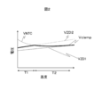
- FIG. 2 is a diagram showing the temperature characteristics of the clamp voltage according to the first embodiment.
- the horizontal axis represents temperature and the vertical axis represents voltage.
- the Zener voltage VZD2 of the second Zener diode 16 is high and the resistance value of the temperature characteristic compensating element 17 is small.
- the clamp voltage Vlamp is the sum of the Zener voltage VZD1 of the first Zener diode 15 and the voltage drop VNTC generated by the temperature characteristic compensating element 17.
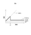
- FIG. 3 is a diagram showing the current characteristics of the clamp voltage according to the first embodiment.
- the horizontal axis represents the current flowing through the surge voltage protection circuit 10
- the vertical axis represents the voltage of the surge voltage protection circuit 10.
- Vclamp is the clamp voltage of the surge voltage protection circuit 10
- Vf is the forward voltage of the diode 14
- VZD1 is the Zener voltage of the first Zener diode 15
- VNTC is the voltage drop generated by the temperature characteristic compensation element 17
- VZD2 is the second Zener diode. It is a Zener voltage of 16.
- the Zener voltage VZD2 of the second Zener diode 16 is high and the resistance value of the temperature characteristic compensating element 17 is small, so that the current flowing through the surge voltage protection circuit 10 Flows a lot in the temperature characteristic compensating element 17. Then, when the current increases, the voltage drop VNTC generated by the temperature characteristic compensating element 17 increases, and when the second Zener diode 16 exceeds the Zener voltage VZD2 at the current I1, the second Zener diode 16 is energized. As a result, it is possible to suppress an increase in the clamp voltage V clamp when the current flowing through the surge voltage protection circuit 10 increases.
- FIG. 4 is a circuit configuration diagram of the semiconductor device 100'according to the second embodiment.
- the same parts as those of the first embodiment shown in FIG. 1 are designated by the same reference numerals, and the description thereof will be omitted.
- the surge voltage protection circuit 20 includes a diode 14, a first Zener diode 15, a first clamp voltage compensation circuit unit 20a, a second clamp voltage compensation circuit unit 20b, and so on. n It is configured by connecting in series with the clamp voltage compensation circuit unit 20n.
- the first clamp voltage compensation circuit unit 20a is composed of a second Zener diode 16a and a temperature characteristic compensation element 17a connected in parallel.
- the second clamp voltage compensation circuit unit 20b is composed of a third Zener diode 16b and a temperature characteristic compensation element 17b connected in parallel.
- the n-th clamp voltage compensation circuit unit 20n is composed of a parallel connection of the n-th Zener diode 16n and the temperature characteristic compensation element 17n.
- the temperature characteristic compensating elements 17a, 17b, ... 17n have different temperature coefficient polarities from those of the first Zener diode 15, the second Zener diode 16a, and the nth Zener diode 16n.
- the temperature at which the magnitude relationship between the Zener voltage VZD2a of the second Zener diode 16a and the voltage drop VNTCA generated by the temperature characteristic compensation element 17a in the first clamp voltage compensation circuit unit 20a changes is the second clamp voltage.
- the magnitude relationship between the Zener voltage VZD2b of the third Zener diode 16b and the voltage drop VNTCb generated by the temperature characteristic compensation element 17b in the compensation circuit unit 20b is different from the changing temperature.
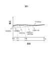
- FIG. 5 is a diagram showing the temperature characteristics of the clamp voltage according to the second embodiment.
- the horizontal axis represents temperature and the vertical axis represents voltage.
- the surge voltage protection circuit 20 is connected in series with the diode 14, the first Zener diode 15, the first clamp voltage compensation circuit section 20a, and the second clamp voltage compensation circuit section 20b. The case of being configured will be described as an example.
- the temperature characteristic compensating element 17a is more than the Zener voltage VZD2a of the second Zener diode 16a.
- the voltage drop VNTCA generated is larger.
- the voltage drop VNTCb generated by the temperature characteristic compensating element 17b is larger than the Zener voltage VZD2b of the third Zener diode 16b. Therefore, the current flowing through the surge voltage protection circuit 20 flows through the second Zener diode 16a and the third Zener diode 16b.
- the clamp voltage Vlamp is the sum of the Zener voltage VZD1 of the first Zener diode 15a, the Zener voltage VZD2a of the second Zener diode 16a, and the Zener voltage VZD2b of the third Zener diode 16b, and is calculated by the following equation (3).
- Vclamp Vf + VZD1 + VZD2a + VZD2b ...
- the temperature characteristic compensating element 17a is more than the Zener voltage VZD2a of the second Zener diode 16a.
- the voltage drop VNTCA generated is smaller.
- the voltage drop VNTCb generated by the temperature characteristic compensating element 17b is smaller than the Zener voltage VZD2b of the third Zener diode 16b. Therefore, the current flowing through the surge voltage protection circuit 20 flows through the temperature characteristic compensation element 17a and the temperature characteristic compensation element 17b.
- the clamp voltage is switched a plurality of times, so that the fluctuation of the clamp voltage is further suppressed.
- the first and second clamp voltage compensation circuit units 20a to 20b have been described, but the same applies when a plurality of clamp voltage compensation circuit units are connected in series, and fluctuations in the clamp voltage can be further suppressed.
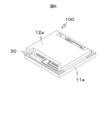
- FIG. 6 is an external view showing the mounting structure of the semiconductor device 100. This external view will be described by taking the external view of the semiconductor device 100 according to the first embodiment shown in FIG. 1 as an example, but the external view of the semiconductor device 100'according to the second embodiment shown in FIG. 4 is also shown. The same is true.
- a positive electrode side terminal conductor 11a is arranged on the lowermost surface of the substrate 30, and is composed of a conductor such as copper or aluminum having low electrical resistance and low thermal resistance.
- a negative electrode side terminal conductor 12a is arranged on the uppermost surface of the substrate 30, and is made of a conductor such as copper or aluminum.
- FIG. 7 is a diagram showing the internal structure of the semiconductor device 100, and shows a state in which the negative electrode side terminal conductor 12a shown in FIG. 6 is removed.
- a positive electrode side terminal conductor insulating layer 11b is arranged on the upper surface of the positive electrode side terminal conductor 11a, and the positive electrode side terminal conductor insulating layer 11b is made of an insulating resin, ceramic, or the like.
- a control signal layer 13a or the like is arranged on the upper surface of the positive electrode side terminal conductor insulating layer 11b, and this is made of a conductor such as copper.
- a switching element 110 is arranged on the upper surface of the positive electrode side terminal conductor 11a, and the positive electrode side terminal conductor 11a and the positive electrode side terminal 11 (see FIG. 1) of the switching element 110 are formed of a positive electrode side terminal bonding material 11d such as solder. Joined by.
- the negative electrode side terminal 12 (see FIG. 1) of the switching element 110 is joined to the negative electrode side terminal 12 (not shown) by a negative electrode side terminal bonding material 12d such as solder. At this time, the maximum output current of the semiconductor element can be increased by connecting the switching elements 110 in parallel.
- the control terminal 13 (see FIG. 1) of the switching element 110 is connected to the control signal layer 13a by a control signal line 13d such as a bonding wire, and the diode 14 constituting the surge voltage protection circuit 10 is connected to the control signal layer 13a.
- the first Zener diode 15, the second Zener diode 16, and the temperature characteristic compensation element 17 are soldered. That is, the switching element 110 and the surge voltage protection circuit 10 (diode 14, first Zener diode 15, second Zener diode 16, temperature characteristic compensation element 17) are formed on the same substrate.
- the semiconductor device 100 by arranging the first Zener diode 15, the second Zener diode 16, and the temperature characteristic compensating element 17 so as to be close to each other, the temperature variation of each component can be reduced, and the electrical characteristics can be reduced. Variation can be suppressed.
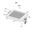
- FIG. 8 is an external view of the power module 200 incorporating the semiconductor device 100.
- the signal lines from the internal semiconductor device 100 are combined as a lower arm control signal line 13c and an upper arm control signal line 13b.
- the upper surfaces of the upper arm positive electrode side terminal 11c, the lower arm negative electrode side terminal 12c, and the upper arm negative electrode terminal / lower arm positive electrode terminal 18 are bonded to the heat radiation fin 22 by a bonding material having low thermal resistance such as solder.
- the side surface is molded with resin 21 to prevent foreign matter from entering and to improve the pressure resistance.
- FIG. 9 is a diagram showing the internal structure of the power module 200, and is a diagram showing a state in which the heat radiation fins 22 and the resin 21 shown in FIG. 8 are removed.
- FIG. 9 shows an example in which two semiconductor devices 100-1 used as the upper arm and two semiconductor devices 100-2 used as the lower arm are provided.
- the positive electrode side terminal conductor 11a (see FIG. 7) of the upper arm is connected to the positive electrode side terminal 11c of the upper arm by a bonding material such as solder.
- the negative electrode side terminal of the upper arm (see FIG. 1) and the positive electrode side terminal of the lower arm (see FIG. 1) are connected to the upper arm negative electrode terminal and the lower arm positive electrode terminal 18.
- the negative electrode side terminal of the lower arm (see FIG. 1) is connected to the lower arm negative electrode side terminal 12c.
- the upper arm positive electrode side terminal 11c and the lower arm negative electrode side terminal 12c are arranged close to each other in order to reduce the wiring inductance.
- the control terminals of the upper arm and the lower arm (see FIG. 1) are connected to the upper arm control signal line 13b and the lower arm control signal line 13c, respectively.
- the surge voltage protection circuits 10 and 20 that suppress the fluctuation of the clamp voltage can be arranged in the immediate vicinity of the switching element 110, so that the wiring inductance of the surge voltage protection circuits 10 and 20 is increased. It can be reduced and the response speed when clamping the surge voltage can be improved. Further, since the surge voltage protection circuits 10 and 20 that suppress the fluctuation of the clamp voltage do not require a control device such as a microcomputer, they can be configured in a small size and mounted inside the semiconductor device 100, 100'or the power module 200. Is possible.
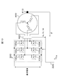
- FIG. 10 is a diagram showing a drive circuit of a motor 400 using the inverter device 300.
- the drive circuit includes an inverter device 300, an inverter control device 320, a motor 400, a position sensor 410, and a current sensor 420.
- the inverter control device 320 PWM-controls the inverter device 300 based on an external torque command T *, three-phase currents iu, iv, iwa detected by the current sensor 420, and a rotor position ⁇ detected by the position sensor 410. ..
- the inverter device 300 is composed of semiconductor devices 100a to 100f.
- Each of the semiconductor devices 100a to 100f is a semiconductor device 100 incorporating the switching element 110 and the surge voltage protection circuit 10 shown in FIG.
- each of the semiconductor devices 100a to 100f is a semiconductor device 100'in which the switching element 110 and the surge voltage protection circuit 20 shown in FIG. 4 are built.
- the semiconductor device 100a is a U-phase upper arm
- the semiconductor device 100b is a U-phase lower arm
- the semiconductor device 100c is a V-phase upper arm
- the semiconductor device 100d is a V-phase lower arm
- the semiconductor device 100e is a W-phase upper arm
- the semiconductor device 100f is W. It is placed on the lower arm.
- the switching element 110 is turned on or off based on the switching signal generated by the inverter control device 320, and the DC voltage applied from the DC power supply is converted into an AC voltage.
- the converted AC voltage is applied to the stator of the motor 400 to generate a three-phase AC current. This three-phase alternating current generates a rotating magnetic field in the motor 400, and the rotor rotates.
- the position sensor 410 detects the position of the rotor of the motor 400 and outputs the detected rotor position ⁇ to the inverter control device 320.
- the current sensor 420 detects the current flowing through the motor 400 and outputs the detected three-phase currents iu, iv, and iwa to the inverter control device 320.
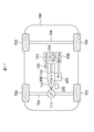
- FIG. 11 is a diagram showing a configuration of an electric vehicle.
- an inverter device 300 is mounted on a vehicle body 700 of a hybrid electric vehicle to drive a motor 400.
- the inverter device 300 includes the semiconductor device 100 or the semiconductor device 100'described in the first and second embodiments, respectively.
- the inverter device 300 operates based on the switching signal output from the inverter control device 320, and performs power conversion from DC power to AC power.
- the motor 400 is driven by using the AC power output from the inverter device 300.
- the electric vehicle runs using the driving force of the motor 400.
- the motor 400 operates not only as an electric motor that generates a rotational driving force but also as a generator that receives the driving force to generate electricity. That is, the electric vehicle is a power train to which the motor 400 is applied as a motor / generator.
- a front wheel axle 701 is rotatably supported on the front portion of the vehicle body 700, and front wheels 702 and 703 are provided at both ends of the front wheel axle 701.
- a rear wheel axle 704 is rotatably supported at the rear portion of the vehicle body 700, and rear wheels 705 and 706 are provided at both ends of the rear wheel axle 704.
- the front wheel axle 701 is provided with a differential gear 711 which is a power distribution mechanism, and distributes the rotational driving force transmitted from the engine 710 via the transmission 712 to the left and right front wheel axles 701.
- the output shaft of the engine 710 is mechanically connected to the output shaft of the motor 400 either directly or via the transmission 712. As a result, the rotational driving force of the motor 400 can be transmitted to the engine 710, and the rotational driving force of the engine 710 can be transmitted to the motor 400.
- the three-phase AC power controlled by the inverter device 300 is supplied to the stator coil of the stator, so that the rotor rotates and a rotational driving force corresponding to the three-phase AC power is generated. That is, while the motor 400 is controlled by the inverter device 300 and operates as an electric motor, an electromotive force is induced in the stator coil of the stator by the rotation of the rotor in response to the rotational driving force of the engine 710, and the three-phase AC power is generated. Operates as a generator to generate.
- the inverter device 300 converts the DC power supplied from the high-voltage battery 500, which is a DC power source of a high-voltage system (for example, 300V), into three-phase AC power, and corresponds to the magnetic pole position of the rotor according to the operation command value of the motor 400. Controls the three-phase alternating current flowing through the stator coil.
- the high-voltage battery 500 which is a DC power source of a high-voltage system (for example, 300V)
- a high-voltage system for example, 300V
- the three-phase AC power generated by the motor 400 is converted into DC power by the inverter device 300 to charge the high-voltage battery 500.
- the high voltage battery 500 is electrically connected to the low voltage battery 723 via a DC-DC converter 724.
- the low-voltage battery 723 constitutes a DC power supply for a low-voltage system (for example, 12V) of an automobile, and is used as a power source for a starter 725 that initially starts (cold start) the engine 710 and auxiliary equipment such as a radio and a light. Used.
- the inverter device 300 drives the motor 400 to drive the engine.
- Restart 710 when the charge amount of the high-voltage battery 500 is insufficient, or when the engine 710 is not sufficiently warmed up, the engine 710 may continue to be driven without stopping even in the idle stop mode. preferable. Further, in the idle stop mode, it is necessary to secure a drive source for auxiliary machinery such as an air conditioner compressor that uses the engine 710 as a drive source. In this case, the motor 400 may be driven instead of the engine 710 to serve as a drive source for auxiliary machinery.
- auxiliary machinery such as an air conditioner compressor that uses the engine 710 as a drive source.
- the motor 400 is driven to assist the driving of the engine 710.
- the engine 710 when the high-voltage battery 500 is in the charging mode that requires charging, the engine 710 generates the motor 400 to charge the high-voltage battery 500.
- the motor 400 when braking or decelerating the electric vehicle, the motor 400 may be generated by the kinetic energy of the electric vehicle to charge the high-voltage battery 500 in the regenerative mode.
- the motor 400 that generates the driving force of the vehicle body 700 is controlled by the inverter device 300, and the inverter device 300 is protected from the surge voltage by the surge voltage protection circuits 10 and 20.
- the amount of heat generated by the inverter device 300 during traveling is reduced, so that the cooling mechanism can be miniaturized, and the inverter device 300 and the radiator can be miniaturized. Further, by reducing the loss generated in the inverter device 300, the power consumption is reduced and the fuel consumption of the electric vehicle is improved.
- the switching loss generated in the inverter device 300 it is possible to increase the maximum switching frequency without improving the cooling performance of the inverter device 300.
- the frequency of the voltage ripple generated in the DC voltage section of the inverter device 300 is increased, so that the capacity of the input voltage smoothing capacitor connected in parallel with the power input terminal of the inverter device 300 can be reduced and the size can be reduced. ..
- the maximum rotation speed of the motor 400 can be improved.
- the motor 400 is downsized as it rotates at high speed, and the degree of freedom of mounting on an electric vehicle is improved, so that the space inside the vehicle can be expanded.
- the on / off controlled switching element 110 the surge voltage protection circuits 10 and 20 connected between the positive electrode side terminal of the switching element 110 and the control terminal of the switching element 110, and the surge voltage protection circuits 10 and 20
- the surge voltage protection circuits 10 and 20 include a first Zener diode 15, a second Zener diode 16 connected in series with the first Zener diode 15, and the first Zener diode 15 and the second Zener diode 16. It is composed of a temperature characteristic compensating element 17 having a different polarity of temperature coefficient and connected in parallel to the second Zener diode 16. Thereby, the variation of the clamp voltage can be suppressed regardless of the current value.
- Zener of the second Zener diode voltage the voltage drop of VNTC ⁇ ⁇ ⁇ temperature compensation element, Vclamp ⁇ ⁇ ⁇ clamp voltage, i u ⁇ ⁇ ⁇ U-phase current detection value, i v ⁇ ⁇ ⁇ V-phase current detection value, i w ⁇ ⁇ ⁇ W phase Current detection value, T * ... torque command value, ⁇ ... angular velocity, ⁇ ... rotor position.
Landscapes
- Engineering & Computer Science (AREA)
- Power Engineering (AREA)
- Inverter Devices (AREA)
- Power Conversion In General (AREA)
Abstract
サーミスタを流れる電流値が大きくなった場合に、サーミスタで発生する電圧降下が増大し、クランプ電圧にばらつきが発生する課題があった。 オンオフ制御されるスイッチング素子と、前記スイッチング素子の正極側端子と前記スイッチング素子の制御端子との間に接続されるサージ電圧保護回路と、を備え、前記サージ電圧保護回路は、第1ツェナーダイオードと、前記第1ツェナーダイオードと直列に接続される第2ツェナーダイオードと、前記第1ツェナーダイオードおよび前記第2ツェナーダイオードとは温度係数の極性が異なり、かつ前記第2ツェナーダイオードに並列に接続される温度特性補償素子と、により構成される半導体装置。
Description
本発明は、半導体装置、パワーモジュール、インバータ装置、および電動車両に関する。
ハイブリッド自動車や電気自動車などの電動車両に搭載されるインバータ装置には、オンオフ制御されるスイッチング素子が用いられる。このスイッチング素子は、スイッチング時間の短縮とサージ電圧の抑制の両立が望まれる。そのため、スイッチング素子の正極側端子とスイッチング素子の制御端子との間にサージ電圧保護回路が設けられている。サージ電圧保護回路は、スイッチング素子のドレイン・ソース間のブレークダウン電圧よりも低い電圧(クランプ電圧)で動作するように設定されており、サージが発生すると、スイッチング素子より先にブレークダウンしてスイッチング素子を保護する。
特許文献1には、ツェナーダイオードZ1のカソードがMOSFETのドレインに接続され、ダイオードのアノードがツェナーダイオードZ1のアノードに接続され、サーミスタがダイオードのカソードとMOSFETのゲート間に接続され、サーミスタに固定抵抗器が並列に接続された負荷制御装置が開示されている。
特許文献1に記載の装置では、サーミスタを流れる電流値が大きくなった場合に、サーミスタで発生する電圧降下が増大し、クランプ電圧にばらつきが発生する課題があった。
本発明による半導体装置は、オンオフ制御されるスイッチング素子と、前記スイッチング素子の正極側端子と前記スイッチング素子の制御端子との間に接続されるサージ電圧保護回路と、を備え、前記サージ電圧保護回路は、第1ツェナーダイオードと、前記第1ツェナーダイオードと直列に接続される第2ツェナーダイオードと、前記第1ツェナーダイオードおよび前記第2ツェナーダイオードとは温度係数の極性が異なり、かつ前記第2ツェナーダイオードに並列に接続される温度特性補償素子と、により構成される。
本発明によれば、電流値に因らずクランプ電圧のばらつきを抑制することができる。
[第1の実施形態] 以下、図面を参照して本発明の実施形態を説明する。ただし、本発明は下記の実施形態に限定解釈されるものではなく、公知の他の構成要素を組み合わせて本発明の技術思想を実現してもよい。なお、各図において同一要素については同一の符号を記し、重複する説明は省略する。
図1は、本実施形態に係る半導体装置100の回路構成図である。
スイッチング素子110は、金属酸化膜型電界効果トランジスタ(MOSFET)や、絶縁ゲートバイポーラトランジスタ(IGBT)とダイオードの組み合わせなどで構成され、正極側端子11と、負極側端子12と、制御端子13を備える。
スイッチング素子110は、金属酸化膜型電界効果トランジスタ(MOSFET)や、絶縁ゲートバイポーラトランジスタ(IGBT)とダイオードの組み合わせなどで構成され、正極側端子11と、負極側端子12と、制御端子13を備える。
正極側端子11は図示していないインバータ装置の正極側に、負極側端子12は図示していないインバータ装置の負極側に、制御端子13は図示していないインバータ制御装置に接続されている。スイッチング素子110は、制御端子13に入力される制御信号に基づいて正極側端子11から負極側端子12に流れる電流のオンとオフが制御される。
サージ電圧保護回路10は、スイッチング素子110の正極側端子11とスイッチング素子110の制御端子13の間に接続されている。一般に、サージ電圧保護回路10は、ダイオード14と第1ツェナーダイオード15が直列に接続されて構成されている。この構成において、スイッチング素子110のスイッチングによって正極側端子11と負極側端子12の間に発生するサージ電圧が第1ツェナーダイオード15のツェナー電圧によって設定されるクランプ電圧を超過したとする。この際に、第1ツェナーダイオード15が通電することによって正極側端子11から制御端子13へ電流が流れて、制御端子13の電位を上昇させることでスイッチング素子110をサージ電圧から保護している。
本実施形態においては、サージ電圧保護回路10は、図1に示すように、ダイオード14と、第1ツェナーダイオード15と、第1ツェナーダイオード15と直列に接続される第2ツェナーダイオード16と、第1ツェナーダイオード15および第2ツェナーダイオード16とは温度係数の極性が異なり、かつ第2ツェナーダイオード16に並列に接続される温度特性補償素子17と、により構成される。温度特性補償素子17は、例えばサーミスタである。
温度特性補償素子17は、第2ツェナーダイオード16と温度係数の極性が異なり、第2ツェナーダイオード16が正の温度係数を有する場合、温度特性補償素子17は負の温度係数を有する。すなわち、第2ツェナーダイオード16および温度特性補償素子17の素子温度が上昇した場合、第2ツェナーダイオード16のツェナー電圧は上昇するが、温度特性補償素子17の抵抗値は低下する。一方、第2ツェナーダイオード16および温度特性補償素子17の素子温度が低下した場合、第2ツェナーダイオード16のツェナー電圧は低下するが、温度特性補償素子17の抵抗値は上昇する。その結果、第2ツェナーダイオード16および温度特性補償素子17の素子温度が高い場合、サージ電圧保護回路10を流れる電流は温度特性補償素子17に多く流れ、第2ツェナーダイオード16および温度特性補償素子17の素子温度が低い場合、サージ電圧保護回路10を流れる電流は第2ツェナーダイオード16に多く流れる。
したがって、第2ツェナーダイオード16および温度特性補償素子17の素子温度が高い場合のクランプ電圧は次式(1)によって算出され、第2ツェナーダイオード16および温度特性補償素子17の素子温度が低い場合のクランプ電圧は次式(2)によって算出される。
Vclamp=Vf+VZD1+VNTC・・・(1)
Vclamp=Vf+VZD1+VZD2・・・(2)
ここでVclampはサージ電圧保護回路10のクランプ電圧、Vfはダイオード14の順方向電圧、VZD1は第1ツェナーダイオード15のツェナー電圧、VNTCは温度特性補償素子17で発生する電圧降下、VZD2は第2ツェナーダイオード16のツェナー電圧である。
Vclamp=Vf+VZD1+VNTC・・・(1)
Vclamp=Vf+VZD1+VZD2・・・(2)
ここでVclampはサージ電圧保護回路10のクランプ電圧、Vfはダイオード14の順方向電圧、VZD1は第1ツェナーダイオード15のツェナー電圧、VNTCは温度特性補償素子17で発生する電圧降下、VZD2は第2ツェナーダイオード16のツェナー電圧である。
図2は、第1の実施形態に係るクランプ電圧の温度特性を示す図である。図2において、横軸は温度を、縦軸は電圧を示す。
第2ツェナーダイオード16および温度特性補償素子17の温度が低い場合(図2のT1)、第2ツェナーダイオード16のツェナー電圧VZD2は低く、温度特性補償素子17の抵抗値は大きいため、クランプ電圧Vclampは(2)式に示した通り、第1ツェナーダイオード15のツェナー電圧VZD1と第2ツェナーダイオード16のツェナー電圧VZD2の和となる。
一方、第2ツェナーダイオード16および温度特性補償素子17の素子温度が高い場合(図2のT2)、第2ツェナーダイオード16のツェナー電圧VZD2は高く、温度特性補償素子17の抵抗値は小さいため、クランプ電圧Vclampは(1)式に示した通り、第1ツェナーダイオード15のツェナー電圧VZD1と温度特性補償素子17で発生する電圧降下VNTCの和となる。この結果、第1ツェナーダイオード15のみを用いた一般の構成と比較して、温度変化に伴うクランプ電圧の変動が抑制される。
図3は、第1の実施形態に係るクランプ電圧の電流特性を示す図である。図3において、横軸はサージ電圧保護回路10を流れる電流を、縦軸はサージ電圧保護回路10の電圧を示す。Vclampはサージ電圧保護回路10のクランプ電圧、Vfはダイオード14の順方向電圧、VZD1は第1ツェナーダイオード15のツェナー電圧、VNTCは温度特性補償素子17で発生する電圧降下、VZD2は第2ツェナーダイオード16のツェナー電圧である。
第2ツェナーダイオード16および温度特性補償素子17の素子温度が高い場合、第2ツェナーダイオード16のツェナー電圧VZD2は高く、温度特性補償素子17の抵抗値は小さいため、サージ電圧保護回路10を流れる電流は温度特性補償素子17に多く流れる。そして、その電流が増加した場合、温度特性補償素子17で発生する電圧降下VNTCが増大し、電流I1において、第2ツェナーダイオード16がツェナー電圧VZD2を超過すると第2ツェナーダイオード16が通電する。これにより、サージ電圧保護回路10を流れる電流が増加した際にクランプ電圧Vclampが増大することを抑制することができる。
[第2の実施形態] 図4は第2の実施形態に係る半導体装置100’の回路構成図である。図1に示した第1の実施形態と同一の個所には同一の符号を附してその説明を省略する。
第2の実施形態においては、サージ電圧保護回路20は、ダイオード14と、第1ツェナーダイオード15と、第1クランプ電圧補償回路部20aと、第2クランプ電圧補償回路部20bと、・・・第nクランプ電圧補償回路部20nとの直列接続により構成される。
第1クランプ電圧補償回路部20aは、第2ツェナーダイオード16aと温度特性補償素子17aの並列接続で構成される。第2クランプ電圧補償回路部20bは、第3ツェナーダイオード16bと温度特性補償素子17bの並列接続で構成される。第nクランプ電圧補償回路部20nは、第nツェナーダイオード16nと温度特性補償素子17nの並列接続で構成される。温度特性補償素子17a、17b、・・17nは、第1ツェナーダイオード15、第2ツェナーダイオード16a、および第nツェナーダイオード16nとは温度係数の極性が異なる。
第2の実施形態では、第1クランプ電圧補償回路部20aにおける第2ツェナーダイオード16aのツェナー電圧VZD2aと温度特性補償素子17aで発生する電圧降下VNTCaの大小関係が変化する温度は、第2クランプ電圧補償回路部20bにおける第3ツェナーダイオード16bのツェナー電圧VZD2bと温度特性補償素子17bで発生する電圧降下VNTCbの大小関係が変化する温度と異なる。
図5は、第2の実施形態に係るクランプ電圧の温度特性を示す図である。図2において、横軸は温度を、縦軸は電圧を示す。
以下、説明を簡単にするため、サージ電圧保護回路20が、ダイオード14と、第1ツェナーダイオード15と、第1クランプ電圧補償回路部20aと、第2クランプ電圧補償回路部20bとの直列接続により構成される場合を例に説明する。
以下、説明を簡単にするため、サージ電圧保護回路20が、ダイオード14と、第1ツェナーダイオード15と、第1クランプ電圧補償回路部20aと、第2クランプ電圧補償回路部20bとの直列接続により構成される場合を例に説明する。
第1~第2クランプ電圧補償回路部20a~20bの部品温度が、図5に示すように、T0~T1の低温時は、第2ツェナーダイオード16aのツェナー電圧VZD2aよりも温度特性補償素子17aで発生する電圧降下VNTCaのほうが大きい。また、第3ツェナーダイオード16bのツェナー電圧VZD2bよりも温度特性補償素子17bで発生する電圧降下VNTCbのほうが大きい。このため、サージ電圧保護回路20を流れる電流は、第2ツェナーダイオード16aと第3ツェナーダイオード16bを流れる。したがって、クランプ電圧Vclampは第1ツェナーダイオード15aのツェナー電圧VZD1と第2ツェナーダイオード16aのツェナー電圧VZD2aと第3ツェナーダイオード16bのツェナー電圧VZD2bの和となり、次式(3)によって算出される。
Vclamp=Vf+VZD1+VZD2a+VZD2b・・・(3)
Vclamp=Vf+VZD1+VZD2a+VZD2b・・・(3)
第1~第2クランプ電圧補償回路部20a~20bの部品温度が、図5に示すように、T1~T2に上昇すると、第2ツェナーダイオード16aのツェナー電圧VZD2aよりも温度特性補償素子17aで発生する電圧降下VNTCaのほうが大きい。また、第3ツェナーダイオード16bのツェナー電圧VZD2bよりも温度特性補償素子17bで発生する電圧降下VNTCbのほうが小さい。このため、サージ電圧保護回路20を流れる電流は、第2ツェナーダイオード16aと温度特性補償素子17bを流れる。したがって、クランプ電圧Vclampは第1ツェナーダイオード15aのツェナー電圧VZD1と第2ツェナーダイオード16aのツェナー電圧VZD2aと温度特性補償素子17bで発生する電圧降下VNTCbの和となり、次式(4)によって算出される。
Vclamp=Vf+VZD1+VZD2a+VNTCb・・・(4)
Vclamp=Vf+VZD1+VZD2a+VNTCb・・・(4)
第1~第2クランプ電圧補償回路部20a~20bの部品温度が、図5に示すように、T2~T3の高温時は、第2ツェナーダイオード16aのツェナー電圧VZD2aよりも温度特性補償素子17aで発生する電圧降下VNTCaのほうが小さい。また、第3ツェナーダイオード16bのツェナー電圧VZD2bよりも温度特性補償素子17bで発生する電圧降下VNTCbのほうが小さい。このため、サージ電圧保護回路20を流れる電流は、温度特性補償素子17aと温度特性補償素子17bを流れる。したがって、クランプ電圧Vclampは第1ツェナーダイオード15aのツェナー電圧VZD1aと温度特性補償素子17aで発生する電圧降下VNTCaと温度特性補償素子17bで発生する電圧降下VNTCbの和となり、次式(5)によって算出される。
Vclamp=Vf+VZD1+VNTCa+VNTCb・・・(5)
Vclamp=Vf+VZD1+VNTCa+VNTCb・・・(5)
その結果、第1~第2クランプ電圧補償回路部20a~20bの部品温度が変化した際にクランプ電圧が複数回切り替わるためクランプ電圧の変動がさらに抑制される。第1~第2クランプ電圧補償回路部20a~20bについて説明したが、複数のクランプ電圧補償回路部が直列接続された場合も同様であり、クランプ電圧の変動をさらに抑制することができる。
図6は、半導体装置100の実装構造を示す外観図である。この外観図は、図1で示した第1の実施形態に係る半導体装置100の外観図を例に説明するが、図4で示した第2の実施形態に係る半導体装置100’の外観図も同様である。
基板30の最下面には正極側端子導体11aが配置され、銅やアルミニウムなど電気抵抗が小さく熱抵抗も小さい導体により構成されている。基板30の最上面には負極側端子導体12aが配置され、銅やアルミニウムなどの導体により構成されている。
図7は、半導体装置100の内部構造を示す図であり、図6に示す負極側端子導体12aを取り除いた状態の図を示す。
正極側端子導体11aの上面には正極側端子導体絶縁層11bが配置されており、正極側端子導体絶縁層11bは絶縁性の樹脂やセラミックなどにより構成されている。正極側端子導体絶縁層11bの上面には制御信号層13aなどが配置されており、これは銅などの導体により構成されている。また、正極側端子導体11aの上面にはスイッチング素子110が配置されており、正極側端子導体11aとスイッチング素子110の正極側端子11(図1参照)は、はんだなどの正極側端子接合材11dによって接合されている。一方、スイッチング素子110の負極側端子12(図1参照)は、はんだなどの負極側端子接合材12dによって図示されていない負極側端子12に接合されている。このとき、スイッチング素子110を多並列接続することによって、半導体素子の最大出力電流を増加させることができる。
スイッチング素子110の制御端子13(図1参照)は、ボンディングワイヤなどの制御信号線13dによって制御信号層13aに接続されており、制御信号層13aにはサージ電圧保護回路10を構成するダイオード14、第1ツェナーダイオード15、第2ツェナーダイオード16、温度特性補償素子17がはんだ付けされている。すなわち、スイッチング素子110とサージ電圧保護回路10(ダイオード14、第1ツェナーダイオード15、第2ツェナーダイオード16、温度特性補償素子17)とは、同一の基板上に形成されている。このとき、半導体装置100において、第1ツェナーダイオード15と第2ツェナーダイオード16と温度特性補償素子17がそれぞれ近接するように配置することによって各部品の温度のばらつきを低減することができ、電気特性のばらつきを抑制することができる。
図8は、半導体装置100を内蔵したパワーモジュール200の外観図である。
内部の半導体装置100からの信号線は下アーム制御信号線13cと上アーム制御信号線13bとしてまとめられる。上アーム正極側端子11cと下アーム負極側端子12c、および上アーム負極端子・下アーム正極端子18の上面ははんだなど熱抵抗の小さい接合材料によって放熱フィン22に接合されている。側面は樹脂21によってモールドすることで異物の混入を防ぎ、また耐圧の向上を計っている。
内部の半導体装置100からの信号線は下アーム制御信号線13cと上アーム制御信号線13bとしてまとめられる。上アーム正極側端子11cと下アーム負極側端子12c、および上アーム負極端子・下アーム正極端子18の上面ははんだなど熱抵抗の小さい接合材料によって放熱フィン22に接合されている。側面は樹脂21によってモールドすることで異物の混入を防ぎ、また耐圧の向上を計っている。
図9は、パワーモジュール200の内部構造を示す図であり、図8に示す放熱フィン22や樹脂21を取り除いた状態を示す図である。
図9では、上アームとして用いる半導体装置100-1を2個、下アームとして用いる半導体装置100-2を2個設けた例を示す。上アームの正極側端子導体11a(図7参照)ははんだなどの接合材によって上アーム正極側端子11cに接続される。上アームの負極側端子(図1参照)および下アームの正極側端子(図1参照)は上アーム負極端子・下アーム正極端子18に接続される。下アームの負極側端子(図1参照)は下アーム負極側端子12cに接続される。配線インダクタンスを低減するために上アーム正極側端子11cと下アーム負極側端子12cは近接して配置される。上アームおよび下アームの制御端子(図1参照)はそれぞれ上アーム制御信号線13b、下アーム制御信号線13cに接続される。
第1および第2の実施形態においては、クランプ電圧の変動を抑制するサージ電圧保護回路10、20をスイッチング素子110の直近に配置することができるため、サージ電圧保護回路10、20の配線インダクタンスを低減することが可能となり、サージ電圧をクランプする際の応答速度を向上させることができる。また、クランプ電圧の変動を抑制するサージ電圧保護回路10、20にマイコンなどの制御装置を必要しないため、小型に構成することができ半導体装置100、100’若しくはパワーモジュール200の内部に搭載することが可能となる。
図10は、インバータ装置300を用いたモータ400の駆動回路を示す図である。
駆動回路は、インバータ装置300と、インバータ制御装置320と、モータ400と、位置センサ410と、電流センサ420と、を備える。
駆動回路は、インバータ装置300と、インバータ制御装置320と、モータ400と、位置センサ410と、電流センサ420と、を備える。
インバータ制御装置320は外部からのトルク指令T*、電流センサ420で検出された三相電流iu、iv、iw、位置センサ410で検出された回転子位置θに基づいてインバータ装置300をPWM制御する。
インバータ装置300は、半導体装置100a~100fにより構成される。各半導体装置100a~100fは、図1で示したスイッチング素子110およびサージ電圧保護回路10を内蔵する半導体装置100である。もしくは、各半導体装置100a~100fは、図4で示したスイッチング素子110およびサージ電圧保護回路20を内蔵する半導体装置100’である。
半導体装置100aはU相上アーム、半導体装置100bはU相下アーム、半導体装置100cはV相上アーム、半導体装置100dはV相下アーム、半導体装置100eはW相上アーム、半導体装置100fはW相下アームに配置される。
半導体装置100a~100fは、インバータ制御装置320で生成されたスイッチング信号に基づいてスイッチング素子110がオンもしくはオフされ、直流電源から印加された直流電圧を交流電圧に変換する。変換された交流電圧は、モータ400の固定子に印加され、3相交流電流を発生させる。この3相交流電流がモータ400に回転磁界を発生させ、回転子が回転する。
位置センサ410は、モータ400の回転子の位置を検出し、検出した回転子位置θをインバータ制御装置320へ出力する。電流センサ420は、モータ400に流れる電流を検出し、検出した三相電流iu、iv、iwをインバータ制御装置320へ出力する。
図11は、電動車両の構成を示す図である。
図11に示す電動車両は、ハイブリッド電気自動車の車体700にインバータ装置300を搭載し、モータ400を駆動する。インバータ装置300は、第1および第2の実施形態でそれぞれ説明した半導体装置100、もしくは半導体装置100’を有している。
図11に示す電動車両は、ハイブリッド電気自動車の車体700にインバータ装置300を搭載し、モータ400を駆動する。インバータ装置300は、第1および第2の実施形態でそれぞれ説明した半導体装置100、もしくは半導体装置100’を有している。
インバータ装置300は、インバータ制御装置320から出力されるスイッチング信号に基づいて動作し、直流電力から交流電力への電力変換を行う。モータ400は、インバータ装置300から出力される交流電力を用いて駆動する。これにより、モータ400の駆動力を用いて電動車両が走行する。さらに、モータ400は回転駆動力を発生する電動機としてだけでなく、駆動力を受けて発電する発電機として動作する。すなわち、電動車両は、モータ400をモータ/ジェネレータとして適用したパワートレインである。
車体700のフロント部には、前輪車軸701が回転可能に軸支されており、前輪車軸701の両端には、前輪702、703が設けられている。車体700のリア部には、後輪車軸704が回転可能に軸支されており、後輪車軸704の両端には後輪705、706が設けられている。前輪車軸701には、動力分配機構であるデファレンシャルギア711が設けられており、エンジン710から変速機712を介して伝達された回転駆動力を左右の前輪車軸701に分配する。
エンジン710の出力軸は、モータ400の出力軸に直接または変速機712を介して機械的に連結されている。これにより、モータ400の回転駆動力がエンジン710に、エンジン710の回転駆動力がモータ400にそれぞれ伝達できるようになっている。
モータ400は、インバータ装置300によって制御された三相交流電力がステータのステータコイルに供給されることによって、ロータが回転し、三相交流電力に応じた回転駆動力を発生する。すなわち、モータ400は、インバータ装置300によって制御されて電動機として動作する一方、エンジン710の回転駆動力を受けてロータが回転することによって、ステータのステータコイルに起電力が誘起され、三相交流電力を発生する発電機として動作する。
インバータ装置300は、高電圧系(例えば300V)の直流電源である高圧バッテリ500から供給された直流電力を三相交流電力に変換し、運転指令値に従ってロータの磁極位置に応じた、モータ400のステータコイルに流れる三相交流電流を制御する。
モータ400によって発電された三相交流電力は、インバータ装置300によって直流電力に変換されて高圧バッテリ500を充電する。高圧バッテリ500はDC-DCコンバータ724を介して低圧バッテリ723に電気的に接続されている。低圧バッテリ723は、自動車の低電圧系(例えば12V)の直流電源を構成するものであり、エンジン710を初期始動(コールド始動)させるスタータ725や、ラジオ、ライト等の補機類などの電源に用いられる。
電動車両が信号待ちなどの停車時(アイドルストップモード)にあるとき、エンジン710を停止させ、再発車時にエンジン710を再始動(ホット始動)させる時には、インバータ装置300でモータ400を駆動し、エンジン710を再始動させる。ただし、高圧バッテリ500の充電量が不足している場合や、エンジン710が十分に温まっていない場合などにおいては、アイドルストップモードであっても、エンジン710を停止せずに駆動を継続することが好ましい。また、アイドルストップモード中においては、エアコンのコンプレッサなど、エンジン710を駆動源としている補機類の駆動源を確保する必要がある。この場合、エンジン710の代わりにモータ400を駆動させて補機類の駆動源としてもよい。
一方、電動車両が加速モードや高負荷運転モードにあるときは、モータ400を駆動させてエンジン710の駆動をアシストする。逆に、高圧バッテリ500の充電が必要な充電モードにあるときは、エンジン710によってモータ400を発電させて高圧バッテリ500を充電する。さらに、電動車両の制動時や減速時などには回生モードとして、電動車両の運動エネルギーによりモータ400を発電させて高圧バッテリ500を充電してもよい。
本実施形態に係る電動車両においては、車体700の駆動力を発生させるモータ400はインバータ装置300によって制御されており、インバータ装置300はサージ電圧保護回路10、20によってサージ電圧から保護されている。
したがって、サージ電圧保護回路10、20の温度変化に伴うクランプ電圧Vclampの変動は第2ツェナーダイオード16および温度特性補償素子17等によって抑制されているため、サージ電圧保護回路10、20を設計する際にスイッチング素子110の素子耐圧に対するクランプ電圧のマージンを低減することが可能となる。そのためサージ電圧保護回路10、20の部品温度によらずスイッチング素子110の素子耐圧に対して適正なマージンが確保されたクランプ電圧でスイッチング素子110が動作するため、スイッチング時間が短縮されてスイッチング損失が低減される。
その結果、走行時にインバータ装置300で発生する発熱量が低減されるため冷却機構の小型化が可能となり、インバータ装置300およびラジエターの小型化が可能となる。さらにインバータ装置300で発生する損失が低減することによって消費電力量が低減され、電動車両の燃費が向上する。
また、インバータ装置300で発生するスイッチング損失が低減されることにより、インバータ装置300の冷却性能を向上させることなく最大スイッチング周波数を高周波化することが可能となる。これによりインバータ装置300の直流電圧部に発生する電圧リプルの周波数が高周波化されるため、インバータ装置300の電源入力端子と並列に接続される入力電圧平滑コンデンサの容量削減および小型化が可能となる。さらにインバータ装置300の最大出力周波数を向上させることができるため、モータ400の最高回転数を向上させることが可能となる。その結果、モータ400が高速回転化に伴い小型化され、電動車両への搭載自由度が向上することで車内空間の拡大が可能となる。
以上説明した実施形態によれば、次の作用効果が得られる。
(1)半導体装置100、100’は、オンオフ制御されるスイッチング素子110と、スイッチング素子110の正極側端子とスイッチング素子110の制御端子との間に接続されるサージ電圧保護回路10、20と、を備え、サージ電圧保護回路10、20は、第1ツェナーダイオード15と、第1ツェナーダイオード15と直列に接続される第2ツェナーダイオード16と、第1ツェナーダイオード15および第2ツェナーダイオード16とは温度係数の極性が異なり、かつ第2ツェナーダイオード16に並列に接続される温度特性補償素子17と、により構成される。これにより、電流値に因らずクランプ電圧のばらつきを抑制することができる。
(1)半導体装置100、100’は、オンオフ制御されるスイッチング素子110と、スイッチング素子110の正極側端子とスイッチング素子110の制御端子との間に接続されるサージ電圧保護回路10、20と、を備え、サージ電圧保護回路10、20は、第1ツェナーダイオード15と、第1ツェナーダイオード15と直列に接続される第2ツェナーダイオード16と、第1ツェナーダイオード15および第2ツェナーダイオード16とは温度係数の極性が異なり、かつ第2ツェナーダイオード16に並列に接続される温度特性補償素子17と、により構成される。これにより、電流値に因らずクランプ電圧のばらつきを抑制することができる。
本発明は、上記の実施形態に限定されるものではなく、本発明の特徴を損なわない限り、本発明の技術思想の範囲内で考えられるその他の形態についても、本発明の範囲内に含まれる。
10、20・・・サージ電圧保護回路、11・・・正極側端子、12・・・負極側端子、13・・・制御端子、14・・・ダイオード、15・・・第1ツェナーダイオード、16・・・第2ツェナーダイオード、17・・・温度特性補償素子、21・・・樹脂、22・・・放熱フィン、100、100’・・・半導体装置、100a・・・U相上アーム半導体装置、100b・・・U相下アーム半導体装置、100c・・・V相上アーム半導体装置、100d・・・V相下アーム半導体装置、100e・・・W相上アーム半導体装置、100f・・・W相下アーム半導体装置、110・・・スイッチング素子、300・・・インバータ装置、320・・・インバータ制御装置、400・・・モータ、410・・・位置センサ、420・・・電流センサ、700・・・車体、701・・・前輪車軸、702、703・・・前輪、704・・・後輪車軸、705、706・・・後輪、710・・・エンジン、711・・・デファレンシャルギア、712・・・変速機、723・・・低圧バッテリ、724・・・DC-DCコンバータ、725・・・スタータ、VZD1・・・第1ツェナーダイオードのツェナー電圧、VZD2・・・第2ツェナーダイオードのツェナー電圧、VNTC・・・温度特性補償素子の電圧降下、Vclamp・・・クランプ電圧、iu・・・U相電流検出値、iv・・・V相電流検出値、iw・・・W相電流検出値、T*・・・トルク指令値、ω・・・角速度、θ・・・回転子位置。
Claims (7)
- オンオフ制御されるスイッチング素子と、
前記スイッチング素子の正極側端子と前記スイッチング素子の制御端子との間に接続されるサージ電圧保護回路と、を備え、
前記サージ電圧保護回路は、第1ツェナーダイオードと、前記第1ツェナーダイオードと直列に接続される第2ツェナーダイオードと、前記第1ツェナーダイオードおよび前記第2ツェナーダイオードとは温度係数の極性が異なり、かつ前記第2ツェナーダイオードに並列に接続される温度特性補償素子と、により構成される半導体装置。 - 請求項1に記載の半導体装置において、
前記サージ電圧保護回路は、前記第2ツェナーダイオードとツェナー電圧が異なり、かつ前記第2ツェナーダイオードに対して直列に接続される複数のツェナーダイオードと、 前記第1ツェナーダイオード、前記第2ツェナーダイオード、および前記複数のツェナーダイオードとは温度係数の極性が異なり、かつ前記複数の各ツェナーダイオードと並列に接続される温度特性補償素子と、により構成される半導体装置。 - 請求項1に記載の半導体装置において、
前記第2ツェナーダイオードのツェナー電圧は前記第1ツェナーダイオードのツェナー電圧よりも低い半導体装置。 - 請求項1に記載の半導体装置において、
前記温度特性補償素子はサーミスタである半導体装置。 - 請求項1から請求項4までの何れか一項に記載の半導体装置を備え、
前記スイッチング素子と前記サージ電圧保護回路とを同一の基板上に形成したパワーモジュール。 - 請求項5に記載のパワーモジュールを備え、直流電圧を交流電圧に変換するインバータ装置。
- 請求項6に記載のインバータ装置を備え、前記交流電圧によりモータを駆動する電動車両。
Priority Applications (3)
| Application Number | Priority Date | Filing Date | Title |
|---|---|---|---|
| DE112021000359.3T DE112021000359T5 (de) | 2020-03-23 | 2021-01-15 | Halbleitervorrichtung, leistungsmodul, wechselrichtervorrichtung, und elektrisches fahrzeug |
| US17/911,962 US12501714B2 (en) | 2020-03-23 | 2021-01-15 | Semiconductor device, power module, inverter device, and electric vehicle |
| CN202180014860.9A CN115136477B (zh) | 2020-03-23 | 2021-01-15 | 半导体装置、功率模块、逆变器装置以及电动车辆 |
Applications Claiming Priority (2)
| Application Number | Priority Date | Filing Date | Title |
|---|---|---|---|
| JP2020051598A JP7232788B2 (ja) | 2020-03-23 | 2020-03-23 | 半導体装置、パワーモジュール、インバータ装置、および電動車両 |
| JP2020-051598 | 2020-03-23 |
Publications (1)
| Publication Number | Publication Date |
|---|---|
| WO2021192530A1 true WO2021192530A1 (ja) | 2021-09-30 |
Family
ID=77849747
Family Applications (1)
| Application Number | Title | Priority Date | Filing Date |
|---|---|---|---|
| PCT/JP2021/001184 Ceased WO2021192530A1 (ja) | 2020-03-23 | 2021-01-15 | 半導体装置、パワーモジュール、インバータ装置、および電動車両 |
Country Status (5)
| Country | Link |
|---|---|
| US (1) | US12501714B2 (ja) |
| JP (1) | JP7232788B2 (ja) |
| CN (1) | CN115136477B (ja) |
| DE (1) | DE112021000359T5 (ja) |
| WO (1) | WO2021192530A1 (ja) |
Cited By (1)
| Publication number | Priority date | Publication date | Assignee | Title |
|---|---|---|---|---|
| JPWO2025196919A1 (ja) * | 2024-03-18 | 2025-09-25 |
Citations (5)
| Publication number | Priority date | Publication date | Assignee | Title |
|---|---|---|---|---|
| JPS6015720A (ja) * | 1983-07-06 | 1985-01-26 | Hitachi Lighting Ltd | 低温補償形位相制御回路 |
| JPH09163583A (ja) * | 1995-11-30 | 1997-06-20 | Mitsubishi Electric Corp | 半導体素子の保護回路 |
| JP2004247877A (ja) * | 2003-02-12 | 2004-09-02 | Denso Corp | 誘導性負荷駆動用ic、その使用方法及び電子装置 |
| JP2009540631A (ja) * | 2006-06-02 | 2009-11-19 | フリースケール セミコンダクター インコーポレイテッド | 誘導性フライバックが発生している状態の過渡電圧を低減したパワートランジスタのスルーレート制御装置及び方法 |
| JP2019047416A (ja) * | 2017-09-06 | 2019-03-22 | 日立オートモティブシステムズ株式会社 | 負荷制御装置 |
Family Cites Families (10)
| Publication number | Priority date | Publication date | Assignee | Title |
|---|---|---|---|---|
| JP3598933B2 (ja) * | 2000-02-28 | 2004-12-08 | 株式会社日立製作所 | 電力変換装置 |
| JP3979096B2 (ja) | 2002-01-22 | 2007-09-19 | 株式会社日立製作所 | 半導体素子の駆動装置ならびにそれを用いた電力変換装置 |
| US7742270B2 (en) * | 2004-06-10 | 2010-06-22 | Invensys Systems, Inc. | System and method for limiting energy in an industrial control system |
| DE102005019709A1 (de) | 2005-04-28 | 2006-11-02 | Robert Bosch Gmbh | Endstufe mit Zenerspannungs-Symmetrierung |
| DE102005051004A1 (de) * | 2005-10-25 | 2007-04-26 | Robert Bosch Gmbh | Temperaturkompensation bei Endstufen |
| US20090273868A1 (en) * | 2008-05-01 | 2009-11-05 | Semiconductor Components Industries, Llc | Transient voltage suppressor and method |
| JP2011024382A (ja) * | 2009-07-17 | 2011-02-03 | Fuji Electric Systems Co Ltd | ゲート駆動回路 |
| JP6962219B2 (ja) | 2018-01-31 | 2021-11-05 | 株式会社アイシン | インバータ保護回路 |
| JP7052452B2 (ja) * | 2018-03-19 | 2022-04-12 | 富士電機株式会社 | 半導体装置 |
| CN110798056A (zh) * | 2018-08-03 | 2020-02-14 | 欧姆龙株式会社 | 电源电路 |
-
2020
- 2020-03-23 JP JP2020051598A patent/JP7232788B2/ja active Active
-
2021
- 2021-01-15 DE DE112021000359.3T patent/DE112021000359T5/de active Pending
- 2021-01-15 US US17/911,962 patent/US12501714B2/en active Active
- 2021-01-15 CN CN202180014860.9A patent/CN115136477B/zh active Active
- 2021-01-15 WO PCT/JP2021/001184 patent/WO2021192530A1/ja not_active Ceased
Patent Citations (5)
| Publication number | Priority date | Publication date | Assignee | Title |
|---|---|---|---|---|
| JPS6015720A (ja) * | 1983-07-06 | 1985-01-26 | Hitachi Lighting Ltd | 低温補償形位相制御回路 |
| JPH09163583A (ja) * | 1995-11-30 | 1997-06-20 | Mitsubishi Electric Corp | 半導体素子の保護回路 |
| JP2004247877A (ja) * | 2003-02-12 | 2004-09-02 | Denso Corp | 誘導性負荷駆動用ic、その使用方法及び電子装置 |
| JP2009540631A (ja) * | 2006-06-02 | 2009-11-19 | フリースケール セミコンダクター インコーポレイテッド | 誘導性フライバックが発生している状態の過渡電圧を低減したパワートランジスタのスルーレート制御装置及び方法 |
| JP2019047416A (ja) * | 2017-09-06 | 2019-03-22 | 日立オートモティブシステムズ株式会社 | 負荷制御装置 |
Cited By (1)
| Publication number | Priority date | Publication date | Assignee | Title |
|---|---|---|---|---|
| JPWO2025196919A1 (ja) * | 2024-03-18 | 2025-09-25 |
Also Published As
| Publication number | Publication date |
|---|---|
| US12501714B2 (en) | 2025-12-16 |
| DE112021000359T5 (de) | 2022-12-08 |
| US20230148137A1 (en) | 2023-05-11 |
| CN115136477A (zh) | 2022-09-30 |
| CN115136477B (zh) | 2026-06-02 |
| JP2021151159A (ja) | 2021-09-27 |
| JP7232788B2 (ja) | 2023-03-03 |
Similar Documents
| Publication | Publication Date | Title |
|---|---|---|
| CN101409515B (zh) | 电力转换装置 | |
| EP2405565B1 (en) | Power converter | |
| JP4293246B2 (ja) | 電力変換装置 | |
| CN101330248B (zh) | 电力转换装置 | |
| JP4359250B2 (ja) | インターフェース回路及び電力変換装置並びに車載用電機システム | |
| CN103872935A (zh) | 电力转换装置 | |
| JP2005328690A (ja) | 車両用回転電機 | |
| JP5133952B2 (ja) | 車両用交流発電機の整流装置 | |
| JP2010245910A (ja) | 電力変換装置及びそれを用いた車載用電機システム | |
| JP4015634B2 (ja) | 半導体装置 | |
| JP2013005067A (ja) | 電力変換装置 | |
| WO2011118266A1 (ja) | 車両用駆動装置 | |
| JPWO2007064020A1 (ja) | 電気自動車用dc−dcコンバータ | |
| JP2006303455A (ja) | パワー半導体モジュール | |
| JP2021129406A (ja) | 電力変換装置 | |
| US12501714B2 (en) | Semiconductor device, power module, inverter device, and electric vehicle | |
| JP2009130201A (ja) | 半導体装置 | |
| JP6272064B2 (ja) | 電力変換装置 | |
| JP4489001B2 (ja) | パワーモジュール,電力変換装置及び車載用電機システム | |
| WO2023210045A1 (ja) | 電力変換装置 | |
| JPWO2005071733A1 (ja) | 半導体装置,それを用いた電力変換装置,それを用いたモータ,それを用いたハイブリッド自動車及びそれを用いたモータ駆動システム | |
| JP2012244670A (ja) | 回転電機 | |
| WO2018211580A1 (ja) | 電力変換装置 | |
| WO2021090731A1 (ja) | 電動機の制御装置、電動車両、電動機の制御方法 | |
| JP2014150215A (ja) | 冷却装置およびそれを備えるモータ制御装置 |
Legal Events
| Date | Code | Title | Description |
|---|---|---|---|
| 121 | Ep: the epo has been informed by wipo that ep was designated in this application |
Ref document number: 21776298 Country of ref document: EP Kind code of ref document: A1 |
|
| 122 | Ep: pct application non-entry in european phase |
Ref document number: 21776298 Country of ref document: EP Kind code of ref document: A1 |
|
| WWG | Wipo information: grant in national office |
Ref document number: 17911962 Country of ref document: US |