WO2021182211A1 - 半導体装置およびその製造方法 - Google Patents
半導体装置およびその製造方法 Download PDFInfo
- Publication number
- WO2021182211A1 WO2021182211A1 PCT/JP2021/008083 JP2021008083W WO2021182211A1 WO 2021182211 A1 WO2021182211 A1 WO 2021182211A1 JP 2021008083 W JP2021008083 W JP 2021008083W WO 2021182211 A1 WO2021182211 A1 WO 2021182211A1
- Authority
- WO
- WIPO (PCT)
- Prior art keywords
- type
- region
- wiring
- drain
- semiconductor device
- Prior art date
- Legal status (The legal status is an assumption and is not a legal conclusion. Google has not performed a legal analysis and makes no representation as to the accuracy of the status listed.)
- Ceased
Links
Images


Classifications
-
- H—ELECTRICITY
- H10—SEMICONDUCTOR DEVICES; ELECTRIC SOLID-STATE DEVICES NOT OTHERWISE PROVIDED FOR
- H10D—INORGANIC ELECTRIC SEMICONDUCTOR DEVICES
- H10D84/00—Integrated devices formed in or on semiconductor substrates that comprise only semiconducting layers, e.g. on Si wafers or on GaAs-on-Si wafers
- H10D84/101—Integrated devices comprising main components and built-in components, e.g. IGBT having built-in freewheel diode
- H10D84/151—LDMOS having built-in components
- H10D84/153—LDMOS having built-in components the built-in component being PN junction diodes
-
- H—ELECTRICITY
- H10—SEMICONDUCTOR DEVICES; ELECTRIC SOLID-STATE DEVICES NOT OTHERWISE PROVIDED FOR
- H10D—INORGANIC ELECTRIC SEMICONDUCTOR DEVICES
- H10D30/00—Field-effect transistors [FET]
- H10D30/01—Manufacture or treatment
- H10D30/021—Manufacture or treatment of FETs having insulated gates [IGFET]
- H10D30/028—Manufacture or treatment of FETs having insulated gates [IGFET] of double-diffused metal oxide semiconductor [DMOS] FETs
- H10D30/0281—Manufacture or treatment of FETs having insulated gates [IGFET] of double-diffused metal oxide semiconductor [DMOS] FETs of lateral DMOS [LDMOS] FETs
-
- H—ELECTRICITY
- H10—SEMICONDUCTOR DEVICES; ELECTRIC SOLID-STATE DEVICES NOT OTHERWISE PROVIDED FOR
- H10D—INORGANIC ELECTRIC SEMICONDUCTOR DEVICES
- H10D30/00—Field-effect transistors [FET]
- H10D30/60—Insulated-gate field-effect transistors [IGFET]
- H10D30/64—Double-diffused metal-oxide semiconductor [DMOS] FETs
- H10D30/65—Lateral DMOS [LDMOS] FETs
- H10D30/655—Lateral DMOS [LDMOS] FETs having edge termination structures
-
- H—ELECTRICITY
- H10—SEMICONDUCTOR DEVICES; ELECTRIC SOLID-STATE DEVICES NOT OTHERWISE PROVIDED FOR
- H10D—INORGANIC ELECTRIC SEMICONDUCTOR DEVICES
- H10D62/00—Semiconductor bodies, or regions thereof, of devices having potential barriers
- H10D62/10—Shapes, relative sizes or dispositions of the regions of the semiconductor bodies; Shapes of the semiconductor bodies
- H10D62/102—Constructional design considerations for preventing surface leakage or controlling electric field concentration
- H10D62/103—Constructional design considerations for preventing surface leakage or controlling electric field concentration for increasing or controlling the breakdown voltage of reverse-biased devices
- H10D62/105—Constructional design considerations for preventing surface leakage or controlling electric field concentration for increasing or controlling the breakdown voltage of reverse-biased devices by having particular doping profiles, shapes or arrangements of PN junctions; by having supplementary regions, e.g. junction termination extension [JTE]
-
- H—ELECTRICITY
- H10—SEMICONDUCTOR DEVICES; ELECTRIC SOLID-STATE DEVICES NOT OTHERWISE PROVIDED FOR
- H10D—INORGANIC ELECTRIC SEMICONDUCTOR DEVICES
- H10D64/00—Electrodes of devices having potential barriers
- H10D64/111—Field plates
- H10D64/112—Field plates comprising multiple field plate segments
-
- H—ELECTRICITY
- H10—SEMICONDUCTOR DEVICES; ELECTRIC SOLID-STATE DEVICES NOT OTHERWISE PROVIDED FOR
- H10W—GENERIC PACKAGES, INTERCONNECTIONS, CONNECTORS OR OTHER CONSTRUCTIONAL DETAILS OF DEVICES COVERED BY CLASS H10
- H10W20/00—Interconnections in chips, wafers or substrates
- H10W20/40—Interconnections external to wafers or substrates, e.g. back-end-of-line [BEOL] metallisations or vias connecting to gate electrodes
- H10W20/495—Capacitive arrangements or effects of, or between wiring layers
-
- H—ELECTRICITY
- H10—SEMICONDUCTOR DEVICES; ELECTRIC SOLID-STATE DEVICES NOT OTHERWISE PROVIDED FOR
- H10D—INORGANIC ELECTRIC SEMICONDUCTOR DEVICES
- H10D62/00—Semiconductor bodies, or regions thereof, of devices having potential barriers
- H10D62/10—Shapes, relative sizes or dispositions of the regions of the semiconductor bodies; Shapes of the semiconductor bodies
- H10D62/124—Shapes, relative sizes or dispositions of the regions of semiconductor bodies or of junctions between the regions
- H10D62/126—Top-view geometrical layouts of the regions or the junctions
-
- H—ELECTRICITY
- H10—SEMICONDUCTOR DEVICES; ELECTRIC SOLID-STATE DEVICES NOT OTHERWISE PROVIDED FOR
- H10D—INORGANIC ELECTRIC SEMICONDUCTOR DEVICES
- H10D62/00—Semiconductor bodies, or regions thereof, of devices having potential barriers
- H10D62/10—Shapes, relative sizes or dispositions of the regions of the semiconductor bodies; Shapes of the semiconductor bodies
- H10D62/13—Semiconductor regions connected to electrodes carrying current to be rectified, amplified or switched, e.g. source or drain regions
- H10D62/149—Source or drain regions of field-effect devices
- H10D62/151—Source or drain regions of field-effect devices of IGFETs
- H10D62/152—Source regions of DMOS transistors
- H10D62/153—Impurity concentrations or distributions
-
- H—ELECTRICITY
- H10—SEMICONDUCTOR DEVICES; ELECTRIC SOLID-STATE DEVICES NOT OTHERWISE PROVIDED FOR
- H10D—INORGANIC ELECTRIC SEMICONDUCTOR DEVICES
- H10D62/00—Semiconductor bodies, or regions thereof, of devices having potential barriers
- H10D62/10—Shapes, relative sizes or dispositions of the regions of the semiconductor bodies; Shapes of the semiconductor bodies
- H10D62/13—Semiconductor regions connected to electrodes carrying current to be rectified, amplified or switched, e.g. source or drain regions
- H10D62/149—Source or drain regions of field-effect devices
- H10D62/151—Source or drain regions of field-effect devices of IGFETs
- H10D62/156—Drain regions of DMOS transistors
- H10D62/157—Impurity concentrations or distributions
-
- H—ELECTRICITY
- H10—SEMICONDUCTOR DEVICES; ELECTRIC SOLID-STATE DEVICES NOT OTHERWISE PROVIDED FOR
- H10D—INORGANIC ELECTRIC SEMICONDUCTOR DEVICES
- H10D64/00—Electrodes of devices having potential barriers
- H10D64/20—Electrodes characterised by their shapes, relative sizes or dispositions
- H10D64/27—Electrodes not carrying the current to be rectified, amplified, oscillated or switched, e.g. gates
- H10D64/311—Gate electrodes for field-effect devices
- H10D64/411—Gate electrodes for field-effect devices for FETs
- H10D64/511—Gate electrodes for field-effect devices for FETs for IGFETs
- H10D64/514—Gate electrodes for field-effect devices for FETs for IGFETs characterised by the insulating layers
- H10D64/516—Gate electrodes for field-effect devices for FETs for IGFETs characterised by the insulating layers the thicknesses being non-uniform
-
- H—ELECTRICITY
- H10—SEMICONDUCTOR DEVICES; ELECTRIC SOLID-STATE DEVICES NOT OTHERWISE PROVIDED FOR
- H10D—INORGANIC ELECTRIC SEMICONDUCTOR DEVICES
- H10D64/00—Electrodes of devices having potential barriers
- H10D64/20—Electrodes characterised by their shapes, relative sizes or dispositions
- H10D64/27—Electrodes not carrying the current to be rectified, amplified, oscillated or switched, e.g. gates
- H10D64/311—Gate electrodes for field-effect devices
- H10D64/411—Gate electrodes for field-effect devices for FETs
- H10D64/511—Gate electrodes for field-effect devices for FETs for IGFETs
- H10D64/517—Gate electrodes for field-effect devices for FETs for IGFETs characterised by the conducting layers
- H10D64/519—Gate electrodes for field-effect devices for FETs for IGFETs characterised by the conducting layers characterised by their top-view geometrical layouts
-
- H—ELECTRICITY
- H10—SEMICONDUCTOR DEVICES; ELECTRIC SOLID-STATE DEVICES NOT OTHERWISE PROVIDED FOR
- H10W—GENERIC PACKAGES, INTERCONNECTIONS, CONNECTORS OR OTHER CONSTRUCTIONAL DETAILS OF DEVICES COVERED BY CLASS H10
- H10W10/00—Isolation regions in semiconductor bodies between components of integrated devices
- H10W10/01—Manufacture or treatment
- H10W10/031—Manufacture or treatment of isolation regions comprising PN junctions
-
- H—ELECTRICITY
- H10—SEMICONDUCTOR DEVICES; ELECTRIC SOLID-STATE DEVICES NOT OTHERWISE PROVIDED FOR
- H10W—GENERIC PACKAGES, INTERCONNECTIONS, CONNECTORS OR OTHER CONSTRUCTIONAL DETAILS OF DEVICES COVERED BY CLASS H10
- H10W10/00—Isolation regions in semiconductor bodies between components of integrated devices
- H10W10/30—Isolation regions comprising PN junctions
Definitions
- the present invention relates to a semiconductor device including a transistor such as a DMOS (Diffused Metal Oxide Semiconductor) transistor and a method for manufacturing the same.
- a transistor such as a DMOS (Diffused Metal Oxide Semiconductor) transistor and a method for manufacturing the same.
- Patent Document 1 discloses a semiconductor device including a p-type element separation region (p-type well) for separating the element region and a DMOS transistor formed in the element region.
- the semiconductor device includes a source region and a drain region selectively formed on the surface of an n-type epitaxial layer (n-type well) of a p-type substrate, and a gate electrode formed on the silicon substrate via a gate oxide film.
- a DMOS transistor may be mixedly mounted with another element.
- other elements a plurality of wirings electrically connected to other elements (hereinafter, referred to as “other elements”) other than the DMOS transistor (hereinafter referred to as “other element”).
- other wiring a plurality of wirings electrically connected to other elements (hereinafter, referred to as “other element”).
- other wiring a plurality of wirings electrically connected to other elements (hereinafter, referred to as “other element”).
- other wiring other wiring
- various voltages suitable for the corresponding other elements are applied to the plurality of other wirings.
- An object of the present invention is to provide a semiconductor device capable of suppressing a decrease in withstand voltage due to the influence of an electric potential of another wiring.
- One embodiment of the present invention includes a p-type substrate, an n-type semiconductor layer formed on the p-type substrate, a substrate including an element region having a transistor having the n-type semiconductor layer as a drain, and the element region. Includes a p-type element separation region formed on the surface layer portion of the substrate so as to partition the element region, and a conductive wiring arranged on the peripheral edge portion of the element region and electrically connected to the n-type semiconductor layer.
- the transistor includes an n-type drain contact region formed on the surface layer of the n-type semiconductor layer at the peripheral edge of the element region, and the conductive wiring includes the n-type drain contact region and the p-type element separation region.
- a semiconductor device arranged so as to cover at least a part of an element termination region between and.
- the drain wiring is electrically connected to the n-type drain contact region, and the drain wiring has an extension portion extending into the element termination region in a plan view.
- the conductive wiring is composed of the extension portion.
- the n-type drain contact region and the drain wiring are each formed in an endless shape in a plan view, and the extension portion surrounds the n-type drain contact region in a plan view. It is formed over the entire length of the drain wiring.
- an n-type contact region for the conductive wiring is formed on the surface layer portion of the n-type semiconductor layer, and the conductive wiring is conductive to the n-type contact region. It is electrically connected via a member.
- the n-type drain contact region is formed in an endless shape in a plan view, and the n-type contact region and the conductive wiring are respectively the n-type drain contact region in a plan view. It is formed in an endless shape so as to surround the.
- the drain wiring is electrically connected to the n-type drain contact region, and the conductive wiring is electrically connected to the drain wiring via a conductive member.
- the conductive wiring is formed on the n-type semiconductor layer via an insulating layer in the element termination region, and the drain wiring is the conductive wiring of the conductive wiring in a plan view. It has a partially overlapping overlapping portion, and the lower surface of the overlapping portion and the upper surface of the conductive wiring are electrically connected by the conductive member.
- the n-type drain contact region and the drain wiring are formed in an endless shape in a plan view, and the conductive wiring surrounds the n-type drain contact region in a plan view.
- the drain wiring is formed in an endless shape, and the drain wiring has the polymerized portion on the outer peripheral edge portion thereof, and the lower surface of the polymerized portion and the inner peripheral edge portion of the upper surface of the conductive wiring are electrically operated by the conductive member. Is connected.
- the conductive wiring is made of polysilicon.
- an n-type embedded layer is formed in the central portion of the element region in a plan view so as to straddle the boundary between the p-type substrate and the n-type semiconductor layer.
- the p-type element separation well is formed in an endless shape surrounding the element region in a plan view, and the n-type drain contact region is a p-type element separation in a plan view. It is formed endlessly along the well.
- the transistor has a p-type well region formed on the surface layer portion of the n-type semiconductor layer, an n-type source region formed on the surface layer portion of the p-type well region, and the n-type well region.
- the n-type source contact region formed on the surface layer of the type source region and having a higher n-type impurity concentration than the n-type source region and the surface layer of the n-type semiconductor layer surround the p-type well region.
- the n-type drain contact region includes an endlessly formed n-type drain region, the n-type drain contact region is formed on the surface layer of the n-type drain region so as to surround the p-type well region, and the n-type impurity concentration is the n-type impurity concentration. Higher than the mold drain area.
- the transistor is formed on a gate insulating film formed so as to cover a channel region between the source contact region and the drain contact region, and the gate. It further includes a gate electrode facing the channel region via an insulating film.
- One embodiment of the present invention includes source wiring electrically connected to the n-type source contact region.
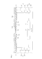
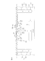
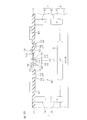
- FIG. 1 is a schematic plan view for explaining the configuration of the semiconductor device according to the first embodiment of the present invention.
- FIG. 2 is a schematic cross-sectional view taken along the line II-II of FIG.
- FIG. 3 is a schematic cross-sectional view showing an example of a simulation model relating to a comparative example.
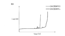
- FIG. 4 is a graph showing the simulation results for the comparative example.
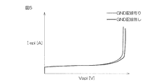
- FIG. 5 is a graph showing the simulation results for the present embodiment.
- FIG. 6A is a cross-sectional view showing an example of a manufacturing process of the semiconductor device shown in FIGS. 1 and 2, and is a cross-sectional view corresponding to the cut surface of FIG.
- FIG. 6B is a cross-sectional view showing the next step of FIG. 6A.
- FIG. 6C is a cross-sectional view showing the next step of FIG. 6B.
- FIG. 6D is a cross-sectional view showing the next step of FIG. 6C.
- FIG. 6E is a cross-sectional view showing the next step of FIG. 6D.
- FIG. 6F is a cross-sectional view showing the next step of FIG. 6E.
- FIG. 6G is a cross-sectional view showing the next step of FIG. 6F.
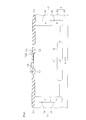
- FIG. 7 is a schematic plan view for explaining the configuration of the semiconductor device according to the second embodiment of the present invention.
- FIG. 10 is a schematic plan view for explaining the configuration of the semiconductor device according to the third embodiment of the present invention.
- FIG. 11 is a schematic cross-sectional view taken along the line Xl-Xl of FIG. 12A is a cross-sectional view showing an example of the manufacturing process of the semiconductor device shown in FIGS.
- FIG. 12B is a cross-sectional view showing the next step of FIG. 12A.
- FIG. 12C is a cross-sectional view showing the next step of FIG. 12B.
- FIG. 1 is a schematic plan view for explaining the configuration of the semiconductor device according to the first embodiment of the present invention.
- FIG. 2 is a schematic cross-sectional view taken along the line II-II of FIG. In FIG. 1, the interlayer insulating film 21 and the source wiring 26 shown in FIG. 2 are omitted. However, the drain wiring 25 shown in FIG. 2 is shown in FIG.
- the horizontal direction of the paper surface of FIG. 1 will be referred to as the horizontal direction
- the vertical direction of the paper surface of FIG. 1 will be referred to as the vertical direction.
- the semiconductor device 1 includes a substrate 3.
- the substrate 3 includes a p-type semiconductor substrate 4 and an n - type epitaxial layer 5 formed on the p-type semiconductor substrate 4.
- the p-type semiconductor substrate 4 is a silicon substrate.
- the p-type semiconductor substrate 4 is an example of the "p-type substrate” of the present invention
- the n - type epitaxial layer 5 is an example of the "n-type semiconductor layer" of the present invention.
- the film thickness of the n - type epitaxial layer 5 is, for example, about 3.0 ⁇ m to 10 ⁇ m.
- a p-type element separation region 7 for partitioning the element region 2 is formed on the surface layer portion of the substrate 3.
- the element region 2 has a rectangular shape that is long in the vertical direction in a plan view.
- a DMOS transistor 40 having an n- type epitaxial layer 5 as a drain is formed in the element region 2.
- the p-type element separation region film 7 is endless in a plan view.
- the p-type element separation region 7 has a rectangular ring shape in a plan view, but may have an endless shape such as an annular shape or an elliptical ring shape.
- the p-type element separation region 7 includes a lower separation region 8 connected to the p-type semiconductor substrate and an upper separation region 9 formed on the lower separation region 8.
- the substrate 3 is partitioned on the p-type semiconductor substrate 4 with an element region 2 composed of a part of the n-type epitaxial layer 5 surrounded by the p-type element separation region 7.
- the p-type element separation region 7 and the p-type semiconductor substrate 4 are grounded.
- n + type embedded layer 6 having a high value is selectively formed.
- the n + type embedded layer 6 is formed in a central region surrounded by a peripheral portion of the element region 2 in a plan view.
- the film thickness of the n + type embedded layer 6 is, for example, about 2.0 ⁇ m to 10.0 ⁇ m.
- an element region (not shown) in which an element different from the DMOS transistor 40 is formed in the element region 2 is partitioned in the outer peripheral region of the element region 2.
- An endless field insulating film 11 is formed on the surface of the p-type element separation region 7 in a plan view.
- the field insulating film 11 is formed in a square ring shape in a plan view so as to surround the region surrounded by the peripheral edge portion of the element region 2.
- the field insulating film 11 is wider than the p-type element separation region 7 and is formed so as to completely cover the p-type element separation region 7.
- the field insulating film 11 is, for example, a LOCOS film formed by selectively oxidizing the surface of the n-type epitaxial layer 5.
- the DMOS transistor 40 includes an n-type drain region 13 and a p-type well region 15 formed on the surface layer portion of the n-type epitaxial layer 5 at intervals from each other.
- the p-type well region 15 has a rectangular shape elongated in the vertical direction in a plan view, and is formed in the central portion in the horizontal direction of the element region 2.
- the n-type drain region 13 has a higher impurity concentration than that of the n-type epitaxial layer 5.
- the n-type drain region 13 is formed in an endless shape so as to surround the p-type well region 15 in a plan view.
- the n-type drain region 13 is formed in a square ring along the field insulating film 11 in a plan view.
- An n + type drain contact region 14 having a higher impurity concentration than the n-type drain region 13 is formed on the surface layer portion of the n-type drain region 13.
- n-type source region 16 having a higher impurity concentration than the n- type epitaxial layer 5 is formed on the surface layer of the p-type well region 15.
- An n + type source contact region 17 having a higher impurity concentration than the n-type source region 16 is formed on the surface layer portion of the n-type source region 16.
- the n-type source region 16 is formed, for example, at the same concentration and depth as the n-type drain region 13.
- the outer peripheral edge of the n + type source contact region 17 is arranged at a space inward from the outer peripheral edge of the p-type well region 15.
- the n + type source contact region 17 is formed, for example, at the same concentration and the same depth as the n + type drain contact region 14.
- a square annular field insulating film 12 in a plan view is formed in a portion between the n + type drain contact region 14 and the p-type well region 15.
- the field insulating film 12 is a LOCOS film formed in the same process as the above-mentioned field insulating film 11.
- the inner peripheral edge of the field insulating film 12 is indicated by reference numeral 12a.
- the inner peripheral edge 12a of the field insulating film 12 is arranged at an interval outward from the outer peripheral edge of the p-type well region 15, and the outer peripheral edge of the field insulating film 12 is placed on the inner peripheral edge of the n + type drain contact region 14. It is arranged.
- the n + type drain contact region 14 is formed in a region sandwiched between the outer peripheral edge of the field insulating film 12 and the inner peripheral edge of the field insulating film 11.
- n - the surface of the type epitaxial layer 5 n - gate insulating film 18 is formed so as to extend between the type epitaxial layer 5 and the p-type well region 15.
- the gate insulating film 18 is formed in a square ring shape so as to surround the n + type source contact region 17 in a plan view.
- the gate electrode 19 is formed on the gate insulating film 18.
- the gate electrode 19 is formed in a square ring shape so as to surround the n-type source region 16 in a plan view.
- the gate electrode 19 is formed so as to selectively cover a part of the gate insulating film 18 and a part of the field insulating film 12.
- the gate electrode 19 is made of polysilicon, for example.
- the gate insulating film 18 is, for example, a silicon oxide film formed by oxidizing the surface of the n-type epitaxial layer 5.
- the region where the gate electrode 19 faces the p-type well region 15 via the gate insulating film 18 is the channel region 20 of the DMOS transistor 40.
- the formation of channels in the channel region 20 is controlled by the gate electrode 19.
- the interlayer insulating film 21 is formed so as to cover the entire element region 2.
- the interlayer insulating film 21 is formed of, for example, an insulating film such as an oxide film or a nitride film.
- a drain contact plug 22, a source contact plug 23, and a gate contact plug 24 are embedded in the interlayer insulating film 21.
- the lower end of the drain contact plug 22 is electrically connected to the n + type drain contact region 14.
- the lower end of the source contact plug 23 is electrically connected to the n + type source contact region 17.
- the gate contact plug 24 is electrically connected to the gate electrode 19.
- a drain wiring 25, a source wiring 26, and a gate wiring are formed on the interlayer insulating film 21.
- the area of the drain wiring 25 is shown as a dot hatching area.
- the drain wiring 25 is electrically connected to the n + type drain contact region 14 via a plurality of drain contact plugs 22.
- the source wiring 26 is electrically connected to the n + type source contact region 17 via a plurality of source contact plugs 23.
- the gate wiring is electrically connected to the gate electrode 19 via a plurality of gate contact plugs 24.
- the source wiring 26 has a rectangular shape that is long in the vertical direction in a plan view and covers an intermediate length between both ends of the gate electrode 19.
- a plurality of locations at the center of the width of the source wiring 26 are electrically connected to the n + type source contact region 17 via a plurality of source contact plugs 23.
- the gate wiring is electrically connected to both ends of the gate electrode 19 via a plurality of gate contact plugs 24.
- the drain wiring 25 is formed in a square ring shape so as to surround the field insulating film 12 in a plan view.
- the inner peripheral edge of the drain wiring 25 is substantially directly above the inner peripheral edge of the n + type drain contact region 14.
- the outer peripheral edge of the drain wiring 25 is outside the outer peripheral edge of the n + type drain contact region 14.
- the drain wiring 25 includes a main wiring portion 25A arranged directly above the n + type drain contact region 14, and an extension portion 25B extending outward from the outer peripheral edge of the main wiring portion 25A.
- the extension portion 25B constitutes the "conductive wiring" of the present invention (hereinafter, may be referred to as "withstand voltage improving wiring").
- the extension portion (withstand voltage improving wiring) 25B is a square ring in a plan view, and extends from the outer peripheral edge of the n + type drain contact region 14 toward the p-type element separation region 7 outside the outer peripheral edge.
- the extension portion 25B in plan view, from the outer peripheral edge of the n + -type drain contact region 14, the inner peripheral edge of the p-type isolation region 7 the outer peripheral edge and its outer n + -type drain contact region 14 It extends almost to the center of the width between.
- the extension portion (withstand voltage improving wiring) 25B is a peripheral edge region of the element region 2, and is between the outer peripheral edge of the n + type drain contact region 14 and the inner peripheral edge of the p-type element separation region 7 outside the outer peripheral edge. It is arranged so as to cover a part of the element termination region 30.
- the extension portion 25B may extend outward from the outer peripheral edge of the n + type drain contact region 14 in a plan view. Therefore, the extension portion 25B in plan view, for example, from the outer peripheral edge of the n + -type drain contact region 14, the outer peripheral edge of the n + -type drain contact region 14 and the inner periphery of the p-type isolation region 7 of the outer It may extend to an arbitrary position between them, or may extend outward from the inner peripheral edge of the p-type element separation region 7.
- other wiring when running through the can due to the influence of the potential of the other wiring, n - -type epitaxial layer 5 and the p
- the isopotential distribution may be disturbed, and the withstand voltage may decrease. If the potential of the other wiring is the same as the potential (drain voltage) of the element region 2, the equipotential distribution is not disturbed, but if the potential of the other wiring is the ground potential, the isobaric distribution is disturbed.
- the drain wiring 25 is formed with an extension portion (withstand voltage improving wiring) 25B that covers at least a part of the element termination region 30.
- a wiring having the same potential as the element region 2 (withstand voltage improving wiring) can be obtained so as to be arranged on the element termination region 30. Therefore, even if the potential of the other wiring is the ground potential, the influence of the potential of the other wiring is obtained. Can be suppressed.
- the potential of the other wiring is the ground potential, the disturbance of the equipotential distribution can be suppressed, the decrease in the withstand voltage of the DMOS transistor 40 can be suppressed, or the withstand voltage can be improved.
- the semiconductor device 1 of FIGS. 1 and 2 is referred to as "the present embodiment", and the configuration in which the drain wiring 25 is not provided with the extension portion 25B in the semiconductor device 1 of FIGS. 1 and 2 is referred to as a "comparative example”. do. That is, in the comparative example, the drain wiring 25 is composed of only the main wiring portion 25A of the present embodiment.
- a first simulation model 101 in which a wiring 50 (hereinafter referred to as “GND wiring”) having a potential of ground potential is arranged on the element termination region 30 is used.
- the withstand voltage of the comparative example was calculated.
- the parts corresponding to FIG. 2 described above are designated by the same reference numerals as those in FIG.
- the withstand voltage of the comparative example was calculated using the second simulation model in which the GND wiring is not arranged on the element termination region 30.
- the reverse voltage applied to the parasitic diode existing between the n- type epitaxial layer 5 (n + type drain contact region 14) and the p-type element separation region 7 is defined as V epi [V]. .. Further, the reverse current flowing through the parasitic diode is defined as I epi [A]. The reverse current I epi when the reverse voltage V epi was gradually increased was calculated by simulation.
- the withstand voltage of the present embodiment was calculated using the third simulation model in which the GND wiring is arranged on the element termination region 30. Further, regarding the present embodiment, the withstand voltage of the present embodiment was calculated using the fourth simulation model in which the GND wiring is not arranged.
- FIG. 4 is a graph showing the simulation results for the comparative example.
- the broken line is a graph showing the simulation result when the GND wiring is present
- the solid line is the graph showing the simulation result when the GND wiring is not present.
- FIG. 5 is a graph showing the simulation results for this embodiment.
- the broken line is a graph showing the simulation result when the GND wiring is present
- the solid line is the graph showing the simulation result when the GND wiring is not present.
- the breakdown voltage is lower when the GND wiring is present than when the GND wiring is not present. Further, in the comparative example, the absolute value difference between the breakdown voltage when the GND wiring is present and the breakdown voltage when the GND wiring is not present is relatively large.
- the breakdown voltage when the GND wiring is present and the breakdown voltage when the GND wiring is not present are substantially equal to each other. Moreover, the breakdown voltage when the GND wiring in the present embodiment does not exist is higher than the breakdown voltage when the GND wiring does not exist in the comparative example.
- the withstand voltage when the other wiring of the ground potential exists is almost equal to the withstand voltage when the other wiring of the ground potential does not exist.
- the withstand voltage of the DMOS transistor does not decrease so much even if other wiring having a ground potential is present.
- the withstand voltage when other wiring of the ground potential is present is higher than that of the comparative example. Further, in the present embodiment, the withstand voltage when there is no other wiring of the ground potential is also higher than that of the comparative example.
- the GND wiring is present as compared with the comparative example.
- the absolute difference in breakdown voltage when it does not exist has become smaller.
- the outward protrusion amount of the extension portion (withstand voltage improving wiring) 25B When was about half of L (about 0.5 L), the withstand voltage became the largest.
- FIGS. 6A to 6G are cross-sectional views for explaining an example of the manufacturing process of the semiconductor device 1, and are cross-sectional views corresponding to the cut surface of FIG.
- a p-type semiconductor substrate 4 is prepared as shown in FIG. 6A.
- the n-type impurities and the p-type impurities are selectively injected onto the surface of the p-type semiconductor substrate 4.
- silicon is epitaxially grown on the p-type semiconductor substrate 4 while adding n-type impurities.
- FIG. 6B the substrate 3 including the p-type semiconductor substrate 4 and the n- type epitaxial layer 5 is formed.
- the n-type impurities and p-type impurities injected into the p-type semiconductor substrate 4 diffuse in the growth direction of the n-type epitaxial layer 5.
- an n + type embedded layer 6 straddling the boundary between the p-type semiconductor substrate 4 and the n - type epitaxial layer 5 and a p-type lower separation region 8 are formed.
- the p-type impurity include B (boron) and Al (aluminum)
- examples of the n-type impurity include P (phosphorus) and As (arsenic).
- an ion implantation mask (not shown) having an opening selectively in the region where the p-type upper separation region 9 should be formed is formed on the n-type epitaxial layer 5. Then, the p-type impurity is implanted into the n - type epitaxial layer 5 through the ion implantation mask. As a result, the p-type element separation region 7 having a two-layer structure of the lower separation region 8 and the upper separation region 9 is formed. After this, the ion implantation mask is removed.
- a hard mask 51 having an opening selectively in the region where the field insulating films 11 and 12 are to be formed is formed on the n - type epitaxial layer 5. Then, the surface of the n- type epitaxial layer 5 is subjected to thermal oxidation treatment via the hard mask 51 to form the field insulating films 11 and 12. After this, the hard mask 51 is removed.
- the surface of the n- type epitaxial layer 5 is subjected to thermal oxidation treatment to form the gate insulating film 18.
- the gate insulating film 18 is formed so as to be connected to the field insulating films 11 and 12.
- the polysilicon for the gate electrode 19 is deposited on the n- type epitaxial layer 5, and the polysilicon layer 52 is formed.
- a resist mask (not shown) having an opening selectively in the region where the gate electrode 19 should be formed is formed on the polysilicon layer 52. Then, an unnecessary portion of the polysilicon layer 52 is removed by etching via the resist mask. As a result, the gate electrode 19 is formed. After this, the resist mask is removed.
- a hard mask (not shown) having an opening selectively is formed on the n- type epitaxial layer 5. Then, an unnecessary portion of the gate insulating film 18 is etched through the hard mask. As a result, a predetermined gate insulating film 18 is formed. After this, the hard mask is removed. The step of selectively etching the gate insulating film 18 may be omitted.
- a p-type well region 15 is formed on the surface layer portion of the n-type epitaxial layer 5.
- an ion implantation mask (not shown) having an opening selectively in the region where the p-type well region 15 should be formed is formed.
- the p-type impurity is implanted into the n - type epitaxial layer 5 through the ion implantation mask.
- the p-type impurities are thermally diffused, for example, at a temperature of 900 ° C. to 1100 ° C.
- the ion implantation mask is removed.
- the p-type well region 15 is formed by selectively injecting p-type impurities into the n- type epitaxial layer 5 before the gate insulating film 18 and the gate electrode 19 are formed (FIG. 6C). You may.
- n - n-type source region 16 inwardly region (surface layer portion) of the p-type well region 15 and at the same time the n-type drain region 13 is formed in a surface portion of the type epitaxial layer 5 is formed.
- ion implantation having an opening selectively in each of the region where the n-type drain region 13 should be formed and the region where the n-type source region 16 should be formed.
- a mask (not shown) is formed.
- the n-type impurity is implanted into the n - type epitaxial layer 5 through the ion implantation mask.
- the n-type drain region 13 and the n-type source region 16 are formed.
- the ion implantation mask is removed.
- the n + type drain contact region 14 and the n + type source contact region 17 are selectively formed in each inner region (surface layer portion) of the n-type drain region 13 and the n-type source region 16.
- an opening is selectively opened in each of the areas where the n + type drain contact area 14 and the n + type source contact area 17 should be formed.
- An ion implantation mask (not shown) is formed.
- the n-type impurity is injected into the n-type drain region 13 and the n-type source region 16 through the ion implantation mask.
- the n + type drain contact region 14 and the n + type source contact region 17 are formed.
- the ion implantation mask is removed.
- an insulating material is deposited so as to cover the gate electrode 19, and an interlayer insulating film 21 is formed.
- the drain contact plug 22, the source contact plug 23, and the gate contact plug 24 are formed so as to penetrate the interlayer insulating film 21.
- the drain contact plug 22, the source contact plug 23, and the gate contact plug 24 are electrically connected to the n + type drain contact region 14, the n + type source contact region 17, and the gate electrode 19, respectively.
- the drain wiring 25, the source wiring 26, and the gate wiring (not shown) electrically connected to the drain contact plug 22, the source contact plug 23, and the gate contact plug 24 are placed on the interlayer insulating film 21. It is selectively formed.
- a wiring material layer is formed on the interlayer insulating film 21.
- the drain wiring 25, the source wiring 26, and the gate wiring are formed by selectively removing the wiring material layer by photolithography and etching.
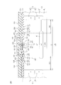
- FIG. 7 is a schematic plan view for explaining the configuration of the semiconductor device according to the second embodiment of the present invention.
- FIG. 8 is a schematic cross-sectional view taken along the line VIII-VIII of FIG. In FIG. 7, the interlayer insulating film 21, the drain wiring 25, and the source wiring 26 shown in FIG. 8 are omitted. However, the withstand voltage improving wiring 65 shown in FIG. 8 is shown in FIG. 7.
- FIG. 7 the parts corresponding to the respective parts of FIG. 1 described above are designated by the same reference numerals as those in FIG.
- FIG. 8 the portions corresponding to the respective parts of FIG. 2 described above are designated by the same reference numerals as those in FIG.
- the semiconductor device 1A according to the second embodiment has a different configuration of the withstand voltage improving wiring than the semiconductor device 1 according to the first embodiment described above.
- the withstand voltage improving wiring is configured by the extension portion 25B of the drain wiring 25.
- the withstand voltage improving wiring is provided independently of the drain wiring 25.
- the inner peripheral edge of the field insulating film 11 covering the surface of the p-type element separation region 7 is located at a position separated from the outer peripheral edge of the n + type drain contact region 14 by a certain distance in a plan view. positioned.
- N - -type epitaxial layer 5 In the region between the n-type drain region 13 and the field insulating film 11 in Heimen view, N - -type epitaxial layer 5, and at a n-type drain region 13 and spacing, N-type regions 61 are formed.
- the n-type region 61 is formed in a square ring along the field insulating film 11 so as to surround the n-type drain region 13 in a plan view.
- the impurity concentration of the n-type region 61 is substantially equal to the impurity concentration of the n-type drain region 13.
- An n + type contact region 62 for withstand voltage improving wiring having a higher impurity concentration than the n-type region 61 is formed on the surface layer portion of the n-type region 61.
- the impurity concentration of the n + type contact region 62 is substantially equal to the impurity concentration of the n + type drain contact region 14.
- a rectangular annular field insulating film 63 in a plan view is formed in a portion between the n + type contact region 62 and the n + type drain contact region 14.
- the field insulating film 63 is a LOCOS film formed in the same process as the above-mentioned field insulating films 11 and 12.
- a contact plug 64 for pressure resistance improving wiring is embedded in the interlayer insulating film 21, in addition to the drain contact plug 22, the source contact plug 23, and the gate contact plug 24, a contact plug 64 for pressure resistance improving wiring is embedded.
- the lower end of the contact plug 64 is electrically connected to the n + type contact region 62.
- the withstand voltage improving wiring 65 is formed on the interlayer insulating film 21.
- the region of the withstand voltage improving wiring 65 is shown as a dot hatching region.
- the drain wiring 25 is composed of only the main wiring portion 25A of the drain wiring 25 of the first embodiment.
- the withstand voltage improving wiring 65 is electrically connected to the n + type contact region 62 via a plurality of contact plugs 64.
- the withstand voltage improving wiring 65 is formed in a square ring shape so as to surround the field insulating film 63 in a plan view.
- the inner peripheral edge of the withstand voltage improving wiring 65 is substantially directly above the inner peripheral edge of the n + type contact region 62.
- the inner peripheral edge of the withstand voltage improving wiring 65 may be located closer to the outer peripheral edge of the n + type drain contact region 14 in a plan view.
- the outer peripheral edge of the withstand voltage improving wiring 65 is outside the outer peripheral edge of the n + type contact region 62.
- the outer peripheral edge of the withstand voltage improving wiring 65 is located between the outer peripheral edge of the n + type contact region 62 and the inner peripheral edge of the p-type element separation region 7 outside the outer peripheral edge of the n + type contact region 62 in a plan view.
- the withstand voltage improving wiring 65 is a peripheral edge region of the element region 2, and is an element termination region 30 between the outer peripheral edge of the n + type drain contact region 14 and the inner peripheral edge of the p-type element separation region 7 outside the n + type drain contact region 14. It is arranged so as to cover a part of (in this example, the middle part of the width).
- the withstand voltage improving wiring 65 that covers at least a part of the element termination region 30 is provided.
- the withstand voltage improving wiring 65 having the same potential as the element region 2 can be arranged on the element termination region 30, so that the influence of the potential of the other wiring is suppressed even when the potential of the other wiring is the ground potential. can.
- the equipotential distribution is disturbed when a reverse voltage is applied to the parasitic diode existing between the n-type epitaxial layer and the p-type element separation region 7. Can be suppressed.
- FIGS. 9A to 9E are cross-sectional views for explaining an example of the manufacturing process of the semiconductor device 1A, and are cross-sectional views corresponding to the cut surface of FIG.
- the p-type semiconductor substrate 4 is prepared in the same manner as in the manufacturing method of the semiconductor device 1 described above. Then, after the n-type impurities and the p-type impurities are selectively injected into the surface of the p-type semiconductor substrate 4, the p-type semiconductor substrate 4 is added while adding the n-type impurities, for example, in a heating environment of 1100 ° C. or higher. Impurity grow silicon on top. As a result, as shown in FIG. 6B, the substrate 3 including the p-type semiconductor substrate 4 and the n- type epitaxial layer 5 is formed. As a result, the n + type embedded layer 6 and the p-type lower separation region 8 straddling the boundary between the p-type semiconductor substrate 4 and the n -type epitaxial layer 5 are formed.
- an ion implantation mask (not shown) having an opening selectively in the region where the p-type upper separation region 9 should be formed is formed on the n-type epitaxial layer 5. Then, the p-type impurity is implanted into the n - type epitaxial layer 5 through the ion implantation mask. As a result, the p-type element separation region 7 having a two-layer structure of the lower separation region 8 and the upper separation region 9 is formed. After this, the ion implantation mask is removed.
- a hard mask 71 having an opening selectively in the region where the field insulating films 11, 12, and 63 should be formed is formed on the n - type epitaxial layer 5. Then, the surface of the n- type epitaxial layer 5 is subjected to thermal oxidation treatment via the hard mask 71 to form the field insulating films 11, 12, 63. After this, the hard mask 71 is removed.
- the surface of the n- type epitaxial layer 5 is subjected to thermal oxidation treatment to form the gate insulating film 18.
- the gate insulating film 18 is formed so as to be connected to the field insulating films 11, 63, 12.
- the polysilicon for the gate electrode 19 is deposited on the n- type epitaxial layer 5, and the polysilicon layer 72 is formed.
- a resist mask (not shown) having an opening selectively in the region where the gate electrode 19 should be formed is formed on the polysilicon layer 72. Then, an unnecessary portion of the polysilicon layer 72 is removed by etching via the resist mask. As a result, the gate electrode 19 is formed. After this, the resist mask is removed.
- a hard mask (not shown) having an opening selectively is formed on the n- type epitaxial layer 5. Then, an unnecessary portion of the gate insulating film 18 is etched through the hard mask. As a result, a predetermined gate insulating film 18 is formed. After this, the hard mask is removed. The step of selectively etching the gate insulating film 18 may be omitted.
- a p-type well region 15 is formed on the surface layer portion of the n-type epitaxial layer 5.
- an ion implantation mask (not shown) having an opening selectively in the region where the p-type well region 15 should be formed is formed.
- the p-type impurity is implanted into the n - type epitaxial layer 5 through the ion implantation mask.
- the p-type impurities are thermally diffused, for example, at a temperature of 900 ° C. to 1100 ° C.
- the ion implantation mask is removed.
- the p-type well region 15 is formed by selectively injecting p-type impurities into the n- type epitaxial layer 5 before the gate insulating film 18 and the gate electrode 19 are formed (FIG. 9A). You may.
- n - n-type source region 16 inwardly region (surface layer portion) of the p-type well region 15 and at the same time the n-type drain region 13 and the n-type region 61 is formed in a surface portion of the type epitaxial layer 5 is formed Will be done.
- the n-type drain region 13, the n-type region 61, and the n-type source region 16 are formed, for example, as follows.
- an ion implantation mask (not shown) having openings selectively in each of the region where the n-type drain region 13 should be formed, the region where the n-type region 61 should be formed, and the region where the n-type source region 16 should be formed (not shown). Is formed. Then, the n-type impurity is implanted into the n - type epitaxial layer 5 through the ion implantation mask. As a result, the n-type drain region 13, the n-type region 61, and the n-type source region 16 are formed. After this, the ion implantation mask is removed.
- the n + type drain contact region 14 is formed as follows, for example.
- an ion implantation mask (not shown) having openings selectively formed in each of the regions where the n + type drain contact region 14, the n + type contact region 62, and the n + type source contact region 17 should be formed is formed. .. Then, the n-type impurities are implanted into the n-type drain region 13, the n-type region 61, and the n-type source region 16 through the ion implantation mask. As a result, the n + type drain contact region 14, the n + type contact region 62, and the n + type source contact region 17 are formed. After this, the ion implantation mask is removed.
- an insulating material is deposited so as to cover the gate electrode 19, and an interlayer insulating film 21 is formed.
- the contact plug 64, the drain contact plug 22, the source contact plug 23, and the gate contact plug 24 are formed so as to penetrate the interlayer insulating film 21.
- the contact plug 64, the drain contact plug 22, the source contact plug 23, and the gate contact plug 24 are an n + type contact area 62, an n + type drain contact area 14, an n + type source contact area 17, and a gate electrode, respectively. Each of them is electrically connected to 19.
- the withstand voltage improving wiring 65, the drain wiring 25, the source wiring 26, and the gate wiring (not shown) that are electrically connected to the contact plug 64, the drain contact plug 22, the source contact plug 23, and the gate contact plug 24, respectively. ) Is selectively formed on the interlayer insulating film 21.
- the drain wiring 25, the source wiring 26, and the gate wiring for example, a wiring material layer is formed on the interlayer insulating film 21. Then, by selectively removing the wiring material layer by photolithography and etching, the withstand voltage improving wiring 65, the drain wiring 25, the source wiring 26, and the gate wiring are formed. Through the above steps, the semiconductor device 1A according to the second embodiment is manufactured.
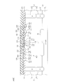
- FIG. 10 is a schematic plan view for explaining the configuration of the semiconductor device according to the third embodiment of the present invention.
- FIG. 11 is a schematic cross-sectional view taken along the line XI-XI of FIG.
- the interlayer insulating film 21, the drain wiring 25, and the source wiring 26 shown in FIG. 11 are omitted.
- the withstand voltage improving wiring 81 shown in FIG. 11 is shown in FIG.
- FIG. 10 the parts corresponding to the respective parts of FIG. 1 described above are designated by the same reference numerals as those in FIG.
- FIG. 11 the parts corresponding to the respective parts of FIG. 2 described above are designated by the same reference numerals as those in FIG.
- the semiconductor device 1B according to the third embodiment has a different configuration of the withstand voltage improving wiring than the semiconductor device 1 according to the first embodiment described above.
- the withstand voltage improving wiring is configured by the extension portion 25B of the drain wiring 25.
- the withstand voltage improving wiring is provided independently of the drain wiring 25.
- the drain wiring 25 has an extension portion 25B as in the first embodiment, and this extension portion 25B also functions as a withstand voltage improving wiring.
- the withstand voltage improving wiring 81 is formed on the field insulating film 11.
- the region of the withstand voltage improving wiring 81 is shown as a dot hatching region.
- the withstand voltage improving wiring 81 is formed in a square ring along the p-type element separation region 7 so as to surround the n + type drain contact region 14 in a plan view.
- the withstand voltage improving wiring 81 is made of polysilicon.
- the withstand voltage improving wiring 81 is covered with an interlayer insulating film 21.
- the withstand voltage improving wiring 81 is formed outward from the n + type drain contact region 14 in a plan view.
- the inner peripheral edge of the withstand voltage improving wiring 81 is located at a position separated from the n + type drain contact region 14 outward by a certain distance in a plan view.
- the inner peripheral edge of the withstand voltage improving wiring 81 may be directly above the outer peripheral edge of the n + type drain contact region 14.
- the outer peripheral edge of the withstand voltage improving wiring 81 is inside the inner peripheral edge of the p-type element separation region 7.
- the withstand voltage improving wiring 81 is a peripheral edge region of the element region 2, and is an element termination region 30 between the outer peripheral edge of the n + type drain contact region 14 and the inner peripheral edge of the p-type element separation region 7 outside the n + type drain contact region 14. It is arranged so as to cover a part of (in this example, the middle part of the width).
- the drain wiring 25 includes a main wiring portion 25A arranged directly above the n + type drain contact region 14, and an extension portion 25B extending outward from the outer peripheral edge of the main wiring portion 25A.
- the extension portion 25B has a superposed portion that overlaps the surface of the withstand voltage improving wiring 81 in a plan view.
- a plurality of contact plugs 82 for electrically connecting the superposed portion of the extension portion 25B and the withstand voltage improving wiring 81 are embedded in the interlayer insulating film 21.
- the withstand voltage improving wiring 81 is electrically connected to the drain wiring 25 via a plurality of contact plugs 82. Therefore, the withstand voltage improving wiring 81 is electrically connected to the n- type epitaxial layer 5 via the contact plug 82, the drain wiring 25, and the drain contact plug 22.
- the withstand voltage improving wiring 81 that covers at least a part of the element termination region 30 is provided.
- the withstand voltage improving wiring 81 having the same potential as the element region 2 can be arranged on the element termination region 30, so that the influence of the potential of the other wiring is suppressed even when the potential of the other wiring is the ground potential. can.
- the equipotential distribution is disturbed when a reverse voltage is applied to the parasitic diode existing between the n-type epitaxial layer and the p-type element separation region 7. Can be suppressed.
- FIGS. 12A to 12C are cross-sectional views for explaining an example of the manufacturing process of the semiconductor device 1B, and is a cross-sectional view corresponding to the cut surface of FIG.
- FIGS. 6A to 6D are applied as they are to the manufacturing method of the semiconductor device 1B.
- polysilicon is deposited on the n- type epitaxial layer 5 and the polysilicon layer 52 is formed by the step of FIG. 6D, as shown in FIG. 12A, the region where the gate electrode 19 should be formed and the withstand voltage improving wiring.
- a resist mask (not shown) having openings selectively in each region where 81 should be formed is formed on the polysilicon layer 52. Then, an unnecessary portion of the polysilicon layer 52 is removed by etching via the resist mask. As a result, the gate electrode 19 and the withstand voltage improving wiring 81 are formed at the same time. After this, the resist mask is removed.
- a hard mask (not shown) having an opening selectively is formed on the n- type epitaxial layer 5. Then, an unnecessary portion of the gate insulating film 18 is etched through the hard mask. As a result, a predetermined gate insulating film 18 is formed. After this, the hard mask is removed. The step of selectively etching the gate insulating film 18 may be omitted.
- a p-type well region 15 is formed on the surface layer portion of the n-type epitaxial layer 5.
- an ion implantation mask (not shown) having an opening selectively in the region where the p-type well region 15 should be formed is formed.
- the p-type impurity is implanted into the n - type epitaxial layer 5 through the ion implantation mask.
- the p-type impurities are thermally diffused, for example, at a temperature of 900 ° C. to 1100 ° C.
- the ion implantation mask is removed.
- the p-type well region 15 is formed by selectively injecting p-type impurities into the n- type epitaxial layer 5 before the gate insulating film 18 and the gate electrode 19 are formed (FIG. 6C). You may.
- n - n-type source region 16 inwardly region (surface layer portion) of the p-type well region 15 and at the same time the n-type drain region 13 is formed in a surface portion of the type epitaxial layer 5 is formed.
- ion implantation having an opening selectively in each of the region where the n-type drain region 13 should be formed and the region where the n-type source region 16 should be formed.
- a mask (not shown) is formed.
- the n-type impurity is implanted into the n - type epitaxial layer 5 through the ion implantation mask.
- the n-type drain region 13 and the n-type source region 16 are formed.
- the ion implantation mask is removed.
- the n + type drain contact region 14 and the n + type source contact region 17 are selectively formed in each inner region (surface layer portion) of the n-type drain region 13 and the n-type source region 16.
- an opening is selectively opened in each of the areas where the n + type drain contact area 14 and the n + type source contact area 17 should be formed.
- An ion implantation mask (not shown) is formed.
- the n-type impurity is injected into the n-type drain region 13 and the n-type source region 16 through the ion implantation mask.
- the n + type drain contact region 14 and the n + type source contact region 17 are formed.
- the ion implantation mask is removed.
- an insulating material is deposited so as to cover the gate electrode 19 and the withstand voltage improving wiring 81 to form the interlayer insulating film 21.
- the drain contact plug 22, the source contact plug 23, the gate contact plug 24, and the contact plug 82 are formed so as to penetrate the interlayer insulating film 21.
- the drain contact plug 22, the source contact plug 23, the gate contact plug 24, and the contact plug 82 are connected to the n + type drain contact area 14, the n + type source contact area 17, the gate electrode 19, and the withstand voltage improving wiring 81, respectively. Each is electrically connected.
- drain wiring 25, the source wiring 26, and the gate wiring are selectively formed on the interlayer insulating film 21.
- the drain wiring 25 is electrically connected to the drain contact plug 22 and the withstand voltage improving wiring contact plug 82.
- the source wiring 26 and the gate wiring are electrically connected to the source contact plug 23 and the gate contact plug 24, respectively.
Landscapes
- Insulated Gate Type Field-Effect Transistor (AREA)
- Metal-Oxide And Bipolar Metal-Oxide Semiconductor Integrated Circuits (AREA)
Priority Applications (4)
| Application Number | Priority Date | Filing Date | Title |
|---|---|---|---|
| US17/797,295 US11984502B2 (en) | 2020-03-13 | 2021-03-03 | Semiconductor device with suppression of decrease of withstand voltage, and method for manufacturing the semiconductor device |
| CN202180020822.4A CN115280514B (zh) | 2020-03-13 | 2021-03-03 | 半导体器件及其制造方法 |
| JP2022505960A JP7728243B2 (ja) | 2020-03-13 | 2021-03-03 | 半導体装置およびその製造方法 |
| DE112021001612.1T DE112021001612T5 (de) | 2020-03-13 | 2021-03-03 | Halbleiterbauteil und Verfahren zum Herstellen desselben |
Applications Claiming Priority (2)
| Application Number | Priority Date | Filing Date | Title |
|---|---|---|---|
| JP2020044368 | 2020-03-13 | ||
| JP2020-044368 | 2020-03-13 |
Publications (1)
| Publication Number | Publication Date |
|---|---|
| WO2021182211A1 true WO2021182211A1 (ja) | 2021-09-16 |
Family
ID=77671633
Family Applications (1)
| Application Number | Title | Priority Date | Filing Date |
|---|---|---|---|
| PCT/JP2021/008083 Ceased WO2021182211A1 (ja) | 2020-03-13 | 2021-03-03 | 半導体装置およびその製造方法 |
Country Status (5)
| Country | Link |
|---|---|
| US (1) | US11984502B2 (https=) |
| JP (1) | JP7728243B2 (https=) |
| CN (1) | CN115280514B (https=) |
| DE (1) | DE112021001612T5 (https=) |
| WO (1) | WO2021182211A1 (https=) |
Families Citing this family (1)
| Publication number | Priority date | Publication date | Assignee | Title |
|---|---|---|---|---|
| KR20260019292A (ko) * | 2024-08-01 | 2026-02-10 | 삼성전자주식회사 | 전력 반도체 소자 |
Citations (6)
| Publication number | Priority date | Publication date | Assignee | Title |
|---|---|---|---|---|
| JPS59193065A (ja) * | 1983-04-15 | 1984-11-01 | Matsushita Electric Works Ltd | トランジスタ装置 |
| JPH04127573A (ja) * | 1990-09-19 | 1992-04-28 | Fuji Electric Co Ltd | 2重拡散型misfetを備えた半導体装置及びその製造方法 |
| JP2002314066A (ja) * | 2001-04-13 | 2002-10-25 | Sanyo Electric Co Ltd | Mos半導体装置およびその製造方法 |
| JP2007180244A (ja) * | 2005-12-27 | 2007-07-12 | Sanyo Electric Co Ltd | 半導体装置及びその製造方法 |
| WO2012127960A1 (ja) * | 2011-03-18 | 2012-09-27 | ルネサスエレクトロニクス株式会社 | 半導体装置およびその製造方法 |
| JP2018011089A (ja) * | 2017-10-23 | 2018-01-18 | ローム株式会社 | 半導体装置 |
Family Cites Families (10)
| Publication number | Priority date | Publication date | Assignee | Title |
|---|---|---|---|---|
| JPH01138753A (ja) * | 1987-11-26 | 1989-05-31 | Fuji Electric Co Ltd | 半導体装置の内部漏洩電流防止構造 |
| JP4797225B2 (ja) * | 1999-05-27 | 2011-10-19 | 富士電機株式会社 | 半導体装置 |
| US6911694B2 (en) * | 2001-06-27 | 2005-06-28 | Ricoh Company, Ltd. | Semiconductor device and method for fabricating such device |
| JP4420196B2 (ja) * | 2003-12-12 | 2010-02-24 | 三菱電機株式会社 | 誘電体分離型半導体装置およびその製造方法 |
| JP4906281B2 (ja) * | 2005-03-30 | 2012-03-28 | オンセミコンダクター・トレーディング・リミテッド | 半導体装置 |
| CN100474588C (zh) * | 2005-03-30 | 2009-04-01 | 三洋电机株式会社 | 半导体装置 |
| JP5431637B2 (ja) * | 2006-09-29 | 2014-03-05 | セミコンダクター・コンポーネンツ・インダストリーズ・リミテッド・ライアビリティ・カンパニー | 半導体装置 |
| JP2008218446A (ja) * | 2007-02-28 | 2008-09-18 | Oki Electric Ind Co Ltd | Mosトランジスタとその製造方法 |
| JP5700649B2 (ja) | 2011-01-24 | 2015-04-15 | 旭化成エレクトロニクス株式会社 | 半導体装置の製造方法 |
| JP6509665B2 (ja) * | 2015-07-23 | 2019-05-08 | ルネサスエレクトロニクス株式会社 | 半導体装置 |
-
2021
- 2021-03-03 CN CN202180020822.4A patent/CN115280514B/zh active Active
- 2021-03-03 WO PCT/JP2021/008083 patent/WO2021182211A1/ja not_active Ceased
- 2021-03-03 US US17/797,295 patent/US11984502B2/en active Active
- 2021-03-03 JP JP2022505960A patent/JP7728243B2/ja active Active
- 2021-03-03 DE DE112021001612.1T patent/DE112021001612T5/de active Pending
Patent Citations (6)
| Publication number | Priority date | Publication date | Assignee | Title |
|---|---|---|---|---|
| JPS59193065A (ja) * | 1983-04-15 | 1984-11-01 | Matsushita Electric Works Ltd | トランジスタ装置 |
| JPH04127573A (ja) * | 1990-09-19 | 1992-04-28 | Fuji Electric Co Ltd | 2重拡散型misfetを備えた半導体装置及びその製造方法 |
| JP2002314066A (ja) * | 2001-04-13 | 2002-10-25 | Sanyo Electric Co Ltd | Mos半導体装置およびその製造方法 |
| JP2007180244A (ja) * | 2005-12-27 | 2007-07-12 | Sanyo Electric Co Ltd | 半導体装置及びその製造方法 |
| WO2012127960A1 (ja) * | 2011-03-18 | 2012-09-27 | ルネサスエレクトロニクス株式会社 | 半導体装置およびその製造方法 |
| JP2018011089A (ja) * | 2017-10-23 | 2018-01-18 | ローム株式会社 | 半導体装置 |
Also Published As
| Publication number | Publication date |
|---|---|
| CN115280514A (zh) | 2022-11-01 |
| DE112021001612T5 (de) | 2022-12-29 |
| CN115280514B (zh) | 2025-12-09 |
| JPWO2021182211A1 (https=) | 2021-09-16 |
| JP7728243B2 (ja) | 2025-08-22 |
| US20230045793A1 (en) | 2023-02-16 |
| US11984502B2 (en) | 2024-05-14 |
Similar Documents
| Publication | Publication Date | Title |
|---|---|---|
| US5525821A (en) | PN junction trench isolation type semiconductor device | |
| KR100957584B1 (ko) | 트렌치 mosfet 디바이스 및 이 디바이스를 형성하는 방법 | |
| US8384152B2 (en) | Semiconductor device having trench gate VDMOSFET and method of manufacturing the same | |
| JP3850146B2 (ja) | 分離構造とその分離構造を備える半導体装置 | |
| CN101409285B (zh) | 半导体装置及其制造方法 | |
| US20130341718A1 (en) | Power semiconductor device | |
| US8889518B2 (en) | LDMOS transistor with asymmetric spacer as gate | |
| US8017494B2 (en) | Termination trench structure for mosgated device and process for its manufacture | |
| JP5426112B2 (ja) | 半導体装置およびその製造方法 | |
| US9929259B2 (en) | Semiconductor device and manufacturing method for semiconductor device | |
| US20160260712A1 (en) | Semiconductor device and manufacturing method thereof | |
| CN101964343A (zh) | 半导体装置 | |
| JP7007971B2 (ja) | 半導体装置 | |
| JP6234715B2 (ja) | 半導体装置 | |
| WO2021182211A1 (ja) | 半導体装置およびその製造方法 | |
| JP2006526287A (ja) | 半導体装置のための終端構造及びこの構造の製造方法 | |
| US10038088B2 (en) | Power MOSFET having improved manufacturability, low on-resistance and high breakdown voltage | |
| JP6533266B2 (ja) | 半導体装置 | |
| JP2009043795A (ja) | 半導体装置 | |
| JP2006073626A (ja) | 半導体装置およびその製造方法 | |
| JP7737977B2 (ja) | 半導体装置およびその製造方法 | |
| US20230378272A1 (en) | Semiconductor device and method of manufacturing the same | |
| CN118039697B (zh) | 一种宽禁带半导体沟槽mosfet器件结构及其制作方法 | |
| JP4425295B2 (ja) | 半導体装置 | |
| CN100521244C (zh) | 结型场效应晶体管的制造方法 |
Legal Events
| Date | Code | Title | Description |
|---|---|---|---|
| 121 | Ep: the epo has been informed by wipo that ep was designated in this application |
Ref document number: 21768560 Country of ref document: EP Kind code of ref document: A1 |
|
| ENP | Entry into the national phase |
Ref document number: 2022505960 Country of ref document: JP Kind code of ref document: A |
|
| 122 | Ep: pct application non-entry in european phase |
Ref document number: 21768560 Country of ref document: EP Kind code of ref document: A1 |