WO2021182211A1 - Semiconductor device and method for manufacturing same - Google Patents
Semiconductor device and method for manufacturing same Download PDFInfo
- Publication number
- WO2021182211A1 WO2021182211A1 PCT/JP2021/008083 JP2021008083W WO2021182211A1 WO 2021182211 A1 WO2021182211 A1 WO 2021182211A1 JP 2021008083 W JP2021008083 W JP 2021008083W WO 2021182211 A1 WO2021182211 A1 WO 2021182211A1
- Authority
- WO
- WIPO (PCT)
- Prior art keywords
- type
- region
- wiring
- drain
- semiconductor device
- Prior art date
Links
- 239000004065 semiconductor Substances 0.000 title claims abstract description 104
- 238000004519 manufacturing process Methods 0.000 title description 15
- 238000000034 method Methods 0.000 title description 4
- 230000002093 peripheral effect Effects 0.000 claims abstract description 66
- 239000000758 substrate Substances 0.000 claims abstract description 46
- 239000010410 layer Substances 0.000 claims description 107
- 238000000926 separation method Methods 0.000 claims description 51
- 239000012535 impurity Substances 0.000 claims description 43
- 239000002344 surface layer Substances 0.000 claims description 31
- 229910021420 polycrystalline silicon Inorganic materials 0.000 claims description 17
- 229920005591 polysilicon Polymers 0.000 claims description 17
- 238000005192 partition Methods 0.000 claims description 2
- 238000006116 polymerization reaction Methods 0.000 claims 2
- 238000005468 ion implantation Methods 0.000 description 33
- 239000011229 interlayer Substances 0.000 description 23
- 230000000052 comparative effect Effects 0.000 description 15
- 238000004088 simulation Methods 0.000 description 15
- 230000015556 catabolic process Effects 0.000 description 8
- 238000005530 etching Methods 0.000 description 8
- 238000009826 distribution Methods 0.000 description 7
- 230000003071 parasitic effect Effects 0.000 description 6
- XUIMIQQOPSSXEZ-UHFFFAOYSA-N Silicon Chemical compound [Si] XUIMIQQOPSSXEZ-UHFFFAOYSA-N 0.000 description 4
- 239000000463 material Substances 0.000 description 4
- 230000003647 oxidation Effects 0.000 description 4
- 238000007254 oxidation reaction Methods 0.000 description 4
- 229910052710 silicon Inorganic materials 0.000 description 4
- 239000010703 silicon Substances 0.000 description 4
- 230000012447 hatching Effects 0.000 description 3
- 239000011810 insulating material Substances 0.000 description 3
- 238000010438 heat treatment Methods 0.000 description 2
- 238000002955 isolation Methods 0.000 description 2
- 230000001590 oxidative effect Effects 0.000 description 2
- 238000000206 photolithography Methods 0.000 description 2
- ZOXJGFHDIHLPTG-UHFFFAOYSA-N Boron Chemical compound [B] ZOXJGFHDIHLPTG-UHFFFAOYSA-N 0.000 description 1
- OAICVXFJPJFONN-UHFFFAOYSA-N Phosphorus Chemical compound [P] OAICVXFJPJFONN-UHFFFAOYSA-N 0.000 description 1
- VYPSYNLAJGMNEJ-UHFFFAOYSA-N Silicium dioxide Chemical compound O=[Si]=O VYPSYNLAJGMNEJ-UHFFFAOYSA-N 0.000 description 1
- 229910052782 aluminium Inorganic materials 0.000 description 1
- XAGFODPZIPBFFR-UHFFFAOYSA-N aluminium Chemical compound [Al] XAGFODPZIPBFFR-UHFFFAOYSA-N 0.000 description 1
- 229910052785 arsenic Inorganic materials 0.000 description 1
- RQNWIZPPADIBDY-UHFFFAOYSA-N arsenic atom Chemical compound [As] RQNWIZPPADIBDY-UHFFFAOYSA-N 0.000 description 1
- 230000015572 biosynthetic process Effects 0.000 description 1
- 229910052796 boron Inorganic materials 0.000 description 1
- 230000000694 effects Effects 0.000 description 1
- 238000009413 insulation Methods 0.000 description 1
- 229910044991 metal oxide Inorganic materials 0.000 description 1
- 150000004706 metal oxides Chemical class 0.000 description 1
- 150000004767 nitrides Chemical class 0.000 description 1
- 229910052698 phosphorus Inorganic materials 0.000 description 1
- 239000011574 phosphorus Substances 0.000 description 1
- 229910052814 silicon oxide Inorganic materials 0.000 description 1
- 238000000638 solvent extraction Methods 0.000 description 1
Images


Classifications
-
- H—ELECTRICITY
- H01—ELECTRIC ELEMENTS
- H01L—SEMICONDUCTOR DEVICES NOT COVERED BY CLASS H10
- H01L29/00—Semiconductor devices adapted for rectifying, amplifying, oscillating or switching, or capacitors or resistors with at least one potential-jump barrier or surface barrier, e.g. PN junction depletion layer or carrier concentration layer; Details of semiconductor bodies or of electrodes thereof ; Multistep manufacturing processes therefor
- H01L29/66—Types of semiconductor device ; Multistep manufacturing processes therefor
- H01L29/68—Types of semiconductor device ; Multistep manufacturing processes therefor controllable by only the electric current supplied, or only the electric potential applied, to an electrode which does not carry the current to be rectified, amplified or switched
- H01L29/76—Unipolar devices, e.g. field effect transistors
- H01L29/772—Field effect transistors
- H01L29/78—Field effect transistors with field effect produced by an insulated gate
- H01L29/7801—DMOS transistors, i.e. MISFETs with a channel accommodating body or base region adjoining a drain drift region
- H01L29/7816—Lateral DMOS transistors, i.e. LDMOS transistors
- H01L29/7817—Lateral DMOS transistors, i.e. LDMOS transistors structurally associated with at least one other device
- H01L29/7818—Lateral DMOS transistors, i.e. LDMOS transistors structurally associated with at least one other device the other device being a pn-junction diode
-
- H—ELECTRICITY
- H01—ELECTRIC ELEMENTS
- H01L—SEMICONDUCTOR DEVICES NOT COVERED BY CLASS H10
- H01L29/00—Semiconductor devices adapted for rectifying, amplifying, oscillating or switching, or capacitors or resistors with at least one potential-jump barrier or surface barrier, e.g. PN junction depletion layer or carrier concentration layer; Details of semiconductor bodies or of electrodes thereof ; Multistep manufacturing processes therefor
- H01L29/66—Types of semiconductor device ; Multistep manufacturing processes therefor
- H01L29/66007—Multistep manufacturing processes
- H01L29/66075—Multistep manufacturing processes of devices having semiconductor bodies comprising group 14 or group 13/15 materials
- H01L29/66227—Multistep manufacturing processes of devices having semiconductor bodies comprising group 14 or group 13/15 materials the devices being controllable only by the electric current supplied or the electric potential applied, to an electrode which does not carry the current to be rectified, amplified or switched, e.g. three-terminal devices
- H01L29/66409—Unipolar field-effect transistors
- H01L29/66477—Unipolar field-effect transistors with an insulated gate, i.e. MISFET
- H01L29/66674—DMOS transistors, i.e. MISFETs with a channel accommodating body or base region adjoining a drain drift region
- H01L29/66681—Lateral DMOS transistors, i.e. LDMOS transistors
-
- H—ELECTRICITY
- H01—ELECTRIC ELEMENTS
- H01L—SEMICONDUCTOR DEVICES NOT COVERED BY CLASS H10
- H01L23/00—Details of semiconductor or other solid state devices
- H01L23/52—Arrangements for conducting electric current within the device in operation from one component to another, i.e. interconnections, e.g. wires, lead frames
- H01L23/522—Arrangements for conducting electric current within the device in operation from one component to another, i.e. interconnections, e.g. wires, lead frames including external interconnections consisting of a multilayer structure of conductive and insulating layers inseparably formed on the semiconductor body
- H01L23/5222—Capacitive arrangements or effects of, or between wiring layers
-
- H—ELECTRICITY
- H01—ELECTRIC ELEMENTS
- H01L—SEMICONDUCTOR DEVICES NOT COVERED BY CLASS H10
- H01L29/00—Semiconductor devices adapted for rectifying, amplifying, oscillating or switching, or capacitors or resistors with at least one potential-jump barrier or surface barrier, e.g. PN junction depletion layer or carrier concentration layer; Details of semiconductor bodies or of electrodes thereof ; Multistep manufacturing processes therefor
- H01L29/02—Semiconductor bodies ; Multistep manufacturing processes therefor
- H01L29/06—Semiconductor bodies ; Multistep manufacturing processes therefor characterised by their shape; characterised by the shapes, relative sizes, or dispositions of the semiconductor regions ; characterised by the concentration or distribution of impurities within semiconductor regions
- H01L29/0603—Semiconductor bodies ; Multistep manufacturing processes therefor characterised by their shape; characterised by the shapes, relative sizes, or dispositions of the semiconductor regions ; characterised by the concentration or distribution of impurities within semiconductor regions characterised by particular constructional design considerations, e.g. for preventing surface leakage, for controlling electric field concentration or for internal isolations regions
- H01L29/0607—Semiconductor bodies ; Multistep manufacturing processes therefor characterised by their shape; characterised by the shapes, relative sizes, or dispositions of the semiconductor regions ; characterised by the concentration or distribution of impurities within semiconductor regions characterised by particular constructional design considerations, e.g. for preventing surface leakage, for controlling electric field concentration or for internal isolations regions for preventing surface leakage or controlling electric field concentration
- H01L29/0611—Semiconductor bodies ; Multistep manufacturing processes therefor characterised by their shape; characterised by the shapes, relative sizes, or dispositions of the semiconductor regions ; characterised by the concentration or distribution of impurities within semiconductor regions characterised by particular constructional design considerations, e.g. for preventing surface leakage, for controlling electric field concentration or for internal isolations regions for preventing surface leakage or controlling electric field concentration for increasing or controlling the breakdown voltage of reverse biased devices
- H01L29/0615—Semiconductor bodies ; Multistep manufacturing processes therefor characterised by their shape; characterised by the shapes, relative sizes, or dispositions of the semiconductor regions ; characterised by the concentration or distribution of impurities within semiconductor regions characterised by particular constructional design considerations, e.g. for preventing surface leakage, for controlling electric field concentration or for internal isolations regions for preventing surface leakage or controlling electric field concentration for increasing or controlling the breakdown voltage of reverse biased devices by the doping profile or the shape or the arrangement of the PN junction, or with supplementary regions, e.g. junction termination extension [JTE]
-
- H—ELECTRICITY
- H01—ELECTRIC ELEMENTS
- H01L—SEMICONDUCTOR DEVICES NOT COVERED BY CLASS H10
- H01L29/00—Semiconductor devices adapted for rectifying, amplifying, oscillating or switching, or capacitors or resistors with at least one potential-jump barrier or surface barrier, e.g. PN junction depletion layer or carrier concentration layer; Details of semiconductor bodies or of electrodes thereof ; Multistep manufacturing processes therefor
- H01L29/40—Electrodes ; Multistep manufacturing processes therefor
- H01L29/402—Field plates
- H01L29/404—Multiple field plate structures
-
- H—ELECTRICITY
- H01—ELECTRIC ELEMENTS
- H01L—SEMICONDUCTOR DEVICES NOT COVERED BY CLASS H10
- H01L29/00—Semiconductor devices adapted for rectifying, amplifying, oscillating or switching, or capacitors or resistors with at least one potential-jump barrier or surface barrier, e.g. PN junction depletion layer or carrier concentration layer; Details of semiconductor bodies or of electrodes thereof ; Multistep manufacturing processes therefor
- H01L29/66—Types of semiconductor device ; Multistep manufacturing processes therefor
- H01L29/68—Types of semiconductor device ; Multistep manufacturing processes therefor controllable by only the electric current supplied, or only the electric potential applied, to an electrode which does not carry the current to be rectified, amplified or switched
- H01L29/76—Unipolar devices, e.g. field effect transistors
- H01L29/772—Field effect transistors
- H01L29/78—Field effect transistors with field effect produced by an insulated gate
- H01L29/7801—DMOS transistors, i.e. MISFETs with a channel accommodating body or base region adjoining a drain drift region
- H01L29/7816—Lateral DMOS transistors, i.e. LDMOS transistors
- H01L29/7823—Lateral DMOS transistors, i.e. LDMOS transistors with an edge termination structure
-
- H—ELECTRICITY
- H01—ELECTRIC ELEMENTS
- H01L—SEMICONDUCTOR DEVICES NOT COVERED BY CLASS H10
- H01L21/00—Processes or apparatus adapted for the manufacture or treatment of semiconductor or solid state devices or of parts thereof
- H01L21/70—Manufacture or treatment of devices consisting of a plurality of solid state components formed in or on a common substrate or of parts thereof; Manufacture of integrated circuit devices or of parts thereof
- H01L21/71—Manufacture of specific parts of devices defined in group H01L21/70
- H01L21/76—Making of isolation regions between components
- H01L21/761—PN junctions
-
- H—ELECTRICITY
- H01—ELECTRIC ELEMENTS
- H01L—SEMICONDUCTOR DEVICES NOT COVERED BY CLASS H10
- H01L29/00—Semiconductor devices adapted for rectifying, amplifying, oscillating or switching, or capacitors or resistors with at least one potential-jump barrier or surface barrier, e.g. PN junction depletion layer or carrier concentration layer; Details of semiconductor bodies or of electrodes thereof ; Multistep manufacturing processes therefor
- H01L29/02—Semiconductor bodies ; Multistep manufacturing processes therefor
- H01L29/06—Semiconductor bodies ; Multistep manufacturing processes therefor characterised by their shape; characterised by the shapes, relative sizes, or dispositions of the semiconductor regions ; characterised by the concentration or distribution of impurities within semiconductor regions
- H01L29/0684—Semiconductor bodies ; Multistep manufacturing processes therefor characterised by their shape; characterised by the shapes, relative sizes, or dispositions of the semiconductor regions ; characterised by the concentration or distribution of impurities within semiconductor regions characterised by the shape, relative sizes or dispositions of the semiconductor regions or junctions between the regions
- H01L29/0692—Surface layout
-
- H—ELECTRICITY
- H01—ELECTRIC ELEMENTS
- H01L—SEMICONDUCTOR DEVICES NOT COVERED BY CLASS H10
- H01L29/00—Semiconductor devices adapted for rectifying, amplifying, oscillating or switching, or capacitors or resistors with at least one potential-jump barrier or surface barrier, e.g. PN junction depletion layer or carrier concentration layer; Details of semiconductor bodies or of electrodes thereof ; Multistep manufacturing processes therefor
- H01L29/02—Semiconductor bodies ; Multistep manufacturing processes therefor
- H01L29/06—Semiconductor bodies ; Multistep manufacturing processes therefor characterised by their shape; characterised by the shapes, relative sizes, or dispositions of the semiconductor regions ; characterised by the concentration or distribution of impurities within semiconductor regions
- H01L29/08—Semiconductor bodies ; Multistep manufacturing processes therefor characterised by their shape; characterised by the shapes, relative sizes, or dispositions of the semiconductor regions ; characterised by the concentration or distribution of impurities within semiconductor regions with semiconductor regions connected to an electrode carrying current to be rectified, amplified or switched and such electrode being part of a semiconductor device which comprises three or more electrodes
- H01L29/0843—Source or drain regions of field-effect devices
- H01L29/0847—Source or drain regions of field-effect devices of field-effect transistors with insulated gate
- H01L29/0852—Source or drain regions of field-effect devices of field-effect transistors with insulated gate of DMOS transistors
- H01L29/0856—Source regions
- H01L29/086—Impurity concentration or distribution
-
- H—ELECTRICITY
- H01—ELECTRIC ELEMENTS
- H01L—SEMICONDUCTOR DEVICES NOT COVERED BY CLASS H10
- H01L29/00—Semiconductor devices adapted for rectifying, amplifying, oscillating or switching, or capacitors or resistors with at least one potential-jump barrier or surface barrier, e.g. PN junction depletion layer or carrier concentration layer; Details of semiconductor bodies or of electrodes thereof ; Multistep manufacturing processes therefor
- H01L29/02—Semiconductor bodies ; Multistep manufacturing processes therefor
- H01L29/06—Semiconductor bodies ; Multistep manufacturing processes therefor characterised by their shape; characterised by the shapes, relative sizes, or dispositions of the semiconductor regions ; characterised by the concentration or distribution of impurities within semiconductor regions
- H01L29/08—Semiconductor bodies ; Multistep manufacturing processes therefor characterised by their shape; characterised by the shapes, relative sizes, or dispositions of the semiconductor regions ; characterised by the concentration or distribution of impurities within semiconductor regions with semiconductor regions connected to an electrode carrying current to be rectified, amplified or switched and such electrode being part of a semiconductor device which comprises three or more electrodes
- H01L29/0843—Source or drain regions of field-effect devices
- H01L29/0847—Source or drain regions of field-effect devices of field-effect transistors with insulated gate
- H01L29/0852—Source or drain regions of field-effect devices of field-effect transistors with insulated gate of DMOS transistors
- H01L29/0873—Drain regions
- H01L29/0878—Impurity concentration or distribution
-
- H—ELECTRICITY
- H01—ELECTRIC ELEMENTS
- H01L—SEMICONDUCTOR DEVICES NOT COVERED BY CLASS H10
- H01L29/00—Semiconductor devices adapted for rectifying, amplifying, oscillating or switching, or capacitors or resistors with at least one potential-jump barrier or surface barrier, e.g. PN junction depletion layer or carrier concentration layer; Details of semiconductor bodies or of electrodes thereof ; Multistep manufacturing processes therefor
- H01L29/40—Electrodes ; Multistep manufacturing processes therefor
- H01L29/41—Electrodes ; Multistep manufacturing processes therefor characterised by their shape, relative sizes or dispositions
- H01L29/423—Electrodes ; Multistep manufacturing processes therefor characterised by their shape, relative sizes or dispositions not carrying the current to be rectified, amplified or switched
- H01L29/42312—Gate electrodes for field effect devices
- H01L29/42316—Gate electrodes for field effect devices for field-effect transistors
- H01L29/4232—Gate electrodes for field effect devices for field-effect transistors with insulated gate
- H01L29/42364—Gate electrodes for field effect devices for field-effect transistors with insulated gate characterised by the insulating layer, e.g. thickness or uniformity
- H01L29/42368—Gate electrodes for field effect devices for field-effect transistors with insulated gate characterised by the insulating layer, e.g. thickness or uniformity the thickness being non-uniform
Definitions
- the present invention relates to a semiconductor device including a transistor such as a DMOS (Diffused Metal Oxide Semiconductor) transistor and a method for manufacturing the same.
- a transistor such as a DMOS (Diffused Metal Oxide Semiconductor) transistor and a method for manufacturing the same.
- Patent Document 1 discloses a semiconductor device including a p-type element separation region (p-type well) for separating the element region and a DMOS transistor formed in the element region.
- the semiconductor device includes a source region and a drain region selectively formed on the surface of an n-type epitaxial layer (n-type well) of a p-type substrate, and a gate electrode formed on the silicon substrate via a gate oxide film.
- a DMOS transistor may be mixedly mounted with another element.
- other elements a plurality of wirings electrically connected to other elements (hereinafter, referred to as “other elements”) other than the DMOS transistor (hereinafter referred to as “other element”).
- other wiring a plurality of wirings electrically connected to other elements (hereinafter, referred to as “other element”).
- other wiring a plurality of wirings electrically connected to other elements (hereinafter, referred to as “other element”).
- other wiring other wiring
- various voltages suitable for the corresponding other elements are applied to the plurality of other wirings.
- An object of the present invention is to provide a semiconductor device capable of suppressing a decrease in withstand voltage due to the influence of an electric potential of another wiring.
- One embodiment of the present invention includes a p-type substrate, an n-type semiconductor layer formed on the p-type substrate, a substrate including an element region having a transistor having the n-type semiconductor layer as a drain, and the element region. Includes a p-type element separation region formed on the surface layer portion of the substrate so as to partition the element region, and a conductive wiring arranged on the peripheral edge portion of the element region and electrically connected to the n-type semiconductor layer.
- the transistor includes an n-type drain contact region formed on the surface layer of the n-type semiconductor layer at the peripheral edge of the element region, and the conductive wiring includes the n-type drain contact region and the p-type element separation region.
- a semiconductor device arranged so as to cover at least a part of an element termination region between and.
- the drain wiring is electrically connected to the n-type drain contact region, and the drain wiring has an extension portion extending into the element termination region in a plan view.
- the conductive wiring is composed of the extension portion.
- the n-type drain contact region and the drain wiring are each formed in an endless shape in a plan view, and the extension portion surrounds the n-type drain contact region in a plan view. It is formed over the entire length of the drain wiring.
- an n-type contact region for the conductive wiring is formed on the surface layer portion of the n-type semiconductor layer, and the conductive wiring is conductive to the n-type contact region. It is electrically connected via a member.
- the n-type drain contact region is formed in an endless shape in a plan view, and the n-type contact region and the conductive wiring are respectively the n-type drain contact region in a plan view. It is formed in an endless shape so as to surround the.
- the drain wiring is electrically connected to the n-type drain contact region, and the conductive wiring is electrically connected to the drain wiring via a conductive member.
- the conductive wiring is formed on the n-type semiconductor layer via an insulating layer in the element termination region, and the drain wiring is the conductive wiring of the conductive wiring in a plan view. It has a partially overlapping overlapping portion, and the lower surface of the overlapping portion and the upper surface of the conductive wiring are electrically connected by the conductive member.
- the n-type drain contact region and the drain wiring are formed in an endless shape in a plan view, and the conductive wiring surrounds the n-type drain contact region in a plan view.
- the drain wiring is formed in an endless shape, and the drain wiring has the polymerized portion on the outer peripheral edge portion thereof, and the lower surface of the polymerized portion and the inner peripheral edge portion of the upper surface of the conductive wiring are electrically operated by the conductive member. Is connected.
- the conductive wiring is made of polysilicon.
- an n-type embedded layer is formed in the central portion of the element region in a plan view so as to straddle the boundary between the p-type substrate and the n-type semiconductor layer.
- the p-type element separation well is formed in an endless shape surrounding the element region in a plan view, and the n-type drain contact region is a p-type element separation in a plan view. It is formed endlessly along the well.
- the transistor has a p-type well region formed on the surface layer portion of the n-type semiconductor layer, an n-type source region formed on the surface layer portion of the p-type well region, and the n-type well region.
- the n-type source contact region formed on the surface layer of the type source region and having a higher n-type impurity concentration than the n-type source region and the surface layer of the n-type semiconductor layer surround the p-type well region.
- the n-type drain contact region includes an endlessly formed n-type drain region, the n-type drain contact region is formed on the surface layer of the n-type drain region so as to surround the p-type well region, and the n-type impurity concentration is the n-type impurity concentration. Higher than the mold drain area.
- the transistor is formed on a gate insulating film formed so as to cover a channel region between the source contact region and the drain contact region, and the gate. It further includes a gate electrode facing the channel region via an insulating film.
- One embodiment of the present invention includes source wiring electrically connected to the n-type source contact region.
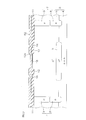
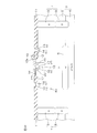
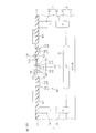
- FIG. 1 is a schematic plan view for explaining the configuration of the semiconductor device according to the first embodiment of the present invention.
- FIG. 2 is a schematic cross-sectional view taken along the line II-II of FIG.
- FIG. 3 is a schematic cross-sectional view showing an example of a simulation model relating to a comparative example.
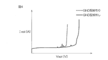
- FIG. 4 is a graph showing the simulation results for the comparative example.
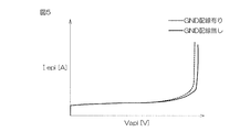
- FIG. 5 is a graph showing the simulation results for the present embodiment.
- FIG. 6A is a cross-sectional view showing an example of a manufacturing process of the semiconductor device shown in FIGS. 1 and 2, and is a cross-sectional view corresponding to the cut surface of FIG.
- FIG. 6B is a cross-sectional view showing the next step of FIG. 6A.
- FIG. 6C is a cross-sectional view showing the next step of FIG. 6B.
- FIG. 6D is a cross-sectional view showing the next step of FIG. 6C.
- FIG. 6E is a cross-sectional view showing the next step of FIG. 6D.
- FIG. 6F is a cross-sectional view showing the next step of FIG. 6E.
- FIG. 6G is a cross-sectional view showing the next step of FIG. 6F.
- FIG. 7 is a schematic plan view for explaining the configuration of the semiconductor device according to the second embodiment of the present invention.
- FIG. 10 is a schematic plan view for explaining the configuration of the semiconductor device according to the third embodiment of the present invention.
- FIG. 11 is a schematic cross-sectional view taken along the line Xl-Xl of FIG. 12A is a cross-sectional view showing an example of the manufacturing process of the semiconductor device shown in FIGS.
- FIG. 12B is a cross-sectional view showing the next step of FIG. 12A.
- FIG. 12C is a cross-sectional view showing the next step of FIG. 12B.
- FIG. 1 is a schematic plan view for explaining the configuration of the semiconductor device according to the first embodiment of the present invention.
- FIG. 2 is a schematic cross-sectional view taken along the line II-II of FIG. In FIG. 1, the interlayer insulating film 21 and the source wiring 26 shown in FIG. 2 are omitted. However, the drain wiring 25 shown in FIG. 2 is shown in FIG.
- the horizontal direction of the paper surface of FIG. 1 will be referred to as the horizontal direction
- the vertical direction of the paper surface of FIG. 1 will be referred to as the vertical direction.
- the semiconductor device 1 includes a substrate 3.
- the substrate 3 includes a p-type semiconductor substrate 4 and an n - type epitaxial layer 5 formed on the p-type semiconductor substrate 4.
- the p-type semiconductor substrate 4 is a silicon substrate.
- the p-type semiconductor substrate 4 is an example of the "p-type substrate” of the present invention
- the n - type epitaxial layer 5 is an example of the "n-type semiconductor layer" of the present invention.
- the film thickness of the n - type epitaxial layer 5 is, for example, about 3.0 ⁇ m to 10 ⁇ m.
- a p-type element separation region 7 for partitioning the element region 2 is formed on the surface layer portion of the substrate 3.
- the element region 2 has a rectangular shape that is long in the vertical direction in a plan view.
- a DMOS transistor 40 having an n- type epitaxial layer 5 as a drain is formed in the element region 2.
- the p-type element separation region film 7 is endless in a plan view.
- the p-type element separation region 7 has a rectangular ring shape in a plan view, but may have an endless shape such as an annular shape or an elliptical ring shape.
- the p-type element separation region 7 includes a lower separation region 8 connected to the p-type semiconductor substrate and an upper separation region 9 formed on the lower separation region 8.
- the substrate 3 is partitioned on the p-type semiconductor substrate 4 with an element region 2 composed of a part of the n-type epitaxial layer 5 surrounded by the p-type element separation region 7.
- the p-type element separation region 7 and the p-type semiconductor substrate 4 are grounded.
- n + type embedded layer 6 having a high value is selectively formed.
- the n + type embedded layer 6 is formed in a central region surrounded by a peripheral portion of the element region 2 in a plan view.
- the film thickness of the n + type embedded layer 6 is, for example, about 2.0 ⁇ m to 10.0 ⁇ m.
- an element region (not shown) in which an element different from the DMOS transistor 40 is formed in the element region 2 is partitioned in the outer peripheral region of the element region 2.
- An endless field insulating film 11 is formed on the surface of the p-type element separation region 7 in a plan view.
- the field insulating film 11 is formed in a square ring shape in a plan view so as to surround the region surrounded by the peripheral edge portion of the element region 2.
- the field insulating film 11 is wider than the p-type element separation region 7 and is formed so as to completely cover the p-type element separation region 7.
- the field insulating film 11 is, for example, a LOCOS film formed by selectively oxidizing the surface of the n-type epitaxial layer 5.
- the DMOS transistor 40 includes an n-type drain region 13 and a p-type well region 15 formed on the surface layer portion of the n-type epitaxial layer 5 at intervals from each other.
- the p-type well region 15 has a rectangular shape elongated in the vertical direction in a plan view, and is formed in the central portion in the horizontal direction of the element region 2.
- the n-type drain region 13 has a higher impurity concentration than that of the n-type epitaxial layer 5.
- the n-type drain region 13 is formed in an endless shape so as to surround the p-type well region 15 in a plan view.
- the n-type drain region 13 is formed in a square ring along the field insulating film 11 in a plan view.
- An n + type drain contact region 14 having a higher impurity concentration than the n-type drain region 13 is formed on the surface layer portion of the n-type drain region 13.
- n-type source region 16 having a higher impurity concentration than the n- type epitaxial layer 5 is formed on the surface layer of the p-type well region 15.
- An n + type source contact region 17 having a higher impurity concentration than the n-type source region 16 is formed on the surface layer portion of the n-type source region 16.
- the n-type source region 16 is formed, for example, at the same concentration and depth as the n-type drain region 13.
- the outer peripheral edge of the n + type source contact region 17 is arranged at a space inward from the outer peripheral edge of the p-type well region 15.
- the n + type source contact region 17 is formed, for example, at the same concentration and the same depth as the n + type drain contact region 14.
- a square annular field insulating film 12 in a plan view is formed in a portion between the n + type drain contact region 14 and the p-type well region 15.
- the field insulating film 12 is a LOCOS film formed in the same process as the above-mentioned field insulating film 11.
- the inner peripheral edge of the field insulating film 12 is indicated by reference numeral 12a.
- the inner peripheral edge 12a of the field insulating film 12 is arranged at an interval outward from the outer peripheral edge of the p-type well region 15, and the outer peripheral edge of the field insulating film 12 is placed on the inner peripheral edge of the n + type drain contact region 14. It is arranged.
- the n + type drain contact region 14 is formed in a region sandwiched between the outer peripheral edge of the field insulating film 12 and the inner peripheral edge of the field insulating film 11.
- n - the surface of the type epitaxial layer 5 n - gate insulating film 18 is formed so as to extend between the type epitaxial layer 5 and the p-type well region 15.
- the gate insulating film 18 is formed in a square ring shape so as to surround the n + type source contact region 17 in a plan view.
- the gate electrode 19 is formed on the gate insulating film 18.
- the gate electrode 19 is formed in a square ring shape so as to surround the n-type source region 16 in a plan view.
- the gate electrode 19 is formed so as to selectively cover a part of the gate insulating film 18 and a part of the field insulating film 12.
- the gate electrode 19 is made of polysilicon, for example.
- the gate insulating film 18 is, for example, a silicon oxide film formed by oxidizing the surface of the n-type epitaxial layer 5.
- the region where the gate electrode 19 faces the p-type well region 15 via the gate insulating film 18 is the channel region 20 of the DMOS transistor 40.
- the formation of channels in the channel region 20 is controlled by the gate electrode 19.
- the interlayer insulating film 21 is formed so as to cover the entire element region 2.
- the interlayer insulating film 21 is formed of, for example, an insulating film such as an oxide film or a nitride film.
- a drain contact plug 22, a source contact plug 23, and a gate contact plug 24 are embedded in the interlayer insulating film 21.
- the lower end of the drain contact plug 22 is electrically connected to the n + type drain contact region 14.
- the lower end of the source contact plug 23 is electrically connected to the n + type source contact region 17.
- the gate contact plug 24 is electrically connected to the gate electrode 19.
- a drain wiring 25, a source wiring 26, and a gate wiring are formed on the interlayer insulating film 21.
- the area of the drain wiring 25 is shown as a dot hatching area.
- the drain wiring 25 is electrically connected to the n + type drain contact region 14 via a plurality of drain contact plugs 22.
- the source wiring 26 is electrically connected to the n + type source contact region 17 via a plurality of source contact plugs 23.
- the gate wiring is electrically connected to the gate electrode 19 via a plurality of gate contact plugs 24.
- the source wiring 26 has a rectangular shape that is long in the vertical direction in a plan view and covers an intermediate length between both ends of the gate electrode 19.
- a plurality of locations at the center of the width of the source wiring 26 are electrically connected to the n + type source contact region 17 via a plurality of source contact plugs 23.
- the gate wiring is electrically connected to both ends of the gate electrode 19 via a plurality of gate contact plugs 24.
- the drain wiring 25 is formed in a square ring shape so as to surround the field insulating film 12 in a plan view.
- the inner peripheral edge of the drain wiring 25 is substantially directly above the inner peripheral edge of the n + type drain contact region 14.
- the outer peripheral edge of the drain wiring 25 is outside the outer peripheral edge of the n + type drain contact region 14.
- the drain wiring 25 includes a main wiring portion 25A arranged directly above the n + type drain contact region 14, and an extension portion 25B extending outward from the outer peripheral edge of the main wiring portion 25A.
- the extension portion 25B constitutes the "conductive wiring" of the present invention (hereinafter, may be referred to as "withstand voltage improving wiring").
- the extension portion (withstand voltage improving wiring) 25B is a square ring in a plan view, and extends from the outer peripheral edge of the n + type drain contact region 14 toward the p-type element separation region 7 outside the outer peripheral edge.
- the extension portion 25B in plan view, from the outer peripheral edge of the n + -type drain contact region 14, the inner peripheral edge of the p-type isolation region 7 the outer peripheral edge and its outer n + -type drain contact region 14 It extends almost to the center of the width between.
- the extension portion (withstand voltage improving wiring) 25B is a peripheral edge region of the element region 2, and is between the outer peripheral edge of the n + type drain contact region 14 and the inner peripheral edge of the p-type element separation region 7 outside the outer peripheral edge. It is arranged so as to cover a part of the element termination region 30.
- the extension portion 25B may extend outward from the outer peripheral edge of the n + type drain contact region 14 in a plan view. Therefore, the extension portion 25B in plan view, for example, from the outer peripheral edge of the n + -type drain contact region 14, the outer peripheral edge of the n + -type drain contact region 14 and the inner periphery of the p-type isolation region 7 of the outer It may extend to an arbitrary position between them, or may extend outward from the inner peripheral edge of the p-type element separation region 7.
- other wiring when running through the can due to the influence of the potential of the other wiring, n - -type epitaxial layer 5 and the p
- the isopotential distribution may be disturbed, and the withstand voltage may decrease. If the potential of the other wiring is the same as the potential (drain voltage) of the element region 2, the equipotential distribution is not disturbed, but if the potential of the other wiring is the ground potential, the isobaric distribution is disturbed.
- the drain wiring 25 is formed with an extension portion (withstand voltage improving wiring) 25B that covers at least a part of the element termination region 30.
- a wiring having the same potential as the element region 2 (withstand voltage improving wiring) can be obtained so as to be arranged on the element termination region 30. Therefore, even if the potential of the other wiring is the ground potential, the influence of the potential of the other wiring is obtained. Can be suppressed.
- the potential of the other wiring is the ground potential, the disturbance of the equipotential distribution can be suppressed, the decrease in the withstand voltage of the DMOS transistor 40 can be suppressed, or the withstand voltage can be improved.
- the semiconductor device 1 of FIGS. 1 and 2 is referred to as "the present embodiment", and the configuration in which the drain wiring 25 is not provided with the extension portion 25B in the semiconductor device 1 of FIGS. 1 and 2 is referred to as a "comparative example”. do. That is, in the comparative example, the drain wiring 25 is composed of only the main wiring portion 25A of the present embodiment.
- a first simulation model 101 in which a wiring 50 (hereinafter referred to as “GND wiring”) having a potential of ground potential is arranged on the element termination region 30 is used.
- the withstand voltage of the comparative example was calculated.
- the parts corresponding to FIG. 2 described above are designated by the same reference numerals as those in FIG.
- the withstand voltage of the comparative example was calculated using the second simulation model in which the GND wiring is not arranged on the element termination region 30.
- the reverse voltage applied to the parasitic diode existing between the n- type epitaxial layer 5 (n + type drain contact region 14) and the p-type element separation region 7 is defined as V epi [V]. .. Further, the reverse current flowing through the parasitic diode is defined as I epi [A]. The reverse current I epi when the reverse voltage V epi was gradually increased was calculated by simulation.
- the withstand voltage of the present embodiment was calculated using the third simulation model in which the GND wiring is arranged on the element termination region 30. Further, regarding the present embodiment, the withstand voltage of the present embodiment was calculated using the fourth simulation model in which the GND wiring is not arranged.
- FIG. 4 is a graph showing the simulation results for the comparative example.
- the broken line is a graph showing the simulation result when the GND wiring is present
- the solid line is the graph showing the simulation result when the GND wiring is not present.
- FIG. 5 is a graph showing the simulation results for this embodiment.
- the broken line is a graph showing the simulation result when the GND wiring is present
- the solid line is the graph showing the simulation result when the GND wiring is not present.
- the breakdown voltage is lower when the GND wiring is present than when the GND wiring is not present. Further, in the comparative example, the absolute value difference between the breakdown voltage when the GND wiring is present and the breakdown voltage when the GND wiring is not present is relatively large.
- the breakdown voltage when the GND wiring is present and the breakdown voltage when the GND wiring is not present are substantially equal to each other. Moreover, the breakdown voltage when the GND wiring in the present embodiment does not exist is higher than the breakdown voltage when the GND wiring does not exist in the comparative example.
- the withstand voltage when the other wiring of the ground potential exists is almost equal to the withstand voltage when the other wiring of the ground potential does not exist.
- the withstand voltage of the DMOS transistor does not decrease so much even if other wiring having a ground potential is present.
- the withstand voltage when other wiring of the ground potential is present is higher than that of the comparative example. Further, in the present embodiment, the withstand voltage when there is no other wiring of the ground potential is also higher than that of the comparative example.
- the GND wiring is present as compared with the comparative example.
- the absolute difference in breakdown voltage when it does not exist has become smaller.
- the outward protrusion amount of the extension portion (withstand voltage improving wiring) 25B When was about half of L (about 0.5 L), the withstand voltage became the largest.
- FIGS. 6A to 6G are cross-sectional views for explaining an example of the manufacturing process of the semiconductor device 1, and are cross-sectional views corresponding to the cut surface of FIG.
- a p-type semiconductor substrate 4 is prepared as shown in FIG. 6A.
- the n-type impurities and the p-type impurities are selectively injected onto the surface of the p-type semiconductor substrate 4.
- silicon is epitaxially grown on the p-type semiconductor substrate 4 while adding n-type impurities.
- FIG. 6B the substrate 3 including the p-type semiconductor substrate 4 and the n- type epitaxial layer 5 is formed.
- the n-type impurities and p-type impurities injected into the p-type semiconductor substrate 4 diffuse in the growth direction of the n-type epitaxial layer 5.
- an n + type embedded layer 6 straddling the boundary between the p-type semiconductor substrate 4 and the n - type epitaxial layer 5 and a p-type lower separation region 8 are formed.
- the p-type impurity include B (boron) and Al (aluminum)
- examples of the n-type impurity include P (phosphorus) and As (arsenic).
- an ion implantation mask (not shown) having an opening selectively in the region where the p-type upper separation region 9 should be formed is formed on the n-type epitaxial layer 5. Then, the p-type impurity is implanted into the n - type epitaxial layer 5 through the ion implantation mask. As a result, the p-type element separation region 7 having a two-layer structure of the lower separation region 8 and the upper separation region 9 is formed. After this, the ion implantation mask is removed.
- a hard mask 51 having an opening selectively in the region where the field insulating films 11 and 12 are to be formed is formed on the n - type epitaxial layer 5. Then, the surface of the n- type epitaxial layer 5 is subjected to thermal oxidation treatment via the hard mask 51 to form the field insulating films 11 and 12. After this, the hard mask 51 is removed.
- the surface of the n- type epitaxial layer 5 is subjected to thermal oxidation treatment to form the gate insulating film 18.
- the gate insulating film 18 is formed so as to be connected to the field insulating films 11 and 12.
- the polysilicon for the gate electrode 19 is deposited on the n- type epitaxial layer 5, and the polysilicon layer 52 is formed.
- a resist mask (not shown) having an opening selectively in the region where the gate electrode 19 should be formed is formed on the polysilicon layer 52. Then, an unnecessary portion of the polysilicon layer 52 is removed by etching via the resist mask. As a result, the gate electrode 19 is formed. After this, the resist mask is removed.
- a hard mask (not shown) having an opening selectively is formed on the n- type epitaxial layer 5. Then, an unnecessary portion of the gate insulating film 18 is etched through the hard mask. As a result, a predetermined gate insulating film 18 is formed. After this, the hard mask is removed. The step of selectively etching the gate insulating film 18 may be omitted.
- a p-type well region 15 is formed on the surface layer portion of the n-type epitaxial layer 5.
- an ion implantation mask (not shown) having an opening selectively in the region where the p-type well region 15 should be formed is formed.
- the p-type impurity is implanted into the n - type epitaxial layer 5 through the ion implantation mask.
- the p-type impurities are thermally diffused, for example, at a temperature of 900 ° C. to 1100 ° C.
- the ion implantation mask is removed.
- the p-type well region 15 is formed by selectively injecting p-type impurities into the n- type epitaxial layer 5 before the gate insulating film 18 and the gate electrode 19 are formed (FIG. 6C). You may.
- n - n-type source region 16 inwardly region (surface layer portion) of the p-type well region 15 and at the same time the n-type drain region 13 is formed in a surface portion of the type epitaxial layer 5 is formed.
- ion implantation having an opening selectively in each of the region where the n-type drain region 13 should be formed and the region where the n-type source region 16 should be formed.
- a mask (not shown) is formed.
- the n-type impurity is implanted into the n - type epitaxial layer 5 through the ion implantation mask.
- the n-type drain region 13 and the n-type source region 16 are formed.
- the ion implantation mask is removed.
- the n + type drain contact region 14 and the n + type source contact region 17 are selectively formed in each inner region (surface layer portion) of the n-type drain region 13 and the n-type source region 16.
- an opening is selectively opened in each of the areas where the n + type drain contact area 14 and the n + type source contact area 17 should be formed.
- An ion implantation mask (not shown) is formed.
- the n-type impurity is injected into the n-type drain region 13 and the n-type source region 16 through the ion implantation mask.
- the n + type drain contact region 14 and the n + type source contact region 17 are formed.
- the ion implantation mask is removed.
- an insulating material is deposited so as to cover the gate electrode 19, and an interlayer insulating film 21 is formed.
- the drain contact plug 22, the source contact plug 23, and the gate contact plug 24 are formed so as to penetrate the interlayer insulating film 21.
- the drain contact plug 22, the source contact plug 23, and the gate contact plug 24 are electrically connected to the n + type drain contact region 14, the n + type source contact region 17, and the gate electrode 19, respectively.
- the drain wiring 25, the source wiring 26, and the gate wiring (not shown) electrically connected to the drain contact plug 22, the source contact plug 23, and the gate contact plug 24 are placed on the interlayer insulating film 21. It is selectively formed.
- a wiring material layer is formed on the interlayer insulating film 21.
- the drain wiring 25, the source wiring 26, and the gate wiring are formed by selectively removing the wiring material layer by photolithography and etching.
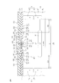
- FIG. 7 is a schematic plan view for explaining the configuration of the semiconductor device according to the second embodiment of the present invention.
- FIG. 8 is a schematic cross-sectional view taken along the line VIII-VIII of FIG. In FIG. 7, the interlayer insulating film 21, the drain wiring 25, and the source wiring 26 shown in FIG. 8 are omitted. However, the withstand voltage improving wiring 65 shown in FIG. 8 is shown in FIG. 7.
- FIG. 7 the parts corresponding to the respective parts of FIG. 1 described above are designated by the same reference numerals as those in FIG.
- FIG. 8 the portions corresponding to the respective parts of FIG. 2 described above are designated by the same reference numerals as those in FIG.
- the semiconductor device 1A according to the second embodiment has a different configuration of the withstand voltage improving wiring than the semiconductor device 1 according to the first embodiment described above.
- the withstand voltage improving wiring is configured by the extension portion 25B of the drain wiring 25.
- the withstand voltage improving wiring is provided independently of the drain wiring 25.
- the inner peripheral edge of the field insulating film 11 covering the surface of the p-type element separation region 7 is located at a position separated from the outer peripheral edge of the n + type drain contact region 14 by a certain distance in a plan view. positioned.
- N - -type epitaxial layer 5 In the region between the n-type drain region 13 and the field insulating film 11 in Heimen view, N - -type epitaxial layer 5, and at a n-type drain region 13 and spacing, N-type regions 61 are formed.
- the n-type region 61 is formed in a square ring along the field insulating film 11 so as to surround the n-type drain region 13 in a plan view.
- the impurity concentration of the n-type region 61 is substantially equal to the impurity concentration of the n-type drain region 13.
- An n + type contact region 62 for withstand voltage improving wiring having a higher impurity concentration than the n-type region 61 is formed on the surface layer portion of the n-type region 61.
- the impurity concentration of the n + type contact region 62 is substantially equal to the impurity concentration of the n + type drain contact region 14.
- a rectangular annular field insulating film 63 in a plan view is formed in a portion between the n + type contact region 62 and the n + type drain contact region 14.
- the field insulating film 63 is a LOCOS film formed in the same process as the above-mentioned field insulating films 11 and 12.
- a contact plug 64 for pressure resistance improving wiring is embedded in the interlayer insulating film 21, in addition to the drain contact plug 22, the source contact plug 23, and the gate contact plug 24, a contact plug 64 for pressure resistance improving wiring is embedded.
- the lower end of the contact plug 64 is electrically connected to the n + type contact region 62.
- the withstand voltage improving wiring 65 is formed on the interlayer insulating film 21.
- the region of the withstand voltage improving wiring 65 is shown as a dot hatching region.
- the drain wiring 25 is composed of only the main wiring portion 25A of the drain wiring 25 of the first embodiment.
- the withstand voltage improving wiring 65 is electrically connected to the n + type contact region 62 via a plurality of contact plugs 64.
- the withstand voltage improving wiring 65 is formed in a square ring shape so as to surround the field insulating film 63 in a plan view.
- the inner peripheral edge of the withstand voltage improving wiring 65 is substantially directly above the inner peripheral edge of the n + type contact region 62.
- the inner peripheral edge of the withstand voltage improving wiring 65 may be located closer to the outer peripheral edge of the n + type drain contact region 14 in a plan view.
- the outer peripheral edge of the withstand voltage improving wiring 65 is outside the outer peripheral edge of the n + type contact region 62.
- the outer peripheral edge of the withstand voltage improving wiring 65 is located between the outer peripheral edge of the n + type contact region 62 and the inner peripheral edge of the p-type element separation region 7 outside the outer peripheral edge of the n + type contact region 62 in a plan view.
- the withstand voltage improving wiring 65 is a peripheral edge region of the element region 2, and is an element termination region 30 between the outer peripheral edge of the n + type drain contact region 14 and the inner peripheral edge of the p-type element separation region 7 outside the n + type drain contact region 14. It is arranged so as to cover a part of (in this example, the middle part of the width).
- the withstand voltage improving wiring 65 that covers at least a part of the element termination region 30 is provided.
- the withstand voltage improving wiring 65 having the same potential as the element region 2 can be arranged on the element termination region 30, so that the influence of the potential of the other wiring is suppressed even when the potential of the other wiring is the ground potential. can.
- the equipotential distribution is disturbed when a reverse voltage is applied to the parasitic diode existing between the n-type epitaxial layer and the p-type element separation region 7. Can be suppressed.
- FIGS. 9A to 9E are cross-sectional views for explaining an example of the manufacturing process of the semiconductor device 1A, and are cross-sectional views corresponding to the cut surface of FIG.
- the p-type semiconductor substrate 4 is prepared in the same manner as in the manufacturing method of the semiconductor device 1 described above. Then, after the n-type impurities and the p-type impurities are selectively injected into the surface of the p-type semiconductor substrate 4, the p-type semiconductor substrate 4 is added while adding the n-type impurities, for example, in a heating environment of 1100 ° C. or higher. Impurity grow silicon on top. As a result, as shown in FIG. 6B, the substrate 3 including the p-type semiconductor substrate 4 and the n- type epitaxial layer 5 is formed. As a result, the n + type embedded layer 6 and the p-type lower separation region 8 straddling the boundary between the p-type semiconductor substrate 4 and the n -type epitaxial layer 5 are formed.
- an ion implantation mask (not shown) having an opening selectively in the region where the p-type upper separation region 9 should be formed is formed on the n-type epitaxial layer 5. Then, the p-type impurity is implanted into the n - type epitaxial layer 5 through the ion implantation mask. As a result, the p-type element separation region 7 having a two-layer structure of the lower separation region 8 and the upper separation region 9 is formed. After this, the ion implantation mask is removed.
- a hard mask 71 having an opening selectively in the region where the field insulating films 11, 12, and 63 should be formed is formed on the n - type epitaxial layer 5. Then, the surface of the n- type epitaxial layer 5 is subjected to thermal oxidation treatment via the hard mask 71 to form the field insulating films 11, 12, 63. After this, the hard mask 71 is removed.
- the surface of the n- type epitaxial layer 5 is subjected to thermal oxidation treatment to form the gate insulating film 18.
- the gate insulating film 18 is formed so as to be connected to the field insulating films 11, 63, 12.
- the polysilicon for the gate electrode 19 is deposited on the n- type epitaxial layer 5, and the polysilicon layer 72 is formed.
- a resist mask (not shown) having an opening selectively in the region where the gate electrode 19 should be formed is formed on the polysilicon layer 72. Then, an unnecessary portion of the polysilicon layer 72 is removed by etching via the resist mask. As a result, the gate electrode 19 is formed. After this, the resist mask is removed.
- a hard mask (not shown) having an opening selectively is formed on the n- type epitaxial layer 5. Then, an unnecessary portion of the gate insulating film 18 is etched through the hard mask. As a result, a predetermined gate insulating film 18 is formed. After this, the hard mask is removed. The step of selectively etching the gate insulating film 18 may be omitted.
- a p-type well region 15 is formed on the surface layer portion of the n-type epitaxial layer 5.
- an ion implantation mask (not shown) having an opening selectively in the region where the p-type well region 15 should be formed is formed.
- the p-type impurity is implanted into the n - type epitaxial layer 5 through the ion implantation mask.
- the p-type impurities are thermally diffused, for example, at a temperature of 900 ° C. to 1100 ° C.
- the ion implantation mask is removed.
- the p-type well region 15 is formed by selectively injecting p-type impurities into the n- type epitaxial layer 5 before the gate insulating film 18 and the gate electrode 19 are formed (FIG. 9A). You may.
- n - n-type source region 16 inwardly region (surface layer portion) of the p-type well region 15 and at the same time the n-type drain region 13 and the n-type region 61 is formed in a surface portion of the type epitaxial layer 5 is formed Will be done.
- the n-type drain region 13, the n-type region 61, and the n-type source region 16 are formed, for example, as follows.
- an ion implantation mask (not shown) having openings selectively in each of the region where the n-type drain region 13 should be formed, the region where the n-type region 61 should be formed, and the region where the n-type source region 16 should be formed (not shown). Is formed. Then, the n-type impurity is implanted into the n - type epitaxial layer 5 through the ion implantation mask. As a result, the n-type drain region 13, the n-type region 61, and the n-type source region 16 are formed. After this, the ion implantation mask is removed.
- the n + type drain contact region 14 is formed as follows, for example.
- an ion implantation mask (not shown) having openings selectively formed in each of the regions where the n + type drain contact region 14, the n + type contact region 62, and the n + type source contact region 17 should be formed is formed. .. Then, the n-type impurities are implanted into the n-type drain region 13, the n-type region 61, and the n-type source region 16 through the ion implantation mask. As a result, the n + type drain contact region 14, the n + type contact region 62, and the n + type source contact region 17 are formed. After this, the ion implantation mask is removed.
- an insulating material is deposited so as to cover the gate electrode 19, and an interlayer insulating film 21 is formed.
- the contact plug 64, the drain contact plug 22, the source contact plug 23, and the gate contact plug 24 are formed so as to penetrate the interlayer insulating film 21.
- the contact plug 64, the drain contact plug 22, the source contact plug 23, and the gate contact plug 24 are an n + type contact area 62, an n + type drain contact area 14, an n + type source contact area 17, and a gate electrode, respectively. Each of them is electrically connected to 19.
- the withstand voltage improving wiring 65, the drain wiring 25, the source wiring 26, and the gate wiring (not shown) that are electrically connected to the contact plug 64, the drain contact plug 22, the source contact plug 23, and the gate contact plug 24, respectively. ) Is selectively formed on the interlayer insulating film 21.
- the drain wiring 25, the source wiring 26, and the gate wiring for example, a wiring material layer is formed on the interlayer insulating film 21. Then, by selectively removing the wiring material layer by photolithography and etching, the withstand voltage improving wiring 65, the drain wiring 25, the source wiring 26, and the gate wiring are formed. Through the above steps, the semiconductor device 1A according to the second embodiment is manufactured.
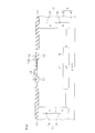
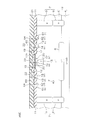
- FIG. 10 is a schematic plan view for explaining the configuration of the semiconductor device according to the third embodiment of the present invention.
- FIG. 11 is a schematic cross-sectional view taken along the line XI-XI of FIG.
- the interlayer insulating film 21, the drain wiring 25, and the source wiring 26 shown in FIG. 11 are omitted.
- the withstand voltage improving wiring 81 shown in FIG. 11 is shown in FIG.
- FIG. 10 the parts corresponding to the respective parts of FIG. 1 described above are designated by the same reference numerals as those in FIG.
- FIG. 11 the parts corresponding to the respective parts of FIG. 2 described above are designated by the same reference numerals as those in FIG.
- the semiconductor device 1B according to the third embodiment has a different configuration of the withstand voltage improving wiring than the semiconductor device 1 according to the first embodiment described above.
- the withstand voltage improving wiring is configured by the extension portion 25B of the drain wiring 25.
- the withstand voltage improving wiring is provided independently of the drain wiring 25.
- the drain wiring 25 has an extension portion 25B as in the first embodiment, and this extension portion 25B also functions as a withstand voltage improving wiring.
- the withstand voltage improving wiring 81 is formed on the field insulating film 11.
- the region of the withstand voltage improving wiring 81 is shown as a dot hatching region.
- the withstand voltage improving wiring 81 is formed in a square ring along the p-type element separation region 7 so as to surround the n + type drain contact region 14 in a plan view.
- the withstand voltage improving wiring 81 is made of polysilicon.
- the withstand voltage improving wiring 81 is covered with an interlayer insulating film 21.
- the withstand voltage improving wiring 81 is formed outward from the n + type drain contact region 14 in a plan view.
- the inner peripheral edge of the withstand voltage improving wiring 81 is located at a position separated from the n + type drain contact region 14 outward by a certain distance in a plan view.
- the inner peripheral edge of the withstand voltage improving wiring 81 may be directly above the outer peripheral edge of the n + type drain contact region 14.
- the outer peripheral edge of the withstand voltage improving wiring 81 is inside the inner peripheral edge of the p-type element separation region 7.
- the withstand voltage improving wiring 81 is a peripheral edge region of the element region 2, and is an element termination region 30 between the outer peripheral edge of the n + type drain contact region 14 and the inner peripheral edge of the p-type element separation region 7 outside the n + type drain contact region 14. It is arranged so as to cover a part of (in this example, the middle part of the width).
- the drain wiring 25 includes a main wiring portion 25A arranged directly above the n + type drain contact region 14, and an extension portion 25B extending outward from the outer peripheral edge of the main wiring portion 25A.
- the extension portion 25B has a superposed portion that overlaps the surface of the withstand voltage improving wiring 81 in a plan view.
- a plurality of contact plugs 82 for electrically connecting the superposed portion of the extension portion 25B and the withstand voltage improving wiring 81 are embedded in the interlayer insulating film 21.
- the withstand voltage improving wiring 81 is electrically connected to the drain wiring 25 via a plurality of contact plugs 82. Therefore, the withstand voltage improving wiring 81 is electrically connected to the n- type epitaxial layer 5 via the contact plug 82, the drain wiring 25, and the drain contact plug 22.
- the withstand voltage improving wiring 81 that covers at least a part of the element termination region 30 is provided.
- the withstand voltage improving wiring 81 having the same potential as the element region 2 can be arranged on the element termination region 30, so that the influence of the potential of the other wiring is suppressed even when the potential of the other wiring is the ground potential. can.
- the equipotential distribution is disturbed when a reverse voltage is applied to the parasitic diode existing between the n-type epitaxial layer and the p-type element separation region 7. Can be suppressed.
- FIGS. 12A to 12C are cross-sectional views for explaining an example of the manufacturing process of the semiconductor device 1B, and is a cross-sectional view corresponding to the cut surface of FIG.
- FIGS. 6A to 6D are applied as they are to the manufacturing method of the semiconductor device 1B.
- polysilicon is deposited on the n- type epitaxial layer 5 and the polysilicon layer 52 is formed by the step of FIG. 6D, as shown in FIG. 12A, the region where the gate electrode 19 should be formed and the withstand voltage improving wiring.
- a resist mask (not shown) having openings selectively in each region where 81 should be formed is formed on the polysilicon layer 52. Then, an unnecessary portion of the polysilicon layer 52 is removed by etching via the resist mask. As a result, the gate electrode 19 and the withstand voltage improving wiring 81 are formed at the same time. After this, the resist mask is removed.
- a hard mask (not shown) having an opening selectively is formed on the n- type epitaxial layer 5. Then, an unnecessary portion of the gate insulating film 18 is etched through the hard mask. As a result, a predetermined gate insulating film 18 is formed. After this, the hard mask is removed. The step of selectively etching the gate insulating film 18 may be omitted.
- a p-type well region 15 is formed on the surface layer portion of the n-type epitaxial layer 5.
- an ion implantation mask (not shown) having an opening selectively in the region where the p-type well region 15 should be formed is formed.
- the p-type impurity is implanted into the n - type epitaxial layer 5 through the ion implantation mask.
- the p-type impurities are thermally diffused, for example, at a temperature of 900 ° C. to 1100 ° C.
- the ion implantation mask is removed.
- the p-type well region 15 is formed by selectively injecting p-type impurities into the n- type epitaxial layer 5 before the gate insulating film 18 and the gate electrode 19 are formed (FIG. 6C). You may.
- n - n-type source region 16 inwardly region (surface layer portion) of the p-type well region 15 and at the same time the n-type drain region 13 is formed in a surface portion of the type epitaxial layer 5 is formed.
- ion implantation having an opening selectively in each of the region where the n-type drain region 13 should be formed and the region where the n-type source region 16 should be formed.
- a mask (not shown) is formed.
- the n-type impurity is implanted into the n - type epitaxial layer 5 through the ion implantation mask.
- the n-type drain region 13 and the n-type source region 16 are formed.
- the ion implantation mask is removed.
- the n + type drain contact region 14 and the n + type source contact region 17 are selectively formed in each inner region (surface layer portion) of the n-type drain region 13 and the n-type source region 16.
- an opening is selectively opened in each of the areas where the n + type drain contact area 14 and the n + type source contact area 17 should be formed.
- An ion implantation mask (not shown) is formed.
- the n-type impurity is injected into the n-type drain region 13 and the n-type source region 16 through the ion implantation mask.
- the n + type drain contact region 14 and the n + type source contact region 17 are formed.
- the ion implantation mask is removed.
- an insulating material is deposited so as to cover the gate electrode 19 and the withstand voltage improving wiring 81 to form the interlayer insulating film 21.
- the drain contact plug 22, the source contact plug 23, the gate contact plug 24, and the contact plug 82 are formed so as to penetrate the interlayer insulating film 21.
- the drain contact plug 22, the source contact plug 23, the gate contact plug 24, and the contact plug 82 are connected to the n + type drain contact area 14, the n + type source contact area 17, the gate electrode 19, and the withstand voltage improving wiring 81, respectively. Each is electrically connected.
- drain wiring 25, the source wiring 26, and the gate wiring are selectively formed on the interlayer insulating film 21.
- the drain wiring 25 is electrically connected to the drain contact plug 22 and the withstand voltage improving wiring contact plug 82.
- the source wiring 26 and the gate wiring are electrically connected to the source contact plug 23 and the gate contact plug 24, respectively.
Abstract
A semiconductor device 1 comprises: a substrate 3 including a p-type substrate 4 and an n-type semiconductor layer 5 formed in the p-type substrate 4, and including an element region 2 having a transistor 40 having a drain of the n-type semiconductor layer; a p-type element isolating region 7 formed in an upper-layer portion of the substrate so as to define the element region; and an electrically conductive wire 25B disposed over a peripheral portion of the element region and electrically connected to the n-type semiconductor layer. The transistor in the peripheral portion of the element region includes an n+-type drain contact region 14 formed in an upper-layer portion of the n-type semiconductor layer. The electrically conductive wire is disposed so as to cover at least part of an element terminal region 30 between the n+-type drain contact region and the p-type element isolating region.
Description
この発明は、DMOS(Diffused Metal Oxide Semiconductor)トランジスタ等のトランジスタを含む半導体装置およびその製造方法に関する。
The present invention relates to a semiconductor device including a transistor such as a DMOS (Diffused Metal Oxide Semiconductor) transistor and a method for manufacturing the same.
特許文献1は、素子領域を分離するp型素子分離領域(p型ウェル)と、素子領域に形成されたDMOSトランジスタを含む半導体装置を開示している。半導体装置は、p型基板のn型エピタキシャル層(n型ウェル)の表面に選択的に形成されたソース領域とドレイン領域と、ゲート酸化膜を介してシリコン基板上に形成されたゲート電極とを含む。
Patent Document 1 discloses a semiconductor device including a p-type element separation region (p-type well) for separating the element region and a DMOS transistor formed in the element region. The semiconductor device includes a source region and a drain region selectively formed on the surface of an n-type epitaxial layer (n-type well) of a p-type substrate, and a gate electrode formed on the silicon substrate via a gate oxide film. include.
特許文献1のように素子分離構造を有する半導体装置では、DMOSトランジスタは、他の素子と混載されることがある。このような半導体装置では、DMOSトランジスタに電気的に接続される配線だけでなく、当該DMOSトランジスタ以外の他の素子(以下、「他素子」という。)に電気的に接続される複数の配線(以下、「他配線」という。)が形成される。そして、複数の他配線には、対応する他素子に合わせた様々な電圧が印加される。
In a semiconductor device having an element separation structure as in Patent Document 1, a DMOS transistor may be mixedly mounted with another element. In such a semiconductor device, not only the wiring electrically connected to the DMOS transistor but also a plurality of wirings electrically connected to other elements (hereinafter, referred to as “other elements”) other than the DMOS transistor (hereinafter referred to as “other element”). Hereinafter, "other wiring") is formed. Then, various voltages suitable for the corresponding other elements are applied to the plurality of other wirings.
このため、特許文献1記載のDMOSトランジスタでは、他配線からの電位の影響によって、n型エピタキシャル層とp型素子分離領域との間に存在する寄生ダイオードに逆方向電圧が印加されたときの等電位分布が乱れ、耐圧が低下するおそれがある。
Therefore, in the DMOS transistor described in Patent Document 1, when a reverse voltage is applied to the parasitic diode existing between the n-type epitaxial layer and the p-type element separation region due to the influence of the potential from other wiring, etc. The potential distribution may be disturbed and the withstand voltage may decrease.
本発明の目的は、他配線の電位の影響による耐圧低下を抑制できる半導体装置を提供することである。
An object of the present invention is to provide a semiconductor device capable of suppressing a decrease in withstand voltage due to the influence of an electric potential of another wiring.
本発明の一実施形態は、p型基板および前記p型基板上に形成されたn型半導体層を含み、前記n型半導体層をドレインとするトランジスタを有する素子領域を含む基体と、前記素子領域を区画するように前記基体の表層部に形成されたp型素子分離領域と、前記素子領域の周縁部上に配置されかつ前記n型半導体層に電気的に接続された導電配線とを含み、前記トランジスタは、前記素子領域の周縁部において、前記n型半導体層の表層部に形成されたn型ドレインコンタクト領域を含み、前記導電配線は、前記n型ドレインコンタクト領域と前記p型素子分離領域との間の素子終端領域の少なくとも一部を覆うように配置されている、半導体装置を提供する。
One embodiment of the present invention includes a p-type substrate, an n-type semiconductor layer formed on the p-type substrate, a substrate including an element region having a transistor having the n-type semiconductor layer as a drain, and the element region. Includes a p-type element separation region formed on the surface layer portion of the substrate so as to partition the element region, and a conductive wiring arranged on the peripheral edge portion of the element region and electrically connected to the n-type semiconductor layer. The transistor includes an n-type drain contact region formed on the surface layer of the n-type semiconductor layer at the peripheral edge of the element region, and the conductive wiring includes the n-type drain contact region and the p-type element separation region. Provided is a semiconductor device arranged so as to cover at least a part of an element termination region between and.
この構成では、他配線の電位の影響による耐圧低下を抑制できる。
With this configuration, it is possible to suppress a decrease in withstand voltage due to the influence of the potential of other wiring.
本発明の一実施形態では、前記n型ドレインコンタクト領域に電気的に接続されたドレイン配線を含み、前記ドレイン配線は、平面視において、前記素子終端領域内に延びた延長部を有しており、前記導電配線は、前記延長部から構成されている。
In one embodiment of the present invention, the drain wiring is electrically connected to the n-type drain contact region, and the drain wiring has an extension portion extending into the element termination region in a plan view. , The conductive wiring is composed of the extension portion.
本発明の一実施形態では、前記n型ドレインコンタクト領域および前記ドレイン配線は、それぞれ平面視で無端状に形成されており、前記延長部は、平面視において、前記n型ドレインコンタクト領域を取り囲むように、前記ドレイン配線の全長にわたって形成されている。
In one embodiment of the present invention, the n-type drain contact region and the drain wiring are each formed in an endless shape in a plan view, and the extension portion surrounds the n-type drain contact region in a plan view. It is formed over the entire length of the drain wiring.
本発明の一実施形態では、前記素子終端領域において、前記n型半導体層の表層部に前記導電配線用のn型コンタクト領域が形成されており、前記導電配線は、前記n型コンタクト領域に導電部材を介して電気的に接続されている。
In one embodiment of the present invention, in the element termination region, an n-type contact region for the conductive wiring is formed on the surface layer portion of the n-type semiconductor layer, and the conductive wiring is conductive to the n-type contact region. It is electrically connected via a member.
本発明の一実施形態では、前記n型ドレインコンタクト領域は、平面視で無端状に形成されており、前記n型コンタクト領域および前記導電配線は、それぞれ、平面視において、前記n型ドレインコンタクト領域を取り囲むように、無端状に形成されている。
In one embodiment of the present invention, the n-type drain contact region is formed in an endless shape in a plan view, and the n-type contact region and the conductive wiring are respectively the n-type drain contact region in a plan view. It is formed in an endless shape so as to surround the.
本発明の一実施形態では、前記n型ドレインコンタクト領域に電気的に接続されたドレイン配線を含み、前記導電配線は、前記ドレイン配線に導電部材を介して電気的に接続されている。
In one embodiment of the present invention, the drain wiring is electrically connected to the n-type drain contact region, and the conductive wiring is electrically connected to the drain wiring via a conductive member.
本発明の一実施形態では、前記導電配線は、前記素子終端領域内において、前記n型半導体層上に絶縁層を介して形成されており、前記ドレイン配線は、平面視において、前記導電配線の一部に重なる重合部を有しており、前記重合部の下面と前記導電配線の上面とが前記導電部材によって電気的に接続されている。
In one embodiment of the present invention, the conductive wiring is formed on the n-type semiconductor layer via an insulating layer in the element termination region, and the drain wiring is the conductive wiring of the conductive wiring in a plan view. It has a partially overlapping overlapping portion, and the lower surface of the overlapping portion and the upper surface of the conductive wiring are electrically connected by the conductive member.
本発明の一実施形態では、前記n型ドレインコンタクト領域および前記ドレイン配線は、平面視で無端状に形成されており、前記導電配線は、平面視において、前記n型ドレインコンタクト領域を取り囲むように、無端状に形成されており、前記ドレイン配線は、その外周縁部に前記重合部を有しており、前記重合部の下面と前記導電配線の上面の内周縁部とが前記導電部材によって電気的に接続されている。
In one embodiment of the present invention, the n-type drain contact region and the drain wiring are formed in an endless shape in a plan view, and the conductive wiring surrounds the n-type drain contact region in a plan view. The drain wiring is formed in an endless shape, and the drain wiring has the polymerized portion on the outer peripheral edge portion thereof, and the lower surface of the polymerized portion and the inner peripheral edge portion of the upper surface of the conductive wiring are electrically operated by the conductive member. Is connected.
本発明の一実施形態では、前記導電配線は、ポリシリコンからなる。
In one embodiment of the present invention, the conductive wiring is made of polysilicon.
本発明の一実施形態では、平面視で前記素子領域の中央部において、前記p型基板と前記n型半導体層との境界を跨ぐようにn型埋め込み層が形成されている。
In one embodiment of the present invention, an n-type embedded layer is formed in the central portion of the element region in a plan view so as to straddle the boundary between the p-type substrate and the n-type semiconductor layer.
本発明の一実施形態では、前記p型素子分離ウェルは、平面視において、前記素子領域を取り囲む無端状に形成されており、前記n型ドレインコンタクト領域は、平面視において、前記p型素子分離ウェルに沿って無端状に形成されている。
In one embodiment of the present invention, the p-type element separation well is formed in an endless shape surrounding the element region in a plan view, and the n-type drain contact region is a p-type element separation in a plan view. It is formed endlessly along the well.
本発明の一実施形態では、前記トランジスタは、前記n型半導体層の表層部に形成されたp型ウェル領域と、前記p型ウェル領域の表層部に形成されたn型ソース領域と、前記n型ソース領域の表層部に形成され、n型不純物濃度が前記第n型ソース領域よりも高いn型ソースコンタクト領域と、前記n型半導体層の表層部に、前記p型ウェル領域を取り囲むように無端状に形成されたn型ドレイン領域とを含み、前記n型ドレインコンタクト領域は、前記n型ドレイン領域の表層部に前記p型ウェル領域を取り囲むように形成されかつn型不純物濃度が前記n型ドレイン領域よりも高い。
In one embodiment of the present invention, the transistor has a p-type well region formed on the surface layer portion of the n-type semiconductor layer, an n-type source region formed on the surface layer portion of the p-type well region, and the n-type well region. The n-type source contact region formed on the surface layer of the type source region and having a higher n-type impurity concentration than the n-type source region and the surface layer of the n-type semiconductor layer surround the p-type well region. The n-type drain contact region includes an endlessly formed n-type drain region, the n-type drain contact region is formed on the surface layer of the n-type drain region so as to surround the p-type well region, and the n-type impurity concentration is the n-type impurity concentration. Higher than the mold drain area.
本発明の一実施形態では、前記トランジスタは、前記ソースコンタクト領域および前記ドレインコンタクト領域との間のチャネル領域を覆うように形成されたゲート絶縁膜と、前記ゲート絶縁膜上に形成され、前記ゲート絶縁膜を介して前記チャネル領域に対向するゲート電極とをさらに含む。
In one embodiment of the present invention, the transistor is formed on a gate insulating film formed so as to cover a channel region between the source contact region and the drain contact region, and the gate. It further includes a gate electrode facing the channel region via an insulating film.
本発明の一実施形態では、前記n型ソースコンタクト領域に電気的に接続されたソース配線を含む。
One embodiment of the present invention includes source wiring electrically connected to the n-type source contact region.
本発明における上述の、またはさらに他の目的、特徴および効果は、添付図面を参照して次に述べる実施形態の説明により明らかにされる。
The above-mentioned or still other purposes, features and effects of the present invention will be clarified by the description of the embodiments described below with reference to the accompanying drawings.
図1は、本発明の第1実施形態に係る半導体装置の構成を説明するための図解的な平面図である。図2は、図1のII-II線に沿う図解的な断面図である。図1では、図2に示されている層間絶縁膜21およびソース配線26は、省略されている。ただし、図2に示されているドレイン配線25は、図1に図示されている。
FIG. 1 is a schematic plan view for explaining the configuration of the semiconductor device according to the first embodiment of the present invention. FIG. 2 is a schematic cross-sectional view taken along the line II-II of FIG. In FIG. 1, the interlayer insulating film 21 and the source wiring 26 shown in FIG. 2 are omitted. However, the drain wiring 25 shown in FIG. 2 is shown in FIG.
以下において、図1の紙面の左右方向を横方向といい、図1の紙面の上下方向を縦方向ということにする。
In the following, the horizontal direction of the paper surface of FIG. 1 will be referred to as the horizontal direction, and the vertical direction of the paper surface of FIG. 1 will be referred to as the vertical direction.
半導体装置1は、基体3を備えている。基体3は、p型半導体基板4およびp型半導体基板4上に形成されたn-型エピタキシャル層5を含んでいる。この実施形態では、p型半導体基板4は、シリコン基板である。p型半導体基板4は、本発明の「p型基板」の一例であり、n-型エピタキシャル層5は、本発明の「n型半導体層」の一例である。
The semiconductor device 1 includes a substrate 3. The substrate 3 includes a p-type semiconductor substrate 4 and an n - type epitaxial layer 5 formed on the p-type semiconductor substrate 4. In this embodiment, the p-type semiconductor substrate 4 is a silicon substrate. The p-type semiconductor substrate 4 is an example of the "p-type substrate" of the present invention, and the n - type epitaxial layer 5 is an example of the "n-type semiconductor layer" of the present invention.
n-型エピタキシャル層5の膜厚は、例えば、3.0μm~10μm程度である。基体3の表層部には、素子領域2を区画するp型素子分離領域7が形成されている。この実施形態では、素子領域2は、平面視において、縦方向に長い四角形状である。素子領域2には、n-型エピタキシャル層5をドレインとするDMOSトランジスタ40が形成されている。
The film thickness of the n - type epitaxial layer 5 is, for example, about 3.0 μm to 10 μm. A p-type element separation region 7 for partitioning the element region 2 is formed on the surface layer portion of the substrate 3. In this embodiment, the element region 2 has a rectangular shape that is long in the vertical direction in a plan view. A DMOS transistor 40 having an n- type epitaxial layer 5 as a drain is formed in the element region 2.
p型素子分離領域膜7は、平面視で、無端状である。この実施形態では、p型素子分離領域7は、平面視で矩形環状であるが、円環状、楕円環状等の無端状であってもよい。p型素子分離領域7は、p型半導体基板に接続された下側分離領域8と、下側分離領域8上に形成された上側分離領域9とを備えている。
The p-type element separation region film 7 is endless in a plan view. In this embodiment, the p-type element separation region 7 has a rectangular ring shape in a plan view, but may have an endless shape such as an annular shape or an elliptical ring shape. The p-type element separation region 7 includes a lower separation region 8 connected to the p-type semiconductor substrate and an upper separation region 9 formed on the lower separation region 8.
これにより、基体3には、p型半導体基板4上においてp型素子分離領域7によって取り囲まれたn-型エピタキシャル層5の一部からなる素子領域2が区画されている。図示していないが、p型素子分離領域7およびp型半導体基板4は、接地されている。
As a result, the substrate 3 is partitioned on the p-type semiconductor substrate 4 with an element region 2 composed of a part of the n-type epitaxial layer 5 surrounded by the p-type element separation region 7. Although not shown, the p-type element separation region 7 and the p-type semiconductor substrate 4 are grounded.
素子領域2において、p型半導体基板4とn-型エピタキシャル層5の境界部には、p型半導体基板4とn-型エピタキシャル層5とに跨って、n-型エピタキシャル層5よりも不純物濃度が高いn+型埋め込み層6が選択的に形成されている。n+型埋め込み層6は、平面視で、素子領域2の周縁部に囲まれた中央領域に形成されている。n+型埋め込み層6の膜厚は、例えば、2.0μm~10.0μm程度である。
In the element region 2, p-type semiconductor substrate 4 and the n - at the boundary portion of the type epitaxial layer 5, p-type semiconductor substrate 4 and the n - across -type epitaxial layer 5, n - impurity concentration than -type epitaxial layer 5 The n + type embedded layer 6 having a high value is selectively formed. The n + type embedded layer 6 is formed in a central region surrounded by a peripheral portion of the element region 2 in a plan view. The film thickness of the n + type embedded layer 6 is, for example, about 2.0 μm to 10.0 μm.
また、基体3において、素子領域2の外周領域には、素子領域2内のDMOSトランジスタ40とは異なる他の素子が形成された素子領域(図示略)が区画されている。
Further, in the substrate 3, an element region (not shown) in which an element different from the DMOS transistor 40 is formed in the element region 2 is partitioned in the outer peripheral region of the element region 2.
p型素子分離領域7の表面には、平面視で無端状のフィールド絶縁膜11が形成されている。フィールド絶縁膜11は、素子領域2の周縁部に囲まれた領域を取り囲むように平面視で四角環状に形成されている。フィールド絶縁膜11は、p型素子分離領域7よりも幅広で、p型素子分離領域7を完全に覆うように形成されている。フィールド絶縁膜11は、例えば、n-型エピタキシャル層5の表面を選択的に酸化させて形成したLOCOS膜である。
An endless field insulating film 11 is formed on the surface of the p-type element separation region 7 in a plan view. The field insulating film 11 is formed in a square ring shape in a plan view so as to surround the region surrounded by the peripheral edge portion of the element region 2. The field insulating film 11 is wider than the p-type element separation region 7 and is formed so as to completely cover the p-type element separation region 7. The field insulating film 11 is, for example, a LOCOS film formed by selectively oxidizing the surface of the n-type epitaxial layer 5.
DMOSトランジスタ40は、n-型エピタキシャル層5の表層部に、互いに間隔を空けて形成されたn型ドレイン領域13とp型ウェル領域15とを含む。この実施形態では、p型ウェル領域15は、平面視で、縦方向に細長い四角形状であり、素子領域2の横方向の中央部に形成されている。
The DMOS transistor 40 includes an n-type drain region 13 and a p-type well region 15 formed on the surface layer portion of the n-type epitaxial layer 5 at intervals from each other. In this embodiment, the p-type well region 15 has a rectangular shape elongated in the vertical direction in a plan view, and is formed in the central portion in the horizontal direction of the element region 2.
n型ドレイン領域13は、n-型エピタキシャル層5のよりも高い不純物濃度を有している。n型ドレイン領域13は、平面視において、p型ウェル領域15を取り囲むように、無端状に形成されている。この実施形態では、n型ドレイン領域13は、平面視において、フィールド絶縁膜11に沿って四角環状に形成されている。n型ドレイン領域13の表層部には、n型ドレイン領域13よりも高い不純物濃度を有するn+型ドレインコンタクト領域14が形成されている。
The n-type drain region 13 has a higher impurity concentration than that of the n-type epitaxial layer 5. The n-type drain region 13 is formed in an endless shape so as to surround the p-type well region 15 in a plan view. In this embodiment, the n-type drain region 13 is formed in a square ring along the field insulating film 11 in a plan view. An n + type drain contact region 14 having a higher impurity concentration than the n-type drain region 13 is formed on the surface layer portion of the n-type drain region 13.
p型ウェル領域15の表層部には、n-型エピタキシャル層5よりも高い不純物濃度を有するn型ソース領域16が形成されている。n型ソース領域16の表層部には、n型ソース領域16よりも高い不純物濃度を有するn+型ソースコンタクト領域17が形成されている。
An n-type source region 16 having a higher impurity concentration than the n- type epitaxial layer 5 is formed on the surface layer of the p-type well region 15. An n + type source contact region 17 having a higher impurity concentration than the n-type source region 16 is formed on the surface layer portion of the n-type source region 16.
n型ソース領域16は、例えば、n型ドレイン領域13と同一濃度および同一深さで形成されている。n+型ソースコンタクト領域17の外周縁は、p型ウェル領域15の外周縁から内側に間隔を空けて配置されている。n+型ソースコンタクト領域17は、例えば、n+型ドレインコンタクト領域14と同一濃度および同一深さで形成されている。
The n-type source region 16 is formed, for example, at the same concentration and depth as the n-type drain region 13. The outer peripheral edge of the n + type source contact region 17 is arranged at a space inward from the outer peripheral edge of the p-type well region 15. The n + type source contact region 17 is formed, for example, at the same concentration and the same depth as the n + type drain contact region 14.
n-型エピタキシャル層5の表面には、n+型ドレインコンタクト領域14とp型ウェル領域15との間部分に、平面視四角環状のフィールド絶縁膜12が形成されている。フィールド絶縁膜12は、前述のフィールド絶縁膜11と同一工程で形成されたLOCOS膜である。図1には、フィールド絶縁膜12の内周縁が、符号12aで示されている。
On the surface of the n- type epitaxial layer 5, a square annular field insulating film 12 in a plan view is formed in a portion between the n + type drain contact region 14 and the p-type well region 15. The field insulating film 12 is a LOCOS film formed in the same process as the above-mentioned field insulating film 11. In FIG. 1, the inner peripheral edge of the field insulating film 12 is indicated by reference numeral 12a.
フィールド絶縁膜12の内周縁12aは、p型ウェル領域15の外周縁から外方に間隔をあけて配置され、フィールド絶縁膜12の外周縁は、n+型ドレインコンタクト領域14の内周縁上に配置されている。n+型ドレインコンタクト領域14は、フィールド絶縁膜12の外周縁とフィールド絶縁膜11の内周縁とによって挟まれた領域に形成されている。
The inner peripheral edge 12a of the field insulating film 12 is arranged at an interval outward from the outer peripheral edge of the p-type well region 15, and the outer peripheral edge of the field insulating film 12 is placed on the inner peripheral edge of the n + type drain contact region 14. It is arranged. The n + type drain contact region 14 is formed in a region sandwiched between the outer peripheral edge of the field insulating film 12 and the inner peripheral edge of the field insulating film 11.
また、n-型エピタキシャル層5の表面には、n-型エピタキシャル層5とp型ウェル領域15との間に跨るようにゲート絶縁膜18が形成されている。ゲート絶縁膜18は、平面視で、n+型ソースコンタクト領域17を取り囲むように、四角環状に形成されている。そして、ゲート絶縁膜18上にゲート電極19が形成されている。ゲート電極19は、平面視で、n型ソース領域16を取り囲むように、四角環状に形成されている。ゲート電極19は、ゲート絶縁膜18の一部およびフィールド絶縁膜12の一部を選択的に覆うように形成されている。
Further, n - the surface of the type epitaxial layer 5, n - gate insulating film 18 is formed so as to extend between the type epitaxial layer 5 and the p-type well region 15. The gate insulating film 18 is formed in a square ring shape so as to surround the n + type source contact region 17 in a plan view. Then, the gate electrode 19 is formed on the gate insulating film 18. The gate electrode 19 is formed in a square ring shape so as to surround the n-type source region 16 in a plan view. The gate electrode 19 is formed so as to selectively cover a part of the gate insulating film 18 and a part of the field insulating film 12.
ゲート電極19は、例えば、ポリシリコンからなる。ゲート絶縁膜18は、例えば、n-型エピタキシャル層5の表面を酸化させて形成したシリコン酸化膜である。
The gate electrode 19 is made of polysilicon, for example. The gate insulating film 18 is, for example, a silicon oxide film formed by oxidizing the surface of the n-type epitaxial layer 5.
ゲート電極19がゲート絶縁膜18を介してp型ウェル領域15と対向する領域が、DMOSトランジスタ40のチャネル領域20である。チャネル領域20のチャネルの形成は、ゲート電極19によって制御される。
The region where the gate electrode 19 faces the p-type well region 15 via the gate insulating film 18 is the channel region 20 of the DMOS transistor 40. The formation of channels in the channel region 20 is controlled by the gate electrode 19.
素子領域2全体を覆うように層間絶縁膜21が形成されている。層間絶縁膜21は、例えば、酸化膜、窒化膜等の絶縁膜によって形成されている。
The interlayer insulating film 21 is formed so as to cover the entire element region 2. The interlayer insulating film 21 is formed of, for example, an insulating film such as an oxide film or a nitride film.
層間絶縁膜21には、ドレイン用コンタクトプラグ22、ソース用コンタクトプラグ23およびゲート用コンタクトプラグ24が埋設されている。ドレイン用コンタクトプラグ22の下端は、n+型ドレインコンタクト領域14と電気的に接続されている。ソース用コンタクトプラグ23の下端は、n+型ソースコンタクト領域17と電気的に接続されている。ゲート用コンタクトプラグ24は、ゲート電極19に電気的に接続されている。
A drain contact plug 22, a source contact plug 23, and a gate contact plug 24 are embedded in the interlayer insulating film 21. The lower end of the drain contact plug 22 is electrically connected to the n + type drain contact region 14. The lower end of the source contact plug 23 is electrically connected to the n + type source contact region 17. The gate contact plug 24 is electrically connected to the gate electrode 19.
層間絶縁膜21上には、ドレイン配線25、ソース配線26およびゲート配線(図示略)が形成されている。図1においては、ドレイン配線25の領域が、ドットのハッチング領域として示されている。ドレイン配線25は、複数のドレイン用コンタクトプラグ22を介してn+型ドレインコンタクト領域14に電気的に接続されている。ソース配線26は、複数のソース用コンタクトプラグ23を介してn+型ソースコンタクト領域17に電気的に接続されている。ゲート配線は、複数のゲート用コンタクトプラグ24を介してゲート電極19に電気的に接続されている。
A drain wiring 25, a source wiring 26, and a gate wiring (not shown) are formed on the interlayer insulating film 21. In FIG. 1, the area of the drain wiring 25 is shown as a dot hatching area. The drain wiring 25 is electrically connected to the n + type drain contact region 14 via a plurality of drain contact plugs 22. The source wiring 26 is electrically connected to the n + type source contact region 17 via a plurality of source contact plugs 23. The gate wiring is electrically connected to the gate electrode 19 via a plurality of gate contact plugs 24.
ソース配線26は、図1には描かれていないが、平面視で、縦方向に長い四角形状であり、ゲート電極19の両端部の間の長さ中間部を覆っている。ソース配線26の幅中央部の複数個所が、複数のソース用コンタクトプラグ23を介してn+型ソースコンタクト領域17に電気的に接続されている。ゲート配線は、ゲート電極19の両端部に複数のゲート用コンタクトプラグ24を介して電気的に接続されている。
Although not drawn in FIG. 1, the source wiring 26 has a rectangular shape that is long in the vertical direction in a plan view and covers an intermediate length between both ends of the gate electrode 19. A plurality of locations at the center of the width of the source wiring 26 are electrically connected to the n + type source contact region 17 via a plurality of source contact plugs 23. The gate wiring is electrically connected to both ends of the gate electrode 19 via a plurality of gate contact plugs 24.
ドレイン配線25は、平面視で、フィールド絶縁膜12を取り囲むように、四角環状に形成されている。ドレイン配線25の内周縁は、n+型ドレインコンタクト領域14の内周縁のほぼ真上にある。ドレイン配線25の外周縁は、n+型ドレインコンタクト領域14の外周縁よりも外方にある。ドレイン配線25は、n+型ドレインコンタクト領域14の真上に配置された主配線部25Aと、主配線部25Aの外周縁から外方に延びた延長部25Bとからなる。第1実施形態においては、この延長部25Bが、本発明の「導電配線」(以下、「耐圧改善配線」という場合がある。)を構成している。
The drain wiring 25 is formed in a square ring shape so as to surround the field insulating film 12 in a plan view. The inner peripheral edge of the drain wiring 25 is substantially directly above the inner peripheral edge of the n + type drain contact region 14. The outer peripheral edge of the drain wiring 25 is outside the outer peripheral edge of the n + type drain contact region 14. The drain wiring 25 includes a main wiring portion 25A arranged directly above the n + type drain contact region 14, and an extension portion 25B extending outward from the outer peripheral edge of the main wiring portion 25A. In the first embodiment, the extension portion 25B constitutes the "conductive wiring" of the present invention (hereinafter, may be referred to as "withstand voltage improving wiring").
延長部(耐圧改善配線)25Bは、平面視において、四角環状であり、n+型ドレインコンタクト領域14の外周縁からその外側のp型素子分離領域7に向かって延びている。この実施形態では、延長部25Bは、平面視において、n+型ドレインコンタクト領域14の外周縁から、n+型ドレインコンタクト領域14の外周縁とその外側のp型素子分離領域7の内周縁との間のほぼ幅中央まで延びている。
The extension portion (withstand voltage improving wiring) 25B is a square ring in a plan view, and extends from the outer peripheral edge of the n + type drain contact region 14 toward the p-type element separation region 7 outside the outer peripheral edge. In this embodiment, the extension portion 25B in plan view, from the outer peripheral edge of the n + -type drain contact region 14, the inner peripheral edge of the p-type isolation region 7 the outer peripheral edge and its outer n + -type drain contact region 14 It extends almost to the center of the width between.
つまり、延長部(耐圧改善配線)25Bは、素子領域2の周縁部領域であって、n+型ドレインコンタクト領域14の外周縁とその外側のp型素子分離領域7の内周縁との間の素子終端領域30の一部を覆うように配置されている。
That is, the extension portion (withstand voltage improving wiring) 25B is a peripheral edge region of the element region 2, and is between the outer peripheral edge of the n + type drain contact region 14 and the inner peripheral edge of the p-type element separation region 7 outside the outer peripheral edge. It is arranged so as to cover a part of the element termination region 30.
延長部25Bは、平面視において、n+型ドレインコンタクト領域14の外周縁よりも外方に延びていればよい。したがって、延長部25Bは、平面視において、例えば、n+型ドレインコンタクト領域14の外周縁から、n+型ドレインコンタクト領域14の外周縁とその外側のp型素子分離領域7の内周縁との間の任意位置まで延びていてもよいし、p型素子分離領域7の内周縁よりも外方に延びていてもよい。
The extension portion 25B may extend outward from the outer peripheral edge of the n + type drain contact region 14 in a plan view. Therefore, the extension portion 25B in plan view, for example, from the outer peripheral edge of the n + -type drain contact region 14, the outer peripheral edge of the n + -type drain contact region 14 and the inner periphery of the p-type isolation region 7 of the outer It may extend to an arbitrary position between them, or may extend outward from the inner peripheral edge of the p-type element separation region 7.
素子領域2の上方にDMOSトランジスタ40以外の他の素子の配線(以下、「他配線」という。)が通っている場合には、他配線の電位の影響によって、n-型エピタキシャル層5とp型素子分離領域7との間に存在する寄生ダイオードに逆方向電圧が印加されたときの等電位分布が乱れて、耐圧が低下するおそれがある。他配線の電位が素子領域2の電位(ドレイン電圧)と同じであれば前記等電位分布は乱れないが、他配線の電位が接地電位である場合には前記等電位分布が乱れる。
Above the other elements other than the DMOS transistor 40 lines of the device region 2 (. Hereinafter referred to as "other wiring") when running through the can due to the influence of the potential of the other wiring, n - -type epitaxial layer 5 and the p When a reverse voltage is applied to the parasitic diode existing between the mold element separation region 7, the isopotential distribution may be disturbed, and the withstand voltage may decrease. If the potential of the other wiring is the same as the potential (drain voltage) of the element region 2, the equipotential distribution is not disturbed, but if the potential of the other wiring is the ground potential, the isobaric distribution is disturbed.
この実施形態では、素子終端領域30の少なくとも一部を覆う延長部(耐圧改善配線)25Bをドレイン配線25に形成している。これにより、素子領域2と同じ電位の配線(耐圧改善配線)が素子終端領域30上に配置された構成が得られるので、他配線の電位が接地電位である場合でも、他配線の電位の影響を抑制できる。これにより、他配線の電位が接地電位である場合に、前記等電位分布の乱れを抑制でき、DMOSトランジスタ40の耐圧の低下を抑制できるかまたは耐圧を向上させることができる。
In this embodiment, the drain wiring 25 is formed with an extension portion (withstand voltage improving wiring) 25B that covers at least a part of the element termination region 30. As a result, a wiring having the same potential as the element region 2 (withstand voltage improving wiring) can be obtained so as to be arranged on the element termination region 30. Therefore, even if the potential of the other wiring is the ground potential, the influence of the potential of the other wiring is obtained. Can be suppressed. As a result, when the potential of the other wiring is the ground potential, the disturbance of the equipotential distribution can be suppressed, the decrease in the withstand voltage of the DMOS transistor 40 can be suppressed, or the withstand voltage can be improved.
図1および図2の半導体装置1を「本実施形態」といい、図1および図2の半導体装置1において、ドレイン配線25に延長部25Bが設けられてない構成を「比較例」ということにする。つまり、比較例では、ドレイン配線25は、本実施形態の主配線部25Aのみから構成されている。
The semiconductor device 1 of FIGS. 1 and 2 is referred to as "the present embodiment", and the configuration in which the drain wiring 25 is not provided with the extension portion 25B in the semiconductor device 1 of FIGS. 1 and 2 is referred to as a "comparative example". do. That is, in the comparative example, the drain wiring 25 is composed of only the main wiring portion 25A of the present embodiment.
まず、図3に示すように、比較例に関して、素子終端領域30上に電位が接地電位の他配線50(以下、「GND配線」という。)が配置された第1シミュレーションモデル101を用いて、比較例の耐圧を計算した。図3において、前述の図2に対応する各部には、図2と同じ符号を付して示す。また、比較例に関して、素子終端領域30上にGND配線が配置されていない第2シミュレーションモデルを用いて、比較例の耐圧を計算した。
First, as shown in FIG. 3, for a comparative example, a first simulation model 101 in which a wiring 50 (hereinafter referred to as “GND wiring”) having a potential of ground potential is arranged on the element termination region 30 is used. The withstand voltage of the comparative example was calculated. In FIG. 3, the parts corresponding to FIG. 2 described above are designated by the same reference numerals as those in FIG. Further, regarding the comparative example, the withstand voltage of the comparative example was calculated using the second simulation model in which the GND wiring is not arranged on the element termination region 30.
具体的には、n-型エピタキシャル層5(n+型ドレインコンタクト領域14)とp型素子分離領域7との間に存在する寄生ダイオードに印加される逆方向電圧をVepi[V]とする。また、寄生ダイオードに流れる逆方向電流をIepi[A]とする。逆方向電圧Vepiを徐々に上げていったときの逆方向電流Iepiをシミュレーションによって計算した。
Specifically, the reverse voltage applied to the parasitic diode existing between the n- type epitaxial layer 5 (n + type drain contact region 14) and the p-type element separation region 7 is defined as V epi [V]. .. Further, the reverse current flowing through the parasitic diode is defined as I epi [A]. The reverse current I epi when the reverse voltage V epi was gradually increased was calculated by simulation.
同様に、本実施形態に関して、素子終端領域30上にGND配線が配置された第3シミュレーションモデルを用いて、本実施形態の耐圧を計算した。また、本実施形態に関して、GND配線が配置されていない第4シミュレーションモデルを用いて、本実施形態の耐圧を計算した。
Similarly, with respect to the present embodiment, the withstand voltage of the present embodiment was calculated using the third simulation model in which the GND wiring is arranged on the element termination region 30. Further, regarding the present embodiment, the withstand voltage of the present embodiment was calculated using the fourth simulation model in which the GND wiring is not arranged.
図4は、比較例に対するシミュレーション結果を示すグラフである。図4において、破線は、GND配線が存在する場合のシミュレーション結果を示すグラフであり、実線は、GND配線が存在しない場合のシミュレーション結果を示すグラフである。
FIG. 4 is a graph showing the simulation results for the comparative example. In FIG. 4, the broken line is a graph showing the simulation result when the GND wiring is present, and the solid line is the graph showing the simulation result when the GND wiring is not present.
図5は、本実施形態に対するシミュレーション結果を示すグラフである。図5において、破線は、GND配線が存在する場合のシミュレーション結果を示すグラフであり、実線は、GND配線が存在しない場合のシミュレーション結果を示すグラフである。
FIG. 5 is a graph showing the simulation results for this embodiment. In FIG. 5, the broken line is a graph showing the simulation result when the GND wiring is present, and the solid line is the graph showing the simulation result when the GND wiring is not present.
図4を参照して、比較例では、GND配線が存在する場合にはGND配線が存在しない場合に比べてブレークダウン電圧は低い。また、比較例では、GND配線が存在する場合のブレークダウン電圧と、GND配線が存在しない場合のブレークダウン電圧との絶対値差は比較的大きい。
With reference to FIG. 4, in the comparative example, the breakdown voltage is lower when the GND wiring is present than when the GND wiring is not present. Further, in the comparative example, the absolute value difference between the breakdown voltage when the GND wiring is present and the breakdown voltage when the GND wiring is not present is relatively large.
一方、図5を参照して、本実施形態では、GND配線が存在する場合のブレークダウン電圧と、GND配線が存在しない場合のブレークダウン電圧とはほぼ等しくなっている。しかも、本実施形態におけるGND配線が存在しない場合のブレークダウン電圧は、比較例におけるGND配線が存在しない場合のブレークダウン電圧よりも高くなっている。
On the other hand, referring to FIG. 5, in the present embodiment, the breakdown voltage when the GND wiring is present and the breakdown voltage when the GND wiring is not present are substantially equal to each other. Moreover, the breakdown voltage when the GND wiring in the present embodiment does not exist is higher than the breakdown voltage when the GND wiring does not exist in the comparative example.
つまり、本実施形態では、接地電位の他配線が存在する場合の耐圧は、接地電位の他配線が存在しない場合の耐圧とほぼ等しい。言い換えれば、本実施形態では、接地電位の他配線が存在しても、DMOSトランジスタの耐圧はさほど低下しない。
That is, in the present embodiment, the withstand voltage when the other wiring of the ground potential exists is almost equal to the withstand voltage when the other wiring of the ground potential does not exist. In other words, in the present embodiment, the withstand voltage of the DMOS transistor does not decrease so much even if other wiring having a ground potential is present.
また、本実施形態では、接地電位の他配線が存在する場合の耐圧は、比較例に比べて高くなる。さらに、本実施形態では、接地電位の他配線が存在しない場合の耐圧も、比較例に比べて高くなる。
Further, in the present embodiment, the withstand voltage when other wiring of the ground potential is present is higher than that of the comparative example. Further, in the present embodiment, the withstand voltage when there is no other wiring of the ground potential is also higher than that of the comparative example.
なお、本実施形態の延長部(耐圧改善配線)25Bの外方突出量を変化させて、同様なシミュレーションを行った結果、いずれの場合でも、比較例に比べて、GND配線が存在する場合と存在しない場合のブレークダウン電圧の絶対値差は小さくなった。また、平面視において、n+型ドレインコンタクト領域14の外周縁とその外側のp型素子分離領域7の内周縁までの距離をLとすると、延長部(耐圧改善配線)25Bの外方突出量がLの半分程度(0.5L程度)のときに、耐圧が最も大きくなった。
As a result of performing the same simulation by changing the outward protrusion amount of the extension portion (voltage improving wiring) 25B of the present embodiment, in each case, the GND wiring is present as compared with the comparative example. The absolute difference in breakdown voltage when it does not exist has become smaller. Further, in a plan view, assuming that the distance between the outer peripheral edge of the n + type drain contact region 14 and the inner peripheral edge of the p-type element separation region 7 outside the n + type drain contact region 14 is L, the outward protrusion amount of the extension portion (withstand voltage improving wiring) 25B. When was about half of L (about 0.5 L), the withstand voltage became the largest.
次に、図6A~図6Gを参照して、半導体装置1の製造工程について説明する。図6A~図6Gは、半導体装置1の製造工程の一例を説明するための断面図であって、図2の切断面に対応する断面図である。
Next, the manufacturing process of the semiconductor device 1 will be described with reference to FIGS. 6A to 6G. 6A to 6G are cross-sectional views for explaining an example of the manufacturing process of the semiconductor device 1, and are cross-sectional views corresponding to the cut surface of FIG.
半導体装置1を製造するには、図6Aに示すように、p型半導体基板4が用意される。次に、p型半導体基板4の表面にn型不純物とp型不純物とが選択的に注入される。そして、例えば1100℃以上の加熱状態下で、n型不純物を添加しながらp型半導体基板4の上にシリコンをエピタキシャル成長させる。これにより、図6Bに示すように、p型半導体基板4とn-型エピタキシャル層5とを含む基体3が形成される。
To manufacture the semiconductor device 1, a p-type semiconductor substrate 4 is prepared as shown in FIG. 6A. Next, the n-type impurities and the p-type impurities are selectively injected onto the surface of the p-type semiconductor substrate 4. Then, for example, under a heating state of 1100 ° C. or higher, silicon is epitaxially grown on the p-type semiconductor substrate 4 while adding n-type impurities. As a result, as shown in FIG. 6B, the substrate 3 including the p-type semiconductor substrate 4 and the n- type epitaxial layer 5 is formed.
エピタキシャル成長に際して、p型半導体基板4に注入されたn型不純物およびp型不純物は、n-型エピタキシャル層5の成長方向に拡散する。これにより、p型半導体基板4とn-型エピタキシャル層5との境界を跨ぐn+型埋め込み層6と、p型の下側分離領域8とが形成される。なお、p型不純物としては、例えば、B(ホウ素),Al(アルミニウム)等を挙げることができ、n型不純物としては、例えば、P(リン),As(砒素)等を挙げることができる。
During epitaxial growth, the n-type impurities and p-type impurities injected into the p-type semiconductor substrate 4 diffuse in the growth direction of the n-type epitaxial layer 5. As a result, an n + type embedded layer 6 straddling the boundary between the p-type semiconductor substrate 4 and the n - type epitaxial layer 5 and a p-type lower separation region 8 are formed. Examples of the p-type impurity include B (boron) and Al (aluminum), and examples of the n-type impurity include P (phosphorus) and As (arsenic).
次に、図6Cに示すように、p型の上側分離領域9を形成すべき領域に選択的に開口を有するイオン注入マスク(図示略)がn-型エピタキシャル層5上に形成される。そして、当該イオン注入マスクを介してp型不純物がn-型エピタキシャル層5に注入される。これにより、下側分離領域8と上側分離領域9との2層構造からなるp型素子分離領域7が形成される。この後、イオン注入マスクは除去される。
Next, as shown in FIG. 6C, an ion implantation mask (not shown) having an opening selectively in the region where the p-type upper separation region 9 should be formed is formed on the n-type epitaxial layer 5. Then, the p-type impurity is implanted into the n - type epitaxial layer 5 through the ion implantation mask. As a result, the p-type element separation region 7 having a two-layer structure of the lower separation region 8 and the upper separation region 9 is formed. After this, the ion implantation mask is removed.
次に、フィールド絶縁膜11,12を形成すべき領域に選択的に開口を有するハードマスク51がn-型エピタキシャル層5上に形成される。そして、ハードマスク51を介してn-型エピタキシャル層5の表面に熱酸化処理が施されてフィールド絶縁膜11,12が形成される。この後、ハードマスク51は除去される。
Next, a hard mask 51 having an opening selectively in the region where the field insulating films 11 and 12 are to be formed is formed on the n - type epitaxial layer 5. Then, the surface of the n- type epitaxial layer 5 is subjected to thermal oxidation treatment via the hard mask 51 to form the field insulating films 11 and 12. After this, the hard mask 51 is removed.
次に、図6Dに示すように、n-型エピタキシャル層5の表面に熱酸化処理が施されてゲート絶縁膜18が形成される。このとき、ゲート絶縁膜18はフィールド絶縁膜11,12と連なるように形成される。次に、ゲート電極19用のポリシリコンがn-型エピタキシャル層5上に堆積されて、ポリシリコン層52が形成される。
Next, as shown in FIG. 6D, the surface of the n- type epitaxial layer 5 is subjected to thermal oxidation treatment to form the gate insulating film 18. At this time, the gate insulating film 18 is formed so as to be connected to the field insulating films 11 and 12. Next, the polysilicon for the gate electrode 19 is deposited on the n- type epitaxial layer 5, and the polysilicon layer 52 is formed.
次に、図6Eに示すように、ゲート電極19を形成すべき領域に選択的に開口を有するレジストマスク(図示略)がポリシリコン層52上に形成される。そして、当該レジストマスクを介してポリシリコン層52の不要な部分がエッチングによって除去される。これにより、ゲート電極19が形成される。この後、レジストマスクは除去される。
Next, as shown in FIG. 6E, a resist mask (not shown) having an opening selectively in the region where the gate electrode 19 should be formed is formed on the polysilicon layer 52. Then, an unnecessary portion of the polysilicon layer 52 is removed by etching via the resist mask. As a result, the gate electrode 19 is formed. After this, the resist mask is removed.
次に、ゲート絶縁膜18の不要な部分を除去するため、選択的に開口を有するハードマスク(図示略)がn-型エピタキシャル層5上に形成される。そして、当該ハードマスクを介してゲート絶縁膜18の不要な部分にエッチング処理が施される。これにより、所定のゲート絶縁膜18が形成される。この後、ハードマスクは除去される。なお、このゲート絶縁膜18を選択的にエッチングする工程を省略してもよい。
Next, in order to remove an unnecessary portion of the gate insulating film 18, a hard mask (not shown) having an opening selectively is formed on the n- type epitaxial layer 5. Then, an unnecessary portion of the gate insulating film 18 is etched through the hard mask. As a result, a predetermined gate insulating film 18 is formed. After this, the hard mask is removed. The step of selectively etching the gate insulating film 18 may be omitted.
次に、図6Fに示すように、n-型エピタキシャル層5の表層部にp型ウェル領域15が形成される。p型ウェル領域15を形成するには、まず、p型ウェル領域15を形成すべき領域に選択的に開口を有するイオン注入マスク(図示略)が形成される。そして、当該イオン注入マスクを介してp型不純物がn-型エピタキシャル層5に注入される。この後、例えば900℃~1100℃の温度で、p型不純物が熱拡散される。これにより、p型ウェル領域15が形成される。この後、イオン注入マスクは、除去される。
Next, as shown in FIG. 6F, a p-type well region 15 is formed on the surface layer portion of the n-type epitaxial layer 5. In order to form the p-type well region 15, first, an ion implantation mask (not shown) having an opening selectively in the region where the p-type well region 15 should be formed is formed. Then, the p-type impurity is implanted into the n - type epitaxial layer 5 through the ion implantation mask. After that, the p-type impurities are thermally diffused, for example, at a temperature of 900 ° C. to 1100 ° C. As a result, the p-type well region 15 is formed. After this, the ion implantation mask is removed.
なお、ゲート絶縁膜18およびゲート電極19が形成される前(図6C)の段階で、p型不純物をn-型エピタキシャル層5に選択的に注入することにより、p型ウェル領域15を形成してもよい。
The p-type well region 15 is formed by selectively injecting p-type impurities into the n- type epitaxial layer 5 before the gate insulating film 18 and the gate electrode 19 are formed (FIG. 6C). You may.
次に、n-型エピタキシャル層5の表層部にn型ドレイン領域13が形成されると同時にp型ウェル領域15の内方領域(表層部)にn型ソース領域16が形成される。n型ドレイン領域13およびn型ソース領域16を形成するには、まず、n型ドレイン領域13を形成すべき領域およびn型ソース領域16を形成すべき領域それぞれに選択的に開口を有するイオン注入マスク(図示略)が形成される。そして、当該イオン注入マスクを介してn型不純物がn-型エピタキシャル層5に注入される。これにより、n型ドレイン領域13とn型ソース領域16とが形成される。この後、イオン注入マスクは、除去される。
Then, n - n-type source region 16 inwardly region (surface layer portion) of the p-type well region 15 and at the same time the n-type drain region 13 is formed in a surface portion of the type epitaxial layer 5 is formed. In order to form the n-type drain region 13 and the n-type source region 16, first, ion implantation having an opening selectively in each of the region where the n-type drain region 13 should be formed and the region where the n-type source region 16 should be formed. A mask (not shown) is formed. Then, the n-type impurity is implanted into the n - type epitaxial layer 5 through the ion implantation mask. As a result, the n-type drain region 13 and the n-type source region 16 are formed. After this, the ion implantation mask is removed.
次に、n型ドレイン領域13およびn型ソース領域16の各内方領域(表層部)にn+型ドレインコンタクト領域14およびn+型ソースコンタクト領域17がそれぞれ選択的に形成される。n+型ドレインコンタクト領域14およびn+型ソースコンタクト領域17を形成するには、まず、n+型ドレインコンタクト領域14およびn+型ソースコンタクト領域17を形成すべき領域それぞれに選択的に開口を有するイオン注入マスク(図示略)が形成される。そして、当該イオン注入マスクを介してn型不純物がn型ドレイン領域13およびn型ソース領域16に注入される。これにより、n+型ドレインコンタクト領域14およびn+型ソースコンタクト領域17が形成される。この後、イオン注入マスクは、除去される。
Next, the n + type drain contact region 14 and the n + type source contact region 17 are selectively formed in each inner region (surface layer portion) of the n-type drain region 13 and the n-type source region 16. In order to form the n + type drain contact area 14 and the n + type source contact area 17, first, an opening is selectively opened in each of the areas where the n + type drain contact area 14 and the n + type source contact area 17 should be formed. An ion implantation mask (not shown) is formed. Then, the n-type impurity is injected into the n-type drain region 13 and the n-type source region 16 through the ion implantation mask. As a result, the n + type drain contact region 14 and the n + type source contact region 17 are formed. After this, the ion implantation mask is removed.
次に、図6Gに示すように、ゲート電極19を覆うように絶縁材料が堆積されて層間絶縁膜21が形成される。次に、層間絶縁膜21を貫通するように、ドレイン用コンタクトプラグ22、ソース用コンタクトプラグ23およびゲート用コンタクトプラグ24が形成される。ドレイン用コンタクトプラグ22、ソース用コンタクトプラグ23およびゲート用コンタクトプラグ24は、それぞれ、n+型ドレインコンタクト領域14、n+型ソースコンタクト領域17およびゲート電極19にそれぞれ電気的に接続される。
Next, as shown in FIG. 6G, an insulating material is deposited so as to cover the gate electrode 19, and an interlayer insulating film 21 is formed. Next, the drain contact plug 22, the source contact plug 23, and the gate contact plug 24 are formed so as to penetrate the interlayer insulating film 21. The drain contact plug 22, the source contact plug 23, and the gate contact plug 24 are electrically connected to the n + type drain contact region 14, the n + type source contact region 17, and the gate electrode 19, respectively.
最後に、ドレイン用コンタクトプラグ22、ソース用コンタクトプラグ23およびゲート用コンタクトプラグ24それぞれに電気的に接続されるドレイン配線25、ソース配線26およびゲート配線(図示略)が、層間絶縁膜21上に選択的に形成される。ドレイン配線25、ソース配線26およびゲート配線を形成するには、例えば、層間絶縁膜21上に配線材料層を形成する。そして、フォトリソグラフィおよびエッチングによって、配線材料層を選択的に除去することにより、ドレイン配線25、ソース配線26およびゲート配線が形成される。以上の工程を経て、第1実施形態に係る半導体装置1が製造される。
Finally, the drain wiring 25, the source wiring 26, and the gate wiring (not shown) electrically connected to the drain contact plug 22, the source contact plug 23, and the gate contact plug 24 are placed on the interlayer insulating film 21. It is selectively formed. To form the drain wiring 25, the source wiring 26, and the gate wiring, for example, a wiring material layer is formed on the interlayer insulating film 21. Then, the drain wiring 25, the source wiring 26, and the gate wiring are formed by selectively removing the wiring material layer by photolithography and etching. Through the above steps, the semiconductor device 1 according to the first embodiment is manufactured.
次に、図7および図8を参照して、本発明の第2実施形態に係る半導体装置1Aについて説明する。図7は、本発明の第2実施形態に係る半導体装置の構成を説明するための図解的な平面図である。図8は、図7のVIII-VIII線に沿う図解的な断面図である。図7では、図8に示されている層間絶縁膜21、ドレイン配線25およびソース配線26は、省略されている。ただし、図8に示されている耐圧改善配線65は、図7に図示されている。
Next, the semiconductor device 1A according to the second embodiment of the present invention will be described with reference to FIGS. 7 and 8. FIG. 7 is a schematic plan view for explaining the configuration of the semiconductor device according to the second embodiment of the present invention. FIG. 8 is a schematic cross-sectional view taken along the line VIII-VIII of FIG. In FIG. 7, the interlayer insulating film 21, the drain wiring 25, and the source wiring 26 shown in FIG. 8 are omitted. However, the withstand voltage improving wiring 65 shown in FIG. 8 is shown in FIG. 7.
図7において、前述の図1の各部に対応する部分には図1と同じ符号を付して示す。図8において、前述の図2の各部に対応する部分には図2と同じ符号を付して示す。
In FIG. 7, the parts corresponding to the respective parts of FIG. 1 described above are designated by the same reference numerals as those in FIG. In FIG. 8, the portions corresponding to the respective parts of FIG. 2 described above are designated by the same reference numerals as those in FIG.
第2実施形態に係る半導体装置1Aでは、前述の第1実施形態に係る半導体装置1に比べて、耐圧改善配線の構成が異なっている。第1実施形態に係る半導体装置1では、ドレイン配線25の延長部25Bによって耐圧改善配線が構成されている。第2実施形態に係る半導体装置1Aでは、ドレイン配線25とは別に、独立して耐圧改善配線が設けられている。
The semiconductor device 1A according to the second embodiment has a different configuration of the withstand voltage improving wiring than the semiconductor device 1 according to the first embodiment described above. In the semiconductor device 1 according to the first embodiment, the withstand voltage improving wiring is configured by the extension portion 25B of the drain wiring 25. In the semiconductor device 1A according to the second embodiment, the withstand voltage improving wiring is provided independently of the drain wiring 25.
第2実施形態では、p型素子分離領域7の表面を覆うフィールド絶縁膜11の内周縁は、平面視で、n+型ドレインコンタクト領域14の外周縁から外方に一定距離だけ離れた位置に位置している。
In the second embodiment, the inner peripheral edge of the field insulating film 11 covering the surface of the p-type element separation region 7 is located at a position separated from the outer peripheral edge of the n + type drain contact region 14 by a certain distance in a plan view. positioned.
平面視でn型ドレイン領域13とフィールド絶縁膜11との間の領域において、n-型エピタキシャル層5には、n型ドレイン領域13と間隔をおいて、n型領域61が形成されている。
In the region between the n-type drain region 13 and the field insulating film 11 in Heimen view, N - -type epitaxial layer 5, and at a n-type drain region 13 and spacing, N-type regions 61 are formed.
n型領域61は、平面視において、n型ドレイン領域13を取り囲むように、フィールド絶縁膜11に沿って四角環状に形成されている。n型領域61の不純物濃度は、n型ドレイン領域13の不純物濃度とほぼ等しい。n型領域61の表層部には、n型領域61よりも高い不純物濃度を有する耐圧改善配線用のn+型コンタクト領域62が形成されている。n+型コンタクト領域62の不純物濃度は、n+型ドレインコンタクト領域14の不純物濃度とほぼ等しい。
The n-type region 61 is formed in a square ring along the field insulating film 11 so as to surround the n-type drain region 13 in a plan view. The impurity concentration of the n-type region 61 is substantially equal to the impurity concentration of the n-type drain region 13. An n + type contact region 62 for withstand voltage improving wiring having a higher impurity concentration than the n-type region 61 is formed on the surface layer portion of the n-type region 61. The impurity concentration of the n + type contact region 62 is substantially equal to the impurity concentration of the n + type drain contact region 14.
n-型エピタキシャル層5の表面には、n+型コンタクト領域62とn+型ドレインコンタクト領域14との間の部分に、平面視四角環状のフィールド絶縁膜63が形成されている。フィールド絶縁膜63は、前述のフィールド絶縁膜11,12と同一工程で形成されたLOCOS膜である。
On the surface of the n- type epitaxial layer 5, a rectangular annular field insulating film 63 in a plan view is formed in a portion between the n + type contact region 62 and the n + type drain contact region 14. The field insulating film 63 is a LOCOS film formed in the same process as the above-mentioned field insulating films 11 and 12.
層間絶縁膜21には、ドレイン用コンタクトプラグ22、ソース用コンタクトプラグ23およびゲート用コンタクトプラグ24に加えて、耐圧改善配線用のコンタクトプラグ64が埋設されている。コンタクトプラグ64の下端は、n+型コンタクト領域62と電気的に接続されている。
In the interlayer insulating film 21, in addition to the drain contact plug 22, the source contact plug 23, and the gate contact plug 24, a contact plug 64 for pressure resistance improving wiring is embedded. The lower end of the contact plug 64 is electrically connected to the n + type contact region 62.
層間絶縁膜21上には、ドレイン配線25、ソース配線26およびゲート配線(図示略)に加えて、耐圧改善配線65が形成されている。図7においては、耐圧改善配線65の領域が、ドットのハッチング領域として示されている。第2実施形態では、ドレイン配線25は、第1実施形態のドレイン配線25の主配線部25Aのみから構成されている。耐圧改善配線65は、複数のコンタクトプラグ64を介してn+型コンタクト領域62に電気的に接続されている。
In addition to the drain wiring 25, the source wiring 26, and the gate wiring (not shown), the withstand voltage improving wiring 65 is formed on the interlayer insulating film 21. In FIG. 7, the region of the withstand voltage improving wiring 65 is shown as a dot hatching region. In the second embodiment, the drain wiring 25 is composed of only the main wiring portion 25A of the drain wiring 25 of the first embodiment. The withstand voltage improving wiring 65 is electrically connected to the n + type contact region 62 via a plurality of contact plugs 64.
耐圧改善配線65は、平面視で、フィールド絶縁膜63を取り囲むように、四角環状に形成されている。この実施形態では、耐圧改善配線65の内周縁は、n+型コンタクト領域62の内周縁のほぼ真上にある。耐圧改善配線65の内周縁は、平面視において、n+型ドレインコンタクト領域14の外周縁により近い位置にあってもよい。耐圧改善配線65の外周縁は、n+型コンタクト領域62の外周縁よりも外方にある。この実施形態では、耐圧改善配線65の外周縁は、平面視において、n+型コンタクト領域62の外周縁とその外側のp型素子分離領域7の内周縁との間位置にある。
The withstand voltage improving wiring 65 is formed in a square ring shape so as to surround the field insulating film 63 in a plan view. In this embodiment, the inner peripheral edge of the withstand voltage improving wiring 65 is substantially directly above the inner peripheral edge of the n + type contact region 62. The inner peripheral edge of the withstand voltage improving wiring 65 may be located closer to the outer peripheral edge of the n + type drain contact region 14 in a plan view. The outer peripheral edge of the withstand voltage improving wiring 65 is outside the outer peripheral edge of the n + type contact region 62. In this embodiment, the outer peripheral edge of the withstand voltage improving wiring 65 is located between the outer peripheral edge of the n + type contact region 62 and the inner peripheral edge of the p-type element separation region 7 outside the outer peripheral edge of the n + type contact region 62 in a plan view.
つまり、耐圧改善配線65は、素子領域2の周縁部領域であって、n+型ドレインコンタクト領域14の外周縁とその外側のp型素子分離領域7の内周縁との間の素子終端領域30の一部(この例では幅中間部)を覆うように配置されている。
That is, the withstand voltage improving wiring 65 is a peripheral edge region of the element region 2, and is an element termination region 30 between the outer peripheral edge of the n + type drain contact region 14 and the inner peripheral edge of the p-type element separation region 7 outside the n + type drain contact region 14. It is arranged so as to cover a part of (in this example, the middle part of the width).
この実施形態では、素子終端領域30の少なくとも一部を覆う耐圧改善配線65が設けられている。これにより、素子領域2と同じ電位の耐圧改善配線65が素子終端領域30上に配置された構成が得られるので、他配線の電位が接地電位である場合でも、他配線の電位の影響を抑制できる。これにより、他配線の電位が接地電位である場合に、n-型エピタキシャル層とp型素子分離領域7との間に存在する寄生ダイオードに逆方向電圧が印加されたときの等電位分布の乱れを抑制できる。これにより、DMOSトランジスタ40の耐圧の低下を抑制できるかまたは耐圧を向上させることができる。
In this embodiment, the withstand voltage improving wiring 65 that covers at least a part of the element termination region 30 is provided. As a result, the withstand voltage improving wiring 65 having the same potential as the element region 2 can be arranged on the element termination region 30, so that the influence of the potential of the other wiring is suppressed even when the potential of the other wiring is the ground potential. can. As a result, when the potential of the other wiring is the ground potential, the equipotential distribution is disturbed when a reverse voltage is applied to the parasitic diode existing between the n-type epitaxial layer and the p-type element separation region 7. Can be suppressed. As a result, it is possible to suppress a decrease in the withstand voltage of the DMOS transistor 40 or improve the withstand voltage.
次に、図9A~図9Eを参照して、半導体装置1Aの製造工程について説明する。図9A~図9Eは、半導体装置1Aの製造工程の一例を説明するための断面図であって、図8の切断面に対応する断面図である。
Next, the manufacturing process of the semiconductor device 1A will be described with reference to FIGS. 9A to 9E. 9A to 9E are cross-sectional views for explaining an example of the manufacturing process of the semiconductor device 1A, and are cross-sectional views corresponding to the cut surface of FIG.
この半導体装置1Aの製造方法においても、前述の半導体装置1の製造方法と同様に、図6Aに示すように、p型半導体基板4が用意される。そして、p型半導体基板4の表面にn型不純物とp型不純物とが選択的に注入された後、例えば1100℃以上の加熱環境下で、n型不純物を添加しながらp型半導体基板4の上にシリコンをエピタキシャル成長させる。これにより、図6Bに示すように、p型半導体基板4とn-型エピタキシャル層5とを含む基体3が形成される。また、これにより、p型半導体基板4とn-型エピタキシャル層5との境界を跨ぐn+型埋め込み層6とp型の下側分離領域8とが形成される。
In the manufacturing method of the semiconductor device 1A, as shown in FIG. 6A, the p-type semiconductor substrate 4 is prepared in the same manner as in the manufacturing method of the semiconductor device 1 described above. Then, after the n-type impurities and the p-type impurities are selectively injected into the surface of the p-type semiconductor substrate 4, the p-type semiconductor substrate 4 is added while adding the n-type impurities, for example, in a heating environment of 1100 ° C. or higher. Impurity grow silicon on top. As a result, as shown in FIG. 6B, the substrate 3 including the p-type semiconductor substrate 4 and the n- type epitaxial layer 5 is formed. As a result, the n + type embedded layer 6 and the p-type lower separation region 8 straddling the boundary between the p-type semiconductor substrate 4 and the n -type epitaxial layer 5 are formed.
次に、図9Aに示すように、p型の上側分離領域9を形成すべき領域に選択的に開口を有するイオン注入マスク(図示略)がn-型エピタキシャル層5上に形成される。そして、当該イオン注入マスクを介してp型不純物がn-型エピタキシャル層5に注入される。これにより、下側分離領域8と上側分離領域9との2層構造からなるp型素子分離領域7が形成される。この後、イオン注入マスクは除去される。
Next, as shown in FIG. 9A, an ion implantation mask (not shown) having an opening selectively in the region where the p-type upper separation region 9 should be formed is formed on the n-type epitaxial layer 5. Then, the p-type impurity is implanted into the n - type epitaxial layer 5 through the ion implantation mask. As a result, the p-type element separation region 7 having a two-layer structure of the lower separation region 8 and the upper separation region 9 is formed. After this, the ion implantation mask is removed.
次に、フィールド絶縁膜11,12,63を形成すべき領域に選択的に開口を有するハードマスク71がn-型エピタキシャル層5上に形成される。そして、ハードマスク71を介してn-型エピタキシャル層5の表面に熱酸化処理が施されてフィールド絶縁膜11,12,63が形成される。この後、ハードマスク71は除去される。
Next, a hard mask 71 having an opening selectively in the region where the field insulating films 11, 12, and 63 should be formed is formed on the n - type epitaxial layer 5. Then, the surface of the n- type epitaxial layer 5 is subjected to thermal oxidation treatment via the hard mask 71 to form the field insulating films 11, 12, 63. After this, the hard mask 71 is removed.
次に、図9Bに示すように、n-型エピタキシャル層5の表面に熱酸化処理が施されてゲート絶縁膜18が形成される。このとき、ゲート絶縁膜18はフィールド絶縁膜11,63,12と連なるように形成される。次に、ゲート電極19用のポリシリコンがn-型エピタキシャル層5上に堆積されて、ポリシリコン層72が形成される。
Next, as shown in FIG. 9B, the surface of the n- type epitaxial layer 5 is subjected to thermal oxidation treatment to form the gate insulating film 18. At this time, the gate insulating film 18 is formed so as to be connected to the field insulating films 11, 63, 12. Next, the polysilicon for the gate electrode 19 is deposited on the n- type epitaxial layer 5, and the polysilicon layer 72 is formed.
次に、図9Cに示すように、ゲート電極19を形成すべき領域に選択的に開口を有するレジストマスク(図示略)がポリシリコン層72上に形成される。そして、当該レジストマスクを介してポリシリコン層72の不要な部分がエッチングによって除去される。これにより、ゲート電極19が形成される。この後、レジストマスクは除去される。
Next, as shown in FIG. 9C, a resist mask (not shown) having an opening selectively in the region where the gate electrode 19 should be formed is formed on the polysilicon layer 72. Then, an unnecessary portion of the polysilicon layer 72 is removed by etching via the resist mask. As a result, the gate electrode 19 is formed. After this, the resist mask is removed.
次に、ゲート絶縁膜18の不要な部分を除去するため、選択的に開口を有するハードマスク(図示略)がn-型エピタキシャル層5上に形成される。そして、当該ハードマスクを介してゲート絶縁膜18の不要な部分にエッチング処理が施される。これにより、所定のゲート絶縁膜18が形成される。この後、ハードマスクは除去される。なお、このゲート絶縁膜18を選択的にエッチングする工程を省略してもよい。
Next, in order to remove an unnecessary portion of the gate insulating film 18, a hard mask (not shown) having an opening selectively is formed on the n- type epitaxial layer 5. Then, an unnecessary portion of the gate insulating film 18 is etched through the hard mask. As a result, a predetermined gate insulating film 18 is formed. After this, the hard mask is removed. The step of selectively etching the gate insulating film 18 may be omitted.
次に、図9Dに示すように、n-型エピタキシャル層5の表層部にp型ウェル領域15が形成される。p型ウェル領域15を形成するには、まず、p型ウェル領域15を形成すべき領域に選択的に開口を有するイオン注入マスク(図示略)が形成される。そして、当該イオン注入マスクを介してp型不純物がn-型エピタキシャル層5に注入される。この後、例えば、900℃~1100℃の温度で、p型不純物が熱拡散される。これにより、p型ウェル領域15が形成される。この後、イオン注入マスクは、除去される。
Next, as shown in FIG. 9D, a p-type well region 15 is formed on the surface layer portion of the n-type epitaxial layer 5. In order to form the p-type well region 15, first, an ion implantation mask (not shown) having an opening selectively in the region where the p-type well region 15 should be formed is formed. Then, the p-type impurity is implanted into the n - type epitaxial layer 5 through the ion implantation mask. After that, the p-type impurities are thermally diffused, for example, at a temperature of 900 ° C. to 1100 ° C. As a result, the p-type well region 15 is formed. After this, the ion implantation mask is removed.
なお、ゲート絶縁膜18およびゲート電極19が形成される前(図9A)の段階で、p型不純物をn-型エピタキシャル層5に選択的に注入することにより、p型ウェル領域15を形成してもよい。
The p-type well region 15 is formed by selectively injecting p-type impurities into the n- type epitaxial layer 5 before the gate insulating film 18 and the gate electrode 19 are formed (FIG. 9A). You may.
次に、n-型エピタキシャル層5の表層部にn型ドレイン領域13およびn型領域61が形成されると同時にp型ウェル領域15の内方領域(表層部)にn型ソース領域16が形成される。n型ドレイン領域13、n型領域61およびn型ソース領域16は、例えば、次のように形成される。
Then, n - n-type source region 16 inwardly region (surface layer portion) of the p-type well region 15 and at the same time the n-type drain region 13 and the n-type region 61 is formed in a surface portion of the type epitaxial layer 5 is formed Will be done. The n-type drain region 13, the n-type region 61, and the n-type source region 16 are formed, for example, as follows.
すなわち、まず、n型ドレイン領域13を形成すべき領域、n型領域61を形成すべき領域およびn型ソース領域16を形成すべき領域それぞれに選択的に開口を有するイオン注入マスク(図示略)が形成される。そして、当該イオン注入マスクを介してn型不純物がn-型エピタキシャル層5に注入される。これにより、n型ドレイン領域13とn型領域61とn型ソース領域16とが形成される。この後、イオン注入マスクは、除去される。
That is, first, an ion implantation mask (not shown) having openings selectively in each of the region where the n-type drain region 13 should be formed, the region where the n-type region 61 should be formed, and the region where the n-type source region 16 should be formed (not shown). Is formed. Then, the n-type impurity is implanted into the n - type epitaxial layer 5 through the ion implantation mask. As a result, the n-type drain region 13, the n-type region 61, and the n-type source region 16 are formed. After this, the ion implantation mask is removed.
次に、n型ドレイン領域13、n型領域61およびn型ソース領域16それぞれの内方領域(表層部)に、n+型ドレインコンタクト領域14、n+型コンタクト領域62およびn+型ソースコンタクト領域17がそれぞれ選択的に形成される。n+型ドレインコンタクト領域14、n+型コンタクト領域62およびn+型ソースコンタクト領域17は、例えば次のように形成される。
Next, in the inner region (surface layer portion) of each of the n-type drain region 13, the n-type region 61, and the n-type source region 16, the n + type drain contact region 14, the n + type contact region 62, and the n + type source contact Each region 17 is selectively formed. The n + type drain contact region 14, the n + type contact region 62, and the n + type source contact region 17 are formed as follows, for example.
すなわち、まず、n+型ドレインコンタクト領域14、n+型コンタクト領域62およびn+型ソースコンタクト領域17を形成すべき領域それぞれに選択的に開口を有するイオン注入マスク(図示略)が形成される。そして、当該イオン注入マスクを介してn型不純物がn型ドレイン領域13、n型領域61およびn型ソース領域16に注入される。これにより、n+型ドレインコンタクト領域14、n+型コンタクト領域62およびn+型ソースコンタクト領域17が形成される。この後、イオン注入マスクは、除去される。
That is, first, an ion implantation mask (not shown) having openings selectively formed in each of the regions where the n + type drain contact region 14, the n + type contact region 62, and the n + type source contact region 17 should be formed is formed. .. Then, the n-type impurities are implanted into the n-type drain region 13, the n-type region 61, and the n-type source region 16 through the ion implantation mask. As a result, the n + type drain contact region 14, the n + type contact region 62, and the n + type source contact region 17 are formed. After this, the ion implantation mask is removed.
次に、図9Eに示すように、ゲート電極19を覆うように絶縁材料が堆積されて層間絶縁膜21が形成される。次に、層間絶縁膜21を貫通するように、コンタクトプラグ64、ドレイン用コンタクトプラグ22、ソース用コンタクトプラグ23およびゲート用コンタクトプラグ24が形成される。コンタクトプラグ64、ドレイン用コンタクトプラグ22、ソース用コンタクトプラグ23およびゲート用コンタクトプラグ24は、それぞれ、n+型コンタクト領域62、n+型ドレインコンタクト領域14、n+型ソースコンタクト領域17およびゲート電極19にそれぞれ電気的に接続される。
Next, as shown in FIG. 9E, an insulating material is deposited so as to cover the gate electrode 19, and an interlayer insulating film 21 is formed. Next, the contact plug 64, the drain contact plug 22, the source contact plug 23, and the gate contact plug 24 are formed so as to penetrate the interlayer insulating film 21. The contact plug 64, the drain contact plug 22, the source contact plug 23, and the gate contact plug 24 are an n + type contact area 62, an n + type drain contact area 14, an n + type source contact area 17, and a gate electrode, respectively. Each of them is electrically connected to 19.
最後に、コンタクトプラグ64、ドレイン用コンタクトプラグ22、ソース用コンタクトプラグ23およびゲート用コンタクトプラグ24それぞれに電気的に接続される耐圧改善配線65、ドレイン配線25、ソース配線26およびゲート配線(図示略)が、層間絶縁膜21上に選択的に形成される。耐圧改善配線65、ドレイン配線25、ソース配線26およびゲート配線を形成するには、例えば、層間絶縁膜21上に配線材料層を形成する。そして、フォトリソグラフィおよびエッチングによって、配線材料層を選択的に除去することにより、耐圧改善配線65、ドレイン配線25、ソース配線26およびゲート配線が形成される。以上の工程を経て、第2実施形態に係る半導体装置1Aが製造される。
Finally, the withstand voltage improving wiring 65, the drain wiring 25, the source wiring 26, and the gate wiring (not shown) that are electrically connected to the contact plug 64, the drain contact plug 22, the source contact plug 23, and the gate contact plug 24, respectively. ) Is selectively formed on the interlayer insulating film 21. In order to form the withstand voltage improving wiring 65, the drain wiring 25, the source wiring 26, and the gate wiring, for example, a wiring material layer is formed on the interlayer insulating film 21. Then, by selectively removing the wiring material layer by photolithography and etching, the withstand voltage improving wiring 65, the drain wiring 25, the source wiring 26, and the gate wiring are formed. Through the above steps, the semiconductor device 1A according to the second embodiment is manufactured.
次に、図10および図11を参照して、本発明の第3実施形態に係る半導体装置1Bについて説明する。図10は、本発明の第3実施形態に係る半導体装置の構成を説明するための図解的な平面図である。図11は、図10のXI-XI線に沿う図解的な断面図である。図10では、図11に示されている層間絶縁膜21、ドレイン配線25およびソース配線26は、省略されている。ただし、図11に示されている耐圧改善配線81は、図10に図示されている。
Next, the semiconductor device 1B according to the third embodiment of the present invention will be described with reference to FIGS. 10 and 11. FIG. 10 is a schematic plan view for explaining the configuration of the semiconductor device according to the third embodiment of the present invention. FIG. 11 is a schematic cross-sectional view taken along the line XI-XI of FIG. In FIG. 10, the interlayer insulating film 21, the drain wiring 25, and the source wiring 26 shown in FIG. 11 are omitted. However, the withstand voltage improving wiring 81 shown in FIG. 11 is shown in FIG.
図10において、前述の図1の各部に対応する部分には図1と同じ符号を付して示す。図11において、前述の図2の各部に対応する部分には図2と同じ符号を付して示す。
In FIG. 10, the parts corresponding to the respective parts of FIG. 1 described above are designated by the same reference numerals as those in FIG. In FIG. 11, the parts corresponding to the respective parts of FIG. 2 described above are designated by the same reference numerals as those in FIG.
第3実施形態に係る半導体装置1Bでは、前述の第1実施形態に係る半導体装置1に比べて、耐圧改善配線の構成が異なっている。第1実施形態に係る半導体装置1では、ドレイン配線25の延長部25Bによって耐圧改善配線が構成されている。第3実施形態に係る半導体装置1Bでは、ドレイン配線25とは別に、独立して耐圧改善配線が設けられている。ただし、この第3実施形態では、ドレイン配線25は、第1実施形態と同様に延長部25Bを有しており、この延長部25Bも耐圧改善配線として機能する。
The semiconductor device 1B according to the third embodiment has a different configuration of the withstand voltage improving wiring than the semiconductor device 1 according to the first embodiment described above. In the semiconductor device 1 according to the first embodiment, the withstand voltage improving wiring is configured by the extension portion 25B of the drain wiring 25. In the semiconductor device 1B according to the third embodiment, the withstand voltage improving wiring is provided independently of the drain wiring 25. However, in this third embodiment, the drain wiring 25 has an extension portion 25B as in the first embodiment, and this extension portion 25B also functions as a withstand voltage improving wiring.
第3実施形態では、フィールド絶縁膜11上に耐圧改善配線81が形成されている。図10においては、耐圧改善配線81の領域が、ドットのハッチング領域として示されている。耐圧改善配線81は、平面視において、n+型ドレインコンタクト領域14を取り囲むように、p型素子分離領域7に沿って四角環状に形成されている。この実施形態では、耐圧改善配線81は、ポリシリコンからなる。耐圧改善配線81は、層間絶縁膜21によって覆われている。
In the third embodiment, the withstand voltage improving wiring 81 is formed on the field insulating film 11. In FIG. 10, the region of the withstand voltage improving wiring 81 is shown as a dot hatching region. The withstand voltage improving wiring 81 is formed in a square ring along the p-type element separation region 7 so as to surround the n + type drain contact region 14 in a plan view. In this embodiment, the withstand voltage improving wiring 81 is made of polysilicon. The withstand voltage improving wiring 81 is covered with an interlayer insulating film 21.
耐圧改善配線81は、平面視で、n+型ドレインコンタクト領域14よりも外方に形成されている。この実施形態では、耐圧改善配線81の内周縁は、平面視において、n+型ドレインコンタクト領域14から外方に一定距離だけ離れた位置に位置している。なお、耐圧改善配線81の内周縁は、n+型ドレインコンタクト領域14の外周縁の真上にあってもよい。一方、耐圧改善配線81の外周縁は、p型素子分離領域7の内周縁よりも内側にある。
The withstand voltage improving wiring 81 is formed outward from the n + type drain contact region 14 in a plan view. In this embodiment, the inner peripheral edge of the withstand voltage improving wiring 81 is located at a position separated from the n + type drain contact region 14 outward by a certain distance in a plan view. The inner peripheral edge of the withstand voltage improving wiring 81 may be directly above the outer peripheral edge of the n + type drain contact region 14. On the other hand, the outer peripheral edge of the withstand voltage improving wiring 81 is inside the inner peripheral edge of the p-type element separation region 7.
つまり、耐圧改善配線81は、素子領域2の周縁部領域であって、n+型ドレインコンタクト領域14の外周縁とその外側のp型素子分離領域7の内周縁との間の素子終端領域30の一部(この例では幅中間部)を覆うように配置されている。
That is, the withstand voltage improving wiring 81 is a peripheral edge region of the element region 2, and is an element termination region 30 between the outer peripheral edge of the n + type drain contact region 14 and the inner peripheral edge of the p-type element separation region 7 outside the n + type drain contact region 14. It is arranged so as to cover a part of (in this example, the middle part of the width).
ドレイン配線25は、n+型ドレインコンタクト領域14の真上に配置された主配線部25Aと、主配線部25Aの外周縁から外方に延びた延長部25Bとからなる。延長部25Bは、平面視において、耐圧改善配線81表面と重なった重合部を有している。層間絶縁膜21には、延長部25Bの重合部と耐圧改善配線81とを電気的に接続するための複数のコンタクトプラグ82が埋め込まれている。
The drain wiring 25 includes a main wiring portion 25A arranged directly above the n + type drain contact region 14, and an extension portion 25B extending outward from the outer peripheral edge of the main wiring portion 25A. The extension portion 25B has a superposed portion that overlaps the surface of the withstand voltage improving wiring 81 in a plan view. A plurality of contact plugs 82 for electrically connecting the superposed portion of the extension portion 25B and the withstand voltage improving wiring 81 are embedded in the interlayer insulating film 21.
耐圧改善配線81は、複数のコンタクトプラグ82を介してドレイン配線25に電気的に接続されている。したがつて、耐圧改善配線81は、コンタクトプラグ82、ドレイン配線25およびドレイン用コンタクトプラグ22を介して、n-型エピタキシャル層5に電気的に接続されている。
The withstand voltage improving wiring 81 is electrically connected to the drain wiring 25 via a plurality of contact plugs 82. Therefore, the withstand voltage improving wiring 81 is electrically connected to the n- type epitaxial layer 5 via the contact plug 82, the drain wiring 25, and the drain contact plug 22.
この実施形態では、素子終端領域30の少なくとも一部を覆う耐圧改善配線81が設けられている。これにより、素子領域2と同じ電位の耐圧改善配線81が素子終端領域30上に配置された構成が得られるので、他配線の電位が接地電位である場合でも、他配線の電位の影響を抑制できる。これにより、他配線の電位が接地電位である場合に、n-型エピタキシャル層とp型素子分離領域7との間に存在する寄生ダイオードに逆方向電圧が印加されたときの等電位分布の乱れを抑制できる。これにより、DMOSトランジスタ40の耐圧の低下を抑制できるかまたは耐圧を向上させることができる。
In this embodiment, the withstand voltage improving wiring 81 that covers at least a part of the element termination region 30 is provided. As a result, the withstand voltage improving wiring 81 having the same potential as the element region 2 can be arranged on the element termination region 30, so that the influence of the potential of the other wiring is suppressed even when the potential of the other wiring is the ground potential. can. As a result, when the potential of the other wiring is the ground potential, the equipotential distribution is disturbed when a reverse voltage is applied to the parasitic diode existing between the n-type epitaxial layer and the p-type element separation region 7. Can be suppressed. As a result, it is possible to suppress a decrease in the withstand voltage of the DMOS transistor 40 or improve the withstand voltage.
次に、図12A~図12Cを参照して、半導体装置1Bの製造工程について説明する。図12A~図12Cは、半導体装置1Bの製造工程の一例を説明するための断面図であって、図11の切断面に対応する断面図である。
Next, the manufacturing process of the semiconductor device 1B will be described with reference to FIGS. 12A to 12C. 12A to 12C are cross-sectional views for explaining an example of the manufacturing process of the semiconductor device 1B, and is a cross-sectional view corresponding to the cut surface of FIG.
前述の図6A~図6Dの工程は、半導体装置1Bの製造方法においてもそのまま適用される。図6Dの工程によって、ポリシリコンがn-型エピタキシャル層5上に堆積されて、ポリシリコン層52が形成されると、図12Aに示すように、ゲート電極19を形成すべき領域および耐圧改善配線81を形成すべき領域それぞれに選択的に開口を有するレジストマスク(図示略)がポリシリコン層52上に形成される。そして、当該レジストマスクを介してポリシリコン層52の不要な部分がエッチングによって除去される。これにより、ゲート電極19および耐圧改善配線81が同時に形成される。この後、レジストマスクは除去される。
The above-mentioned steps of FIGS. 6A to 6D are applied as they are to the manufacturing method of the semiconductor device 1B. When polysilicon is deposited on the n- type epitaxial layer 5 and the polysilicon layer 52 is formed by the step of FIG. 6D, as shown in FIG. 12A, the region where the gate electrode 19 should be formed and the withstand voltage improving wiring. A resist mask (not shown) having openings selectively in each region where 81 should be formed is formed on the polysilicon layer 52. Then, an unnecessary portion of the polysilicon layer 52 is removed by etching via the resist mask. As a result, the gate electrode 19 and the withstand voltage improving wiring 81 are formed at the same time. After this, the resist mask is removed.
次に、ゲート絶縁膜18の不要な部分を除去するため、選択的に開口を有するハードマスク(図示略)がn-型エピタキシャル層5上に形成される。そして、当該ハードマスクを介してゲート絶縁膜18の不要な部分にエッチング処理が施される。これにより、所定のゲート絶縁膜18が形成される。この後、ハードマスクは除去される。なお、このゲート絶縁膜18を選択的にエッチングする工程を省略してもよい。
Next, in order to remove an unnecessary portion of the gate insulating film 18, a hard mask (not shown) having an opening selectively is formed on the n- type epitaxial layer 5. Then, an unnecessary portion of the gate insulating film 18 is etched through the hard mask. As a result, a predetermined gate insulating film 18 is formed. After this, the hard mask is removed. The step of selectively etching the gate insulating film 18 may be omitted.
次に、図12Bに示すように、n-型エピタキシャル層5の表層部にp型ウェル領域15が形成される。p型ウェル領域15を形成するには、まず、p型ウェル領域15を形成すべき領域に選択的に開口を有するイオン注入マスク(図示略)が形成される。そして、当該イオン注入マスクを介してp型不純物がn-型エピタキシャル層5に注入される。この後、例えば、900℃~1100℃の温度で、p型不純物が熱拡散される。これにより、p型ウェル領域15が形成される。この後、イオン注入マスクは、除去される。
Next, as shown in FIG. 12B, a p-type well region 15 is formed on the surface layer portion of the n-type epitaxial layer 5. In order to form the p-type well region 15, first, an ion implantation mask (not shown) having an opening selectively in the region where the p-type well region 15 should be formed is formed. Then, the p-type impurity is implanted into the n - type epitaxial layer 5 through the ion implantation mask. After that, the p-type impurities are thermally diffused, for example, at a temperature of 900 ° C. to 1100 ° C. As a result, the p-type well region 15 is formed. After this, the ion implantation mask is removed.
なお、ゲート絶縁膜18およびゲート電極19が形成される前(図6C)の段階で、p型不純物をn-型エピタキシャル層5に選択的に注入することにより、p型ウェル領域15を形成してもよい。
The p-type well region 15 is formed by selectively injecting p-type impurities into the n- type epitaxial layer 5 before the gate insulating film 18 and the gate electrode 19 are formed (FIG. 6C). You may.
次に、n-型エピタキシャル層5の表層部にn型ドレイン領域13が形成されると同時にp型ウェル領域15の内方領域(表層部)にn型ソース領域16が形成される。n型ドレイン領域13およびn型ソース領域16を形成するには、まず、n型ドレイン領域13を形成すべき領域およびn型ソース領域16を形成すべき領域それぞれに選択的に開口を有するイオン注入マスク(図示略)が形成される。そして、当該イオン注入マスクを介してn型不純物がn-型エピタキシャル層5に注入される。これにより、n型ドレイン領域13とn型ソース領域16とが形成される。この後、イオン注入マスクは、除去される。
Then, n - n-type source region 16 inwardly region (surface layer portion) of the p-type well region 15 and at the same time the n-type drain region 13 is formed in a surface portion of the type epitaxial layer 5 is formed. In order to form the n-type drain region 13 and the n-type source region 16, first, ion implantation having an opening selectively in each of the region where the n-type drain region 13 should be formed and the region where the n-type source region 16 should be formed. A mask (not shown) is formed. Then, the n-type impurity is implanted into the n - type epitaxial layer 5 through the ion implantation mask. As a result, the n-type drain region 13 and the n-type source region 16 are formed. After this, the ion implantation mask is removed.
次に、n型ドレイン領域13およびn型ソース領域16の各内方領域(表層部)にn+型ドレインコンタクト領域14およびn+型ソースコンタクト領域17がそれぞれ選択的に形成される。n+型ドレインコンタクト領域14およびn+型ソースコンタクト領域17を形成するには、まず、n+型ドレインコンタクト領域14およびn+型ソースコンタクト領域17を形成すべき領域それぞれに選択的に開口を有するイオン注入マスク(図示略)が形成される。そして、当該イオン注入マスクを介してn型不純物がn型ドレイン領域13およびn型ソース領域16に注入される。これにより、n+型ドレインコンタクト領域14およびn+型ソースコンタクト領域17が形成される。この後、イオン注入マスクは、除去される。
Next, the n + type drain contact region 14 and the n + type source contact region 17 are selectively formed in each inner region (surface layer portion) of the n-type drain region 13 and the n-type source region 16. In order to form the n + type drain contact area 14 and the n + type source contact area 17, first, an opening is selectively opened in each of the areas where the n + type drain contact area 14 and the n + type source contact area 17 should be formed. An ion implantation mask (not shown) is formed. Then, the n-type impurity is injected into the n-type drain region 13 and the n-type source region 16 through the ion implantation mask. As a result, the n + type drain contact region 14 and the n + type source contact region 17 are formed. After this, the ion implantation mask is removed.
次に、図12Cに示すように、ゲート電極19および耐圧改善配線81を覆うように絶縁材料が堆積されて層間絶縁膜21が形成される。次に、層間絶縁膜21を貫通するように、ドレイン用コンタクトプラグ22、ソース用コンタクトプラグ23、ゲート用コンタクトプラグ24およびコンタクトプラグ82が形成される。ドレイン用コンタクトプラグ22、ソース用コンタクトプラグ23、ゲート用コンタクトプラグ24およびコンタクトプラグ82は、それぞれ、n+型ドレインコンタクト領域14、n+型ソースコンタクト領域17、ゲート電極19および耐圧改善配線81にそれぞれ電気的に接続される。
Next, as shown in FIG. 12C, an insulating material is deposited so as to cover the gate electrode 19 and the withstand voltage improving wiring 81 to form the interlayer insulating film 21. Next, the drain contact plug 22, the source contact plug 23, the gate contact plug 24, and the contact plug 82 are formed so as to penetrate the interlayer insulating film 21. The drain contact plug 22, the source contact plug 23, the gate contact plug 24, and the contact plug 82 are connected to the n + type drain contact area 14, the n + type source contact area 17, the gate electrode 19, and the withstand voltage improving wiring 81, respectively. Each is electrically connected.
最後に、ドレイン配線25、ソース配線26およびゲート配線(図示略)が、層間絶縁膜21上に選択的に形成される。ドレイン配線25は、ドレイン用コンタクトプラグ22および耐圧改善配線用コンタクトプラグ82に電気的に接続される。ソース配線26およびゲート配線は、それぞれソース用コンタクトプラグ23およびゲート用コンタクトプラグ24に電気的に接続される。以上の工程を経て、第3実施形態に係る半導体装置1Bが製造される。
Finally, the drain wiring 25, the source wiring 26, and the gate wiring (not shown) are selectively formed on the interlayer insulating film 21. The drain wiring 25 is electrically connected to the drain contact plug 22 and the withstand voltage improving wiring contact plug 82. The source wiring 26 and the gate wiring are electrically connected to the source contact plug 23 and the gate contact plug 24, respectively. Through the above steps, the semiconductor device 1B according to the third embodiment is manufactured.
本発明の実施形態について詳細に説明してきたが、これらは本発明の技術的内容を明らかにするために用いられた具体例に過ぎず、本発明はこれらの具体例に限定して解釈されるべきではなく、本発明の範囲は添付の請求の範囲によってのみ限定される。
Although the embodiments of the present invention have been described in detail, these are merely specific examples used for clarifying the technical contents of the present invention, and the present invention is construed as being limited to these specific examples. Should not, the scope of the invention is limited only by the appended claims.
この出願は、2020年3月13日に日本国特許庁に提出された特願2020-44368号に対応しており、その出願の全開示はここに引用により組み込まれるものとする。
This application corresponds to Japanese Patent Application No. 2020-44368 filed with the Japan Patent Office on March 13, 2020, and the full disclosure of the application shall be incorporated herein by reference.
1,1A,1B 半導体装置
2 素子領域
3 基体
4 p型半導体基板
5 n-型エピタキシャル層
6 n+型埋め込み層
7 p型素子分離領域
8 下側分離領域
9 上側分離領域
11 フィールド絶縁膜
12 フィールド絶縁膜
13 n型ドレイン領域
14 n+型ドレインコンタクト領域
15 p型ウェル領域
16 n型ソース領域
17 n+型ソースコンタクト領域
18 ゲート絶縁膜
19 ゲート電極
20 チャネル領域
21 層間絶縁膜
22 ドレイン用コンタクトプラグ
23 ソース用コンタクトプラグ
24 ゲート用コンタクトプラグ
25 ドレイン配線
25A 主配線部
25B 延長部(耐圧改善配線)
26 ソース配線
30 素子終端領域
40 DMOSトランジスタ
51,71 ハードマスク
52,72 ポリシリコン層
61 n型領域
62 n+型コンタクト領域
63 フィールド絶縁膜
64,82 コンタクトプラグ
65,81 耐圧改善配線 1,1A,1B Semiconductor device 2 Element area 3 Base 4 p-type semiconductor substrate 5 n - type epitaxial layer 6 n + type embedded layer 7 p-type element separation area 8 Lower separation area 9 Upper separation area 11 field Insulating film 12 fields Insulation film 13 n-type drain area 14 n + type drain contact area 15 p-type well area 16 n-type source area 17 n + type source contact area 18 Gate insulating film 19 Gate electrode 20 channel area 21 Interlayer insulating film 22 Drain contact plug 23 Source contact plug 24 Gate contact plug 25 Drain wiring 25A Main wiring part 25B Extension part (withstand voltage improvement wiring)
26Source wiring 30 Element termination area 40 DMOS transistor 51,71 Hardmask 52,72 Polysilicon layer 61 n-type area 62 n + type contact area 63 Field insulating film 64,82 Contact plug 65,81 Withstand voltage improvement wiring
2 素子領域
3 基体
4 p型半導体基板
5 n-型エピタキシャル層
6 n+型埋め込み層
7 p型素子分離領域
8 下側分離領域
9 上側分離領域
11 フィールド絶縁膜
12 フィールド絶縁膜
13 n型ドレイン領域
14 n+型ドレインコンタクト領域
15 p型ウェル領域
16 n型ソース領域
17 n+型ソースコンタクト領域
18 ゲート絶縁膜
19 ゲート電極
20 チャネル領域
21 層間絶縁膜
22 ドレイン用コンタクトプラグ
23 ソース用コンタクトプラグ
24 ゲート用コンタクトプラグ
25 ドレイン配線
25A 主配線部
25B 延長部(耐圧改善配線)
26 ソース配線
30 素子終端領域
40 DMOSトランジスタ
51,71 ハードマスク
52,72 ポリシリコン層
61 n型領域
62 n+型コンタクト領域
63 フィールド絶縁膜
64,82 コンタクトプラグ
65,81 耐圧改善配線 1,1A,
26
Claims (14)
- p型基板および前記p型基板上に形成されたn型半導体層を含み、前記n型半導体層をドレインとするトランジスタを有する素子領域を含む基体と、
前記素子領域を区画するように前記基体の表層部に形成されたp型素子分離領域と、
前記素子領域の周縁部上に配置されかつ前記n型半導体層に電気的に接続された導電配線とを含み、
前記トランジスタは、前記素子領域の周縁部において、前記n型半導体層の表層部に形成されたn型ドレインコンタクト領域を含み、
前記導電配線は、前記n型ドレインコンタクト領域と前記p型素子分離領域との間の素子終端領域の少なくとも一部を覆うように配置されている、半導体装置。 A substrate including a p-type substrate and an n-type semiconductor layer formed on the p-type substrate and including an element region having a transistor having the n-type semiconductor layer as a drain.
A p-type element separation region formed on the surface layer of the substrate so as to partition the element region, and a p-type element separation region.
Including conductive wiring arranged on the peripheral edge of the element region and electrically connected to the n-type semiconductor layer.
The transistor includes an n-type drain contact region formed on the surface layer of the n-type semiconductor layer at the peripheral edge of the element region.
A semiconductor device in which the conductive wiring is arranged so as to cover at least a part of an element termination region between the n-type drain contact region and the p-type element separation region. - 前記n型ドレインコンタクト領域に電気的に接続されたドレイン配線を含み、
前記ドレイン配線は、平面視において、前記素子終端領域内に延びた延長部を有しており、
前記導電配線は、前記延長部から構成されている、請求項1に記載の半導体装置。 Includes drain wiring electrically connected to the n-type drain contact area.
The drain wiring has an extension portion extending into the element termination region in a plan view.
The semiconductor device according to claim 1, wherein the conductive wiring is composed of the extension portion. - 前記n型ドレインコンタクト領域および前記ドレイン配線は、それぞれ平面視で無端状に形成されており、
前記延長部は、平面視において、前記n型ドレインコンタクト領域を取り囲むように、前記ドレイン配線の全長にわたって形成されている、請求項2に記載の半導体装置。 The n-type drain contact region and the drain wiring are each formed in an endless shape in a plan view.
The semiconductor device according to claim 2, wherein the extension portion is formed over the entire length of the drain wiring so as to surround the n-type drain contact region in a plan view. - 前記素子終端領域において、前記n型半導体層の表層部に前記導電配線用のn型コンタクト領域が形成されており、
前記導電配線は、前記n型コンタクト領域に導電部材を介して電気的に接続されている、請求項1に記載の半導体装置。 In the element termination region, an n-type contact region for the conductive wiring is formed on the surface layer portion of the n-type semiconductor layer.
The semiconductor device according to claim 1, wherein the conductive wiring is electrically connected to the n-type contact region via a conductive member. - 前記n型ドレインコンタクト領域は、平面視で無端状に形成されており、
前記n型コンタクト領域および前記導電配線は、それぞれ、平面視において、前記n型ドレインコンタクト領域を取り囲むように、無端状に形成されている、請求項4に記載の半導体装置。 The n-type drain contact region is formed in an endless shape in a plan view.
The semiconductor device according to claim 4, wherein the n-type contact region and the conductive wiring are formed endlessly so as to surround the n-type drain contact region in a plan view, respectively. - 前記n型ドレインコンタクト領域に電気的に接続されたドレイン配線を含み、
前記導電配線は、前記ドレイン配線に導電部材を介して電気的に接続されている、請求項1に記載の半導体装置。 Includes drain wiring electrically connected to the n-type drain contact area.
The semiconductor device according to claim 1, wherein the conductive wiring is electrically connected to the drain wiring via a conductive member. - 前記導電配線は、前記素子終端領域内において、前記n型半導体層上に絶縁層を介して形成されており、
前記ドレイン配線は、平面視において、前記導電配線の一部に重なる重合部を有しており、
前記重合部の下面と前記導電配線の上面とが前記導電部材によって電気的に接続されている、請求項6に記載の半導体装置。 The conductive wiring is formed on the n-type semiconductor layer via an insulating layer in the element termination region.
The drain wiring has a superposed portion that overlaps a part of the conductive wiring in a plan view.
The semiconductor device according to claim 6, wherein the lower surface of the polymerization section and the upper surface of the conductive wiring are electrically connected by the conductive member. - 前記n型ドレインコンタクト領域および前記ドレイン配線は、平面視で無端状に形成されており、
前記導電配線は、平面視において、前記n型ドレインコンタクト領域を取り囲むように、無端状に形成されており、
前記ドレイン配線は、その外周縁部に前記重合部を有しており、
前記重合部の下面と前記導電配線の上面の内周縁部とが前記導電部材によって電気的に接続されている、請求項7に記載の半導体装置。 The n-type drain contact region and the drain wiring are formed in an endless shape in a plan view.
The conductive wiring is formed endlessly so as to surround the n-type drain contact region in a plan view.
The drain wiring has the polymerized portion on the outer peripheral edge thereof.
The semiconductor device according to claim 7, wherein the lower surface of the polymerization portion and the inner peripheral edge portion of the upper surface of the conductive wiring are electrically connected by the conductive member. - 前記導電配線は、ポリシリコンからなる、請求項6~8のいずれか一項に記載の半導体装置。 The semiconductor device according to any one of claims 6 to 8, wherein the conductive wiring is made of polysilicon.
- 平面視で前記素子領域の中央部において、前記p型基板と前記n型半導体層との境界を跨ぐようにn型埋め込み層が形成されている、請求項1~9のいずれか一項に記載の半導体装置。 The invention according to any one of claims 1 to 9, wherein an n-type embedded layer is formed so as to straddle the boundary between the p-type substrate and the n-type semiconductor layer in the central portion of the element region in a plan view. Semiconductor device.
- 前記p型素子分離ウェルは、平面視において、前記素子領域を取り囲む無端状に形成されており、
前記n型ドレインコンタクト領域は、平面視において、前記p型素子分離ウェルに沿って無端状に形成されている、請求項1~10のいずれか一項に記載の半導体装置。 The p-type element separation well is formed in an endless shape surrounding the element region in a plan view.
The semiconductor device according to any one of claims 1 to 10, wherein the n-type drain contact region is formed endlessly along the p-type element separation well in a plan view. - 前記トランジスタは、
前記n型半導体層の表層部に形成されたp型ウェル領域と、
前記p型ウェル領域の表層部に形成されたn型ソース領域と、
前記n型ソース領域の表層部に形成され、n型不純物濃度が前記第n型領域よりも高いn型ソースコンタクト領域と、
前記n型半導体層の表層部に、前記p型ウェル領域を取り囲むように無端状に形成されたn型ドレイン領域とを含み、
前記n型ドレインコンタクト領域は、前記n型ドレイン領域の表層部に前記p型ウェル領域を取り囲むように形成されかつn型不純物濃度が前記n型ドレイン領域よりも高い、請求項1~11のいずれか一項に記載の半導体装置。 The transistor is
The p-type well region formed on the surface layer of the n-type semiconductor layer and
An n-type source region formed on the surface layer of the p-type well region and
An n-type source contact region formed on the surface layer of the n-type source region and having a higher n-type impurity concentration than the n-type region.
The surface layer portion of the n-type semiconductor layer includes an n-type drain region formed endlessly so as to surround the p-type well region.
Any of claims 1 to 11, wherein the n-type drain contact region is formed on the surface layer of the n-type drain region so as to surround the p-type well region, and the concentration of n-type impurities is higher than that of the n-type drain region. The semiconductor device according to item 1. - 前記トランジスタは、
前記ソースコンタクト領域および前記ドレインコンタクト領域との間のチャネル領域を覆うように形成されたゲート絶縁膜と、
前記ゲート絶縁膜上に形成され、前記ゲート絶縁膜を介して前記チャネル領域に対向するゲート電極とをさらに含む、請求項12に記載の半導体装置。 The transistor is
A gate insulating film formed so as to cover the channel region between the source contact region and the drain contact region.
The semiconductor device according to claim 12, further comprising a gate electrode formed on the gate insulating film and facing the channel region via the gate insulating film. - 前記n型ソースコンタクト領域に電気的に接続されたソース配線を含む、請求項12または13に記載の半導体装置。 The semiconductor device according to claim 12 or 13, which includes a source wiring electrically connected to the n-type source contact region.
Priority Applications (4)
| Application Number | Priority Date | Filing Date | Title |
|---|---|---|---|
| CN202180020822.4A CN115280514A (en) | 2020-03-13 | 2021-03-03 | Semiconductor device and method for manufacturing the same |
| JP2022505960A JPWO2021182211A1 (en) | 2020-03-13 | 2021-03-03 | |
| US17/797,295 US11984502B2 (en) | 2020-03-13 | 2021-03-03 | Semiconductor device with suppression of decrease of withstand voltage, and method for manufacturing the semiconductor device |
| DE112021001612.1T DE112021001612T5 (en) | 2020-03-13 | 2021-03-03 | Semiconductor device and method of making the same |
Applications Claiming Priority (2)
| Application Number | Priority Date | Filing Date | Title |
|---|---|---|---|
| JP2020-044368 | 2020-03-13 | ||
| JP2020044368 | 2020-03-13 |
Publications (1)
| Publication Number | Publication Date |
|---|---|
| WO2021182211A1 true WO2021182211A1 (en) | 2021-09-16 |
Family
ID=77671633
Family Applications (1)
| Application Number | Title | Priority Date | Filing Date |
|---|---|---|---|
| PCT/JP2021/008083 WO2021182211A1 (en) | 2020-03-13 | 2021-03-03 | Semiconductor device and method for manufacturing same |
Country Status (4)
| Country | Link |
|---|---|
| JP (1) | JPWO2021182211A1 (en) |
| CN (1) | CN115280514A (en) |
| DE (1) | DE112021001612T5 (en) |
| WO (1) | WO2021182211A1 (en) |
Citations (6)
| Publication number | Priority date | Publication date | Assignee | Title |
|---|---|---|---|---|
| JPS59193065A (en) * | 1983-04-15 | 1984-11-01 | Matsushita Electric Works Ltd | Transistor device |
| JPH04127573A (en) * | 1990-09-19 | 1992-04-28 | Fuji Electric Co Ltd | Semiconductor device provided with double diffusion type misfet and manufacture thereof |
| JP2002314066A (en) * | 2001-04-13 | 2002-10-25 | Sanyo Electric Co Ltd | Mos semiconductor device and its manufacturing method |
| JP2007180244A (en) * | 2005-12-27 | 2007-07-12 | Sanyo Electric Co Ltd | Semiconductor device and its manufacturing method |
| WO2012127960A1 (en) * | 2011-03-18 | 2012-09-27 | ルネサスエレクトロニクス株式会社 | Semiconductor device and method for manufacturing same |
| JP2018011089A (en) * | 2017-10-23 | 2018-01-18 | ローム株式会社 | Semiconductor device |
-
2021
- 2021-03-03 CN CN202180020822.4A patent/CN115280514A/en active Pending
- 2021-03-03 JP JP2022505960A patent/JPWO2021182211A1/ja active Pending
- 2021-03-03 WO PCT/JP2021/008083 patent/WO2021182211A1/en active Application Filing
- 2021-03-03 DE DE112021001612.1T patent/DE112021001612T5/en active Pending
Patent Citations (6)
| Publication number | Priority date | Publication date | Assignee | Title |
|---|---|---|---|---|
| JPS59193065A (en) * | 1983-04-15 | 1984-11-01 | Matsushita Electric Works Ltd | Transistor device |
| JPH04127573A (en) * | 1990-09-19 | 1992-04-28 | Fuji Electric Co Ltd | Semiconductor device provided with double diffusion type misfet and manufacture thereof |
| JP2002314066A (en) * | 2001-04-13 | 2002-10-25 | Sanyo Electric Co Ltd | Mos semiconductor device and its manufacturing method |
| JP2007180244A (en) * | 2005-12-27 | 2007-07-12 | Sanyo Electric Co Ltd | Semiconductor device and its manufacturing method |
| WO2012127960A1 (en) * | 2011-03-18 | 2012-09-27 | ルネサスエレクトロニクス株式会社 | Semiconductor device and method for manufacturing same |
| JP2018011089A (en) * | 2017-10-23 | 2018-01-18 | ローム株式会社 | Semiconductor device |
Also Published As
| Publication number | Publication date |
|---|---|
| CN115280514A (en) | 2022-11-01 |
| DE112021001612T5 (en) | 2022-12-29 |
| US20230045793A1 (en) | 2023-02-16 |
| JPWO2021182211A1 (en) | 2021-09-16 |
Similar Documents
| Publication | Publication Date | Title |
|---|---|---|
| US5525821A (en) | PN junction trench isolation type semiconductor device | |
| US7335949B2 (en) | Semiconductor device and method of fabricating the same | |
| KR100957584B1 (en) | Trench mosfet device and method of forming the same | |
| US8384152B2 (en) | Semiconductor device having trench gate VDMOSFET and method of manufacturing the same | |
| US9257502B2 (en) | Level shift power semiconductor device | |
| JP3850146B2 (en) | Separation structure and semiconductor device having the separation structure | |
| CN101740622A (en) | Trench shielding structure for semiconductor device and method | |
| JP7057044B2 (en) | Semiconductor devices and methods for manufacturing semiconductor devices | |
| CN101740623A (en) | Semiconductor device having trench shield electrode structure | |
| US8889518B2 (en) | LDMOS transistor with asymmetric spacer as gate | |
| CN101740612A (en) | Contact structure for semiconductor device having trench shield electrode and method | |
| CN103262248A (en) | Semiconductor device and production method therefor | |
| US8017494B2 (en) | Termination trench structure for mosgated device and process for its manufacture | |
| US9929259B2 (en) | Semiconductor device and manufacturing method for semiconductor device | |
| US20160260712A1 (en) | Semiconductor device and manufacturing method thereof | |
| JP2009004762A (en) | Semiconductor device and method for manufacturing the same | |
| CN105531827A (en) | Semiconductor device | |
| WO2021182211A1 (en) | Semiconductor device and method for manufacturing same | |
| JP2006526287A (en) | Termination structure for semiconductor device and method of manufacturing the structure | |
| JP7007971B2 (en) | Semiconductor device | |
| US11984502B2 (en) | Semiconductor device with suppression of decrease of withstand voltage, and method for manufacturing the semiconductor device | |
| JP6533266B2 (en) | Semiconductor device | |
| WO2021182236A1 (en) | Semiconductor device and method for manufacturing same | |
| US10038088B2 (en) | Power MOSFET having improved manufacturability, low on-resistance and high breakdown voltage | |
| US20230378272A1 (en) | Semiconductor device and method of manufacturing the same |
Legal Events
| Date | Code | Title | Description |
|---|---|---|---|
| 121 | Ep: the epo has been informed by wipo that ep was designated in this application |
Ref document number: 21768560 Country of ref document: EP Kind code of ref document: A1 |
|
| ENP | Entry into the national phase |
Ref document number: 2022505960 Country of ref document: JP Kind code of ref document: A |
|
| 122 | Ep: pct application non-entry in european phase |
Ref document number: 21768560 Country of ref document: EP Kind code of ref document: A1 |