WO2021149688A1 - 半導体装置及び容量装置 - Google Patents
半導体装置及び容量装置 Download PDFInfo
- Publication number
- WO2021149688A1 WO2021149688A1 PCT/JP2021/001714 JP2021001714W WO2021149688A1 WO 2021149688 A1 WO2021149688 A1 WO 2021149688A1 JP 2021001714 W JP2021001714 W JP 2021001714W WO 2021149688 A1 WO2021149688 A1 WO 2021149688A1
- Authority
- WO
- WIPO (PCT)
- Prior art keywords
- layer
- dielectric layer
- electrode
- thickness direction
- dimension
- Prior art date
- Legal status (The legal status is an assumption and is not a legal conclusion. Google has not performed a legal analysis and makes no representation as to the accuracy of the status listed.)
- Ceased
Links
Images


Classifications
-
- H—ELECTRICITY
- H01—ELECTRIC ELEMENTS
- H01G—CAPACITORS; CAPACITORS, RECTIFIERS, DETECTORS, SWITCHING DEVICES, LIGHT-SENSITIVE OR TEMPERATURE-SENSITIVE DEVICES OF THE ELECTROLYTIC TYPE
- H01G4/00—Fixed capacitors; Processes of their manufacture
- H01G4/33—Thin- or thick-film capacitors (thin- or thick-film circuits; capacitors without a potential-jump or surface barrier specially adapted for integrated circuits, details thereof, multistep manufacturing processes therefor)
-
- H—ELECTRICITY
- H01—ELECTRIC ELEMENTS
- H01G—CAPACITORS; CAPACITORS, RECTIFIERS, DETECTORS, SWITCHING DEVICES, LIGHT-SENSITIVE OR TEMPERATURE-SENSITIVE DEVICES OF THE ELECTROLYTIC TYPE
- H01G4/00—Fixed capacitors; Processes of their manufacture
- H01G4/002—Details
- H01G4/018—Dielectrics
- H01G4/06—Solid dielectrics
- H01G4/08—Inorganic dielectrics
- H01G4/10—Metal-oxide dielectrics
-
- H—ELECTRICITY
- H01—ELECTRIC ELEMENTS
- H01G—CAPACITORS; CAPACITORS, RECTIFIERS, DETECTORS, SWITCHING DEVICES, LIGHT-SENSITIVE OR TEMPERATURE-SENSITIVE DEVICES OF THE ELECTROLYTIC TYPE
- H01G4/00—Fixed capacitors; Processes of their manufacture
- H01G4/002—Details
- H01G4/018—Dielectrics
- H01G4/06—Solid dielectrics
- H01G4/08—Inorganic dielectrics
- H01G4/12—Ceramic dielectrics
- H01G4/1209—Ceramic dielectrics characterised by the ceramic dielectric material
- H01G4/1254—Ceramic dielectrics characterised by the ceramic dielectric material based on niobium or tungsteen, tantalum oxides or niobates, tantalates
-
- H—ELECTRICITY
- H01—ELECTRIC ELEMENTS
- H01G—CAPACITORS; CAPACITORS, RECTIFIERS, DETECTORS, SWITCHING DEVICES, LIGHT-SENSITIVE OR TEMPERATURE-SENSITIVE DEVICES OF THE ELECTROLYTIC TYPE
- H01G4/00—Fixed capacitors; Processes of their manufacture
- H01G4/002—Details
- H01G4/018—Dielectrics
- H01G4/06—Solid dielectrics
- H01G4/08—Inorganic dielectrics
- H01G4/12—Ceramic dielectrics
- H01G4/1272—Semiconductive ceramic capacitors
-
- H—ELECTRICITY
- H01—ELECTRIC ELEMENTS
- H01G—CAPACITORS; CAPACITORS, RECTIFIERS, DETECTORS, SWITCHING DEVICES, LIGHT-SENSITIVE OR TEMPERATURE-SENSITIVE DEVICES OF THE ELECTROLYTIC TYPE
- H01G4/00—Fixed capacitors; Processes of their manufacture
- H01G4/002—Details
- H01G4/018—Dielectrics
- H01G4/20—Dielectrics using combinations of dielectrics from more than one of groups H01G4/02 - H01G4/06
-
- H—ELECTRICITY
- H01—ELECTRIC ELEMENTS
- H01G—CAPACITORS; CAPACITORS, RECTIFIERS, DETECTORS, SWITCHING DEVICES, LIGHT-SENSITIVE OR TEMPERATURE-SENSITIVE DEVICES OF THE ELECTROLYTIC TYPE
- H01G4/00—Fixed capacitors; Processes of their manufacture
- H01G4/002—Details
- H01G4/228—Terminals
- H01G4/252—Terminals the terminals being coated on the capacitive element
-
- H—ELECTRICITY
- H01—ELECTRIC ELEMENTS
- H01G—CAPACITORS; CAPACITORS, RECTIFIERS, DETECTORS, SWITCHING DEVICES, LIGHT-SENSITIVE OR TEMPERATURE-SENSITIVE DEVICES OF THE ELECTROLYTIC TYPE
- H01G4/00—Fixed capacitors; Processes of their manufacture
- H01G4/30—Stacked capacitors
- H01G4/306—Stacked capacitors made by thin film techniques
-
- H—ELECTRICITY
- H10—SEMICONDUCTOR DEVICES; ELECTRIC SOLID-STATE DEVICES NOT OTHERWISE PROVIDED FOR
- H10D—INORGANIC ELECTRIC SEMICONDUCTOR DEVICES
- H10D1/00—Resistors, capacitors or inductors
- H10D1/60—Capacitors
- H10D1/68—Capacitors having no potential barriers
- H10D1/692—Electrodes
-
- H—ELECTRICITY
- H10—SEMICONDUCTOR DEVICES; ELECTRIC SOLID-STATE DEVICES NOT OTHERWISE PROVIDED FOR
- H10W—GENERIC PACKAGES, INTERCONNECTIONS, CONNECTORS OR OTHER CONSTRUCTIONAL DETAILS OF DEVICES COVERED BY CLASS H10
- H10W20/00—Interconnections in chips, wafers or substrates
- H10W20/01—Manufacture or treatment
-
- H—ELECTRICITY
- H10—SEMICONDUCTOR DEVICES; ELECTRIC SOLID-STATE DEVICES NOT OTHERWISE PROVIDED FOR
- H10W—GENERIC PACKAGES, INTERCONNECTIONS, CONNECTORS OR OTHER CONSTRUCTIONAL DETAILS OF DEVICES COVERED BY CLASS H10
- H10W20/00—Interconnections in chips, wafers or substrates
- H10W20/40—Interconnections external to wafers or substrates, e.g. back-end-of-line [BEOL] metallisations or vias connecting to gate electrodes
- H10W20/45—Interconnections external to wafers or substrates, e.g. back-end-of-line [BEOL] metallisations or vias connecting to gate electrodes characterised by their insulating parts
- H10W20/48—Insulating materials thereof
Definitions
- the present invention relates to a semiconductor device and a capacitance device.
- MIM Metal Insulator Metal capacitor
- capacitor capacitor
- the MIM capacitor is a capacitor having a parallel plate type structure in which a dielectric layer is sandwiched between a lower electrode and an upper electrode.
- a circuit element formed on a substrate, an electrode layer connected to the circuit element, a protective layer covering the electrode layer, and a via conductor penetrating the protective layer are connected to the electrode layer.
- an electronic component comprising a terminal electrode provided on top of the protective layer, one end of which is located on the side wall surface of the protective layer.
- the present invention has been made to solve the above problems, and an object of the present invention is to provide a semiconductor device in which peeling of a dielectric layer is prevented. Another object of the present invention is to provide a capacitive device in which peeling of the dielectric layer is prevented.
- the semiconductor device of the present invention includes a semiconductor substrate having a first main surface and a second main surface facing each other in the thickness direction, and a circuit layer provided on the first main surface of the semiconductor substrate.
- the layers include a first electrode layer provided on the semiconductor substrate side, a second electrode layer provided opposite to the first electrode layer, and the first electrode layer and the second electrode layer in a cross-sectional view. It has a dielectric layer provided between the two, and a first external electrode electrically connected to the first electrode layer via a first region in which the dielectric layer is not provided.
- the end of the body layer on the first region side is in contact with the first electrode layer on the surface on the first electrode layer side, and in the dielectric layer, the dimension of the end in the thickness direction is the first. It is characterized in that it is smaller than the dimension in the thickness direction of the inter-electrode portion located between the electrode layer and the second electrode layer.
- the capacitance device of the present invention includes a substrate having a first main surface and a second main surface facing each other in the thickness direction, and a circuit layer provided on the first main surface of the substrate.
- the first electrode layer provided on the substrate side, the second electrode layer provided opposite to the first electrode layer, and between the first electrode layer and the second electrode layer in a cross-sectional view.
- the dielectric layer is provided with a dielectric layer provided and a first external electrode electrically connected to the first electrode layer via a first region in which the dielectric layer is not provided.
- the end portion on the first region side is in contact with the first electrode layer on the surface on the first electrode layer side, and in the dielectric layer, the dimension of the end portion in the thickness direction is the same as that of the first electrode layer. It is characterized in that it is smaller than the dimension of the inter-electrode portion located between the second electrode layer and the second electrode layer in the thickness direction.
- the present invention it is possible to provide a semiconductor device in which peeling of the dielectric layer is prevented. Further, according to the present invention, it is possible to provide a capacitive device in which peeling of the dielectric layer is prevented.
- FIG. 5 is a schematic cross-sectional view showing still another morphological example of the end portion of the dielectric layer in FIG.
- the semiconductor device of the present invention and the capacitance device of the present invention will be described.
- the present invention is not limited to the following configuration, and may be appropriately modified without departing from the gist of the present invention.
- a combination of a plurality of individual preferred configurations described below is also the present invention.
- the semiconductor device of the present invention includes a semiconductor substrate having a first main surface and a second main surface facing each other in the thickness direction, and a circuit layer provided on the first main surface of the semiconductor substrate.
- a first electrode layer provided on the semiconductor substrate side, a second electrode layer provided opposite to the first electrode layer, and a dielectric provided between the first electrode layer and the second electrode layer in a cross-sectional view. It has a body layer and a first external electrode electrically connected to the first electrode layer via a first region in which the dielectric layer is not provided, and is an end portion of the dielectric layer on the first region side.
- the dimension in the thickness direction of the end portion is the inter-electrode portion located between the first electrode layer and the second electrode layer. It is characterized in that it is smaller than the dimension in the thickness direction.
- the first region may be an opening provided in the dielectric layer, and the end portion of the dielectric layer may be an edge portion surrounding the opening.
- the dimension in the thickness direction on the opening side may be smaller than the dimension in the thickness direction on the side opposite to the opening.
- the dimension of the end portion in the thickness direction may be continuously reduced toward the center of the opening.
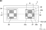
- FIG. 1 is a schematic plan view showing a semiconductor device according to the first embodiment of the present invention.
- FIG. 2 is a schematic cross-sectional view showing a portion corresponding to the line segments A1-A2 in FIG.
- the length direction, the width direction, and the thickness direction of the semiconductor device are defined by the arrows L, W, and T, respectively, as shown in FIGS. 1, 2, and 2. ..
- the length direction L, the width direction W, and the thickness direction T are orthogonal to each other.
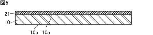
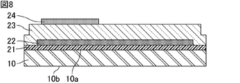
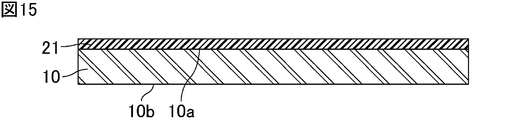
- the semiconductor device 1 includes a semiconductor substrate 10 and a circuit layer 20.
- the semiconductor substrate 10 has a first main surface 10a and a second main surface 10b facing the thickness direction T.
- the first main surface 10a and the second main surface 10b face each other in the thickness direction T.
- Examples of the constituent material of the semiconductor substrate 10 include semiconductors such as Si (silicon) and SiGe (silicon germanium).
- Electrical resistivity of the semiconductor substrate 10 is preferably 10 -5 Omega ⁇ cm or more, or less 10 5 ⁇ ⁇ cm.
- the dimension of the semiconductor substrate 10 in the length direction L is preferably 200 ⁇ m or more and 600 ⁇ m or less.
- the dimensions of the semiconductor substrate 10 in the width direction W are preferably 100 ⁇ m or more and 300 ⁇ m or less.
- the dimensions of the semiconductor substrate 10 in the thickness direction T are preferably 100 ⁇ m or more and 250 ⁇ m or less.
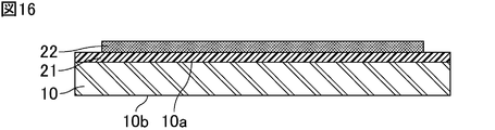
- the circuit layer 20 is provided on the first main surface 10a of the semiconductor substrate 10.
- the circuit layer 20 includes an insulating layer 21, a first electrode layer 22, a dielectric layer 23, a second electrode layer 24, a protective layer 26, a first external electrode 27, and a second external electrode 28. Have.
- the dimension of the circuit layer 20 in the thickness direction T is preferably 30 ⁇ m or more and 70 ⁇ m or less.
- the dimension of the circuit layer 20 in the thickness direction T is located on the outermost surface of the first external electrode 27 and the second external electrode 28 on the side opposite to the semiconductor substrate 10 from the surface of the insulating layer 21 on the semiconductor substrate 10 side. It is determined by the dimension to the surface to be used.
- the insulating layer 21 is provided on the entire surface of the first main surface 10a of the semiconductor substrate 10.
- the insulating layer 21 may be provided on a part of the first main surface 10a of the semiconductor substrate 10, but needs to be provided in a region overlapping the first electrode layer 22.
- the insulating layer is formed on the first main surface 10a of the semiconductor substrate 10 by oxidizing the first main surface 10a of the semiconductor substrate 10 by a thermal oxidation method or forming a film by a sputtering method or a chemical vapor deposition (CVD) method. After forming once on the entire surface and then removing a part of the insulating layer by an etching method, the insulating layer 21 can be provided on a part of the first main surface 10a of the semiconductor substrate 10.
- Examples of the constituent materials of the insulating layer 21 include SiO, SiO 2 (both silicon oxide), SiN (silicon nitride), Al 2 O 3 (aluminum oxide), HfO 2 (hafnium oxide), and Ta 2 O 5 (oxidation). Tantalum), ZrO 2 (zirconium oxide) and the like.
- the insulating layer 21 may have a single-layer structure or a multi-layer structure including a plurality of layers made of the above-mentioned materials.
- the dimension of the insulating layer 21 in the thickness direction T is preferably 0.5 ⁇ m or more and 3 ⁇ m or less.
- the first electrode layer 22 is provided on the surface of the circuit layer 20 on the semiconductor substrate 10 side, here, on the surface of the insulating layer 21 opposite to the semiconductor substrate 10.
- the first electrode layer 22 may be provided up to a position separated from the end portion of the semiconductor substrate 10. More specifically, the end portion of the first electrode layer 22 may be located inside the end portion of the semiconductor substrate 10. In a plan view as shown in FIG. 1, the distance between the end portion of the first electrode layer 22 and the end portion of the semiconductor substrate 10 is preferably 5 ⁇ m or more and 30 ⁇ m or less.
- the constituent materials of the first electrode layer 22 include Al (aluminum), Si (silicon), Cu (copper), Ag (silver), Au (gold), Ni (nickel), Cr (chromium), and Ti ( Metals such as titanium) can be mentioned.
- the constituent material of the first electrode layer 22 may be an alloy containing at least one of the above-mentioned metals, and specific examples thereof include AlSi (aluminum-silicon alloy), AlCu (aluminum-copper alloy), and AlSiCu (aluminum). -Silicon-Copper alloy) and the like.
- the first electrode layer 22 may have a single layer structure or a multilayer structure including a plurality of conductor layers made of the above-mentioned materials.
- the dimension T1 of the first electrode layer 22 in the thickness direction T is preferably 0.3 ⁇ m or more and 10 ⁇ m or less, and more preferably 0.5 ⁇ m or more and 5 ⁇ m or less.
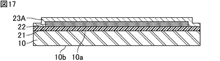
- the dielectric layer 23 is provided between the first electrode layer 22 and the second electrode layer 24 in a cross-sectional view as shown in FIG. Further, the dielectric layer 23 is provided so as to cover the first electrode layer 22 at a portion other than the opening 23h, and the end portion of the dielectric layer 23 is the end portion of the semiconductor substrate 10 from the end portion of the first electrode layer 22. It is also provided on the surface of the insulating layer 21 up to.
- the constituent materials of the dielectric layer 23 include SiN (silicon nitride), SiO 2 (silicon oxide), SiON (silicon oxynitride), Al 2 O 3 (aluminum oxide), HfO 2 (hafnium oxide), and Ta 2. O 5 (tantalum oxide) and the like can be mentioned. Above all, the dielectric layer 23 preferably contains SiN (silicon nitride).
- the second electrode layer 24 is provided so as to face the first electrode layer 22. More specifically, the second electrode layer 24 is provided on the surface of the dielectric layer 23 opposite to the semiconductor substrate 10, and faces the first electrode layer 22 with the dielectric layer 23 interposed therebetween.
- constituent materials of the second electrode layer 24 include Al (aluminum), Si (silicon), Cu (copper), Ag (silver), Au (gold), Ni (nickel), Cr (chromium), and Ti ( Metals such as titanium) can be mentioned.
- the constituent material of the second electrode layer 24 may be an alloy containing at least one of the above-mentioned metals, and specific examples thereof include AlSi (aluminum-silicon alloy), AlCu (aluminum-copper alloy), and AlSiCu (aluminum). -Silicon-Copper alloy) and the like.
- the second electrode layer 24 may have a single layer structure or a multilayer structure including a plurality of conductor layers made of the above-mentioned materials.
- the dimension T2 of the second electrode layer 24 in the thickness direction T is preferably 0.3 ⁇ m or more and 10 ⁇ m or less, and more preferably 0.5 ⁇ m or more and 5 ⁇ m or less.
- a capacitor element is composed of a first electrode layer 22, a dielectric layer 23, and a second electrode layer 24. More specifically, the capacitance of the capacitor element is formed in the region where the first electrode layer 22, the dielectric layer 23, and the second electrode layer 24 overlap.
- the capacitor element may be a stack type as shown in FIG. 2 or a trench type.
- the protective layer 26 is provided on the surface of the dielectric layer 23 opposite to the semiconductor substrate 10, and extends so as to cover the end portion of the second electrode layer 24. Further, the protective layer 26 is provided with an opening at a position overlapping the opening 23h of the dielectric layer 23 (an opening overlapping the first electrode layer 22) and a position overlapping the opening 23h of the second electrode layer 24. By providing the protective layer 26, the capacitor element, particularly the dielectric layer 23, is sufficiently protected from moisture.
- Examples of the constituent material of the protective layer 26 include resins such as polyimide resin, polybenzoxazole resin, benzocyclobutene resin, and resin in solder resist.
- the dimension of the protective layer 26 in the thickness direction T is preferably 1 ⁇ m or more and 20 ⁇ m or less.
- the first external electrode 27 is electrically connected to the first electrode layer 22. More specifically, the openings provided in the dielectric layer 23 and the protective layer 26 are extended by communicating with each other along the thickness direction T, and the first external electrode 27 is the first electrode through the openings. It is electrically connected to layer 22. Further, the first external electrode 27 is not electrically connected to the second electrode layer 24 because it is separated from the second electrode layer 24 on the surfaces along the length direction L and the width direction W. Further, the first external electrode 27 is drawn out at a position separated from the second external electrode 28 on the surface of the circuit layer 20 opposite to the semiconductor substrate 10.
- the first external electrode 27 may have a single-layer structure or a multi-layer structure.
- the constituent materials thereof include, for example, Au (gold), Ag (silver), Cu (copper), Pd (palladium), Ni (nickel), and Ti (titanium). , Al (aluminum), alloys containing at least one of these metals, and the like.
- the first external electrode 27 may have a seed layer, a first plating layer, and a second plating layer in this order from the semiconductor substrate 10 side.
- Examples of the seed layer of the first external electrode 27 include a laminate (Ti / Cu) of a conductor layer made of Ti (titanium) and a conductor layer made of Cu (copper).
- Examples of the constituent material of the first plating layer of the first external electrode 27 include Ni (nickel) and the like.
- Examples of the constituent material of the second plating layer of the first external electrode 27 include Au (gold), Sn (tin) and the like.
- the second external electrode 28 is electrically connected to the second electrode layer 24. More specifically, the opening provided in the protective layer 26 extends along the thickness direction T, and the second external electrode 28 is electrically connected to the second electrode layer 24 via the opening. There is. Further, the second external electrode 28 is not electrically connected to the first electrode layer 22 by being separated from the first electrode layer 22 on the surfaces along the length direction L and the thickness direction T. Further, the second external electrode 28 is drawn out at a position separated from the first external electrode 27 on the surface of the circuit layer 20 opposite to the semiconductor substrate 10.
- the second external electrode 28 may have a single-layer structure or a multi-layer structure.
- the constituent materials thereof include, for example, Au (gold), Ag (silver), Cu (copper), Pd (palladium), Ni (nickel), and Ti (titanium). , Al (aluminum), alloys containing at least one of these metals, and the like.
- the second external electrode 28 may have a seed layer, a first plating layer, and a second plating layer in this order from the semiconductor substrate 10 side.
- Examples of the seed layer of the second external electrode 28 include a laminate (Ti / Cu) of a conductor layer made of Ti (titanium) and a conductor layer made of Cu (copper).
- Examples of the constituent material of the first plating layer of the second external electrode 28 include Ni (nickel) and the like.
- Examples of the constituent material of the second plating layer of the second external electrode 28 include Au (gold), Sn (tin) and the like.
- the constituent material of the first external electrode 27 and the constituent material of the second external electrode 28 may be the same as each other or may be different from each other.
- the opening 23h provided in the dielectric layer 23 is a first region in which the dielectric layer 23 is not provided.
- the edge portion (inner peripheral edge portion) surrounding the opening 23h of the dielectric layer 23 is annular in the plan view as shown in FIG. 1, and a part thereof is annular in the cross-sectional view as shown in FIG. It is shown as an end portion 23a and an end portion 23b on the opening 23h side of the above.
- the end portion 23a of the dielectric layer 23 on the opening 23h side is in contact with the first electrode layer 22 on the surface on the first electrode layer 22 side.
- the dimension Ta of the end portion 23a in the thickness direction T is smaller than the dimension Tc of the inter-electrode portion 23c located between the first electrode layer 22 and the second electrode layer 24 in the thickness direction T.
- the end portion 23a of the dielectric layer 23 has a portion existing on the first external electrode 27 side from the position indicated by the dotted line F1 in the cross-sectional view as shown in FIG. 2, that is, the dimension Ta in the thickness direction T. Refers to a part smaller than the dimension Tc.
- the end portion 23a of the dielectric layer 23 overlaps the first external electrode 27 in the opening 23h.
- the dimension Ta of the end 23a of the dielectric layer 23 in the thickness direction T is smaller than the dimension Tc of the inter-electrode portion 23c in the thickness direction T, the internal stress of the end 23a, which is likely to start peeling, is reduced. Therefore, in the vicinity of the opening 23h of the dielectric layer 23, peeling between the end portion 23a of the dielectric layer 23 and the first electrode layer 22 is prevented. Similarly, peeling between the end portion 23a of the dielectric layer 23 and the first external electrode 27 is also prevented. As a result, the characteristics of the capacitor element are not deteriorated, so that the reliability is prevented from being lowered.
- the dimension in the thickness direction T on the opening 23h side is smaller than the dimension in the thickness direction T on the side opposite to the opening 23h.
- the internal stress of the tip of the end 23a on the opening 23h side which is more likely to start peeling, is reduced. Therefore, peeling of the dielectric layer 23 in the vicinity of the opening 23h is more reliably prevented.
- an end portion 23b facing the end portion 23a in the cross-sectional view as shown in FIG. 2 exists.
- the end portion 23b of the dielectric layer 23 on the opening 23h side is in contact with the first electrode layer 22 on the surface on the first electrode layer 22 side.
- the dimension Tb of the end portion 23b in the thickness direction T is smaller than the dimension Tc of the inter-electrode portion 23c in the thickness direction T.
- the end portion 23b of the dielectric layer 23 has a portion existing on the first external electrode 27 side from the dotted line F2 in the cross-sectional view as shown in FIG. 2, that is, the dimension Tb in the thickness direction T is larger than the dimension Tc. Refers to the small part.
- the end portion 23b of the dielectric layer 23 overlaps the first external electrode 27 in the opening 23h.
- the dimension Tb in the thickness direction T of the end portion 23b of the dielectric layer 23 is smaller than the dimension Tc in the thickness direction T of the inter-electrode portion 23c, the internal stress of the end portion 23b that is likely to start peeling is reduced. Therefore, in the vicinity of the opening 23h of the dielectric layer 23, peeling between the end portion 23b of the dielectric layer 23 and the first electrode layer 22 is prevented. Similarly, peeling between the end portion 23b of the dielectric layer 23 and the first external electrode 27 is also prevented. As a result, the characteristics of the capacitor element are not deteriorated, so that the reliability is prevented from being lowered.
- the dimension in the thickness direction T on the opening 23h side is smaller than the dimension in the thickness direction T on the side opposite to the opening 23h.
- the internal stress at the tip of the end 23b on the opening 23h side which is more likely to start peeling, is reduced. Therefore, peeling of the dielectric layer 23 in the vicinity of the opening 23h is more reliably prevented.
- both the dimension Ta in the thickness direction T of the end portion 23a and the dimension Tb in the thickness direction T of the end portion 23b are both in the thickness direction T of the inter-electrode portion 23c.
- one of the dimension Ta in the thickness direction T of the end portion 23a and the dimension Tb in the thickness direction T of the end portion 23b may be smaller than the dimension Tc in the thickness direction T of the inter-electrode portion 23c. ..
- both the dimension Ta in the thickness direction T of the end portion 23a and the dimension Tb in the thickness direction T of the end portion 23b are both in the thickness direction of the inter-electrode portion 23c. It is preferably smaller than the dimension Tc at T.
- the dimension Ta of the end portion 23a in the thickness direction T becomes continuously smaller toward the center of the opening 23h. More specifically, the end portion 23a of the dielectric layer 23 is in contact with the first electrode layer 22, and the cross-sectional shape of the end portion 23a of the dielectric layer 23 is a tapered shape, here, a so-called linear tapered shape. ..
- the inclination angle ⁇ a of the tapered shape is preferably 30 ° or more and 60 ° or less.
- the angle of inclination ⁇ a of the tapered shape at the end 23a of the dielectric layer 23 refers to the angle formed by the side in contact with the first electrode layer 22 and the side in contact with the first external electrode 27 in a cross-sectional view as shown in FIG. ..
- La is preferably 50% or more of the dimension Tc in the thickness direction T of the inter-electrode portion 23c. Further, the distance La is preferably 200% or less of the dimension Tc in the thickness direction T of the inter-electrode portion 23c.
- La is preferably 1% or more of the diameter D of the opening 23h. Further, the distance La is preferably 50% or less of the diameter D of the opening 23h.
- the diameter D of the opening 23h of the dielectric layer 23 refers to the maximum diameter of the opening 23h, as shown in FIGS. 1 and 2.
- the cross-sectional shape of the end portion 23a of the dielectric layer 23 is other than the linear taper shape as shown in FIG. 2 as a form in which the dimension Ta in the thickness direction T is continuously reduced toward the center of the opening 23h.
- it may have the following tapered shape.
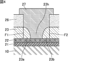
- FIG. 3 is a schematic cross-sectional view showing another form example of the end portion of the dielectric layer in FIG. In FIG. 3, the vicinity of the opening of the dielectric layer is shown. As shown in FIG. 3, the cross-sectional shape of the end portion 23a of the dielectric layer 23 is a so-called exponential taper shape.
- FIG. 4 is a schematic cross-sectional view showing still another morphological example of the end portion of the dielectric layer in FIG. In FIG. 4, the vicinity of the opening of the dielectric layer is shown. As shown in FIG. 4, the cross-sectional shape of the end portion 23a of the dielectric layer 23 is a so-called parabolic taper shape.
- the dimension Tb of the end portion 23b in the thickness direction T becomes continuously smaller toward the center of the opening 23h. More specifically, the end portion 23b of the dielectric layer 23 is in contact with the first electrode layer 22, and the cross-sectional shape of the end portion 23b of the dielectric layer 23 is a tapered shape, here, a so-called linear tapered shape. ..
- the inclination angle ⁇ b of the tapered shape is preferably 30 ° or more and 60 ° or less.
- the tapered inclination angle ⁇ b at the end 23b of the dielectric layer 23 refers to the angle formed by the side in contact with the first electrode layer 22 and the side in contact with the first external electrode 27 in a cross-sectional view as shown in FIG. ..
- Lb is preferably 50% or more of the dimension Tc in the thickness direction T of the inter-electrode portion 23c. Further, the distance Lb is preferably 200% or less of the dimension Tc in the thickness direction T of the inter-electrode portion 23c.
- Lb is preferably 1% or more of the diameter D of the opening 23h. Further, the distance Lb is preferably 50% or less of the diameter D of the opening 23h.
- the cross-sectional shape of the end portion 23b of the dielectric layer 23 is other than the linear taper shape as shown in FIG. 2 as a form in which the dimension Tb in the thickness direction T is continuously reduced toward the center of the opening 23h.
- an exponential taper shape as shown in FIG. 3 and a parabolic taper shape as shown in FIG. 4 may be used.
- the sum (La + Lb) of the distance La and the distance Lb in the dielectric layer 23 is smaller than the diameter D of the opening 23h.
- the dimension Td in the thickness direction T of the outer peripheral edge portion 23d located on the outer peripheral edge of the circuit layer 20 is preferably smaller than the dimension Tc in the thickness direction T of the inter-electrode portion 23c.
- peeling may occur between the outer peripheral edge portion 23d of the dielectric layer 23 and the insulating layer 21.
- the dimension Td of the outer peripheral edge portion 23d of the dielectric layer 23 in the thickness direction T is small, the internal stress of the outer peripheral edge portion 23d of the dielectric layer 23 is reduced. Therefore, on the outer peripheral edge of the circuit layer 20, peeling between the outer peripheral edge portion 23d of the dielectric layer 23 and the insulating layer 21 is prevented.
- the dimension Tc of the dielectric layer 23 between the electrodes 23c in the thickness direction T may be 1 ⁇ m or more.
- the dimension of the dielectric layer in the thickness direction in the thickness direction is increased in order to adjust the capacitance of the capacitor element, for example, when it is 0.1 ⁇ m or more, the internal stress of the dielectric layer increases, so that the dielectric material is used. Peeling is likely to occur near the opening of the layer. Further, according to the study by the present inventors, it was found that when the dimension of the dielectric layer between the electrodes in the thickness direction is 1 ⁇ m or more, peeling occurs remarkably in the vicinity of the opening of the dielectric layer.
- the semiconductor device 1 since the internal stress of the end 23a and the end 23b of the dielectric layer 23 becomes small, the dimension of the inter-electrode portion 23c of the dielectric layer 23 in the thickness direction T.
- Tc is large, specifically, even if the dimension Tc of the dielectric layer 23 between the electrodes 23c in the thickness direction T is 1 ⁇ m or more, peeling of the dielectric layer 23 in the vicinity of the opening 23h is prevented.
- the dimension Tc of the dielectric layer 23 between the electrodes 23c in the thickness direction T is equal to or greater than the dimension T1 in the thickness direction T of the first electrode layer 22 or the dimension T2 in the thickness direction T of the second electrode layer 24. You may. According to the studies by the present inventors, conventionally, the dimension of the dielectric layer between the electrodes in the thickness direction is equivalent to the dimension in the thickness direction of the first electrode layer or the dimension in the thickness direction of the second electrode layer. From the above, it was found that the internal stress of the dielectric layer is remarkably increased, so that the dielectric layer is remarkably peeled off in the vicinity of the opening.
- the semiconductor device 1 since the internal stress of the end 23a and the end 23b of the dielectric layer 23 becomes small, the dimension of the inter-electrode portion 23c of the dielectric layer 23 in the thickness direction T. Even if the Tc is equal to or greater than the dimension T1 in the thickness direction T of the first electrode layer 22 or the dimension T2 in the thickness direction T of the second electrode layer 24, peeling of the dielectric layer 23 in the vicinity of the opening 23h is prevented. Will be done.
- the plane as shown in FIG. 1 A scanning electron microscope (SEM) is used for a cross section as shown in FIG. 2 obtained by visually confirming a position where the diameter D of the opening 23h of the dielectric layer 23 is maximized and then cutting at that position. ), It can be measured by analysis with a transmission electron microscope (TEM) or the like.
- the dimension Tc of the dielectric layer 23 between the electrodes 23c in the thickness direction T is determined as the average value of the measured values at five points in the cross section as shown in FIG.
- a moisture-resistant protective layer may be provided between the dielectric layer 23 and the protective layer 26, and between the second electrode layer 24 and the protective layer 26. More specifically, a moisture-resistant protective layer extending from the surface of the dielectric layer 23 opposite to the semiconductor substrate 10 so as to cover the end portion of the second electrode layer 24 may be provided. In this case, the moisture-resistant protective layer is provided at a position overlapping the openings of the dielectric layer 23 and the protective layer 26 (openings overlapping the first electrode layer 22) and at the openings of the protective layer 26 (openings overlapping the second electrode layer 24). An opening will be provided at each of the overlapping positions. By providing the moisture-resistant protective layer, the moisture resistance of the capacitor element, particularly the dielectric layer 23, is enhanced.
- Examples of the constituent material of the moisture-resistant protective layer include SiN (silicon nitride) and SiO 2 (silicon oxide).
- the protective layer 26 extends from the surface of the protective layer 26 on the side opposite to the semiconductor substrate 10 so as to cover the end of the first external electrode 27 and the end of the second external electrode 28.
- An additional protective layer may be provided separately from the above.
- the additional protective layer is provided with openings at each of a position where a part of the first external electrode 27 is exposed and a position where a part of the second external electrode 28 is exposed. Since the additional protective layer is provided, when the semiconductor device 1 is mounted on the wiring board, solder is applied to each of the first external electrode 27 and the second external electrode 28 through the openings provided in the additional protective layer. It can be reliably contacted.
- constituent material of the additional protective layer examples include resins such as polyimide resin, polybenzoxazole resin, benzocyclobutene resin, and resin in solder resist.
- FIG. 2 The semiconductor device 1 shown in FIG. 2 is manufactured by, for example, the following method.
- FIG. 6, FIG. 7, FIG. 8, FIG. 9, FIG. 10, and FIG. 11 are schematic cross-sectional views for explaining an example of the method for manufacturing the semiconductor device according to the first embodiment of the present invention.
- the insulating layer 21 is formed on the first main surface 10a of the semiconductor substrate 10 by, for example, a thermal oxidation method, a sputtering method, or a chemical vapor deposition method.
- a conductor layer made of a constituent material of the first electrode layer 22 is formed on the surface of the insulating layer 21 opposite to the semiconductor substrate 10 by, for example, a sputtering method. After that, the patterning of the conductor layer is performed by combining the photolithography method and the etching method to form the first electrode layer 22 as shown in FIG. More specifically, the first electrode layer 22 is formed up to a position separated from the end portion of the semiconductor substrate 10.
- the dielectric layer 23 is formed so as to cover the first electrode layer 22 by, for example, a sputtering method or a chemical vapor deposition method.
- a conductor layer made of a constituent material of the second electrode layer 24 is formed on the surface of the dielectric layer 23 opposite to the semiconductor substrate 10 by, for example, a sputtering method. After that, the patterning of the conductor layer is performed, for example, by combining a photolithography method and an etching method to form the second electrode layer 24 as shown in FIG. More specifically, the second electrode layer 24 is formed so as to face the first electrode layer 22 with the dielectric layer 23 interposed therebetween.
- ⁇ Formation of openings in the dielectric layer> As shown in FIG. 9, by performing anisotropic etching on the dielectric layer 23, for example, an opening 23h having a tapered cross-sectional shape and exposing a part of the first electrode layer 22 is provided. Form. Such anisotropic etching is realized, for example, by performing plasma etching of the dielectric layer 23 while forming a deposit of a reactant of the depositary gas on the side wall.
- the end portion 23a of the dielectric layer 23 is in contact with the first electrode layer 22 on the surface on the side of the first electrode layer 22, and its cross-sectional shape is tapered. Ta decreases continuously toward the center of the opening 23h. Therefore, the dimension Ta of the end portion 23a of the dielectric layer 23 in the thickness direction is smaller than the dimension Tc of the inter-electrode portion 23c in the thickness direction.
- the dimension Tb in the thickness direction of the end portion 23b is formed. Continues to decrease toward the center of the opening 23h. Therefore, the dimension Tb of the end portion 23b of the dielectric layer 23 in the thickness direction is smaller than the dimension Tc of the inter-electrode portion 23c in the thickness direction.
- a layer made of the constituent material of the protective layer 26 is formed on the surface of the structure shown in FIG. 9 opposite to the semiconductor substrate 10 by, for example, a spin coating method. After that, for patterning of this layer, for example, when the constituent material of the protective layer 26 is photosensitive, only the photolithography method is used, and when the constituent material of the protective layer 26 is non-photosensitive, the photolithography method and By performing the etching method in combination, the protective layer 26 as shown in FIG. 10 is formed. More specifically, an opening is provided at each of a position overlapping the opening 23h of the dielectric layer 23 for exposing a part of the first electrode layer 22 and a position for exposing a part of the second electrode layer 24. The protective layer 26 is formed so as to be used.
- the first external electrode 27 and the second external electrode 28 are formed by, for example, combining a plating process and a photolithography method. More specifically, the first external electrode 27 is formed so as to be electrically connected to the first electrode layer 22 through the openings provided in the dielectric layer 23 and the protective layer 26, respectively. Further, the second external electrode 28 is formed so as to be electrically connected to the second electrode layer 24 through the opening provided in the protective layer 26.
- the circuit layer 20 as shown in FIG. 11 is formed on the first main surface 10a of the semiconductor substrate 10.
- the first external electrode 27 is drawn out at a position separated from the second external electrode 28 on the surface of the circuit layer 20 opposite to the semiconductor substrate 10.
- the second external electrode 28 is drawn out at a position separated from the first external electrode 27 on the surface of the circuit layer 20 opposite to the semiconductor substrate 10.
- the semiconductor device 1 shown in FIG. 2 (FIG. 11) is manufactured.
- the semiconductor substrate 10 is cut by dicing or the like.
- a plurality of semiconductor devices 1 may be manufactured at the same time by individualizing them.
- the capacitance device of the present invention includes a substrate having a first main surface and a second main surface facing each other in the thickness direction, and a circuit layer provided on the first main surface of the substrate, and the circuit layer is on the substrate side.
- the first external electrode is electrically connected to the first electrode layer via the first region in which the dielectric layer is not provided, and the end portion of the dielectric layer on the first region side is the first.
- the surface of the dielectric layer that is in contact with the first electrode layer is in contact with the first electrode layer, and the dimension of the end portion in the thickness direction is the thickness direction of the inter-electrode portion located between the first electrode layer and the second electrode layer. It is characterized by being smaller than the dimensions.
- the capacitance device according to the first embodiment of the present invention is the same as the semiconductor device according to the first embodiment of the present invention, except that the type of substrate on which the circuit layer is provided on the first main surface is not limited to the semiconductor substrate.
- the substrate for example, in addition to the semiconductor substrate such as Si (silicon) and SiGe (silicon germanium), a ceramic substrate such as alumina, a glass ceramic substrate, a glass substrate, sapphire, and MgO Examples thereof include single crystal substrates such as (magnesium oxide) and SrTIO (strontium titanate).
- the dimension of the end portion in the thickness direction may be gradually reduced toward the center of the opening.
- the semiconductor device of the second embodiment of the present invention is the same as the semiconductor device of the first embodiment of the present invention except for the structure of the dielectric layer.
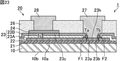
- FIG. 12 is a schematic cross-sectional view showing the semiconductor device according to the second embodiment of the present invention.
- the end portion 23a of the dielectric layer 23 on the opening 23h side is in contact with the first electrode layer 22 on the surface on the first electrode layer 22 side.
- the dimension Ta of the end portion 23a in the thickness direction T is smaller than the dimension Tc of the inter-electrode portion 23c in the thickness direction T.
- the end portion 23b of the dielectric layer 23 on the opening 23h side is in contact with the first electrode layer 22 on the surface on the first electrode layer 22 side.
- the dimension Tb of the end portion 23b in the thickness direction T is smaller than the dimension Tc of the inter-electrode portion 23c in the thickness direction T.
- both the dimension Ta in the thickness direction T of the end portion 23a and the dimension Tb in the thickness direction T of the end portion 23b are both in the thickness direction T of the inter-electrode portion 23c.
- one of the dimension Ta in the thickness direction T of the end portion 23a and the dimension Tb in the thickness direction T of the end portion 23b may be smaller than the dimension Tc in the thickness direction T of the inter-electrode portion 23c. ..
- both the dimension Ta in the thickness direction T of the end portion 23a and the dimension Tb in the thickness direction T of the end portion 23b are both in the thickness direction of the inter-electrode portion 23c. It is preferably smaller than the dimension Tc at T.
- the dimension Ta of the end portion 23a in the thickness direction T gradually decreases toward the center of the opening 23h. More specifically, the end portion 23a of the dielectric layer 23 is in contact with the first electrode layer 22, and the cross-sectional shape of the end portion 23a of the dielectric layer 23 is a stepped shape. In the cross-sectional view as shown in FIG. 12, there is a step between the surface 23as of the end portion 23a of the dielectric layer 23 and the surface of the first electrode layer 22, and the number of steps is one.
- the surface 23as of the end portion 23a of the dielectric layer 23 is preferably a flat surface, but the dielectric layer constituting the end portion 23a, here, the second dielectric described later. It may be a surface having a height difference within ⁇ 10% of the dimension of the body layer 23B in the thickness direction T.
- the dielectric layer 23 has a multilayer structure at least in the inter-electrode portion 23c, and the number of layers constituting the end portion 23a in the dielectric layer 23 may be smaller than the number of layers constituting the inter-electrode portion 23c.
- the dielectric layer 23 has a two-layer structure in which the first dielectric layer 23A and the second dielectric layer 23B are laminated at the inter-electrode portion 23c. Further, in the dielectric layer 23, the number of layers forming the end portion 23a is one layer of the second dielectric layer 23B, which is smaller than the number of layers forming the inter-electrode portion 23c.
- the dielectric layer 23 Since the dielectric layer 23 has such a structure, it becomes easy to realize a form in which the dimension Ta of the end portion 23a in the thickness direction T gradually decreases toward the center of the opening 23h.
- the end portion 23a may have a multilayer structure.
- the inter-electrode portion 23c may have a multi-layer structure of three or more layers.
- the dimension Tb of the end portion 23b in the thickness direction T gradually decreases toward the center of the opening 23h. More specifically, the end portion 23b of the dielectric layer 23 is in contact with the first electrode layer 22, and the cross-sectional shape of the end portion 23b of the dielectric layer 23 is a stepped shape. In the cross-sectional view as shown in FIG. 12, there is a step between the surface 23bs of the end portion 23b of the dielectric layer 23 and the surface of the first electrode layer 22, and the number of steps is one.
- the surface 23bs of the end portion 23b of the dielectric layer 23 is preferably a flat surface, but the dielectric layer constituting the end portion 23b, here, the second dielectric described later. It may be a surface having a height difference within ⁇ 10% of the dimension of the body layer 23B in the thickness direction T.
- the dielectric layer 23 has a multilayer structure at least in the inter-electrode portion 23c, and the number of layers constituting the end portion 23b in the dielectric layer 23 may be smaller than the number of layers constituting the inter-electrode portion 23c.
- the dielectric layer 23 has a two-layer structure in which the first dielectric layer 23A and the second dielectric layer 23B are laminated at the inter-electrode portion 23c. Further, in the dielectric layer 23, the number of layers forming the end portion 23b is one layer of the second dielectric layer 23B, which is smaller than the number of layers forming the inter-electrode portion 23c.
- the dielectric layer 23 Since the dielectric layer 23 has such a structure, it becomes easy to realize a form in which the dimension Tb of the end portion 23b in the thickness direction T gradually decreases toward the center of the opening 23h.
- the end portion 23b may have a multilayer structure.
- the inter-electrode portion 23c may have a multi-layer structure of three or more layers.
- the dielectric layer 23 has a multilayer structure.
- the plurality of layers included in the multilayer structure of the dielectric layer 23 may be made of the same material.
- the first dielectric layer 23A and the second dielectric layer 23B may be made of the same material.
- Such same materials include SiN (silicon nitride), SiO 2 (silicon oxide), SiON (silicon oxynitride), Al 2 O 3 (aluminum oxide), HfO 2 (hafnium oxide), and Ta 2 O 5 (Ta 2 O 5 (). It is preferably selected from the group consisting of tantalum oxide).
- a plurality of layers included in the multilayer structure of the dielectric layer 23 are made of the same material.
- FIG. By observing the cross section as shown in the above with a transmission electron microscope (TEM), the interface between the first dielectric layer 23A and the second dielectric layer 23B made of the same material can be confirmed.
- TEM transmission electron microscope
- the plurality of layers included in the multilayer structure of the dielectric layer 23 may be made of different materials.
- the first dielectric layer 23A and the second dielectric layer 23B may be made of different materials.
- Such different materials include SiN (silicon nitride), SiO 2 (silicon oxide), SiON (silicon oxynitride), Al 2 O 3 (aluminum oxide), HfO 2 (hafnium oxide), and Ta 2 O 5 (Ta 2 O 5 (). It is preferably selected from the group consisting of tantalum oxide).
- the layer on the first electrode layer 22 side of the inter-electrode portion 23c is made of SiO 2 (silicon oxide). It is preferable that the layer of the end portion 23a on the side of the first electrode layer 22 is made of SiN (silicon nitride).
- SiO 2 silicon oxide
- the layer of the end portion 23a on the side of the first electrode layer 22 is made of SiN (silicon nitride).
- the layer on the first electrode layer 22 side of the inter-electrode portion 23c, that is, the first dielectric layer 23A is composed of SiO 2 (silicon oxide) and
- the layer on the side of the first electrode layer 22 of the end portion 23a, that is, the second dielectric layer 23B is preferably made of SiN (silicon nitride).
- the layer on the first electrode layer 22 side of the inter-electrode portion 23c is SiO 2 (silicon oxide).
- the layer on the side of the first electrode layer 22 of the end portion 23b is preferably made of SiN (silicon nitride).
- the layer on the first electrode layer 22 side of the inter-electrode portion 23c, that is, the first dielectric layer 23A is composed of SiO 2 (silicon oxide) and
- the layer on the side of the first electrode layer 22 of the end portion 23b, that is, the second dielectric layer 23B is preferably made of SiN (silicon nitride).
- the multilayer structure of the dielectric layer 23 is made of the material as described above, the coefficient of thermal expansion of the portion of the dielectric layer 23 on the first electrode layer 22 side and the first electrode layer 22 tends to be close to each other. , The peeling between the dielectric layer 23 and the first electrode layer 22 is sufficiently prevented.
- the number of stages of each of the end portion 23a and the end portion 23b of the dielectric layer 23 may be one stage as shown in FIG. 12 or two or more stages.
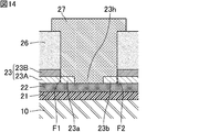
- the end portion 23a and the end portion 23b of the dielectric layer 23 may have a structure as shown in FIG. 13 or FIG.
- FIG. 13 is a schematic cross-sectional view showing another form example of the end portion of the dielectric layer in FIG. In FIG. 13, the vicinity of the opening of the dielectric layer is shown.
- the first dielectric layer 23A is formed when the second dielectric layer 23B is formed. Does not damage.
- the first dielectric layer 23A and the second dielectric layer 23B are not limited in their constituent materials, and may be composed of the same material or different materials.
- the ends 23a and 23b of the dielectric layer 23 shown in FIG. 13 are also prevented from being peeled off in the same manner as the ends 23a and 23b of the dielectric layer 23 shown in FIG.
- FIG. 14 is a schematic cross-sectional view showing still another morphological example of the end portion of the dielectric layer in FIG. In FIG. 14, the vicinity of the opening of the dielectric layer is shown.
- the first dielectric layer 23A is formed when the second dielectric layer 23B is formed. May be damaged.
- the first dielectric layer 23A and the second dielectric layer 23B have restrictions on their respective constituent materials, and need to be composed of different materials.
- the ends 23a and 23b of the dielectric layer 23 shown in FIG. 14 are also prevented from being peeled off in the same manner as the ends 23a and 23b of the dielectric layer 23 shown in FIG.
- the semiconductor device 1 shown in FIG. 12 is manufactured by, for example, the following method.
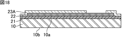
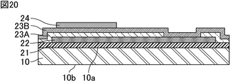
- FIG. 16, FIG. 17, FIG. 18, FIG. 19, FIG. 20, FIG. 21, FIG. 22, and FIG. 23 are cross sections for explaining an example of the method for manufacturing the semiconductor device according to the second embodiment of the present invention. It is a schematic diagram.
- the insulating layer 21 is formed on the first main surface 10a of the semiconductor substrate 10 by, for example, a thermal oxidation method, a sputtering method, or a chemical vapor deposition method.
- a conductor layer made of a constituent material of the first electrode layer 22 is formed on the surface of the insulating layer 21 opposite to the semiconductor substrate 10 by, for example, a sputtering method. After that, the patterning of the conductor layer is performed by combining the photolithography method and the etching method to form the first electrode layer 22 as shown in FIG. More specifically, the first electrode layer 22 is formed up to a position separated from the end portion of the semiconductor substrate 10.
- the first dielectric layer 23A is formed so as to cover the first electrode layer 22 by, for example, a sputtering method or a chemical vapor deposition method.
- the first dielectric layer 23A is patterned by combining, for example, a photolithography method and an etching method. As a result, as shown in FIG. 18, an opening for exposing a part of the first electrode layer 22 is formed in the first dielectric layer 23A.
- the second dielectric layer 23B is formed on the surface of the structure shown in FIG. 18 opposite to the semiconductor substrate 10 by, for example, a sputtering method or a chemical vapor deposition method.
- a conductor layer made of a constituent material of the second electrode layer 24 is formed on the surface of the second dielectric layer 23B opposite to the semiconductor substrate 10 by, for example, a sputtering method. After that, the patterning of the conductor layer is performed, for example, by combining a photolithography method and an etching method to form the second electrode layer 24 as shown in FIG. More specifically, the second electrode layer 24 is formed so as to face the first electrode layer 22 with the first dielectric layer 23A and the second dielectric layer 23B interposed therebetween.
- the second dielectric layer 23B is patterned by combining, for example, a photolithography method and an etching method. As a result, as shown in FIG. 21, an opening for exposing a part of the first electrode layer 22 within the opening of the first dielectric layer 23A is formed in the second dielectric layer 23B.
- the end portion 23a of the dielectric layer 23 is in contact with the first electrode layer 22 on the surface on the first electrode layer 22 side, and the cross-sectional shape thereof is a stepped shape.
- the dimension Ta in the thickness direction of the end portion 23a of the dielectric layer 23 is smaller than the dimension Tc in the thickness direction of the inter-electrode portion 23c.
- the end portion 23b of the dielectric layer 23 is in contact with the first electrode layer 22 on the surface on the first electrode layer 22 side, and its cross-sectional shape is a stepped shape.
- the dimension Tb of the end portion 23b of the dielectric layer 23 in the thickness direction is smaller than the dimension Tc of the inter-electrode portion 23c in the thickness direction.
- the internal stress remains toward the outside in the longitudinal direction and the other is formed so that the internal stress remains toward the inside in the longitudinal direction.
- the internal stress is easily canceled between the first dielectric layer 23A and the second dielectric layer 23B, so that the dielectric material is formed. It contributes to the prevention of peeling of the layer 23.
- a layer made of the constituent material of the protective layer 26 is formed on the surface of the structure shown in FIG. 21 opposite to the semiconductor substrate 10 by, for example, a spin coating method. After that, for patterning of this layer, for example, when the constituent material of the protective layer 26 is photosensitive, only the photolithography method is used, and when the constituent material of the protective layer 26 is non-photosensitive, the photolithography method and By performing the etching method in combination, the protective layer 26 as shown in FIG. 22 is formed. More specifically, an opening is provided at each of a position overlapping the opening 23h of the dielectric layer 23 for exposing a part of the first electrode layer 22 and a position for exposing a part of the second electrode layer 24. The protective layer 26 is formed so as to be used.
- the first external electrode 27 and the second external electrode 28 are formed by, for example, combining a plating process and a photolithography method. More specifically, the first external electrode 27 is formed so as to be electrically connected to the first electrode layer 22 through the openings provided in the dielectric layer 23 and the protective layer 26, respectively. Further, the second external electrode 28 is formed so as to be electrically connected to the second electrode layer 24 through the opening provided in the protective layer 26.
- the circuit layer 20 as shown in FIG. 23 is formed on the first main surface 10a of the semiconductor substrate 10.
- the first external electrode 27 is drawn out at a position separated from the second external electrode 28 on the surface of the circuit layer 20 opposite to the semiconductor substrate 10.
- the second external electrode 28 is drawn out at a position separated from the first external electrode 27 on the surface of the circuit layer 20 opposite to the semiconductor substrate 10.
- the semiconductor device 1 shown in FIG. 12 (FIG. 23) is manufactured.
- the capacitance device of the second embodiment of the present invention is the same as the semiconductor device of the second embodiment of the present invention, except that the type of the substrate on which the circuit layer is provided on the first main surface is not limited to the semiconductor substrate.
- Examples of the substrate in the capacitance device according to the second embodiment of the present invention include the same substrate as the substrate in the capacitance device according to the first embodiment of the present invention.
- the first external electrode and the first The electrode layer was electrically connected via an opening provided in the dielectric layer, but the electrode layer is not limited to the opening of the dielectric layer, and is electrically connected through a first region in which the dielectric layer is not provided. It only needs to be connected.
- the dielectric layer 23 can form a capacitor element if it exists at least in the inter-electrode portion 23c, the dielectric layer 23 extends to the first external electrode 27 side. You don't have to.
- the end portion 23a of the dielectric layer 23 is separated from the first external electrode 27 by the protective layer 26, and may be in contact with the inter-electrode portion 23c. Further, since the dielectric layer 23 is not provided with an opening, the end portion 23b does not exist.
Landscapes
- Engineering & Computer Science (AREA)
- Power Engineering (AREA)
- Microelectronics & Electronic Packaging (AREA)
- Manufacturing & Machinery (AREA)
- Chemical & Material Sciences (AREA)
- Ceramic Engineering (AREA)
- Inorganic Chemistry (AREA)
- Semiconductor Integrated Circuits (AREA)
- Ceramic Capacitors (AREA)
- Fixed Capacitors And Capacitor Manufacturing Machines (AREA)
- Internal Circuitry In Semiconductor Integrated Circuit Devices (AREA)
Priority Applications (3)
| Application Number | Priority Date | Filing Date | Title |
|---|---|---|---|
| JP2021572745A JP7363928B2 (ja) | 2020-01-20 | 2021-01-19 | 半導体装置及び容量装置 |
| CN202180009644.5A CN114981904B (zh) | 2020-01-20 | 2021-01-19 | 半导体装置以及电容装置 |
| US17/859,128 US12424389B2 (en) | 2020-01-20 | 2022-07-07 | Semiconductor device and capacitance device |
Applications Claiming Priority (2)
| Application Number | Priority Date | Filing Date | Title |
|---|---|---|---|
| JP2020-006848 | 2020-01-20 | ||
| JP2020006848 | 2020-01-20 |
Related Child Applications (1)
| Application Number | Title | Priority Date | Filing Date |
|---|---|---|---|
| US17/859,128 Continuation US12424389B2 (en) | 2020-01-20 | 2022-07-07 | Semiconductor device and capacitance device |
Publications (1)
| Publication Number | Publication Date |
|---|---|
| WO2021149688A1 true WO2021149688A1 (ja) | 2021-07-29 |
Family
ID=76992976
Family Applications (1)
| Application Number | Title | Priority Date | Filing Date |
|---|---|---|---|
| PCT/JP2021/001714 Ceased WO2021149688A1 (ja) | 2020-01-20 | 2021-01-19 | 半導体装置及び容量装置 |
Country Status (4)
| Country | Link |
|---|---|
| US (1) | US12424389B2 (https=) |
| JP (1) | JP7363928B2 (https=) |
| CN (1) | CN114981904B (https=) |
| WO (1) | WO2021149688A1 (https=) |
Cited By (1)
| Publication number | Priority date | Publication date | Assignee | Title |
|---|---|---|---|---|
| WO2024014351A1 (ja) * | 2022-07-13 | 2024-01-18 | 株式会社村田製作所 | キャパシタ |
Families Citing this family (1)
| Publication number | Priority date | Publication date | Assignee | Title |
|---|---|---|---|---|
| CN115943470B (zh) * | 2020-06-29 | 2025-11-14 | Tdk株式会社 | 薄膜电容器及具备其的电子电路基板 |
Citations (7)
| Publication number | Priority date | Publication date | Assignee | Title |
|---|---|---|---|---|
| JPH0547586A (ja) * | 1991-08-16 | 1993-02-26 | Toshiba Corp | コンデンサ部品 |
| JP2005079513A (ja) * | 2003-09-03 | 2005-03-24 | Seiko Epson Corp | 半導体装置及びその製造方法 |
| JP2005191182A (ja) * | 2003-12-25 | 2005-07-14 | Nec Electronics Corp | 半導体装置及びその製造方法 |
| JP2008153497A (ja) * | 2006-12-19 | 2008-07-03 | Murata Mfg Co Ltd | 誘電体薄膜キャパシタの製造方法 |
| JP2016219588A (ja) * | 2015-05-20 | 2016-12-22 | イビデン株式会社 | 薄膜キャパシタ |
| US9761655B1 (en) * | 2016-06-20 | 2017-09-12 | International Business Machines Corporation | Stacked planar capacitors with scaled EOT |
| WO2019026771A1 (ja) * | 2017-07-31 | 2019-02-07 | 株式会社村田製作所 | キャパシタ |
Family Cites Families (20)
| Publication number | Priority date | Publication date | Assignee | Title |
|---|---|---|---|---|
| US6885081B2 (en) * | 2000-11-13 | 2005-04-26 | Sharp Kabushiki Kaisha | Semiconductor capacitor device having reduced voltage dependence |
| US20030011043A1 (en) * | 2001-07-14 | 2003-01-16 | Roberts Douglas R. | MIM capacitor structure and process for making the same |
| US7078785B2 (en) * | 2003-09-23 | 2006-07-18 | Freescale Semiconductor, Inc. | Semiconductor device and making thereof |
| CN101197210A (zh) * | 2006-12-05 | 2008-06-11 | 泉州市火炬电子元件厂 | 多层陶瓷电容器及其制造方法 |
| JP4930602B2 (ja) * | 2007-12-14 | 2012-05-16 | 株式会社村田製作所 | 薄膜積層キャパシタの製造方法 |
| KR101090932B1 (ko) * | 2008-12-24 | 2011-12-08 | 매그나칩 반도체 유한회사 | 캐패시터 및 그의 제조방법 |
| JP5407775B2 (ja) * | 2009-03-31 | 2014-02-05 | Tdk株式会社 | 薄膜コンデンサの製造方法及び薄膜コンデンサ |
| JP5234521B2 (ja) | 2009-08-21 | 2013-07-10 | Tdk株式会社 | 電子部品及びその製造方法 |
| CN103098199B (zh) * | 2010-09-13 | 2014-12-10 | 株式会社村田制作所 | 电介质薄膜元件、反熔丝元件及电介质薄膜元件的制造方法 |
| JP2012164714A (ja) * | 2011-02-03 | 2012-08-30 | Rohm Co Ltd | 半導体装置の製造方法および半導体装置 |
| US9257498B1 (en) * | 2014-08-04 | 2016-02-09 | Taiwan Semiconductor Manufacturing Co., Ltd. | Process to improve performance for metal-insulator-metal (MIM) capacitors |
| WO2018003445A1 (ja) * | 2016-06-28 | 2018-01-04 | 株式会社村田製作所 | キャパシタ |
| US10468187B2 (en) * | 2016-08-05 | 2019-11-05 | Samsung Electro-Mechanics Co., Ltd. | Thin-film ceramic capacitor having capacitance forming portions separated by separation slit |
| KR102748948B1 (ko) * | 2016-08-26 | 2025-01-02 | 삼성전기주식회사 | 박막 커패시터 및 그 제조방법 |
| WO2019026641A1 (ja) * | 2017-07-31 | 2019-02-07 | 株式会社村田製作所 | 薄膜コンデンサ及びその製造方法 |
| WO2019203054A1 (ja) * | 2018-04-18 | 2019-10-24 | 株式会社村田製作所 | キャパシタおよびその製造方法 |
| CN112041954B (zh) * | 2018-04-27 | 2022-08-02 | 株式会社村田制作所 | 电容器集合体 |
| US10615249B2 (en) * | 2018-07-19 | 2020-04-07 | Vanguard International Semiconductor Corporation | Capacitor structures and methods for fabricating the same |
| US11410921B2 (en) * | 2018-08-21 | 2022-08-09 | Intel Corporation | Methods to incorporate thin film capacitor sheets (TFC-S) in the build-up films |
| US11171199B2 (en) * | 2019-08-23 | 2021-11-09 | Taiwan Semiconductor Manufacturing Co., Ltd. | Metal-insulator-metal capacitors with high breakdown voltage |
-
2021
- 2021-01-19 JP JP2021572745A patent/JP7363928B2/ja active Active
- 2021-01-19 WO PCT/JP2021/001714 patent/WO2021149688A1/ja not_active Ceased
- 2021-01-19 CN CN202180009644.5A patent/CN114981904B/zh active Active
-
2022
- 2022-07-07 US US17/859,128 patent/US12424389B2/en active Active
Patent Citations (7)
| Publication number | Priority date | Publication date | Assignee | Title |
|---|---|---|---|---|
| JPH0547586A (ja) * | 1991-08-16 | 1993-02-26 | Toshiba Corp | コンデンサ部品 |
| JP2005079513A (ja) * | 2003-09-03 | 2005-03-24 | Seiko Epson Corp | 半導体装置及びその製造方法 |
| JP2005191182A (ja) * | 2003-12-25 | 2005-07-14 | Nec Electronics Corp | 半導体装置及びその製造方法 |
| JP2008153497A (ja) * | 2006-12-19 | 2008-07-03 | Murata Mfg Co Ltd | 誘電体薄膜キャパシタの製造方法 |
| JP2016219588A (ja) * | 2015-05-20 | 2016-12-22 | イビデン株式会社 | 薄膜キャパシタ |
| US9761655B1 (en) * | 2016-06-20 | 2017-09-12 | International Business Machines Corporation | Stacked planar capacitors with scaled EOT |
| WO2019026771A1 (ja) * | 2017-07-31 | 2019-02-07 | 株式会社村田製作所 | キャパシタ |
Cited By (3)
| Publication number | Priority date | Publication date | Assignee | Title |
|---|---|---|---|---|
| WO2024014351A1 (ja) * | 2022-07-13 | 2024-01-18 | 株式会社村田製作所 | キャパシタ |
| JPWO2024014351A1 (https=) * | 2022-07-13 | 2024-01-18 | ||
| JP7768388B2 (ja) | 2022-07-13 | 2025-11-12 | 株式会社村田製作所 | キャパシタ |
Also Published As
| Publication number | Publication date |
|---|---|
| JPWO2021149688A1 (https=) | 2021-07-29 |
| JP7363928B2 (ja) | 2023-10-18 |
| CN114981904B (zh) | 2024-07-05 |
| US20220336155A1 (en) | 2022-10-20 |
| CN114981904A (zh) | 2022-08-30 |
| US12424389B2 (en) | 2025-09-23 |
Similar Documents
| Publication | Publication Date | Title |
|---|---|---|
| US12288646B2 (en) | Capacitor with connection conductor contacting a surface of a substrate | |
| CN110959188B (zh) | 电容器 | |
| JP6372640B2 (ja) | キャパシタ | |
| US12424389B2 (en) | Semiconductor device and capacitance device | |
| US12464740B2 (en) | Semiconductor device and module | |
| TWI611487B (zh) | 半導體裝置及半導體裝置之製造方法 | |
| US8164160B2 (en) | Semiconductor device | |
| US20080296772A1 (en) | Semicondutor device | |
| CN109923630B (zh) | 电容器 | |
| JP7563591B2 (ja) | 半導体装置、マッチング回路及びフィルタ回路 | |
| US10813220B2 (en) | Electronic component embedded substrate | |
| US12424383B2 (en) | Semiconductor device | |
| JP2009088002A (ja) | 半導体装置及びその製造方法 | |
| JPWO2019208221A1 (ja) | キャパシタ集合体 | |
| JP2020170782A (ja) | キャパシタ | |
| US20240063252A1 (en) | Semiconductor device and module | |
| US20240071691A1 (en) | Semiconductor device | |
| US12431290B2 (en) | Semiconductor device and module | |
| US12362096B2 (en) | Chip parts | |
| CN112151494B (zh) | 一种半导体器件及其形成方法 | |
| JP2006210589A (ja) | 薄膜コンデンサ | |
| CN121264190A (zh) | 半导体装置 | |
| JP2009088001A (ja) | 半導体装置及びその製造方法 | |
| JPH05144808A (ja) | 半導体装置及びその製造方法 | |
| JP2004014853A (ja) | 薄膜コンデンサ |
Legal Events
| Date | Code | Title | Description |
|---|---|---|---|
| 121 | Ep: the epo has been informed by wipo that ep was designated in this application |
Ref document number: 21744890 Country of ref document: EP Kind code of ref document: A1 |
|
| ENP | Entry into the national phase |
Ref document number: 2021572745 Country of ref document: JP Kind code of ref document: A |
|
| NENP | Non-entry into the national phase |
Ref country code: DE |
|
| 122 | Ep: pct application non-entry in european phase |
Ref document number: 21744890 Country of ref document: EP Kind code of ref document: A1 |