WO2021059890A1 - マスクブランク、位相シフトマスク及び半導体デバイスの製造方法 - Google Patents
マスクブランク、位相シフトマスク及び半導体デバイスの製造方法 Download PDFInfo
- Publication number
- WO2021059890A1 WO2021059890A1 PCT/JP2020/033040 JP2020033040W WO2021059890A1 WO 2021059890 A1 WO2021059890 A1 WO 2021059890A1 JP 2020033040 W JP2020033040 W JP 2020033040W WO 2021059890 A1 WO2021059890 A1 WO 2021059890A1
- Authority
- WO
- WIPO (PCT)
- Prior art keywords
- phase shift
- film
- shift film
- mask
- atomic
- Prior art date
- Legal status (The legal status is an assumption and is not a legal conclusion. Google has not performed a legal analysis and makes no representation as to the accuracy of the status listed.)
- Ceased
Links
Images

Classifications
-
- G—PHYSICS
- G03—PHOTOGRAPHY; CINEMATOGRAPHY; ANALOGOUS TECHNIQUES USING WAVES OTHER THAN OPTICAL WAVES; ELECTROGRAPHY; HOLOGRAPHY
- G03F—PHOTOMECHANICAL PRODUCTION OF TEXTURED OR PATTERNED SURFACES, e.g. FOR PRINTING, FOR PROCESSING OF SEMICONDUCTOR DEVICES; MATERIALS THEREFOR; ORIGINALS THEREFOR; APPARATUS SPECIALLY ADAPTED THEREFOR
- G03F1/00—Originals for photomechanical production of textured or patterned surfaces, e.g., masks, photo-masks, reticles; Mask blanks or pellicles therefor; Containers specially adapted therefor; Preparation thereof
- G03F1/26—Phase shift masks [PSM]; PSM blanks; Preparation thereof
- G03F1/34—Phase-edge PSM, e.g. chromeless PSM; Preparation thereof
-
- G—PHYSICS
- G03—PHOTOGRAPHY; CINEMATOGRAPHY; ANALOGOUS TECHNIQUES USING WAVES OTHER THAN OPTICAL WAVES; ELECTROGRAPHY; HOLOGRAPHY
- G03F—PHOTOMECHANICAL PRODUCTION OF TEXTURED OR PATTERNED SURFACES, e.g. FOR PRINTING, FOR PROCESSING OF SEMICONDUCTOR DEVICES; MATERIALS THEREFOR; ORIGINALS THEREFOR; APPARATUS SPECIALLY ADAPTED THEREFOR
- G03F1/00—Originals for photomechanical production of textured or patterned surfaces, e.g., masks, photo-masks, reticles; Mask blanks or pellicles therefor; Containers specially adapted therefor; Preparation thereof
- G03F1/26—Phase shift masks [PSM]; PSM blanks; Preparation thereof
-
- C—CHEMISTRY; METALLURGY
- C23—COATING METALLIC MATERIAL; COATING MATERIAL WITH METALLIC MATERIAL; CHEMICAL SURFACE TREATMENT; DIFFUSION TREATMENT OF METALLIC MATERIAL; COATING BY VACUUM EVAPORATION, BY SPUTTERING, BY ION IMPLANTATION OR BY CHEMICAL VAPOUR DEPOSITION, IN GENERAL; INHIBITING CORROSION OF METALLIC MATERIAL OR INCRUSTATION IN GENERAL
- C23C—COATING METALLIC MATERIAL; COATING MATERIAL WITH METALLIC MATERIAL; SURFACE TREATMENT OF METALLIC MATERIAL BY DIFFUSION INTO THE SURFACE, BY CHEMICAL CONVERSION OR SUBSTITUTION; COATING BY VACUUM EVAPORATION, BY SPUTTERING, BY ION IMPLANTATION OR BY CHEMICAL VAPOUR DEPOSITION, IN GENERAL
- C23C14/00—Coating by vacuum evaporation, by sputtering or by ion implantation of the coating forming material
- C23C14/06—Coating by vacuum evaporation, by sputtering or by ion implantation of the coating forming material characterised by the coating material
- C23C14/10—Glass or silica
-
- G—PHYSICS
- G03—PHOTOGRAPHY; CINEMATOGRAPHY; ANALOGOUS TECHNIQUES USING WAVES OTHER THAN OPTICAL WAVES; ELECTROGRAPHY; HOLOGRAPHY
- G03F—PHOTOMECHANICAL PRODUCTION OF TEXTURED OR PATTERNED SURFACES, e.g. FOR PRINTING, FOR PROCESSING OF SEMICONDUCTOR DEVICES; MATERIALS THEREFOR; ORIGINALS THEREFOR; APPARATUS SPECIALLY ADAPTED THEREFOR
- G03F1/00—Originals for photomechanical production of textured or patterned surfaces, e.g., masks, photo-masks, reticles; Mask blanks or pellicles therefor; Containers specially adapted therefor; Preparation thereof
- G03F1/26—Phase shift masks [PSM]; PSM blanks; Preparation thereof
- G03F1/32—Attenuating PSM [att-PSM], e.g. halftone PSM or PSM having semi-transparent phase shift portion; Preparation thereof
Definitions
- the present invention relates to a mask blank for a phase shift mask, a phase shift mask, and a method for manufacturing a semiconductor device.
- a fine pattern is formed using a photolithography method.
- a number of transfer masks are usually used to form this fine pattern.
- an ArF excimer laser (wavelength 193 nm) has been increasingly applied as an exposure light source when manufacturing a semiconductor device.
- CPL mask chromeless phase shift mask
- an etching stopper film is provided on the translucent substrate, and a phase shift film containing silicon and oxygen and having a transmittance substantially equal to that of the translucent substrate is provided on the etching stopper film. It is known that it has a structure.
- a CPL mask a mask in which a digging portion and a non-digging portion are provided on a substrate transparent to exposure light and a transfer pattern is formed by the digging portion and the non-digging portion is also known.
- an etching stop layer, a phase shift layer pattern, and a light-shielding layer pattern are provided in this order on a transparent substrate, and a silicon nitride film (Si 3 N 4 film) is provided as an etching stop layer, and a phase shift layer is provided.
- An optical mask blank is disclosed in which SiO 2 films are provided in this order, and a low-reflection chromium light-shielding film in which a chromium oxide film, a metallic chromium film, and a chromium oxide film are laminated in this order as a light-shielding layer is provided.
- Patent Document 2 in a chromeless phase shift mask in which a digging portion is provided in a substrate transparent to exposure light and the phase of transmitted light is controlled, a portion adjacent to the substrate digging portion or a peripheral portion of the substrate is provided.
- the CPL mask basically has only a strong phase shift effect generated between the exposure light transmitted through the digging portion and the exposure light transmitted through the non-digging portion in the region where the digging portion is formed in a plan view. It is configured to create a transferred image. The smaller the difference between the transmittance of the dug portion and the transmittance of the non-drilled portion with respect to the exposure light, the stronger the phase shift effect. Further, in the case of the CPL mask, in order to improve the CD uniformity of the transferred image, the difference between the phase shift effects generated between the dug portion and the non-drilled portion in the plane should be reduced. Is desired. That is, it is desired that the depths of the dug portions provided in the plane be the same.
- the digging portion of the conventional CPL mask is formed by digging the translucent substrate to a predetermined depth by dry etching.
- the present invention has been made to solve the conventional problems, and it is possible to increase the transmittance of the ArF excimer laser with respect to the exposure light and suppress the film thickness required to secure a desired phase difference. It is an object of the present invention to provide a mask blank provided with a phase shift film. Further, the present invention includes a phase shift film having a transfer pattern capable of increasing the transmittance of the ArF excimer laser with respect to the exposure light and suppressing the film thickness required to secure a desired phase difference. It is intended to provide a mask. Then, the present invention provides a method for manufacturing a semiconductor device using such a phase shift mask.
- the present invention has the following configuration as a means for solving the above problems.
- the phase shift film contains silicon, oxygen and nitrogen and
- the ratio of the nitrogen content [atomic%] to the silicon content [atomic%] of the phase shift film is 0.20 or more and 0.52 or less.
- the ratio of the oxygen content [atomic%] to the silicon content [atomic%] of the phase shift film is 1.16 or more and 1.70 or less.
- the refractive index n of the phase shift film with respect to the wavelength of the exposure light of the ArF excimer laser is 1.7 or more and 2.0 or less.
- the phase shift film has a function of transmitting the exposure light with a transmittance of 70% or more, and has passed through the air for the same distance as the thickness of the phase shift film with respect to the exposure light transmitted through the phase shift film.
- (Structure 5) The mask blank according to any one of configurations 1 to 4, wherein the phase shift film has a thickness of 140 nm or less.
- phase shift mask provided with a phase shift film having a transfer pattern on the main surface of a translucent substrate.
- the phase shift film contains silicon, oxygen and nitrogen and The ratio of the nitrogen content [atomic%] to the silicon content [atomic%] of the phase shift film is 0.20 or more and 0.52 or less.
- the ratio of the oxygen content [atomic%] to the silicon content [atomic%] of the phase shift film is 1.16 or more and 1.70 or less.
- the refractive index n of the phase shift film with respect to the wavelength of the exposure light of the ArF excimer laser is 1.7 or more and 2.0 or less.
- a phase shift mask characterized in that the extinction coefficient k of the phase shift film with respect to the wavelength of the exposure light is 0.05 or less.
- phase shift mask according to the configuration 7 or 8, wherein the silicon content of the phase shift film is 30 atomic% or more.
- the phase shift film has a function of transmitting the exposure light with a transmittance of 70% or more, and has passed through the air for the same distance as the thickness of the phase shift film with respect to the exposure light transmitted through the phase shift film.
- phase shift mask according to any one of configurations 7 to 10, wherein the phase shift film has a thickness of 140 nm or less.
- Structure 12 The phase shift mask according to any one of configurations 7 to 11, wherein a light-shielding film having a pattern including a light-shielding band is provided on the phase-shift film.
- Structure 13 A method for manufacturing a semiconductor device, which comprises a step of exposing and transferring a transfer pattern to a resist film on a semiconductor substrate using the phase shift mask according to the configuration 12.
- the mask blank of the present invention having the above configuration is a mask blank having a phase shift film on the main surface of a translucent substrate, and the phase shift film contains silicon, oxygen and nitrogen, and the phase shift film is contained.
- the ratio of the nitrogen content [atomic%] to the silicon content [atomic%] of the shift film is 0.20 or more and 0.52 or less, and oxygen to the silicon content [atomic%] of the phase shift film.
- the ratio of the content [atomic%] of is 1.16 or more and 1.70 or less, and the refractive index n with respect to the wavelength of the exposure light of the ArF excima laser of the phase shift film is 1.7 or more and 2.0 or less.
- the phase shift film has an extinction coefficient k with respect to the wavelength of the exposure light of 0.05 or less.
- phase shift mask provided with a phase shift film having a transfer pattern capable of increasing the transmittance of the ArF excimer laser with respect to the exposure light and suppressing the film thickness required to secure a desired phase difference can be manufactured. can do. Further, in the manufacture of a semiconductor device using this phase shift mask, it becomes possible to transfer a pattern to a resist film or the like on the semiconductor device with good accuracy.
- the phase shift film is desired to have a high transmittance (for example, 70% or more) with respect to ArF exposure light in order to generate a strong phase shift effect. ..
- a high transmittance for example, 70% or more
- SiO 2 of the same material system as that of the translucent substrate is suitable as the material of the phase shift film.
- the phase shift film formed of SiO 2 has a small refractive index n with respect to ArF exposure light. In order to cause the phase shift effect on the phase shift film, it is necessary to significantly increase the film thickness.
- the phase shift film composed of silicon and oxygen further contains a metal element.
- the phase shift film composed of silicon and oxygen also contains nitrogen (that is, the phase shift film is formed of a SiON-based material containing silicon, oxygen and nitrogen as main components) to contain a metal element.
- the refractive index n of the phase shift film can be increased.
- the phase shift film of the SiON-based material has a trade-off that the film thickness required to generate a strong phase shift effect decreases as the nitrogen content increases, but the transmittance decreases. There is a relationship. Therefore, when the phase shift film is formed of a SiON-based material, the nitrogen content is such that a high transmittance for ArF exposure light can be ensured while the film thickness required to generate a strong phase shift effect can be reduced. And finding a range of oxygen content is important.
- the phase shift film preferably has an amorphous structure or a microcrystal structure, it is generally formed by a sputtering method.
- a sputtering method By adjusting the pressure and sputtering voltage in the film formation chamber when the phase shift film is formed by reactive sputtering, it is possible to make the internal structure of the phase shift film somewhat sparse (a state with many gaps). ..
- the transmittance for the exposure light can be increased to some extent. By utilizing this, it seems that the decrease in ArF transmittance due to increasing the nitrogen content of the SiON-based material film can be suppressed at first glance.
- such a SiON-based material film has low physical resistance to the pattern after forming a fine pattern by dry etching, and also has low chemical resistance. Such a SiON-based material film is not suitable for a phase shift film.
- the present inventors have found a suitable phase shift film as an alternative to the digging portion of the CPL mask. That is, the phase shift film is formed of a material containing silicon, nitrogen and oxygen. Then, the ratio of the nitrogen content [atomic%] to the silicon content [atomic%] of the phase shift film is 0.20 or more and 0.52 or less, and the ratio to the oxygen content [atomic%]. The ratio of nitrogen content [atomic%] shall be 1.16 or more and 1.70 or less. Further, the refractive index n of the phase shift film with respect to the ArF exposure light is set to 1.7 or more and 2.0 or less, and the extinction coefficient k with respect to the ArF exposure light is set to 0.05 or less. With such a configuration, it is possible to generate a strong phase shift effect with a relatively thin film thickness while forming a phase shift film having a dense internal structure and having a high transmittance for ArF exposure light.
- the mask blank according to the embodiment of the present invention is a CPL (Chromeless Phase Lithography) mask, that is, a mask blank used for manufacturing a chromeless phase shift mask.
- the CPL mask is a type in which a light-shielding film is basically not provided in the transfer pattern forming region except for a large pattern region, and the transfer pattern is formed by a buried portion and a non-digged portion of a translucent substrate. It is a phase shift mask of.
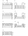
- FIG. 1 shows a schematic configuration of an embodiment of a mask blank. The mask blank 100 shown in FIG.
- the mask blank 100 has a configuration in which a phase shift film 2, a light shielding film 3, and a hard mask film 4 are laminated in this order on one main surface of the translucent substrate 1.
- the mask blank 100 may have a configuration in which the hard mask film 4 is not provided, if necessary. Further, the mask blank 100 may have a structure in which a resist film is laminated on the hard mask film 4 as needed. The details of the main components of the mask blank 100 will be described below.
- the translucent substrate 1 is made of a material having good transparency to the exposure light used in the exposure process in lithography.
- synthetic quartz glass, aluminosilicate glass, soda-lime glass, low thermal expansion glass (SiO 2- TiO 2 glass, etc.), and various other glass substrates can be used.
- the substrate using synthetic quartz glass has high transparency to ArF excimer laser light (wavelength: about 193 nm), it can be suitably used as the translucent substrate 1 of the mask blank 100.
- the exposure step in lithography referred to here is an exposure step in lithography using a phase shift mask produced by using this mask blank 100, and the exposure light is ArF excimer laser light unless otherwise specified.
- the refractive index of the material forming the translucent substrate 1 in the exposure light is preferably 1.5 or more and 1.6 or less, more preferably 1.52 or more and 1.59 or less, and 1.54 or more and 1 It is more preferably .58 or less.
- the phase shift film 2 preferably has a function of transmitting exposure light with a transmittance of 70% or more. This is because a sufficient phase shift effect is generated between the exposure light transmitted through the inside of the phase shift film 2 and the exposure light transmitted through the air. It is more preferable that the phase shift film 2 has a function of transmitting exposure light with a transmittance of 75% or more.
- the transmittance of the phase shift film 2 with respect to the exposure light is preferably 93% or less, and more preferably 90% or less. This is to limit the film thickness of the phase shift film 2 to an appropriate range in which optical performance can be ensured.
- the phase shift film 2 is between the exposure light transmitted through the phase shift film 2 and the exposure light passing through the air by the same distance as the thickness of the phase shift film 2. It is preferable that the light is adjusted so as to have a function of causing a phase difference of 150 degrees or more and 210 degrees or less.
- the phase difference in the phase shift film 2 is more preferably 155 degrees or more, and further preferably 160 degrees or more.
- the phase difference in the phase shift film 2 is more preferably 200 degrees or less, and further preferably 190 degrees or less.
- the refractive index n (hereinafter, simply referred to as the refractive index n) with respect to the wavelength of the exposure light is 1.7 or more. It is preferably 1.75 or more, and more preferably 1.75 or more.
- the refractive index n of the phase shift film 2 is preferably 2.0 or less, and more preferably 1.98 or less.
- the extinction coefficient k (hereinafter, simply referred to as the extinction coefficient k) of the phase shift film 2 with respect to the wavelength of the exposure light is preferably 0.05 or less, and more preferably 0.04 or less.
- the extinction coefficient k of the phase shift film 2 is preferably 0.005 or more, and more preferably 0.007 or more.
- the refractive index n and the extinction coefficient k of the phase shift film 2 are numerical values derived by regarding the entire phase shift film 2 as one optically uniform layer.
- the refractive index n and the extinction coefficient k of the thin film including the phase shift film 2 are not determined only by the composition of the thin film.
- the film density and crystal state of the thin film are also factors that influence the refractive index n and the extinction coefficient k. Therefore, various conditions for forming a thin film by reactive sputtering are adjusted so that the thin film has a desired refractive index n and extinction coefficient k.
- a mixed gas of a noble gas and a reactive gas oxygen gas, nitrogen gas, etc.
- the film thickness of the phase shift film 2 is preferably 140 nm or less in order to reduce the occurrence of pattern collapse.
- the film thickness of the phase shift film 2 is preferably 95 nm or more, and more preferably 100 nm or more, in order to secure the function of producing a desired phase difference.
- the phase shift film 2 preferably contains silicon, nitrogen and oxygen.
- the total content of silicon, nitrogen and oxygen in the phase shift film 2 is preferably 97 atomic% or more, more preferably 98 atomic% or more, and further preferably 99 atomic% or more.
- the content of the metal element is preferably less than 1 atomic%, and more preferably not more than the lower limit of detection. This is because when the phase shift film 2 contains a metal element, the extinction coefficient k increases.
- the phase shift film 2 is preferably formed of a material composed of silicon, oxygen and nitrogen, or is formed of a material composed of one or more elements selected from metalloid elements and non-metal elements, silicon, oxygen and nitrogen. You may. This is because if the contents of the metalloid element and the non-metal element are to some extent, the influence on the optical characteristics of the phase shift film 2 is minor. On the other hand, the phase shift film 2 may contain any metalloid element. Among these metalloid elements, when one or more elements selected from boron, germanium, antimony and tellurium are contained, the conductivity of silicon used as a target when the phase shift film 2 is formed by a sputtering method can be enhanced. It is preferable because it can be expected.
- the phase shift film 2 can be patterned by dry etching using a fluorine-based gas, and has sufficient etching selectivity with respect to the light-shielding film 3 described later.
- the oxygen content of the phase shift membrane 2 is preferably 42 atomic% or more, and more preferably 43 atomic% or more, from the viewpoint of increasing the transmittance.
- the oxygen content of the phase shift film 2 is preferably 60 atomic% or less, and more preferably 58 atomic% or less, from the viewpoint of suppressing a decrease in the refractive index n.
- the nitrogen content of the phase shift film 2 is preferably 6 atomic% or more, and more preferably 7 atomic% or more, from the viewpoint of increasing the refractive index n.
- the nitrogen content of the phase shift film 2 is preferably 22 atomic% or less, and more preferably 20 atomic% or less, from the viewpoint of suppressing an increase in the extinction coefficient k.
- the silicon content of the phase shift film 2 is preferably 30 atomic% or more, and more preferably 33 atomic% or more, from the viewpoint of enhancing physical resistance and chemical resistance.
- the silicon content of the phase shift film 2 is preferably 40 atomic% or less, and more preferably 38 atomic% or less, from the viewpoint of increasing the transmittance.
- the N / Si ratio in the phase shift film 2 is preferably 0.20 or more, and more preferably 0.22 or more, from the viewpoint of increasing the refractive index n.
- the N / Si ratio is preferably 0.52 or less, and more preferably 0.51 or less, from the viewpoint of suppressing an increase in the extinction coefficient k.
- the O / Si ratio in the phase shift film 2 is preferably 1.16 or more, and more preferably 1.17 or more, from the viewpoint of increasing the transmittance.
- the O / Si ratio is preferably 1.70 or less, and more preferably 1.69 or less, from the viewpoint of suppressing a decrease in the refractive index n.
- the ratio of the nitrogen content [atomic%] to the oxygen content [atomic%] of the phase shift film 2 (hereinafter referred to as N / O ratio) is 0.12 or more from the viewpoint of increasing the refractive index n. It is preferably 0.13 or more, and more preferably 0.13 or more. On the other hand, this N / O ratio is preferably 0.45 or less, and more preferably 0.44 or less, from the viewpoint of suppressing an increase in the extinction coefficient k.
- the phase shift film 2 is preferably a single-layer film having a uniform composition, but is not necessarily limited to this, and may be formed of a plurality of layers and has a composition in the thickness direction. It may have an inclined configuration.
- the mask blank 100 includes a light-shielding film 3 on the phase shift film 2.
- the outer peripheral region of the region where the transfer pattern is formed is the exposure light transmitted through the outer peripheral region when exposure-transferred to a resist film on a semiconductor wafer using an exposure apparatus. It is required to secure an optical density (OD) equal to or higher than a predetermined value so that the resist film is not affected.
- the outer peripheral region of the phase shift mask preferably has an OD of 2.8 or more, and more preferably 3.0 or more.
- the phase shift film 2 has a function of transmitting exposure light with a transmittance of 70% or more, and it is difficult to secure a predetermined value of optical density only with the phase shift film 2. Therefore, at the stage of manufacturing the mask blank 100, it is necessary to laminate the light-shielding film 3 on the phase-shift film 2 in order to secure the insufficient optical density.
- the light-shielding film 3 in the region where the phase shift effect is used (basically the transfer pattern forming region) is removed during the manufacturing of the phase shift mask 200 (see FIG. 2). Then, the phase shift mask 200 in which the optical density of a predetermined value is secured in the outer peripheral region can be manufactured.
- the light-shielding film 3 can be applied to both a single-layer structure and a laminated structure having two or more layers. Further, even if each layer of the light-shielding film 3 having a single-layer structure and the light-shielding film 3 having a laminated structure of two or more layers has substantially the same composition in the thickness direction of the film or the layer, the composition is formed in the thickness direction of the layer. It may have an inclined configuration.
- the mask blank 100 in the embodiment shown in FIG. 1 has a configuration in which a light-shielding film 3 is laminated on the phase shift film 2 without interposing another film.
- the light-shielding film 3 in this case is preferably formed of a material containing chromium.
- the material containing chromium that forms the light-shielding film 3 include a material containing chromium metal and one or more elements selected from oxygen, nitrogen, carbon, boron, and fluorine in chromium.
- the material for forming the light-shielding film 3 is one or more elements selected from oxygen, nitrogen, carbon, boron and fluorine in chromium.
- a material containing is preferable.
- the chromium-containing material forming the light-shielding film 3 may contain one or more elements of molybdenum, indium and tin. By containing one or more elements of molybdenum, indium and tin, the etching rate for a mixed gas of chlorine-based gas and oxygen gas can be made faster.
- the mask blank 100 of the present invention is not limited to the one shown in FIG. 1, and is configured such that another film (etching mask / stopper film) is interposed between the phase shift film 2 and the light shielding film 3. You may. In this case, it is preferable that the etching mask / stopper film is formed of the chromium-containing material and the light-shielding film 3 is formed of the silicon-containing material.
- the silicon-containing material forming the light-shielding film 3 may contain a transition metal or may contain a metal element other than the transition metal.
- the pattern formed on the light-shielding film 3 is basically a light-shielding band pattern in the outer peripheral region, and the integrated irradiation amount of ArF exposure light is smaller than that in the transfer pattern region, and a fine pattern is arranged in this outer peripheral region. This is because it is rare, and even if the ArF light resistance is low, a substantial problem is unlikely to occur. Further, when the transition metal is contained in the light-shielding film 3, the light-shielding performance is greatly improved as compared with the case where the light-shielding film 3 is not contained, and the thickness of the light-shielding film 3 can be reduced.
- transition metal contained in the light-shielding film 3 examples include molybdenum (Mo), tantalum (Ta), tungsten (W), titanium (Ti), chromium (Cr), hafnium (Hf), nickel (Ni), and vanadium (V). , Zirconium (Zr), ruthenium (Ru), rhodium (Rh), niobium (Nb), palladium (Pd) and the like, or an alloy of these metals.
- the light-shielding film 3 may have a structure in which a layer made of a material containing chromium and a layer made of a material containing a transition metal and silicon are laminated in this order from the phase shift film 2 side.
- the specific matters of the material containing chromium and the material containing transition metal and silicon in this case are the same as in the case of the light-shielding film 3 described above.
- the hard mask film 4 is provided in contact with the surface of the light-shielding film 3.
- the hard mask film 4 is a film formed of a material having etching resistance against the etching gas used when etching the light-shielding film 3.
- the hard mask film 4 only needs to have a film thickness sufficient to function as an etching mask until the dry etching for forming a pattern on the light shielding film 3 is completed, and basically has optical characteristics. Not restricted by. Therefore, the thickness of the hard mask film 4 can be made significantly thinner than the thickness of the light-shielding film 3.
- the hard mask film 4 is preferably made of a material containing silicon. Since the hard mask film 4 in this case tends to have low adhesion to the resist film of the organic material, the surface of the hard mask film 4 is subjected to HMDS (Hexamethyldisilazane) treatment to improve the adhesion of the surface. Is preferable.
- the hard mask film 4 in this case is more preferably formed of SiO 2 , SiN, SiON, or the like.
- the material of the hard mask film 4 when the light-shielding film 3 is made of a material containing chromium
- a material containing tantalum can also be applied.
- the material containing tantalum in this case include, in addition to tantalum metal, a material in which tantalum contains one or more elements selected from nitrogen, oxygen, boron and carbon.
- Ta, TaN, TaO, TaON, TaBN, TaBO, TaBON, TaCN, TaCO, TaCON, TaBCN, TaBOCN and the like can be mentioned.
- the hard mask film 4 is preferably formed of the above-mentioned material containing chromium.
- the resist film of the organic material is formed with a film thickness of 100 nm or less in contact with the surface of the hard mask film 4.
- SRAF Sub-Resolution Assist Feature
- the transfer pattern phase shift pattern
- the cross-sectional aspect ratio of the resist pattern can be as low as 1: 2.5, it is possible to prevent the resist pattern from collapsing or detaching during development, rinsing, or the like of the resist film. It is more preferable that the resist film has a film thickness of 80 nm or less.
- the resist film of the organic material is formed with a film thickness of 100 nm or less in contact with the surface of the hard mask film 4.
- SRAF Sub-Resolution Assist Feature
- the film thickness of the resist film can be suppressed by providing the hard mask film 4 as described above, whereby the cross-sectional aspect ratio of the resist pattern composed of the resist film is set to 1: 2.5. Can be lowered.
- the resist film has a film thickness of 80 nm or less.
- the resist film is preferably a resist for electron beam drawing exposure, and more preferably a chemically amplified resist.
- the mask blank 100 may be provided with an etching stopper film between the translucent substrate 1 and the phase shift film 2.
- This etching stopper film is required to have sufficient etching selectivity with the phase shift film 2 with respect to dry etching when patterning the phase shift film 2. Further, the etching stopper film is also required to have a high transmittance for exposure light.
- the etching stopper film is preferably formed of a material containing one or more elements selected from aluminum and hafnium and oxygen.
- examples of the material of the etching stopper film include a material containing aluminum, silicon, and oxygen, and a material containing aluminum, hafnium, and oxygen.
- the etching stopper film is preferably formed of a material containing aluminum, hafnium, and oxygen.
- the etching stopper film can increase the transmittance for exposure light and increase the dry etching resistance to fluorine-based gas
- the ratio of the hafnium content to the total content of hafnium and aluminum by atomic% (hereinafter, Hf / [ Hf + Al] ratio may be expressed as 0.86 or less, more preferably 0.80 or less, and further preferably 0.75 or less.
- the etching stopper film preferably has an Hf / [Hf + Al] ratio of 0.40 or more.
- the etching stopper film has an Hf / [Hf + Al] ratio of 0.60. The above is more preferable.
- the etching stopper film preferably has a content of metals other than aluminum and hafnium of 2 atomic% or less, more preferably 1 atomic% or less, and is equal to or less than the lower limit of detection when composition analysis is performed by X-ray photoelectron spectroscopy. Is more preferable. This is because if the etching stopper film contains a metal other than aluminum and hafnium, it causes a decrease in the transmittance for exposure light. Further, the etching stopper film preferably has a total content of elements other than aluminum, hafnium and oxygen of 5 atomic% or less, and more preferably 3 atomic% or less.
- the etching stopper film may be formed of a material composed of hafnium, aluminum and oxygen.
- Materials composed of hafnium, aluminum, and oxygen include these constituent elements and other elements (helium (He), neon (Ne), argon) that are inevitably contained in the etching stopper film when forming a film by the sputtering method.
- a material containing only noble gases such as (Ar), krypton (Kr) and xenon (Xe), hydrogen (H), carbon (C), etc.).
- the etching stopper film preferably has an amorphous structure. More specifically, the etching stopper film preferably has an amorphous structure containing a bond of hafnium and oxygen and a bond of aluminum and oxygen. The surface roughness of the etching stopper film can be made good, and the transmittance with respect to the exposure light can be increased.
- the etching stopper film is preferable as it has a higher transmittance with respect to the exposure light.
- the transmittance with respect to the exposure light is also required. It is difficult to make the transmittance the same as that of the translucent substrate 1 (that is, when the transmittance of the translucent substrate 1 (synthetic quartz glass) with respect to the exposure light is 100%, the transmittance of the etching stopper film is 100. It will be less than%.).
- the transmittance of the translucent substrate 1 with respect to the exposure light is 100%, the transmittance of the etching stopper film is preferably 85% or more, and more preferably 90% or more.
- the etching stopper film preferably has an oxygen content of 60 atomic% or more, more preferably 61.5 atomic% or more, and further preferably 62 atomic% or more. This is because it is required that a large amount of oxygen is contained in the etching stopper film in order to make the transmittance with respect to the exposure light equal to or higher than the above value.
- the etching stopper film preferably has an oxygen content of 66 atomic% or less.
- the etching stopper film preferably has a thickness of 2 nm or more. Considering the influence of dry etching with a fluorine-based gas and the influence of chemical cleaning performed from the mask blank to the manufacture of the transfer mask, the thickness of the etching stopper film is more preferably 3 nm or more.
- the etching stopper film uses a material with high transmittance for exposure light, but the transmittance decreases as the thickness increases. Further, the etching stopper film has a higher refractive index than the material forming the translucent substrate 1, and the thicker the etching stopper film, the more the mask pattern (Bias correction, OPC, etc.) actually formed on the phase shift film 2. The influence on the design of the pattern to which SRAF or the like is added becomes large. Considering these points, the etching stopper film is preferably 10 nm or less, preferably 8 nm or less, and more preferably 6 nm or less.
- the etching stopper film preferably has a refractive index of 2.90 or less with respect to exposure light, and more preferably 2.86 or less. This is to reduce the influence on the design of the mask pattern actually formed on the phase shift film 2. Since the etching stopper film is formed of a material containing hafnium and aluminum, it cannot have the same refractive index n as that of the translucent substrate 1.
- the etching stopper film preferably has a refractive index of 2.10 or more, and more preferably 2.20 or more.
- the etching stopper film preferably has an extinction coefficient with respect to exposure light of 0.30 or less, and more preferably 0.29 or less. This is because the transmittance of the etching stopper film with respect to the exposure light is increased.
- the etching stopper film preferably has an extinction coefficient k of 0.06 or more.
- the etching stopper film has a high uniformity of composition in the thickness direction (the difference in the content of each constituent element in the thickness direction is within a fluctuation range of 5 atomic% or less).
- the etching stopper film may have a film structure whose composition is inclined in the thickness direction.
- the composition inclination is such that the Hf / [Hf + Al] ratio on the translucent substrate 1 side of the etching stopper film is lower than the Hf / [Hf + Al] ratio on the phase shift film 2 side. This is because the etching stopper film is preferably desired to have higher chemical resistance on the phase shift film 2 side, while it is desired to have higher transmittance for exposure light on the translucent substrate 1 side.
- the etching stopper film may be formed of a material made of aluminum, silicon and oxygen.
- the content of the metal other than aluminum in this etching stopper film is preferably 2 atomic% or less, more preferably 1 atomic% or less, and is equal to or less than the lower limit of detection when the composition is analyzed by X-ray photoelectron spectroscopy. Is more preferable.
- the etching stopper film preferably has a total content of elements other than silicon, aluminum and oxygen of 5 atomic% or less, and more preferably 3 atomic% or less.
- the etching stopper film is preferably formed of a material made of silicon, aluminum and oxygen.
- the materials composed of silicon, aluminum, and oxygen are elements that are inevitably contained in the etching stopper film (helium (He), neon (Ne), argon) when the film is formed by the sputtering method.
- a material containing only rare gases such as (Ar), krypton (Kr) and xenon (Xe), hydrogen (H), carbon (C), etc.).
- This etching stopper film preferably has an oxygen content of 60 atomic% or more.
- the etching stopper film has a ratio of the content [atomic%] of silicon (Si) to the total content [atomic%] of silicon (Si) and aluminum (Al) (hereinafter referred to as "Si / [Si + Al] ratio"). Is preferably 4/5 or less.
- the Si / [Si + Al] ratio in this etching stopper film is more preferably 3/4 or less, and further preferably 2/3 or less.
- the etching stopper film preferably has a Si / [Si + Al] ratio of silicon (Si) and aluminum (Al) of 1/5 or more.
- the mask blank 100 having the above configuration is manufactured by the following procedure. First, the translucent substrate 1 is prepared. In this translucent substrate 1, the end face and the main surface are polished to a predetermined surface roughness (for example, the root mean square roughness Rq is 0.2 nm or less in the inner region of a quadrangle having a side of 1 ⁇ m), and then the predetermined surface roughness is determined. It has been washed and dried.
- a predetermined surface roughness for example, the root mean square roughness Rq is 0.2 nm or less in the inner region of a quadrangle having a side of 1 ⁇ m
- the phase shift film 2 is formed on the translucent substrate 1 by a sputtering method. After the phase shift film 2 is formed, an annealing treatment at a predetermined heating temperature is appropriately performed. Next, the above-mentioned light-shielding film 3 is formed on the phase-shift film 2 by a sputtering method. Then, the above-mentioned hard mask film 4 is formed on the light-shielding film 3 by a sputtering method.
- a sputtering target and a sputtering gas containing the materials constituting each of the above films in a predetermined composition ratio are used, and if necessary, a mixed gas of the above-mentioned noble gas and the reactive gas is used.
- a film is formed using it as a sputtering gas.
- the etching stopper film described above is formed on the mask blank 100, two targets, a mixed target of hafnium and oxygen and a mixed target of aluminum and oxygen, are placed in the film forming chamber before the phase shift film 2 is formed. It is preferable that at least one of the above is arranged and an etching stopper film is formed on the translucent substrate 1 by reactive sputtering.
- FIG. 2 shows a phase shift mask 200 according to an embodiment of the present invention manufactured from the mask blank 100 of the above embodiment and a manufacturing process thereof.
- a phase shift pattern 2a which is a transfer pattern, is formed on the phase shift film 2 of the mask blank 100, and a pattern including a light shielding band is formed on the light shielding film 3.
- the light-shielding pattern 3b having the light-shielding pattern 3b is formed.
- the method for manufacturing the phase shift mask 200 uses the mask blank 100, and includes a step of forming a transfer pattern on the light-shielding film 3 by dry etching and a light-shielding film 3 having the transfer pattern.
- the method for manufacturing the phase shift mask 200 of the present invention will be described according to the manufacturing process shown in FIG.
- phase shift mask 200 using the mask blank 100 in which the hard mask film 4 is laminated on the light-shielding film 3 will be described. Further, a case where a material containing chromium is applied to the light-shielding film 3 and a material containing silicon is applied to the hard mask film 4 will be described.
- a resist film is formed by a spin coating method in contact with the hard mask film 4 of the mask blank 100.
- the first pattern which is a transfer pattern (phase shift pattern) to be formed on the phase shift film 2
- the first resist pattern 5a is formed (see FIG. 2A).
- dry etching was performed using a fluorine-based gas to form the first pattern (hard mask pattern 4a) on the hard mask film 4 (see FIG. 2B). ..
- dry etching is performed using a mixed gas of chlorine-based gas and oxygen gas using the hard mask pattern 4a as a mask, and the first pattern (light-shielding pattern 3a) is formed on the light-shielding film 3. (See FIG. 2 (c)). Subsequently, dry etching was performed using a fluorine-based gas using the light-shielding pattern 3a as a mask to form a first pattern (phase shift pattern 2a) on the phase shift film 2 and remove the hard mask pattern 4a (FIG. 6). 2 (d)).
- a resist film was formed on the mask blank 100 by a spin coating method.
- a second pattern which is a pattern to be formed on the light-shielding film 3 (light-shielding pattern)
- a second resist pattern 6b was formed (see FIG. 2E).
- dry etching was performed using a mixed gas of chlorine-based gas and oxygen gas to form a second pattern (light-shielding pattern 3b) on the light-shielding film 3 (FIG. 2 (FIG. 2). f) See).
- the second resist pattern 6b was removed, and a predetermined process such as cleaning was performed to obtain a phase shift mask 200 (see FIG. 2 (g)).
- the chlorine-based gas used in the dry etching is not particularly limited as long as it contains Cl.
- Cl 2 , NaCl 2 , CHCl 3 , CH 2 Cl 2 , CCl 4 , BCl 3, and the like can be mentioned.
- the fluorine-based gas used in the dry etching is not particularly limited as long as it contains F.
- CHF 3 , CF 4 , C 2 F 6 , C 4 F 8 , SF 6, and the like can be mentioned.
- the fluorine-based gas containing no C has a relatively low etching rate with respect to the glass substrate, damage to the glass substrate can be further reduced.
- the phase shift mask 200 manufactured by the manufacturing method shown in FIG. 2 is a phase shift mask provided with a phase shift film 2 (phase shift pattern 2a) having a transfer pattern on a translucent substrate 1.
- phase shift mask 200 By manufacturing the phase shift mask 200 in this way, the phase shift mask 200 provided with the phase shift film 2 capable of enhancing the phase shift effect on the exposure light of the ArF excimer laser and suppressing the film thickness can be obtained. Obtainable.
- a phase shift mask can also be manufactured by the manufacturing method shown in FIG. 2 using a mask blank provided with an etching stopper film. In this case, the etching stopper film remains without being removed from the phase shift mask.
- the method for manufacturing a semiconductor device of the present invention is characterized by including a step of exposing and transferring a transfer pattern to a resist film on a semiconductor substrate by using the phase shift mask 200.
- the phase shift mask 200 is set on the mask stage of the exposure apparatus using the ArF excimer laser as the exposure light, and the resist film on the semiconductor device is set.
- the transfer pattern is exposed to transfer, a fine transfer pattern can be transferred to the resist film on the semiconductor device. Therefore, when the pattern of the resist film is used as a mask and the lower layer film is dry-etched to form a circuit pattern, a high-precision circuit pattern without wiring short circuit or disconnection can be formed.
- a translucent substrate 1 made of synthetic quartz glass having a main surface size of about 152 mm ⁇ about 152 mm and a thickness of about 6.35 mm was prepared.
- the end face and the main surface of the translucent substrate 1 are polished to a predetermined surface roughness (Rq of 0.2 nm or less), and then subjected to a predetermined cleaning treatment and a drying treatment.
- Rq surface roughness
- each optical characteristic of the translucent substrate 1 was measured using a spectroscopic ellipsometer (M-2000D manufactured by JA Woollam)
- the refractive index in light having a wavelength of 193 nm was 1.556 and the extinction coefficient was 0. It was 000.
- the translucent substrate 1 is installed in the single-wafer sputtering apparatus, and the reaction using a Crypton (Kr) gas, an oxygen (O 2 ) gas, and a nitrogen (N 2 ) gas as the sputtering gas using a Si target.
- a phase shift film 2 made of silicon, oxygen, and nitrogen was formed on the translucent substrate 1 with a thickness of 136.4 nm so as to obtain a desired phase difference.
- phase shift amount measuring device MPM193 manufactured by Lasertec
- the transmittance was 92.0% and the phase difference was 179.9 degrees. It was (deg).
- each optical characteristic of the phase shift film 2 was measured using a spectroscopic ellipsometer (M-2000D manufactured by JA Woollam)
- the refractive index n in light having a wavelength of 193 nm was 1.709, and the extinction coefficient k. was 0.005.
- a phase shift film was formed on another translucent substrate under the same film forming conditions.
- phase shift film was analyzed by X-ray photoelectron spectroscopy (XPS analysis).
- the N / O ratio was 0.120
- the O / Si ratio was 1.696
- the N / Si ratio was 0.203.
- the film density was calculated for this phase shift film 2 using a measuring device (GXR-300 manufactured by Rigaku Co., Ltd.) using the X-ray reflectivity method (XRR), it was found that the film was sufficiently dense. It could be confirmed.
- the translucent substrate 1 is installed in the single-wafer sputtering apparatus, and the reactivity is carried out in a mixed gas atmosphere of argon (Ar), carbon dioxide (CO 2 ) and helium (He) using a chromium (Cr) target.
- a light-shielding film 3 (CrOC film Cr: 71 atomic%, O: 15 atomic%, C: 14 atomic%) composed of chromium, oxygen and carbon is formed in contact with the surface of the phase shift film 2 at a thickness of 59 nm. Formed.
- the translucent substrate 1 on which the light-shielding film (CrOC film) 3 was formed was heat-treated.
- a spectrophotometer Cary 4000 manufactured by Azilent Technology Co., Ltd.
- a translucent substrate 1 in which a phase shift film 2 and a light-shielding film 3 are laminated is installed in a single-wafer sputtering apparatus, and an argon (Ar) gas is sputtered using a silicon dioxide (SiO 2) target.
- a hard mask film 4 made of silicon and oxygen was formed on the light-shielding film 3 by reactive sputtering to a thickness of 12 nm. Further, a predetermined cleaning treatment was performed to produce the mask blank 100 of Example 1.
- the halftone type phase shift mask 200 of Example 1 was manufactured by the following procedure. First, the surface of the hard mask film 4 was subjected to HMDS treatment. Subsequently, a resist film made of a chemically amplified resist for electron beam writing was formed with a film thickness of 80 nm in contact with the surface of the hard mask film 4 by a spin coating method. Next, a first pattern, which is a phase shift pattern to be formed on the phase shift film 2, is electron-beam-drawn on the resist film, subjected to a predetermined development process and a cleaning process, and a resist having the first pattern is performed. A pattern 5a was formed (see FIG. 2A).
- the resist pattern 5a was removed.
- dry etching is performed using a mixed gas of chlorine gas (Cl 2 ) and oxygen gas (O 2 ) to form a first pattern (light-shielding pattern 3a) on the light-shielding film 3. (See FIG. 2 (c)).
- etching is performed using a fluorine-based gas (CF 4 + He) to form a first pattern (phase shift pattern 2a) on the phase shift film 2, and at the same time, a hard mask pattern. 4a was removed (see FIG. 2D).
- CF 4 + He fluorine-based gas
- a resist film made of a chemically amplified resist for electron beam writing was formed on the light-shielding pattern 3a by a spin coating method with a film thickness of 150 nm.
- a second pattern which is a pattern to be formed on the light-shielding film (a pattern including a light-shielding band pattern), is exposed and drawn on the resist film, and further subjected to a predetermined process such as development processing to have a light-shielding pattern.
- a resist pattern 6b was formed (see FIG. 2E).
- Example 2 [Manufacturing of mask blank]
- the mask blank 100 of Example 2 was manufactured in the same procedure as in Example 1 except for the phase shift film 2.
- the phase shift film 2 of the second embodiment has different film forming conditions from the phase shift film 2 of the first embodiment. Specifically, a translucent substrate 1 is installed in a single-wafer sputtering apparatus, a Si target is used, and the gas flow rates of oxygen gas and nitrogen gas are changed to sputter krypton gas, oxygen gas, and nitrogen gas. Reactive sputtering was performed. As a result, a phase shift film 2 made of silicon, oxygen, and nitrogen was formed on the translucent substrate 1 with a thickness of 128.7 nm so as to obtain a desired phase difference.
- phase shift amount measuring device MPM193 manufactured by Lasertec
- the transmittance was 89.5% and the phase difference was 179.7 degrees. It was (deg).
- M-2000D manufactured by JA Woollam the refractive index n in light having a wavelength of 193 nm was 1.750 and the extinction coefficient k. was 0.009.
- a phase shift film was formed on another translucent substrate under the same film forming conditions. Further, the phase shift film was analyzed by X-ray photoelectron spectroscopy (XPS analysis).
- the N / O ratio was 0.155
- the O / Si ratio was 1.636
- the N / Si ratio was 0.254.
- the film density was calculated for this phase shift film 2 using a measuring device (GXR-300 manufactured by Rigaku Co., Ltd.) using the X-ray reflectivity method (XRR), it was found that the film was sufficiently dense. It could be confirmed.
- phase shift mask 200 of Example 2 was manufactured by the same procedure as in Example 1. Simulation of a transfer image when the phase shift mask 200 of Example 2 is exposed and transferred to a resist film on a semiconductor device with exposure light having a wavelength of 193 nm using AIMS193 (manufactured by Carl Zeiss) in the same manner as in Example 1. was done. When the exposure transfer image of this simulation was verified, there were no short circuits or disconnections in the wiring, and the design specifications were fully satisfied. From this result, even if the phase shift mask 200 of the second embodiment is set on the mask stage of the exposure apparatus and exposed to the resist film on the semiconductor device, the circuit pattern finally formed on the semiconductor device is high. It can be said that it can be formed with accuracy.
- Example 3 [Manufacturing of mask blank]
- the mask blank 100 of Example 3 was manufactured in the same procedure as in Example 1 except for the phase shift film 2.
- the phase shift film 2 of the third embodiment has different film forming conditions from the phase shift film 2 of the first embodiment. Specifically, a translucent substrate 1 is installed in a single-wafer sputtering apparatus, a Si target is used, and the gas flow rates of oxygen gas and nitrogen gas are changed to sputter krypton gas, oxygen gas, and nitrogen gas. Reactive sputtering was performed. As a result, a phase shift film 2 made of silicon, oxygen, and nitrogen was formed on the translucent substrate 1 with a thickness of 108.7 nm so as to obtain a desired phase difference.
- phase shift amount measuring device MPM193 manufactured by Lasertec
- the transmittance was 80.9% and the phase difference was 181.3 degrees. It was (deg).
- each optical characteristic of the phase shift film 2 was measured using a spectroscopic ellipsometer (M-2000D manufactured by JA Woollam)
- the refractive index n in light having a wavelength of 193 nm was 1.890
- the extinction coefficient k. was 0.026.
- a phase shift film was formed on another translucent substrate under the same film forming conditions. Further, the phase shift film was analyzed by X-ray photoelectron spectroscopy (XPS analysis).
- the N / O ratio was 0.300
- the O / Si ratio was 1.373
- the N / Si ratio was 0.412.
- the film density was calculated for this phase shift film 2 using a measuring device (GXR-300 manufactured by Rigaku Co., Ltd.) using the X-ray reflectivity method (XRR), it was found that the film was sufficiently dense. It could be confirmed.
- phase shift mask 200 of Example 3 was manufactured by the same procedure as in Example 1. Simulation of a transfer image when the phase shift mask 200 of Example 3 is exposed and transferred to a resist film on a semiconductor device with exposure light having a wavelength of 193 nm using AIMS193 (manufactured by Carl Zeiss) in the same manner as in Example 1. was done. When the exposure transfer image of this simulation was verified, there were no short circuits or disconnections in the wiring, and the design specifications were fully satisfied. From this result, even if the phase shift mask 200 of Example 3 is set on the mask stage of the exposure apparatus and exposed and transferred to the resist film on the semiconductor device, the circuit pattern finally formed on the semiconductor device is high. It can be said that it can be formed with accuracy.
- Example 4 [Manufacturing of mask blank]
- the mask blank 100 of Example 4 was manufactured in the same procedure as in Example 1 except for the phase shift film 2.
- the phase shift film 2 of the fourth embodiment has different film forming conditions from the phase shift film 2 of the first embodiment. Specifically, a translucent substrate 1 is installed in a single-wafer sputtering apparatus, a Si target is used, and the gas flow rates of oxygen gas and nitrogen gas are changed to sputter krypton gas, oxygen gas, and nitrogen gas. Reactive sputtering was performed. As a result, a phase shift film 2 made of silicon, oxygen, and nitrogen was formed on the translucent substrate 1 with a thickness of 100.1 nm so as to obtain a desired phase difference.
- phase shift amount measuring device MPM193 manufactured by Lasertec
- the transmittance was 75.4% and the phase difference was 181.3 degrees. It was (deg).
- each optical characteristic of the phase shift film 2 was measured using a spectroscopic ellipsometer (M-2000D manufactured by JA Woollam)
- the refractive index n in light having a wavelength of 193 nm was 1.973, and the extinction coefficient k. was 0.039.
- a phase shift film was formed on another translucent substrate under the same film forming conditions. Further, the phase shift film was analyzed by X-ray photoelectron spectroscopy (XPS analysis).
- the N / O ratio was 0.412
- the O / Si ratio was 1.211
- the N / Si ratio was 0.499.
- the film density was calculated for this phase shift film 2 using a measuring device (GXR-300 manufactured by Rigaku Co., Ltd.) using the X-ray reflectivity method (XRR), it was found that the film was sufficiently dense. It could be confirmed.
- phase shift mask 200 of Example 4 was manufactured by the same procedure as in Example 1. Simulation of a transfer image when the phase shift mask 200 of Example 4 is exposed and transferred to a resist film on a semiconductor device with exposure light having a wavelength of 193 nm using AIMS193 (manufactured by Carl Zeiss) in the same manner as in Example 1. was done. When the exposure transfer image of this simulation was verified, there were no short circuits or disconnections in the wiring, and the design specifications were fully satisfied. From this result, even if the phase shift mask 200 of the fourth embodiment is set on the mask stage of the exposure apparatus and exposed to the resist film on the semiconductor device, the circuit pattern finally formed on the semiconductor device is high. It can be said that it can be formed with accuracy.
- Example 5 [Manufacturing of mask blank]
- the mask blank 100 of Example 5 was manufactured in the same procedure as in Example 1 except for the phase shift film 2.
- the phase shift film 2 of the fifth embodiment has different film forming conditions from the phase shift film 2 of the first embodiment. Specifically, a translucent substrate 1 is installed in a single-wafer sputtering apparatus, a Si target is used, and the gas flow rates of oxygen gas and nitrogen gas are changed to sputter krypton gas, oxygen gas, and nitrogen gas. Reactive sputtering was performed. As a result, a phase shift film 2 made of silicon, oxygen, and nitrogen was formed on the translucent substrate 1 with a thickness of 98.2 nm so as to obtain a desired phase difference.
- phase shift amount measuring device MPM193 manufactured by Lasertec
- the transmittance was 74.0% and the phase difference was 181.7 degrees. It was (deg).
- each optical characteristic of the phase shift film 2 was measured using a spectroscopic ellipsometer (M-2000D manufactured by JA Woollam)
- the refractive index n in light having a wavelength of 193 nm was 1.994
- the extinction coefficient k. was 0.043.
- a phase shift film was formed on another translucent substrate under the same film forming conditions.
- phase shift film was analyzed by X-ray photoelectron spectroscopy (XPS analysis).
- the N / O ratio was 0.448
- the O / Si ratio was 1.161
- the N / Si ratio was 0.520.
- the film density was calculated for this phase shift film 2 using a measuring device (GXR-300 manufactured by Rigaku Co., Ltd.) using the X-ray reflectivity method (XRR), it was found that the film was sufficiently dense. It could be confirmed.
- phase shift mask 200 of Example 5 was manufactured by the same procedure as in Example 1. Simulation of a transfer image when the phase shift mask 200 of Example 5 is exposed and transferred to a resist film on a semiconductor device with exposure light having a wavelength of 193 nm using AIMS193 (manufactured by Carl Zeiss) in the same manner as in Example 1. was done. When the exposure transfer image of this simulation was verified, there were no short circuits or disconnections in the wiring, and the design specifications were fully satisfied. From this result, even if the phase shift mask 200 of Example 5 is set on the mask stage of the exposure apparatus and exposed and transferred to the resist film on the semiconductor device, the circuit pattern finally formed on the semiconductor device is high. It can be said that it can be formed with accuracy.
- Example 6 [Manufacturing of mask blank]
- the mask blank 100 of Example 6 was manufactured in the same procedure as in Example 3 except for the film thickness of the phase shift film 2.
- the phase shift film 2 of Example 6 was subjected to reactive sputtering under the same film forming conditions as the phase shift film 2 of Example 3.
- a phase shift film 2 made of silicon, oxygen, and nitrogen was formed on the translucent substrate 1 with a thickness of 125.0 nm so as to obtain a desired phase difference.
- phase shift mask 200 of Example 6 was manufactured by the same procedure as in Example 1. Simulation of a transfer image when the phase shift mask 200 of Example 6 is exposed and transferred to a resist film on a semiconductor device with exposure light having a wavelength of 193 nm using AIMS193 (manufactured by Carl Zeiss) in the same manner as in Example 1. was done. When the exposure transfer image of this simulation was verified, there were no short circuits or disconnections in the wiring, and the design specifications were fully satisfied. From this result, even if the phase shift mask 200 of Example 6 is set on the mask stage of the exposure apparatus and exposed and transferred to the resist film on the semiconductor device, the circuit pattern finally formed on the semiconductor device is high. It can be said that it can be formed with accuracy.
- the mask blank of Comparative Example 1 was manufactured in the same procedure as in Example 1 except for the phase shift film.
- the phase shift film of Comparative Example 1 has different film forming conditions from the phase shift film 2 of Example 1. Specifically, a translucent substrate is installed in a single-wafer sputtering apparatus, a Si target is used, the gas flow rates of oxygen gas and nitrogen gas are changed, and krypton gas, oxygen gas, and nitrogen gas are used as sputtering gas. Reactive sputtering was performed. As a result, a phase shift film composed of silicon, oxygen and nitrogen was formed on the translucent substrate with a thickness of 143.1 nm so as to obtain a desired phase difference.
- phase shift amount measuring device MPM193 manufactured by Lasertec
- the transmittance was 93.8% and the phase difference was 180.5 degrees (180.5 degrees). It was deg).
- each optical characteristic of the phase shift film was measured using a spectroscopic ellipsometer (M-2000D manufactured by JA Woollam)
- the refractive index n and the extinction coefficient k in light having a wavelength of 193 nm were 1.676. It was 0.003.
- a phase shift film was formed on another translucent substrate under the same film forming conditions. Further, the phase shift film was analyzed by X-ray photoelectron spectroscopy (XPS analysis).
- the N / O ratio was 0.091
- the O / Si ratio was 1.763
- the N / Si ratio was 0.161.
- the film density was calculated for this phase-shifted film using a measuring device (GXR-300 manufactured by Rigaku Co., Ltd.) using the X-ray reflectivity method (XRR), it was confirmed that the film was sufficiently dense. did it.
- phase shift mask of Comparative Example 1 was manufactured by the same procedure as in Example 1.
- a simulation of a transfer image when exposure transfer was performed on a resist film on a semiconductor device with exposure light having a wavelength of 193 nm using AIMS193 (manufactured by Carl Zeiss) in the same manner as in Example 1. went.
- AIMS193 manufactured by Carl Zeiss
- the mask blank of Comparative Example 2 was manufactured in the same procedure as in Example 1 except for the film thickness of the phase shift film and the light-shielding film.
- the phase shift film of Comparative Example 2 has different film forming conditions from the phase shift film 2 of Example 1. Specifically, a translucent substrate is installed in a single-wafer sputtering apparatus, a Si target is used, the gas flow rates of oxygen gas and nitrogen gas are changed, and krypton gas, oxygen gas, and nitrogen gas are used as sputtering gas. Reactive sputtering was performed. As a result, a phase shift film composed of silicon, oxygen and nitrogen was formed on the translucent substrate with a thickness of 92.2 nm so as to obtain a desired phase difference.
- phase shift amount measuring device MPM193 manufactured by Lasertec
- the transmittance was 68.5% and the phase difference was 184.9 degrees (184.9 degrees). It was deg).
- each optical characteristic of the phase shift film was measured using a spectroscopic ellipsometer (M-2000D manufactured by JA Woollam)
- the refractive index n and the extinction coefficient k in light having a wavelength of 193 nm were 2.077. It was 0.058.
- a phase shift film was formed on another translucent substrate under the same film forming conditions. Further, the phase shift film was analyzed by X-ray photoelectron spectroscopy (XPS analysis).
- the N / O ratio was 0.563
- the O / Si ratio was 1.067
- the N / Si ratio was 0.600.
- the film density was calculated for this phase-shifted film using a measuring device (GXR-300 manufactured by Rigaku Co., Ltd.) using the X-ray reflectivity method (XRR), it was confirmed that the film was sufficiently dense. did it.
- phase shift mask of Comparative Example 2 was manufactured by the same procedure as in Example 1.
- a simulation of a transfer image when exposure transfer was performed on a resist film on a semiconductor device with exposure light having a wavelength of 193 nm using AIMS193 (manufactured by Carl Zeiss) in the same manner as in Example 1. went.
- AIMS193 manufactured by Carl Zeiss
- the mask blank of Comparative Example 3 was manufactured in the same procedure as in Example 1 except for the phase shift film.
- the phase shift film of Comparative Example 3 has different film forming conditions from the phase shift film 2 of Example 1. Specifically, a translucent substrate was installed in a single-wafer sputtering apparatus, and reactive sputtering was performed using a Si target, using oxygen gas and krypton gas as sputtering gases without using nitrogen gas. As a result, a phase shift film made of silicon and oxygen was formed on the translucent substrate with a thickness of 172.7 nm so as to obtain a desired phase difference.
- phase shift amount measuring device MPM193 manufactured by Lasertec
- the transmittance was 100.0% and the phase difference was 180.4 degrees (180.4 degrees). It was deg).
- each optical characteristic of the phase shift film was measured using a spectroscopic ellipsometer (M-2000D manufactured by JA Woollam)
- the refractive index n and the extinction coefficient k in light having a wavelength of 193 nm were 1.560. It was 0.000.
- a phase shift film was formed on another translucent substrate under the same film forming conditions.
- the N / O ratio was 0.000
- the O / Si ratio was 1.994
- the N / Si ratio was 0.000.
- the film density was calculated for this phase shift film 2 using a measuring device (GXR-300 manufactured by Rigaku Co., Ltd.) using the X-ray reflectivity method (XRR), it was found that the film was sufficiently dense. It could be confirmed.
- phase shift mask of Comparative Example 3 was manufactured by the same procedure as in Example 1.
- the simulation of the transfer image when the phase shift mask was exposed and transferred to the resist film on the semiconductor device with the exposure light having a wavelength of 193 nm using AIMS193 (manufactured by Carl Zeiss) in the same manner as in Example 1. went.
- AIMS193 manufactured by Carl Zeiss
- Translucent substrate 2 Phase shift film 2a Phase shift pattern 3 Light shielding film 3a, 3b Light shielding pattern 4 Hard mask film 4a Hard mask pattern 5a Resist pattern 6b Resist pattern 100 Mask blank 200 Phase shift mask
Landscapes
- Chemical & Material Sciences (AREA)
- Physics & Mathematics (AREA)
- General Physics & Mathematics (AREA)
- Chemical Kinetics & Catalysis (AREA)
- Engineering & Computer Science (AREA)
- Materials Engineering (AREA)
- Mechanical Engineering (AREA)
- Metallurgy (AREA)
- Organic Chemistry (AREA)
- Preparing Plates And Mask In Photomechanical Process (AREA)
Priority Applications (4)
| Application Number | Priority Date | Filing Date | Title |
|---|---|---|---|
| JP2021548729A JPWO2021059890A1 (https=) | 2019-09-25 | 2020-09-01 | |
| KR1020227007112A KR20220066884A (ko) | 2019-09-25 | 2020-09-01 | 마스크 블랭크, 위상 시프트 마스크 및 반도체 디바이스의 제조 방법 |
| US17/634,481 US20220342294A1 (en) | 2019-09-25 | 2020-09-01 | Mask blank, phase shift mask, and method of manufacturing semiconductor device |
| CN202080066119.2A CN114521245A (zh) | 2019-09-25 | 2020-09-01 | 掩模坯料、相移掩模及半导体器件的制造方法 |
Applications Claiming Priority (2)
| Application Number | Priority Date | Filing Date | Title |
|---|---|---|---|
| JP2019-173996 | 2019-09-25 | ||
| JP2019173996 | 2019-09-25 |
Publications (1)
| Publication Number | Publication Date |
|---|---|
| WO2021059890A1 true WO2021059890A1 (ja) | 2021-04-01 |
Family
ID=75166612
Family Applications (1)
| Application Number | Title | Priority Date | Filing Date |
|---|---|---|---|
| PCT/JP2020/033040 Ceased WO2021059890A1 (ja) | 2019-09-25 | 2020-09-01 | マスクブランク、位相シフトマスク及び半導体デバイスの製造方法 |
Country Status (6)
| Country | Link |
|---|---|
| US (1) | US20220342294A1 (https=) |
| JP (1) | JPWO2021059890A1 (https=) |
| KR (1) | KR20220066884A (https=) |
| CN (1) | CN114521245A (https=) |
| TW (1) | TW202125093A (https=) |
| WO (1) | WO2021059890A1 (https=) |
Cited By (1)
| Publication number | Priority date | Publication date | Assignee | Title |
|---|---|---|---|---|
| JP2023149342A (ja) * | 2022-03-31 | 2023-10-13 | Hoya株式会社 | マスクブランク、位相シフトマスク及び半導体デバイスの製造方法 |
Citations (13)
| Publication number | Priority date | Publication date | Assignee | Title |
|---|---|---|---|---|
| JP2000066369A (ja) * | 1998-08-25 | 2000-03-03 | Murata Mfg Co Ltd | 位相シフトマスクの作製方法 |
| JP2000231183A (ja) * | 1999-02-10 | 2000-08-22 | Semiconductor Leading Edge Technologies Inc | パターン形成方法及び位相シフトマスク |
| JP2002156739A (ja) * | 2000-11-21 | 2002-05-31 | Toppan Printing Co Ltd | 位相シフトマスクブランク及び位相シフトマスク |
| JP2002258458A (ja) * | 2000-12-26 | 2002-09-11 | Hoya Corp | ハーフトーン型位相シフトマスク及びマスクブランク |
| JP2002318449A (ja) * | 2001-03-21 | 2002-10-31 | Internatl Business Mach Corp <Ibm> | 位相シフト・マスク |
| JP2005043646A (ja) * | 2003-07-22 | 2005-02-17 | Toppan Printing Co Ltd | ハーフトーン型位相シフトマスクの製造方法 |
| JP2007158328A (ja) * | 2005-11-30 | 2007-06-21 | Asml Netherlands Bv | リソグラフィ装置およびデバイス製造方法 |
| JP2012073326A (ja) * | 2010-09-28 | 2012-04-12 | Toppan Printing Co Ltd | フォトマスク、フォトマスクブランク及びフォトマスクの製造方法 |
| JP2015143816A (ja) * | 2013-12-26 | 2015-08-06 | Hoya株式会社 | フォトマスクの製造方法、フォトマスク及びパターン転写方法 |
| JP2018072543A (ja) * | 2016-10-28 | 2018-05-10 | 凸版印刷株式会社 | フォトマスクブランク、フォトマスク及びフォトマスクの製造方法 |
| JP2018194829A (ja) * | 2017-05-18 | 2018-12-06 | エスアンドエス テック カンパニー リミテッド | 位相反転ブランクマスク及びフォトマスク |
| JP2019144444A (ja) * | 2018-02-22 | 2019-08-29 | Hoya株式会社 | マスクブランク、位相シフトマスク及び半導体デバイスの製造方法 |
| JP2020052195A (ja) * | 2018-09-26 | 2020-04-02 | 信越化学工業株式会社 | 位相シフト型フォトマスクブランク及び位相シフト型フォトマスク |
Family Cites Families (16)
| Publication number | Priority date | Publication date | Assignee | Title |
|---|---|---|---|---|
| JPS5134386A (https=) * | 1974-09-18 | 1976-03-24 | Nippon Denki Sylvania Kk | |
| JP3422054B2 (ja) | 1993-11-01 | 2003-06-30 | 凸版印刷株式会社 | 光学マスクおよびその製造方法 |
| JP2000162757A (ja) * | 1998-11-27 | 2000-06-16 | Nec Corp | 位相シフトマスクの製造方法 |
| DE10307518B4 (de) * | 2002-02-22 | 2011-04-14 | Hoya Corp. | Halbtonphasenschiebermaskenrohling, Halbtonphasenschiebermaske und Verfahren zu deren Herstellung |
| JP4881633B2 (ja) | 2006-03-10 | 2012-02-22 | 凸版印刷株式会社 | クロムレス位相シフトマスク用フォトマスクブランク、クロムレス位相シフトマスク、及びクロムレス位相シフトマスクの製造方法 |
| JP2012203317A (ja) * | 2011-03-28 | 2012-10-22 | Toppan Printing Co Ltd | 位相シフトマスクブランク及び位相シフトマスク及び位相シフトマスクの製造方法 |
| JP2016009055A (ja) * | 2014-06-24 | 2016-01-18 | 凸版印刷株式会社 | 表示装置基板作製用フォトマスク及びその製造方法、及び表示装置基板の製造方法 |
| JP6612326B2 (ja) * | 2015-03-19 | 2019-11-27 | Hoya株式会社 | マスクブランク、転写用マスク、転写用マスクの製造方法および半導体デバイスの製造方法 |
| US10481485B2 (en) * | 2015-05-15 | 2019-11-19 | Hoya Corporation | Mask blank, transfer mask, method of manufacturing transfer mask and method of manufacturing semiconductor device |
| JP6266842B2 (ja) * | 2015-08-31 | 2018-01-24 | Hoya株式会社 | マスクブランク、マスクブランクの製造方法、位相シフトマスク、位相シフトマスクの製造方法及び半導体デバイスの製造方法 |
| JP2017227824A (ja) * | 2016-06-24 | 2017-12-28 | Hoya株式会社 | マスクブランク、転写用マスクの製造方法および半導体デバイスの製造方法 |
| KR20180041042A (ko) * | 2016-10-13 | 2018-04-23 | 주식회사 에스앤에스텍 | 위상반전 블랭크 마스크 및 포토마스크 |
| JP6759486B2 (ja) * | 2018-02-27 | 2020-09-23 | Hoya株式会社 | マスクブランク、位相シフトマスク及び半導体デバイスの製造方法 |
| KR102772142B1 (ko) * | 2018-03-14 | 2025-02-26 | 호야 가부시키가이샤 | 마스크 블랭크, 위상 시프트 마스크 및 반도체 디바이스의 제조 방법 |
| US20220035235A1 (en) * | 2018-09-25 | 2022-02-03 | Hoya Corporation | Mask blank, transfer mask, and semiconductor-device manufacturing method |
| JP6821865B2 (ja) * | 2018-09-27 | 2021-01-27 | Hoya株式会社 | マスクブランク、転写用マスクおよび半導体デバイスの製造方法 |
-
2020
- 2020-09-01 WO PCT/JP2020/033040 patent/WO2021059890A1/ja not_active Ceased
- 2020-09-01 CN CN202080066119.2A patent/CN114521245A/zh active Pending
- 2020-09-01 US US17/634,481 patent/US20220342294A1/en not_active Abandoned
- 2020-09-01 KR KR1020227007112A patent/KR20220066884A/ko not_active Ceased
- 2020-09-01 JP JP2021548729A patent/JPWO2021059890A1/ja active Pending
- 2020-09-14 TW TW109131468A patent/TW202125093A/zh unknown
Patent Citations (13)
| Publication number | Priority date | Publication date | Assignee | Title |
|---|---|---|---|---|
| JP2000066369A (ja) * | 1998-08-25 | 2000-03-03 | Murata Mfg Co Ltd | 位相シフトマスクの作製方法 |
| JP2000231183A (ja) * | 1999-02-10 | 2000-08-22 | Semiconductor Leading Edge Technologies Inc | パターン形成方法及び位相シフトマスク |
| JP2002156739A (ja) * | 2000-11-21 | 2002-05-31 | Toppan Printing Co Ltd | 位相シフトマスクブランク及び位相シフトマスク |
| JP2002258458A (ja) * | 2000-12-26 | 2002-09-11 | Hoya Corp | ハーフトーン型位相シフトマスク及びマスクブランク |
| JP2002318449A (ja) * | 2001-03-21 | 2002-10-31 | Internatl Business Mach Corp <Ibm> | 位相シフト・マスク |
| JP2005043646A (ja) * | 2003-07-22 | 2005-02-17 | Toppan Printing Co Ltd | ハーフトーン型位相シフトマスクの製造方法 |
| JP2007158328A (ja) * | 2005-11-30 | 2007-06-21 | Asml Netherlands Bv | リソグラフィ装置およびデバイス製造方法 |
| JP2012073326A (ja) * | 2010-09-28 | 2012-04-12 | Toppan Printing Co Ltd | フォトマスク、フォトマスクブランク及びフォトマスクの製造方法 |
| JP2015143816A (ja) * | 2013-12-26 | 2015-08-06 | Hoya株式会社 | フォトマスクの製造方法、フォトマスク及びパターン転写方法 |
| JP2018072543A (ja) * | 2016-10-28 | 2018-05-10 | 凸版印刷株式会社 | フォトマスクブランク、フォトマスク及びフォトマスクの製造方法 |
| JP2018194829A (ja) * | 2017-05-18 | 2018-12-06 | エスアンドエス テック カンパニー リミテッド | 位相反転ブランクマスク及びフォトマスク |
| JP2019144444A (ja) * | 2018-02-22 | 2019-08-29 | Hoya株式会社 | マスクブランク、位相シフトマスク及び半導体デバイスの製造方法 |
| JP2020052195A (ja) * | 2018-09-26 | 2020-04-02 | 信越化学工業株式会社 | 位相シフト型フォトマスクブランク及び位相シフト型フォトマスク |
Cited By (2)
| Publication number | Priority date | Publication date | Assignee | Title |
|---|---|---|---|---|
| JP2023149342A (ja) * | 2022-03-31 | 2023-10-13 | Hoya株式会社 | マスクブランク、位相シフトマスク及び半導体デバイスの製造方法 |
| JP7793450B2 (ja) | 2022-03-31 | 2026-01-05 | Hoya株式会社 | マスクブランク、位相シフトマスク及び半導体デバイスの製造方法 |
Also Published As
| Publication number | Publication date |
|---|---|
| KR20220066884A (ko) | 2022-05-24 |
| TW202125093A (zh) | 2021-07-01 |
| CN114521245A (zh) | 2022-05-20 |
| JPWO2021059890A1 (https=) | 2021-04-01 |
| US20220342294A1 (en) | 2022-10-27 |
Similar Documents
| Publication | Publication Date | Title |
|---|---|---|
| JP6297734B2 (ja) | マスクブランク、位相シフトマスクおよび半導体デバイスの製造方法 | |
| JP5940755B1 (ja) | マスクブランク、位相シフトマスク、位相シフトマスクの製造方法および半導体デバイスの製造方法 | |
| JP6087401B2 (ja) | マスクブランク、位相シフトマスクおよび半導体デバイスの製造方法 | |
| JP6058757B1 (ja) | マスクブランク、位相シフトマスク、位相シフトマスクの製造方法および半導体デバイスの製造方法 | |
| JP6818921B2 (ja) | マスクブランク、転写用マスクの製造方法、及び半導体デバイスの製造方法 | |
| JP6545795B2 (ja) | マスクブランク、転写用マスク、マスクブランクの製造方法、転写用マスクの製造方法および半導体デバイスの製造方法 | |
| JP6821865B2 (ja) | マスクブランク、転写用マスクおよび半導体デバイスの製造方法 | |
| JP6526938B1 (ja) | マスクブランク、位相シフトマスクおよび半導体デバイスの製造方法 | |
| JP6271780B2 (ja) | マスクブランク、位相シフトマスクおよび半導体デバイスの製造方法 | |
| WO2020189168A1 (ja) | マスクブランク、転写用マスクの製造方法、及び半導体デバイスの製造方法 | |
| WO2019230313A1 (ja) | マスクブランク、位相シフトマスクおよび半導体デバイスの製造方法 | |
| JP6938428B2 (ja) | マスクブランク、位相シフトマスクおよび半導体デバイスの製造方法 | |
| JP2018155838A (ja) | マスクブランク、転写用マスクおよび半導体デバイスの製造方法 | |
| JP6828221B2 (ja) | マスクブランク、転写用マスクおよび半導体デバイスの製造方法 | |
| WO2021044917A1 (ja) | マスクブランク、位相シフトマスク及び半導体デバイスの製造方法 | |
| TW202303261A (zh) | 光罩基底、相位偏移光罩及半導體裝置之製造方法 | |
| JP6490786B2 (ja) | マスクブランク、位相シフトマスクおよび半導体デバイスの製造方法 | |
| WO2021059890A1 (ja) | マスクブランク、位相シフトマスク及び半導体デバイスの製造方法 | |
| JP6896694B2 (ja) | マスクブランク、位相シフトマスク、位相シフトマスクの製造方法および半導体デバイスの製造方法 |
Legal Events
| Date | Code | Title | Description |
|---|---|---|---|
| 121 | Ep: the epo has been informed by wipo that ep was designated in this application |
Ref document number: 20869206 Country of ref document: EP Kind code of ref document: A1 |
|
| ENP | Entry into the national phase |
Ref document number: 2021548729 Country of ref document: JP Kind code of ref document: A |
|
| NENP | Non-entry into the national phase |
Ref country code: DE |
|
| 122 | Ep: pct application non-entry in european phase |
Ref document number: 20869206 Country of ref document: EP Kind code of ref document: A1 |
|
| WWR | Wipo information: refused in national office |
Ref document number: 1020227007112 Country of ref document: KR |