WO2021024834A1 - 反射防止膜付き光学部材及びその製造方法 - Google Patents
反射防止膜付き光学部材及びその製造方法 Download PDFInfo
- Publication number
- WO2021024834A1 WO2021024834A1 PCT/JP2020/028713 JP2020028713W WO2021024834A1 WO 2021024834 A1 WO2021024834 A1 WO 2021024834A1 JP 2020028713 W JP2020028713 W JP 2020028713W WO 2021024834 A1 WO2021024834 A1 WO 2021024834A1
- Authority
- WO
- WIPO (PCT)
- Prior art keywords
- refractive index
- antireflection film
- optical member
- low refractive
- layer
- Prior art date
Links
Images
Classifications
-
- C—CHEMISTRY; METALLURGY
- C23—COATING METALLIC MATERIAL; COATING MATERIAL WITH METALLIC MATERIAL; CHEMICAL SURFACE TREATMENT; DIFFUSION TREATMENT OF METALLIC MATERIAL; COATING BY VACUUM EVAPORATION, BY SPUTTERING, BY ION IMPLANTATION OR BY CHEMICAL VAPOUR DEPOSITION, IN GENERAL; INHIBITING CORROSION OF METALLIC MATERIAL OR INCRUSTATION IN GENERAL
- C23C—COATING METALLIC MATERIAL; COATING MATERIAL WITH METALLIC MATERIAL; SURFACE TREATMENT OF METALLIC MATERIAL BY DIFFUSION INTO THE SURFACE, BY CHEMICAL CONVERSION OR SUBSTITUTION; COATING BY VACUUM EVAPORATION, BY SPUTTERING, BY ION IMPLANTATION OR BY CHEMICAL VAPOUR DEPOSITION, IN GENERAL
- C23C14/00—Coating by vacuum evaporation, by sputtering or by ion implantation of the coating forming material
- C23C14/06—Coating by vacuum evaporation, by sputtering or by ion implantation of the coating forming material characterised by the coating material
- C23C14/10—Glass or silica
-
- C—CHEMISTRY; METALLURGY
- C23—COATING METALLIC MATERIAL; COATING MATERIAL WITH METALLIC MATERIAL; CHEMICAL SURFACE TREATMENT; DIFFUSION TREATMENT OF METALLIC MATERIAL; COATING BY VACUUM EVAPORATION, BY SPUTTERING, BY ION IMPLANTATION OR BY CHEMICAL VAPOUR DEPOSITION, IN GENERAL; INHIBITING CORROSION OF METALLIC MATERIAL OR INCRUSTATION IN GENERAL
- C23C—COATING METALLIC MATERIAL; COATING MATERIAL WITH METALLIC MATERIAL; SURFACE TREATMENT OF METALLIC MATERIAL BY DIFFUSION INTO THE SURFACE, BY CHEMICAL CONVERSION OR SUBSTITUTION; COATING BY VACUUM EVAPORATION, BY SPUTTERING, BY ION IMPLANTATION OR BY CHEMICAL VAPOUR DEPOSITION, IN GENERAL
- C23C14/00—Coating by vacuum evaporation, by sputtering or by ion implantation of the coating forming material
- C23C14/06—Coating by vacuum evaporation, by sputtering or by ion implantation of the coating forming material characterised by the coating material
- C23C14/08—Oxides
-
- C—CHEMISTRY; METALLURGY
- C23—COATING METALLIC MATERIAL; COATING MATERIAL WITH METALLIC MATERIAL; CHEMICAL SURFACE TREATMENT; DIFFUSION TREATMENT OF METALLIC MATERIAL; COATING BY VACUUM EVAPORATION, BY SPUTTERING, BY ION IMPLANTATION OR BY CHEMICAL VAPOUR DEPOSITION, IN GENERAL; INHIBITING CORROSION OF METALLIC MATERIAL OR INCRUSTATION IN GENERAL
- C23C—COATING METALLIC MATERIAL; COATING MATERIAL WITH METALLIC MATERIAL; SURFACE TREATMENT OF METALLIC MATERIAL BY DIFFUSION INTO THE SURFACE, BY CHEMICAL CONVERSION OR SUBSTITUTION; COATING BY VACUUM EVAPORATION, BY SPUTTERING, BY ION IMPLANTATION OR BY CHEMICAL VAPOUR DEPOSITION, IN GENERAL
- C23C14/00—Coating by vacuum evaporation, by sputtering or by ion implantation of the coating forming material
- C23C14/22—Coating by vacuum evaporation, by sputtering or by ion implantation of the coating forming material characterised by the process of coating
- C23C14/24—Vacuum evaporation
-
- G—PHYSICS
- G02—OPTICS
- G02B—OPTICAL ELEMENTS, SYSTEMS OR APPARATUS
- G02B1/00—Optical elements characterised by the material of which they are made; Optical coatings for optical elements
- G02B1/10—Optical coatings produced by application to, or surface treatment of, optical elements
- G02B1/11—Anti-reflection coatings
- G02B1/113—Anti-reflection coatings using inorganic layer materials only
- G02B1/115—Multilayers
-
- G—PHYSICS
- G02—OPTICS
- G02B—OPTICAL ELEMENTS, SYSTEMS OR APPARATUS
- G02B3/00—Simple or compound lenses
Definitions
- the present invention relates to an optical member with an antireflection film and a method for manufacturing the same.
- Patent Document 1 states that by appropriately adjusting the refractive index of each layer, the refractive index in the visible light region to the near infrared region can be further lowered, and the antireflection band can be further widened.
- Patent Document 1 states that the reflectance in the wavelength range of 380 nm to 980 nm can be reduced to 1% or less. However, due to recent needs, the antireflection function is desired to be widened to the wavelength range of 1000 nm, and the reliability of high temperature and high humidity of the coat is desired. Is also strictly required.
- the present invention has been made based on the above awareness of the problems, and is an optical member with an antireflection film having an excellent antireflection function and high reliability in a wavelength range of 400 nm to 1000 nm, and a method for manufacturing the same.
- the purpose is to provide.
- the present invention is an optical member with an antireflection film in which an antireflection film is formed on the surface of a base material, and the antireflection film is obtained by alternately laminating low refractive index layers and high refractive index layers.
- the density of the low refractive index layer is 2.1 g / cm 3 or more and 2.2 g / cm 3 or less.
- the refractive index (wavelength 550 nm) of the low refractive index layer is preferably 1.41 to 1.47.
- the low refractive index layer is preferably formed of a mixed layer comprising a single layer or SiO 2 in SiO 2.
- the outermost surface layer of the antireflection film is preferably a single layer of MgF 2, a single layer of SiO 2 , or a mixed layer containing at least one of MgF 2 and SiO 2 .
- the spectral reflectance in the wavelength range of 400 nm or more and 1000 nm or less is preferably 1% or less.
- the present invention is a method for manufacturing an optical member with an antireflection film, in which low refractive index layers and high refractive index layers are alternately laminated on the surface of a base material to form an antireflection film. It is preferable that the layer is formed by vapor deposition without using the ion-assisted vapor deposition method, and the high refractive index layer is formed by the ion-assisted vapor deposition method.
- the film forming pressure when forming the low refractive index layer in the range of 3 ⁇ 10 -3 Pa or more and 8 ⁇ 10 -2 Pa or less.
- the evaporation material of the low refractive index layer it is preferable to use a mixed material containing a simple substance or SiO 2 in SiO 2.
- the spectral reflectance can be suppressed to 1% or less in the wavelength range of 400 nm to 1000 nm.
- the present inventors have an excellent antireflection function in the wavelength range of 400 nm to 1000 nm by adjusting the density of the low refractive index layer.
- the optical member with an antireflection film of the present embodiment has an antireflection film having a laminated structure of a low refractive index layer and a high refractive index layer, and the density of the low refractive index layer is 2.1 g / cm 3 or more. It is characterized by being 2.2 g / cm 3 or less.
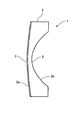
- FIG. 1 is a schematic view of the optical member with an antireflection film of the present embodiment.
- the optical member 1 with an antireflection film shown in FIG. 1 includes a base material 2 and an antireflection film 3 formed on the surface 2a of the base material 2.
- the base material 2 is glass, plastic, or the like, and is particularly preferably glass.
- the base material 2 is, for example, a glass lens for a surveillance camera or an in-vehicle camera.
- the surface of the base material 2 on which the antireflection film 3 is formed is, for example, an aspherical surface.
- the base material 2 in FIG. 1 is, for example, a meniscus lens having a negative power, but may be a meniscus lens having a positive power, a biconvex lens, a biconcave lens, or the like.
- the antireflection film 3 is formed on the surface 2a of the base material 2, but may be formed on both the surfaces 2a and 2b. Hereinafter, the antireflection film 3 will be described in more detail.
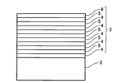
- the low refractive index layer 4 and the high refractive index layer 5 are alternately laminated from the surface (optical surface) of the base material 2, and the uppermost layer is formed. It is the outermost surface layer 6 that comes into contact with the outside air.
- Each low refractive index layer 4 has a lower refractive index than each high refractive index layer 5.
- the high refractive index layer 5 may be higher than the refractive index of the base material 2. Further, the antireflection film 3 is adjusted so that the reflectance is lower than that of the base material 2 alone.
- the density of the low refractive index layer 4 is 2.1 g / cm 3 or more and 2.2 g / cm 3 or less. If the upper limit of the density range is exceeded, the desired low refractive index cannot be obtained (the refractive index becomes too high), and if it is lower than the lower limit, the number of voids increases. If there are too many voids, water will enter the voids and affect the characteristics of the film, or the voids will reduce the adhesion of the film.
- the density of the low refractive index layer 4 is more it is preferably at most 2.132g / cm 3 or more 2.199g / cm 3, is 2.132g / cm 3 or more 2.191g / cm 3 or less It is preferable that it is 2.158 g / cm 3 or more and 2.174 g / cm 3 or less.
- the ion assisted deposition (IAD) method when the low refractive index layer 4 is formed by the thin film deposition method, the ion assisted deposition (IAD) method is not used.
- the high refractive index layer 5 is formed by the vapor deposition method, the ion-assisted vapor deposition method is used. Thereby, the density of the low refractive index layer 4 can be lowered within the above range.
- the density of the high refractive index layer 5 is higher by using the ion-assisted vapor deposition method than in the case where the ion-assisted vapor deposition method is not used.
- the low refractive index layer 4 can be adjusted to a relatively low density, whereby the refractive index of the low refractive index layer 4 can be reduced.
- the refractive index (wavelength 550 nm) of the low refractive index layer 4 is 1.41 or more and 1.47 or less, preferably 1.4245 or more and 1.469 or less, and more preferably 1. It is 4245 or more and 1.464 or less, and more preferably 1.4425 or more and 1.4525 or less.
- the spectral reflectance in the wavelength range of 400 nm or more and 1000 nm or less can be suppressed to 1% or less.
- the spectral reflectance at a wavelength of 410 nm to 430 nm can be set to 0.8% or less.
- the spectral reflectance at a wavelength of 480 nm to 600 nm can be set to 0.5 or less, and the spectral reflectance at a wavelength of 650 nm to 1000 nm can be set to 0.8 or less. is there.
- the total number of the low refractive index layer 4 and the high refractive index layer 5 is not limited, but it is preferably about 9 to 19 layers, and more preferably 11 to 15 layers. Is.
- the wavelength range in which the spectral reflectance is 1% or less can be widened, but when the low refractive index layer 4 is formed by the ion-assisted vapor deposition method, the spectral reflectance is 1% or less. It is known from the experiments described later that the wavelength range of the reflectance cannot be expanded to a wavelength of 1000 nm.
- the present inventors have formed a film of the low refractive index layer 4 without using the ion-assisted vapor deposition method to reduce the density of the low refractive index layer 4 as compared with the conventional case, thereby achieving a spectral reflectance of 1% or less.
- the low refractive index layer 4 is used as the bottom layer in contact with the surface of the base material 2, but the bottom layer can be appropriately selected from the viewpoint of adhesion to the base material 2. That is, it is arbitrary whether or not the low refractive index layer 4 is used as the lowermost layer.
- the low refractive index layer 4 is preferably formed by mixing layer comprising a single layer or SiO 2 in SiO 2.
- the materials of the plurality of low refractive index layers 4 laminated on the antireflection film 3 may be the same or different.
- the high refractive index layer 5 includes ZrO x (x is 1.5 to 2), TiO x (x is 1 to 2), and TaO x (x is 2 to 2.5).
- NbO x (x is 2 to 2.5) preferably a single layer or a mixed layer containing two or more kinds. It is preferable to use ZrO 2 for ZrO x , Ti 3 O 5 and Ti 2 O 5 for TiO x , Ta 2 O 5 for TaO x , and Nb 2 O 5 for NbO x .
- the above-mentioned metal oxide does not have to have a stoichiometric composition as long as the oxygen composition ratio is in the above-mentioned range of x.
- the materials of the plurality of high refractive index layers 5 laminated in the antireflection film 3 may be the same or different.
- the outermost surface layer 6 of the antireflection film 3 is preferably a single layer of MgF 2, a single layer of SiO 2 , or a mixed layer containing at least one of MgF 2 and SiO 2. ..
- the outermost surface layer 6 is an adjusting layer for suppressing the reflectance of the antireflection film 3 in which the low refractive index layer 4 and the high refractive index layer 5 are laminated within a predetermined value. That is, the outermost surface layer 6 can be provided as the uppermost layer of the low refractive index layer 4 and the high refractive index layer 5, and the reflectance can be optimized.
- MgF 2 for the outermost surface layer 6 from the viewpoint of adjusting the reflectance.
- Table 1 the refractive index of MgF 2 can be lower than that of SiO 2 .
- the film density was calculated using the following formula (1) using the refractive index and density of the evaporator.
- Membrane density (refractive index of film / refractive index of evaporator) x theoretical density of evaporator (1)
- the refractive index is MgF 2 ⁇ SiO 2 , but in the present embodiment, from the viewpoint of reliability and adhesion between layers, the low refractive index layer 4 has more SiO than MgF 2. 2 is preferably used, and MgF 2 is preferably used for the outermost surface layer 6 as the refractive index adjusting layer of the antireflection film 3.
- the low refractive index layer 4 is formed by vapor deposition without using the ion assisted vapor deposition method
- the high refractive index layer 5 is formed by the ion assisted vapor deposition method.
- the low refractive index layer 4 can be formed with a low density
- the high refractive index layer 5 can be formed with a high density.
- the "high density” and the “low density” mean the densities compared in each layer depending on whether or not the ion-assisted vapor deposition method is applied.
- the atmosphere when the low refractive index layer 4 is vapor-deposited is not limited, for example, oxygen, argon, nitrogen alone, or a mixed atmosphere thereof is preferable.
- the film forming pressure when forming the low refractive index layer 4 in the range of 3 ⁇ 10 -3 Pa to 8 ⁇ 10 -2 Pa.
- the film forming pressure is more preferably 3 ⁇ 10 -3 Pa to 5.8 ⁇ 10 -2 Pa, and further preferably 7.8 ⁇ 10 -3 Pa to 5.8 ⁇ 10 -2 Pa. It is preferably 1.5 ⁇ 10 -2 Pa to 3.2 ⁇ 10 -2 Pa, even more preferably.
- the density of the formed low refractive index layer 4 is adjusted to 2.1 g / cm 3 or more and 2.2 g / cm 3 or less, preferably 2.132 g / cm 3 to 2.199 g / cm 3 , more preferably.
- the evaporation material of the low refractive index layer 4 it is preferable to use a mixed material containing a simple substance or SiO 2 in SiO 2.
- the evaporation material of the high refractive index layer 5 a single substance or a mixed material containing two or more selected from ZrO 2 , Ti 3 O 5 , Ta 2 O 5 , and Nb 2 O 5 is used. It is preferable to use it.
- the evaporation material of the outermost surface layer 6 it is preferable to use a simple substance selected from MgF 2 and SiO 2 or a mixed material containing two or more kinds. It is preferable to select MgF 2 as the evaporation material of the outermost surface layer 6.
- the density of the low refractive index layer 4 can be lowered, and the refractive index can be lowered. Then, in the present embodiment, the spectral reflectance can be suppressed to 1% or less in the wavelength range of 400 nm to 1000 nm. Further, according to the optical member 1 with an antireflection film of the present embodiment, the adhesion of each layer is excellent, peeling and cracking are unlikely to occur even in a high temperature and high humidity environment, and high reliability can be obtained.
- the method for manufacturing the optical member 1 with an antireflection film of the present embodiment it is possible to control whether or not the ion-assisted vapor deposition method is applied when the low refractive index layer 4 and the high refractive index layer 5 are formed. Therefore, it is possible to easily manufacture the optical member 1 with an antireflection film which has an excellent antireflection function and has high reliability.
- the use time of the ion gun can be reduced when forming the antireflection film 3, and therefore, during the film formation.
- the temperature change can be reduced. This makes it possible to reduce the variation in the light reflection characteristics of the film-formed antireflection film 3.
- Examples 1 to 3 In Examples 1 to 3, the materials shown in Table 2 below are used, and in Comparative Examples, the materials shown in Table 3 below are used, and SiO 2 shown in Tables 2 and 3 is used as a low refractive index layer, Ta 2 O 5 was formed as a high refractive index layer and MgF 2 was formed as the outermost surface layer to obtain an antireflection film.
- the base material is a lens molded using BACD14 glass (manufactured by HOYA Corporation).
- Example 1 when the low refractive index layer was formed, it was formed by a vacuum vapor deposition method without ion-assisted vapor deposition.
- Table 2 in Example 1, the density of SiO 2 was 2.191 g / cm 3 , in Example 2, the density of SiO 2 was 2.158 g / cm 3 , and in Example 3, SiO 2 was used. The density of was 2.132 g / cm 3 .
- Table 4 The pressures during film formation in vacuum vapor deposition to obtain these densities are shown in Table 4 below. As shown in Table 4, the density can be changed by changing the film forming pressure.
- SiO 2 was formed into a film by an ion-assisted vapor deposition method.
- the data “with IAD” shown in Table 4 is applied to the comparative example.
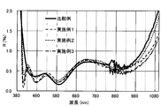
- the relationship between wavelength and reflectance was investigated using Examples 1 to 3 and Comparative Examples.
- the reflectance was measured by a microscope-type spectrophotometer (USPM-RUIII) manufactured by Olympus Corporation. In the experiment, the spectral reflectance of the incident light beam with the incident angle set to 0 ° was measured.
- FIG. 3 is a graph showing the relationship between wavelength and reflectance in Examples 1 to 3 and Comparative Example.
- the wavelength range of the spectral reflectance R of 1% or less can be widened as compared with Comparative Examples. Specifically, in the examples, it was found that the spectral reflectance can be reduced to 1% or less in the wavelength range of 400 nm to 1000 nm. Further, in the examples, it was found that the spectral reflectance at a wavelength of 480 nm to 600 nm can be set to 0.5 or less, and the spectral reflectance at a wavelength of 650 nm to 1000 nm can be set to 0.8 or less.
- the film forming pressure was set to 3 ⁇ 10 -3 Pa to 8 ⁇ 10 -2 Pa, preferably 3 ⁇ 10 -3 Pa to 5.8 ⁇ 10 -2 Pa. It was preferably 7.8 ⁇ 10 -3 Pa to 5.8 ⁇ 10 -2 Pa, and more preferably 1.5 ⁇ 10 -2 Pa to 3.2 ⁇ 10 -2 Pa.
- the density of the low refractive index layer is 2.1 g / cm 3 to 2.2 g / cm 3 , preferably 2.132 g / cm 3 to 2.199 g / cm 3, and more preferably 2.132 g. It was set to / cm 3 to 2.191 g / cm 3, and more preferably 2.158 g / cm 3 to 2.174 g / cm 3 .
- the refractive index (wavelength 550 nm) of the low refractive index layer is 1.41 to 1.47, preferably 1.4245 to 1.469, more preferably 1.4245 to 1.4640, and further. Preferably, it was 1.4425 to 1.4525.
- the SiO 2 (low refractive index layer) is formed by the ion-assisted vapor deposition method as in the comparative example
- the base material during the film formation is heated by the radiant heat of the ion gun, and the temperature changes during the film formation.
- the usage time of the ion gun can be reduced, and therefore the temperature change during the film formation can be reduced. I found that I could make it smaller. It was found that the variation in the characteristics of the film-formed antireflection film can be reduced by reducing the temperature change during film formation as in this example.
- Example 2 a high temperature and high humidity test was performed using Example 2.
- the experimental conditions were a temperature of 60 °, a humidity of 90%, and an experimental time of 240 hours. After the test, no appearance abnormality such as peeling or cracking was observed. As a result, a highly reliable optical member with an antireflection film could be obtained.
- the optical member with an antireflection film of the present invention can be preferably applied to a glass lens for an in-vehicle camera or the like.
Landscapes
- Chemical & Material Sciences (AREA)
- Physics & Mathematics (AREA)
- Organic Chemistry (AREA)
- Materials Engineering (AREA)
- Mechanical Engineering (AREA)
- Metallurgy (AREA)
- Engineering & Computer Science (AREA)
- Chemical Kinetics & Catalysis (AREA)
- General Physics & Mathematics (AREA)
- Optics & Photonics (AREA)
- Inorganic Chemistry (AREA)
- Surface Treatment Of Optical Elements (AREA)
- Physical Vapour Deposition (AREA)
Abstract
波長域400nm~1000nmにおいて、優れた反射防止機能を有する且高信頼性を持つ反射防止膜付き光学部材及びその製造方法を提供すること。本発明は、基材(2)の表面に、反射防止膜(3)が形成された反射防止膜付き光学部材であって、前記反射防止膜は、低屈折率層(4)と高屈折率層(5)と が交互に積層されており、前記低屈折率層の密度は、2.1g/cm3以上2.2g/cm3以下であることを特徴とする。前記低屈折率層の屈折率(波長550nm)は、1.41~1.47であることが好ましい。
Description
本発明は、反射防止膜付き光学部材及びその製造方法に関する。
レンズ等の光学部品では、表面に反射防止膜を設けることが一般的に行われている。反射防止膜は、例えば、特許文献1に記載するように、屈折率の異なる複数の層を積層して形成される。特許文献1では、各層の屈折率を、適宜調整することで、可視光領域から近赤外線領域の屈折率を更に低くでき、反射防止帯域を更に広くすることができるとしている。
特許文献1では、波長域380nm~980nmの反射率を1%以下にできるとしているが、近年のニーズから、反射防止機能を、波長域1000nmまで広くしたいうえ、コートの高温高湿などの信頼性も厳しく要求されている。
本発明は、以上の問題意識に基づいてなされたものであり、波長域400nm~1000nmにおいて、優れた反射防止機能を有し、且つ、高信頼性を持つ反射防止膜付き光学部材及びその製造方法を提供することを目的とする。
本発明は、基材の表面に、反射防止膜が形成された反射防止膜付き光学部材であって、前記反射防止膜は、低屈折率層と高屈折率層とが交互に積層されており、前記低屈折率層の密度は、2.1g/cm3以上2.2g/cm3以下であることを特徴とする。
本発明では、前記低屈折率層の屈折率(波長550nm)は、1.41~1.47であることが好ましい。
本発明では、前記低屈折率層は、SiO2の単層又はSiO2を含む混合層で形成されることが好ましい。
本発明では、前記反射防止膜の最表面層は、MgF2の単層、SiO2の単層、又は、MgF2及びSiO2の少なくとも一方を含む混合層であることが好ましい。
本発明では、400nm以上1000nm以下の波長域での分光反射率が、1%以下であることが好ましい。
本発明は、基材の表面に、低屈折率層と高屈折率層とを交互に積層して反射防止膜を成膜する反射防止膜付き光学部材の製造方法であって、前記低屈折率層を、イオンアシスト蒸着法を用いずに蒸着により成膜し、前記高屈折率層を、イオンアシスト蒸着法により成膜することが好ましい。
本発明では、前記低屈折率層を成膜する際の成膜時圧力を、3×10⁻³Pa以上8×10⁻²Pa以下の範囲で調整することが好ましい。
本発明では、前記低屈折率層の蒸発材料として、SiO2の単体又はSiO2を含む混合材を用いることが好ましい。
本発明によれば、波長域400nm~1000nmにおいて、分光反射率を1%以下に抑えることができる。
以下、本発明を実施するための形態(以下、単に「本実施形態」という。)について詳細に説明する。なお、以下では、「~」を使用する場合があるが、その下限値及び上限値は、いずれも含むものとする。
<反射防止膜付き光学部材>
本発明者らは、反射防止膜付き光学部材の反射防止機能を鋭意研究した結果、低屈折率層の密度を調節することで、波長域400nm~1000nmにおいて、優れた反射防止機能を有し、且つ、高信頼性を持つ反射防止膜付き光学部材を開発するに至った。すなわち、本実施形態の反射防止膜付き光学部材は、反射防止膜が、低屈折率層と高屈折率層との積層構造であり、低屈折率層の密度が、2.1g/cm3以上2.2g/cm3以下であることを特徴とする。
本発明者らは、反射防止膜付き光学部材の反射防止機能を鋭意研究した結果、低屈折率層の密度を調節することで、波長域400nm~1000nmにおいて、優れた反射防止機能を有し、且つ、高信頼性を持つ反射防止膜付き光学部材を開発するに至った。すなわち、本実施形態の反射防止膜付き光学部材は、反射防止膜が、低屈折率層と高屈折率層との積層構造であり、低屈折率層の密度が、2.1g/cm3以上2.2g/cm3以下であることを特徴とする。
図1は、本実施形態の反射防止膜付き光学部材の模式図である。図1に示す反射防止膜付き光学部材1は、基材2と、基材2の表面2aに形成された反射防止膜3と、を有して構成される。
基材2は、ガラスやプラスチック等であり、特に、ガラスであることが好ましい。特に限定されるものでないが、基材2は、例えば、監視カメラや車載カメラ用のガラスレンズである。また、反射防止膜3が成膜される基材2の表面は、例えば、非球面である。図1の基材2は、例えば、負のパワーを有するメニスカスレンズであるが、正のパワーを有するメニスカスレンズであってもよいし、両凸レンズあるいは両凹レンズ等でもよい。
図1では、反射防止膜3は、基材2の表面2aに成膜されるが、表面2a、2bの双方に形成されてもよい。
以下、反射防止膜3について、更に詳しく説明する。
以下、反射防止膜3について、更に詳しく説明する。
<反射防止膜>
図2に示すように、本実施形態の反射防止膜3は、基材2の表面(光学面)から、低屈折率層4と高屈折率層5とが交互に積層され、最上層が、外気と触れる最表面層6となっている。
図2に示すように、本実施形態の反射防止膜3は、基材2の表面(光学面)から、低屈折率層4と高屈折率層5とが交互に積層され、最上層が、外気と触れる最表面層6となっている。
各低屈折率層4は、各高屈折率層5よりも屈折率が低い。一方、高屈折率層5は、基材2の屈折率より高くてもよい。また、反射防止膜3は、基材2単体の場合よりも反射率が低くなるように調整される。
低屈折率層4の密度は、2.1g/cm3以上2.2g/cm3以下である。密度範囲の上限を上回ると所望の低屈折率が得られず(屈折率が高くなりすぎる)、下限を下回ると空隙が多くなる。空隙が多くなりすぎると空隙に水分が入って膜の特性に影響を及ぼしたり、空隙のために膜の密着性が低下する。また、低屈折率層4の密度は、2.132g/cm3以上2.199g/cm3以下であることが好ましく、2.132g/cm3以上2.191g/cm3以下であることがより好ましく、2.158g/cm3以上2.174g/cm3以下であることが更に好ましい。
本実施の形態では、後述するように、低屈折率層4を蒸着法にて成膜する際、イオンアシスト蒸着(Ion Assisted Deposition:IAD)法を用いない。一方、高屈折率層5を蒸着法にて成膜する際、イオンアシスト蒸着法を用いる。これにより、低屈折率層4の密度を、上記範囲内に低くすることが可能である。なお、高屈折率層5の密度は、イオンアシスト蒸着法を用いることで、イオンアシスト蒸着法を用いない場合と比べて、高くなる。
本実施の形態では、低屈折率層4を比較的低い密度に調整することができ、これにより、低屈折率層4の屈折率を、小さくすることができる。具体的には、低屈折率層4の屈折率(波長550nm)は、1.41以上1.47以下であり、好ましくは、1.4245以上1.469以下であり、より好ましくは、1.4245以上1.464以下であり、更に好ましくは、1.4425以上1.4525以下である。
このように、低屈折率層4の密度及び屈折率を、上記範囲内に低く抑えることで、400nm以上1000nm以下の波長域での分光反射率を、1%以下に抑えることできる。本実施の形態では、波長410nm~430nmの分光反射率を、0.8%以下とすることができる。また、本実施の形態では、好ましくは、波長480nm~600nmの分光反射率を、0.5以下にでき、更に、波長650nm~1000nmの分光反射率を、0.8以下にすることが可能である。
本実施の形態では、低屈折率層4と高屈折率層5とを合わせた総数を限定するものでないが、好ましくは、9層~19層程度であり、より好ましくは、11層~15層である。層数を増やすことで、分光反射率が、1%以下となる波長域を広げることができるが、低屈折率層4を、イオンアシスト蒸着法を用いて成膜すると、1%以下の分光反射率となる波長域を、波長1000nmまで広げられないことが後述の実験によりわかっている。そこで、本発明者らは、低屈折率層4を、イオンアシスト蒸着法を用いずに成膜し、低屈折率層4の密度を従来より低減させることで、1%以下の分光反射率となる波長域を、波長1000nmまで広げることに成功している。
また、図1では、基材2の表面と接する最下層に低屈折率層4を用いたが、基材2との密着性の観点から、最下層を適宜選択することができる。すなわち、最下層として、低屈折率層4を用いるか否かは任意である。
次に、低屈折率層4及び高屈折率層5の好ましい材質について説明する。
本実施形態では、低屈折率層4は、SiO2の単層又はSiO2を含む混合層で形成されることが好ましい。反射防止膜3に積層される複数の低屈折率層4の材質は、同一であっても異なっていてもよい。
本実施形態では、低屈折率層4は、SiO2の単層又はSiO2を含む混合層で形成されることが好ましい。反射防止膜3に積層される複数の低屈折率層4の材質は、同一であっても異なっていてもよい。
また、本実施形態では、高屈折率層5は、ZrOx(xは、1.5~2)、TiOx(xは、1~2)、TaOx(xは、2~2.5)、及び、NbOx(xは、2~2.5)から選択される単層又は2種以上を含む混合層で形成されることが好ましい。ZrOxには、ZrO2、TiOxには、Ti3O5、Ti2O5、TaOxには、Ta2O5、NbOxには、Nb2O5を用いることが好ましい。上記した金属酸化物は、化学量論組成でなくても、酸素の組成比率が上記xの範囲であればよい。
反射防止膜3内に積層される複数の高屈折率層5の材質は、同一であっても異なっていてもよい。
また、本実施の形態では、反射防止膜3の最表面層6は、MgF2の単層、SiO2の単層、又は、MgF2及びSiO2の少なくとも一方を含む混合層であることが好ましい。最表面層6は、低屈折率層4と高屈折率層5とが積層された反射防止膜3の反射率を所定値内に抑えるための調整層である。すなわち、低屈折率層4と高屈折率層5の最上層として最表面層6を設けて、反射率を適正化することができる。例えば、低屈折率層4としてSiO2を用い、高屈折率層5としてTa2O5を用いた構成では、最表面層6にMgF2を用いることが、反射率の調整の観点から好適である。以下の表1に示すように、MgF2の屈折率は、SiO2より低くすることができる。

なお、膜密度は、蒸発材の屈折率と密度とを使用し、下記の式(1)を用いて計算した。
膜密度=(膜の屈折率/蒸発材の屈折率)×蒸発材の理論密度 (1)
膜密度=(膜の屈折率/蒸発材の屈折率)×蒸発材の理論密度 (1)
表1に示すように、屈折率は、MgF2<SiO2であるが、本実施の形態では、信頼性や各層間の密着性の観点から、低屈折率層4には、MgF2よりSiO2を用いることが好ましく、反射防止膜3の反射率の調整層として、最表面層6にMgF2を用いることが好適である。
<反射防止膜付き光学部材の製造方法>
図2に示す本実施形態の反射防止膜付き光学部材の製造方法について説明する。
本実施形態では、基材2の表面に、低屈折率層4と高屈折率層5とを交互に積層し、反射防止膜3を形成する。
図2に示す本実施形態の反射防止膜付き光学部材の製造方法について説明する。
本実施形態では、基材2の表面に、低屈折率層4と高屈折率層5とを交互に積層し、反射防止膜3を形成する。
このとき、低屈折率層4を、イオンアシスト蒸着法を用いずに蒸着により成膜し、高屈折率層5を、イオンアシスト蒸着法により成膜する。
これにより、低屈折率層4を、低い密度で成膜でき、高屈折率層5を、高い密度で成膜することができる。ここで、「高い密度」、「低い密度」とは、各層において、イオンアシスト蒸着法の適用有無により比較された密度を意味する。
低屈折率層4を蒸着する際の雰囲気を制限するものではないが、例えば、酸素、アルゴン、或いは、窒素単体、又は、これらの混合雰囲気であることが好ましい。
また、本実施の形態では、低屈折率層4を成膜する際の成膜時圧力を、3×10⁻³Pa~8×10⁻²Paの範囲で調整することが好ましい。成膜時圧力を、3×10⁻³Pa~5.8×10⁻²Paとすることがより好ましく、7.8×10⁻³Pa~5.8×10⁻²Paとすることが更に好ましく、1.5×10⁻²Pa~3.2×10⁻²Paとすることが更により好ましい。
これにより、成膜された低屈折率層4の密度を、2.1g/cm3以上2.2g/cm3以下、好ましくは、2.132g/cm3~2.199g/cm3、より好ましくは、2.132g/cm3~2.191g/cm3、更に好ましくは、2.158g/cm3~2.174g/cm3とすることができる。
本実施形態では、低屈折率層4の蒸発材料として、SiO2の単体又はSiO2を含む混合材を用いることが好ましい。
また、本実施形態では、高屈折率層5の蒸発材料として、ZrO2、Ti3O5、Ta2O5、及び、Nb2O5から選択される単体又は2種以上を含む混合材を用いることが好ましい。
また、本実施の形態では、最表面層6の蒸発材料として、MgF2、及び、SiO2から選択される単体又は2種以上を含む混合材を用いることが好ましい。最表面層6の蒸発材料として、MgF2を選択することが好ましい。
以上、詳述した本実施の形態の反射防止膜付き光学部材1によれば、低屈折率層4の密度を下げることができ、屈折率を低下させることができる。そして、本実施の形態では、波長域400nm~1000nmにおいて、分光反射率を1%以下に抑えることができる。また、本実施の形態の反射防止膜付き光学部材1によれば、各層の密着性に優れるとともに、高温多湿の環境下においても、剥離やクラックが生じにくく、高い信頼性を得ることができる。
また、本実施の形態の反射防止膜付き光学部材1の製造方法によれば、低屈折率層4及び高屈折率層5を成膜するに際し、イオンアシスト蒸着法の適用の有無を制御することで、優れた反射防止機能を有し、且つ、高信頼性を持つ反射防止膜付き光学部材1を簡単に製造できる。
また、本実施の形態では低屈折率層を、イオンアシスト蒸着せずに成膜するため、反射防止膜3を成膜するに際し、イオンガンの使用時間を減少することができ、したがって、成膜中の温度変化を小さくすることができる。これにより、成膜された反射防止膜3の光反射特性のばらつきを小さくすることが可能である。
以下、本実施形態を実施例及び比較例を用いてより具体的に説明する。実験では、以下に示す実施例1から実施例3及び比較例を製造した。
[実施例1~実施例3]
実施例1~実施例3では、以下の表2に示す材料を用い、比較例では、以下の表3に示す材料を用い、表2、表3に示すSiO2を低屈折率層、Ta2O5を高屈折率層、MgF2を最表面層として成膜し、反射防止膜を得た。なお、基材は、BACD14ガラス(HOYA(株)製)を用いて成形したレンズである。
実施例1~実施例3では、以下の表2に示す材料を用い、比較例では、以下の表3に示す材料を用い、表2、表3に示すSiO2を低屈折率層、Ta2O5を高屈折率層、MgF2を最表面層として成膜し、反射防止膜を得た。なお、基材は、BACD14ガラス(HOYA(株)製)を用いて成形したレンズである。


表2に示す実施例1から実施例3では、低屈折率層を成膜する際、真空蒸着法にて、イオンアシスト蒸着なしで成膜した。表2に示すように、実施例1では、SiO2の密度を、2.191g/cm3、実施例2では、SiO2の密度を、2.158g/cm3、実施例3では、SiO2の密度を、2.132g/cm3とした。これらの密度を得るための真空蒸着における成膜時圧力は、以下の表4に示されている。表4に示すように、成膜時圧力を変えることで、密度を変化させることができる。

一方、比較例では、SiO2を、イオンアシスト蒸着法にて成膜した。表4に示す「IADあり」のデータは、比較例に適用される。
実施例1から実施例3及び比較例を用いて、波長と反射率との関係を調べた。反射率は、オリンパス(株)製の顕微鏡型分光測定機(USPM―RUIII)により測定した。実験では、入射角を0°とした入射光線の分光反射率を測定した。
図3は、実施例1~実施例3及び比較例における波長と反射率との関係を示すグラフである。
図3に示すように、実施例1~実施例3は、比較例に比べて、1%以下となる分光反射率Rの波長域を広げることができるとわかった。具体的には、実施例では、400nm~1000nmの波長域にて、分光反射率を1%以下にできるとわかった。また実施例では、波長480nm~600nmの分光反射率を、0.5以下にでき、更に、波長650nm~1000nmの分光反射率を、0.8以下にできることがわかった。
表4の実験結果に基づいて、好ましい成膜時圧力、密度及び屈折率を求めた。すなわち、表4に示すように、SiO2を、イオンアシスト蒸着なしで成膜したとき、成膜時圧力を8.2×10⁻²Paとすると、密度は、2.098とかなり小さくなり、低屈折率層に空孔が生じやすいことがわかった。このため、表4の実験結果により、成膜時圧力を、3×10⁻³Pa~8×10⁻²Pa、好ましくは、3×10⁻³Pa~5.8×10⁻²Pa、より好ましくは、7.8×10⁻³Pa~5.8×10⁻²Pa、更に好ましくは、1.5×10⁻²Pa~3.2×10⁻²Paとした。
また、低屈折率層の密度は、2.1g/cm3~2.2g/cm3とし、好ましくは、2.132g/cm3~2.199g/cm3とし、より好ましくは、2.132g/cm3~2.191g/cm3とし、更に好ましくは、2.158g/cm3~2.174g/cm3とした。
また、低屈折率層の屈折率(波長550nm)は、1.41~1.47とし、好ましくは、1.4245~1.469とし、より好ましくは、1.4245~1.4640とし、更に好ましくは、1.4425~1.4525とした。
また、比較例のように、SiO2(低屈折率層)を、イオンアシスト蒸着法により成膜する場合、イオンガンの輻射熱により、成膜中の基材は加熱されて、成膜中の温度変化が大きくなることがわかった。一方、本実施例のように、SiO2(低屈折率層)を、イオンアシスト蒸着せずに成膜する場合、イオンガンの使用時間を減少することができ、したがって、成膜中の温度変化を小さくすることができるとわかった。本実施例のように、成膜中の温度変化を小さくできることで、成膜された反射防止膜の特性ばらつきを小さくすることができるとわかった。
次に、実施例2を用いて、高温多湿試験を行った。実験条件は、温度60°、湿度90%、実験時間240時間とした。試験後、剥離やクラック等の外観異常は見られなかった。これにより、高信頼性の反射防止膜付き光学部材を得ることができた。
本発明の反射防止膜付き光学部材を、車載カメラ用等のガラスレンズに好ましく適用することができる。
本出願は、2019年8月8日出願の特願2019-146114に基づく。この内容は全てここに含めておく。
Claims (8)
- 基材の表面に、反射防止膜が形成された反射防止膜付き光学部材であって、
前記反射防止膜は、低屈折率層と高屈折率層とが交互に積層されており、
前記低屈折率層の密度は、2.1g/cm3以上2.2g/cm3以下であることを特徴とする反射防止膜付き光学部材。 - 前記低屈折率層の屈折率(波長550nm)は、1.41~1.47であることを特徴とする請求項1に記載の反射防止膜付き光学部材。
- 前記低屈折率層は、SiO2の単層又はSiO2を含む混合層で形成されることを特徴とする請求項1又は請求項2に記載の反射防止膜付き光学部材。
- 前記反射防止膜の最表面層は、MgF2の単層、SiO2の単層、又は、MgF2及びSiO2の少なくとも一方を含む混合層であることを特徴とする請求項1から請求項3のいずれかに記載の反射防止膜付き光学部材。
- 400nm以上1000nm以下の波長域での分光反射率が、1%以下であることを特徴とする請求項1から請求項4のいずれかに記載の反射防止膜付き光学部材。
- 基材の表面に、低屈折率層と高屈折率層とを交互に積層して反射防止膜を成膜する反射防止膜付き光学部材の製造方法であって、
前記低屈折率層を、イオンアシスト蒸着法を用いずに蒸着により成膜し、前記高屈折率層を、イオンアシスト蒸着法により成膜することを特徴とする反射防止膜付き光学部材の製造方法。 - 前記低屈折率層を成膜する際の成膜時圧力を、3×10⁻³Pa以上8×10⁻²Pa以下の範囲で調整することを特徴とする反射防止膜付き光学部材の製造方法。
- 前記低屈折率層の蒸発材料として、SiO2の単体又はSiO2を含む混合材を用いることを特徴とする請求項6又は請求項7に記載の反射防止膜付き光学部材の製造方法。
Priority Applications (1)
| Application Number | Priority Date | Filing Date | Title |
|---|---|---|---|
| CN202080043467.8A CN113966409A (zh) | 2019-08-08 | 2020-07-27 | 带有防反射膜的光学构件及其制造方法 |
Applications Claiming Priority (2)
| Application Number | Priority Date | Filing Date | Title |
|---|---|---|---|
| JP2019146114A JP2021026163A (ja) | 2019-08-08 | 2019-08-08 | 反射防止膜付き光学部材及びその製造方法 |
| JP2019-146114 | 2019-08-08 |
Publications (1)
| Publication Number | Publication Date |
|---|---|
| WO2021024834A1 true WO2021024834A1 (ja) | 2021-02-11 |
Family
ID=74503600
Family Applications (1)
| Application Number | Title | Priority Date | Filing Date |
|---|---|---|---|
| PCT/JP2020/028713 WO2021024834A1 (ja) | 2019-08-08 | 2020-07-27 | 反射防止膜付き光学部材及びその製造方法 |
Country Status (3)
| Country | Link |
|---|---|
| JP (1) | JP2021026163A (ja) |
| CN (1) | CN113966409A (ja) |
| WO (1) | WO2021024834A1 (ja) |
Cited By (1)
| Publication number | Priority date | Publication date | Assignee | Title |
|---|---|---|---|---|
| CN113900165A (zh) * | 2021-11-16 | 2022-01-07 | 天津津航技术物理研究所 | 一种氟化钡基底复合增透膜及其结构设计方法 |
Families Citing this family (1)
| Publication number | Priority date | Publication date | Assignee | Title |
|---|---|---|---|---|
| CN113593408B (zh) * | 2021-07-07 | 2022-09-09 | 武汉华星光电半导体显示技术有限公司 | 显示模组及其制作方法、移动终端 |
Citations (11)
| Publication number | Priority date | Publication date | Assignee | Title |
|---|---|---|---|---|
| JP2004061879A (ja) * | 2002-07-29 | 2004-02-26 | Ito Kogaku Kogyo Kk | 表面保護膜を備えた光学要素 |
| JP2005338366A (ja) * | 2004-05-26 | 2005-12-08 | Olympus Corp | 反射防止膜及び光学部品 |
| JP2007127681A (ja) * | 2005-11-01 | 2007-05-24 | Tokai Kogaku Kk | プラスチックレンズ |
| JP2007298951A (ja) * | 2006-04-04 | 2007-11-15 | Seiko Epson Corp | 光学多層膜フィルタ、光学多層膜フィルタの製造方法および電子機器装置 |
| JP2009109850A (ja) * | 2007-10-31 | 2009-05-21 | Toppan Printing Co Ltd | 反射防止フィルム及びその製造方法並びに反射防止フィルムを用いた偏光板及びその製造方法 |
| JP2009139925A (ja) * | 2007-11-16 | 2009-06-25 | Epson Toyocom Corp | 光学多層膜フィルタ、光学多層膜フィルタの製造方法および電子機器装置 |
| JP2010102157A (ja) * | 2008-10-24 | 2010-05-06 | Seiko Epson Corp | 光学物品およびその製造方法 |
| JP2010519586A (ja) * | 2007-02-23 | 2010-06-03 | エシロール アテルナジオナール カンパニー ジェネラーレ デ オプティック | 接着性および耐摩耗性が改善された非反射または反射コーティングで被覆された光学製品の製造方法 |
| JP2010140008A (ja) * | 2008-11-13 | 2010-06-24 | Seiko Epson Corp | 光学物品およびその製造方法 |
| JP2012027412A (ja) * | 2010-07-28 | 2012-02-09 | Konica Minolta Opto Inc | 光学素子およびその製造方法 |
| JP2012118536A (ja) * | 2009-10-09 | 2012-06-21 | Seiko Epson Corp | 光学物品、光学物品の製造方法、電子機器 |
Family Cites Families (4)
| Publication number | Priority date | Publication date | Assignee | Title |
|---|---|---|---|---|
| JP2004163549A (ja) * | 2002-11-11 | 2004-06-10 | Pentax Corp | 反射防止膜 |
| JP5777278B2 (ja) * | 2009-12-01 | 2015-09-09 | キヤノン株式会社 | 光学素子の製造方法 |
| JP5893271B2 (ja) * | 2011-06-10 | 2016-03-23 | オリンパス株式会社 | 反射防止膜、光学系、及び光学機器 |
| JP6234857B2 (ja) * | 2014-03-24 | 2017-11-22 | 富士フイルム株式会社 | 反射防止機能付きレンズの製造方法 |
-
2019
- 2019-08-08 JP JP2019146114A patent/JP2021026163A/ja active Pending
-
2020
- 2020-07-27 CN CN202080043467.8A patent/CN113966409A/zh active Pending
- 2020-07-27 WO PCT/JP2020/028713 patent/WO2021024834A1/ja active Application Filing
Patent Citations (11)
| Publication number | Priority date | Publication date | Assignee | Title |
|---|---|---|---|---|
| JP2004061879A (ja) * | 2002-07-29 | 2004-02-26 | Ito Kogaku Kogyo Kk | 表面保護膜を備えた光学要素 |
| JP2005338366A (ja) * | 2004-05-26 | 2005-12-08 | Olympus Corp | 反射防止膜及び光学部品 |
| JP2007127681A (ja) * | 2005-11-01 | 2007-05-24 | Tokai Kogaku Kk | プラスチックレンズ |
| JP2007298951A (ja) * | 2006-04-04 | 2007-11-15 | Seiko Epson Corp | 光学多層膜フィルタ、光学多層膜フィルタの製造方法および電子機器装置 |
| JP2010519586A (ja) * | 2007-02-23 | 2010-06-03 | エシロール アテルナジオナール カンパニー ジェネラーレ デ オプティック | 接着性および耐摩耗性が改善された非反射または反射コーティングで被覆された光学製品の製造方法 |
| JP2009109850A (ja) * | 2007-10-31 | 2009-05-21 | Toppan Printing Co Ltd | 反射防止フィルム及びその製造方法並びに反射防止フィルムを用いた偏光板及びその製造方法 |
| JP2009139925A (ja) * | 2007-11-16 | 2009-06-25 | Epson Toyocom Corp | 光学多層膜フィルタ、光学多層膜フィルタの製造方法および電子機器装置 |
| JP2010102157A (ja) * | 2008-10-24 | 2010-05-06 | Seiko Epson Corp | 光学物品およびその製造方法 |
| JP2010140008A (ja) * | 2008-11-13 | 2010-06-24 | Seiko Epson Corp | 光学物品およびその製造方法 |
| JP2012118536A (ja) * | 2009-10-09 | 2012-06-21 | Seiko Epson Corp | 光学物品、光学物品の製造方法、電子機器 |
| JP2012027412A (ja) * | 2010-07-28 | 2012-02-09 | Konica Minolta Opto Inc | 光学素子およびその製造方法 |
Cited By (2)
| Publication number | Priority date | Publication date | Assignee | Title |
|---|---|---|---|---|
| CN113900165A (zh) * | 2021-11-16 | 2022-01-07 | 天津津航技术物理研究所 | 一种氟化钡基底复合增透膜及其结构设计方法 |
| CN113900165B (zh) * | 2021-11-16 | 2023-09-22 | 天津津航技术物理研究所 | 一种氟化钡基底复合增透膜及其结构设计方法 |
Also Published As
| Publication number | Publication date |
|---|---|
| JP2021026163A (ja) | 2021-02-22 |
| CN113966409A (zh) | 2022-01-21 |
Similar Documents
| Publication | Publication Date | Title |
|---|---|---|
| US5993898A (en) | Fabrication method and structure for multilayer optical anti-reflection coating, and optical component and optical system using multilayer optical anti-reflection coating | |
| JP4854552B2 (ja) | 反射防止膜及びこれを有する光学部品 | |
| US20220221617A1 (en) | Curved surface films and methods of manufacturing the same | |
| JP4822786B2 (ja) | 反射防止膜及びこれを有する光学部品 | |
| JP6411517B2 (ja) | 反射防止膜および反射防止膜を備えた光学部材 | |
| WO2021024834A1 (ja) | 反射防止膜付き光学部材及びその製造方法 | |
| US20060245056A1 (en) | Thin-film structure with counteracting layer | |
| JP5072395B2 (ja) | 反射防止膜及びこれを有する光学部品 | |
| JP4612827B2 (ja) | 反射防止膜 | |
| JP5549342B2 (ja) | 反射防止膜、及びこれを有する光学部材 | |
| JP5292318B2 (ja) | 反射防止膜、及びこれを有する光学部材 | |
| US11204446B2 (en) | Anti-reflection film and an optical component containing the anti-reflection film | |
| JP7216471B2 (ja) | 車載レンズ用のプラスチックレンズ及びその製造方法 | |
| JP6989289B2 (ja) | 親水性反射防止膜付きレンズ及びその製造方法 | |
| JP7098129B2 (ja) | 反射防止膜及びこれを有する光学素子 | |
| US20200041694A1 (en) | Thin film forming method and porous thin film | |
| JP2000171607A (ja) | 高緻密な多層薄膜およびその成膜方法 | |
| JP2020190710A (ja) | 反射防止膜及びこれを有する光学素子 | |
| CN116819661A (zh) | 一种光谱特性可变的光学薄膜及其光谱特性的调节方法 | |
| JP7117081B2 (ja) | 防塵レンズ及びその製造方法 | |
| JP4051015B2 (ja) | 反射防止フィルム | |
| Liou et al. | Fabrication of wide-angle and wideband visible antireflection coating on flexible poly (ether sulfone) substrate using ion-assisted deposition | |
| JPS6296901A (ja) | 合成樹脂製レンズ | |
| JP2023037490A (ja) | 反射防止膜付き光学部材、及びその製造方法 | |
| JP2014174209A (ja) | 反射防止膜およびそれを有する光学素子並びに光学系 |
Legal Events
| Date | Code | Title | Description |
|---|---|---|---|
| 121 | Ep: the epo has been informed by wipo that ep was designated in this application |
Ref document number: 20849266 Country of ref document: EP Kind code of ref document: A1 |
|
| NENP | Non-entry into the national phase |
Ref country code: DE |
|
| 122 | Ep: pct application non-entry in european phase |
Ref document number: 20849266 Country of ref document: EP Kind code of ref document: A1 |