WO2020262385A1 - 入力装置 - Google Patents
入力装置 Download PDFInfo
- Publication number
- WO2020262385A1 WO2020262385A1 PCT/JP2020/024629 JP2020024629W WO2020262385A1 WO 2020262385 A1 WO2020262385 A1 WO 2020262385A1 JP 2020024629 W JP2020024629 W JP 2020024629W WO 2020262385 A1 WO2020262385 A1 WO 2020262385A1
- Authority
- WO
- WIPO (PCT)
- Prior art keywords
- electrode
- electrodes
- transmitting
- receiving
- input device
- Prior art date
Links
Images


Classifications
-
- G—PHYSICS
- G01—MEASURING; TESTING
- G01B—MEASURING LENGTH, THICKNESS OR SIMILAR LINEAR DIMENSIONS; MEASURING ANGLES; MEASURING AREAS; MEASURING IRREGULARITIES OF SURFACES OR CONTOURS
- G01B7/00—Measuring arrangements characterised by the use of electric or magnetic techniques
- G01B7/30—Measuring arrangements characterised by the use of electric or magnetic techniques for measuring angles or tapers; for testing the alignment of axes
-
- G—PHYSICS
- G01—MEASURING; TESTING
- G01D—MEASURING NOT SPECIALLY ADAPTED FOR A SPECIFIC VARIABLE; ARRANGEMENTS FOR MEASURING TWO OR MORE VARIABLES NOT COVERED IN A SINGLE OTHER SUBCLASS; TARIFF METERING APPARATUS; MEASURING OR TESTING NOT OTHERWISE PROVIDED FOR
- G01D5/00—Mechanical means for transferring the output of a sensing member; Means for converting the output of a sensing member to another variable where the form or nature of the sensing member does not constrain the means for converting; Transducers not specially adapted for a specific variable
- G01D5/12—Mechanical means for transferring the output of a sensing member; Means for converting the output of a sensing member to another variable where the form or nature of the sensing member does not constrain the means for converting; Transducers not specially adapted for a specific variable using electric or magnetic means
- G01D5/14—Mechanical means for transferring the output of a sensing member; Means for converting the output of a sensing member to another variable where the form or nature of the sensing member does not constrain the means for converting; Transducers not specially adapted for a specific variable using electric or magnetic means influencing the magnitude of a current or voltage
- G01D5/24—Mechanical means for transferring the output of a sensing member; Means for converting the output of a sensing member to another variable where the form or nature of the sensing member does not constrain the means for converting; Transducers not specially adapted for a specific variable using electric or magnetic means influencing the magnitude of a current or voltage by varying capacitance
-
- G—PHYSICS
- G01—MEASURING; TESTING
- G01R—MEASURING ELECTRIC VARIABLES; MEASURING MAGNETIC VARIABLES
- G01R25/00—Arrangements for measuring phase angle between a voltage and a current or between voltages or currents
-
- G—PHYSICS
- G06—COMPUTING; CALCULATING OR COUNTING
- G06F—ELECTRIC DIGITAL DATA PROCESSING
- G06F3/00—Input arrangements for transferring data to be processed into a form capable of being handled by the computer; Output arrangements for transferring data from processing unit to output unit, e.g. interface arrangements
- G06F3/01—Input arrangements or combined input and output arrangements for interaction between user and computer
- G06F3/03—Arrangements for converting the position or the displacement of a member into a coded form
- G06F3/033—Pointing devices displaced or positioned by the user, e.g. mice, trackballs, pens or joysticks; Accessories therefor
- G06F3/0362—Pointing devices displaced or positioned by the user, e.g. mice, trackballs, pens or joysticks; Accessories therefor with detection of 1D translations or rotations of an operating part of the device, e.g. scroll wheels, sliders, knobs, rollers or belts
-
- G—PHYSICS
- G06—COMPUTING; CALCULATING OR COUNTING
- G06F—ELECTRIC DIGITAL DATA PROCESSING
- G06F3/00—Input arrangements for transferring data to be processed into a form capable of being handled by the computer; Output arrangements for transferring data from processing unit to output unit, e.g. interface arrangements
- G06F3/01—Input arrangements or combined input and output arrangements for interaction between user and computer
- G06F3/03—Arrangements for converting the position or the displacement of a member into a coded form
- G06F3/033—Pointing devices displaced or positioned by the user, e.g. mice, trackballs, pens or joysticks; Accessories therefor
- G06F3/039—Accessories therefor, e.g. mouse pads
- G06F3/0393—Accessories for touch pads or touch screens, e.g. mechanical guides added to touch screens for drawing straight lines, hard keys overlaying touch screens or touch pads
-
- G—PHYSICS
- G06—COMPUTING; CALCULATING OR COUNTING
- G06F—ELECTRIC DIGITAL DATA PROCESSING
- G06F3/00—Input arrangements for transferring data to be processed into a form capable of being handled by the computer; Output arrangements for transferring data from processing unit to output unit, e.g. interface arrangements
- G06F3/01—Input arrangements or combined input and output arrangements for interaction between user and computer
- G06F3/03—Arrangements for converting the position or the displacement of a member into a coded form
- G06F3/041—Digitisers, e.g. for touch screens or touch pads, characterised by the transducing means
- G06F3/044—Digitisers, e.g. for touch screens or touch pads, characterised by the transducing means by capacitive means
- G06F3/0448—Details of the electrode shape, e.g. for enhancing the detection of touches, for generating specific electric field shapes, for enhancing display quality
-
- G—PHYSICS
- G05—CONTROLLING; REGULATING
- G05G—CONTROL DEVICES OR SYSTEMS INSOFAR AS CHARACTERISED BY MECHANICAL FEATURES ONLY
- G05G1/00—Controlling members, e.g. knobs or handles; Assemblies or arrangements thereof; Indicating position of controlling members
- G05G1/08—Controlling members for hand actuation by rotary movement, e.g. hand wheels
-
- G—PHYSICS
- G05—CONTROLLING; REGULATING
- G05G—CONTROL DEVICES OR SYSTEMS INSOFAR AS CHARACTERISED BY MECHANICAL FEATURES ONLY
- G05G5/00—Means for preventing, limiting or returning the movements of parts of a control mechanism, e.g. locking controlling member
- G05G5/06—Means for preventing, limiting or returning the movements of parts of a control mechanism, e.g. locking controlling member for holding members in one or a limited number of definite positions only
- G05G5/065—Means for preventing, limiting or returning the movements of parts of a control mechanism, e.g. locking controlling member for holding members in one or a limited number of definite positions only using a spring-loaded ball
-
- G—PHYSICS
- G06—COMPUTING; CALCULATING OR COUNTING
- G06F—ELECTRIC DIGITAL DATA PROCESSING
- G06F2203/00—Indexing scheme relating to G06F3/00 - G06F3/048
- G06F2203/041—Indexing scheme relating to G06F3/041 - G06F3/045
- G06F2203/04107—Shielding in digitiser, i.e. guard or shielding arrangements, mostly for capacitive touchscreens, e.g. driven shields, driven grounds
-
- H—ELECTRICITY
- H01—ELECTRIC ELEMENTS
- H01H—ELECTRIC SWITCHES; RELAYS; SELECTORS; EMERGENCY PROTECTIVE DEVICES
- H01H19/00—Switches operated by an operating part which is rotatable about a longitudinal axis thereof and which is acted upon directly by a solid body external to the switch, e.g. by a hand
- H01H19/02—Details
- H01H19/10—Movable parts; Contacts mounted thereon
- H01H19/11—Movable parts; Contacts mounted thereon with indexing means
Definitions
- This disclosure relates to an input device.
- An input device including a third electrode that changes the electrical state between the first electrode and the second electrode by contacting or separating from the second electrode is known (see, for example, Patent Document 1). ).
- the third electrode since the third electrode repeatedly contacts and separates from the second electrode, the third electrode or the second electrode is damaged by the friction at the time of contact, and the long-term stability is achieved. Was at risk of being hindered.
- the purpose of the present disclosure is to provide an input device capable of maintaining quality for a long period of time.
- the input device is in a state where the first electrode having one or more reference potential electrodes and two or more sets of transmitting and receiving electrodes is opposed to the first electrode at a predetermined interval.
- a second electrode that approaches or moves away in the displacement direction with respect to two or more sets of transmitting electrodes and receiving electrodes by rotating or moving is provided, and one or more reference potential electrodes are two or more sets of transmitting electrodes.
- the second electrode faces at least a part of the second electrode, and the two or more sets of the transmitting electrode and the receiving electrode are the first.
- the phase when approaching or moving away is different from the phase when the second set of transmitting and receiving electrodes approach or move away from the second electrode.
- the quality of the input device according to the present disclosure can be maintained for a long period of time.
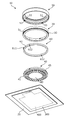
- FIG. 1 is a perspective view showing a schematic configuration of an input device according to an embodiment.
- FIG. 2 is an exploded perspective view of the input device according to the embodiment.
- FIG. 3 is an exploded perspective view of the input device according to the embodiment as viewed from a direction different from that of FIG.
- FIG. 4 is a cross-sectional view of the input device according to the embodiment.
- FIG. 5 is an enlarged cross-sectional view showing a part of the input device according to the embodiment.
- FIG. 6 is a plan view showing the first electrode and the second electrode according to the embodiment.
- FIG. 7 is a schematic view of the positional relationship between the first electrode and the second electrode according to the embodiment as viewed from the side.
- FIG. 8 is a block diagram showing a control configuration of the input device according to the embodiment.
- FIG. 9 is an explanatory diagram for explaining the detection of the movement amount of the input device according to the embodiment.
- FIG. 10 is an explanatory diagram schematically showing a layout example of the first electrode according to the present disclosure.
- FIG. 11 is a plan view showing the first electrode and the second electrode according to the first modification.
- FIG. 12 is a plan view showing the first electrode and the second electrode according to the second modification.
- FIG. 13 is a plan view showing the first electrode and the second electrode according to the modified example 3.
- FIG. 14 is a plan view showing the first electrode and the second electrode according to the modified example 4.
- FIG. 15 is an explanatory diagram for explaining the detection of the movement amount of the input device according to the modified example 4.
- FIG. 16 is a plan view showing the first electrode and the second electrode according to the modified example 5.
- FIG. 17 is a plan view showing the first electrode and the second electrode according to the modified example 6.
- the input device is in a state where a first electrode having one or more reference potential electrodes and two or more sets of transmitting electrodes and receiving electrodes is opposed to the first electrode at a predetermined interval.
- a second electrode that approaches or moves away from two or more sets of transmitting and receiving electrodes by rotating or moving, and one or more reference potential electrodes are two or more sets of transmitting or receiving electrodes.
- the second electrode approaching at least one set of transmitting and receiving electrodes among the electrodes, the second electrode faces at least a part of the second electrode, and two or more sets of transmitting and receiving electrodes are placed in the first region.
- It includes a first set of transmit and receive electrodes arranged and a second set of transmit and receive electrodes arranged in the second region, with the first set of transmit and receive electrodes relative to the second electrode.
- the phase when approaching or moving away is different from the phase when the second set of transmitting and receiving electrodes approach or move away from the second electrode.
- the second electrode approaches or is far from two or more sets of the transmitting electrode and the receiving electrode by rotating or moving in a state of facing the first electrode at a predetermined interval.
- Retreat. Therefore, during rotation or movement, the electrical state between the first electrode and the second electrode changes.
- the relative movement amount between the first electrode and the second electrode even without the third electrode. Since the first electrode and the second electrode face each other with a predetermined interval even during relative movement, friction does not occur. Therefore, damage to the first electrode and the second electrode can be suppressed, and the quality can be maintained for a long period of time.
- the phase is different from the change in the electric state caused by the first set arranged in the first region and the change in the electric state caused by the second set arranged in the second region. By detecting this phase difference, it is possible to detect the direction of rotation or movement.
- the reference potential electrode is a ground electrode.
- the reference potential electrode is the ground electrode, it is not necessary to add a power supply, and the circuit configuration can be simplified.
- the operating origin of the input device is a state in which the area where the first set of transmitting electrodes and the receiving electrodes overlap with the second electrode is equal to the area where the second set of transmitting electrodes and receiving electrodes overlap with the second electrode. (First state).
- the operating origin of the input device is substantially the distance that the first set of transmitting electrodes and the receiving electrodes are separated from the second electrode and the distance that the second set of transmitting electrodes and receiving electrodes are separated from the second electrode. It is a state that becomes even (second state).
- the operating origin of the input device is the first state or the second state
- the change in the electrical state caused by the first set arranged in the first region and the change in the electrical state are arranged in the second region.
- the origin of operation is near the intersection with the change in electrical state caused by the second set.
- the change in the electrical state caused by the first set and the change in the electrical state caused by the second set are on the positive side or the negative side with respect to a predetermined threshold value, respectively. Occurs on the same side.
- One change in the electrical state is distinguished into an ON signal and an OFF signal with reference to a predetermined threshold value. Then, the amount of movement is detected by combining the distinction results for the above two changes in the electrical state.
- the area of the first area and the area of the second area are substantially the same.
- the change in the electrical state caused by the first set and the change in the electrical state caused by the second set can be made equal, and the phase difference between the changes in the electrical state can be further increased. It can be detected reliably. Therefore, the quality of the input device can be improved without using the third electrode.
- two or more sets of transmitting electrodes and receiving electrodes have a comb-teeth shape.
- the transmitting electrode and the receiving electrode have a comb-shaped shape
- the space between the transmitting electrode and the receiving electrode is widened to increase the sensitivity, and the area is made larger than that in the case of the rod shape to secure the capacity. Can be done.
- At least two sets of the transmitting electrode and the receiving electrode are arranged side by side along the ring, and one or more reference potential electrodes are the first reference potential electrode arranged inside the ring and the above-mentioned reference potential electrode. It has a second reference potential electrode arranged on the outer side of the ring.
- the reference potential electrode has the first reference potential electrode and the second reference potential electrode, the electrical coupling of the reference potential can be strengthened, and the change in the electrical state of the first electrode can be made. Can be increased. If the change in the electrical state of the first electrode can be made large, the detection accuracy can be improved.
- the first electrode and the second electrode are transparent electrodes.
- the first electrode and the second electrode are transparent electrodes, the information on the back side of the input device can be transmitted through the first electrode and the second electrode. Therefore, it is possible to realize an input device with high design.
- the first electrode is the electrode of the touch sensor.
- the electrode of the touch sensor is used as the first electrode, when the input device is installed on the touch sensor, the electrode of the touch sensor and the first electrode of the input device can be used together. Therefore, it is possible to reduce the number of parts.
- the input device further includes an electrical shielding layer arranged on the opposite side of the second electrode in the first electrode.
- the electrical shielding layer is arranged on the side of the first electrode opposite to the second electrode, noise from the electrical equipment arranged on the back side of the input device can be blocked by the shielding layer. .. Therefore, it is possible to more accurately detect the relative movement amount between the first electrode and the second electrode.
- the input device further includes a transparent support, a transparent moving body, and an image display unit that irradiates at least one of the support and the moving body with light, and the support is an image display unit. Arranged on top, at least one of the support and the moving body directs the emitted light.
- the image display unit irradiates at least one of the support and the moving body with light and guides the light to at least one of the support and the moving body, it is optical with respect to the input device. You can give a production.
- the reference potential electrode does not have to face a part of the second electrode when the second electrode does not approach at least one set of the transmitting electrode and the receiving electrode.
- the reference potential electrode may face a part of the second electrode even when the second electrode does not approach at least one set of the transmitting electrode and the receiving electrode.
- the area of the portion of the reference potential electrode facing the second electrode may increase.
- FIG. 1 is a perspective view showing a schematic configuration of an input device 10 according to an embodiment.
- FIG. 2 is an exploded perspective view of the input device 10 according to the embodiment.
- FIG. 3 is an exploded perspective view of the input device 10 according to the embodiment as viewed from a direction different from that of FIG.
- FIG. 4 is a cross-sectional view of the input device 10 according to the embodiment.
- FIG. 4 is a cross-sectional view of the cut surface including the IV-IV line in FIG.
- the operating body 50 side is described as upward and the touch sensor 200 side is described as downward, but this is merely an example, and the above-described position may be used depending on the installation mode (posture) of the input device 10. It may not be a relationship.
- the input device 10 is installed on the touch sensor 200, and is a device that detects the amount of rotational movement by rotating the touch sensor 200.
- the input device 10 has a support 20, a fixed body 30, a moving body 40, an operating body 50, an urging portion 60, a first electrode 70, and a second electrode 80. ing.
- the support 20 is a substrate made of a translucent resin.
- the support 20 is shared with the substrate of the touch sensor 200. Therefore, an electrode pattern for multipoint detection (not shown) and a first electrode 70 for the input device 10 are formed on at least one of the pair of main surfaces of the support 20 to support the support.
- the electrode pattern and the first electrode 70 are transparent electrodes made of, for example, ITO.
- the first electrode 70 is the electrode of the touch sensor 200.
- the main surface of the support 20 is covered with a cover lens 21 made of a translucent member such as glass.
- the second electrode 80 is arranged at a position facing the first electrode 70 with the cover lens 21 interposed therebetween.
- a translucent adhesive layer (not shown) is interposed between the layers, and each member is adhered by the adhesive layer.
- a display panel 300 as an image display unit for displaying an image is arranged.
- the display panel 300 is a liquid crystal panel, an organic EL panel, or the like.
- An electrical shielding layer 400 is arranged between the display panel 300 and the touch sensor 200. That is, it can be said that the shielding layer 400 is arranged on the opposite side of the first electrode 70 from the second electrode 80.
- the shielding layer 400 can shield electrical noise from the display panel 300 arranged on the back side of the input device 10. Therefore, the shielding layer 400 may be arranged at least in a region overlapping the entire first electrode 70. However, if the shielding layer 400 is arranged in a wider range than the first electrode 70, it is possible to exert a higher noise reduction effect.
- the shielding layer 400 is a transparent electrode made of, for example, ITO.
- the fixed body 30 is a member fixed on the main surface of the support body 20.
- the fixed body 30 is formed in a cylindrical shape by, for example, a translucent resin.
- a pair of notches 31 are formed at positions facing each other at the upper end portion of the fixed body 30.
- An annular convex portion 32 continuous over the entire circumference is formed in the lower portion of the outer peripheral surface of the fixed body 30.
- the moving body 40 is a member that rotates with respect to the fixed body 30.
- the moving body 40 is formed in a bottomed cylindrical shape by, for example, a translucent resin.
- the moving body 40 is arranged so as to be concentric with the fixed body 30. That is, the center of rotation of the moving body 40 and the center of the fixed body 30 are arranged coaxially.
- a pair of notches 45 are formed at positions facing each other with the rotation center in between.
- a collar portion 41 protruding outward is provided over the entire circumference.
- An uneven structure 42 is formed on the upper surface of the collar portion 41.
- a plurality of concave portions 43 recessed in a direction orthogonal to the moving direction (rotational direction) of the moving body 40 and a plurality of convex portions 44 protruding in the direction are arranged alternately and continuously along the moving direction. ing.
- the concave portion 43 is recessed downward in a concave curved surface shape, and the convex portion 44 is projected upward in a convex curved surface shape.
- the upper surface of the concave-convex structure 42 that is, the upper surface of the flange portion 41 has a smoothly wavy shape.
- a second electrode 80 is attached to the lower surface of the moving body 40.
- the second electrode 80 is a transparent electrode made of, for example, ITO.
- a cover lens 21 is interposed between the second electrode 80 and the first electrode 70, and the second electrode 80 and the first electrode 70 are in a state of facing each other with a predetermined interval. That is, the moving body 40 holds the second electrode 80 in a state of facing the first electrode 70 at a predetermined interval.
- the moving body 40 rotates in conjunction with the operation of the operating body 50 by the user, and even during this rotational movement, the second electrode 80 and the first electrode 70 face each other with a predetermined interval. It is in a state. Due to the rotational movement of the moving body 40, a part of the second electrode 80 repeatedly approaches or moves away from the first electrode 70 in the moving direction.
- the operating body 50 is a member that is held so as to be relatively movable with respect to the fixed body 30 in a state of being engaged with the moving body 40.
- the operating body 50 is a member that rotates the moving body 40 when operated by the user.
- the operating body 50 is formed in a cylindrical shape by, for example, a translucent resin.
- the operating body 50 is arranged so as to be concentric with the moving body 40. That is, the center of rotation of the operating body 50, the center of rotation of the moving body 40, and the center of rotation of the moving body 40 are arranged coaxially.
- An annular top plate 51 extending inward over the entire circumference is formed at the upper end of the operating body 50.
- FIG. 5 is an enlarged cross-sectional view showing a part of the input device 10 according to the embodiment.
- the top plate portion 51 is a lid portion that closes the space between the fixed body 30 and the moving body 40.
- the inner peripheral surface of the top plate portion 51 is arranged flush with respect to the inner peripheral surface of the moving body 40.
- the lower surface of the top plate portion 51 has a stepped shape such that the inner peripheral portion 511 is above the outer peripheral portion 512.
- the outer peripheral portion 512 of the top plate portion 51 is in contact with the upper surface of the fixed body 30, which restricts the downward movement of the operating body 50.
- the inner peripheral portion 511 of the top plate portion 51 is separated from the upper surface of the moving body 40. As a result, the axial force is not applied from the operating body 50 to the moving body 40.
- a plurality of claw portions 53 that engage with the annular convex portion 32 of the fixed body 30 are arranged at predetermined intervals in the circumferential direction.
- the claw portion 53 is a portion protruding inward from the inner peripheral surface of the top plate portion 51.
- the claw portion 53 is arranged below the annular convex portion 32 so as to overlap the annular convex portion 32 of the fixed body 30 in the axial direction. Even if the operating body 50 rises and is about to be separated from the fixed body 30, the claw portion 53 is locked by abutting on the annular convex portion 32. That is, the structure is such that the operating body 50 does not come off from the fixed body 30.
- the operating body 50 is held so as to be relatively movable with respect to the fixed body 30. Since the lower surface of the claw portion 53 is an inclined surface that inclines outward as it goes downward, when the operating body 50 is assembled to the fixed body 30, the inclined surface is guided by the annular convex portion 32. The operating body 50 is smoothly elastically deformed. When the claw portion 53 passes through the annular convex portion 32, the operating body 50 returns to its original shape.
- a pair of convex pieces 52 projecting downward are arranged at positions facing each other.
- the convex piece 52 is fitted in the notch 45 of the moving body 40.
- the notch 45 of the moving body 40 is a portion to which an acting force is applied from the operating body 50 when the operating body 50 moves.
- the urging portion 60 is a portion that is arranged between the moving body 40 and the fixed body 30 and imparts urging force to the support 20 side to the moving body 40. is there.
- the urging portion 60 is arranged at a position different from that of the notch 45.
- the urging portion 60 has a holding body 61, an elastic body 62, and a sphere 63.
- the holding body 61 is a member that is fixed to the fixed body 30 and variably holds the elastic body 62 and the sphere 63.
- the holding body 61 is, for example, a member formed in a circular shape by a translucent resin.
- the holding body 61 is arranged so as to be concentric with the moving body 40. That is, the center of the holding body 61 and the center of rotation of the moving body 40 are arranged coaxially.
- a pair of protrusions 611 fitted to each notch 31 of the fixed body 30 are formed at positions facing each other with the rotation center interposed therebetween.
- the pair of protrusions 611 project outward from the outer peripheral surface of the holding body 61.
- the holding body 61 is fixed to the fixed body 30 by fitting the pair of protrusions 611 into each notch 31 of the fixed body 30.
- a pair of slits 612 whose lower surface is open is formed on the lower surface of the holding body 61.
- the pair of slits 612 are located at positions different from the pair of protrusions 611, and are arranged at positions facing each other with the center of rotation interposed therebetween.
- An elastic body 62 and a sphere 63 are housed in each slit 612. That is, a pair of elastic body 62 and sphere 63 is provided.
- Each slit 612 is arranged at a position overlapping the flange portion 41 of the moving body 40. That is, since each slit 612 overlaps the outer peripheral portion of the moving body 40, the elastic body 62 and the sphere 63 accommodated in each slit 612 also overlap the outer peripheral portion of the moving body 40.
- the upper portion of the slit 612 is formed in a truncated cone shape that tapers toward the top.
- An elastic body 62 is attached below the truncated cone-shaped portion.
- the portion of the slit 612 above the elastic body 62 is a relief portion 64 that receives elastic deformation when the elastic body 62 is pressed upward.
- the relief portion 64 is formed in the truncated cone shape described above, but in other words, it is formed in a concave shape that is recessed upward.
- the internal space of the relief portion 64 is a space for the elastic body 62 to escape. Due to such a space, elastic deformation of the elastic body 62 is promoted, and the elastic body 62 can be smoothly elastically deformed and elastically restored.
- the relief portion 64 has a tapered shape, it is possible to secure the wall thickness around the relief portion 64 while undergoing elastic deformation of the elastic body 62. Thereby, it is possible to suppress the vulnerability of the holding body 61 due to the slit 612.
- the elastic body 62 is an example of a pressing body that elastically deforms the elastic body 62 in conjunction with the movement of the moving body 40.
- the sphere 63 is, for example, a plate formed of a translucent resin.
- the elastic body 62 is a member having lower rigidity than other members (support 20, fixed body 30, moving body 40, operating body 50, holding body 61, and sphere 63).
- the elastic body 62 is formed of a translucent silicone resin.
- the elastic body 62 may be formed of a translucent material having elasticity, or may be formed in a shape exhibiting elasticity by using a translucent material.
- a sphere 63 is rotatably arranged below the elastic body 62.
- the sphere 63 is, for example, a sphere formed of a translucent resin.
- the sphere 63 is placed on the upper surface of the concave-convex structure 42 in the moving body 40.
- the sphere 63, the elastic body 62, and the holding body 61 are arranged upward in this order on the uneven structure 42. Since they are arranged in this order, the urging force toward the support 20 caused by the elastic body 62 can be applied to the moving body 40 via the sphere 63 and the concave-convex structure 42.
- the moving body 40 rotates with respect to the fixed body 30 and the holding body 61
- the concave portions 43 and the convex portions 44 of the concave-convex structure 42 pass alternately under the sphere 63. Therefore, the sphere 63 fluctuates up and down.
- the sphere 63 is lowered and does not push up the elastic body 62.
- the elastic body 62 retains its original shape.
- the sphere 63 gradually rises following the wavy shape of the upper surface of the concave-convex structure 42.
- the elastic body 62 is elastically deformed.
- the elastic body 62 tries to elastically return, so that the restoring force (urging force) acts on the sphere 63.
- the sphere 63 pushes down the uneven structure 42. That is, the moving body 40 is given an urging force from the urging portion 60 to the support 20 side.
- the alternate long and short dash line portion in FIG. 5 shows the sphere 63 and the elastic body 62 when the sphere 63 is placed on the apex of the convex portion 44.
- the elastic body 62 is in the most elastically deformed state, and the moving body 40 receives the largest urging force from the urging portion 60. Due to the rotation of the moving body 40, the urging force increases from the apex of the concave portion 43 to the apex of the convex portion 44 passing through the sphere 63.
- the urging force decreases from the apex of the convex portion 44 to the apex of the concave portion 43 passing through the sphere 63. That is, when the apex of the convex portion 44 passes through the sphere 63, the urging force changes from increasing to decreasing, and this switching is transmitted to the user via the operating body 50 as a click feeling.
- the urging force applied to the moving body 40 by the urging unit 60 is caused by the elastic body 62 and the sphere 63 in each slit 612. That is, the urging unit 60 applies an urging force to the moving body 40 from each of a pair of positions overlapping the outer peripheral portion of the moving body 40 at a position sandwiching the rotation center of the moving body 40. Therefore, the urging force can be applied to the moving body 40 in a well-balanced manner.
- the sphere 63 may push up the elastic body 62. In this case, the sphere 63 always receives the urging force from the elastic body 62. That is, the moving body 40 is always subjected to the urging force from the urging portion 60 to the support 20 side.
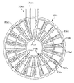
- FIG. 6 is a plan view showing the first electrode 70 and the second electrode 80 according to the embodiment.
- the first electrode 70 is provided with dot hatching, and the outer shape of the second electrode 80 is indicated by a broken line.
- the first electrode 70 is provided on the main surface of the support 20, and the second electrode 80 is provided on the lower surface of the moving body 40.
- the first electrode 70 and the second electrode 80 are in a state of facing each other with a predetermined interval via the cover lens 21.
- the first electrode 70 has a ground electrode 71 and at least two sets of a transmitting electrode 72 and a receiving electrode 73.
- the ground electrode 71 is an example of a reference potential electrode, and has a first ground electrode 74 (first reference potential electrode) and a second ground electrode 75 (second reference potential electrode).
- the reference potential electrode may be an electrode having a reference potential other than the ground potential.
- the first ground electrode 74 is formed in a substantially circular shape.
- the second ground electrode 75 is formed so as to surround the first ground electrode 74 at a predetermined interval.
- the region R between the first ground electrode 74 and the second ground electrode 75 is formed in a substantially annular shape. This region R is divided into a first region R1 and a second region R2.
- the first region R1 is a region on the left side of the region R
- the second region R2 is a region on the right side of the region R.
- the first region R1 and the second region R2 have the same area.
- a part of the ground electrode 71 is arranged at the boundary portion between the first region R1 and the second region R2.
- a part of the second ground electrode 75 is arranged at the upper boundary portion in FIG. In FIG. 6, a part of the first ground electrode 74 is arranged at the lower boundary portion.
- a plurality of sets of transmission electrodes 72 and reception electrodes 73 are arranged.
- the transmission conductive pattern 77 forming each set of transmission electrodes 72 is arranged along the outer circumference of the first ground electrode 74 in the region R.
- a plurality of transmission electrodes 72 are arranged radially along the circumferential direction.
- Each transmission electrode 72 is formed in a rod shape extending outward.
- the transmission electrode 72 arranged in the first region R1 is referred to as the first transmission electrode 721
- the transmission electrode 72 arranged in the second region R2 is referred to as the second transmission electrode 722.
- the plurality of first transmission electrodes 721 are arranged at regular intervals H in the circumferential direction.
- the plurality of second transmitting electrodes 722 are also arranged at regular intervals H in the circumferential direction, but the second transmitting electrode 722 is out of phase with the first transmitting electrode 721.
- the plurality of first transmission electrodes 721 are arranged at equal intervals in the circumferential direction starting from a position shifted to the left by an angle ⁇ with respect to the upper boundary portion.
- the plurality of second transmission electrodes 722 are arranged at equal intervals in the circumferential direction with respect to the upper boundary portion in the right direction and starting from a position deviated by an angle ⁇ larger than the angle ⁇ .
- a pair of receiving conductive patterns 781 and 782 forming each set of receiving electrodes 73 are arranged along the inner circumference of the second ground electrode 75 in the region R.
- the pair of receive conductive patterns 781 and 782 one of the received conductive patterns 781 is arranged in the first region R1, and the other received conductive pattern 782 is arranged in the second region R2.
- a plurality of receiving electrodes 73 are arranged radially along the circumferential direction. Each receiving electrode 73 is formed in a rod shape extending inward.
- the receiving electrode 73 arranged in the first region R1 is referred to as the first receiving electrode 731
- the receiving electrode 73 arranged in the second region R2 is referred to as the second receiving electrode 732.
- 14 sets of the first transmitting electrode 721 and the first receiving electrode 731 are provided in the first region R1
- 14 sets of the second transmitting electrode 722 and the second receiving electrode 732 are provided in the second region R2.
- Each first receiving electrode 731 faces a pair of first transmitting electrodes 721 at regular intervals W in the circumferential direction.
- Each second receiving electrode 732 faces the paired second transmitting electrode 722 at a constant interval W in the circumferential direction.
- the first receiving electrode 731 and the second receiving electrode 732 also have different phases.
- the case where the transmitting electrode 72 is arranged inside and the receiving electrode 73 is arranged outside is illustrated, but the positional relationship between the transmitting electrode and the receiving electrode may be reversed.
- the second electrode 80 has a circular portion 81, an outer ring portion 82, and a plurality of connecting portions 83.
- the circular portion 81 is a circular portion and substantially overlaps with the first ground electrode 74 in a plan view.
- the outer ring portion 82 is a portion concentric with the circular portion 81 that surrounds the circular portion 81 over the entire circumference at a predetermined interval.
- the outer ring portion 82 substantially overlaps with the second ground electrode 75 in a plan view.
- 32 of the plurality of connecting portions 83 are provided in the present embodiment.
- the plurality of connecting portions 83 are arranged between the circular portion 81 and the outer ring portion 82, and are arranged at equal intervals along the circumferential direction. Specifically, the connecting portions 83 are arranged at intervals H in the circumferential direction.
- Each connecting portion 83 has a rod shape along the radial direction, and is connected to the circular portion 81 and the outer ring portion 82.
- the second electrode 80 rotates as the moving body 40 rotates. At this time, the second electrode 80 rotates with a predetermined distance from the first electrode 70.
- each connecting portion 83 repeatedly approaches or retreats from each transmitting electrode 72 and receiving electrode 73 in the circumferential direction.
- each connecting portion 83 arranged in the first region R1 has a uniform positional relationship with respect to each pair of the first transmitting electrode 721 and the first receiving electrode 731.
- Each connecting portion 83 arranged in the second region R2 has a uniform positional relationship with respect to each set of the second transmitting electrode 722 and the second receiving electrode 732.
- the phases of the first transmitting electrode 721 and the first receiving electrode 731 and the second transmitting electrode 722 and the second receiving electrode 732 are different from each other. Therefore, the phases of the connecting portions 83 when approaching or moving away from them are also different.
- FIG. 7 is a schematic view of the positional relationship between the first electrode 70 and the second electrode 80 according to the embodiment as viewed from the side.
- a set of the first transmitting electrode 721 and the first receiving electrode 731 of the first electrode 70 are collectively illustrated, and a set of the second transmitting electrode 722 and the second receiving electrode 732 are collectively illustrated. ing.
- the first state includes the area where the first transmitting electrode 721 and the first receiving electrode 731 overlap with the connecting portion 83 of the second electrode 80 (superimposed area S1), and the second transmitting electrode 722 and the second receiving electrode 732. Is a state in which the area overlapped with the connecting portion 83 (superimposed area S2) is equal.
- the transmitting electrode 72 and the receiving electrode 73 of each set are arranged apart from each other in the circumferential direction, but the region between them is also a region forming the transmitting electrode 72 and the receiving electrode 73. Therefore, when the region also overlaps with the connecting portion 83, it is included in the overlapping areas S1 and S2.
- (B) in FIG. 7 shows the second state.
- the second state is a distance L1 in which the first transmitting electrode 721 and the first receiving electrode 731 are separated from the connecting portion 83, and a distance L2 in which the second transmitting electrode 722 and the second receiving electrode 732 are separated from the connecting portion 83. It is a state of equalization.
- "equal" is not only completely the same, but also includes those containing a slight difference of about several percent. That is, it may be substantially equal. This is the same even if it is equivalent.
- the second electrode 80 rotates relative to the first electrode 70. Therefore, the transition from the first state to the second state and the transition from the second state to the first state are repeatedly performed. Further, during rotation, the circular portion 81 of the second electrode 80 always faces the first ground electrode 74, and the outer ring portion 82 of the second electrode 80 also faces the second ground electrode 75. Always facing each other. Therefore, even while the second electrode 80 is rotating, the electrical coupling between the circular portion 81 and the first ground electrode 74 becomes strong, and the electrical coupling between the outer ring portion 82 and the second ground electrode 75 becomes stronger.
- the electric capacity between the transmitting electrode 72 and the receiving electrode 73 and the connecting portion 83 becomes smaller when the superposed area is the largest. On the contrary, when the transmitting electrode 72 and the receiving electrode 73 and the connecting portion 83 are farthest apart, the electric capacity becomes large. From each receiving electrode 73, the amount of change in the electric capacity at that time is output as an electric signal.
- FIG. 8 is a block diagram showing a control configuration of the input device 10 according to the embodiment.
- the input device 10 includes a first electrode 70, a touch sensor 200, and a control unit 90 electrically connected to the display panel 300.
- the control unit 90 includes a CPU, a RAM, and a ROM, and the CPU expands a program stored in the ROM into the RAM and executes the program to execute various processes.
- the control unit 90 applies electric power to the transmitting electrode 72 of the first electrode 70, and detects the relative movement amount of the second electrode 80 with respect to the first electrode 70 based on the electric signal received from the receiving electrode 73. To do. The detection of the movement amount will be described later.
- the control unit 90 also receives the input signal from the touch sensor 200, and controls the display content of the display panel 300 based on the input signal and the detected movement amount.
- the control unit 90 controls the emission color of the pixel group overlapping the support 20 on the display panel 300.
- the display panel 300 irradiates the support 20 with light.
- each member of the input device 10 support 20, fixed body 30, moving body 40, operating body 50, urging portion 60, first electrode 70, and second electrode 80
- the light emitted from the display panel 300 guides each member. Therefore, the light from the display panel 300 can give an optical effect to each member.
- FIG. 9 is an explanatory diagram for explaining the detection of the movement amount of the input device 10 according to the embodiment.
- FIG. 9A shows a change in capacitance between the first electrode 70 and the second electrode 80 during rotation.
- the capacitance change formed by the first transmitting electrode 721 and the first receiving electrode 731 and the connecting portion 83 is defined as the first capacitance change Q1, and the second transmitting electrode 722, the second receiving electrode 732, and the connecting portion 83 are connected to each other.
- the capacity change to be made is referred to as the second capacity change Q2.
- the first capacitance change Q1 and the second capacitance change Q2 have waveforms having different phases from each other.
- the overlapping area between the first transmitting electrode 721 and the first receiving electrode 731 and the connecting portion 83 is the largest, and at the point P12, the first transmitting electrode 721 and the first receiving electrode The distance between the 731 and the connecting portion 83 is the largest.
- the overlapping area between the second transmitting electrode 722 and the second receiving electrode 732 and the connecting portion 83 is the largest, and at the point P22, the second transmitting electrode 722 and the second transmitting electrode 722 and the second (Ii) The distance between the receiving electrode 732 and the connecting portion 83 is the largest.
- the point P10 is set as the mechanical operation origin of the input device 10.
- the point P10 is a location corresponding to the second state, and is near the intersection of the first capacitance change Q1 and the second capacitance change Q2.
- at point P10 at least one of the first capacitance change Q1 and the second capacitance change Q2 may be calibrated so that the first capacitance change Q1 and the second capacitance change Q2 intersect.
- FIG. 9 shows the change in the electrical state during rotation.
- the electrical state is the amount of change of the first capacitance change Q1 and the second capacitance change Q2, respectively.
- This amount of change is detected as an electric signal in the control unit 90.
- the waveform of the capacitance change rate ( ⁇ c / c) of the first capacitance change Q1 is the first waveform W1
- the waveform of the capacitance change rate of the second capacitance change Q2 is the second waveform W2.
- the control unit 90 distinguishes a portion of each of the first waveform W1 and the second waveform W2 as an ON signal and a portion below a predetermined threshold value as an OFF signal.
- FIG. 9 (c) the distinction result T1 for the first waveform W1 and the distinction result T2 for the second waveform W2 are shown.
- each of the first waveform W1 and the second waveform W2 is generated on the negative side with respect to a predetermined threshold value, so that the distinction results T1 and T2 are also OFF signals at the operating origin. It is common in. If the point P19 is set as the operating origin, the ON signal and the OFF signal are mixed at the operating origin, which is not preferable.
- the control unit 90 sets the portion where each of the first waveform W1 and the second waveform W2 becomes an ON signal as the movement amount per unit.
- the movement amount per unit is the movement amount for one click.
- control unit 90 determines that the case where the first waveform W1 outputs the ON signal first and the second waveform W2 outputs the ON signal later within the movement amount per unit is "normal rotation". The case where the second waveform W2 outputs the ON signal first and the first waveform W1 outputs the ON signal later is determined to be "reversal".
- the control unit 90 may invert the first waveform and the second waveform according to their respective positive and negative values to distinguish between an ON signal and an OFF signal.
- the input device 10 has a first electrode 70 having one or more ground electrodes 71, two or more sets of transmission electrodes 72 and a receiving electrode 73, and the first electrode 70.
- a second electrode 80 that approaches or moves away from two or more sets of transmitting electrodes 72 and receiving electrodes 73 by rotating in a state of facing each other at a predetermined interval is provided, and at least.
- one ground electrode 71 is at least the second electrode 80.
- Two or more sets of the transmitting electrode 72 and the receiving electrode 73 facing a part thereof are the first set of the transmitting electrode 72 and the receiving electrode 73 arranged in the first region R1 and the second set arranged in the second region R2.
- the phase when the first set of the first transmitting electrode 721 and the first receiving electrode 731 approaches or moves away from the second electrode 80 including the set of the transmitting electrode 72 and the receiving electrode 73 is the second set of the second transmitting.
- the phases of the electrode 722 and the second receiving electrode 732 are different from those when approaching or moving away from the second electrode 80.
- the second electrode 80 moves with respect to at least two sets of the transmitting electrode 72 and the receiving electrode 73 by rotating in a state of facing the first electrode 70 at a predetermined interval. Approach or move away in the direction. Therefore, during rotation, the electrical state between the first electrode 70 and the second electrode 80 changes. By detecting this change in the electrical state, it is possible to detect the relative movement amount between the first electrode 70 and the second electrode 80 even without the third electrode. Since the first electrode 70 and the second electrode 80 face each other with a predetermined interval even during relative movement, friction does not occur. Therefore, damage to the first electrode 70 and the second electrode 80 can be suppressed, and the quality can be maintained for a long period of time.
- the phases when approaching or moving away from the second electrode 80 are different. Therefore, the phase is different from the change in the electric state caused by the first set and the change in the electric state caused by the second set. By detecting this phase difference, it is possible to detect the direction of rotation as well.
- the reference potential electrode is the ground electrode 71.
- the reference potential electrode is the ground electrode 71, it is not necessary to add a power supply, and the circuit configuration can be simplified.
- the operating origin of the input device 10 is such that the overlapping area S1 on which the first set of the first transmitting electrode 721 and the first receiving electrode 731 overlap the second electrode 80 is the second set of the second transmitting electrode 722 and the second. This is a state (first state) in which the receiving electrode 732 is substantially equal to the superposed area S2 superimposed on the second electrode 80.
- the operating origin of the input device 10 is such that the distance L1 at which the first set of the first transmitting electrode 721 and the first receiving electrode 731 are separated from the second electrode 80 is the second set of the second transmitting electrode 722 and the second.
- the operating origin of the input device 10 is the first state or the second state
- the change in the electrical state caused by the set arranged in the first region R1 and the change in the electrical state are arranged in the second region R2.
- the origin of operation is near the intersection with the change in electrical state caused by the set.
- the change in the electrical state caused by the set arranged in the first region R1 and the change in the electrical state caused by the set arranged in the second region R2 are generated. Since it occurs on the same side of the positive side or the negative side with respect to a predetermined threshold value, these distinction results are also shared between the ON signal and the OFF signal at the operating origin. Thereby, it is possible to more accurately detect the relative movement amount between the first electrode 70 and the second electrode 80. Therefore, the quality of the input device 10 can be improved without using the third electrode.
- the area of the first region R1 and the area of the second region R2 are substantially the same.
- the change in the electrical state caused by the first set and the change in the electrical state caused by the second set can be made equal, and the phase difference between the changes in the electrical state can be further increased. It can be detected reliably. Therefore, the quality of the input device 10 can be improved without using the third electrode.
- At least two sets of the transmitting electrode 72 and the receiving electrode 73 are arranged side by side along the ring, and one or more ground electrodes 71 are arranged with the first ground electrode 74 arranged inside the ring. , A second ground electrode 75 arranged on the outer side of the ring.
- the ground electrode 71 has the first ground electrode 74 and the second ground electrode 75, the electrical coupling of the ground potential can be strengthened, and the electrical state of the first electrode 70 can be increased.
- the change can be large. If the change in the electrical state of the first electrode 70 can be made large, the detection accuracy can be improved.
- first electrode 70 and the second electrode 80 are transparent electrodes.
- the first electrode 70 and the second electrode 80 are transparent electrodes, the information on the back side of the input device 10 can be transmitted through the first electrode 70 and the second electrode 80. Therefore, it is possible to realize an input device 10 having a high design.
- the first electrode 70 is an electrode of the touch sensor 200.
- the electrode of the touch sensor 200 is used as the first electrode 70, when the input device 10 is installed on the touch sensor 200, the electrode of the touch sensor 200 and the first electrode 70 of the input device 10 are separated. Can also be used. Therefore, it is possible to reduce the number of parts.
- the input device 10 further includes an electrical shielding layer 400 arranged on the opposite side of the second electrode 80 in the first electrode 70.
- the electrical shielding layer 400 is arranged on the side of the first electrode 70 opposite to the second electrode 80, the noise from the electrical equipment arranged on the back side of the input device 10 is blocked by the shielding layer 400. Can be blocked with. Therefore, it is possible to more accurately detect the relative movement amount between the first electrode 70 and the second electrode 80.
- the input device 10 holds and supports the display panel 300 (image display unit), the translucent support 20 which is arranged on the display panel 300 and supports the first electrode 70, and the second electrode 80.
- a translucent moving body 40 that rotates and moves with respect to the body 20 is provided, and the display panel 300 irradiates at least one of the support 20 and the moving body 40 with light, and irradiates the light to the support 20 and the moving body 40. Guide light to at least one of the bodies 40.
- the display panel 300 irradiates at least one of the support 20 and the moving body 40 with light, and guides the light to at least one of the support 20 and the moving body 40.
- an optical effect can be applied.
- the input device 10 first sets the first electrode 70, the support 20 that supports the first electrode 70, the fixed body 30 fixed to the support 20, the second electrode 80, and the second electrode 80.
- the moving body 40 which moves the second electrode 80 closer to or further away from the first electrode 70 by holding and rotating the electrode 70 in a state of facing each other at a predetermined distance, is engaged with the moving body 40.
- An operating body 50 held in the fixed body so as to be relatively movable with respect to the fixed body 30 in the state, and the operating body 50 that rotates the moving body 40 by being operated by the user, and the moving body 40 and the fixed body. It has an urging portion 60, which is arranged between the 30 and 30 and applies an urging force toward the support 20 to the moving body 40.
- the urging unit 60 applies the urging force toward the support 20 to the moving body 40, the first electrode 70 supported by the support 20 is held by the moving body 40. It can be pressed toward the electrode 80. As a result, even when the moving body 40 is moving, the second electrode 80 is pressed against the first electrode 70, and the distance between them is kept constant. Therefore, the change in the electrical state between the first electrode 70 and the second electrode 80 can be reliably detected. Therefore, the sensitivity of changes in the electrical state of the input device 10 can be maintained.
- the moving body 40 is independently given the acting force given by the operating body 50 and the urging force given by the urging unit 60 at the time of movement.
- the acting force given by the operating body 50 and the urging force given by the urging unit 60 at the time of movement are independently applied to the moving body 40, the acting force and the urging force can be obtained. It can act on different locations on the moving body 40. Therefore, the moving body 40 can be moved smoothly. Since the moving body 40 moves smoothly, friction with respect to the first electrode 70 and the second electrode 80 can also be suppressed.
- a plurality of recesses 43 and a plurality of convex portions 44 projecting in the direction orthogonal to the moving direction of the moving body 40 are continuously and alternately arranged along the moving direction.
- the concave-convex structure 42 is provided, and the urging portion 60 is arranged between the elastic body 62 for applying the urging force and the concave-convex structure 42 and the elastic body 62, and is elastic in conjunction with the movement of the moving body 40. It has a sphere 63 that elastically deforms the body 62, and a holding body 61 that is fixed to the fixed body 30 and holds the elastic body 62 and the sphere 63 in a variable manner.
- the urging force received from the elastic body 62 increases from the apex of the concave portion 43 of the concave-convex structure 42 to the apex of the convex portion 44 passing through the sphere 63.
- the urging force received from the elastic body 62 decreases from the apex of the convex portion 44 to the apex of the concave portion 43 passing through the sphere 63. That is, when the apex of the convex portion 44 passes through the sphere 63, the urging force changes from an increase to a decrease, so that this switching can be transmitted to the user as a click feeling.
- the holding body 61 is formed with a concave relief portion 64 that receives elastic deformation of the elastic body 62, and the relief portion 64 is formed at a portion opposite to the sphere 63 with respect to the elastic body 62. ing.
- the holding body 61 is provided with a concave relief portion 64 that receives elastic deformation of the elastic body 62, the internal space of the relief portion 64 is a space for the elastic body 62 to escape. Therefore, elastic deformation of the elastic body 62 can be promoted, and even a thin elastic body 62 can be smoothly elastically deformed and elastically restored. Therefore, the elastic body 62 can be made thin.
- the pressing body that elastically deforms the elastic body 62 in conjunction with the movement of the moving body 40 is the sphere 63. According to this, since the pressing body is a sphere, the sphere 63 can be smoothly moved on the uneven structure 42, and smooth operability can be realized.
- the moving body 40 and the operating body 50 rotate around the center of rotation, and the urging portion 60 sandwiches the center of rotation of the moving body 40 and moves from a pair of positions overlapping the outer peripheral portion of the moving body 40. Gives urging power to 40.
- the pair of urging portions 60 are positioned to sandwich the rotation center of the moving body 40, and urging force is applied to the moving body 40 from the pair of positions overlapping the outer peripheral portion of the moving body 40. Therefore, it is possible to give a well-balanced urging force to the moving body 40. Therefore, the second electrode 80 can be stably pressed against the first electrode 70.
- the input device 10 first sets the first electrode 70, the support 20 that supports the first electrode 70, the fixed body 30 fixed to the support 20, the second electrode 80, and the second electrode 80.
- the second electrode 80 is engaged with the moving body 40 that approaches or moves away from the first electrode 70.
- the operating body 50 is held in the fixed body 30 so as to be relatively movable with respect to the fixed body 30 in the state, and is fixed to the moving body 40 and the operating body 50 that rotates the moving body 40 by being operated by the user.
- a urging portion 60 which is arranged between the body 30 and applies an urging force to the support 20 side to the moving body 40, and the moving body 40 is orthogonal to the moving direction of the moving body 40.
- a plurality of concave portions 43 recessed in the direction and convex portions 44 protruding in the direction have a concave-convex structure 42 in which a plurality of convex portions 44 are continuously arranged along the moving direction, and the urging portion 60 is for applying an urging force.
- a sphere 63 which is arranged between the elastic body 62 and the concave-convex structure 42 and the elastic body 62 and elastically deforms the elastic body 62 in conjunction with the movement of the moving body 40, and an elastic body 62 fixed to the fixed body 30.
- a holding body 61 that variably holds the sphere 63, the support 20, the fixed body 30, the moving body 40, the operating body 50, the elastic body 62, the sphere 63, and the holding body 61. Has translucency.
- the elastic body 62, the sphere 63, and the holding body 61 which are structures for giving a click feeling to the operating body 50, have translucency, a metal click spring is not used. However, it is possible to enhance the translucency inside the input device 10 while realizing a click feeling.
- the input device 10 since the support 20, fixed body 30, moving body 40, operating body 50, elastic body 62, sphere 63, and holding body 61 forming the input device 10 have translucency, the input device 10 as a whole is optically optical. Production is possible.
- the uneven structure 42 is arranged closer to the support 20 than the holding body 61, and the sphere 63 and the elastic body 62 are arranged in this order on the uneven structure 42.
- the urging force toward the support 20 caused by the elastic body 62 is applied to the sphere 63 and the concave-convex structure 42. It can be imparted to the moving body 40 via. Therefore, the urging force toward the support 20 can be reliably applied to the moving body 40.
- the sphere 63 moves up and down in conjunction with the moving uneven structure 42.
- the sphere 63 may be diffusely reflected by the ascending / descending motion to cause flicker.
- the elastic body 62 is arranged outside the sphere 63, the flicker caused by the sphere 63 is less noticeable. As a result, the optical effect can be enhanced.
- FIG. 10 is an explanatory diagram schematically showing a layout example of the first electrode according to the present disclosure.
- FIG. 10A shows a layout corresponding to the first electrode 70 according to the above embodiment, and the first region R1 and the second region R2 each have a semicircular arc shape. This layout is called the first layout.
- the first region R1b and the second region R2b of the first electrode 70B form concentric circles. This layout is called the second layout.
- the first region R1c and the second region R2c of the first electrode 70C each have a semicircular shape, and the first region R1c and the second region R2c are evenly 2 in the circumferential direction. It is divided.
- Each divided region of the first region R1c is designated as a first divided region c11 and a second divided region c12, and each divided region of the second region R2c is designated as a third divided region c23 and a fourth divided region c24.
- the first division region c11, the second division region c12, the third division region c23, and the fourth division region c24 each have a 1/4 arc shape. This layout is called the third layout.
- the first region R1d and the second region R2d of the first electrode 70D are concentric, respectively, and the first region R1d and the second region R2d are evenly divided into two in the circumferential direction.
- the divided regions of the first region R1d are designated as the first divided region d11 and the second divided region d12, and the divided regions of the second region R2d are designated as the third divided region d23 and the fourth divided region d24.
- the first division area d11, the second division area d12, the third division area d23, and the fourth division area d24 each have a semicircular shape.
- This layout is called the fourth layout.
- specific examples from the second layout to the fourth layout will be described.
- FIG. 11 is a plan view showing the first electrode 70A1 and the second electrode 80A1 according to the first modification.
- the outer shape of the second electrode 80A1 is shown by a broken line.
- the transmitting electrode 72 and the receiving electrode 73 of the first electrode 70 are formed in a rod shape.
- this modification 1 the case where the transmitting electrode 72a1 and the receiving electrode 73a1 of the first electrode 70A1 are formed in a comb-teeth shape is illustrated.
- the transmitting electrode 72a1 has a plurality of tooth portions 725a protruding toward the paired receiving electrode 73a1.
- the receiving electrode 73a1 has a plurality of tooth portions 735a protruding toward the paired transmitting electrode 72a1.
- the plurality of tooth portions 725a and the plurality of tooth portions 725a are alternately arranged along the radial direction in a separated state.
- the transmitting electrode 72a1 and the receiving electrode 73a1 have a comb tooth shape.
- the transmitting electrode 72a1 and the receiving electrode 73a1 have a comb-tooth shape, the space between the transmitting electrode 72a1 and the receiving electrode 73a1 is widened to increase the sensitivity, but the area is made larger than that in the rod shape to increase the capacitance. Can be secured.
- the ground electrode 71 always faces a part of the second electrode 80 is illustrated.
- the ground electrode 71a1 should face a part of the second electrode 80A1 when the second electrode 80A1 is close to at least one set of the transmitting electrode 72a1 and the receiving electrode 73a1. Just do it.
- the first ground electrode 74a1 of the ground electrode 71a1 includes an inner ring portion 741a and a plurality of extending portions 742a.
- the plurality of extending portions 742a extend radially from the outer peripheral edge of the inner ring portion 741a.
- the extending portions 742a are evenly arranged in the circumferential direction and are formed in a substantially fan shape.
- Each extension portion 742a is arranged at a position corresponding to the transmission electrode 72a1 and the reception electrode 73a1 of each set in the circumferential direction.
- the second electrode 80A1 includes an outer ring portion 82a1 and a plurality of connecting portions 83a1.
- the outer ring portion 82a1 is a portion formed in a substantially annular shape, and is provided so as to surround the first electrode 70A1 in a plan view.
- the plurality of connecting portions 83a1 are portions connected to the inner peripheral edge of the outer ring portion 82a1 and are arranged at equal intervals along the circumferential direction.
- the connecting portion 83a1 extends along the radial direction until the tip portion is arranged in the vicinity of the inner ring portion 741a of the first ground electrode 74a1.
- the same number of connecting portions 83a1 as the extending portions 742a are provided.
- the width of the connecting portion 83a1 in the circumferential direction is smaller than the width of the extending portion 742a.
- the width of the extension portion 742a in the circumferential direction is set to a width that overlaps the extension portion 742a when the connection portion 83a1 overlaps a part of the pair of the transmission electrode 72a1 and the reception electrode 73a1 in a plan view.
- the ground electrode 71a1 faces a part of the second electrode 80A1 when the connecting portion 83a1 of the second electrode 80A1 is close to at least one set of the transmitting electrode 72a1 and the receiving electrode 73a1 during rotational movement. It will be.
- FIG. 12 is a plan view showing the first electrode 70A2 and the second electrode 80A2 according to the second modification.
- the outer shape of the second electrode 80A2 is shown by a broken line.
- the case where the first ground electrode 74 of the first electrode 70 is formed in a substantially circular shape is illustrated.
- this modification 2 the case where the first ground electrode 74a2 of the first electrode 70A2 is formed in a substantially annular shape is illustrated.
- the second electrode 80A2 also forms the circular portion 81a2 in a substantially annular shape.
- the inner diameter of the first ground electrode 74a2 is smaller than the inner diameter of the circular portion 81a2.
- the second electrode 80A2 does not have an outer ring portion.
- FIG. 13 is a plan view showing the first electrode 70B and the second electrode 80B according to the third modification.
- the outer shape of the second electrode 80B is shown by a broken line.
- the first electrode 70B has a ground electrode 71b, and at least two sets of transmitting electrodes 72b and receiving electrodes 73b.
- the ground electrode 71b is formed in a substantially circular shape so as to surround each set of transmission electrode 72b and reception electrode 73b.
- the annular portion of the outer peripheral portion is the first region R1b
- the annular portion of the inner peripheral portion is the second region R2b.
- the transmission conductive pattern 77b forming each set of transmission electrodes 72b is arranged in the first region R1b and the second region R2b along the inner circumference of the ground electrode 71b.
- a plurality of transmission electrodes 72b are radially arranged along the circumferential direction.
- Each transmission electrode 72b is evenly arranged in the circumferential direction.
- Each transmission electrode 72b has a rod shape extending along the radial direction, and both ends thereof are refracted in the circumferential direction.
- the portion arranged in the first region R1b is the first transmission electrode 721b
- the portion arranged in the second region R2b is the second transmission electrode 722b.
- the pair of receiving conductive patterns 781b and 782b forming each set of receiving electrodes 73b are arranged along the inner circumference of the ground electrode 71b, respectively.
- one received conductive pattern 781b is arranged in the first region R1b
- the other received conductive pattern 782b is arranged in the second region R2b.
- a plurality of receiving electrodes 73b are arranged radially along the circumferential direction in one receiving conductive pattern 781b and the other receiving conductive pattern 782b.
- Each receiving electrode 73b is formed in a rod shape extending along the radial direction, and its tip portion is refracted in the circumferential direction.
- the receiving electrode 73b arranged in the first region R1b is referred to as the first receiving electrode 731b
- the receiving electrode 73b arranged in the second region R2b is referred to as the second receiving electrode 732b.
- the first receiving electrode 731b and each second receiving electrode 732b are arranged at the same position in the circumferential direction.
- the first receiving electrode 731b and each second receiving electrode 732b face the paired first transmitting electrode 721b and the second transmitting electrode 722b at regular intervals in the circumferential direction.
- the second electrode 80B includes an outer ring portion 82b and a plurality of connecting portions 83b.
- the outer ring portion 82b is a portion formed in a substantially annular shape, and substantially overlaps the ground electrode 71b in a plan view.
- the plurality of connecting portions 83b are portions connected to the inner peripheral edge of the outer ring portion 82b, and are arranged at equal intervals along the circumferential direction.
- the connecting portion 83b has a stepped shape so that the portion corresponding to the first region R1b and the portion corresponding to the second region R2b are displaced in the circumferential direction.
- the connecting portion 83b has a phase for each pair of the first transmitting electrode 721b and the first receiving electrode 731b, and a phase for each pair of the second transmitting electrode 722b and the second receiving electrode 732b. Will be different.
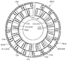
- FIG. 14 is a plan view showing the first electrode 70C1 and the second electrode 80C1 according to the modified example 4.
- the outer shape of the second electrode 80C1 is shown by a broken line.
- the second electrode 80C1 is different from the second electrode 80 according to the embodiment in that the number of connecting portions 83 installed is smaller.
- the number of connecting portions 83 installed is halved as compared with the second electrode 80 according to the embodiment.
- the number of connected portions 83 of the second electrode 80C1 is 16. Therefore, the distance between the connecting portions 83 of the second electrode 80C1 in the circumferential direction is wider than that of the second electrode 80 according to the embodiment.
- the first electrode 70C1 has a ground electrode 71c1 and at least two sets of transmitting electrodes 72c1 and receiving electrodes 73c1.
- the ground electrode 71c1 has a first ground electrode 74c1 and a second ground electrode 75c1.
- the first ground electrode 74c1 is formed in a substantially circular shape.
- the annular region surrounding the first ground electrode 74c1 is the region Rc.
- This region Rc is divided into a first region R1c and a second region R2c. Further, the first region R1c is evenly divided into two in the circumferential direction, and is divided into a first division region c11 and a second division region c12.
- the second region R2c is evenly divided into two in the circumferential direction, and is divided into a third division region c23 and a fourth division region c24.
- the second ground electrode 75c1 includes a plurality of divided ground electrodes.
- the plurality of divided ground electrodes are the first divided ground electrode 76c1, the second divided ground electrode 77c1, the third divided ground electrode 78c1, and the fourth divided ground electrode 79c1.
- the first division ground electrode 76c1 is partially extended so as to overlap the outer ring portion 82 of the second electrode 80C1 in a plan view, and the tip portion thereof is a boundary between the first division region c11 and the second division region c12. It is located in.
- the second divided ground electrode 77c1 is partially extended so as to overlap the outer ring portion 82 of the second electrode 80C1 in a plan view, and its tip portion is a boundary between the third divided region c23 and the fourth divided region c24. It is located in.
- a part of the third division ground electrode 78c1 is extended so as to overlap the outer ring portion 82 of the second electrode 80C1 in a plan view, and the tip portion thereof includes the first division region c11 and the third division region c23. It is placed on the border.
- the tip of the fourth division ground electrode 79c1 is arranged at the boundary between the second division region c12 and the fourth division region c24.
- a plurality of sets of transmission electrodes 72c1 and reception electrodes 73c1 are arranged in the region Rc.
- the transmission conductive pattern 77c forming each set of transmission electrodes 72c1 is arranged along the outer circumference of the first ground electrode 74c1 in the region Rc.
- a plurality of transmission electrodes 72c1 are radially arranged along the circumferential direction.
- Each transmission electrode 72c1 is formed in a rod shape extending outward.
- each set of receiving electrodes 73c1 are arranged outside the transmitting conductive pattern 77c in the region Rc.
- the reception conductive pattern 781c1 is provided with a plurality of reception electrodes 73c1 arranged in the first partition region c11.
- the reception conductive pattern 782c1 is provided with a plurality of reception electrodes 73c1 arranged in the second division region c12.
- the reception conductive pattern 783c1 is provided with a plurality of reception electrodes 73c1 arranged in the third division region c23.
- the reception conductive pattern 784c1 is provided with a plurality of reception electrodes 73c1 arranged in the fourth division region c24.
- each divided region three sets of transmitting electrodes 72c1 and three sets of receiving electrodes 73c1 are provided. As compared with the above embodiment, since the transmitting electrode 72c1 and the receiving electrode 73c1 are thinned out, the distance between the sets in the circumferential direction is widened. Further, in each divided region, a plurality of sets of transmitting electrodes 72c1 and receiving electrodes 73c1 are arranged so as to have different phases in the circumferential direction from a plurality of sets of transmitting electrodes 72c1 and receiving electrodes 73c1 in other divided regions. .. Therefore, a phase difference occurs in the capacitance change between the transmitting electrode 72c1 and the receiving electrode 73c1 and the connecting portion 83 of the second electrode 80C1 in each divided region during rotational movement.
- FIG. 15 is an explanatory diagram for explaining the detection of the movement amount of the input device according to the modified example 4.
- FIG. 15A shows the capacitance change between the first electrode 70C1 and the second electrode 80C1 during rotational movement.
- the capacitance change formed by the plurality of sets of transmission electrodes 72c1 and reception electrode 73c1 and the connecting portion 83 in the first partition region c11 is referred to as the first capacitance change Q11.
- the capacitance change between the plurality of sets of transmission electrodes 72c1 and reception electrode 73c1 and the connecting portion 83 in the second division region c12 is referred to as the second capacitance change Q12.
- the capacitance change between the plurality of sets of transmission electrodes 72c1 and reception electrode 73c1 and the connecting portion 83 in the third division region c23 is referred to as the third capacitance change Q13.
- the capacitance change between the plurality of sets of transmission electrodes 72c1 and reception electrode 73c1 and the connecting portion 83 in the fourth division region c24 is referred to as the fourth capacitance change Q14.
- points P20 and P30 are set as the mechanical operation origin of the input device 10.
- Points P20 and P30 are locations corresponding to the second state, are near the intersection of the first capacitance change Q11 and the third capacitance change Q13, and are the intersections of the second capacitance change Q12 and the fourth capacitance change 14. It is in the vicinity.
- FIG. 15 shows a change in the electrical state during rotational movement.
- the electrical state is the amount of change of each of the first capacitance change Q11 to the fourth capacitance change Q14.
- This amount of change is input to the control unit 90 as an electric signal.
- the waveform of the capacitance change rate of the first capacitance change Q11 is the first waveform W11
- the waveform of the capacitance change rate of the second capacitance change Q12 is the second waveform W12
- the waveform of the third capacitance change Q13 is the third waveform W13
- the waveform of the capacitance change rate of the fourth capacitance change Q14 is the fourth waveform W14.
- the control unit 90 distinguishes each of the first waveform W11 to the fourth waveform W14 as an ON signal for a portion above a predetermined threshold value and an OFF signal for a portion below the predetermined threshold value.
- the distinction result is shown in FIG. 15 (c).
- FIG. 15 (c) shows the distinction result T11 for the first waveform W11, the distinction result T12 for the second waveform W12, the distinction result T13 for the third waveform W13, and the distinction result T14 for the fourth waveform W14. There is.
- each of the first waveform W11 to the fourth waveform W14 is generated on the negative side with respect to a predetermined threshold value, so that the distinction results T11 to T14 are also OFF signals at the point P20. It is common in.
- the control unit 90 sets the portion where each of the first waveform W11 and the third waveform W13 is an ON signal as the movement amount per unit. In the present embodiment, the movement amount per unit is the movement amount for one click.
- each of the first waveform W11 to the fourth waveform W14 is generated on the negative side with respect to a predetermined threshold value, so that the distinction results T11 to T14 are also OFF signals at the point P20. It is common in.
- the control unit 90 sets the portion where each of the second waveform W12 and the fourth waveform W14 is an ON signal as the movement amount for one click.
- control unit 90 can determine "forward rotation” and "reverse rotation” based on the appearance order of each waveform within the movement amount per unit.
- FIG. 16 is a plan view showing the first electrode 70C2 and the second electrode 80C2 according to the modified example 5.
- the ground electrode of the first electrode 70C2 is not shown.
- the outer shape of the second electrode 80C2 is shown by a broken line.
- the second electrode 80C2 is different from the second electrode 80C1 according to the fourth modification in that it has an opening in the central portion.
- the transmitting electrode 72c2 and the receiving electrode 73c2 according to the modified example 4 are each formed in a comb-teeth shape. Specifically, the transmitting electrode 72c2 has a plurality of tooth portions 725c protruding toward the paired receiving electrode 73c2.
- the receiving electrode 73c2 has a plurality of tooth portions 735c protruding toward the paired transmitting electrode 72c2.
- the plurality of tooth portions 725c and the plurality of tooth portions 725c are alternately arranged along the radial direction in a separated state.
- the transmitting electrode 72c2 and the receiving electrode 73c2 have a comb-tooth shape, the distance between the transmitting electrode 72c2 and the receiving electrode 73c2 is increased to increase the sensitivity, but the area is made larger than that in the rod shape to increase the capacity. Can be secured.
- FIG. 17 is a plan view showing the first electrode 70D and the second electrode 80C2 according to the modified example 6.
- the ground electrode of the first electrode 70D is not shown.
- the outer shape of the second electrode 80C2 is shown by a broken line.
- the first electrode 70D has at least two sets of transmitting electrodes 72d and receiving electrodes 73d.
- each set of transmission electrodes 72d are arranged in a substantially annular shape in the first region R1d and the second region R2d.
- a plurality of transmission electrodes 72d are arranged in a double annular shape along the circumferential direction.
- each set of receiving electrodes 73d are arranged along the circumferential direction, respectively.
- the receive conductive pattern 781d is arranged in the first divided region d11
- the received conductive pattern 782d is arranged in the second divided region d12
- the received conductive pattern 783d is arranged in the third divided region d23.
- the reception conductive pattern 784d is arranged in the fourth division region d24.
- a plurality of sets of transmitting electrodes 72d and receiving electrodes 73d are arranged so as to have different phases in the circumferential direction from a plurality of sets of transmitting electrodes 72d and receiving electrodes 73d in other divided regions. Therefore, a phase difference occurs in the capacitance change between the transmitting electrode 72d and the receiving electrode 73d in each divided region and the connecting portion 83 of the second electrode 80C2 during rotational movement.
- the rotary input device 10 is illustrated, but the linear motion type input device 10 may be used.
- at least two sets of transmitting and receiving electrodes are arranged in a straight line, and the second electrode moves linearly so as to be close to or separated from at least two sets of transmitting and receiving electrodes.
- the operating body and the moving body also move straight.
- the sphere 63 is exemplified as a pressing body that elastically deforms the elastic body 62 in conjunction with the movement of the moving body 40.
- the pressing body may have any shape as long as it rolls or slides on the uneven structure.
- Other shapes of the pressing body include a columnar shape, an oblong columnar shape, an elliptical columnar shape, a rugby ball shape, and the like. It is preferable that the portion of the pressing body in contact with the concave-convex structure is curved in the direction of projecting toward the concave-convex structure.
- the shape of the portion of the pressing body that comes into contact with the uneven structure is, for example, spherical.
- the urging portion 60 can be a metal flat plate-shaped click spring. Even in this case, the first electrode supported by the support can be pressed toward the second electrode held by the moving body.
- ground electrode does not have to face a part of the second electrode when the second electrode does not approach at least one set of the transmitting electrode and the receiving electrode.
- ground electrode reference potential electrode
- the ground electrode may face a part of the second electrode even when the second electrode does not approach at least one set of the transmitting electrode and the receiving electrode.
- the area of the portion of the ground electrode (reference potential electrode) facing the second electrode may increase.
- the present disclosure is useful, for example, in an input device that detects a movement amount of rotational movement or slide movement and outputs a signal based on the movement amount.
- Capacity change Q14 4th capacity change R, Rc region R1, R1b, R1c, R1d 1st region R2, R2b, R2c, R2d 2nd region S1, S2 Overlapping area T1, T2, T11, T12, T13, T14 W Interval W1, W11 First waveform W2, W12 Second waveform W13 Third waveform W14 Fourth waveform ⁇ Angle ⁇ Angle
Abstract
入力装置(10)は、基準電位電極(71)と二組以上の送信電極(72)及び受信電極(73)とを有する第一電極(70)と、第一電極(70)に所定の間隔をあけて対向した状態で、回転することで、二組以上の送信電極(72)及び受信電極(73)に対して、近付くまたは遠退く第二電極(80)と、を備え、基準電位電極(71)は、二組以上の送信電極(72)及び受信電極(73)のうちの少なくとも一組の送信電極(72)及び受信電極(73)に対して第二電極(80)の少なくとも一部に対向しており、第一領域(R1)に配置された第一組の第一送信電極(721)及び第一受信電極(731)が第二電極(80)に対して近付くまたは遠退く際の位相は、第二領域(R2)に配置された第二組の第二送信電極(722)及び第二受信電極(732)が第二電極(80)に対して近付くまたは遠退く際の位相と異なっている。
Description
本開示は、入力装置に関する。
従来、例えば回転操作型の入力装置においては、第一電極と、第一電極と離間して対向する第二電極と、第一電極と離間すると共に、第二電極に対して回転可能に設けられ、第二電極に接触もしくは離間することで、第一電極と第二電極との間の電気的状態を変化させる第三電極と、を備えた入力装置が知られている(例えば特許文献1参照)。
上記した入力装置であると、第三電極が第二電極に対して接触と離間とを繰り返し行うため、接触時の摩擦によって第三電極または第二電極が損傷してしまい、長期的な安定性が阻害されるおそれがあった。
本開示の目的は、品質を長期的に維持することが可能な入力装置を提供することである。
本開示の一態様に係る入力装置は、1つ以上の基準電位電極と二組以上の送信電極及び受信電極を有する第一電極と、第一電極に所定の間隔をあけて対向した状態で、回転または移動することで、二組以上の送信電極及び受信電極に対して、変位方向で近付くまたは遠退く第二電極と、を備え、1つ以上の基準電位電極は、二組以上の送信電極及び受信電極のうちの少なくとも一組の送信電極及び受信電極に対して第二電極が近付いた結果、第二電極の少なくとも一部に対向し、二組以上の送信電極及び受信電極は、第一領域に配置された第一組の送信電極及び受信電極と、第二領域に配置された第二組の送信電極及び受信電極と、第一組の送信電極及び受信電極が第二電極に対して近付くまたは遠退く際の位相は、第二組の送信電極及び受信電極が第二電極に対して近付くまたは遠退く際の位相と異なっている。
本開示に係る入力装置は、品質を長期的に維持することが可能である。
本開示の一態様に係る入力装置は、1つ以上の基準電位電極と二組以上の送信電極及び受信電極とを有する第一電極と、第一電極に所定の間隔をあけて対向した状態で、回転または移動することで、二組以上の送信電極及び受信電極に対して、近付くまたは遠退く第二電極と、を備え、1つ以上の基準電位電極は、二組以上の送信電極または受信電極のうちの少なくとも一組の送信電極及び受信電極に対して第二電極が近付いた結果、第二電極の少なくとも一部に対向し、二組以上の送信電極及び受信電極は、第一領域に配置された第一組の送信電極及び受信電極と、第二領域に配置された第二組の送信電極と受信電極とを含み、第一組の送信電極及び受信電極が第二電極に対して近付くまたは遠退く際の位相は、第二組の送信電極及び受信電極が第二電極に対して近付くまたは遠退く際の位相と異なっている。
これによれば、第二電極は、第一電極に対して所定の間隔をあけて対向した状態で、回転または移動することで、二組以上の送信電極及び受信電極に対して、近付くまたは遠退く。このため、回転または移動時には、第一電極と第二電極との間の電気的状態が変化する。この電気的状態の変化を検出すれば、第三電極がなくとも、第一電極と第二電極との相対的な移動量を検出することが可能となる。第一電極と第二電極とは、相対的な移動時においても所定の間隔をあけて対向しているので、摩擦が生じない。このため、第一電極と第二電極との損傷を抑制することができ、品質を長期的に維持することができる。
また、第一領域に配置された第一組の送信電極及び受信電極と、第二領域に配置された第二組の送信電極及び受信電極とが、第二電極に対して近付くまたは遠退く際の位相が異なっている。このため、第一領域に配置された第一組を起因とした電気的状態の変化と、第二領域に配置された第二組を起因とした電気的状態の変化とも異なる位相となる。この位相差を検出することで、回転または移動の方向も検出することが可能である。
また、基準電位電極はグラウンド電極である。
これによれば、基準電位電極がグラウンド電極であるので、電源を追加する必要がなく、回路構成を簡素化することが可能である。
また、入力装置の動作原点は、第一組の送信電極及び受信電極が第二電極に重畳する面積が、第二組の送信電極及び受信電極が第二電極に重畳する面積と均等になる状態(第一状態)である。
また、入力装置の動作原点は、第一組の送信電極及び受信電極が第二電極から離れている距離と、第二組の送信電極及び受信電極が第二電極から離れている距離と実質的に均等になる状態(第二状態)である。
これによれば、入力装置の動作原点が第一状態または第二状態であるので、第一領域に配置された第一組を起因とした電気的状態の変化と、第二領域に配置された第二組を起因とした電気的状態の変化との交点近傍が動作原点となる。これにより、動作原点では、第一組を起因とした電気的状態の変化と、第二組を起因とした電気的状態の変化とのそれぞれが、所定の閾値を基準として正側または負側の同じ側で発生する。一つの電気的状態の変化は、所定の閾値を基準としてON信号、OFF信号とに区別される。そして、上記の2つの電気的状態の変化に対する区別結果を複合することで、移動量を検出することとなる。2つの電気的状態の変化に対する区別結果が動作原点で正側と負側に別れていると、動作原点でON信号とOFF信号とが混在することとなり、移動量の検出精度が低下するおそれがある。しかしながら、ここでは、2つの電気的状態の変化とのそれぞれが、所定の閾値を基準として正側または負側の同じ側で発生しているので、これらの区別結果も動作原点でON信号またはOFF信号の一方で共通化される。これにより、第一電極と第二電極との相対的な移動量をより正確に検出することが可能である。したがって、第三電極を用いなくとも、入力装置の品質を高めることができる。
また、第一領域の面積及び第二領域の面積は、実質的に同等である。
これにより、第一組を起因とした電気的状態の変化と、第二組を起因とした電気的状態の変化とを均等にすることができ、これらの電気的状態の変化の位相差をより確実に検出することができる。したがって、第三電極を用いなくとも、入力装置の品質を高めることができる。
また、二組以上の送信電極及び受信電極は、櫛歯形状を有する。
これによれば、送信電極及び受信電極が櫛歯形状であるので、送信電極及び受信電極の間隔を広げて感度を高めつつも、棒形状の場合よりも面積を大きくして容量を確保することができる。
また、少なくとも二組の送信電極及び受信電極は、環状に沿って並んで配置されており、1つ以上の基準電位電極は、前記環状の内方に配置された第一基準電位電極と、前記環状の外方に配置された第二基準電位電極とを有する。
これによれば、基準電位電極が第一基準電位電極と第二基準電位電極とを有しているので、基準電位の電気的結合を強くすることができ、第一電極の電気的状態の変化を大きくすることができる。第一電極の電気的状態の変化を大きくできれば、検出精度を高めることができる。
また、第一電極及び第二電極は透明電極である。
これによれば、第一電極及び第二電極が透明電極であるので、入力装置の裏側にある情報を第一電極及び第二電極で透過することができる。したがって、意匠性の高い入力装置を実現することができる。
また、第一電極は、タッチセンサの電極である。
これによれば、タッチセンサの電極が第一電極として用いられるので、タッチセンサ上に入力装置を設置した場合に、タッチセンサの電極と入力装置の第一電極とを兼用することができる。したがって、部品点数を削減することが可能である。
また、入力装置は、第一電極における第二電極の反対側に配置された電気的な遮蔽層をさらに備えている。
これによれば、第一電極における第二電極とは反対側に電気的な遮蔽層が配置されているので、入力装置の裏側に配置された電気機器からのノイズを遮蔽層で遮ることができる。したがって、第一電極と第二電極との相対的な移動量をより正確に検出することが可能である。
また、入力装置は、透光性を有する支持体と、透光性を有する移動体と、支持体及び移動体の少なくとも一方に光を照射する画像表示部をさらに備え、支持体は画像表示部上に配置されており、支持体及び移動体の少なくとも一方は照射された光を導く。
これによれば、画像表示部が支持体及び移動体の少なくとも一方に対して光を照射し、当該光を支持体及び移動体の少なくとも一方に導光させるので、入力装置に対して光学的な演出を施すことができる。
また、基準電位電極は、少なくとも一組の送信電極及び受信電極に対して第二電極が近付かない場合、第二電極の一部に対向していなくてもよい。
また、基準電位電極は、少なくとも一組の送信電極及び受信電極に対して第二電極が近付かない場合でも、第二電極の一部に対向してもよい。
また、少なくとも一組の送信電極及び受信電極に対して第二電極が近付くと、基準電位電極の第二電極に対向する部分の面積が増加してもよい。
[実施の形態]
なお、以下で説明する実施の形態は、いずれも本開示の一具体例を示すものである。以下の実施の形態で示される数値、形状、材料、構成要素、構成要素の配置位置及び接続形態、ステップ、ステップの順序などは、一例であり、本開示を限定する主旨ではない。また、以下の実施の形態における構成要素のうち、本開示の一形態に係る実現形態を示す独立請求項に記載されていない構成要素については、任意の構成要素として説明される。本開示の実現形態は、現行の独立請求項に限定されるものではなく、他の独立請求項によっても表現され得る。
なお、以下で説明する実施の形態は、いずれも本開示の一具体例を示すものである。以下の実施の形態で示される数値、形状、材料、構成要素、構成要素の配置位置及び接続形態、ステップ、ステップの順序などは、一例であり、本開示を限定する主旨ではない。また、以下の実施の形態における構成要素のうち、本開示の一形態に係る実現形態を示す独立請求項に記載されていない構成要素については、任意の構成要素として説明される。本開示の実現形態は、現行の独立請求項に限定されるものではなく、他の独立請求項によっても表現され得る。
[入力装置の構造]
図1は、実施の形態に係る入力装置10の概略構成を示す斜視図である。図2は、実施の形態に係る入力装置10の分解斜視図である。図3は、実施の形態に係る入力装置10を図2とは異なる方向から見た分解斜視図である。図4は、実施の形態に係る入力装置10の断面図である。具体的には、図4は、図1におけるIV-IV線を含む切断面を見た断面図である。以降の説明では、説明の便宜上、操作体50側を上方、タッチセンサ200側を下方として説明しているが、これはあくまで一例であり、入力装置10の設置態様(姿勢)によっては前述した位置関係とならない場合もあり得る。
図1は、実施の形態に係る入力装置10の概略構成を示す斜視図である。図2は、実施の形態に係る入力装置10の分解斜視図である。図3は、実施の形態に係る入力装置10を図2とは異なる方向から見た分解斜視図である。図4は、実施の形態に係る入力装置10の断面図である。具体的には、図4は、図1におけるIV-IV線を含む切断面を見た断面図である。以降の説明では、説明の便宜上、操作体50側を上方、タッチセンサ200側を下方として説明しているが、これはあくまで一例であり、入力装置10の設置態様(姿勢)によっては前述した位置関係とならない場合もあり得る。
図1~図4に示すように、入力装置10は、タッチセンサ200上に設置されており、ユーザにより回転操作されることでその回転移動の移動量を検出する装置である。具体的には、入力装置10は、支持体20と、固定体30と、移動体40と、操作体50と、付勢部60と、第一電極70と、第二電極80とを有している。
支持体20は、透光性を有した樹脂からなる基板である。本実施の形態では、支持体20は、タッチセンサ200の基板と共通化されている。このため、支持体20の一対の主面のうち、少なくとも一方の主面には、多点検出用の電極パターン(図示省略)と、入力装置10用の第一電極70とが形成され、支持されている。電極パターン及び第一電極70は、例えばITOからなる透明電極である。このように、第一電極70はタッチセンサ200の電極である。支持体20の主面は、例えばガラスなどの透光性部材からなるカバーレンズ21によって覆われている。第二電極80は、カバーレンズ21を挟んで第一電極70に対向する位置に配置されている。各層間においては、透光性を有する接着層(図示省略)が介在しており、各部材は接着層により接着されている。
ここで、タッチセンサ200の裏側には、画像を表示する画像表示部としての表示パネル300が配置されている。表示パネル300は、液晶パネルまたは有機ELパネルなどである。この表示パネル300とタッチセンサ200との間には、電気的な遮蔽層400が配置されている。つまり、遮蔽層400は、第一電極70における第二電極80とは反対側に配置されているとも言える。遮蔽層400は、入力装置10の裏側に配置された表示パネル300からの電気的なノイズを遮ることができる。このため、遮蔽層400は、少なくとも第一電極70の全体に重なる領域に配置されていればよい。しかし遮蔽層400は、第一電極70よりも広範囲に配置されていれば、より高いノイズ低減効果を発揮することが可能である。遮蔽層400は、例えばITOからなる透明電極である。
固定体30は、支持体20の主面上に固定された部材である。固定体30は、例えば透光性を有した樹脂によって円筒状に形成されている。固定体30における上端部には、一対の切り欠き31が互いに対向する位置に形成されている。固定体30における外周面の下部には、全周にわたって連続した環状凸部32が形成されている。
移動体40は、固定体30に対して回転をする部材である。移動体40は、例えば透光性を有した樹脂によって有底円筒状に形成されている。移動体40は、固定体30と同心となるように配置されている。つまり、移動体40の回転中心と、固定体30の中心とが同軸上に配置されている。
移動体40の上端部には、一対の切り欠き45が回転中心を挟んで互いに対向する位置に形成されている。移動体40の底側の外周には、全周にわたって外方に突出した鍔部41が設けられている。鍔部41の上面には、凹凸構造42が形成されている。凹凸構造42は、移動体40の移動方向(回転方向)に直交する方向に凹んだ凹部43と、当該方向に突出した凸部44とが複数、移動方向に沿って交互に連続的に配列されている。具体的には、凹部43は下方に向けて凹曲面状に凹んでおり、凸部44は上方に向けて凸曲面状に突出している。凹凸構造42の上面、つまり鍔部41の上面は、滑らかに波打った形状となっている。
移動体40の下面には、第二電極80が取り付けられている。第二電極80は、例えばITOからなる透明電極である。第二電極80と第一電極70との間にはカバーレンズ21が介在しており、第二電極80と第一電極70とが所定の間隔をあけて対向した状態となっている。つまり、移動体40は、第二電極80を第一電極70に対して所定の間隔をあけて対向させた状態で保持している。
移動体40は、操作体50がユーザによって操作されることに連動して回転をするが、この回転移動時においても、第二電極80と第一電極70とが所定の間隔をあけて対向した状態となっている。この移動体40の回転移動によって、第二電極80の一部が第一電極70に対して移動方向で近付くことまたは遠退くことを繰り返すこととなる。
操作体50は、移動体40に係合した状態で固定体30に対して相対移動自在に保持された部材である。操作体50は、ユーザにより操作されることで、移動体40を回転させる部材である。具体的には、操作体50は、例えば透光性を有する樹脂によって円筒状に形成されている。操作体50は、移動体40と同心となるように配置されている。つまり、操作体50の回転中心と、移動体40の回転中心と、移動体40の回転中心とが同軸上に配置されている。操作体50の上端部には、全周にわたって内方へと延設された円環状の天板部51が形成されている。
図5は、実施の形態に係る入力装置10の一部を拡大して示す断面図である。図5に示すように、天板部51は、固定体30と移動体40との間の空間を閉塞する蓋部である。天板部51の内周面は、移動体40の内周面に対して面一に配置されている。天板部51の下面は、内周部分511が外周部分512よりも上方となるような段差形状となっている。天板部51の外周部分512は、固定体30の上面に対して当接しており、これにより、操作体50における下方への移動が規制されている。一方、天板部51の内周部分511は、移動体40の上面から離間している。これにより、操作体50から移動体40に対して軸方向の力が付与されないようになっている。
天板部51の内周面には、固定体30の環状凸部32に係合する複数の爪部53が周方向に所定の間隔をあけて配置されている。爪部53は、天板部51の内周面から内方に向けて突出した部位である。爪部53は、固定体30の環状凸部32に対して軸方向視で重なるように、環状凸部32の下方に配置されている。操作体50が上昇して固定体30から離間しそうになったとしても、爪部53が環状凸部32に当接することで係止される。つまり、操作体50が固定体30から外れない構造となっている。また、爪部53と環状凸部32とは周方向には相互に規制しないために、操作体50は、固定体30に対して相対移動自在に保持されている。爪部53の下面は、下方に向かうにつれて外方へと傾斜した傾斜面であるので、操作体50を固定体30に組み付ける際には、当該傾斜面が環状凸部32によってガイドされることで操作体50がスムーズに弾性変形することとなる。爪部53が環状凸部32を通過すると、操作体50は元の形状に復帰する。
図4に示すように、天板部51の下面には、下方へと突出した一対の凸片52が互いに対向する位置に配置されている。凸片52は、移動体40の切り欠き45に嵌合している。これにより、操作体50の回転運動が凸片52及び切り欠き45を介して移動体40に伝達されて、当該移動体40が回転するようになっている。移動体40の切り欠き45は、操作体50の移動時に当該操作体50から作用力が付与される部位である。
図2~図5に示すように、付勢部60は、移動体40と固定体30との間に配置されて、移動体40に対して支持体20側への付勢力を付与する部位である。付勢部60は、切り欠き45とは異なる箇所に配置されている。これにより、操作体50からの作用力と、付勢部60からの付勢力とは、それぞれ異なる場所で独立して移動体40に付与されている。
具体的には、付勢部60は、保持体61と、弾性体62と、球体63とを有している。
保持体61は、固定体30に対して固定され、弾性体62及び球体63を変動自在に保持する部材である。具体的には、保持体61は、例えば透光性を有する樹脂によって円形状に形成された部材である。保持体61は、移動体40と同心となるように配置されている。つまり、保持体61の中心と、移動体40の回転中心が同軸上に配置されている。
保持体61の上端部には、固定体30の各切り欠き31に嵌合される一対の突起611が、回転中心を挟んで互いに対向する位置に形成されている。一対の突起611は、保持体61の外周面から外方に向けて突出している。この一対の突起611が固定体30の各切り欠き31に嵌合することで、保持体61が固定体30に対して固定される。
また、保持体61の下面には、下方が開放された一対のスリット612が形成されている。一対のスリット612は、一対の突起611とは異なる位置であって、回転中心を挟んで互いに対向する位置に配置されている。各スリット612内には、それぞれ弾性体62と球体63とが収容されている。つまり、弾性体62と球体63とは一対設けられている。各スリット612は、移動体40の鍔部41に重なる位置に配置されている。つまり、各スリット612は、移動体40の外周部分に重なっているために、各スリット612に収容された弾性体62及び球体63も移動体40の外周部分に重なっている。
図5に示すように、スリット612の上部は、上方に向かうほど先細りになる円錐台状に形成されている。この円錐台状の部分よりも下方には、弾性体62が取り付けられている。スリット612における弾性体62よりも上方の部分は、弾性体62が上方に向けて押圧された際の弾性変形を受ける逃げ部64である。逃げ部64は、上述した円錐台状に形成されているが、換言すると上方に向けて凹んだ凹形状に形成されている。この逃げ部64の内部空間は、弾性体62が逃げるスペースとなる。このようなスペースがあるために、弾性体62の弾性変形が促されて、弾性体62はスムーズに弾性変形及び弾性復帰することができる。また、逃げ部64が先細りの形状であるために、弾性体62の弾性変形を受けつつも、逃げ部64の周囲の肉厚を確保することができる。これにより、スリット612を起因とした保持体61の脆弱性を抑制することが可能である。
弾性体62は、移動体40の移動に連動して弾性体62を弾性変形させる押圧体の一例である。球体63は、例えば透光性を有する樹脂により形成された板体である。弾性体62は、他の部材(支持体20、固定体30、移動体40、操作体50、保持体61及び球体63)と比べて剛性が低い部材である。具体的には、弾性体62は、透光性を有するシリコン樹脂によって形成されている。なお、弾性体62は、弾性を有する透光性材料で形成されていてもよいし、透光性材料を用いて弾性を発揮する形状に形成されていてもよい。スリット612内において、弾性体62の下方には球体63が回転自在に配置されている。
球体63は、例えば透光性を有する樹脂により形成された球体である。球体63は、移動体40における凹凸構造42の上面に対して載置されている。このように、凹凸構造42上には、球体63、弾性体62及び保持体61がこの順で上方に並んでいる。この順で並んでいるために、弾性体62を起因とした支持体20へ向かう付勢力を、球体63及び凹凸構造42を介して移動体40に付与することができる。
具体的には、移動体40が固定体30及び保持体61に対して回転すると、球体63の直下においては、凹凸構造42の凹部43及び凸部44が交互に通過する。このため、球体63は、上下に変動する。
例えば、球体63の直下に凹部43がある状態では、図5に示すように、球体63は下降しており、弾性体62を押し上げていない。弾性体62は元の形状のままである。一方、球体63の直下から凹部43が離れていくと、球体63は、凹凸構造42の上面の波打ち形状に追従して徐々に上昇する。この上昇に伴って球体63は弾性体62を押し上げるため、弾性体62は弾性変形する。弾性体62が弾性変形すると、弾性体62が弾性復帰しようとするため、その復元力(付勢力)が球体63に対して作用する。これにより、球体63は、凹凸構造42を押し下げる。つまり、移動体40は、付勢部60から支持体20側への付勢力が付与されている。
図5の二点鎖線部は、球体63が凸部44の頂点上に載置された場合の球体63及び弾性体62を示している。この状態は、弾性体62が最も弾性変形した状態であり、移動体40が付勢部60から受ける付勢力が最も大きい状態である。移動体40の回転によって、凹部43の頂点から凸部44の頂点が球体63を通過するまでの間は、付勢力が増加する。一方、凸部44の頂点から凹部43の頂点が球体63を通過するまでの間は、付勢力が減少する。つまり、凸部44の頂点が球体63を通過する際には、付勢力が増加から減少に転じるため、この切替がクリック感として操作体50を介しユーザに伝達される。
ここで、付勢部60が移動体40に付与する付勢力は、各スリット612内の弾性体62及び球体63を起因としている。つまり、付勢部60は、移動体40の回転中心を挟む位置であって、移動体40の外周部分に重なる一対の位置のそれぞれから移動体40に対して付勢力を付与している。このため、移動体40に対してバランスよく付勢力を付与することができる。
なお、球体63の直下に凹部43がある状態においても、球体63が弾性体62を押し上げていてもよい。この場合、球体63は常に弾性体62からの付勢力を受けることとなる。つまり、移動体40は、付勢部60から常に支持体20側への付勢力が付与されている。
[第一電極及び第二電極]
次に、第一電極70及び第二電極80について詳細に説明する。図6は、実施の形態に係る第一電極70及び第二電極80を示す平面図である。図6では、第一電極70には、ドットハッチングを付しており、第二電極80は外形を破線で示している。前述したように、第一電極70は支持体20の主面に対して設けられており、第二電極80は移動体40の下面に対して設けられている。これら第一電極70と第二電極80とはカバーレンズ21を介することで所定の間隔をあけて対向した状態となっている。
次に、第一電極70及び第二電極80について詳細に説明する。図6は、実施の形態に係る第一電極70及び第二電極80を示す平面図である。図6では、第一電極70には、ドットハッチングを付しており、第二電極80は外形を破線で示している。前述したように、第一電極70は支持体20の主面に対して設けられており、第二電極80は移動体40の下面に対して設けられている。これら第一電極70と第二電極80とはカバーレンズ21を介することで所定の間隔をあけて対向した状態となっている。
図6に示すように、第一電極70は、グラウンド電極71と少なくとも二組の送信電極72及び受信電極73を有している。
グラウンド電極71は、基準電位電極の一例であり、第一グラウンド電極74(第一基準電位電極)と、第二グラウンド電極75(第二基準電位電極)とを有している。なお、基準電位電極は、グラウンド電位以外を基準電位とした電極であってもよい。第一グラウンド電極74は略円形状に形成されている。第二グラウンド電極75は、第一グラウンド電極74に対して所定の間隔をあけて囲むように形成されている。第一グラウンド電極74と第二グラウンド電極75との間の領域Rは、略環状に形成されている。この領域Rは、第一領域R1と、第二領域R2とに区画されている。第一領域R1は領域Rの左側略半分の領域であり、第二領域R2は領域Rの右側略半分の領域である。このように第一領域R1と第二領域R2とは同等の面積となっている。第一領域R1と第二領域R2の境界部分には、グラウンド電極71の一部が配置されている。具体的には、図6において上側の境界部分には、第二グラウンド電極75の一部が配置されている。図6において下側の境界部分には、第一グラウンド電極74の一部が配置されている。
また、領域Rには、複数組の送信電極72及び受信電極73が配置されている。具体的には、各組の送信電極72をなす送信導電パターン77は、領域R内で第一グラウンド電極74の外周に沿って配置されている。送信導電パターン77には、周方向に沿って複数の送信電極72が放射状に配列されている。各送信電極72は、外方に向けて延設された棒形状に形成されている。以降、複数の送信電極72のうち、第一領域R1に配置された送信電極72を第一送信電極721と称し、第二領域R2に配置された送信電極72を第二送信電極722と称す場合がある。
複数の第一送信電極721は、周方向に一定の間隔Hで配置されている。同様に、複数の第二送信電極722も周方向に一定の間隔Hで配置されているが、第二送信電極722は第一送信電極721と位相が異なっている。例えば、複数の第一送信電極721は、上側の境界部分を基準として左方向へ角度αだけずれた位置を起点に周方向に等間隔で配置されているとする。一方、複数の第二送信電極722は、上側の境界部分を基準として右方向へ、角度αよりも大きな角度βだけずれた位置を起点に周方向に等間隔で配置されている。
各組の受信電極73をなす一対の受信導電パターン781、782は、領域R内で第二グラウンド電極75の内周に沿って配置されている。一対の受信導電パターン781、782のうち、一方の受信導電パターン781は第一領域R1に配置されており、他方の受信導電パターン782は第二領域R2に配置されている。一方の受信導電パターン781及び他方の受信導電パターン782には、周方向に沿って複数の受信電極73が放射状に配列されている。各受信電極73は、内方に向けて延設された棒形状に形成されている。
以降、複数の受信電極73のうち、第一領域R1に配置された受信電極73を第一受信電極731と称し、第二領域R2に配置された受信電極73を第二受信電極732と称す場合がある。本実施の形態では、第一領域R1に第一送信電極721と第一受信電極731とが14組設けられ、第二領域R2には、第二送信電極722と第二受信電極732とが14組設けられている。
各第一受信電極731は、対となる第一送信電極721に対して周方向に一定の間隔Wで対向している。各第二受信電極732は、対となる第二送信電極722に対して周方向に一定の間隔Wで対向している。前述したように、第一送信電極721と第二送信電極722とは位相が異なっているために、第一受信電極731と第二受信電極732とにおいても位相が異なっている。なお、本実施の形態では、送信電極72が内方、受信電極73が外方に配置されている場合を例示したが、送信電極と受信電極との位置関係は逆でもよい。
第二電極80は、円状部81と、外輪部82と、複数の連結部83とを有している。円状部81は、円形の部位であり、平面視において第一グラウンド電極74に対して略全体的に重なっている。外輪部82は、円状部81に対して所定の間隔をあけて全周にわたって囲む、当該円状部81と同心円状の部位である。外輪部82は、平面視において第二グラウンド電極75に対して略全体的に重なっている。複数の連結部83は、本実施の形態では32本設けられている。複数の連結部83は、円状部81と外輪部82との間に配置されており、周方向に沿って等間隔で配列されている。具体的には、各連結部83は、周方向に間隔Hで配列されている。各連結部83は、径方向に沿った棒形状であり、円状部81と外輪部82とに対して連結されている。
第二電極80は、移動体40が回転に伴って回転する。この際、第二電極80は、第一電極70とは所定の間隔をあけたままで回転をする。回転時においては、各連結部83は、各送信電極72及び受信電極73に対して周方向で近付くことまたは遠退くことを繰り返す。このとき、第一領域R1に配置された各連結部83は、第一送信電極721と第一受信電極731との各組に対して均一な位置関係となる。第二領域R2に配置された各連結部83は、第二送信電極722と第二受信電極732との各組に対して均一な位置関係となる。しかしながら、前述したように第一送信電極721と第一受信電極731との各組と、第二送信電極722と第二受信電極732の各組とは位相が異なっている。このため、これらに対する各連結部83の近づきまたは遠退き時の位相も異なる。
図7は、実施の形態に係る第一電極70と第二電極80との位置関係を側方から見た模式図である。図7では、第一電極70の一組の第一送信電極721及び第一受信電極731を一括して図示し、一組の第二送信電極722及び第二受信電極732を一括して図示している。
図7の(a)では、第一状態を示している。第一状態とは、第一送信電極721及び第一受信電極731が第二電極80の連結部83に対して重畳する面積(重畳面積S1)と、第二送信電極722及び第二受信電極732が連結部83に対して重畳する面積(重畳面積S2)とが均等になる状態のことである。ここで、各組の送信電極72及び受信電極73は周方向に離れて配置されているが、この間の領域においても送信電極72及び受信電極73をなす領域とする。このため、当該領域も連結部83に対して重なっている場合は、重畳面積S1、S2に含まれるものとする。
図7の(b)では、第二状態を示している。第二状態とは、第一送信電極721及び第一受信電極731が連結部83から離間した距離L1と、第二送信電極722及び第二受信電極732が連結部83から離間した距離L2とが均等になる状態のことである。なお、「均等」とは完全に一致しているだけでなく、数%程度の微差を含んでいるものも含むものとする。つまり、実質的に均等であればよい。これは同等においても同様である。
第二電極80は、第一電極70に対して相対的に回転する。このため、第一状態から第二状態までの遷移と、第二状態から第一状態までの遷移とが繰り返し行われる。また、回転時においては、第二電極80の円状部81は、第一グラウンド電極74に対して常に対向しており、第二電極80の外輪部82も、第二グラウンド電極75に対して常に対向している。このため、第二電極80が回転している最中においても、円状部81と第一グラウンド電極74との電気的結合が強固となり、外輪部82と第二グラウンド電極75との電気的結合が強固となる。
ここで、送信電極72及び受信電極73と連結部83との間の電気容量は、重畳面積が最も大きい場合に小さくなる。逆に、送信電極72及び受信電極73と連結部83とが最も離れている場合には電気容量は大きくなる。各受信電極73からは、その時点での電気容量の変化量が電気信号として出力される。
[制御構成]
次に、入力装置10の制御構成について説明する。図8は、実施の形態に係る入力装置10の制御構成を示すブロック図である。図8に示すように、入力装置10は、第一電極70、タッチセンサ200及び表示パネル300に電気的に接続された制御部90を備えている。制御部90は、CPU、RAM、ROMを備えており、CPUがROM中に格納されたプログラムをRAMに展開して実行することで、各種処理を実行するようになっている。制御部90は、第一電極70の送信電極72に対して電力を付与し、受信電極73から受信した電気信号に基づいて、第一電極70に対する第二電極80の相対的な移動量を検出する。移動量の検出については、後述する。制御部90は、タッチセンサ200からの入力信号も受信しており、当該入力信号と、検出した移動量とに基づいて、表示パネル300の表示内容を制御する。
次に、入力装置10の制御構成について説明する。図8は、実施の形態に係る入力装置10の制御構成を示すブロック図である。図8に示すように、入力装置10は、第一電極70、タッチセンサ200及び表示パネル300に電気的に接続された制御部90を備えている。制御部90は、CPU、RAM、ROMを備えており、CPUがROM中に格納されたプログラムをRAMに展開して実行することで、各種処理を実行するようになっている。制御部90は、第一電極70の送信電極72に対して電力を付与し、受信電極73から受信した電気信号に基づいて、第一電極70に対する第二電極80の相対的な移動量を検出する。移動量の検出については、後述する。制御部90は、タッチセンサ200からの入力信号も受信しており、当該入力信号と、検出した移動量とに基づいて、表示パネル300の表示内容を制御する。
例えば制御部90は、表示パネル300における支持体20に重なる画素群の発光色を制御する。これにより、表示パネル300は、支持体20に向けて光を照射する。前述したように、入力装置10の各部材(支持体20、固定体30、移動体40、操作体50、付勢部60、第一電極70及び第二電極80)は透光性を有しているので、表示パネル300から照射された光は、各部材を導光する。このため、表示パネル300からの光により各部材に対して光学的な演出を施すことができる。
[移動量の検出]
次に、移動量の検出について説明する。図9は、実施の形態に係る入力装置10の移動量の検出を説明するための説明図である。図9の(a)は、回転時における第一電極70と第二電極80との容量変化を示している。具体的には、第一送信電極721及び第一受信電極731と連結部83とがなす容量変化を第一容量変化Q1とし、第二送信電極722及び第二受信電極732と連結部83とがなす容量変化を第二容量変化Q2としている。第一容量変化Q1と第二容量変化Q2とは、互いに位相が異なる波形となっている。第一容量変化Q1の点P11では、第一送信電極721及び第一受信電極731と連結部83との重畳面積が最も大きくなっており、点P12では、第一送信電極721及び第一受信電極731と連結部83とが離間した距離が最も大きくなっている。同様に、第一容量変化Q1の点P21では、第二送信電極722及び第二受信電極732と連結部83との重畳面積が最も大きくなっており、点P22では、第二送信電極722及び第二受信電極732と連結部83とが離間した距離が最も大きくなっている。
次に、移動量の検出について説明する。図9は、実施の形態に係る入力装置10の移動量の検出を説明するための説明図である。図9の(a)は、回転時における第一電極70と第二電極80との容量変化を示している。具体的には、第一送信電極721及び第一受信電極731と連結部83とがなす容量変化を第一容量変化Q1とし、第二送信電極722及び第二受信電極732と連結部83とがなす容量変化を第二容量変化Q2としている。第一容量変化Q1と第二容量変化Q2とは、互いに位相が異なる波形となっている。第一容量変化Q1の点P11では、第一送信電極721及び第一受信電極731と連結部83との重畳面積が最も大きくなっており、点P12では、第一送信電極721及び第一受信電極731と連結部83とが離間した距離が最も大きくなっている。同様に、第一容量変化Q1の点P21では、第二送信電極722及び第二受信電極732と連結部83との重畳面積が最も大きくなっており、点P22では、第二送信電極722及び第二受信電極732と連結部83とが離間した距離が最も大きくなっている。
ここで、図9の(a)においては、点P10を入力装置10の機械的な動作原点としている。点P10は、第二状態に対応する箇所であり、第一容量変化Q1と第二容量変化Q2との交点の近傍である。なお、点P10において、第一容量変化Q1と第二容量変化Q2とが交差するように、第一容量変化Q1と第二容量変化Q2との少なくとも一方を較正してもよい。
図9の(b)は、回転時における電気的状態の変化を示している。ここで、電気的状態とは、第一容量変化Q1及び第二容量変化Q2のそれぞれの変化量である。この変化量を、制御部90内で電気信号として検出する。図9の(b)では、第一容量変化Q1の容量変化率(Δc/c)の波形を第一波形W1とし、第二容量変化Q2の容量変化率の波形を第二波形W2としている。制御部90は、第一波形W1及び第二波形W2のそれぞれにおいて所定の閾値以上の部分をON信号とし、所定の閾値未満の部分をOFF信号として区別する。その区別結果を示したのが図9の(c)である。図9の(c)では、第一波形W1に対する区別結果T1と、第二波形W2に対する区別結果T2とを示している。
動作原点(点P10)では、第一波形W1及び第二波形W2のそれぞれが、所定の閾値を基準として負側で発生しているために、これらの区別結果T1、T2も動作原点ではOFF信号で共通化されている。なお、仮に点P19を動作原点とした場合には、動作原点ではON信号とOFF信号とが混在し好ましくない。
制御部90は、第一波形W1及び第二波形W2のそれぞれがON信号となる部分を1単位あたりの移動量とする。本実施の形態では、この1単位あたりの移動量を1クリック分の移動量としている。
また、制御部90は、1単位あたりの移動量内において、第一波形W1が先にON信号を出力し、第二波形W2が後にON信号を出力する場合を「正転」と判断し、第二波形W2が先にON信号を出力し、第一波形W1が後にON信号を出力する場合を「逆転」と判断する。
なお、本実施の形態では、第二状態に対応する箇所を動作原点としている場合を例示したが、第一状態に対応する箇所を動作原点としてもよい。この場合においては、制御部90が、第一波形及び第二波形のそれぞれの正負で反転させて、ON信号及びOFF信号に区別すればよい。
[効果など]
以上のように、本実施の形態に係る入力装置10は、1つ以上のグラウンド電極71と二組以上の送信電極72及び受信電極73とを有する第一電極70と、第一電極70に対して所定の間隔をあけて対向した状態で、回転することで、二組以上の送信電極72及び受信電極73に対して、近付くことまたは遠退くことをする第二電極80と、を備え、少なくとも1つのグラウンド電極71は、二組以上の送信電極72及び受信電極73のうちの少なくとも一組の送信電極72及び受信電極73に対して第二電極80が近付いた結果、第二電極80の少なくとも一部に対向し、二組以上の送信電極72及び受信電極73は、第一領域R1に配置された第一組の送信電極72及び受信電極73と、第二領域R2に配置された第二組の送信電極72及び受信電極73とを含み、第一組の第一送信電極721及び第一受信電極731が第二電極80に近付くまたは遠退く際の位相は、第二組の第二送信電極722及び第二受信電極732が第二電極80に対して近付くまたは遠退く際の位相と異なっている。
以上のように、本実施の形態に係る入力装置10は、1つ以上のグラウンド電極71と二組以上の送信電極72及び受信電極73とを有する第一電極70と、第一電極70に対して所定の間隔をあけて対向した状態で、回転することで、二組以上の送信電極72及び受信電極73に対して、近付くことまたは遠退くことをする第二電極80と、を備え、少なくとも1つのグラウンド電極71は、二組以上の送信電極72及び受信電極73のうちの少なくとも一組の送信電極72及び受信電極73に対して第二電極80が近付いた結果、第二電極80の少なくとも一部に対向し、二組以上の送信電極72及び受信電極73は、第一領域R1に配置された第一組の送信電極72及び受信電極73と、第二領域R2に配置された第二組の送信電極72及び受信電極73とを含み、第一組の第一送信電極721及び第一受信電極731が第二電極80に近付くまたは遠退く際の位相は、第二組の第二送信電極722及び第二受信電極732が第二電極80に対して近付くまたは遠退く際の位相と異なっている。
これによれば、第二電極80は、第一電極70に対して所定の間隔をあけて対向した状態で、回転することで、少なくとも二組の送信電極72及び受信電極73に対して、移動方向で近付くまたは遠退く。このため、回転時には、第一電極70と第二電極80との間の電気的状態が変化する。この電気的状態の変化を検出すれば、第三電極がなくとも、第一電極70と第二電極80との相対的な移動量を検出することが可能となる。第一電極70と第二電極80とは、相対的な移動時においても所定の間隔をあけて対向しているので、摩擦が生じない。このため、第一電極70と第二電極80との損傷を抑制することができ、品質を長期的に維持することができる。
また、第一領域R1に配置された第一組の第一送信電極721及び第一受信電極731と、第二領域R2に配置された第二組の第二送信電極722及び第二受信電極732とが、第二電極80に対して近付くまたは遠退く際の位相が異なっている。このため、第一組を起因とした電気的状態の変化と、第二組を起因とした電気的状態の変化とも異なる位相となる。この位相差を検出することで、回転の方向も検出することが可能である。
また、基準電位電極はグラウンド電極71である。
これによれば、基準電位電極がグラウンド電極71であるので、電源を追加する必要がなく、回路構成を簡素化することが可能である。
また、入力装置10の動作原点は、第一組の第一送信電極721及び第一受信電極731が第二電極80に重畳する重畳面積S1が、第二組の第二送信電極722及び第二受信電極732が第二電極80に重畳する重畳面積S2と実質的に均等になる状態(第一状態)である。
または、入力装置10の動作原点は、第一組の第一送信電極721及び第一受信電極731が第二電極80から離れている距離L1が、第二組の第二送信電極722及び第二受信電極732が第二電極80から離れている距離L2と実質的に均等になる状態(第二状態)とする。
これによれば、入力装置10の動作原点が第一状態または第二状態であるので、第一領域R1に配置された組を起因とした電気的状態の変化と、第二領域R2に配置された組を起因とした電気的状態の変化との交点近傍が動作原点となる。これにより、動作原点では、第一領域R1に配置された組を起因とした電気的状態の変化と、第二領域R2に配置された組を起因とした電気的状態の変化とのそれぞれが、所定の閾値を基準として正側または負側の同じ側で発生するので、これらの区別結果も動作原点でON信号またはOFF信号の一方で共通化される。これにより、第一電極70と第二電極80との相対的な移動量をより正確に検出することが可能である。したがって、第三電極を用いなくとも、入力装置10の品質を高めることができる。
また、第一領域R1の面積及び第二領域R2の面積は、実質的に同等である。
これにより、第一組を起因とした電気的状態の変化と、第二組を起因とした電気的状態の変化とを均等にすることができ、これらの電気的状態の変化の位相差をより確実に検出することができる。したがって、第三電極を用いなくとも、入力装置10の品質を高めることができる。
また、少なくとも二組の送信電極72及び受信電極73は、環状に沿って並んで配置されており、1つ以上のグラウンド電極71は、前記環状の内方に配置された第一グラウンド電極74と、前記環状の外方に配置された第二グラウンド電極75とを有する。
これによれば、グラウンド電極71が第一グラウンド電極74と第二グラウンド電極75とを有しているので、グラウンド電位の電気的結合を強くすることができ、第一電極70の電気的状態の変化を大きくすることができる。第一電極70の電気的状態の変化を大きくできれば、検出精度を高めることができる。
また、第一電極70及び第二電極80は透明電極である。
これによれば、第一電極70及び第二電極80が透明電極であるので、入力装置10の裏側にある情報を第一電極70及び第二電極80で透過することができる。したがって、意匠性の高い入力装置10を実現することができる。
また、第一電極70は、タッチセンサ200の電極である。
これによれば、タッチセンサ200の電極が第一電極70として用いられるので、タッチセンサ200上に入力装置10を設置した場合に、タッチセンサ200の電極と入力装置10の第一電極70とを兼用することができる。したがって、部品点数を削減することが可能である。
また、入力装置10は、第一電極70における第二電極80の反対側に配置された電気的な遮蔽層400をさらに備えている。
これによれば、第一電極70における第二電極80とは反対側に電気的な遮蔽層400が配置されているので、入力装置10の裏側に配置された電気機器からのノイズを遮蔽層400で遮ることができる。したがって、第一電極70と第二電極80との相対的な移動量をより正確に検出することが可能である。
また、入力装置10は、表示パネル300(画像表示部)と、表示パネル300上に配置され、第一電極70を支持する透光性の支持体20と、第二電極80を保持し、支持体20に対して回転移動する透光性の移動体40とを備え、表示パネル300は、支持体20及び移動体40の少なくとも一方に対して光を照射し、当該光を支持体20及び移動体40の少なくとも一方に導光させる。
これによれば、表示パネル300が支持体20及び移動体40の少なくとも一方に対して光を照射し、当該光を支持体20及び移動体40の少なくとも一方に導光させるので、入力装置10に対して光学的な演出を施すことができる。
また、入力装置10は、第一電極70と、第一電極70を支持する支持体20と、支持体20に固定された固定体30と、第二電極80と、第二電極80を第一電極70に所定の間隔をあけて対向した状態で保持し、回転することで、第一電極70に対して第二電極80を近付けるまたは遠退かせる移動体40と、移動体40に係合した状態で固定体30に対して相対移動自在に固定体に保持された操作体50であって、ユーザにより操作されることで、移動体40を回転させる操作体50と、移動体40と固定体30との間に配置されて、支持体20に向かう付勢力を移動体40に付与する付勢部60と、を有する。
これによれば、付勢部60が支持体20に向かう付勢力を移動体40に付与しているので、支持体20に支持された第一電極70を、移動体40に保持された第二電極80に向けて押し付けることができる。これにより、移動体40の移動時においても、第二電極80が第一電極70に押し付けられて、これらの間隔が一定に保たれる。このため、第一電極70と第二電極80との間の電気的状態の変化を確実に検出することができる。したがって、入力装置10における電気的状態の変化の感度を維持することができる。
また、移動体40には、移動時に操作体50から付与される作用力と、付勢部60から付与される付勢力とが独立して付与されている。
これによれば、移動時に操作体50から付与される作用力と、付勢部60から付与される付勢力とが独立して移動体40に付与されているので、作用力と付勢力とを移動体40の異なる場所に作用させることができる。したがって、スムーズに移動体40を移動させることができる。移動体40の移動がスムーズになるので、第一電極70及び第二電極80に対する摩擦も抑制することができる。
また、移動体40は、当該移動体40の移動方向に直交する方向に複数の凹部43と当該方向に突出した複数の凸部44とが、移動方向に沿って連続的に交互に配列された凹凸構造42を有し、付勢部60は、付勢力を付与するための弾性体62と、凹凸構造42と弾性体62との間に配置されて、移動体40の移動に連動して弾性体62を弾性変形させる球体63と、固定体30に固定され、弾性体62及び球体63を変動自在に保持する保持体61と、を有する。
ここで、移動体40の移動によって、凹凸構造42の凹部43の頂点から凸部44の頂点が球体63を通過するまでの間は、弾性体62から受ける付勢力が増加する。一方、凸部44の頂点から凹部43の頂点が球体63を通過するまでの間は、弾性体62から受ける付勢力が減少する。つまり、凸部44の頂点が球体63を通過する際には、付勢力が増加から減少に転じるため、この切替をクリック感としてユーザに伝達することができる。
また、保持体61には、弾性体62の弾性変形を受ける凹形状の逃げ部64が形成されており、逃げ部64は、弾性体62を基準として球体63とは反対側の部位に形成されている。
これによれば、弾性体62の弾性変形を受ける凹形状の逃げ部64が保持体61に設けられているので、逃げ部64の内部空間は弾性体62が逃げるスペースとなる。このため、弾性体62の弾性変形を促すことができ、厚みの薄い弾性体62であってもスムーズに弾性変形及び弾性復帰をさせることができる。したがって、弾性体62を薄型にすることが可能となる。
また、移動体40の移動に連動して弾性体62を弾性変形させる押圧体は、球体63である。これによれば押圧体が球体であるので、凹凸構造42上で球体63をスムーズに移動させることができ、スムーズな操作性を実現することが可能である。
また、移動体40及び操作体50は、回転中心を中心に回転し、付勢部60は、移動体40の回転中心を挟み、かつ、移動体40の外周部分に重なる一対の位置から移動体40に対して付勢力を付与する。
これによれば、一対の付勢部60が、移動体40の回転中心を挟む位置であって、移動体40の外周部分に重なる一対の位置から移動体40に対して付勢力を付与しているので、移動体40に対してバランスよく付勢力を付与することができる。したがって、第二電極80を第一電極70に対して安定して押し付けることができる。
また、入力装置10は、第一電極70と、第一電極70を支持する支持体20と、支持体20に固定された固定体30と、第二電極80と、第二電極80を第一電極70に所定の間隔をあけて対向させた状態で保持し、回転することで、第一電極70に対して第二電極80を近付くまたは遠退く移動体40と、移動体40に係合した状態で固定体30に対して相対移動自在に固定体30に保持された操作体50であって、ユーザにより操作されることで、移動体40を回転させる操作体50と、移動体40と固定体30との間に配置されて、支持体20側への付勢力を移動体40に付与する付勢部60と、を有し、移動体40は、当該移動体40の移動方向に直交する方向に凹んだ凹部43と当該方向に突出した凸部44とが複数、移動方向に沿って連続的に配列された凹凸構造42を有し、付勢部60は、付勢力を付与するための弾性体62と、凹凸構造42と弾性体62との間に配置されて、移動体40の移動に連動して弾性体62を弾性変形させる球体63と、固定体30に固定され、弾性体62及び球体63を変動自在に保持する保持体61と、を有し、支持体20と、固定体30と、移動体40と、操作体50と、弾性体62と、球体63と、保持体61とは、透光性を有している。
これによれば、操作体50に対してクリック感を付与するための構造である弾性体62、球体63及び保持体61が透光性を有しているので、金属製のクリックバネを用いなくても、クリック感を実現しつつ、入力装置10内部の透光性を高めることができる。
特に、入力装置10をなす支持体20、固定体30、移動体40、操作体50、弾性体62、球体63及び保持体61が透光性を有しているので、入力装置10全体として光学的な演出が可能となる。
また、凹凸構造42は、保持体61よりも支持体20により近く配置されており、凹凸構造42上には、球体63と弾性体62とがこの順で並んでいる。
これによれば、凹凸構造42上に球体63と弾性体62とがこの順で並んでいるために、弾性体62を起因とした支持体20へ向かう付勢力を、球体63及び凹凸構造42を介して移動体40に付与することができる。したがって、移動体40に対して、支持体20に向かう付勢力を確実に付与することができる。
また、移動する凹凸構造42に連動して球体63は昇降することとなる。球体63に対して光が照射されると、その昇降動作によって乱反射してチラツキが生じるおそれがある。本実施の形態では、弾性体62の方が球体63よりも外方に配置されているので、球体63を起因としたチラツキも目立ちにくくなる。これにより、光学的な演出効果を高めることができる。
また、第一領域R1と第二領域R2の境界部分には、グラウンド電極71の一部が配置されているので、第一領域R1と第二領域R2との間で電気的な干渉が生じにくくなる。これにより、第一送信電極721及び第一受信電極731間の電気的状態の変化と、第二送信電極722及び第二受信電極732間の電気的状態の変化とを正確に検出することが可能となる。
[変形例]
次に、変形例について説明する。なお、以下の説明では、上記実施の形態と同一部分については同一の符号を付してその説明を省略する場合がある。図10は、本開示に係る第一電極のレイアウト例を模式的に示した説明図である。図10の(a)では、上記実施の形態に係る第一電極70に対応するレイアウトを示しており、第一領域R1と第二領域R2とがそれぞれ半円弧状をなしている。このレイアウトを第一レイアウトと称す。
次に、変形例について説明する。なお、以下の説明では、上記実施の形態と同一部分については同一の符号を付してその説明を省略する場合がある。図10は、本開示に係る第一電極のレイアウト例を模式的に示した説明図である。図10の(a)では、上記実施の形態に係る第一電極70に対応するレイアウトを示しており、第一領域R1と第二領域R2とがそれぞれ半円弧状をなしている。このレイアウトを第一レイアウトと称す。
図10の(b)では、第一電極70Bの第一領域R1bと、第二領域R2bとが同心円状をなしている。このレイアウトを第二レイアウトと称す。
図10の(c)では、第一電極70Cの第一領域R1c及び第二領域R2cがそれぞれ半円弧状をなしており、さらに第一領域R1c及び第二領域R2cがそれぞれ周方向で均等に2分割されている。第一領域R1cの各分割領域を第一分割領域c11、第二分割領域c12とし、第二領域R2cの各分割領域を第三分割領域c23、第四分割領域c24とする。第一分割領域c11、第二分割領域c12、第三分割領域c23及び第四分割領域c24は、それぞれ1/4円弧状をなしている。このレイアウトを第三レイアウトと称す。
図10の(d)では、第一電極70Dの第一領域R1d及び第二領域R2dがそれぞれ同心円状をなしており、さらに第一領域R1d及び第二領域R2dがそれぞれ周方向で均等に2分割されている。第一領域R1dの各分割領域を第一分割領域d11、第二分割領域d12とし、第二領域R2dの各分割領域を第三分割領域d23、第四分割領域d24とする。第一分割領域d11、第二分割領域d12、第三分割領域d23及び第四分割領域d24は、それぞれ半円弧状をなしている。このレイアウトを第四レイアウトと称す。以降、第二レイアウト~第四レイアウトまでの具体例について説明する。
(変形例1)
変形例1では、第一レイアウトの他の例について説明する。図11は、変形例1に係る第一電極70A1及び第二電極80A1を示す平面図である。図11では、第二電極80A1の外形を破線で示している。
変形例1では、第一レイアウトの他の例について説明する。図11は、変形例1に係る第一電極70A1及び第二電極80A1を示す平面図である。図11では、第二電極80A1の外形を破線で示している。
上記実施の形態では、第一電極70の送信電極72及び受信電極73が棒形状に形成されている場合を例示した。この変形例1では、第一電極70A1の送信電極72a1及び受信電極73a1が櫛歯状に形成されている場合を例示する。送信電極72a1は、対となる受信電極73a1に向けて突出した複数の歯部725aを有している。一方、受信電極73a1は、対となる送信電極72a1に向けて突出した複数の歯部735aを有している。複数の歯部725aと、複数の歯部725aとは、離間した状態で径方向に沿って交互に並んでいる。
このように、送信電極72a1及び受信電極73a1は櫛歯形状である。
これによれば、送信電極72a1及び受信電極73a1が櫛歯形状であるので、送信電極72a1及び受信電極73a1の間隔を広げて感度を高めつつも、棒形状の場合よりも面積を大きくして容量を確保することができる。
また、上記実施の形態では、グラウンド電極71が、第二電極80の一部に常に対向している場合を例示した。しかし、変形例1のように、グラウンド電極71a1は、少なくとも一組の送信電極72a1及び受信電極73a1に対して第二電極80A1が近接した場合に、第二電極80A1の一部に対向していればよい。
具体的に説明すると、変形例1では、グラウンド電極71a1の第一グラウンド電極74a1は、内輪部741aと、複数の延設部742aとを備えている。複数の延設部742aは、内輪部741aの外周縁から放射状に延設されている。各延設部742aは、周方向に均等に配置されており、略扇状に形成されている。各延設部742aは、各組の送信電極72a1と受信電極73a1とに周方向で対応する位置に配置されている。
第二電極80A1は、外輪部82a1と、複数の連結部83a1とを備えている。外輪部82a1は、略環状に形成された部位であり、平面視において第一電極70A1を囲むように設けられている。複数の連結部83a1は、外輪部82a1の内周縁に連結された部位であり、周方向に沿って等間隔で配列されている。連結部83a1は、先端部が第一グラウンド電極74a1の内輪部741aの近傍に配置されるまで、径方向に沿って延設されている。連結部83a1は、延設部742aと同数設けられている。連結部83a1における周方向の幅は、延設部742aの幅よりも小さい。延設部742aの周方向の幅は、組をなす送信電極72a1と受信電極73a1との一部に連結部83a1が平面視で重なっている際に、延設部742aに重なる幅に設定されている。これにより、回転移動時においてグラウンド電極71a1は、少なくとも一組の送信電極72a1及び受信電極73a1に対して第二電極80A1の連結部83a1が近接した場合に、第二電極80A1の一部に対向することとなる。
(変形例2)
変形例2では、第一レイアウトの他の例について説明する。図12は、変形例2に係る第一電極70A2及び第二電極80A2を示す平面図である。図12では、第二電極80A2の外形を破線で示している。
変形例2では、第一レイアウトの他の例について説明する。図12は、変形例2に係る第一電極70A2及び第二電極80A2を示す平面図である。図12では、第二電極80A2の外形を破線で示している。
上記実施の形態では、第一電極70の第一グラウンド電極74が略円形状に形成されている場合を例示した。この変形例2では、第一電極70A2の第一グラウンド電極74a2が略円環状に形成されている場合を例示している。この場合、第二電極80A2は、円状部81a2も略円環状に形成している。第一グラウンド電極74a2の内径は、円状部81a2の内径よりも小さい。また、第二電極80A2は、外輪部を有していない。
(変形例3)
変形例3では、第二レイアウトの具体例について説明する。図13は、変形例3に係る第一電極70B及び第二電極80Bを示す平面図である。図13では、第二電極80Bの外形を破線で示している。
変形例3では、第二レイアウトの具体例について説明する。図13は、変形例3に係る第一電極70B及び第二電極80Bを示す平面図である。図13では、第二電極80Bの外形を破線で示している。
図13に示すように、第一電極70Bは、グラウンド電極71bと、少なくとも二組の送信電極72b及び受信電極73bを有している。
グラウンド電極71bは、各組の送信電極72b及び受信電極73bを囲むように、略円形状に形成されている。グラウンド電極71bの内方において、外周部分の環状部が第一領域R1bであり、内周部分の環状部が第二領域R2bである。
各組の送信電極72bをなす送信導電パターン77bは、第一領域R1b及び第二領域R2b内で、グラウンド電極71bの内周に沿って配置されている。送信導電パターン77bには、周方向に沿って複数の送信電極72bが放射状に配列されている。各送信電極72bは、周方向に均等に配置されている。各送信電極72bは、径方向に沿って延設された棒形状であり、その両端部が周方向に屈折されている。各送信電極72bのうち、第一領域R1bに配置された部位が第一送信電極721bであり、第二領域R2bに配置された部位が第二送信電極722bである。
各組の受信電極73bをなす一対の受信導電パターン781b、782bは、それぞれグラウンド電極71bの内周に沿って配置されている。一対の受信導電パターン781b、782bのうち、一方の受信導電パターン781bは第一領域R1bに配置されており、他方の受信導電パターン782bは第二領域R2bに配置されている。一方の受信導電パターン781b及び他方の受信導電パターン782bには、周方向に沿って複数の受信電極73bが放射状に配列されている。各受信電極73bは、径方向に沿って延設された棒形状に形成されており、その先端部が周方向に屈折されている。以降、複数の受信電極73bのうち、第一領域R1bに配置された受信電極73bを第一受信電極731bと称し、第二領域R2bに配置された受信電極73bを第二受信電極732bと称す場合がある。各第一受信電極731b及び各第二受信電極732bは、周方向で同位置に配置されている。これにより、第一受信電極731b及び各第二受信電極732bは、対となる第一送信電極721b及び第二送信電極722bに対して周方向に一定の間隔で対向している。
第二電極80Bは、外輪部82bと、複数の連結部83bとを備えている。外輪部82bは、略環状に形成された部位であり、平面視においてグラウンド電極71bに対し略全体的に重なっている。複数の連結部83bは、外輪部82bの内周縁に連結された部位であり、周方向に沿って等間隔で配列されている。連結部83bは、第一領域R1bに対応する箇所と、第二領域R2bに対応する箇所とが周方向に位置ずれするように、段差形状を有している。これにより、回転移動時において、連結部83bは、第一送信電極721bと第一受信電極731bとの各組に対する位相と、第二送信電極722bと第二受信電極732bとの各組に対する位相とが異なることとなる。
(変形例4)
変形例4では、第三レイアウトの具体例について説明する。図14は、変形例4に係る第一電極70C1及び第二電極80C1を示す平面図である。図14では、第二電極80C1の外形を破線で示している。第二電極80C1は、実施の形態に係る第二電極80よりも連結部83の設置個数が少ない点で異なる。具体的には、第二電極80C1では、実施の形態に係る第二電極80よりも連結部83の設置個数が半減されている。具体的には、第二電極80C1の連結部83の設置個数は16である。このため、第二電極80C1の各連結部83の周方向における間隔は、実施の形態に係る第二電極80よりも広くなっている。
変形例4では、第三レイアウトの具体例について説明する。図14は、変形例4に係る第一電極70C1及び第二電極80C1を示す平面図である。図14では、第二電極80C1の外形を破線で示している。第二電極80C1は、実施の形態に係る第二電極80よりも連結部83の設置個数が少ない点で異なる。具体的には、第二電極80C1では、実施の形態に係る第二電極80よりも連結部83の設置個数が半減されている。具体的には、第二電極80C1の連結部83の設置個数は16である。このため、第二電極80C1の各連結部83の周方向における間隔は、実施の形態に係る第二電極80よりも広くなっている。
第一電極70C1は、グラウンド電極71c1と少なくとも二組の送信電極72c1及び受信電極73c1を有している。
グラウンド電極71c1は、第一グラウンド電極74c1と、第二グラウンド電極75c1とを有している。第一グラウンド電極74c1は略円形状に形成されている。第一グラウンド電極74c1を囲む円環状の領域は、領域Rcである。この領域Rcは、第一領域R1cと、第二領域R2cとに区画されている。さらに、第一領域R1cは、周方向で均等に二分割されて、第一分割領域c11と第二分割領域c12とに区画されている。第二領域R2cは、周方向で均等に二分割されて、第三分割領域c23と第四分割領域c24とに区画されている。
また、第二グラウンド電極75c1は、複数の分割グラウンド電極を備えている。複数の分割グラウンド電極は、第一分割グラウンド電極76c1、第二分割グラウンド電極77c1、第三分割グラウンド電極78c1、第四分割グラウンド電極79c1である。
第一分割グラウンド電極76c1は、一部が平面視で第二電極80C1の外輪部82に重なるように延設されており、その先端部が第一分割領域c11と第二分割領域c12との境界に配置されている。
第二分割グラウンド電極77c1は、一部が平面視で第二電極80C1の外輪部82に重なるように延設されており、その先端部が第三分割領域c23と第四分割領域c24との境界に配置されている。
第三分割グラウンド電極78c1は、一部が平面視で第二電極80C1の外輪部82に重なるように延設されており、その先端部が第一分割領域c11と、第三分割領域c23との境界に配置されている。
第四分割グラウンド電極79c1は、その先端部が第二分割領域c12と、第四分割領域c24との境界に配置されている。
このように、各境界部分には、グラウンド電極71c1の一部が配置されているので、各分割領域間で電気的な干渉が生じにくくなる。
また、領域Rcには、複数組の送信電極72c1及び受信電極73c1が配置されている。具体的には、各組の送信電極72c1をなす送信導電パターン77cは、領域Rc内で第一グラウンド電極74c1の外周に沿って配置されている。送信導電パターン77cには、周方向に沿って複数の送信電極72c1が放射状に配列されている。各送信電極72c1は、外方に向けて延設された棒形状に形成されている。
また、各組の受信電極73c1をなす4つの受信導電パターン781c1、782c1、783c1、784c1は、領域Rc内で送信導電パターン77cの外方に配置されている。受信導電パターン781c1は、第一分割領域c11内に配置された複数の受信電極73c1が設けられている。受信導電パターン782c1は、第二分割領域c12内に配置された複数の受信電極73c1が設けられている。受信導電パターン783c1は、第三分割領域c23内に配置された複数の受信電極73c1が設けられている。受信導電パターン784c1は、第四分割領域c24内に配置された複数の受信電極73c1が設けられている。
各分割領域内において、送信電極72c1及び受信電極73c1は3組ずつ設けられている。上記実施の形態と比べると、送信電極72c1及び受信電極73c1は間引かれているために、各組の周方向の間隔が広げられている。また、各分割領域内において複数組の送信電極72c1及び受信電極73c1は、他の分割領域内の複数の組の送信電極72c1及び受信電極73c1とは周方向に位相が異なるように配置されている。このため、回転移動時における各分割領域内の送信電極72c1及び受信電極73c1と、第二電極80C1の連結部83との間での容量変化に位相差が生じることとなる。
図15は、変形例4に係る入力装置の移動量の検出を説明するための説明図である。図15の(a)は、回転移動時における第一電極70C1と第二電極80C1との容量変化を示している。具体的には、第一分割領域c11における複数組の送信電極72c1及び受信電極73c1と連結部83とがなす容量変化を第一容量変化Q11とする。第二分割領域c12における複数組の送信電極72c1及び受信電極73c1と連結部83とがなす容量変化を第二容量変化Q12とする。第三分割領域c23における複数組の送信電極72c1及び受信電極73c1と連結部83とがなす容量変化を第三容量変化Q13とする。第四分割領域c24における複数組の送信電極72c1及び受信電極73c1と連結部83とがなす容量変化を第四容量変化Q14とする。
ここで、図15の(a)においては、点P20、P30を入力装置10の機械的な動作原点としている。点P20、P30は、第二状態に対応する箇所であり、第一容量変化Q11と第三容量変化Q13との交点の近傍であり、第二容量変化Q12と第四容量変化14との交点の近傍である。
図15の(b)は、回転移動時における電気的状態の変化を示している。ここで、電気的状態とは、第一容量変化Q11~第四容量変化Q14のそれぞれの変化量である。この変化量が、制御部90に対して電気信号として入力される。図15の(b)では、第一容量変化Q11の容量変化率の波形を第一波形W11とし、第二容量変化Q12の容量変化率の波形を第二波形W12とし、第三容量変化Q13の容量変化率の波形を第三波形W13とし、第四容量変化Q14の容量変化率の波形を第四波形W14としている。前述したように、上記実施の形態と比べると、各組の周方向の間隔が広げられていので、変化量を大きくすることができる。これにより、位置検出の精度が高められる。
制御部90は、第一波形W11~第四波形W14のそれぞれにおいて所定の閾値以上の部分をON信号とし、所定の閾値未満の部分をOFF信号として区別する。その区別結果を示したのが図15の(c)である。図15の(c)では、第一波形W11に対する区別結果T11と、第二波形W12に対する区別結果T12と、第三波形W13に対する区別結果T13と、第四波形W14に対する区別結果T14とを示している。
動作原点(点P20)では、第一波形W11~第四波形W14のそれぞれが、所定の閾値を基準として負側で発生しているために、これらの区別結果T11~T14も点P20ではOFF信号で共通化されている。制御部90は、第一波形W11及び第三波形W13のそれぞれがON信号となる部分を1単位あたりの移動量とする。本実施の形態では、この1単位あたりの移動量を1クリック分の移動量としている。
動作原点(点P30)では、第一波形W11~第四波形W14のそれぞれが、所定の閾値を基準として負側で発生しているために、これらの区別結果T11~T14も点P20ではOFF信号で共通化されている。制御部90は、第二波形W12及び第四波形W14のそれぞれがON信号となる部分を1クリック分の移動量としている。
この場合においても、制御部90は、1単位あたりの移動量内において、各波形の出現順序に基づいて、「正転」、「反転」を判断することが可能である。
(変形例5)
変形例5では、第三レイアウトの他の例について説明する。図16は、変形例5に係る第一電極70C2及び第二電極80C2を示す平面図である。図16では、第一電極70C2のグラウンド電極の図示を省略している。図16では、第二電極80C2の外形を破線で示している。第二電極80C2は、中央部に開口を有している点で、変形例4に係る第二電極80C1と異なる。また、変形例4に係る送信電極72c2及び受信電極73c2とは、それぞれ櫛歯状に形成されている。具体的には、送信電極72c2は、対となる受信電極73c2に向けて突出した複数の歯部725cを有している。一方、受信電極73c2は、対となる送信電極72c2に向けて突出した複数の歯部735cを有している。複数の歯部725cと、複数の歯部725cとは、離間した状態で径方向に沿って交互に並んでいる。このように、送信電極72c2及び受信電極73c2が櫛歯形状であるので、送信電極72c2及び受信電極73c2の間隔を広げて感度を高めつつも、棒形状の場合よりも面積を大きくして容量を確保することができる。
変形例5では、第三レイアウトの他の例について説明する。図16は、変形例5に係る第一電極70C2及び第二電極80C2を示す平面図である。図16では、第一電極70C2のグラウンド電極の図示を省略している。図16では、第二電極80C2の外形を破線で示している。第二電極80C2は、中央部に開口を有している点で、変形例4に係る第二電極80C1と異なる。また、変形例4に係る送信電極72c2及び受信電極73c2とは、それぞれ櫛歯状に形成されている。具体的には、送信電極72c2は、対となる受信電極73c2に向けて突出した複数の歯部725cを有している。一方、受信電極73c2は、対となる送信電極72c2に向けて突出した複数の歯部735cを有している。複数の歯部725cと、複数の歯部725cとは、離間した状態で径方向に沿って交互に並んでいる。このように、送信電極72c2及び受信電極73c2が櫛歯形状であるので、送信電極72c2及び受信電極73c2の間隔を広げて感度を高めつつも、棒形状の場合よりも面積を大きくして容量を確保することができる。
(変形例6)
変形例6では、第四レイアウトの具体例について説明する。図17は、変形例6に係る第一電極70D及び第二電極80C2を示す平面図である。図17では、第一電極70Dのグラウンド電極の図示を省略している。図17では、第二電極80C2の外形を破線で示している。
変形例6では、第四レイアウトの具体例について説明する。図17は、変形例6に係る第一電極70D及び第二電極80C2を示す平面図である。図17では、第一電極70Dのグラウンド電極の図示を省略している。図17では、第二電極80C2の外形を破線で示している。
図17に示すように、第一電極70Dは、少なくとも二組の送信電極72d及び受信電極73dを有している。
各組の送信電極72dをなす送信導電パターン77dは、第一領域R1d及び第二領域R2d内で、略環状に配置されている。送信導電パターン77dには、複数の送信電極72dが周方向に沿って二重環状に配列されている。
また、各組の受信電極73dをなす4つの受信導電パターン781d、782d、783d、784dは、それぞれ周方向に沿って配置されている。具体的には、受信導電パターン781dは第一分割領域d11に配置されており、受信導電パターン782dは第二分割領域d12に配置されており、受信導電パターン783dは第三分割領域d23に配置されており、受信導電パターン784dは第四分割領域d24に配置されている。
各分割領域内において複数組の送信電極72d及び受信電極73dは、他の分割領域内の複数の組の送信電極72d及び受信電極73dとは周方向に位相が異なるように配置されている。このため、回転移動時における各分割領域内の送信電極72d及び受信電極73dと、第二電極80C2の連結部83との間での容量変化に位相差が生じることとなる。
[その他]
以上、本開示に係る入力装置について、上記実施の形態及び各変形例に基づいて説明したが、本開示は、上記の実施の形態及び各変形例に限定されるものではない。
以上、本開示に係る入力装置について、上記実施の形態及び各変形例に基づいて説明したが、本開示は、上記の実施の形態及び各変形例に限定されるものではない。
例えば、上記実施の形態では、回転式の入力装置10を例示したが、直進運動式の入力装置10であってもよい。この場合、少なくとも二組の送信電極及び受信電極が直線上に配列され、第二電極は、直進的に移動することで少なくとも二組の送信電極及び受信電極に対して近接または離間をする。この場合、操作体及び移動体も直進的に移動する。
また、上記実施の形態では、移動体40の移動に連動して弾性体62を弾性変形させる押圧体として球体63を例示した。しかしながら、押圧体は、凹凸構造上で転動あるいは摺動するのであればその形状は如何様でもよい。押圧体のその他の形状としては、円柱状、長円柱状、楕円柱状、ラグビーボール状などが挙げられる。なお、押圧体において凹凸構造と接する箇所は、凹凸構造に向って突出する方向で、湾曲していることが好ましい。押圧体において凹凸構造と接する部位の形状は、例えば球面状である。
また、上記実施の形態では、支持体20、固定体30、移動体40、操作体50、付勢部60、第一電極70及び第二電極80の全てが透光性を有している場合を例示したが、これらの部材の少なくとも一つが透光性を有していればよい。特に、入力装置に対する光学的な演出が不要である場合には、当該部材の全てが透光性を有していなくてもよい。例えば、付勢部を金属平板状のクリックバネとすることが可能である。この場合であっても、支持体に支持された第一電極を、移動体に保持された第二電極に向けて押し付けることができる。
また、グラウンド電極(基準電位電極)は、少なくとも一組の送信電極及び受信電極に対して第二電極が近付かない場合、第二電極の一部に対向していなくてもよい。
また、グラウンド電極(基準電位電極)は、少なくとも一組の送信電極及び受信電極に対して第二電極が近付かない場合でも、第二電極の一部に対向してもよい。
また、少なくとも一組の送信電極及び受信電極に対して第二電極が近付くと、グラウンド電極(基準電位電極)の第二電極に対向する部分の面積が増加してもよい。
その他、実施の形態に対して当業者が思いつく各種変形を施して得られる形態や、本開示の趣旨を逸脱しない範囲で実施の形態及び各変形例における構成要素及び機能を任意に組み合わせることで実現される形態も本開示に含まれる。
本開示は、例えば回転移動またはスライド移動の移動量を検出し、当該移動量に基づく信号を出力する入力装置において有用である。
10 入力装置
20 支持体
21 カバーレンズ
30 固定体
31、45 切り欠き
32 環状凸部
40 移動体
41 鍔部
42 凹凸構造
43 凹部
44 凸部
50 操作体
51 天板部
52 凸片
53 爪部
60 付勢部
61 保持体
62 弾性体
63 球体(押圧体)
64 逃げ部
70、70A1、70A2、70B、70C1、70C2、70D 第一電極
71、71a1、71b、71c1 グラウンド電極(基準電位電極)
72、72a1、72b、72c1、72c2、72d 送信電極
73、73a1、73b、73c1、73c2、73d 受信電極
74、74a1、74a2、74c1 第一グラウンド電極(第一基準電位電極)
75、75c1 第二グラウンド電極(第二基準電位電極)
76c1 第一分割グラウンド電極
77、77b、77c、77d 送信導電パターン
77c1 第二分割グラウンド電極
78c1 第三分割グラウンド電極
79c1 第四分割グラウンド電極
80、80A1、80A2、80B、80C1、80C2 第二電極
81、81a2 円状部
82、82a1、82b 外輪部
83、83a1、83b 連結部
90 制御部
200 タッチセンサ
300 表示パネル(画像表示部)
400 遮蔽層
511 内周部分
512 外周部分
611 突起
612 スリット
721、721b 第一送信電極
722、722b 第二送信電極
725a、725c、735b、735c 歯部
731、731b 第一受信電極
732、732b 第二受信電極
741a 内輪部
742a 延設部
781、781b、781c1、781d、782、782b、782c1、782d、783c1、783d、784c1、784d 受信導電パターン
c11、d11 第一分割領域
c12、d12 第二分割領域
c23、d23 第三分割領域
c24、d24 第四分割領域
H 間隔
L1 距離
L2 距離
P10、P11、P12、P19、P20、P21、P22、P30 点
Q1、Q11 第一容量変化
Q2、Q12 第二容量変化
Q13 第三容量変化
Q14 第四容量変化
R、Rc 領域
R1、R1b、R1c、R1d 第一領域
R2、R2b、R2c、R2d 第二領域
S1、S2 重畳面積
T1、T2、T11、T12、T13、T14 区別結果
W 間隔
W1、W11 第一波形
W2、W12 第二波形
W13 第三波形
W14 第四波形
α 角度
β 角度
Claims (14)
- 1つ以上の基準電位電極と二組以上の送信電極及び受信電極とを有する第一電極と、
前記第一電極に所定の間隔をあけて対向した状態で、回転または移動することで、前記二組以上の送信電極及び受信電極に対して、変位方向で近付くまたは遠退く第二電極と、
を備え、
前記1つ以上の基準電位電極は、前記二組以上の送信電極及び受信電極のうちの少なくとも一組の送信電極及び受信電極に対して前記第二電極が近付いた結果、前記第二電極の少なくとも一部に対向し、
前記二組以上の送信電極及び受信電極は、
第一領域に配置された第一組の送信電極及び受信電極と、
第二領域に配置された第二組の送信電極及び受信電極と、
を含み、
前記第一組の送信電極及び受信電極が前記第二電極に対して近付くまたは遠退く際の位相は、前記第二組の送信電極及び受信電極が前記第二電極に対して近付くまたは遠退く際の位相と異なっている、入力装置。 - 前記1つ以上の基準電位電極はグランド電極である、請求項1に記載の入力装置。
- 前記入力装置の動作原点は、前記第一組の送信電極及び受信電極が前記第二電極に重畳する面積が、前記第二組の送信電極及び受信電極が前記第二電極に重畳する面積と実質的に均等になる状態である、請求項1または2に記載の入力装置。
- 前記入力装置の動作原点は、前記一組以上の第一組の送信電極及び受信電極が前記第二電極から離れている距離が、前記一組以上の第二組の送信電極及び受信電極が前記第二電極から離れている距離と実質的に均等になる状態である、請求項1または2に記載の入力装置。
- 前記第一領域の面積は前記第二領域の面積と実質的に同等である、請求項1~4のいずれか一項に記載の入力装置。
- 前記二組以上の送信電極及び受信電極は櫛歯形状を有する、請求項1~5のいずれか一項に記載の入力装置。
- 前記二組以上の送信電極及び受信電極は環状に沿って並んで配置されており、
前記1つ以上の基準電位電極は、
前記環状の内方に配置された第一基準電位電極と、
前記環状の外方に配置された第二基準電位電極と、
を含む、請求項1~6のいずれか一項に記載の入力装置。 - 前記第一電極及び前記第二電極は透明電極である、請求項1~7のいずれか一項に記載の入力装置。
- 前記第一電極は、タッチセンサの電極である、請求項8に記載の入力装置。
- 前記第一電極における前記第二電極の反対側に配置された電気的な遮蔽層をさらに備えた、請求項1~9のいずれか一項に記載の入力装置。
- 透光性を有する支持体と、
透光性を有する移動体と、
前記支持体及び前記移動体の少なくとも一方に光を照射する画像表示部をさらに備え、
前記支持体は前記画像表示部上に配置されており、
前記支持体及び前記移動体の少なくとも一方は前記照射された光を導く、請求項1~10のいずれか一項に記載の入力装置。 - 前記1つ以上の基準電位電極は、前記少なくとも一組の送信電極及び受信電極に対して前記第二電極が近付かない場合、前記第二電極の一部に対向していない、請求項1~11のいずれか一項に記載の入力装置。
- 前記1つ以上の基準電位電極は、前記少なくとも一組の送信電極及び受信電極に対して前記第二電極が近付かない場合でも、前記第二電極の一部に対向する、請求項1~11のいずれか一項に記載の入力装置。
- 前記少なくとも一組の送信電極及び受信電極に対して前記第二電極が近付くと、前記1つ以上の基準電位電極の前記第二電極に対向する部分の面積が増加する、請求項13に記載の入力装置。
Priority Applications (4)
| Application Number | Priority Date | Filing Date | Title |
|---|---|---|---|
| JP2021527645A JP7450188B2 (ja) | 2019-06-28 | 2020-06-23 | 入力装置 |
| CN202080041832.1A CN113994302A (zh) | 2019-06-28 | 2020-06-23 | 输入装置 |
| US17/620,378 US11892287B2 (en) | 2019-06-28 | 2020-06-23 | Input device |
| EP20833179.3A EP3992573A4 (en) | 2019-06-28 | 2020-06-23 | INPUT DEVICE |
Applications Claiming Priority (2)
| Application Number | Priority Date | Filing Date | Title |
|---|---|---|---|
| JP2019121346 | 2019-06-28 | ||
| JP2019-121346 | 2019-06-28 |
Publications (1)
| Publication Number | Publication Date |
|---|---|
| WO2020262385A1 true WO2020262385A1 (ja) | 2020-12-30 |
Family
ID=74061717
Family Applications (1)
| Application Number | Title | Priority Date | Filing Date |
|---|---|---|---|
| PCT/JP2020/024629 WO2020262385A1 (ja) | 2019-06-28 | 2020-06-23 | 入力装置 |
Country Status (5)
| Country | Link |
|---|---|
| US (1) | US11892287B2 (ja) |
| EP (1) | EP3992573A4 (ja) |
| JP (1) | JP7450188B2 (ja) |
| CN (1) | CN113994302A (ja) |
| WO (1) | WO2020262385A1 (ja) |
Cited By (1)
| Publication number | Priority date | Publication date | Assignee | Title |
|---|---|---|---|---|
| EP4130926A1 (de) * | 2021-08-03 | 2023-02-08 | Marquardt GmbH | Drehsteller |
Families Citing this family (1)
| Publication number | Priority date | Publication date | Assignee | Title |
|---|---|---|---|---|
| JP2022072287A (ja) * | 2020-10-29 | 2022-05-17 | 株式会社ジャパンディスプレイ | 入力検出システム |
Citations (6)
| Publication number | Priority date | Publication date | Assignee | Title |
|---|---|---|---|---|
| JPH09185459A (ja) * | 1995-12-21 | 1997-07-15 | Siemens Elema Ab | 器具フロントプレート |
| JP2000314607A (ja) * | 1999-04-30 | 2000-11-14 | Mitsutoyo Corp | 測定顕微鏡の接眼レンズ |
| WO2008132930A1 (ja) * | 2007-04-19 | 2008-11-06 | Hosiden Corporation | 回転入力装置及びそれを使った回転検出装置 |
| WO2016075907A1 (ja) | 2014-11-10 | 2016-05-19 | パナソニックIpマネジメント株式会社 | 入力装置 |
| JP2017009375A (ja) * | 2015-06-19 | 2017-01-12 | アルプス電気株式会社 | 入力装置 |
| JP2018084455A (ja) * | 2016-11-22 | 2018-05-31 | キヤノン株式会社 | 変位検出装置およびこれを備えたレンズ鏡筒、撮像装置 |
Family Cites Families (16)
| Publication number | Priority date | Publication date | Assignee | Title |
|---|---|---|---|---|
| US5691646A (en) | 1994-12-07 | 1997-11-25 | Mitutoya Corporation | Capacitance-type displacement measuring device with electrodes having spiral patterns |
| JP4054693B2 (ja) * | 2003-02-27 | 2008-02-27 | 株式会社ミツトヨ | 静電容量式変位測定器 |
| JP4990811B2 (ja) * | 2008-02-08 | 2012-08-01 | ホシデン株式会社 | 回転スイッチ |
| JP5738889B2 (ja) * | 2009-12-18 | 2015-06-24 | シナプティクス インコーポレイテッド | オーミックシーム(ohmicseam)を含むトランスキャパシタンス型センサデバイス(transcapacitivesensordevice) |
| JP5310571B2 (ja) * | 2010-01-13 | 2013-10-09 | 住友電装株式会社 | 回転操作装置 |
| DE102010046778B4 (de) * | 2010-09-28 | 2017-11-02 | Trw Automotive Electronics & Components Gmbh | Kapazitiver Drehgeber |
| CN103098343B (zh) * | 2010-11-25 | 2015-04-29 | 株式会社村田制作所 | 电力输送系统、以及该电力输送系统中采用的送电装置 |
| JP2014002080A (ja) | 2012-06-20 | 2014-01-09 | Alps Electric Co Ltd | 回転式入力装置 |
| JP5968275B2 (ja) * | 2012-08-07 | 2016-08-10 | 株式会社ジャパンディスプレイ | タッチセンサ付き表示装置、及び電子機器 |
| JP6790409B2 (ja) | 2016-03-25 | 2020-11-25 | ヤマハ株式会社 | 位置検出装置及び位置検出方法 |
| JP2018084454A (ja) | 2016-11-22 | 2018-05-31 | キヤノン株式会社 | 変位検出装置およびこれを備えたレンズ鏡筒、撮像装置 |
| JP7018581B2 (ja) | 2017-12-13 | 2022-02-14 | パナソニックIpマネジメント株式会社 | 変位検出装置及びこれを備える操作装置 |
| JP2021055997A (ja) | 2017-12-13 | 2021-04-08 | 株式会社村田製作所 | 回転型エンコーダ |
| JP7091906B2 (ja) | 2018-07-19 | 2022-06-28 | 株式会社Jvcケンウッド | 送風装置 |
| JPWO2020262390A1 (ja) | 2019-06-28 | 2020-12-30 | ||
| CN110828527B (zh) * | 2019-11-21 | 2023-12-15 | 京东方科技集团股份有限公司 | 阵列基板及其制作方法、三维显示面板及显示装置 |
-
2020
- 2020-06-23 JP JP2021527645A patent/JP7450188B2/ja active Active
- 2020-06-23 EP EP20833179.3A patent/EP3992573A4/en active Pending
- 2020-06-23 US US17/620,378 patent/US11892287B2/en active Active
- 2020-06-23 WO PCT/JP2020/024629 patent/WO2020262385A1/ja active Application Filing
- 2020-06-23 CN CN202080041832.1A patent/CN113994302A/zh active Pending
Patent Citations (6)
| Publication number | Priority date | Publication date | Assignee | Title |
|---|---|---|---|---|
| JPH09185459A (ja) * | 1995-12-21 | 1997-07-15 | Siemens Elema Ab | 器具フロントプレート |
| JP2000314607A (ja) * | 1999-04-30 | 2000-11-14 | Mitsutoyo Corp | 測定顕微鏡の接眼レンズ |
| WO2008132930A1 (ja) * | 2007-04-19 | 2008-11-06 | Hosiden Corporation | 回転入力装置及びそれを使った回転検出装置 |
| WO2016075907A1 (ja) | 2014-11-10 | 2016-05-19 | パナソニックIpマネジメント株式会社 | 入力装置 |
| JP2017009375A (ja) * | 2015-06-19 | 2017-01-12 | アルプス電気株式会社 | 入力装置 |
| JP2018084455A (ja) * | 2016-11-22 | 2018-05-31 | キヤノン株式会社 | 変位検出装置およびこれを備えたレンズ鏡筒、撮像装置 |
Non-Patent Citations (1)
| Title |
|---|
| See also references of EP3992573A4 |
Cited By (1)
| Publication number | Priority date | Publication date | Assignee | Title |
|---|---|---|---|---|
| EP4130926A1 (de) * | 2021-08-03 | 2023-02-08 | Marquardt GmbH | Drehsteller |
Also Published As
| Publication number | Publication date |
|---|---|
| JP7450188B2 (ja) | 2024-03-15 |
| US11892287B2 (en) | 2024-02-06 |
| US20220244033A1 (en) | 2022-08-04 |
| CN113994302A (zh) | 2022-01-28 |
| EP3992573A4 (en) | 2022-08-17 |
| JPWO2020262385A1 (ja) | 2020-12-30 |
| EP3992573A1 (en) | 2022-05-04 |
Similar Documents
| Publication | Publication Date | Title |
|---|---|---|
| WO2020262390A1 (ja) | 入力装置 | |
| WO2020262385A1 (ja) | 入力装置 | |
| US20210303081A1 (en) | Systems and apparatus for object detection | |
| US20110157080A1 (en) | User Interface System | |
| WO2019098055A1 (ja) | 入力装置 | |
| US20130120257A1 (en) | Movement sensing device using proximity sensor and method of sensing movement | |
| EP3230839A1 (en) | Differential transmission for reduction of cross-talk in projective capacitive touch sensors | |
| WO2012032851A1 (ja) | 表示システム、および検出方法 | |
| JP2013191058A (ja) | 入力装置 | |
| CA2822613A1 (en) | Apparatus and method pertaining to a stylus that emits a plurality of infrared beams | |
| US11720210B2 (en) | Optical input devices | |
| WO2020262380A1 (ja) | 入力装置 | |
| US11604083B2 (en) | Operation device | |
| CN110618758A (zh) | 鼠标滚轮装置 | |
| US10139250B2 (en) | Optical encoder based on light-steering based contrast generation from a first plurality of primary convex mirror sections and a second plurality of secondary mirror sections | |
| JP2014126920A (ja) | 球面型検出装置 | |
| JP5360509B2 (ja) | 操作入力装置 | |
| WO2022219895A1 (ja) | 入力装置、及び組込装置 | |
| AU2020223751B2 (en) | Thin-film transistor optical imaging system with integrated optics for through-display biometric imaging | |
| KR20230088794A (ko) | 회전 제어부가 디스플레이 상에 장착된 디스플레이 | |
| KR102589862B1 (ko) | 차량 제어 시스템 | |
| KR20160004784A (ko) | 위치인식용 지시장치 |
Legal Events
| Date | Code | Title | Description |
|---|---|---|---|
| 121 | Ep: the epo has been informed by wipo that ep was designated in this application |
Ref document number: 20833179 Country of ref document: EP Kind code of ref document: A1 |
|
| ENP | Entry into the national phase |
Ref document number: 2021527645 Country of ref document: JP Kind code of ref document: A |
|
| NENP | Non-entry into the national phase |
Ref country code: DE |
|
| WWE | Wipo information: entry into national phase |
Ref document number: 2020833179 Country of ref document: EP |