WO2020262066A1 - 液晶素子、照明装置 - Google Patents
液晶素子、照明装置 Download PDFInfo
- Publication number
- WO2020262066A1 WO2020262066A1 PCT/JP2020/023374 JP2020023374W WO2020262066A1 WO 2020262066 A1 WO2020262066 A1 WO 2020262066A1 JP 2020023374 W JP2020023374 W JP 2020023374W WO 2020262066 A1 WO2020262066 A1 WO 2020262066A1
- Authority
- WO
- WIPO (PCT)
- Prior art keywords
- liquid crystal
- pixel electrode
- substrate
- pixel
- crystal element
- Prior art date
Links
Images


Classifications
-
- G—PHYSICS
- G02—OPTICS
- G02F—OPTICAL DEVICES OR ARRANGEMENTS FOR THE CONTROL OF LIGHT BY MODIFICATION OF THE OPTICAL PROPERTIES OF THE MEDIA OF THE ELEMENTS INVOLVED THEREIN; NON-LINEAR OPTICS; FREQUENCY-CHANGING OF LIGHT; OPTICAL LOGIC ELEMENTS; OPTICAL ANALOGUE/DIGITAL CONVERTERS
- G02F1/00—Devices or arrangements for the control of the intensity, colour, phase, polarisation or direction of light arriving from an independent light source, e.g. switching, gating or modulating; Non-linear optics
- G02F1/01—Devices or arrangements for the control of the intensity, colour, phase, polarisation or direction of light arriving from an independent light source, e.g. switching, gating or modulating; Non-linear optics for the control of the intensity, phase, polarisation or colour
- G02F1/13—Devices or arrangements for the control of the intensity, colour, phase, polarisation or direction of light arriving from an independent light source, e.g. switching, gating or modulating; Non-linear optics for the control of the intensity, phase, polarisation or colour based on liquid crystals, e.g. single liquid crystal display cells
- G02F1/133—Constructional arrangements; Operation of liquid crystal cells; Circuit arrangements
- G02F1/1333—Constructional arrangements; Manufacturing methods
- G02F1/1343—Electrodes
- G02F1/134309—Electrodes characterised by their geometrical arrangement
-
- F—MECHANICAL ENGINEERING; LIGHTING; HEATING; WEAPONS; BLASTING
- F21—LIGHTING
- F21S—NON-PORTABLE LIGHTING DEVICES; SYSTEMS THEREOF; VEHICLE LIGHTING DEVICES SPECIALLY ADAPTED FOR VEHICLE EXTERIORS
- F21S41/00—Illuminating devices specially adapted for vehicle exteriors, e.g. headlamps
- F21S41/60—Illuminating devices specially adapted for vehicle exteriors, e.g. headlamps characterised by a variable light distribution
- F21S41/63—Illuminating devices specially adapted for vehicle exteriors, e.g. headlamps characterised by a variable light distribution by acting on refractors, filters or transparent cover plates
- F21S41/64—Illuminating devices specially adapted for vehicle exteriors, e.g. headlamps characterised by a variable light distribution by acting on refractors, filters or transparent cover plates by changing their light transmissivity, e.g. by liquid crystal or electrochromic devices
- F21S41/645—Illuminating devices specially adapted for vehicle exteriors, e.g. headlamps characterised by a variable light distribution by acting on refractors, filters or transparent cover plates by changing their light transmissivity, e.g. by liquid crystal or electrochromic devices by electro-optic means, e.g. liquid crystal or electrochromic devices
-
- G—PHYSICS
- G02—OPTICS
- G02F—OPTICAL DEVICES OR ARRANGEMENTS FOR THE CONTROL OF LIGHT BY MODIFICATION OF THE OPTICAL PROPERTIES OF THE MEDIA OF THE ELEMENTS INVOLVED THEREIN; NON-LINEAR OPTICS; FREQUENCY-CHANGING OF LIGHT; OPTICAL LOGIC ELEMENTS; OPTICAL ANALOGUE/DIGITAL CONVERTERS
- G02F2203/00—Function characteristic
- G02F2203/48—Variable attenuator
Definitions
- the present invention relates to a device (system) for irradiating light in a desired pattern, for example, in front of a vehicle, and a liquid crystal element suitable for use in the device (system).
- Patent Document 1 states that a light emitting portion composed of at least one LED and a part of the light emitted from the light emitting portion toward the front are blocked for a vehicle headlight. It includes a light-shielding unit that forms a cutoff suitable for the light distribution pattern of the above, and the light-shielding unit includes an electro-optical element having a dimming function, a control unit that controls dimming of the electro-optical element, and A vehicle headlight that is configured to change the shape of the light distribution pattern by selectively dimming the dimming part by the electrical switching control of the electro-optical element by this control unit.
- the electro-optical element for example, a liquid crystal element is used.
- an electro-optical element such as a liquid crystal element is configured to have a plurality of pixel electrodes in order to realize selective dimming.
- Each of these pixel electrodes is separated from each other so that a voltage can be applied individually, and a gap is provided between each of them for electrical insulation.
- the gap between the pixel electrodes is, for example, about 10 ⁇ m, although it depends on the formation accuracy.
- the gap between the pixel electrodes is a portion that does not contribute to image formation, and is a factor that causes dark lines to be generated in the light distribution pattern.
- an image formed by an electro-optical element an image corresponding to a light distribution pattern
- a lens or the like is magnified by a lens or the like and projected to the front of the vehicle, so that the above dark lines are also magnified to make it easier to see.
- the appearance of the light distribution pattern becomes poor.
- a solution of narrowing the gap between the pixel electrodes can be considered, but in that case, it is not preferable because it causes an increase in manufacturing cost and may cause a problem such as a short circuit between the pixel electrodes.
- One of the specific aspects of the present invention is to provide a technique capable of improving the appearance of a light distribution pattern in a lighting device that controls a light distribution pattern using a liquid crystal element or the like.
- the liquid crystal element of one aspect according to the present invention includes (a) a first substrate, (b) a second substrate arranged to face the first substrate, and (c) a second substrate of the first substrate. A first pixel electrode corresponding to the first pixel region arranged on the side surface, and (d) a second pixel electrode corresponding to the second pixel region arranged on the second substrate side surface of the first substrate. , (E) a common electrode arranged on the first substrate side of the second substrate, and (f) a liquid crystal layer arranged between the first pixel electrode and the second pixel electrode and the common electrode.
- the first pixel electrode and the second pixel electrode are provided on different layers on the first substrate, and their ends are arranged so as to partially overlap each other in a plan view. It is a liquid crystal element.
- the lighting device of one aspect according to the present invention is (a) a lighting device in which a light distribution pattern can be variably set, and (b) a light source and (c) light from the light source are used.
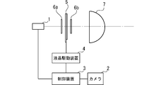
- FIG. 1 is a diagram showing a configuration of a vehicle headlight system of one embodiment.
- FIG. 2 is a plan view for explaining the configuration of the liquid crystal element.
- FIG. 3 is a plan view showing the configuration of the liquid crystal element.
- FIG. 4A is a plan view for explaining the configurations of the first pixel electrode, the first wiring portion, and the second wiring portion.
- FIG. 4B is a cross-sectional view for explaining the configurations of the first pixel electrode, the first wiring portion, and the second wiring portion.
- FIG. 5A is a plan view for explaining the configuration of the insulating film.
- FIG. 5B is a cross-sectional view for explaining the configuration of the insulating film.
- FIG. 6A is a plan view for explaining the configuration of the second pixel electrode.
- FIG. 6B is a cross-sectional view for explaining the configuration of the second pixel electrode.
- FIG. 7 is a cross-sectional view for explaining a state in which the first substrate and the second substrate are overlapped with each other.
- 8 (A) and 8 (B) are diagrams for explaining the electro-optical characteristics (VT characteristics) of the first pixel region and the second pixel region.
- FIG. 9A is a diagram showing an example of setting the voltage applied to the first pixel electrode and the second pixel electrode at room temperature.
- FIG. 9B is a graph showing the relationship between the gradation of the applied voltage shown in FIG. 9A.
- FIG. 10A is a diagram for explaining the electro-optical characteristics (VT characteristics) of the first pixel region and the second pixel region at an atmospheric temperature of 60 ° C.
- FIG. 10B is a diagram for explaining the electro-optical characteristics (VT characteristics) of the first pixel region and the second pixel region at an atmospheric temperature of 80 ° C.
- FIG. 11A is a diagram showing an example of setting the voltage applied to the first pixel electrode and the second pixel electrode in an atmosphere of 60 ° C.
- FIG. 11B is a graph showing the relationship between the gradation of the applied voltage shown in FIG. 11A.
- FIG. 12A is a diagram showing an example of setting the voltage applied to the first pixel electrode and the second pixel electrode in an atmosphere of 80 ° C.
- FIG. 12B is a graph showing the relationship between the gradation of the applied voltage shown in FIG. 12A.
- FIG. 13 (A) and 13 (B) are diagrams showing measurement examples of electro-optical characteristics with respect to obliquely incident light at room temperature.
- FIG. 14A is a diagram showing the sum of the transmittances in the viewing direction and the reverse viewing direction at the voltage at the gradation shown in FIG. 9A.
- FIG. 14B is a graph showing the relationship between the applied voltage and the gradation shown in FIG. 14A.
- FIG. 1 is a diagram showing a configuration of a vehicle headlight system of one embodiment.
- the vehicle lighting system shown in FIG. 1 includes a light source 1, a camera 2, a control device 3, a liquid crystal driving device 4, a liquid crystal element 5, a pair of polarizing plates 6a and 6b, and a projection lens 7.
- This vehicle headlight system detects the positions of front vehicles and pedestrians existing around the own vehicle based on the image taken by the camera 2, and does not illuminate a certain range including the positions of the front vehicles and the like.
- the purpose is to set a range (dimming area) and set the other range to a light irradiation range to perform selective light irradiation.
- the light source 1 is configured to include, for example, a white LED configured by combining a light emitting diode (LED) that emits blue light with a yellow phosphor.
- the light source 1 includes, for example, a plurality of white LEDs arranged in a matrix or a line.
- a laser, and a light source generally used in a vehicle lamp unit such as a light bulb or a discharge lamp can be used.
- the on / off state of the light source 1 is controlled by the control unit 3.
- the light emitted from the light source 1 enters the liquid crystal element (liquid crystal panel) 5 via the polarizing plate 6a.
- another optical system for example, a lens, a reflecting mirror, or a combination thereof
- another optical system may exist on the path from the light source 1 to the liquid crystal element 5.
- the camera 2 captures the front of the own vehicle and outputs the image (information), and is arranged at a predetermined position (for example, the upper part inside the windshield) in the own vehicle. If the vehicle is equipped with a camera for other purposes (for example, an automatic braking system), the camera may be shared.
- the control device 3 detects the position of the vehicle in front or the like by performing image processing based on the image obtained by the camera 2 that captures the front of the own vehicle, and sets the detected position of the vehicle in front or the like as the non-irradiation range.
- a light distribution pattern is set with the other region as the light irradiation range, and a control signal for forming an image corresponding to this light distribution pattern is generated and supplied to the liquid crystal drive circuit 4.
- the control device 3 is realized by executing a predetermined operation program in a computer system having, for example, a CPU, a ROM, a RAM, or the like.
- the liquid crystal driving device 4 individually controls the orientation state of the liquid crystal layer in each pixel region of the liquid crystal element 5 by supplying a driving voltage to the liquid crystal element 5 based on the control signal supplied from the control device 3. is there.
- the liquid crystal element 5 has, for example, a plurality of pixel regions (optical modulation regions) that can be individually controlled, and each pixel region corresponds to the magnitude of the voltage applied to the liquid crystal layer given by the liquid crystal driving device 4.
- the transmittance of is set variably.
- the liquid crystal element 5 includes a vertically oriented liquid crystal layer, is arranged between a pair of polarizing plates 6a and 6b arranged in orthogonal Nicols, and no voltage is applied (or a threshold value) to the liquid crystal layer.
- the voltage is as follows)
- the light transmittance is extremely low (light-shielding state)
- the light transmittance is relatively high (transmission state).
- the pair of polarizing plates 6a and 6b have their polarization axes substantially orthogonal to each other, and are arranged so as to face each other with the liquid crystal element 5 interposed therebetween.
- a normally black mode is assumed, which is an operation mode in which light is shielded (transmittance becomes extremely low) when no voltage is applied to the liquid crystal layer.
- an absorbent polarizing plate made of a general organic material iodine-based or dye-based
- the wire grid type polarizing plate is a polarizing plate formed by arranging ultrafine wires made of a metal such as aluminum. Further, the absorption type polarizing plate and the wire grid type polarizing plate may be used in combination.
- the projection lens 7 spreads an image formed by the light transmitted through the liquid crystal element 5 (an image having light and darkness corresponding to the light irradiation range and the non-irradiation range) so as to be a light distribution for headlights, and moves toward the front of the vehicle. It is for projection, and an appropriately designed lens is used. In this embodiment, an inverted projection type projector lens is used.
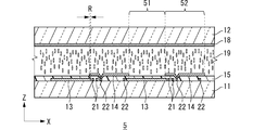
- FIG. 2 is a plan view for explaining the configuration of the liquid crystal element 5.
- FIG. 3 is a cross-sectional view showing the configuration of the liquid crystal element 5. The cross-sectional view shown in FIG. 3 corresponds to the cross-sectional view taken along the line aa shown in FIG. 2 and FIG. 4 described later.
- the liquid crystal element 5 includes a plurality of first pixel regions (first pixel portion) 51 and a plurality of second pixel regions (second pixel portion) 52.
- each second pixel area 52 is shown with a pattern so that each first pixel area 51 and each second pixel area 52 can be easily distinguished.
- the left-right direction of the liquid crystal element corresponds to the left-right direction of the light distribution projected in front of the own vehicle.
- Each first pixel area 51 and each second pixel area 52 are, for example, rectangular in a plan view as shown in FIG. Further, each of the first pixel region 51 and each second pixel region 52 is connected to the liquid crystal driving device 4, and is statically driven, for example, and the light transmittance can be individually controlled. As shown in FIG. 3, each first pixel region 51 is formed by each first pixel electrode (first individual electrode) 13 provided on the first substrate 11 side and a common electrode 18 provided on the second substrate 12 side. A voltage is applied to the liquid crystal layer 19, and the orientation direction of the liquid crystal molecules in the liquid crystal layer 19 is changed by the voltage, so that the transmittance of the light transmitted through each is changed.
- each of the second pixel regions 52 a voltage is applied to the liquid crystal layer 19 by each of the second pixel electrodes (second individual electrodes) 14 provided on the first substrate 11 side and the common electrodes 18 provided on the second substrate 12 side. Then, by changing the orientation direction of the liquid crystal molecules of the liquid crystal layer 19 by the voltage, the transmittance of the light transmitted through each is changed.
- each first pixel region 51 and each second pixel region 52 are arranged so as to be in contact with each other so that no gap is formed between them in the X direction in the plan view. ing. Further, each first pixel area 51 and each second pixel area 52 are alternately arranged one by one along the X direction in the drawing. Further, each of the first pixel region 51 and each second pixel region 52 is arranged with a gap (for example, several ⁇ m) in the Y direction in the drawing.
- the liquid crystal element 5 includes a first substrate 11, a second substrate 12, a plurality of first pixel electrodes 13 provided on the first substrate 11, and a plurality of second pixel electrodes 14.
- each of the first substrate 11 and the second substrate 12 is appropriately provided with an alignment film for regulating the alignment state of the liquid crystal layer 19.
- the first substrate 11 and the second substrate 12 are rectangular substrates in a plan view, and are arranged so as to face each other.
- a transparent substrate such as a glass substrate or a plastic substrate can be used.
- a plurality of spherical spacers made of, for example, resin are dispersedly arranged between the first substrate 11 and the second substrate 12, and the spacers keep the substrate gap at a desired size (for example, about several ⁇ m).
- a columnar spacer made of resin may be used instead of the spherical spacer.
- Each first pixel electrode 13 is provided on one surface side of the first substrate 11. Further, each first wiring portion 21 is provided on one surface side of the first substrate 11. Further, each second wiring portion 22 is provided between the first pixel electrodes 13 on one surface side of the first substrate 11.
- Each of the first pixel electrodes 13, each first wiring portion 21, and each second wiring portion 22 is configured by appropriately patterning a transparent conductive film such as indium tin oxide (ITO).
- ITO indium tin oxide
- Each second pixel electrode 14 is provided on the upper side of the insulating layer 15 on one surface side of the first substrate 11. That is, each first pixel electrode 13 is arranged closer to the first substrate 11 than each second pixel electrode 14.
- Each second pixel electrode 14 is configured by appropriately patterning a transparent conductive film such as indium tin oxide (ITO).
- ITO indium tin oxide
- the first pixel electrodes 13 and the second pixel electrodes 14 are alternately arranged one by one in the X direction in the drawing, and the ends of adjacent ones in the X direction slightly overlap each other in the Z direction in the drawing. It is provided as follows.
- the overlapping region R which is a region where the ends of the adjacent first pixel electrodes 13 and the second pixel electrodes 14 partially overlap each other, has a width of, for example, about several ⁇ m to 15 ⁇ m.
- Each first wiring portion 21 is connected to one of the first pixel electrodes 13 and is for applying a voltage to the first pixel electrode 13 (see FIG. 4 described later).
- Each of the second wiring portions 22 is connected to one of the second pixel electrodes 14 via the first insulating film 15 and is for applying a voltage to the second pixel electrode 14, and is any one of them. It is arranged at a position where it overlaps with at least a part of the second pixel electrode 14 in a plan view.
- the insulating film 15 has translucency, and is provided on one surface side of the first substrate 11 so as to cover the upper side of each first pixel electrode 13.
- the insulating film 15 is, for example, an oxide film or a nitride film such as a SiO 2 film or a SiON film, and can be formed by a vapor phase process such as a sputtering method or a solution process.
- An organic insulating film may be used as the insulating film 15.
- the film thickness of the insulating film 15 is preferably, for example, about 0.4 ⁇ m to 1.5 ⁇ m.
- the dielectric constant of the insulating film 15 is preferably higher, for example, 4 or more, and further preferably 8 or more.
- the common electrode 18 is provided on one side of the second substrate 12.
- the common electrode 18 is provided so as to overlap each of the first pixel electrode 13 and each second pixel electrode 14 in a plan view.
- the common electrode 18 is formed by appropriately patterning a transparent conductive film such as indium tin oxide (ITO).
- the liquid crystal layer 19 is interposed between the first substrate 11 and the second substrate 12.
- the liquid crystal layer 19 is constructed by using a nematic liquid crystal material having a negative dielectric anisotropy ⁇ and having fluidity.
- the liquid crystal layer 19 of the present embodiment is set so that the orientation direction of the liquid crystal molecules when no voltage is applied is substantially vertical orientation.
- alignment films are provided on one surface side of the first substrate 11 and one surface side of the second substrate 12, respectively.
- a vertical alignment film that regulates the alignment state of the liquid crystal layer 19 to vertical alignment is used.
- Each alignment film is subjected to a uniaxial alignment treatment such as a rubbing treatment, and has a uniaxial orientation regulating force that regulates the orientation of the liquid crystal molecules of the liquid crystal layer 19 in that direction.
- the directions of the alignment treatment for each alignment film are set to be staggered (anti-parallel), for example.
- FIG. 4A is a plan view for explaining the configurations of the first pixel electrode, the first wiring portion, and the second wiring portion.
- FIG. 4B is a cross-sectional view for explaining the configurations of the first pixel electrode, the first wiring portion, and the second wiring portion.
- each first pixel electrode 13 is provided on one surface side of the first substrate 11 in a region corresponding to each first pixel region 51.
- the symbols 13a, 13b, and 13c are used to distinguish the first pixel electrodes 13.
- the codes of 21a, 21b, and 21c are used to distinguish each of the first wiring portions 21, and the codes of 22a, 22b, and 22c are respectively indicated so that the second wiring portions 22 can be distinguished from each other. It is shown using.
- the first pixel electrode 13a arranged in the lower part of the figure corresponds to one first pixel region 51.
- the first wiring portion 21a is connected to the first pixel electrode 13a.
- the first wiring portion 21a extends from the lower end of the first pixel electrode 13a to the lower end of the first substrate 11.
- the first pixel electrode 13b arranged in the middle of the drawing corresponds to one first pixel region 51.
- the first wiring portion 21b is connected to the first pixel electrode 13b.
- the first wiring portion 21b extends to the lower end in the drawing of the first substrate 11 through the right side of each of the first pixel electrode 13b and the first pixel electrode 13a.
- the first pixel electrode 13c arranged in the upper part of the figure corresponds to one first pixel region 51.
- the first wiring portion 21c is connected to the first pixel electrode 13c.
- the first wiring portion 21c extends to the lower end in the drawing of the first substrate 11 through the right side of each of the first pixel electrode 13b, the first pixel electrode 13a, and the first wiring portion 21b.
- the second wiring portions 22a, 22b, 22c are arranged on the right side of the drawings of the first pixel electrodes 13a, 13b, 13c and the first wiring portions 21a, 21b, 21c.
- the second wiring portion 22a is provided between the other second wirings 22b and 22c.
- the second wiring portion 22a is associated with the second pixel electrode 14a described later, and has a shorter length in the Y direction than the other second wiring portions 22b and 22c.
- the second wiring portion 22b is provided between the first wiring portion 21c and the second wiring portion 22a.
- the second wiring portion 22b is associated with the second pixel electrode 14b described later, and has a shorter length in the Y direction than the wiring portion 22c.
- the second wiring portion 22c is provided on the right side of the second wiring portion 22a.
- the second wiring portion 22c is associated with the second pixel electrode 14c described later, and has a longer length in the Y direction than the other wiring portions 22a and 22b.
- An inter-pixel electrode 23b extending in the X direction in the figure is connected to the second wiring portion 22b.
- the inter-pixel electrode 23b is provided so as to overlap with a gap (see FIG. 2) between adjacent second pixel regions 52 in the Y direction.
- the inter-pixel electrode 23c extending in the X direction in the drawing is connected to the second wiring portion 22c.
- the inter-pixel electrode 23c is provided so as to overlap with a gap (see FIG. 2) between adjacent second pixel regions 52 in the Y direction.
- These inter-pixel electrodes 23b and 23c have the same potential as the second pixel electrodes 14b and 14c when a voltage is applied to the second pixel electrodes 14b and 14c connected to the second wiring portions 22b and 22c. become.
- the orientation direction of the liquid crystal molecules in the liquid crystal layer 19 can be changed even in the gap between the second pixel regions 52 adjacent to each other in the Y direction. , It is possible to prevent or alleviate the generation of dark lines corresponding to the gap.
- FIG. 5A is a plan view for explaining the configuration of the insulating film.
- FIG. 5B is a cross-sectional view for explaining the configuration of the insulating film.
- an insulating film 15 is provided on one surface side of the first substrate 11 so as to cover each first pixel electrode 13, each first wiring portion 21, and each second wiring portion 22. ..
- the insulating film 15 is provided with openings (through holes) 24a, 24b, 24c for exposing a part of the second wiring portions 22a, 22b, 22c. Through these openings 24a, 24b, 24c, the second wiring portions 22a, 22b, 22c and the second pixel electrodes 14a, 14b, 14c (see FIG. 6A) are physically and electrically connected to each other. Be connected.
- FIG. 6A is a plan view for explaining the configuration of the second pixel electrode.
- FIG. 6B is a cross-sectional view for explaining the configuration of the second pixel electrode.
- each second pixel electrode 14 is provided in a region corresponding to each second pixel region 52 on one surface side of the insulating film 15 of the first substrate 11.
- the reference numerals 14a, 14b, and 14c are used to distinguish the second pixel electrodes 14.
- the second pixel electrode 14a is physically and electrically connected to the second wiring portion 22a on the lower layer side via the opening 24a of the insulating film 15.
- the second pixel electrode 14b is physically and electrically connected to the second wiring portion 22b on the lower layer side via the opening 24b of the insulating film 15.
- the second pixel electrode 14c is physically and electrically connected to the second wiring portion 22c on the lower layer side via the opening 24c of the insulating film 15. Further, the second pixel electrodes 14a, 14b, and 14c are arranged so as to have a superposed region R between the first pixel electrodes 13a, 13b, and 13c as described above.
- the second pixel electrodes 14a, 14b, 14c are provided so as to overlap the first wiring portions 21b, 21c and the second wiring portions 22a, 22b, 22c in a plan view. Since the wiring portion can be arranged on the lower layer side of the pixel electrode in this way, it is not necessary to secure a space for arranging the wiring portion on the outside of each pixel region. Thereby, the gap between each pixel electrode can be eliminated.
- FIG. 7 is a cross-sectional view for explaining a state in which the first substrate and the second substrate are overlapped with each other.
- the method for manufacturing the liquid crystal element of the present embodiment will be briefly described.
- the first pixel electrodes 13 and the like are formed on one surface side of the first substrate 11.
- an insulating film 15 is formed on one surface side of the first substrate 11 so as to cover each of the first pixel electrodes 13 and the like, and the opening 24a is further formed. Etc. are formed.
- the second pixel electrodes 14 are formed on the upper side of the insulating film 15.
- the common electrode 18 is formed on one surface side of the second substrate 12.
- the one side of each of the first substrate 11 and the second substrate 12 thus obtained is appropriately oriented, and both substrates are overlapped with each other.
- the liquid crystal layer 19 is formed by injecting a liquid crystal material between the first substrate 11 and the second substrate 12. From the above, the liquid crystal element of the present embodiment is obtained (see FIG. 3).
- the first wiring portion, the second wiring portion, and the common electrode of the liquid crystal element 5 are electrically connected to the liquid crystal driving device 4, and the liquid crystal driving device 4 connects to the liquid crystal element 5 based on the control signal supplied from the control device 3. It is configured to be able to supply the drive voltage.
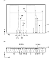
- FIG. 8 (A) and 8 (B) are diagrams for explaining the electro-optical characteristics (VT characteristics) of the first pixel region and the second pixel region.
- the measurement point passing through the first pixel region 51 is designated as B
- the measuring point passing through the second pixel region 52 is defined as A
- An example of measuring the optical characteristics is shown in FIG. 8 (B). Comparing the first pixel region 51 and the second pixel region 52, in the first pixel region 51, the voltage from the first pixel electrode 13 is divided by the insulating film 15 and applied to the liquid crystal layer 19. In the second pixel region 52, the voltage from the second pixel electrode 14 is directly applied to the liquid crystal layer 19.
- the voltage applied to the first pixel region 51 may be set to a value relatively larger than the voltage corresponding to the voltage division in the insulating film 15.
- V down (C in / (C in + C LC )) ⁇ V up
- C in and C LC can be expressed as follows.
- FIG. 9A is a diagram showing an example of setting the voltage applied to the first pixel electrode and the second pixel electrode at room temperature. Further, FIG. 9B is a graph showing the relationship between the gradations of the applied voltage shown in FIG. 9A.
- the liquid crystal element according to the above embodiment the liquid crystal element of the example in which the layer thickness of the liquid crystal layer 19 is 4 ⁇ m and the refractive index anisotropy ⁇ n is about 0.13 is used (the same applies hereinafter). ..
- FIG. 9A shows an applied voltage at which a desired transmittance can be obtained when the gradation is divided into 9 stages. It can be seen that the required voltages are different between the measurement point A and the measurement point B.
- the difference in transmittance at each of the measurement points A and B is within ⁇ 1.5% in the range of gradation "0" to gradation "8", and the transmittance is substantially the same. It can be said that there is. Further, the difference in transmittance is within ⁇ 1.0% except for the gradation "3", and it can be said that the transmittances are substantially the same. In the case of forming high-intensity irradiation light in front of the vehicle as in the present embodiment, if the difference in transmittance is within ⁇ 2.0%, it can be said that the transmittances are substantially the same.
- FIG. 10A is a diagram for explaining the electro-optical characteristics (VT characteristics) of the first pixel region and the second pixel region at an atmospheric temperature of 60 ° C.
- FIG. 10B is a diagram for explaining the electro-optical characteristics (VT characteristics) of the first pixel region and the second pixel region at an atmospheric temperature of 80 ° C. It can be seen that, as in the case of room temperature described above, there is a difference in electro-optical characteristics between the first pixel region 51 (measurement point B) and the second pixel region 52 (measurement point A) even in a high temperature atmosphere.
- FIG. 11A is a diagram showing an example of setting the voltage applied to the first pixel electrode and the second pixel electrode in an atmosphere of 60 ° C. Further, FIG. 11B is a graph showing the relationship between the gradation of the applied voltage shown in FIG. 11A.
- FIG. 12A is a diagram showing an example of setting the voltage applied to the first pixel electrode and the second pixel electrode in an atmosphere of 80 ° C. Further, FIG. 12B is a graph showing the relationship between the gradation of the applied voltage shown in FIG. 12A.
- electro-optics in each of the first pixel region 51 and the second pixel region 52 it is possible to reduce the difference in characteristics and suppress unevenness in the brightness of the irradiation light.
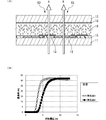
- FIG. 13 (A) and 13 (B) are diagrams showing measurement examples of electro-optical characteristics with respect to obliquely incident light at room temperature.
- FIG. 13 (A) shows the electro-optic characteristics when light is incident from the 20 ° direction with respect to the substrate normal in the viewing direction
- FIG. 13 (B) shows the electro-optical characteristics in the reverse viewing direction with reference to the substrate normal. This is an electro-optical characteristic when light is incident from the 20 ° direction.
- FIG. 14A is a diagram showing the sum of the transmittances in the viewing direction and the reverse viewing direction at the voltage at the gradation shown in FIG. 9A described above.
- FIG. 14B is a graph showing the relationship between the applied voltage and the gradation shown in FIG. 14A.
- the dark line caused by the gap between the pixel regions in the irradiation light to the front of the vehicle It is possible to prevent the occurrence and improve the appearance of the light distribution pattern.
- the present invention is not limited to the contents of the above-described embodiment, and can be variously modified and implemented within the scope of the gist of the present invention.
- the boundaries between the pixel regions of the liquid crystal element are arranged vertically and horizontally has been illustrated, but the boundaries between the pixel regions may be arranged in an oblique direction. Further, the boundary is not limited to a straight line, but may be a curved line.
- vertical orientation is exemplified as the orientation mode of the liquid crystal layer of the liquid crystal element, but the orientation mode is not limited, and for example, a twist orientation mode may be used.
- an optical compensation plate such as a so-called C plate may be provided on one side or both sides of the liquid crystal element.
- the liquid crystal element having each pixel region arranged along the two directions (XY directions) of up, down, left and right is illustrated, but the liquid crystal elements are arranged along at least one direction (for example, the X direction).
- the liquid crystal element may be configured to have each pixel region.
Abstract
液晶素子等を用いて配光パターンを制御する照明装置における配光パターンの見栄えを向上させること。 第1基板と、前記第1基板に対向配置された第2基板と、前記第1基板の第2基板側の面に配置された第1画素領域に対応する第1画素電極と、前記第1基板の第2基板側の面に配置された第2画素領域に対応する第2画素電極と、前記第2基板の前記第1基板側に配置された共通電極と、前記第1画素電極及び前記第2画素電極と前記共通電極との間に配置された液晶層と、を備え、前記第1画素電極と前記第2画素電極は、前記第1基板上において異なる層に設けられており、各々の端部同士が平面視において部分的に重なるように配置されている液晶素子である。
Description
本発明は、例えば車両前方などに所望のパターンで光照射を行うための装置(システム)並びに当該装置(システム)に用いて好適な液晶素子に関する。
特開2005-183327号公報(特許文献1)には、少なくとも一つのLEDから成る発光部と、上記発光部から前方に向かって照射される光の一部を遮断して、車両前照灯用の配光パターンに適したカットオフを形成する遮光部と、を含んでおり、上記遮光部が、調光機能を備えた電気光学素子と、この電気光学素子を調光制御する制御部と、から構成されていて、この制御部による電気光学素子の電気的スイッチング制御によって、調光部分を選択的に調光することにより、配光パターンの形状を変化させるように構成された車両前照灯が開示されている。電気光学素子としては、例えば液晶素子が用いられている。
上記のような車両用灯具において、液晶素子等の電気光学素子は、選択的な調光を実現するために複数の画素電極を有して構成される。これらの画素電極は、各々個別に電圧を印加し得るように互いに分離しており、各々の間には電気的絶縁を図るための隙間が設けられている。このとき、画素電極同士の隙間は、その形成精度にもよるが例えば10μm程度となる。また、画素電極の列を3つ以上設けるような場合には、中間列の各画素電極に電圧を与えるための配線部を画素電極間に通す必要が生じるため、画素電極同士の隙間はより大きくなる。画素電極同士の隙間は、画像形成に寄与しない部分であり、配光パターン内に暗線を発生させる要因となる。車両用灯具では、電気光学素子によって形成された画像(配光パターンに対応した画像)をレンズ等によって拡大して車両前方へ投影するので、上記のような暗線も拡大されて視認しやすくなるため、配光パターンの見栄えが悪くなるという不都合がある。これに対して、画素電極同士の隙間をより狭めるという解決策も考え得るが、その場合、製造コストの上昇を招き、また画素電極同士の短絡等の不具合を生じやすくなり得るために好ましくない。また、画素電極間に通す配線部の幅をより細くするという解決策も考え得るが、その場合、配線部の抵抗値が上昇してしまい画素電極に必要十分な電圧を印加しにくくなり、また細線化による断線の発生確率も上昇するために好ましくない。なお、このような不都合は車両用灯具に限らず、液晶素子等を用いて配光パターンを制御する照明装置一般においても同様である。
本発明に係る具体的態様は、液晶素子等を用いて配光パターンを制御する照明装置における配光パターンの見栄えを向上させることが可能な技術を提供することを目的の1つとする。
[1]本発明に係る一態様の液晶素子は、(a)第1基板と、(b)前記第1基板に対向配置された第2基板と、(c)前記第1基板の第2基板側の面に配置された第1画素領域に対応する第1画素電極と、(d)前記第1基板の第2基板側の面に配置された第2画素領域に対応する第2画素電極と、(e)前記第2基板の前記第1基板側に配置された共通電極と、(f)前記第1画素電極及び前記第2画素電極と前記共通電極との間に配置された液晶層と、を備え、(g)前記第1画素電極と前記第2画素電極は、前記第1基板上において異なる層に設けられており、各々の端部同士が平面視において部分的に重なるように配置されている、液晶素子である。
[2]本発明に係る一態様の照明装置は、(a)配光パターンを可変に設定可能な照明装置であって、(b)光源と、(c)前記光源からの光を用いて前記配光パターンに対応する画像を形成する液晶素子と、(d)前記液晶素子によって形成された前記画像を投影する光学系と、を含み、(e)前記液晶素子として前記何れかに記載の液晶素子を用いる、照明装置である。
[2]本発明に係る一態様の照明装置は、(a)配光パターンを可変に設定可能な照明装置であって、(b)光源と、(c)前記光源からの光を用いて前記配光パターンに対応する画像を形成する液晶素子と、(d)前記液晶素子によって形成された前記画像を投影する光学系と、を含み、(e)前記液晶素子として前記何れかに記載の液晶素子を用いる、照明装置である。
上記構成によれば、液晶素子等を用いて配光パターンを制御する照明装置における配光パターンの見栄えを向上させることが可能となる。
図1は、一実施形態の車両用前照灯システムの構成を示す図である。図1に示す車両用灯具システムは、光源1、カメラ2、制御装置3、液晶駆動装置4、液晶素子5、一対の偏光板6a、6b、投影レンズ7を含んで構成されている。この車両用前照灯システムは、カメラ2によって撮影される画像に基づいて自車両の周囲に存在する前方車両や歩行者等の位置を検出し、前方車両等の位置を含む一定範囲を非照射範囲(減光領域)に設定し、それ以外の範囲を光照射範囲に設定して選択的な光照射を行うためのものである。
光源1は、例えば青色光を放出する発光ダイオード(LED)に黄色蛍光体を組み合わせて構成された白色LEDを含んで構成されている。光源1は、例えば、マトリクス状あるいはライン状に配列された複数の白色LEDを備える。なお、光源1としてはLEDのほかに、レーザー、さらには電球や放電灯など車両用ランプユニットに一般的に使用されている光源が使用可能である。光源1の点消灯状態は制御部3によって制御される。光源1から出射する光は、偏光板6aを介して液晶素子(液晶パネル)5に入射する。なお、光源1から液晶素子5へ至る経路上に他の光学系(例えば、レンズや反射鏡、さらにはそれらを組み合わせたもの)が存在してもよい。
カメラ2は、自車両の前方を撮影してその画像(情報)を出力するものであり、自車両内の所定位置(例えば、フロントガラス内側上部)に配置されている。なお、他の用途(例えば、自動ブレーキシステム等)のためのカメラが自車両に備わっている場合にはそのカメラを共用してもよい。
制御装置3は、自車両の前方を撮影するカメラ2によって得られる画像に基づいて画像処理を行うことによって前方車両等の位置を検出し、検出された前方車両等の位置を非照射範囲とし、それ以外の領域を光照射範囲とした配光パターンを設定し、この配光パターンに対応した像を形成するための制御信号を生成して液晶駆動回路4へ供給する。この制御装置3は、例えばCPU、ROM、RAM等を有するコンピュータシステムにおいて所定の動作プログラムを実行させることによって実現される。
液晶駆動装置4は、制御装置3から供給される制御信号に基づいて液晶素子5に駆動電圧を供給することにより、液晶素子5の各画素領域における液晶層の配向状態を個別に制御するものである。
液晶素子5は、例えば、それぞれ個別に制御可能な複数の画素領域(光変調領域)を有しており、液晶駆動装置4によって与えられる液晶層への印加電圧の大きさに応じて各画素領域の透過率が可変に設定される。この液晶素子5に光源1からの光が照射されることにより、上記した光照射範囲と非照射範囲に対応した明暗を有する像が形成される。例えば、液晶素子5は、垂直配向型の液晶層を備えるものであり、直交ニコル配置された一対の偏光板6a、6bの間に配置されており、液晶層への電圧が無印加(あるいは閾値以下の電圧)である場合に光透過率が極めて低い状態(遮光状態)となり、液晶層へ電圧が印加された場合に光透過率が相対的に高い状態(透過状態)となるものである。
一対の偏光板6a、6bは、例えば互いの偏光軸を略直交させており、液晶素子5を挟んで対向配置されている。本実施形態では、液晶層に電圧無印加としているときに光が遮光される(透過率が極めて低くなる)動作モードであるノーマリーブラックモードを想定する。各偏光板6a、6bとしては、例えば一般的な有機材料(ヨウ素系、染料系)からなる吸収型偏光板を用いることができる。また、耐熱性を重視したい場合には、ワイヤーグリッド型偏光板を用いることも好ましい。ワイヤーグリッド型偏光板とはアルミニウム等の金属による極細線を配列してなる偏光板である。また、吸収型偏光板とワイヤーグリッド型偏光板を重ねて用いてもよい。
投影レンズ7は、液晶素子5を透過する光によって形成される像(光照射範囲と非照射範囲に対応した明暗を有する像)をヘッドライト用配光になるように広げて自車両の前方へ投影するものであり、適宜設計されたレンズが用いられる。本実施形態では、反転投影型のプロジェクターレンズが用いられる。
図2は、液晶素子5の構成を説明するための平面図である。図3は、液晶素子5の構成を示す断面図である。なお、図3に示す断面図は、図2および後述する図4に示すa-a線における断面に対応している。各図に示すように、液晶素子5は、複数の第1画素領域(第1画素部)51と、複数の第2画素領域(第2画素部)52を含んで構成されている。なお、図2では、各第1画素領域51と各第2画素領域52を識別しやすいように各第2画素領域52に模様を付して示している。なお、液晶素子の左右方向が自車両前方に投影される配光の左右方向に対応している。
各第1画素領域51、各第2画素領域52は、図2に示すように平面視において例えば矩形状である。また、各第1画素領域51、各第2画素領域52は、液晶駆動装置4と接続されており、例えばスタティック駆動されてそれぞれ個別に光の透過率を制御可能である。図3に示すように、各第1画素領域51は、第1基板11側に設けられた各第1画素電極(第1個別電極)13と第2基板12側に設けられた共通電極18によって液晶層19に電圧を印加し、当該電圧によって液晶層19の液晶分子の配向方向を変化させることにより、各々を透過する光の透過率を変化させる。各第2画素領域52は、第1基板11側に設けられた各第2画素電極(第2個別電極)14と第2基板12側に設けられた共通電極18によって液晶層19に電圧を印加し、当該電圧によって液晶層19の液晶分子の配向方向を変化させることにより、各々を透過する光の透過率を変化させる。
図2に示すように、各第1画素領域51、各第2画素領域52は、平面視において図中のX方向において互いの間に隙間が生じないように互いの一端部を接して配置されている。また、各第1画素領域51と各第2画素領域52は、図中X方向に沿って1つずつ交互に配置されている。また、各第1画素領域51、各第2画素領域52は、各々、図中Y方向においては隙間(例えば数μm)を設けて配置されている。
図3に示すように、液晶素子5は、対向配置された第1基板11および第2基板12、第1基板11に設けられた複数の第1画素電極13、複数の第2画素電極14、絶縁膜15、複数の第1配線部21および複数の第2配線部22と、第2基板12に設けられた共通電極18と、第1基板11と第2基板12の間に配置された液晶層19と、を含んで構成されている。なお、説明の便宜上、図示を省略しているが、第1基板11、第2基板12には、それぞれ液晶層19の配向状態を規制するための配向膜が適宜設けられる。
第1基板11および第2基板12は、それぞれ、平面視において矩形状の基板であり、互いに対向して配置されている。各基板としては、例えばガラス基板、プラスチック基板等の透明基板を用いることができる。第1基板11と第2基板12の間には、例えば樹脂などからなる複数の球状スペーサーが分散配置されており、それらスペーサーによって基板間隙が所望の大きさ(例えば数μm程度)に保たれている。なお、球状スペーサーに代えて樹脂からなる柱状スペーサーが用いられてもよい。
各第1画素電極13は、第1基板11の一面側に設けられている。また、各第1配線部21は、第1基板11の一面側に設けられている。また、各第2配線部22は、第1基板11の一面側において各第1画素電極13の間に設けられている。各第1画素電極13、各第1配線部21および各第2配線部22は、例えばインジウム錫酸化物(ITO)などの透明導電膜を適宜パターニングすることによって構成されている。各第1画素電極13と共通電極18との重なる領域のそれぞれにおいて上記した第1画素領域51が画定されている。
各第2画素電極14は、第1基板11の一面側において絶縁層15の上側に設けられている。すなわち、各第1画素電極13は、各第2画素電極14よりも第1基板11側に配置されている。各第2画素電極14は、例えばインジウム錫酸化物(ITO)などの透明導電膜を適宜パターニングすることによって構成されている。各第2画素電極14と共通電極18との重なる領域のそれぞれにおいて上記した第2画素領域52が画定されている。
各第1画素電極13と各第2画素電極14は、図中X方向において1つずつ交互に配置されており、かつX方向に隣り合うもの同士の端部が図中Z方向において僅かに重なるように設けられている。隣り合う第1画素電極13と第2画素電極14の端部同士が部分的に重なった領域である重畳領域Rは、例えば数μm~15μm程度の幅である。このような重畳領域Rを設けることで製造時における位置ズレの許容度が高まり、第1画素領域51と第2画素領域52との隙間(図2のX方向における隙間)を確実になくすことができる。
各第1配線部21は、いずれかの第1画素電極13と接続されて当該第1画素電極13に対して電圧を印加するためのものである(後述する図4参照)。各第2配線部22は、第1絶縁膜15を介していずれかの第2画素電極14と接続されて当該第2画素電極14に対して電圧を印加するためのものであり、何れかの第2画素電極14の少なくとも一部と平面視において重なる位置に配置されている。
絶縁膜15は、透光性を有しており、第1基板11の一面側において各第1画素電極13の上側にこれらを覆うようにして設けられている。この絶縁膜15は、例えばSiO2膜、SiON膜等の酸化膜や窒化膜であり、スパッタ法などの気相プロセスあるいは溶液プロセスにより形成することができる。なお、この絶縁膜15としては有機絶縁膜を用いてもよい。絶縁膜15の膜厚は例えば0.4μm~1.5μm程度が望ましい。また絶縁膜15の誘電率はより高いほうが望ましく、例えば4以上、さらには8以上であることが望ましい。
共通電極18は、第2基板12の一面側に設けられている。この共通電極18は、各第1画素電極13および各第2画素電極14のすべてと平面視において重なるように設けられている。共通電極18は、例えばインジウム錫酸化物(ITO)などの透明導電膜を適宜パターニングすることによって構成されている。
液晶層19は、第1基板11と第2基板12の間に介在している。本実施形態においては、誘電率異方性Δεが負であり、流動性を有するネマティック液晶材料を用いて液晶層19が構成される。本実施形態の液晶層19は、電圧無印加時における液晶分子の配向方向が略垂直配向となるように設定されている。
なお、上記のように第1基板11の一面側と第2基板12の一面側にはそれぞれ配向膜が設けられている。各配向膜としては、液晶層19の配向状態を垂直配向に規制する垂直配向膜が用いられる。各配向膜にはラビング処理等の一軸配向処理が施されており、その方向へ液晶層19の液晶分子の配向を規定する一軸配向規制力を有している。各配向膜への配向処理の方向は、例えば互い違い(アンチパラレル)となるように設定される。
図4(A)は、第1画素電極、第1配線部および第2配線部の構成を説明するための平面図である。また、図4(B)は、第1画素電極、第1配線部および第2配線部の構成を説明するための断面図である。図4(A)に示すように、第1基板11の一面側には、各第1画素領域51に対応する領域に各第1画素電極13が設けられている。図中では、各第1画素電極13を区別できるようにそれぞれに13a、13b、13cの符号を用いて示している。また、各第1配線部21を区別できるようにそれぞれに21a、21b、21cの符号を用いて示しており、各第2配線部22を区別できるようにそれぞれに22a、22b、22cの符号を用いて示している。
図中の下段に配置される第1画素電極13aは、1つの第1画素領域51に対応するものである。この第1画素電極13aには第1配線部21aが接続されている。第1配線部21aは、第1画素電極13aの下端から第1基板11の下端まで延在している。図中の中段に配置される第1画素電極13bは、1つの第1画素領域51に対応するものである。この第1画素電極13bには第1配線部21bが接続されている。第1配線部21bは、第1画素電極13bおよび第1画素電極13aの各々の右側を通って第1基板11の図中下端まで延在している。図中の上段に配置される第1画素電極13cは、1つの第1画素領域51に対応するものである。この第1画素電極13cには第1配線部21cが接続されている。第1配線部21cは、第1画素電極13b、第1画素電極13aおよび第1配線部21bの各々の右側を通って第1基板11の図中下端まで延在している。
各第2配線部22a、22b、22cは、各第1画素電極13a、13b、13cおよび各第1配線部21a、21b、21cの図中右側に配置されている。詳細には、第2配線部22aは、他の第2配線22b、22cの間に設けられている。この第2配線部22aは、後述する第2画素電極14aに対応付けられたものであり、他の第2配線部22b、22cよりもY方向長さが短い。第2配線部22bは、第1配線部21cと第2配線部22aの間に設けられている。この第2配線部22bは、後述する第2画素電極14bに対応付けられたものであり、配線部22cよりもY方向長さが短い。第2配線部22cは、第2配線部22aの右側に設けられている。この第2配線部22cは、後述する第2画素電極14cに対応付けられたものであり、他の配線部22a、22bよりもY方向長さが長い。
第2配線部22bには、図中X方向に延在する画素間電極23bが接続されている。この画素間電極23bは、Y方向において隣り合う第2画素領域52の相互間の隙間(図2参照)と重なるように設けられている。同様に、第2配線部22cには、図中X方向に延在する画素間電極23cが接続されている。この画素間電極23cは、Y方向において隣り合う第2画素領域52の相互間の隙間(図2参照)と重なるように設けられている。これらの画素間電極23b、23cは、各第2配線部22b、22cと接続される各第2画素電極14b、14cに電圧が印加される際に、これら第2画素電極14b、14cと同電位になる。このため、各第2画素電極14b、14cへの電圧印加時に、Y方向において隣り合う第2画素領域52の相互間の隙間においても液晶層19の液晶分子の配向方向を変化させることが可能となり、当該隙間に対応した暗線の発生を防ぎ、あるいは緩和することができる。
図5(A)は、絶縁膜の構成を説明するための平面図である。図5(B)は、絶縁膜の構成を説明するための断面図である。各図に示すように、第1基板11の一面側には、各第1画素電極13、各第1配線部21、各第2配線部22を覆うようにして絶縁膜15が設けられている。そして、この絶縁膜15には、各第2配線部22a、22b、22cの一部を露出させるための開口部(スルーホール)24a、24b、24cが設けられている。これらの開口部24a、24b、24cを介して、各第2配線部22a、22b、22cと各第2画素電極14a、14b、14c(図6(A)参照)とが物理的および電気的に接続される。
図6(A)は、第2画素電極の構成を説明するための平面図である。図6(B)は、第2画素電極の構成を説明するための断面図である。各図に示すように、第1基板11の絶縁膜15の一面側には、各第2画素領域52に対応する領域に各第2画素電極14が設けられている。図中では、各第2画素電極14を区別できるように、それぞれに14a、14b、14cの符号を用いて示している。第2画素電極14aは、絶縁膜15の開口部24aを介して下層側の第2配線部22aと物理的および電気的に接続されている。第2画素電極14bは、絶縁膜15の開口部24bを介して下層側の第2配線部22bと物理的および電気的に接続されている。第2画素電極14cは、絶縁膜15の開口部24cを介して下層側の第2配線部22cと物理的および電気的に接続されている。また、各第2画素電極14a、14b、14cは、上記のように各第1画素電極13a、13b、13cとの間で重畳領域Rを有するように配置されている。
また、第2画素電極14a、14b、14cは、第1配線部21b、21c、第2配線部22a、22b、22cと平面視において重なるように設けられている。このように配線部を画素電極の下層側に配置できるので、各画素領域の外側に配線部を配置するためのスペースを確保する必要がなくなる。それにより、各画素電極間の隙間をなくすことができる。
図7は、第1基板と第2基板を重ね合わせた状態を説明するための断面図である。ここで、本実施形態の液晶素子の製造方法について簡単に説明する。まず、上記図4(A)、図4(B)に示したように、第1基板11の一面側に各第1画素電極13等を形成する。次いで、上記図5(A)、図5(B)に示したように、第1基板11の一面側に各第1画素電極13等を覆うように絶縁膜15を形成し、さらに開口部24a等を形成する。さらに、上記図6(A)、図6(B)に示したように、絶縁膜15の上側に各第2画素電極14を形成する。他方で、第2基板12の一面側に共通電極18を形成する。このようにして得られた第1基板11と第2基板12の各々の一面側に適宜配向処理を施し、両基板を重ね合わせる。これらの第1基板11と第2基板12の間に液晶材料を注入することによって液晶層19を形成する。以上により、本実施形態の液晶素子が得られる(図3参照)。液晶素子5の第1配線部、第2配線部および共通電極は、液晶駆動装置4に電気的に接続され、制御装置3から供給される制御信号に基づいて液晶駆動装置4から液晶素子5に駆動電圧を供給できるように構成される。
図8(A)、図8(B)は、第1画素領域と第2画素領域の電気光学特性(VT特性)について説明するための図である。図8(A)に示すように、第1画素領域51を通る測定点をB、第2画素領域52を通る測定点をAとし、室温(25℃)にて各測定点A、Bにおける電気光学特性を計測した例を図8(B)に示している。第1画素領域51と第2画素領域52を比較すると、第1画素領域51では第1画素電極13からの電圧が絶縁膜15において分圧されて液晶層19へ印加されるのに対して、第2画素領域52では第2画素電極14からの電圧が直接的に液晶層19へ印加される。この分圧される電圧の有無に起因して、第1画素領域51と第2画素領域52では電気光学特性に差異が生じる。このため、階調表示領域(例えば、印加電圧3~8Vくらいの間)において第1画素領域51と第2画素領域52で同じ透過率を得るためには、第2画素領域52(測定点A)に印加する電圧よりも第1画素領域51(測定点B)に印加する電圧を、絶縁膜15における分圧に相当する電圧に対応して相対的に大きい値に設定すればよい。
具体的には、絶縁層15の静電容量をCin、液晶層19の静電容量をCLCとし、第1画素電極13に印加する電圧をVdown、第2画素電極14に印加する電圧をVupとすると、これらの関係は以下のように表せる。
Vdown=(Cin/(Cin+CLC))・Vup
Vdown=(Cin/(Cin+CLC))・Vup
ここで、電極面積をS、絶縁層15の誘電率をεin、絶縁層15の膜厚をdin、液晶層19の誘電率をεLC、液晶層19の膜厚をdLCとすると、CinおよびCLCはそれぞれ以下のように表せる。
Cin=(S/din)・εin
CLC=(S/dLC)・εLC
Cin=(S/din)・εin
CLC=(S/dLC)・εLC
したがって、理論的には上記関係式を満たすように第1画素電極13と第2画素電極14への印加電圧を設定すれば、第1画素領域51と第2画素領域52の各々における電気光学特性の差異を解消し、照射光の明るさのムラを抑制することができる。
図9(A)は、室温下における第1画素電極と第2画素電極への印加電圧の設定例を示す図である。また、図9(B)は、図9(A)に示す印加電圧を階調の関係をグラフで示した図である。なお、ここでは、上記実施形態に係る液晶素子において、液晶層19の層厚を4μm、屈折率異方性Δnを約0.13とした実施例の液晶素子を用いた(以下においても同様)。図9(A)では、階調を9段階に分けた場合において、所望の透過率を得られる印加電圧が示されている。測定点Aと測定点Bでは必要な電圧が異なることが分かる。例えば、階調「5」の透過率を得る場合、測定点Aに対応する第2画素電極14には3.8Vを印加し、測定点Bに対応する第1画素電極13には5.4Vを印加すればよい。他の階調においても同様である。このように、第1画素電極13と第2画素電極14への印加電圧に差をつけて設定することで、第1画素領域51と第2画素領域52の各々における電気光学特性の差を低減し、照射光の明るさのムラを抑制することができる。図示の例では、階調「0」から階調「8」の範囲で測定点A、Bの各々における透過率の差が±1.5%以内に収まっており、実質的に同一透過率であるといえる。さらに、階調「3」を除いては透過率の差が±1.0%以内であり、実質的に同一透過率であるといえる。本実施形態のように車両の前方へ高輝度の照射光を形成する場合であれば、透過率の差が±2.0%以内であれば、実質的に同一透過率であるといえる。
図10(A)は、雰囲気温度60℃における第1画素領域と第2画素領域の電気光学特性(VT特性)について説明するための図である。また、図10(B)は、雰囲気温度80℃における第1画素領域と第2画素領域の電気光学特性(VT特性)について説明するための図である。上記した室温の場合と同様に、高温雰囲気下においても第1画素領域51(測定点B)と第2画素領域52(測定点A)で電気光学特性に差を生じることが分かる。
図11(A)は、60℃雰囲気下における第1画素電極と第2画素電極への印加電圧の設定例を示す図である。また、図11(B)は、図11(A)に示す印加電圧を階調の関係をグラフで示した図である。図12(A)は、80℃雰囲気下における第1画素電極と第2画素電極への印加電圧の設定例を示す図である。また、図12(B)は、図12(A)に示す印加電圧を階調の関係をグラフで示した図である。上記した室温の場合と同様に、第1画素電極13と第2画素電極14への印加電圧に差をつけて設定することで、第1画素領域51と第2画素領域52の各々における電気光学特性の差を低減し、照射光の明るさのムラを抑制することができる。
図13(A)、図13(B)は、室温下における斜め入射光に対する電気光学特性の測定例を示す図である。図13(A)は、視認方向について基板法線を基準に20°方向から光を入射させた場合の電気光学特性であり、図13(B)は、逆視認方向について基板法線を基準に20°方向から光を入射させた場合の電気光学特性である。また、図14(A)は、上記した図9(A)に示した階調での電圧における視認方向と逆視認方向の透過率の和を示した図である。図14(B)は、図14(A)に示す印加電圧と階調の関係をグラフで示した図である。これらの結果より、室温下において正面方向から視認する場合と同じ階調電圧を印加することで、視角方向が変わっても測定点A、Bともに同等の明るさで光を照射できることが分かる。階調の直線性はやや失われているものの、階調反転しないことも分かる。ここでは、視角の最も厳しい方向においても法線方向の場合に対して最適化した電圧と同じ階調電圧を用いることができるということが分かる。
以上のような実施形態によれば、平面視において、少なくとも液晶素子の左右方向における画素領域間の隙間をなくすことができることから、車両前方への照射光において画素領域間の隙間に起因する暗線の発生を防ぎ、配光パターンの見栄えを向上させることが可能となる。
なお、本発明は上記した実施形態の内容に限定されるものではなく、本発明の要旨の範囲内において種々に変形して実施をすることが可能である。例えば、上記した実施形態では液晶素子の各画素領域同士の境界が上下左右に配置されている場合について例示していたが、各画素領域同士の境界は斜め方向に配置されていてもよい。また、境界は直線状に限られず、曲線状であってもよい。また、上記した実施形態では液晶素子の液晶層の配向モードとして垂直配向を例示していたが配向モードに限定はなく、例えば捻れ配向モードであってもよい。さらに、液晶素子の片側ないし両側にいわゆるCプレートなどの光学補償板が設けられていてもよい。また、上記した実施形態では上下左右の2方向(XY方向)に沿って配列された各画素領域を有する液晶素子を例示していたが、少なくとも1方向(例えばX方向)に沿って配列された各画素領域を有するように液晶素子を構成してもよい。
1:光源、2:カメラ、3:制御装置、4:液晶駆動装置、5:液晶素子、6a、6b:偏光板、7:投影レンズ、11:第1基板、12:第2基板、13、13a、13b、13c:第1画素電極、14、14a、14b、14c:第2画素電極、15:絶縁膜、18:共通電極、19:液晶層、21、21a、21b、21c:第1配線部、22、22a、22b、22c:第2配線部、23b、23c:画素間電極、24、24a、24b、24c:開口部(スルーホール)、51:第1画素領域、52:第2画素領域
Claims (6)
- 第1基板と、
前記第1基板に対向配置された第2基板と、
前記第1基板の第2基板側の面に配置された第1画素領域に対応する第1画素電極と、
前記第1基板の第2基板側の面に配置された第2画素領域に対応する第2画素電極と、
前記第2基板の前記第1基板側に配置された共通電極と、
前記第1画素電極及び前記第2画素電極と前記共通電極との間に配置された液晶層と、を備え、
前記第1画素電極と前記第2画素電極は、前記第1基板上において異なる層に設けられており、各々の端部同士が平面視において部分的に重なるように配置されている、
液晶素子。 - 前記第1画素電極は、前記第1基板上において前記第2画素電極よりも前記第1基板側に配置されている、
請求項1に記載の液晶素子。 - 更に、前記第1画素電極、前記第2画素電極および前記共通電極に電気的に接続され、前記第1画素電極と前記共通電極との間、および、前記第2画素電極と前記共通電極との間に電圧を印加するための液晶駆動装置と、を備え、
前記第1画素領域と前記第2画素領域とを同一階調にする際に、前記液晶駆動装置によって前記第1画素電極と前記共通電極との間に印加する第1電圧を前記第2画素電極と前記共通電極に印加する第2電圧よりも高く設定する、
請求項2に記載の液晶素子。 - 前記第1基板上において前記第1画素電極と前記第2画素電極との間に設けられた絶縁膜を更に含み、
前記第1電圧と前記第2電圧の差は、前記絶縁膜を介して前記第1画素電極から前記液晶層に電圧を印加する際に当該絶縁膜によって分圧される電圧に相当するものである、
請求項3に記載の液晶素子。 - 前記第1画素電極に接続される第1配線部と、
前記第2画素電極に接続される第2配線部と、
を更に含み、
前記第1配線部及び前記第2配線部は、前記第1基板上において前記絶縁膜を介して前記第2画素電極よりも前記第1基板側に配置されており、
前記第2配線部は、前記絶縁膜に設けられた開口部を介して前記第2画素電極と接続されている、
請求項4に記載の液晶素子。 - 配光パターンを可変に設定可能な照明装置であって、
光源と、
前記光源からの光を用いて前記配光パターンに対応する画像を形成する液晶素子と、
前記液晶素子によって形成された前記画像を投影する光学系と、
を含み、
前記液晶素子として請求項1~5の何れかに記載の液晶素子を用いる、
照明装置。
Priority Applications (3)
| Application Number | Priority Date | Filing Date | Title |
|---|---|---|---|
| EP20833071.2A EP3992704A4 (en) | 2019-06-28 | 2020-06-15 | LIQUID CRYSTAL ELEMENT AND LIGHTING DEVICE |
| US17/623,121 US11906854B2 (en) | 2019-06-28 | 2020-06-15 | Liquid crystal element, lighting apparatus |
| CN202080042906.3A CN114008522B (zh) | 2019-06-28 | 2020-06-15 | 液晶元件、照明装置 |
Applications Claiming Priority (2)
| Application Number | Priority Date | Filing Date | Title |
|---|---|---|---|
| JP2019-121990 | 2019-06-28 | ||
| JP2019121990A JP7345293B2 (ja) | 2019-06-28 | 2019-06-28 | 液晶素子、照明装置 |
Publications (1)
| Publication Number | Publication Date |
|---|---|
| WO2020262066A1 true WO2020262066A1 (ja) | 2020-12-30 |
Family
ID=74061945
Family Applications (1)
| Application Number | Title | Priority Date | Filing Date |
|---|---|---|---|
| PCT/JP2020/023374 WO2020262066A1 (ja) | 2019-06-28 | 2020-06-15 | 液晶素子、照明装置 |
Country Status (5)
| Country | Link |
|---|---|
| US (1) | US11906854B2 (ja) |
| EP (1) | EP3992704A4 (ja) |
| JP (1) | JP7345293B2 (ja) |
| CN (1) | CN114008522B (ja) |
| WO (1) | WO2020262066A1 (ja) |
Families Citing this family (1)
| Publication number | Priority date | Publication date | Assignee | Title |
|---|---|---|---|---|
| JP2023085841A (ja) * | 2021-12-09 | 2023-06-21 | スタンレー電気株式会社 | 液晶装置、液晶装置の駆動方法 |
Citations (5)
| Publication number | Priority date | Publication date | Assignee | Title |
|---|---|---|---|---|
| JPH06160875A (ja) * | 1992-11-20 | 1994-06-07 | Seiko Epson Corp | 液晶表示装置 |
| JPH1144893A (ja) * | 1997-04-18 | 1999-02-16 | Hyundai Electron Ind Co Ltd | 液晶表示装置及びその製造方法 |
| JP2005183327A (ja) | 2003-12-24 | 2005-07-07 | Stanley Electric Co Ltd | 車両前照灯 |
| JP2009063696A (ja) * | 2007-09-05 | 2009-03-26 | Sony Corp | 液晶表示装置 |
| JP2019040727A (ja) * | 2017-08-24 | 2019-03-14 | スタンレー電気株式会社 | 車両用前照灯システム |
Family Cites Families (8)
| Publication number | Priority date | Publication date | Assignee | Title |
|---|---|---|---|---|
| ATE513246T1 (de) * | 2006-04-24 | 2011-07-15 | Sharp Kk | Flüssigkristallanzeigeeinrichtung |
| JP5149910B2 (ja) * | 2008-01-10 | 2013-02-20 | シャープ株式会社 | アクティブマトリクス基板及び液晶表示装置 |
| JP2011027886A (ja) * | 2009-07-23 | 2011-02-10 | Seiko Epson Corp | 液晶装置の製造方法、液晶装置、電子機器 |
| WO2011096276A1 (en) * | 2010-02-05 | 2011-08-11 | Semiconductor Energy Laboratory Co., Ltd. | Liquid crystal display device |
| JP2012113215A (ja) * | 2010-11-26 | 2012-06-14 | Stanley Electric Co Ltd | 液晶素子 |
| JP6808335B2 (ja) * | 2016-03-11 | 2021-01-06 | 株式会社ジャパンディスプレイ | 液晶表示装置 |
| CN106449652B (zh) * | 2016-09-26 | 2019-05-28 | 京东方科技集团股份有限公司 | 阵列基板及其制造方法、显示面板和显示设备 |
| JP6869099B2 (ja) | 2017-05-11 | 2021-05-12 | スタンレー電気株式会社 | ランプユニット、車両用灯具システム |
-
2019
- 2019-06-28 JP JP2019121990A patent/JP7345293B2/ja active Active
-
2020
- 2020-06-15 CN CN202080042906.3A patent/CN114008522B/zh active Active
- 2020-06-15 EP EP20833071.2A patent/EP3992704A4/en active Pending
- 2020-06-15 WO PCT/JP2020/023374 patent/WO2020262066A1/ja active Application Filing
- 2020-06-15 US US17/623,121 patent/US11906854B2/en active Active
Patent Citations (5)
| Publication number | Priority date | Publication date | Assignee | Title |
|---|---|---|---|---|
| JPH06160875A (ja) * | 1992-11-20 | 1994-06-07 | Seiko Epson Corp | 液晶表示装置 |
| JPH1144893A (ja) * | 1997-04-18 | 1999-02-16 | Hyundai Electron Ind Co Ltd | 液晶表示装置及びその製造方法 |
| JP2005183327A (ja) | 2003-12-24 | 2005-07-07 | Stanley Electric Co Ltd | 車両前照灯 |
| JP2009063696A (ja) * | 2007-09-05 | 2009-03-26 | Sony Corp | 液晶表示装置 |
| JP2019040727A (ja) * | 2017-08-24 | 2019-03-14 | スタンレー電気株式会社 | 車両用前照灯システム |
Also Published As
| Publication number | Publication date |
|---|---|
| US11906854B2 (en) | 2024-02-20 |
| EP3992704A4 (en) | 2023-01-25 |
| CN114008522B (zh) | 2024-03-12 |
| JP7345293B2 (ja) | 2023-09-15 |
| US20220229334A1 (en) | 2022-07-21 |
| JP2021009200A (ja) | 2021-01-28 |
| CN114008522A (zh) | 2022-02-01 |
| EP3992704A1 (en) | 2022-05-04 |
Similar Documents
| Publication | Publication Date | Title |
|---|---|---|
| CN109991783B (zh) | 液晶元件、照明装置 | |
| WO2016181796A1 (ja) | 液晶表示装置及びヘッドアップディスプレイ装置 | |
| CN110778981B (zh) | 车辆用灯具 | |
| US10781992B2 (en) | Vehicle headlamp system | |
| WO2020262066A1 (ja) | 液晶素子、照明装置 | |
| JP2021173955A (ja) | 液晶素子、ランプユニット、車両用灯具システム | |
| JP2016161860A (ja) | 表示装置及びカラーフィルタ基板 | |
| JP7202934B2 (ja) | 液晶素子、照明装置 | |
| WO2023100669A1 (ja) | 液晶素子、照明装置 | |
| JP7053331B2 (ja) | 照明装置、光投影システム | |
| JP2021096996A (ja) | 車両用灯具システム | |
| JP7197412B2 (ja) | 液晶素子、照明装置 | |
| JP7149808B2 (ja) | 液晶素子、照明装置 | |
| JP2021009200A5 (ja) | ||
| WO2021054283A1 (ja) | 車両用灯具システム | |
| JP7369660B2 (ja) | ランプユニット、車両用灯具システム | |
| WO2023067981A1 (ja) | 液晶素子、照明装置 | |
| JP2021046149A (ja) | 車両用灯具システム | |
| CN117199219A (zh) | 发光装置 |
Legal Events
| Date | Code | Title | Description |
|---|---|---|---|
| 121 | Ep: the epo has been informed by wipo that ep was designated in this application |
Ref document number: 20833071 Country of ref document: EP Kind code of ref document: A1 |
|
| NENP | Non-entry into the national phase |
Ref country code: DE |
|
| WWE | Wipo information: entry into national phase |
Ref document number: 2020833071 Country of ref document: EP |