WO2020261990A1 - ウエハ載置台及びその製法 - Google Patents
ウエハ載置台及びその製法 Download PDFInfo
- Publication number
- WO2020261990A1 WO2020261990A1 PCT/JP2020/022830 JP2020022830W WO2020261990A1 WO 2020261990 A1 WO2020261990 A1 WO 2020261990A1 JP 2020022830 W JP2020022830 W JP 2020022830W WO 2020261990 A1 WO2020261990 A1 WO 2020261990A1
- Authority
- WO
- WIPO (PCT)
- Prior art keywords
- sintered body
- ceramic sintered
- convex portion
- wafer mounting
- wafer
- Prior art date
- Legal status (The legal status is an assumption and is not a legal conclusion. Google has not performed a legal analysis and makes no representation as to the accuracy of the status listed.)
- Ceased
Links
Images
Classifications
-
- H—ELECTRICITY
- H10—SEMICONDUCTOR DEVICES; ELECTRIC SOLID-STATE DEVICES NOT OTHERWISE PROVIDED FOR
- H10P—GENERIC PROCESSES OR APPARATUS FOR THE MANUFACTURE OR TREATMENT OF DEVICES COVERED BY CLASS H10
- H10P72/00—Handling or holding of wafers, substrates or devices during manufacture or treatment thereof
- H10P72/70—Handling or holding of wafers, substrates or devices during manufacture or treatment thereof for supporting or gripping
- H10P72/72—Handling or holding of wafers, substrates or devices during manufacture or treatment thereof for supporting or gripping using electrostatic chucks
-
- H—ELECTRICITY
- H10—SEMICONDUCTOR DEVICES; ELECTRIC SOLID-STATE DEVICES NOT OTHERWISE PROVIDED FOR
- H10P—GENERIC PROCESSES OR APPARATUS FOR THE MANUFACTURE OR TREATMENT OF DEVICES COVERED BY CLASS H10
- H10P72/00—Handling or holding of wafers, substrates or devices during manufacture or treatment thereof
- H10P72/70—Handling or holding of wafers, substrates or devices during manufacture or treatment thereof for supporting or gripping
- H10P72/76—Handling or holding of wafers, substrates or devices during manufacture or treatment thereof for supporting or gripping using mechanical means, e.g. clamps or pinches
- H10P72/7604—Handling or holding of wafers, substrates or devices during manufacture or treatment thereof for supporting or gripping using mechanical means, e.g. clamps or pinches the wafers being placed on a susceptor, stage or support
- H10P72/7616—Handling or holding of wafers, substrates or devices during manufacture or treatment thereof for supporting or gripping using mechanical means, e.g. clamps or pinches the wafers being placed on a susceptor, stage or support characterised by a coating, a hardness or a material
-
- B—PERFORMING OPERATIONS; TRANSPORTING
- B23—MACHINE TOOLS; METAL-WORKING NOT OTHERWISE PROVIDED FOR
- B23Q—DETAILS, COMPONENTS, OR ACCESSORIES FOR MACHINE TOOLS, e.g. ARRANGEMENTS FOR COPYING OR CONTROLLING; MACHINE TOOLS IN GENERAL CHARACTERISED BY THE CONSTRUCTION OF PARTICULAR DETAILS OR COMPONENTS; COMBINATIONS OR ASSOCIATIONS OF METAL-WORKING MACHINES, NOT DIRECTED TO A PARTICULAR RESULT
- B23Q3/00—Devices holding, supporting, or positioning work or tools, of a kind normally removable from the machine
- B23Q3/15—Devices for holding work using magnetic or electric force acting directly on the work
-
- C—CHEMISTRY; METALLURGY
- C23—COATING METALLIC MATERIAL; COATING MATERIAL WITH METALLIC MATERIAL; CHEMICAL SURFACE TREATMENT; DIFFUSION TREATMENT OF METALLIC MATERIAL; COATING BY VACUUM EVAPORATION, BY SPUTTERING, BY ION IMPLANTATION OR BY CHEMICAL VAPOUR DEPOSITION, IN GENERAL; INHIBITING CORROSION OF METALLIC MATERIAL OR INCRUSTATION IN GENERAL
- C23C—COATING METALLIC MATERIAL; COATING MATERIAL WITH METALLIC MATERIAL; SURFACE TREATMENT OF METALLIC MATERIAL BY DIFFUSION INTO THE SURFACE, BY CHEMICAL CONVERSION OR SUBSTITUTION; COATING BY VACUUM EVAPORATION, BY SPUTTERING, BY ION IMPLANTATION OR BY CHEMICAL VAPOUR DEPOSITION, IN GENERAL
- C23C4/00—Coating by spraying the coating material in the molten state, e.g. by flame, plasma or electric discharge
- C23C4/02—Pretreatment of the material to be coated, e.g. for coating on selected surface areas
-
- C—CHEMISTRY; METALLURGY
- C23—COATING METALLIC MATERIAL; COATING MATERIAL WITH METALLIC MATERIAL; CHEMICAL SURFACE TREATMENT; DIFFUSION TREATMENT OF METALLIC MATERIAL; COATING BY VACUUM EVAPORATION, BY SPUTTERING, BY ION IMPLANTATION OR BY CHEMICAL VAPOUR DEPOSITION, IN GENERAL; INHIBITING CORROSION OF METALLIC MATERIAL OR INCRUSTATION IN GENERAL
- C23C—COATING METALLIC MATERIAL; COATING MATERIAL WITH METALLIC MATERIAL; SURFACE TREATMENT OF METALLIC MATERIAL BY DIFFUSION INTO THE SURFACE, BY CHEMICAL CONVERSION OR SUBSTITUTION; COATING BY VACUUM EVAPORATION, BY SPUTTERING, BY ION IMPLANTATION OR BY CHEMICAL VAPOUR DEPOSITION, IN GENERAL
- C23C4/00—Coating by spraying the coating material in the molten state, e.g. by flame, plasma or electric discharge
- C23C4/12—Coating by spraying the coating material in the molten state, e.g. by flame, plasma or electric discharge characterised by the method of spraying
- C23C4/134—Plasma spraying
-
- H—ELECTRICITY
- H02—GENERATION; CONVERSION OR DISTRIBUTION OF ELECTRIC POWER
- H02N—ELECTRIC MACHINES NOT OTHERWISE PROVIDED FOR
- H02N13/00—Clutches or holding devices using electrostatic attraction, e.g. using Johnson-Rahbek effect
-
- H—ELECTRICITY
- H10—SEMICONDUCTOR DEVICES; ELECTRIC SOLID-STATE DEVICES NOT OTHERWISE PROVIDED FOR
- H10P—GENERIC PROCESSES OR APPARATUS FOR THE MANUFACTURE OR TREATMENT OF DEVICES COVERED BY CLASS H10
- H10P72/00—Handling or holding of wafers, substrates or devices during manufacture or treatment thereof
- H10P72/70—Handling or holding of wafers, substrates or devices during manufacture or treatment thereof for supporting or gripping
- H10P72/72—Handling or holding of wafers, substrates or devices during manufacture or treatment thereof for supporting or gripping using electrostatic chucks
- H10P72/722—Details of electrostatic chucks
-
- H—ELECTRICITY
- H10—SEMICONDUCTOR DEVICES; ELECTRIC SOLID-STATE DEVICES NOT OTHERWISE PROVIDED FOR
- H10P—GENERIC PROCESSES OR APPARATUS FOR THE MANUFACTURE OR TREATMENT OF DEVICES COVERED BY CLASS H10
- H10P72/00—Handling or holding of wafers, substrates or devices during manufacture or treatment thereof
- H10P72/70—Handling or holding of wafers, substrates or devices during manufacture or treatment thereof for supporting or gripping
- H10P72/76—Handling or holding of wafers, substrates or devices during manufacture or treatment thereof for supporting or gripping using mechanical means, e.g. clamps or pinches
- H10P72/7604—Handling or holding of wafers, substrates or devices during manufacture or treatment thereof for supporting or gripping using mechanical means, e.g. clamps or pinches the wafers being placed on a susceptor, stage or support
- H10P72/7614—Handling or holding of wafers, substrates or devices during manufacture or treatment thereof for supporting or gripping using mechanical means, e.g. clamps or pinches the wafers being placed on a susceptor, stage or support characterised by a plurality of individual support members, e.g. support posts or protrusions
-
- H—ELECTRICITY
- H10—SEMICONDUCTOR DEVICES; ELECTRIC SOLID-STATE DEVICES NOT OTHERWISE PROVIDED FOR
- H10P—GENERIC PROCESSES OR APPARATUS FOR THE MANUFACTURE OR TREATMENT OF DEVICES COVERED BY CLASS H10
- H10P72/00—Handling or holding of wafers, substrates or devices during manufacture or treatment thereof
- H10P72/70—Handling or holding of wafers, substrates or devices during manufacture or treatment thereof for supporting or gripping
- H10P72/76—Handling or holding of wafers, substrates or devices during manufacture or treatment thereof for supporting or gripping using mechanical means, e.g. clamps or pinches
- H10P72/7604—Handling or holding of wafers, substrates or devices during manufacture or treatment thereof for supporting or gripping using mechanical means, e.g. clamps or pinches the wafers being placed on a susceptor, stage or support
- H10P72/7624—Handling or holding of wafers, substrates or devices during manufacture or treatment thereof for supporting or gripping using mechanical means, e.g. clamps or pinches the wafers being placed on a susceptor, stage or support characterised by the mechanical construction of the susceptor, stage or support
Definitions
- the present invention relates to a wafer mounting table and a manufacturing method thereof.
- a wafer mounting table on which a wafer is placed is used in a film forming process such as transporting, exposing, and CVD of a semiconductor wafer, and in microfabrication such as cleaning, etching, and dicing.
- a wafer mounting table a ceramic sintered body having irregularities formed on its upper surface by erosion processing (blasting), an electrostatic electrode embedded in the ceramic sintered body, and its electrostatic charge Those provided with a terminal for connecting an electrode to an external power source are disclosed.
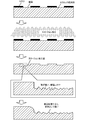
- the upper surface of the ceramic sintered body is mirror-finished, the portion where the convex portion is to be formed is covered with a mask, and the portion not covered by the mask is crushed by erosion processing. Is common (see FIG. 2).
- the present invention has been made to solve such a problem, and a main object thereof is to prevent the generation of particles in a semiconductor process.
- the wafer mounting table of the present invention A wafer mounting table having a plurality of protrusions on the surface of a ceramic sintered body to support a wafer.
- the portion of the surface of the ceramic sintered body without the convex portion is a mirror surface having a surface roughness Ra of 0.1 ⁇ m or less.
- the convex portion is an aerosol deposition (AD) film or a thermal sprayed film made of the same material as the ceramic sintered body. It is a thing.
- This wafer mounting table can be obtained, for example, by mirror-finishing the surface of the ceramic sintered body and then forming an AD film or a thermal sprayed film at a portion where a convex portion is desired to be formed. Since the portion of the surface of the ceramic sintered body of the wafer mounting table without the convex portion is a mirror surface, it does not cause the generation of particles. Therefore, according to this wafer mounting table, it is possible to prevent the generation of particles in the semiconductor process.
- the convex portion may have rounded corners (boundary between the top surface and the side surface). In this way, the corner of the convex portion is unlikely to be a stress concentration point with respect to the mechanical external force.
- the convex portion may be less dense than the ceramic sintered body.
- the ceramic sintered body can be made dense by adopting hot press firing or the like.
- the convex portion is an AD film or a thermal sprayed film, the density is lower than that of the ceramic sintered body.
- the manufacturing method of the wafer mounting table of the present invention is (A) A process of mirror-finishing the surface of the ceramic sintered body and (B) A step of forming a convex portion on the portion of the surface on which the convex portion is desired to be formed by an AD method or a thermal spraying method. Is included.
- the wafer mounting table of the present invention described above can be manufactured relatively easily.
- the manufacturing process diagram of the wafer mounting table of this embodiment A manufacturing process diagram of a conventional wafer mounting table.
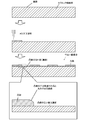
- FIG. 1 is a manufacturing process diagram (vertical cross-sectional view) of the wafer mounting table of the present embodiment.
- the wafer mounting table is provided with a plurality of convex portions that support the wafer on the surface of the disk-shaped ceramic sintered body.
- the portion of the surface of the ceramic sintered body having no convex portion is a mirror surface having a surface roughness Ra of 0.1 ⁇ m or less.
- the convex portion is an AD film or a thermal sprayed film made of the same material as the ceramic sintered body.
- the corners of the convex portion (the boundary between the top surface and the side surface) are rounded in cross section. Looking at the cross section of the wafer mounting table, the convex portion has a lower density than the ceramic sintered body.
- the ceramic sintered body is made dense by adopting hot press firing.
- the convex portion is an AD film or a thermal sprayed film
- the density is lower than that of the ceramic sintered body (for example, the porosity is high).
- the ceramic sintered body may include at least one of an electrostatic electrode, an RF electrode, and a heater electrode (resistive heating element).
- the top surface of the convex portion may be polished.
- the wafer mounting table is manufactured by (a) a step of mirror-finishing the surface of the ceramic sintered body and (b) an AD method (including a plasma AD method) or a thermal spraying method on the portion of the surface where a convex portion is desired to be formed. It includes a step of forming a convex portion.
- the surface may be covered with a mask so that only the portion of the surface on which the convex portion is to be formed is exposed, and the convex portion may be formed on the exposed portion by the AD method or the thermal spraying method. Since the AD method can form ceramic particles by the impact solidification phenomenon, it is not necessary to sinter the ceramic particles at a high temperature.
- the convex portion is formed of an AD film rather than a sprayed film. This is because the AD film is relatively dense and has high adhesion to the surface.
- the convex portion is formed by the thermal spraying method, it is preferable to roughen the portion where the convex portion is to be formed in order to improve the adhesion.
- the portion of the surface of the ceramic sintered body having no convex portion is a mirror surface, it does not cause the generation of particles. Therefore, according to this wafer mounting table, it is possible to prevent the generation of particles in the semiconductor process.
- the present invention can be used for, for example, film forming processes such as semiconductor wafer transfer, exposure, and CVD, and microfabrication such as cleaning, etching, and dicing.
Landscapes
- Engineering & Computer Science (AREA)
- Chemical & Material Sciences (AREA)
- Physics & Mathematics (AREA)
- Plasma & Fusion (AREA)
- Mechanical Engineering (AREA)
- Chemical Kinetics & Catalysis (AREA)
- Materials Engineering (AREA)
- Metallurgy (AREA)
- Organic Chemistry (AREA)
- Container, Conveyance, Adherence, Positioning, Of Wafer (AREA)
Abstract
Description
セラミック焼結体の表面にウエハを支持する複数の凸部を備えたウエハ載置台であって、
前記セラミック焼結体の前記表面のうち前記凸部のない部分は、表面粗さRaが0.1μm以下の鏡面であり、
前記凸部は、前記セラミック焼結体と同じ材質のエアロゾルデポジション(AD)膜又は溶射膜である、
ものである。
(a)セラミック焼結体の表面を鏡面仕上げする工程と、
(b)前記表面のうち凸部を形成したい部分にAD法又は溶射法により凸部を形成する工程と、
を含むものである。
Claims (4)
- セラミック焼結体の表面にウエハを支持する複数の凸部を備えたウエハ載置台であって、
前記セラミック焼結体の前記表面のうち前記凸部のない部分は、表面粗さRaが0.1μm以下の鏡面であり、
前記凸部は、前記セラミック焼結体と同じ材質のエアロゾルデポジション膜又は溶射膜である、
ウエハ載置台。 - 前記凸部は、角が丸みを帯びている、
請求項1に記載のウエハ載置台。 - 前記凸部は、前記セラミック焼結体に比べて緻密性が低い、
請求項1又は2に記載のウエハ載置台。 - (a)セラミック焼結体の表面を鏡面仕上げする工程と、
(b)前記表面のうち凸部を形成したい部分にエアロゾルデポジション法又は溶射法により凸部を形成する工程と、
を含むウエハ載置台の製法。
Priority Applications (4)
| Application Number | Priority Date | Filing Date | Title |
|---|---|---|---|
| KR1020217040469A KR102672383B1 (ko) | 2019-06-28 | 2020-06-10 | 웨이퍼 배치대 및 그 제법 |
| CN202080047761.6A CN114072901A (zh) | 2019-06-28 | 2020-06-10 | 晶片载置台及其制法 |
| JP2021528133A JP7284261B2 (ja) | 2019-06-28 | 2020-06-10 | ウエハ載置台及びその製法 |
| US17/643,600 US12087613B2 (en) | 2019-06-28 | 2021-12-10 | Wafer placement table and method of manufacturing the same |
Applications Claiming Priority (2)
| Application Number | Priority Date | Filing Date | Title |
|---|---|---|---|
| JP2019121487 | 2019-06-28 | ||
| JP2019-121487 | 2019-06-28 |
Related Child Applications (1)
| Application Number | Title | Priority Date | Filing Date |
|---|---|---|---|
| US17/643,600 Continuation US12087613B2 (en) | 2019-06-28 | 2021-12-10 | Wafer placement table and method of manufacturing the same |
Publications (1)
| Publication Number | Publication Date |
|---|---|
| WO2020261990A1 true WO2020261990A1 (ja) | 2020-12-30 |
Family
ID=74059855
Family Applications (1)
| Application Number | Title | Priority Date | Filing Date |
|---|---|---|---|
| PCT/JP2020/022830 Ceased WO2020261990A1 (ja) | 2019-06-28 | 2020-06-10 | ウエハ載置台及びその製法 |
Country Status (5)
| Country | Link |
|---|---|
| US (1) | US12087613B2 (ja) |
| JP (1) | JP7284261B2 (ja) |
| KR (1) | KR102672383B1 (ja) |
| CN (1) | CN114072901A (ja) |
| WO (1) | WO2020261990A1 (ja) |
Cited By (1)
| Publication number | Priority date | Publication date | Assignee | Title |
|---|---|---|---|---|
| WO2026009814A1 (ja) * | 2024-07-02 | 2026-01-08 | 日本碍子株式会社 | ウエハ載置台 |
Families Citing this family (1)
| Publication number | Priority date | Publication date | Assignee | Title |
|---|---|---|---|---|
| JP7284261B2 (ja) * | 2019-06-28 | 2023-05-30 | 日本碍子株式会社 | ウエハ載置台及びその製法 |
Citations (4)
| Publication number | Priority date | Publication date | Assignee | Title |
|---|---|---|---|---|
| JP2005033221A (ja) * | 2001-02-08 | 2005-02-03 | Tokyo Electron Ltd | 基板載置台および処理装置 |
| JP2011100844A (ja) * | 2009-11-05 | 2011-05-19 | Shin-Etsu Chemical Co Ltd | 静電吸着機能を有する装置及びその製造方法 |
| JP2015023168A (ja) * | 2013-07-19 | 2015-02-02 | 株式会社日立ハイテクノロジーズ | プラズマ処理装置、及びステージ製造方法 |
| JP2018536287A (ja) * | 2015-11-17 | 2018-12-06 | アプライド マテリアルズ インコーポレイテッドApplied Materials,Incorporated | 堆積された表面フィーチャを有する基板支持アセンブリ |
Family Cites Families (21)
| Publication number | Priority date | Publication date | Assignee | Title |
|---|---|---|---|---|
| JPH083191A (ja) * | 1994-06-15 | 1996-01-09 | Kuraray Co Ltd | 抗血栓性ペプチドおよびこれを固定化した医療用具 |
| US20050260930A1 (en) * | 1999-06-15 | 2005-11-24 | Yuji Okuda | Table of wafer of polishing apparatus, method for polishing semiconductor wafer, and method for manufacturing semiconductor wafer |
| US7040963B1 (en) * | 1999-06-15 | 2006-05-09 | Ibiden Co., Ltd. | Table of wafer polishing apparatus, method for polishing semiconductor wafer, and method for manufacturing semiconductor wafer |
| US8545583B2 (en) * | 2000-11-17 | 2013-10-01 | Wayne O. Duescher | Method of forming a flexible abrasive sheet article |
| US8062098B2 (en) * | 2000-11-17 | 2011-11-22 | Duescher Wayne O | High speed flat lapping platen |
| JP3626933B2 (ja) | 2001-02-08 | 2005-03-09 | 東京エレクトロン株式会社 | 基板載置台の製造方法 |
| US20030047283A1 (en) * | 2001-09-10 | 2003-03-13 | Applied Materials, Inc. | Apparatus for supporting a substrate and method of fabricating same |
| US7070480B2 (en) * | 2001-10-11 | 2006-07-04 | Applied Materials, Inc. | Method and apparatus for polishing substrates |
| JP2006147724A (ja) | 2004-11-17 | 2006-06-08 | Ngk Insulators Ltd | 静電チャック及びその製造方法 |
| JP2006147834A (ja) * | 2004-11-19 | 2006-06-08 | Nec Schott Components Corp | 気密端子およびそれを用いた薄型金属パッケージ |
| JP2006287210A (ja) * | 2005-03-07 | 2006-10-19 | Ngk Insulators Ltd | 静電チャック及びその製造方法 |
| JP2007109827A (ja) * | 2005-10-12 | 2007-04-26 | Toto Ltd | 静電チャック |
| JP5059450B2 (ja) * | 2007-03-06 | 2012-10-24 | 東京エレクトロン株式会社 | 基板載置台及び基板処理装置 |
| CN101870086A (zh) * | 2009-04-27 | 2010-10-27 | 三菱综合材料株式会社 | Cmp修整器及其制造方法 |
| JP5510411B2 (ja) * | 2010-08-11 | 2014-06-04 | Toto株式会社 | 静電チャック及び静電チャックの製造方法 |
| KR101806413B1 (ko) * | 2014-09-29 | 2017-12-07 | 주식회사 엘지화학 | 막 증착장치 및 이를 이용한 열전소자 제조방법 |
| KR101916872B1 (ko) * | 2015-10-15 | 2018-11-08 | 아이원스 주식회사 | 반도체 공정 장비 부품의 코팅층 재생 방법 및 이에 따른 반도체 공정 장비 부품 |
| WO2019087977A1 (ja) * | 2017-10-30 | 2019-05-09 | 日本碍子株式会社 | 静電チャック及びその製法 |
| JP6627936B1 (ja) * | 2018-08-30 | 2020-01-08 | 住友大阪セメント株式会社 | 静電チャック装置および静電チャック装置の製造方法 |
| CN111668148B (zh) * | 2019-03-05 | 2024-09-03 | Toto株式会社 | 静电吸盘及处理装置 |
| JP7284261B2 (ja) * | 2019-06-28 | 2023-05-30 | 日本碍子株式会社 | ウエハ載置台及びその製法 |
-
2020
- 2020-06-10 JP JP2021528133A patent/JP7284261B2/ja active Active
- 2020-06-10 KR KR1020217040469A patent/KR102672383B1/ko active Active
- 2020-06-10 CN CN202080047761.6A patent/CN114072901A/zh active Pending
- 2020-06-10 WO PCT/JP2020/022830 patent/WO2020261990A1/ja not_active Ceased
-
2021
- 2021-12-10 US US17/643,600 patent/US12087613B2/en active Active
Patent Citations (4)
| Publication number | Priority date | Publication date | Assignee | Title |
|---|---|---|---|---|
| JP2005033221A (ja) * | 2001-02-08 | 2005-02-03 | Tokyo Electron Ltd | 基板載置台および処理装置 |
| JP2011100844A (ja) * | 2009-11-05 | 2011-05-19 | Shin-Etsu Chemical Co Ltd | 静電吸着機能を有する装置及びその製造方法 |
| JP2015023168A (ja) * | 2013-07-19 | 2015-02-02 | 株式会社日立ハイテクノロジーズ | プラズマ処理装置、及びステージ製造方法 |
| JP2018536287A (ja) * | 2015-11-17 | 2018-12-06 | アプライド マテリアルズ インコーポレイテッドApplied Materials,Incorporated | 堆積された表面フィーチャを有する基板支持アセンブリ |
Cited By (2)
| Publication number | Priority date | Publication date | Assignee | Title |
|---|---|---|---|---|
| WO2026009814A1 (ja) * | 2024-07-02 | 2026-01-08 | 日本碍子株式会社 | ウエハ載置台 |
| WO2026009813A1 (ja) * | 2024-07-02 | 2026-01-08 | 日本碍子株式会社 | ウエハ載置台 |
Also Published As
| Publication number | Publication date |
|---|---|
| JPWO2020261990A1 (ja) | 2020-12-30 |
| US20220102186A1 (en) | 2022-03-31 |
| JP7284261B2 (ja) | 2023-05-30 |
| KR102672383B1 (ko) | 2024-06-04 |
| KR20220006617A (ko) | 2022-01-17 |
| CN114072901A (zh) | 2022-02-18 |
| US12087613B2 (en) | 2024-09-10 |
Similar Documents
| Publication | Publication Date | Title |
|---|---|---|
| KR102338223B1 (ko) | 정전 척 장치 | |
| JP6443504B2 (ja) | 静電チャック装置 | |
| TWI809980B (zh) | 具有沉積表面特徵之基板支撐組件 | |
| JP5293211B2 (ja) | 静電チャックおよび静電チャックの製造方法 | |
| JP6380177B2 (ja) | 静電チャック装置 | |
| JP4782744B2 (ja) | 吸着部材、吸着装置および吸着方法 | |
| JP6867149B2 (ja) | 基板保持部材 | |
| KR20140033436A (ko) | 정전기 척 aln 유전체 수리 | |
| JP5515365B2 (ja) | 静電チャックおよび静電チャックの製造方法 | |
| JP7214867B2 (ja) | 静電チャック | |
| JP4739039B2 (ja) | 静電チャック装置 | |
| JP7376594B2 (ja) | シャフト付きセラミックヒータ | |
| JP5453902B2 (ja) | 静電チャックおよび静電チャックの製造方法 | |
| JP2018014515A (ja) | 静電チャック及びその製造方法並びに静電チャックの再生方法 | |
| JP2018006573A (ja) | 静電チャック及びその製造方法並びに静電チャックの再生方法 | |
| US12087613B2 (en) | Wafer placement table and method of manufacturing the same | |
| JP7096031B2 (ja) | 基板保持部材 | |
| JP6782157B2 (ja) | 静電チャック | |
| CN114026957A (zh) | 带轴的陶瓷加热器 | |
| JP4159029B2 (ja) | セラミックス製プレート | |
| JPH0536818A (ja) | ウエハチヤツク | |
| JP2004046046A (ja) | 液晶基板加熱用炭素製治具 |
Legal Events
| Date | Code | Title | Description |
|---|---|---|---|
| 121 | Ep: the epo has been informed by wipo that ep was designated in this application |
Ref document number: 20832049 Country of ref document: EP Kind code of ref document: A1 |
|
| ENP | Entry into the national phase |
Ref document number: 2021528133 Country of ref document: JP Kind code of ref document: A |
|
| ENP | Entry into the national phase |
Ref document number: 20217040469 Country of ref document: KR Kind code of ref document: A |
|
| NENP | Non-entry into the national phase |
Ref country code: DE |
|
| 122 | Ep: pct application non-entry in european phase |
Ref document number: 20832049 Country of ref document: EP Kind code of ref document: A1 |