WO2020217404A1 - ドルメン構造を有する半導体装置及びその製造方法 - Google Patents
ドルメン構造を有する半導体装置及びその製造方法 Download PDFInfo
- Publication number
- WO2020217404A1 WO2020217404A1 PCT/JP2019/017713 JP2019017713W WO2020217404A1 WO 2020217404 A1 WO2020217404 A1 WO 2020217404A1 JP 2019017713 W JP2019017713 W JP 2019017713W WO 2020217404 A1 WO2020217404 A1 WO 2020217404A1
- Authority
- WO
- WIPO (PCT)
- Prior art keywords
- chip
- adhesive
- piece
- support piece
- film
- Prior art date
- Legal status (The legal status is an assumption and is not a legal conclusion. Google has not performed a legal analysis and makes no representation as to the accuracy of the status listed.)
- Ceased
Links
Images






Classifications
-
- H—ELECTRICITY
- H10—SEMICONDUCTOR DEVICES; ELECTRIC SOLID-STATE DEVICES NOT OTHERWISE PROVIDED FOR
- H10W—GENERIC PACKAGES, INTERCONNECTIONS, CONNECTORS OR OTHER CONSTRUCTIONAL DETAILS OF DEVICES COVERED BY CLASS H10
- H10W42/00—Arrangements for protection of devices
- H10W42/121—Arrangements for protection of devices protecting against mechanical damage
-
- H—ELECTRICITY
- H10—SEMICONDUCTOR DEVICES; ELECTRIC SOLID-STATE DEVICES NOT OTHERWISE PROVIDED FOR
- H10W—GENERIC PACKAGES, INTERCONNECTIONS, CONNECTORS OR OTHER CONSTRUCTIONAL DETAILS OF DEVICES COVERED BY CLASS H10
- H10W72/00—Interconnections or connectors in packages
- H10W72/30—Die-attach connectors
-
- H—ELECTRICITY
- H10—SEMICONDUCTOR DEVICES; ELECTRIC SOLID-STATE DEVICES NOT OTHERWISE PROVIDED FOR
- H10W—GENERIC PACKAGES, INTERCONNECTIONS, CONNECTORS OR OTHER CONSTRUCTIONAL DETAILS OF DEVICES COVERED BY CLASS H10
- H10W72/00—Interconnections or connectors in packages
- H10W72/851—Dispositions of multiple connectors or interconnections
-
- H—ELECTRICITY
- H10—SEMICONDUCTOR DEVICES; ELECTRIC SOLID-STATE DEVICES NOT OTHERWISE PROVIDED FOR
- H10W—GENERIC PACKAGES, INTERCONNECTIONS, CONNECTORS OR OTHER CONSTRUCTIONAL DETAILS OF DEVICES COVERED BY CLASS H10
- H10W90/00—Package configurations
-
- H—ELECTRICITY
- H10—SEMICONDUCTOR DEVICES; ELECTRIC SOLID-STATE DEVICES NOT OTHERWISE PROVIDED FOR
- H10W—GENERIC PACKAGES, INTERCONNECTIONS, CONNECTORS OR OTHER CONSTRUCTIONAL DETAILS OF DEVICES COVERED BY CLASS H10
- H10W99/00—Subject matter not provided for in other groups of this subclass
-
- H—ELECTRICITY
- H10—SEMICONDUCTOR DEVICES; ELECTRIC SOLID-STATE DEVICES NOT OTHERWISE PROVIDED FOR
- H10W—GENERIC PACKAGES, INTERCONNECTIONS, CONNECTORS OR OTHER CONSTRUCTIONAL DETAILS OF DEVICES COVERED BY CLASS H10
- H10W72/00—Interconnections or connectors in packages
- H10W72/071—Connecting or disconnecting
- H10W72/073—Connecting or disconnecting of die-attach connectors
-
- H—ELECTRICITY
- H10—SEMICONDUCTOR DEVICES; ELECTRIC SOLID-STATE DEVICES NOT OTHERWISE PROVIDED FOR
- H10W—GENERIC PACKAGES, INTERCONNECTIONS, CONNECTORS OR OTHER CONSTRUCTIONAL DETAILS OF DEVICES COVERED BY CLASS H10
- H10W72/00—Interconnections or connectors in packages
- H10W72/071—Connecting or disconnecting
- H10W72/073—Connecting or disconnecting of die-attach connectors
- H10W72/07321—Aligning
- H10W72/07327—Aligning involving guiding structures, e.g. spacers or supporting members
-
- H—ELECTRICITY
- H10—SEMICONDUCTOR DEVICES; ELECTRIC SOLID-STATE DEVICES NOT OTHERWISE PROVIDED FOR
- H10W—GENERIC PACKAGES, INTERCONNECTIONS, CONNECTORS OR OTHER CONSTRUCTIONAL DETAILS OF DEVICES COVERED BY CLASS H10
- H10W72/00—Interconnections or connectors in packages
- H10W72/071—Connecting or disconnecting
- H10W72/073—Connecting or disconnecting of die-attach connectors
- H10W72/07331—Connecting techniques
- H10W72/07337—Connecting techniques using a polymer adhesive, e.g. an adhesive based on silicone or epoxy
- H10W72/07338—Connecting techniques using a polymer adhesive, e.g. an adhesive based on silicone or epoxy hardening the adhesive by curing, e.g. thermosetting
-
- H—ELECTRICITY
- H10—SEMICONDUCTOR DEVICES; ELECTRIC SOLID-STATE DEVICES NOT OTHERWISE PROVIDED FOR
- H10W—GENERIC PACKAGES, INTERCONNECTIONS, CONNECTORS OR OTHER CONSTRUCTIONAL DETAILS OF DEVICES COVERED BY CLASS H10
- H10W72/00—Interconnections or connectors in packages
- H10W72/071—Connecting or disconnecting
- H10W72/075—Connecting or disconnecting of bond wires
-
- H—ELECTRICITY
- H10—SEMICONDUCTOR DEVICES; ELECTRIC SOLID-STATE DEVICES NOT OTHERWISE PROVIDED FOR
- H10W—GENERIC PACKAGES, INTERCONNECTIONS, CONNECTORS OR OTHER CONSTRUCTIONAL DETAILS OF DEVICES COVERED BY CLASS H10
- H10W72/00—Interconnections or connectors in packages
- H10W72/30—Die-attach connectors
- H10W72/351—Materials of die-attach connectors
- H10W72/353—Materials of die-attach connectors not comprising solid metals or solid metalloids, e.g. ceramics
- H10W72/354—Materials of die-attach connectors not comprising solid metals or solid metalloids, e.g. ceramics comprising polymers
-
- H—ELECTRICITY
- H10—SEMICONDUCTOR DEVICES; ELECTRIC SOLID-STATE DEVICES NOT OTHERWISE PROVIDED FOR
- H10W—GENERIC PACKAGES, INTERCONNECTIONS, CONNECTORS OR OTHER CONSTRUCTIONAL DETAILS OF DEVICES COVERED BY CLASS H10
- H10W72/00—Interconnections or connectors in packages
- H10W72/50—Bond wires
- H10W72/551—Materials of bond wires
-
- H—ELECTRICITY
- H10—SEMICONDUCTOR DEVICES; ELECTRIC SOLID-STATE DEVICES NOT OTHERWISE PROVIDED FOR
- H10W—GENERIC PACKAGES, INTERCONNECTIONS, CONNECTORS OR OTHER CONSTRUCTIONAL DETAILS OF DEVICES COVERED BY CLASS H10
- H10W72/00—Interconnections or connectors in packages
- H10W72/851—Dispositions of multiple connectors or interconnections
- H10W72/874—On different surfaces
- H10W72/884—Die-attach connectors and bond wires
-
- H—ELECTRICITY
- H10—SEMICONDUCTOR DEVICES; ELECTRIC SOLID-STATE DEVICES NOT OTHERWISE PROVIDED FOR
- H10W—GENERIC PACKAGES, INTERCONNECTIONS, CONNECTORS OR OTHER CONSTRUCTIONAL DETAILS OF DEVICES COVERED BY CLASS H10
- H10W72/00—Interconnections or connectors in packages
- H10W72/90—Bond pads, in general
- H10W72/931—Shapes of bond pads
-
- H—ELECTRICITY
- H10—SEMICONDUCTOR DEVICES; ELECTRIC SOLID-STATE DEVICES NOT OTHERWISE PROVIDED FOR
- H10W—GENERIC PACKAGES, INTERCONNECTIONS, CONNECTORS OR OTHER CONSTRUCTIONAL DETAILS OF DEVICES COVERED BY CLASS H10
- H10W72/00—Interconnections or connectors in packages
- H10W72/90—Bond pads, in general
- H10W72/951—Materials of bond pads
-
- H—ELECTRICITY
- H10—SEMICONDUCTOR DEVICES; ELECTRIC SOLID-STATE DEVICES NOT OTHERWISE PROVIDED FOR
- H10W—GENERIC PACKAGES, INTERCONNECTIONS, CONNECTORS OR OTHER CONSTRUCTIONAL DETAILS OF DEVICES COVERED BY CLASS H10
- H10W72/00—Interconnections or connectors in packages
- H10W72/90—Bond pads, in general
- H10W72/951—Materials of bond pads
- H10W72/952—Materials of bond pads comprising metals or metalloids, e.g. PbSn, Ag or Cu
-
- H—ELECTRICITY
- H10—SEMICONDUCTOR DEVICES; ELECTRIC SOLID-STATE DEVICES NOT OTHERWISE PROVIDED FOR
- H10W—GENERIC PACKAGES, INTERCONNECTIONS, CONNECTORS OR OTHER CONSTRUCTIONAL DETAILS OF DEVICES COVERED BY CLASS H10
- H10W72/00—Interconnections or connectors in packages
- H10W72/90—Bond pads, in general
- H10W72/951—Materials of bond pads
- H10W72/953—Materials of bond pads not comprising solid metals or solid metalloids, e.g. polymers, ceramics or liquids
-
- H—ELECTRICITY
- H10—SEMICONDUCTOR DEVICES; ELECTRIC SOLID-STATE DEVICES NOT OTHERWISE PROVIDED FOR
- H10W—GENERIC PACKAGES, INTERCONNECTIONS, CONNECTORS OR OTHER CONSTRUCTIONAL DETAILS OF DEVICES COVERED BY CLASS H10
- H10W74/00—Encapsulations, e.g. protective coatings
-
- H—ELECTRICITY
- H10—SEMICONDUCTOR DEVICES; ELECTRIC SOLID-STATE DEVICES NOT OTHERWISE PROVIDED FOR
- H10W—GENERIC PACKAGES, INTERCONNECTIONS, CONNECTORS OR OTHER CONSTRUCTIONAL DETAILS OF DEVICES COVERED BY CLASS H10
- H10W74/00—Encapsulations, e.g. protective coatings
- H10W74/10—Encapsulations, e.g. protective coatings characterised by their shape or disposition
- H10W74/111—Encapsulations, e.g. protective coatings characterised by their shape or disposition the semiconductor body being completely enclosed
- H10W74/114—Encapsulations, e.g. protective coatings characterised by their shape or disposition the semiconductor body being completely enclosed by a substrate and the encapsulations
-
- H—ELECTRICITY
- H10—SEMICONDUCTOR DEVICES; ELECTRIC SOLID-STATE DEVICES NOT OTHERWISE PROVIDED FOR
- H10W—GENERIC PACKAGES, INTERCONNECTIONS, CONNECTORS OR OTHER CONSTRUCTIONAL DETAILS OF DEVICES COVERED BY CLASS H10
- H10W90/00—Package configurations
- H10W90/20—Configurations of stacked chips
- H10W90/24—Configurations of stacked chips at least one of the stacked chips being laterally offset from a neighbouring stacked chip, e.g. chip stacks having a staircase shape
-
- H—ELECTRICITY
- H10—SEMICONDUCTOR DEVICES; ELECTRIC SOLID-STATE DEVICES NOT OTHERWISE PROVIDED FOR
- H10W—GENERIC PACKAGES, INTERCONNECTIONS, CONNECTORS OR OTHER CONSTRUCTIONAL DETAILS OF DEVICES COVERED BY CLASS H10
- H10W90/00—Package configurations
- H10W90/701—Package configurations characterised by the relative positions of pads or connectors relative to package parts
- H10W90/731—Package configurations characterised by the relative positions of pads or connectors relative to package parts of die-attach connectors
- H10W90/732—Package configurations characterised by the relative positions of pads or connectors relative to package parts of die-attach connectors between stacked chips
-
- H—ELECTRICITY
- H10—SEMICONDUCTOR DEVICES; ELECTRIC SOLID-STATE DEVICES NOT OTHERWISE PROVIDED FOR
- H10W—GENERIC PACKAGES, INTERCONNECTIONS, CONNECTORS OR OTHER CONSTRUCTIONAL DETAILS OF DEVICES COVERED BY CLASS H10
- H10W90/00—Package configurations
- H10W90/701—Package configurations characterised by the relative positions of pads or connectors relative to package parts
- H10W90/731—Package configurations characterised by the relative positions of pads or connectors relative to package parts of die-attach connectors
- H10W90/734—Package configurations characterised by the relative positions of pads or connectors relative to package parts of die-attach connectors between a chip and a stacked insulating package substrate, interposer or RDL
-
- H—ELECTRICITY
- H10—SEMICONDUCTOR DEVICES; ELECTRIC SOLID-STATE DEVICES NOT OTHERWISE PROVIDED FOR
- H10W—GENERIC PACKAGES, INTERCONNECTIONS, CONNECTORS OR OTHER CONSTRUCTIONAL DETAILS OF DEVICES COVERED BY CLASS H10
- H10W90/00—Package configurations
- H10W90/701—Package configurations characterised by the relative positions of pads or connectors relative to package parts
- H10W90/751—Package configurations characterised by the relative positions of pads or connectors relative to package parts of bond wires
- H10W90/754—Package configurations characterised by the relative positions of pads or connectors relative to package parts of bond wires between a chip and a stacked insulating package substrate, interposer or RDL
Definitions
- the present disclosure is supported and first by a substrate, a first chip arranged on the substrate, a plurality of support pieces arranged on the substrate and around the first chip, and a plurality of support pieces.
- the present invention relates to a semiconductor device having a dolmen structure including a second chip arranged so as to cover the chip.
- the present disclosure also relates to a method for manufacturing a semiconductor device having a dolmen structure.
- a dolmen (dolmen) is a kind of stone tomb, and has a plurality of pillar stones and a plate-shaped rock placed on the pillar stone.
- a support piece corresponds to a "dolmen"
- a second chip corresponds to a "plate-shaped rock".
- Patent Document 1 discloses a semiconductor die assembly including a controller die and a memory die supported by a support member on the controller die. It can be said that the semiconductor assembly 100 illustrated in FIG. 1A of Patent Document 1 has a dolmen structure.
- the semiconductor assembly 100 includes the package substrate 102, the controller dies 103 arranged on the surface of the package substrate 102, the memory dies 106a and 106b arranged above the controller dies 103, and the support members 130a and 130b for supporting the memory dies 106a. To be equipped.
- Patent Document 1 discloses that a semiconductor material such as silicon can be used as a support member (support piece), and more specifically, a fragment of the semiconductor material obtained by dicing a semiconductor wafer can be used (Patent Document 1). 1 [0012], [0014] and FIG. 2). In order to manufacture a support piece for a dolmen structure using a semiconductor wafer, for example, the following steps are required as in the case of manufacturing a normal semiconductor chip.
- Step of attaching back grind tape to semiconductor wafer (2) Step of back grinding semiconductor wafer (3) Adhesive layer and adhesive layer for dicing ring and semiconductor wafer after back grind placed in it Step of pasting a film (dicing / die bonding integrated film) with and (4) Step of peeling back grind tape from semiconductor wafer (5) Step of fragmenting semiconductor wafer (6) Semiconductor chip and adhesive piece A process of picking up a support piece made of a laminated body from an adhesive layer
- the present disclosure provides a method for manufacturing a semiconductor device, which can simplify the step of manufacturing a support piece in the manufacturing process of a semiconductor device having a dolmen structure, and further can stably support a laminated semiconductor chip. ..
- the present disclosure also provides a semiconductor device having a dolmen structure.
- One aspect of the present disclosure relates to a method for manufacturing a semiconductor device having a dolmen structure.
- This manufacturing method includes the following steps.
- a step of forming a plurality of support pieces on the surface of the adhesive layer (C) a step of picking up the support pieces from the adhesive layer (D) a step of arranging the first chip on the substrate (E) on the substrate.
- Step of arranging a plurality of support pieces around the first chip (F) Prepare a chip with an adhesive piece including the second chip and the adhesive piece provided on one surface of the second chip.
- a support piece obtained by individualizing a support piece forming film is used.
- the step of manufacturing the support piece can be simplified as compared with the conventional manufacturing method in which a fragment of the semiconductor material obtained by dicing a semiconductor wafer is used as the support piece. That is, while the above-mentioned steps (1) to (6) have been conventionally required, since the support piece forming film does not include the semiconductor wafer, the back grind of the semiconductor wafer (1), (2) and The step (4) can be omitted.
- the thermosetting resin layer has adhesiveness to other members (for example, a substrate), it is not necessary to separately provide an adhesive layer or the like on the support piece.
- the support piece forming film is obtained by thermocompression bonding the support piece forming film to the adhesive piece of the chip with an adhesive piece and curing the support piece forming film at 170 ° C. for 1 hour, and then the support piece (support piece).
- the shear strength of the cured product of the forming film) and the chip with the adhesive piece at 250 ° C. is 3.2 MPa or more.
- a support piece formed from such a support piece forming film tends to have a higher share strength than a conventional support piece using a fragment of a semiconductor material obtained by dicing a semiconductor wafer. The reason for this is considered, for example, that the film for forming the support piece and the adhesive piece are cured products of the resin.
- the adhesive layer of the laminated film prepared in the step (A) may be a pressure-sensitive type or an ultraviolet curable type. That is, the adhesive layer may or may not be cured by ultraviolet irradiation, in other words, it may or may not contain a resin having a carbon-carbon double bond having photoreactivity. It does not have to be.
- the pressure-sensitive adhesive layer may contain a resin having a carbon-carbon double bond having photoreactivity.
- the adhesive layer may be one in which the adhesiveness of the predetermined region is lowered by irradiating the predetermined region with ultraviolet rays, and for example, a resin having a carbon-carbon double bond having photoreactivity may be used. It may remain.
- the adhesive layer is an ultraviolet curable type, the adhesiveness of the adhesive layer can be reduced by carrying out a step of irradiating the adhesive layer with ultraviolet rays between the steps (B) and (C).
- the support piece forming film has at least a thermosetting resin layer.
- the step of heating the support piece forming film or the support piece to cure the thermosetting resin layer or the adhesive piece may be carried out at an appropriate timing, and may be carried out, for example, before the step (G).
- the thermosetting resin layer is already cured to prevent the support pieces from being deformed with the arrangement of the chips with adhesive pieces. it can.
- the support piece forming film may be any one of the following films.
- -A film composed of a thermosetting resin layer-A three-layer film having a thermosetting resin layer, a resin layer having higher rigidity than the thermosetting resin layer, and a thermosetting resin layer-The thermosetting resin layer A three-layer film having a metal layer having a higher rigidity than the thermosetting resin layer and a thermosetting resin layer.
- the rigidity of the thermosetting resin layer after thermosetting is that of the resin layer or the metal layer. It may be lower or higher than the rigidity. Rigidity means the ability of an object to withstand fracture against bending or twisting.
- One aspect of this disclosure relates to a semiconductor device having a dolmen structure. That is, the semiconductor device is supported by the substrate, the first chip arranged on the substrate, the plurality of support pieces arranged on the substrate and around the first chip, and the plurality of support pieces. Includes an adhesive insert chip arranged to cover the first chip, and the adhesive insert insert comprises and supports an adhesive insert provided on one surface of the second chip and the second chip.
- the share strength of the piece and the tip with the adhesive piece at 250 ° C. is 3.2 MPa or more.
- the share strength between the support piece and the chip with adhesive piece at 250 ° C. is 3.2 MPa or more, the chip with adhesive piece can be stably supported by the support piece, and the connection reliability in the semiconductor device can be maintained for a long period of time. Can be secured.
- the support piece may be any one of the following. -Composed of a cured product of a thermosetting resin composition-A product having a layer of a cured product of a thermosetting resin composition, a resin layer, and a layer of a cured product of a thermosetting resin composition-The thermosetting property Those having a layer of a cured product of a resin composition, a metal layer, and a layer of a cured product of a thermosetting resin composition.
- the semiconductor device includes an adhesive piece provided on one surface of the second chip and sandwiched between the second chip and a plurality of support pieces.
- the first chip may be separated from the adhesive piece or may be in contact with the adhesive piece.
- a method for manufacturing a semiconductor device capable of simplifying the step of manufacturing a support piece and stably supporting a laminated semiconductor chip is provided.
- the present disclosure also provides a semiconductor device having a dolmen structure.
- FIG. 1 is a cross-sectional view schematically showing a first embodiment of a semiconductor device.
- 2 (a), 2 (b), and 2 (c) are plan views schematically showing an example of the positional relationship between the first chip and the plurality of support pieces.
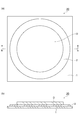
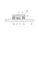
- FIG. 3A is a plan view schematically showing an embodiment of a laminated film for forming a support piece
- FIG. 3B is a cross-sectional view taken along the line bb of FIG. 3A.
- FIG. 4 is a cross-sectional view schematically showing a step of bonding the adhesive layer and the support piece forming film.
- 5 (a), 5 (b), 5 (c), and 5 (d) are cross-sectional views schematically showing the manufacturing process of the support piece.
- FIG. 1 is a cross-sectional view schematically showing a first embodiment of a semiconductor device.
- 2 (a), 2 (b), and 2 (c) are plan views schematically showing an example of the positional relationship between the first chip and the plurality of support pieces
- FIG. 6 is a cross-sectional view schematically showing a state in which a plurality of support pieces are arranged on the substrate and around the first chip.
- FIG. 7 is a cross-sectional view schematically showing an example of a chip with an adhesive piece.
- FIG. 8 is a cross-sectional view schematically showing a dolmen structure formed on the substrate.
- FIG. 9 is a cross-sectional view schematically showing a second embodiment of the semiconductor device.
- FIG. 10 is a cross-sectional view schematically showing another embodiment of the laminated film for forming a support piece.
- (meth) acrylic acid means acrylic acid or methacrylic acid
- (meth) acrylate means acrylate or the corresponding methacrylate
- a or B may include either A or B, or both.
- the term “layer” includes not only a structure having a shape formed on the entire surface but also a structure having a shape partially formed when observed as a plan view.
- the term “process” is used not only as an independent process but also as a term as long as the desired action of the process is achieved even when it cannot be clearly distinguished from other processes. included.
- the numerical range indicated by using "-” indicates a range including the numerical values before and after "-" as the minimum value and the maximum value, respectively.
- the content of each component in the composition is the total amount of the plurality of substances present in the composition unless otherwise specified, when a plurality of substances corresponding to each component are present in the composition.
- the exemplary materials may be used alone or in combination of two or more unless otherwise specified.
- the upper limit value or the lower limit value of the numerical range of one step may be replaced with the upper limit value or the lower limit value of the numerical range of another step.
- the upper limit value or the lower limit value of the numerical range may be replaced with the value shown in the examples.
- FIG. 1 is a cross-sectional view schematically showing a first embodiment of a semiconductor device.
- the semiconductor device 100 shown in FIG. 1 includes a substrate 10, a chip T1 (first chip) arranged on the surface of the substrate 10, and a plurality of chips T1 (first chip) arranged on the surface of the substrate 10 and around the chip T1.
- a plurality of wires w for electrically connecting the electrodes (not shown) on the surface of the 10 and the chips T1 to T4, respectively, and a sealing material 50 filled in a gap between the chips T1 and the chips T2 and the like are provided.
- the tip T2c with an adhesive piece includes an adhesive piece Tc provided on one surface of the tip T2 (second tip) and the tip T2 (second tip).
- a dolmen structure is formed on the substrate 10 by a plurality of support pieces Dc and a chip T2c with an adhesive piece.
- the chip T1 is separated from the adhesive piece Tc.
- the substrate 10 may be an organic substrate or a metal substrate such as a lead frame. From the viewpoint of suppressing the warp of the semiconductor device 100, the thickness of the substrate 10 is, for example, 90 to 300 ⁇ m, and may be 90 to 210 ⁇ m.
- the chip T1 is, for example, a controller chip, which is adhered to the substrate 10 by an adhesive piece Tc and electrically connected to the substrate 10 by a wire w.
- the shape of the chip T1 in a plan view is, for example, a rectangle (square or rectangle).
- the length of one side of the chip T1 is, for example, 5 mm or less, and may be 2 to 5 mm or 1 to 5 mm.
- the thickness of the chip T1 is, for example, 10 to 150 ⁇ m, and may be 20 to 100 ⁇ m.
- the chip T2 is, for example, a memory chip, and is adhered onto the support piece Dc via the adhesive piece Tc. In plan view, the chip T2 has a larger size than the chip T1.
- the shape of the chip T2 in a plan view is, for example, a rectangle (square or rectangle).
- the length of one side of the chip T2 is, for example, 20 mm or less, and may be 4 to 20 mm or 4 to 12 mm.
- the thickness of the chip T2 is, for example, 10 to 170 ⁇ m, and may be 20 to 120 ⁇ m.
- the chips T3 and T4 are also memory chips, for example, and are adhered onto the chip T2 via an adhesive piece Tc.
- the length of one side of the chips T3 and T4 may be the same as that of the chip T2, and the thickness of the chips T3 and T4 may be the same as that of the chip T2.
- the support piece Dc acts as a spacer that forms a space around the chip T1.
- the support piece Dc is a cured product of a thermosetting resin composition (a cured product of a film composed of a thermosetting resin layer).
- a thermosetting resin composition a cured product of a film composed of a thermosetting resin layer.
- two support pieces Dc shape: rectangle
- One support piece Dc shape: square, 4 in total
- One support piece Dc may be arranged at a position corresponding to the corner of the chip T1, or as shown in FIG. 2C, a position corresponding to the side of the chip T1.
- One support piece Dc shape: rectangle, total of 4 pieces
- the length of one side of the support piece Dc in a plan view is, for example, 20 mm or less, and may be 1 to 20 mm or 1 to 12 mm.
- the thickness (height) of the support piece Dc is, for example, 10 to 180 ⁇ m, and may be 20 to 120 ⁇ m.
- the share strength of the support piece Dc and the tip T2c with the adhesive piece at 250 ° C. is 3.2 MPa or more, and may be 3.3 MPa or more, 3.4 MPa or more, or 3.5 MPa or more.
- the support piece Dc can stably support the adhesive chip T2c, and the connection reliability in the semiconductor device can be achieved. Can be secured for a long period of time.
- the upper limit of the share strength of the support piece Dc and the chip T2c with the adhesive piece at 250 ° C. is not particularly limited, but may be 10 MPa or less.
- the support piece Dc shown in FIG. 1 is after the thermosetting tree composition has been cured.
- the support piece Da is in a state before the thermosetting tree composition is completely cured (see, for example, FIG. 5B).
- the laminated film 20 for forming a support piece (hereinafter, sometimes referred to as "laminated film 20") shown in FIGS. 3 (a) and 3 (b) is prepared.
- the laminated film 20 includes a base film 1, an adhesive layer 2, and a support piece forming film D having at least a thermosetting resin layer.
- the base film 1 is, for example, a polyethylene terephthalate film (PET film).
- PET film polyethylene terephthalate film
- the adhesive layer 2 is formed in a circular shape by punching or the like (see FIG. 3A).
- the adhesive layer 2 is made of an ultraviolet curable adhesive. That is, the adhesive layer 2 has a property that the adhesiveness is lowered by being irradiated with ultraviolet rays.
- the support piece forming film D is formed in a circular shape by punching or the like, and has a diameter smaller than that of the adhesive layer 2 (see FIG. 3A).
- the support piece forming film D has at least a thermosetting resin layer 5 made of a thermosetting resin composition.
- thermosetting resin composition constituting the thermosetting resin layer 5 in the support piece forming film D can be in a completely cured product (C stage) state by a semi-curing (B stage) state and then a curing treatment. Is.
- the thermosetting resin composition when the support piece is formed, the share strength of the support piece and the chip with the adhesive piece at 250 ° C. can be easily adjusted within a predetermined range. Therefore, the epoxy resin, the curing agent, and the elastomer (for example, it may contain an acrylic resin) and, if necessary, an inorganic filler, a curing accelerator, or the like. Details of the thermosetting resin composition constituting the thermosetting resin layer 5 in the support piece forming film D will be described later.
- the thickness of the support piece forming film D may be, for example, 5 to 180 ⁇ m or 20 to 120 ⁇ m.
- a dolmen structure having an appropriate height with respect to the first chip (for example, a controller chip) can be constructed.
- the support piece forming film D is obtained by thermocompression-bonding the adhesive piece Tc of the chip T2c with an adhesive piece to the support piece forming film D and curing the support piece forming film D at 170 ° C. for 1 hour.
- the share strength of Dc (a cured product of the film D for forming a support piece) and the chip T2c with an adhesive piece at 250 ° C. is 3.2 MPa or more.
- the share strength of the support piece Dc (cured product of the film D for forming the support piece) and the chip T2c with the adhesive piece at 250 ° C. may be 3.3 MPa or more, 3.4 MPa or more, or 3.5 MPa or more.
- the upper limit of the share strength of the support piece Dc (the cured product of the film D for forming the support piece) and the chip T2c with the adhesive piece at 250 ° C. is not particularly limited, but may be, for example, 10 MPa or less.
- the laminated film 20 is, for example, a second laminated film having a base film 1 and an adhesive layer 2 on the surface thereof, and a cover film 3 and a support piece forming film D on the surface thereof. It can be produced by laminating with a film (see FIG. 4).
- the first laminated film is obtained through a step of forming an adhesive layer on the surface of the base film 1 by coating and a step of processing the adhesive layer into a predetermined shape (for example, a circle) by punching or the like.
- the second laminated film has a step of forming a support piece forming film on the surface of the cover film 3 (for example, PET film or polyethylene film) by coating, and a predetermined shape (for example, by punching the support piece forming film). For example, it is obtained through a process of processing into a circular shape.
- the cover film 3 is peeled off at an appropriate timing.
- the dicing ring DR is attached to the laminated film 20. That is, the dicing ring DR is attached to the adhesive layer 2 of the laminated film 20, and the support piece forming film D is arranged inside the dicing ring DR.
- the support piece forming film D is individualized by dicing (see FIG. 5B). As a result, a large number of support pieces Da can be obtained from the support piece forming film D.
- the adhesive layer 2 is irradiated with ultraviolet rays to reduce the adhesive force between the adhesive layer 2 and the support piece Da.
- the base film 1 is expanded to separate the support pieces Da from each other. As shown in FIG.
- the support piece Da is peeled off from the adhesive layer 2 by pushing up the support piece Da with the push-up jig 42, and the support piece Da is picked up by suction with the suction collet 44.
- the curing reaction of the thermosetting resin may be allowed to proceed by heating the support piece forming film D before dicing or the support piece Da before picking up. Excellent pickup performance can be achieved by appropriately curing the support piece Da when picking up.
- the manufacturing method according to this embodiment includes the following steps (A) to (H).
- E Step of arranging a plurality of support pieces Da on the substrate 10 around the first chip T1 (see FIG. 6).
- (F) A step of preparing a chip T2a with an adhesive piece, which includes a second chip T2 and an adhesive piece Ta provided on one surface of the second chip T2 (see FIG. 7).
- (G) A step of constructing a dolmen structure by arranging a chip T2a with an adhesive piece on the surface of a plurality of support pieces Dc (see FIG. 8).
- (H) A step of sealing the gap between the chip T1 and the chip T2 with the sealing material 50 (see FIG. 1).
- the steps (A) to (C) are processes for producing a plurality of support pieces Da, and have already been described.
- the steps (D) to (H) are processes in which a dolmen structure is constructed on the substrate 10 by using a plurality of support pieces Da.
- the steps (D) to (H) will be described with reference to FIGS. 6 to 8.
- the step (D) is a step of arranging the first chip T1 on the substrate 10. For example, first, the chip T1 is arranged at a predetermined position on the substrate 10 via the adhesive layer T1c. After that, the chip T1 is electrically connected to the substrate 10 by the wire w.
- the step (E) is a step of arranging a plurality of support pieces Da on the substrate 10 around the first chip T1.
- the structure 30 shown in FIG. 6 is produced.
- the structure 30 includes a substrate 10, a chip T1 arranged on the surface thereof, and a plurality of support pieces Da.
- the support piece Da may be arranged by crimping.
- the crimping treatment is preferably carried out, for example, under the conditions of 80 to 180 ° C. and 0.01 to 0.50 MPa for 0.5 to 3.0 seconds.
- the support piece Da may be completely cured at the time of the step (E) to become the support piece Dc, and may not be completely cured at this time. It is preferable that the support piece Da is completely cured to become the support piece Dc before the start of the step (G).
- the step (F) is a step of preparing the adhesive chip T2a shown in FIG. 7.
- the adhesive piece T2a includes a chip T2 and an adhesive piece Ta provided on the surface of one of the chips T2.
- the chip T2a with an adhesive piece can be obtained through a dicing step and a pick-up step using, for example, a semiconductor wafer and a dicing / die bonding integrated film.
- the step (G) is a step of arranging the chip T2a with the adhesive piece above the chip T1 so that the adhesive piece Ta is in contact with the upper surface of the plurality of support pieces Dc.
- the chip T2 is crimped to the upper surface of the support piece Dc via the adhesive piece Ta.
- This crimping treatment is preferably carried out for 0.5 to 3.0 seconds under the conditions of, for example, 80 to 180 ° C. and 0.01 to 0.50 MPa.
- the adhesive piece Ta is cured by heating. This curing treatment is preferably carried out for 5 minutes or more under the conditions of, for example, 60 to 175 ° C. and 0.01 to 1.0 MPa. As a result, the adhesive piece Ta is cured to become the adhesive piece Tc.
- a dolmen structure is constructed on the substrate 10 (see FIG. 8).
- the chip T3 is placed on the chip T2 via the adhesive piece, and further, the chip T4 is placed on the chip T3 via the adhesive piece.
- the adhesive piece may be any thermosetting resin composition similar to the above-mentioned adhesive piece Ta, and becomes an adhesive piece Tc by heat curing (see FIG. 1).
- the chips T2, T3 and T4 and the substrate 10 are electrically connected by wires w.
- the number of chips stacked above the chip T1 is not limited to the three in this embodiment, and may be appropriately set.
- Step (H) The step (H) is a step of sealing the gap between the chip T1 and the chip T2 with the sealing material 50. Through this step, the semiconductor device 100 shown in FIG. 1 is completed.
- the support piece forming film D has at least a thermosetting resin layer 5.
- the thermosetting resin composition constituting the thermosetting resin layer 5 in the support piece forming film D has a share strength at 250 ° C. between the support piece and the chip with the adhesive piece when the support piece is formed. Since it is easy to adjust to a predetermined range, it may contain an epoxy resin, a curing agent, an elastomer, and if necessary, an inorganic filler, a curing accelerator, or the like. According to the studies by the present inventors, it is preferable that the support piece Da and the hardened support piece Dc further have the following characteristics.
- -Characteristic 1 The adhesive strength of the chip T2c with the adhesive piece to the adhesive piece Tc is sufficiently high.
- -Characteristic 2 When the support piece Da is thermocompression bonded to a predetermined position on the substrate 10, misalignment is unlikely to occur (120).
- the melt viscosity (shear viscosity) of the adhesive piece 5p at ° C. is, for example, 4300 to 50,000 Pa ⁇ s or 5000 to 40,000 Pa ⁇ s).
- -Characteristic 3 The adhesive piece 5c exhibits stress relaxation property in the semiconductor device 100 (the thermosetting resin composition contains an elastomer (rubber component)).
- -Characteristic 4 The shrinkage rate due to curing is sufficiently small.
- -Characteristic 5 The visibility of the support piece Da by the camera in the pickup process is good (the thermosetting resin composition contains, for example, a colorant).
- -Characteristic 6 The adhesive piece 5c has sufficient mechanical strength.
- Epoxy resin The epoxy resin is not particularly limited as long as it is cured and has an adhesive action.
- Bifunctional epoxy resins such as bisphenol A type epoxy resin, bisphenol F type epoxy resin, and bisphenol S type epoxy resin, novolak type epoxy resins such as phenol novolac type epoxy resin and cresol novolac type epoxy resin can be used.
- novolak type epoxy resins such as phenol novolac type epoxy resin and cresol novolac type epoxy resin
- generally known ones such as a polyfunctional epoxy resin, a glycidylamine type epoxy resin, a heterocyclic epoxy resin, and an alicyclic epoxy resin can be applied. These may be used alone or in combination of two or more.
- Examples of the curing agent include phenolic resins, ester compounds, aromatic amines, aliphatic amines, acid anhydrides and the like. Of these, phenolic resins are preferable from the viewpoint of achieving high share strength (die share strength).
- Commercially available phenolic resins include, for example, LF-4871 (trade name, BPA novolac type phenolic resin) manufactured by DIC Corporation and HE-100C-30 (trade name, phenylarakil type phenol) manufactured by Air Water Inc.
- the blending amount of the epoxy resin and the phenol resin is preferably such that the equivalent ratio of the epoxy equivalent and the hydroxyl group equivalent is 0.6 to 1.5, and 0.7 to 0.7, respectively, from the viewpoint of achieving a high share strength (die share strength). It is more preferably 1.4, and even more preferably 0.8 to 1.3. When the compounding ratio is within the above range, both curability and fluidity can be easily achieved at a sufficiently high level.
- Examples of the elastoma include acrylic resin, polyester resin, polyamide resin, polyimide resin, silicone resin, polybutadiene, acrylonitrile, epoxy-modified polybutadiene, maleic anhydride-modified polybutadiene, phenol-modified polybutadiene, and carboxy-modified acrylonitrile.
- an acrylic resin is preferable as the elastoma, and a functional monomer having an epoxy group such as glycidyl acrylate or glycidyl methacrylate or a glycidyl group as a crosslinkable functional group is polymerized.
- Acrylic resins such as epoxy group-containing (meth) acrylic copolymers are more preferable.
- epoxy group-containing (meth) acrylic acid ester copolymers and epoxy group-containing acrylic rubbers are preferable, and epoxy group-containing acrylic rubbers are more preferable.
- the epoxy group-containing acrylic rubber is a rubber having an epoxy group, which is mainly composed of an acrylic acid ester as a main component, a copolymer such as butyl acrylate and acrylonitrile, and a copolymer such as ethyl acrylate and acrylonitrile.
- the acrylic resin may have not only an epoxy group but also a crosslinkable functional group such as an alcoholic or phenolic hydroxyl group or a carboxyl group.
- acrylic resin products examples include SG-70L, SG-708-6, WS-023 EK30, SG-280 EK23, and SG-P3 solvent-modified products manufactured by Nagase Chemtech Co., Ltd. (trade name, acrylic rubber, Weight average molecular weight: 800,000, Tg: 12 ° C., solvent is cyclohexanone) and the like.
- the glass transition temperature (Tg) of the acrylic resin is preferably ⁇ 50 to 50 ° C., more preferably ⁇ 30 to 30 ° C., from the viewpoint of achieving high shear strength (die shear strength).
- the weight average molecular weight (Mw) of the acrylic resin is preferably 100,000 to 3 million, more preferably 500,000 to 2 million, from the viewpoint of achieving high share strength (die share strength).
- Mw means a value measured by gel permeation chromatography (GPC) and converted using a calibration curve using standard polystyrene.
- the amount of acrylic resin contained in the thermosetting resin composition is 10 to 200 parts by mass with respect to 100 parts by mass in total of the epoxy resin and the epoxy resin curing agent from the viewpoint of achieving high shear strength (die shear strength). It is preferably 20 to 100 parts by mass, and more preferably 20 to 100 parts by mass.
- inorganic filler examples include aluminum hydroxide, magnesium hydroxide, calcium carbonate, magnesium carbonate, calcium silicate, magnesium silicate, calcium oxide, magnesium oxide, aluminum oxide, aluminum nitride, aluminum borate whisker, boron nitride, and crystals. Examples thereof include sex silica and amorphous silica. These may be used alone or in combination of two or more.
- the average particle size of the inorganic filler is preferably 0.005 ⁇ m to 1.0 ⁇ m, more preferably 0.05 to 0.5 ⁇ m, from the viewpoint of achieving high shear strength (die shear strength).
- the surface of the inorganic filler is preferably chemically modified from the viewpoint of achieving high shear strength (die shear strength).
- Examples of the material that chemically modifies the surface include a silane coupling agent and the like.
- the functional group of the silane coupling agent include a vinyl group, an acryloyl group, an epoxy group, a mercapto group, an amino group, a diamino group, an alkoxy group, an ethoxy group and the like.
- the content of the inorganic filler is preferably 20 to 200 parts by mass, preferably 30 to 100 parts by mass, based on 100 parts by mass of the resin component of the thermosetting resin composition. It is more preferable that it is a part.
- curing accelerator examples include imidazoles and derivatives thereof, organophosphorus compounds, secondary amines, tertiary amines, quaternary ammonium salts and the like. From the viewpoint of achieving high shear strength (die shear strength), imidazole-based compounds are preferable.
- imidazoles include 2-methylimidazole, 1-benzyl-2-methylimidazole, 1-cyanoethyl-2-phenylimidazole, 1-cyanoethyl-2-methylimidazole and the like. These may be used alone or in combination of two or more.
- the content of the curing accelerator in the thermosetting resin composition is 0.04 to 3 parts by mass with respect to 100 parts by mass of the total of the epoxy resin and the epoxy resin curing agent from the viewpoint of achieving high shear strength (die shear strength). Is preferable, and 0.04 to 0.2 parts by mass is more preferable.
- FIG. 9 is a cross-sectional view schematically showing a second embodiment of the semiconductor device.
- the chip T1 is separated from the adhesive piece Tc, whereas in the semiconductor device 200 according to the present embodiment, the chip T1 is in contact with the adhesive piece Tc. That is, the adhesive piece Tc is in contact with the upper surface of the chip T1 and the upper surface of the support piece Dc.
- the thickness of the support piece forming film D the position of the upper surface of the chip T1 and the position of the upper surface of the support piece Dc can be matched.
- the chip T1 is connected to the substrate 10 by a flip chip instead of wire bonding. If the chip T2 is embedded in the adhesive piece Ta constituting the adhesive piece T2a together with the chip T2, the chip T1 is in contact with the adhesive piece Tc even in the mode in which the chip T1 is wire-bonded to the substrate 10. Can be in the state of
- a support piece forming laminated film 20 including a support piece forming film D having a single layer structure is illustrated, but there are three support piece forming laminated films. It may be a layer.
- the laminated film 20A for forming a support piece shown in FIG. 10 includes a thermosetting resin layer 5, a resin layer 6 or a metal layer having higher rigidity than the thermosetting resin layer, and a thermosetting resin layer 5. It has a three-layer film D2 (a film for forming a support piece) which is held in order.
- the laminated film 20A for forming a support piece can be manufactured, for example, through the following steps. -A step of preparing a laminated film including a base film 1, an adhesive layer 2, and a thermosetting resin layer 5 in this order.-A resin having a higher rigidity than the thermosetting resin layer 5 on the surface of the laminated film. Step of laminating layer 6 or metal layer-Step of laminating a thermosetting resin layer 5 on the surface of resin layer 6 or metal layer
- Varnish A was filtered through a 100 mesh filter and vacuum defoamed.
- a polyethylene terephthalate (PET) film having been subjected to a mold release treatment having a thickness of 38 ⁇ m was prepared, and varnish A after vacuum defoaming was applied onto the PET film.
- the applied varnish A was heat-dried at 90 ° C. for 5 minutes and then at 130 ° C. for 5 minutes in two steps to obtain a support piece forming film of Production Example 1 in the B stage state.
- the amount of varnish A applied was adjusted so that the thickness was 50 ⁇ m.
- a dicing / die-bonding integrated adhesive film (film-like adhesive: thickness 50 ⁇ m, adhesive film: thickness 110 ⁇ m, manufactured by Hitachi Kasei Co., Ltd.) and a silicon wafer having a thickness of 400 ⁇ m, which include a film-like adhesive and an adhesive film.
- a dicing sample was prepared by laminating a silicon wafer on a film-like adhesive of a dicing / die bonding integrated adhesive film at a stage temperature of 70 ° C.
- the obtained dicing sample was cut using a fully automatic dicer DFD-6361 (manufactured by Disco Corporation).
- the cutting was performed by a step cutting method using two blades, and dicing blades ZH05-SD3500-N1-xx-DD and ZH05-SD4000-N1-xx-BB (both manufactured by Disco Corporation) were used.
- the cutting conditions were a blade rotation speed of 4000 rpm, a cutting speed of 50 mm / sec, and a chip size of 5 mm ⁇ 5 mm.
- the first step was cut so that the silicon wafer remained about 200 ⁇ m, and then the second step was cut so that the adhesive film had a notch of about 20 ⁇ m.
- the tip was picked up using a pick-up collet to obtain a tip with an adhesive piece.
- Example 1 A solder resist substrate (Taiyo Holdings Co., Ltd., trade name: AUS-308) and a support piece forming film of Production Example 1 are prepared, and the solder resist substrate is applied to the support piece forming film of Production Example 1 at a stage temperature of 70 ° C. Laminated. Next, the adhesive piece-attached chip produced above was prepared, and one side of the adhesive piece of the adhesive piece-attached chip was placed on the support piece forming film of Production Example 1 and thermocompression bonded. The thermocompression bonding conditions were a temperature of 120 ° C., a time of 1 second, and a pressure of 0.1 MPa. Subsequently, the sample obtained by thermocompression bonding was placed in a dryer and cured at 170 ° C. for 1 hour to prepare an evaluation sample of Example 1.
- Example 2 An evaluation sample of Example 2 was prepared in the same manner as in Example 1 except that the support piece forming film of Production Example 1 was changed to the support piece forming film of Production Example 2.
- Example 3 An evaluation sample of Example 3 was prepared in the same manner as in Example 1 except that the support piece forming film of Production Example 1 was changed to the support piece forming film of Production Example 3.
- thermocompression bonding conditions were a temperature of 120 ° C., a time of 1 second, and a pressure of 0.1 MPa. Subsequently, the sample obtained by thermocompression bonding was placed in a dryer and cured at 170 ° C. for 1 hour to prepare an evaluation sample of Comparative Example 1.
- a method for manufacturing a semiconductor device capable of simplifying the step of manufacturing a support piece and stably supporting a laminated semiconductor chip is provided.
- the present disclosure also provides a semiconductor device having a dolmen structure.
Landscapes
- Die Bonding (AREA)
- Adhesives Or Adhesive Processes (AREA)
- Adhesive Tapes (AREA)
- Engineering & Computer Science (AREA)
- Manufacturing & Machinery (AREA)
- Dicing (AREA)
Priority Applications (7)
| Application Number | Priority Date | Filing Date | Title |
|---|---|---|---|
| JP2021515423A JP7294410B2 (ja) | 2019-04-25 | 2019-04-25 | ドルメン構造を有する半導体装置及びその製造方法 |
| PCT/JP2019/017713 WO2020217404A1 (ja) | 2019-04-25 | 2019-04-25 | ドルメン構造を有する半導体装置及びその製造方法 |
| CN201980094137.9A CN113574663B (zh) | 2019-04-25 | 2019-04-25 | 具有支石墓结构的半导体装置及其制造方法 |
| KR1020217029577A KR102711424B1 (ko) | 2019-04-25 | 2019-04-25 | 돌멘 구조를 갖는 반도체 장치 및 그 제조 방법 |
| SG11202110111YA SG11202110111YA (en) | 2019-04-25 | 2019-04-25 | Semiconductor device having dolmen structure and method for manufacturing same |
| US17/438,943 US12412880B2 (en) | 2019-04-25 | 2019-04-25 | Semiconductor device having dolmen structure and method for manufacturing same |
| TW109112888A TWI830901B (zh) | 2019-04-25 | 2020-04-17 | 半導體裝置的製造方法 |
Applications Claiming Priority (1)
| Application Number | Priority Date | Filing Date | Title |
|---|---|---|---|
| PCT/JP2019/017713 WO2020217404A1 (ja) | 2019-04-25 | 2019-04-25 | ドルメン構造を有する半導体装置及びその製造方法 |
Publications (1)
| Publication Number | Publication Date |
|---|---|
| WO2020217404A1 true WO2020217404A1 (ja) | 2020-10-29 |
Family
ID=72941128
Family Applications (1)
| Application Number | Title | Priority Date | Filing Date |
|---|---|---|---|
| PCT/JP2019/017713 Ceased WO2020217404A1 (ja) | 2019-04-25 | 2019-04-25 | ドルメン構造を有する半導体装置及びその製造方法 |
Country Status (7)
| Country | Link |
|---|---|
| US (1) | US12412880B2 (https=) |
| JP (1) | JP7294410B2 (https=) |
| KR (1) | KR102711424B1 (https=) |
| CN (1) | CN113574663B (https=) |
| SG (1) | SG11202110111YA (https=) |
| TW (1) | TWI830901B (https=) |
| WO (1) | WO2020217404A1 (https=) |
Cited By (3)
| Publication number | Priority date | Publication date | Assignee | Title |
|---|---|---|---|---|
| KR20240136990A (ko) | 2022-01-12 | 2024-09-19 | 가부시끼가이샤 레조낙 | 개편화체 형성용 적층 필름 및 그 제조 방법, 및 반도체 장치의 제조 방법 |
| WO2025023100A1 (ja) * | 2023-07-21 | 2025-01-30 | 株式会社レゾナック | 半導体装置及び半導体装置の製造方法 |
| WO2025164537A1 (ja) * | 2024-02-02 | 2025-08-07 | 株式会社レゾナック | 個片化体形成用積層フィルム及び半導体装置の製造方法 |
Families Citing this family (3)
| Publication number | Priority date | Publication date | Assignee | Title |
|---|---|---|---|---|
| WO2020217394A1 (ja) * | 2019-04-25 | 2020-10-29 | 日立化成株式会社 | ドルメン構造を有する半導体装置及びその製造方法、並びに、支持片形成用積層フィルム及びその製造方法 |
| WO2020217404A1 (ja) | 2019-04-25 | 2020-10-29 | 日立化成株式会社 | ドルメン構造を有する半導体装置及びその製造方法 |
| JP7452545B2 (ja) * | 2019-08-29 | 2024-03-19 | 株式会社レゾナック | 支持片の製造方法、半導体装置の製造方法、及び支持片形成用積層フィルム |
Citations (12)
| Publication number | Priority date | Publication date | Assignee | Title |
|---|---|---|---|---|
| JP2002222889A (ja) * | 2001-01-24 | 2002-08-09 | Nec Kyushu Ltd | 半導体装置及びその製造方法 |
| JP2003124433A (ja) * | 2001-08-27 | 2003-04-25 | Samsung Electronics Co Ltd | マルチチップパッケージ |
| JP2006005333A (ja) * | 2004-05-20 | 2006-01-05 | Toshiba Corp | 積層型電子部品とその製造方法 |
| US20070181990A1 (en) * | 2006-02-03 | 2007-08-09 | Siliconware Precision Industries Co., Ltd. | Stacked semiconductor structure and fabrication method thereof |
| US20080029885A1 (en) * | 2006-08-07 | 2008-02-07 | Sandisk Il Ltd. | Inverted Pyramid Multi-Die Package Reducing Wire Sweep And Weakening Torques |
| US7859119B1 (en) * | 2003-11-10 | 2010-12-28 | Amkor Technology, Inc. | Stacked flip chip die assembly |
| JP2013127014A (ja) * | 2011-12-16 | 2013-06-27 | Hitachi Chemical Co Ltd | 接着シート |
| JP2013131557A (ja) * | 2011-12-20 | 2013-07-04 | Toshiba Corp | 半導体装置およびその製造方法 |
| US20130270717A1 (en) * | 2012-04-17 | 2013-10-17 | Samsung Electronics Co., Ltd. | Semiconductor package and method of fabricating the same |
| JP2015176906A (ja) * | 2014-03-13 | 2015-10-05 | 株式会社東芝 | 半導体装置および半導体装置の製造方法 |
| JP2016021585A (ja) * | 2012-03-08 | 2016-02-04 | 日立化成株式会社 | 接着シート及び半導体装置の製造方法 |
| JP2017515306A (ja) * | 2014-04-29 | 2017-06-08 | マイクロン テクノロジー, インク. | 支持部材を有する積層半導体ダイアセンブリと、関連するシステムおよび方法 |
Family Cites Families (28)
| Publication number | Priority date | Publication date | Assignee | Title |
|---|---|---|---|---|
| JP3210126B2 (ja) | 1993-03-15 | 2001-09-17 | 株式会社東芝 | 液晶表示装置の製造方法 |
| US5721452A (en) | 1995-08-16 | 1998-02-24 | Micron Technology, Inc. | Angularly offset stacked die multichip device and method of manufacture |
| US6787916B2 (en) * | 2001-09-13 | 2004-09-07 | Tru-Si Technologies, Inc. | Structures having a substrate with a cavity and having an integrated circuit bonded to a contact pad located in the cavity |
| DE10360708B4 (de) | 2003-12-19 | 2008-04-10 | Infineon Technologies Ag | Halbleitermodul mit einem Halbleiterstapel, Umverdrahtungsplatte, und Verfahren zur Herstellung derselben |
| US7312261B2 (en) * | 2004-05-11 | 2007-12-25 | International Business Machines Corporation | Thermal interface adhesive and rework |
| US7064430B2 (en) * | 2004-08-31 | 2006-06-20 | Stats Chippac Ltd. | Stacked die packaging and fabrication method |
| JP4954569B2 (ja) * | 2006-02-16 | 2012-06-20 | 日東電工株式会社 | 半導体装置の製造方法 |
| WO2007109326A2 (en) * | 2006-03-21 | 2007-09-27 | Promerus Llc | Methods and materials useful for chip stacking, chip and wafer bonding |
| TWI317993B (en) | 2006-08-18 | 2009-12-01 | Advanced Semiconductor Eng | Stackable semiconductor package |
| JP2010040835A (ja) * | 2008-08-06 | 2010-02-18 | Toshiba Corp | 積層型半導体装置の製造方法 |
| JP5791866B2 (ja) | 2009-03-06 | 2015-10-07 | 株式会社ディスコ | ワーク分割装置 |
| JPWO2010110069A1 (ja) | 2009-03-23 | 2012-09-27 | 日立化成工業株式会社 | ダイボンディング用樹脂ペースト、それを用いた半導体装置の製造方法、及び半導体装置 |
| US8169058B2 (en) | 2009-08-21 | 2012-05-01 | Stats Chippac, Ltd. | Semiconductor device and method of stacking die on leadframe electrically connected by conductive pillars |
| KR20120080634A (ko) * | 2009-11-13 | 2012-07-17 | 히다치 가세고교 가부시끼가이샤 | 반도체 장치, 반도체 장치의 제조 방법 및 접착제층 부착 반도체 웨이퍼 |
| KR20110083969A (ko) * | 2010-01-15 | 2011-07-21 | 삼성전자주식회사 | 반도체 패키지 및 그 제조 방법 |
| JP4976522B2 (ja) | 2010-04-16 | 2012-07-18 | 日東電工株式会社 | 熱硬化型ダイボンドフィルム、ダイシング・ダイボンドフィルム、及び、半導体装置の製造方法 |
| JP5013148B1 (ja) | 2011-02-16 | 2012-08-29 | 株式会社東京精密 | ワーク分割装置及びワーク分割方法 |
| KR101774938B1 (ko) * | 2011-08-31 | 2017-09-06 | 삼성전자 주식회사 | 지지대를 갖는 반도체 패키지 및 그 형성 방법 |
| JP5537515B2 (ja) * | 2011-09-01 | 2014-07-02 | 株式会社東芝 | 積層型半導体装置の製造方法と製造装置 |
| CN105143380B (zh) | 2013-03-28 | 2019-05-17 | 古河电气工业株式会社 | 粘合带及晶片加工用胶带 |
| KR102161776B1 (ko) | 2014-03-28 | 2020-10-06 | 에스케이하이닉스 주식회사 | 적층 패키지 |
| US9412722B1 (en) | 2015-02-12 | 2016-08-09 | Dawning Leading Technology Inc. | Multichip stacking package structure and method for manufacturing the same |
| DE102015204698B4 (de) * | 2015-03-16 | 2023-07-20 | Disco Corporation | Verfahren zum Teilen eines Wafers |
| JP6603479B2 (ja) | 2015-05-18 | 2019-11-06 | 日東電工株式会社 | 接着フィルム、ダイシングテープ一体型接着フィルム、複層フィルム、半導体装置の製造方法および半導体装置 |
| US10297575B2 (en) * | 2016-05-06 | 2019-05-21 | Amkor Technology, Inc. | Semiconductor device utilizing an adhesive to attach an upper package to a lower die |
| WO2018159305A1 (ja) | 2017-02-28 | 2018-09-07 | パナソニックIpマネジメント株式会社 | ピラー供給用シートの製造方法、ガラスパネルユニットの製造方法及びガラス窓の製造方法 |
| WO2020217404A1 (ja) | 2019-04-25 | 2020-10-29 | 日立化成株式会社 | ドルメン構造を有する半導体装置及びその製造方法 |
| IT201900006736A1 (it) | 2019-05-10 | 2020-11-10 | Applied Materials Inc | Procedimenti di fabbricazione di package |
-
2019
- 2019-04-25 WO PCT/JP2019/017713 patent/WO2020217404A1/ja not_active Ceased
- 2019-04-25 JP JP2021515423A patent/JP7294410B2/ja active Active
- 2019-04-25 CN CN201980094137.9A patent/CN113574663B/zh active Active
- 2019-04-25 KR KR1020217029577A patent/KR102711424B1/ko active Active
- 2019-04-25 US US17/438,943 patent/US12412880B2/en active Active
- 2019-04-25 SG SG11202110111YA patent/SG11202110111YA/en unknown
-
2020
- 2020-04-17 TW TW109112888A patent/TWI830901B/zh active
Patent Citations (12)
| Publication number | Priority date | Publication date | Assignee | Title |
|---|---|---|---|---|
| JP2002222889A (ja) * | 2001-01-24 | 2002-08-09 | Nec Kyushu Ltd | 半導体装置及びその製造方法 |
| JP2003124433A (ja) * | 2001-08-27 | 2003-04-25 | Samsung Electronics Co Ltd | マルチチップパッケージ |
| US7859119B1 (en) * | 2003-11-10 | 2010-12-28 | Amkor Technology, Inc. | Stacked flip chip die assembly |
| JP2006005333A (ja) * | 2004-05-20 | 2006-01-05 | Toshiba Corp | 積層型電子部品とその製造方法 |
| US20070181990A1 (en) * | 2006-02-03 | 2007-08-09 | Siliconware Precision Industries Co., Ltd. | Stacked semiconductor structure and fabrication method thereof |
| US20080029885A1 (en) * | 2006-08-07 | 2008-02-07 | Sandisk Il Ltd. | Inverted Pyramid Multi-Die Package Reducing Wire Sweep And Weakening Torques |
| JP2013127014A (ja) * | 2011-12-16 | 2013-06-27 | Hitachi Chemical Co Ltd | 接着シート |
| JP2013131557A (ja) * | 2011-12-20 | 2013-07-04 | Toshiba Corp | 半導体装置およびその製造方法 |
| JP2016021585A (ja) * | 2012-03-08 | 2016-02-04 | 日立化成株式会社 | 接着シート及び半導体装置の製造方法 |
| US20130270717A1 (en) * | 2012-04-17 | 2013-10-17 | Samsung Electronics Co., Ltd. | Semiconductor package and method of fabricating the same |
| JP2015176906A (ja) * | 2014-03-13 | 2015-10-05 | 株式会社東芝 | 半導体装置および半導体装置の製造方法 |
| JP2017515306A (ja) * | 2014-04-29 | 2017-06-08 | マイクロン テクノロジー, インク. | 支持部材を有する積層半導体ダイアセンブリと、関連するシステムおよび方法 |
Cited By (3)
| Publication number | Priority date | Publication date | Assignee | Title |
|---|---|---|---|---|
| KR20240136990A (ko) | 2022-01-12 | 2024-09-19 | 가부시끼가이샤 레조낙 | 개편화체 형성용 적층 필름 및 그 제조 방법, 및 반도체 장치의 제조 방법 |
| WO2025023100A1 (ja) * | 2023-07-21 | 2025-01-30 | 株式会社レゾナック | 半導体装置及び半導体装置の製造方法 |
| WO2025164537A1 (ja) * | 2024-02-02 | 2025-08-07 | 株式会社レゾナック | 個片化体形成用積層フィルム及び半導体装置の製造方法 |
Also Published As
| Publication number | Publication date |
|---|---|
| KR102711424B1 (ko) | 2024-09-26 |
| CN113574663B (zh) | 2025-12-12 |
| SG11202110111YA (en) | 2021-11-29 |
| JP7294410B2 (ja) | 2023-06-20 |
| CN113574663A (zh) | 2021-10-29 |
| TW202044423A (zh) | 2020-12-01 |
| KR20210145737A (ko) | 2021-12-02 |
| TWI830901B (zh) | 2024-02-01 |
| JPWO2020217404A1 (https=) | 2020-10-29 |
| US12412880B2 (en) | 2025-09-09 |
| US20220157802A1 (en) | 2022-05-19 |
Similar Documents
| Publication | Publication Date | Title |
|---|---|---|
| JP7294410B2 (ja) | ドルメン構造を有する半導体装置及びその製造方法 | |
| WO2020100998A1 (ja) | 半導体装置及びその製造方法、並びに半導体装置の製造に使用される構造体 | |
| JP7494841B2 (ja) | ドルメン構造を有する半導体装置及びその製造方法、並びに、支持片形成用積層フィルム及びその製造方法 | |
| JP7247733B2 (ja) | ドルメン構造を有する半導体装置の製造方法 | |
| JP2023112009A (ja) | ドルメン構造を有する半導体装置の製造方法、支持片の製造方法、及び支持片形成用積層フィルム | |
| WO2020218524A1 (ja) | ドルメン構造を有する半導体装置及びその製造方法、並びに、支持片形成用積層フィルム及びその製造方法 | |
| WO2020218530A1 (ja) | ドルメン構造を有する半導体装置の製造方法及び支持片の製造方法 | |
| JP2023115060A (ja) | ドルメン構造を有する半導体装置及びその製造方法、支持片の製造方法、並びに、支持片形成用積層フィルム | |
| TWI833985B (zh) | 支撐片的製造方法、半導體裝置的製造方法及支撐片形成用積層膜 | |
| WO2020218526A1 (ja) | ドルメン構造を有する半導体装置及びその製造方法、並びに、支持片形成用積層フィルム及びその製造方法 | |
| KR20220002256A (ko) | 돌멘 구조를 갖는 반도체 장치 및 그 제조 방법, 및, 지지편 형성용 적층 필름 및 그 제조 방법 |
Legal Events
| Date | Code | Title | Description |
|---|---|---|---|
| 121 | Ep: the epo has been informed by wipo that ep was designated in this application |
Ref document number: 19925732 Country of ref document: EP Kind code of ref document: A1 |
|
| ENP | Entry into the national phase |
Ref document number: 2021515423 Country of ref document: JP Kind code of ref document: A |
|
| NENP | Non-entry into the national phase |
Ref country code: DE |
|
| 122 | Ep: pct application non-entry in european phase |
Ref document number: 19925732 Country of ref document: EP Kind code of ref document: A1 |
|
| WWG | Wipo information: grant in national office |
Ref document number: 17438943 Country of ref document: US |