JP7294410B2 - ドルメン構造を有する半導体装置及びその製造方法 - Google Patents
ドルメン構造を有する半導体装置及びその製造方法 Download PDFInfo
- Publication number
- JP7294410B2 JP7294410B2 JP2021515423A JP2021515423A JP7294410B2 JP 7294410 B2 JP7294410 B2 JP 7294410B2 JP 2021515423 A JP2021515423 A JP 2021515423A JP 2021515423 A JP2021515423 A JP 2021515423A JP 7294410 B2 JP7294410 B2 JP 7294410B2
- Authority
- JP
- Japan
- Prior art keywords
- chip
- adhesive
- piece
- film
- support
- Prior art date
- Legal status (The legal status is an assumption and is not a legal conclusion. Google has not performed a legal analysis and makes no representation as to the accuracy of the status listed.)
- Active
Links
- 239000004065 semiconductor Substances 0.000 title claims description 68
- 238000004519 manufacturing process Methods 0.000 title claims description 43
- 230000001070 adhesive effect Effects 0.000 claims description 100
- 239000000853 adhesive Substances 0.000 claims description 99
- 239000010410 layer Substances 0.000 claims description 54
- 229920001187 thermosetting polymer Polymers 0.000 claims description 52
- 239000000758 substrate Substances 0.000 claims description 49
- 229920005989 resin Polymers 0.000 claims description 46
- 239000011347 resin Substances 0.000 claims description 46
- 239000012790 adhesive layer Substances 0.000 claims description 38
- 238000000034 method Methods 0.000 claims description 17
- 229910052751 metal Inorganic materials 0.000 claims description 7
- 239000002184 metal Substances 0.000 claims description 7
- 239000010408 film Substances 0.000 description 98
- 239000003822 epoxy resin Substances 0.000 description 22
- 229920000647 polyepoxide Polymers 0.000 description 22
- 239000011342 resin composition Substances 0.000 description 20
- 235000012431 wafers Nutrition 0.000 description 19
- 229920000178 Acrylic resin Polymers 0.000 description 11
- 239000004925 Acrylic resin Substances 0.000 description 11
- 239000005011 phenolic resin Substances 0.000 description 11
- 230000008569 process Effects 0.000 description 11
- 239000011256 inorganic filler Substances 0.000 description 10
- 229910003475 inorganic filler Inorganic materials 0.000 description 10
- 229920001971 elastomer Polymers 0.000 description 9
- 125000003700 epoxy group Chemical group 0.000 description 9
- 238000011156 evaluation Methods 0.000 description 9
- 239000000463 material Substances 0.000 description 9
- VYPSYNLAJGMNEJ-UHFFFAOYSA-N Silicium dioxide Chemical compound O=[Si]=O VYPSYNLAJGMNEJ-UHFFFAOYSA-N 0.000 description 7
- XUIMIQQOPSSXEZ-UHFFFAOYSA-N Silicon Chemical compound [Si] XUIMIQQOPSSXEZ-UHFFFAOYSA-N 0.000 description 7
- 239000003795 chemical substances by application Substances 0.000 description 7
- JHIVVAPYMSGYDF-UHFFFAOYSA-N cyclohexyloxide Natural products O=C1CCCCC1 JHIVVAPYMSGYDF-UHFFFAOYSA-N 0.000 description 7
- 239000000806 elastomer Substances 0.000 description 7
- -1 polyethylene terephthalate Polymers 0.000 description 7
- 229910052710 silicon Inorganic materials 0.000 description 7
- 239000010703 silicon Substances 0.000 description 7
- 230000015572 biosynthetic process Effects 0.000 description 6
- 229920003986 novolac Polymers 0.000 description 6
- 229920001568 phenolic resin Polymers 0.000 description 6
- 239000002966 varnish Substances 0.000 description 6
- 229920000800 acrylic rubber Polymers 0.000 description 5
- 239000002313 adhesive film Substances 0.000 description 5
- 238000005520 cutting process Methods 0.000 description 5
- LNEPOXFFQSENCJ-UHFFFAOYSA-N haloperidol Chemical compound C1CC(O)(C=2C=CC(Cl)=CC=2)CCN1CCCC(=O)C1=CC=C(F)C=C1 LNEPOXFFQSENCJ-UHFFFAOYSA-N 0.000 description 5
- 229920000058 polyacrylate Polymers 0.000 description 5
- 239000000126 substance Substances 0.000 description 5
- KXGFMDJXCMQABM-UHFFFAOYSA-N 2-methoxy-6-methylphenol Chemical compound [CH]OC1=CC=CC([CH])=C1O KXGFMDJXCMQABM-UHFFFAOYSA-N 0.000 description 4
- ISWSIDIOOBJBQZ-UHFFFAOYSA-N Phenol Chemical compound OC1=CC=CC=C1 ISWSIDIOOBJBQZ-UHFFFAOYSA-N 0.000 description 4
- 239000005062 Polybutadiene Substances 0.000 description 4
- 230000000052 comparative effect Effects 0.000 description 4
- 238000010438 heat treatment Methods 0.000 description 4
- 125000002887 hydroxy group Chemical group [H]O* 0.000 description 4
- 239000000203 mixture Substances 0.000 description 4
- 229920002857 polybutadiene Polymers 0.000 description 4
- 238000002360 preparation method Methods 0.000 description 4
- 238000004080 punching Methods 0.000 description 4
- 239000003566 sealing material Substances 0.000 description 4
- 229910000679 solder Inorganic materials 0.000 description 4
- NLHHRLWOUZZQLW-UHFFFAOYSA-N Acrylonitrile Chemical compound C=CC#N NLHHRLWOUZZQLW-UHFFFAOYSA-N 0.000 description 3
- 229920002799 BoPET Polymers 0.000 description 3
- IISBACLAFKSPIT-UHFFFAOYSA-N bisphenol A Chemical compound C=1C=C(O)C=CC=1C(C)(C)C1=CC=C(O)C=C1 IISBACLAFKSPIT-UHFFFAOYSA-N 0.000 description 3
- 239000011203 carbon fibre reinforced carbon Substances 0.000 description 3
- 239000007822 coupling agent Substances 0.000 description 3
- 239000013039 cover film Substances 0.000 description 3
- 125000000524 functional group Chemical group 0.000 description 3
- 150000002460 imidazoles Chemical class 0.000 description 3
- 230000001678 irradiating effect Effects 0.000 description 3
- 239000002245 particle Substances 0.000 description 3
- 229920000139 polyethylene terephthalate Polymers 0.000 description 3
- 239000005020 polyethylene terephthalate Substances 0.000 description 3
- 239000002904 solvent Substances 0.000 description 3
- 239000004575 stone Substances 0.000 description 3
- BVYPJEBKDLFIDL-UHFFFAOYSA-N 3-(2-phenylimidazol-1-yl)propanenitrile Chemical compound N#CCCN1C=CN=C1C1=CC=CC=C1 BVYPJEBKDLFIDL-UHFFFAOYSA-N 0.000 description 2
- LVNLBBGBASVLLI-UHFFFAOYSA-N 3-triethoxysilylpropylurea Chemical compound CCO[Si](OCC)(OCC)CCCNC(N)=O LVNLBBGBASVLLI-UHFFFAOYSA-N 0.000 description 2
- UUEWCQRISZBELL-UHFFFAOYSA-N 3-trimethoxysilylpropane-1-thiol Chemical compound CO[Si](OC)(OC)CCCS UUEWCQRISZBELL-UHFFFAOYSA-N 0.000 description 2
- NIXOWILDQLNWCW-UHFFFAOYSA-M Acrylate Chemical compound [O-]C(=O)C=C NIXOWILDQLNWCW-UHFFFAOYSA-M 0.000 description 2
- 229910002012 Aerosil® Inorganic materials 0.000 description 2
- VTYYLEPIZMXCLO-UHFFFAOYSA-L Calcium carbonate Chemical compound [Ca+2].[O-]C([O-])=O VTYYLEPIZMXCLO-UHFFFAOYSA-L 0.000 description 2
- 239000004593 Epoxy Substances 0.000 description 2
- CERQOIWHTDAKMF-UHFFFAOYSA-N Methacrylic acid Chemical compound CC(=C)C(O)=O CERQOIWHTDAKMF-UHFFFAOYSA-N 0.000 description 2
- 239000006087 Silane Coupling Agent Substances 0.000 description 2
- PXKLMJQFEQBVLD-UHFFFAOYSA-N bisphenol F Chemical compound C1=CC(O)=CC=C1CC1=CC=C(O)C=C1 PXKLMJQFEQBVLD-UHFFFAOYSA-N 0.000 description 2
- 239000011248 coating agent Substances 0.000 description 2
- 238000000576 coating method Methods 0.000 description 2
- 229920001577 copolymer Polymers 0.000 description 2
- 238000002788 crimping Methods 0.000 description 2
- 239000012634 fragment Substances 0.000 description 2
- 238000005227 gel permeation chromatography Methods 0.000 description 2
- 238000010030 laminating Methods 0.000 description 2
- 238000005259 measurement Methods 0.000 description 2
- QWVGKYWNOKOFNN-UHFFFAOYSA-N o-cresol Chemical compound CC1=CC=CC=C1O QWVGKYWNOKOFNN-UHFFFAOYSA-N 0.000 description 2
- 238000012545 processing Methods 0.000 description 2
- 239000011435 rock Substances 0.000 description 2
- 239000005060 rubber Substances 0.000 description 2
- 238000007789 sealing Methods 0.000 description 2
- 239000000377 silicon dioxide Substances 0.000 description 2
- 238000003756 stirring Methods 0.000 description 2
- 229920003067 (meth)acrylic acid ester copolymer Polymers 0.000 description 1
- FBHPRUXJQNWTEW-UHFFFAOYSA-N 1-benzyl-2-methylimidazole Chemical compound CC1=NC=CN1CC1=CC=CC=C1 FBHPRUXJQNWTEW-UHFFFAOYSA-N 0.000 description 1
- SMZOUWXMTYCWNB-UHFFFAOYSA-N 2-(2-methoxy-5-methylphenyl)ethanamine Chemical compound COC1=CC=C(C)C=C1CCN SMZOUWXMTYCWNB-UHFFFAOYSA-N 0.000 description 1
- NIXOWILDQLNWCW-UHFFFAOYSA-N 2-Propenoic acid Natural products OC(=O)C=C NIXOWILDQLNWCW-UHFFFAOYSA-N 0.000 description 1
- LXBGSDVWAMZHDD-UHFFFAOYSA-N 2-methyl-1h-imidazole Chemical compound CC1=NC=CN1 LXBGSDVWAMZHDD-UHFFFAOYSA-N 0.000 description 1
- QTWJRLJHJPIABL-UHFFFAOYSA-N 2-methylphenol;3-methylphenol;4-methylphenol Chemical compound CC1=CC=C(O)C=C1.CC1=CC=CC(O)=C1.CC1=CC=CC=C1O QTWJRLJHJPIABL-UHFFFAOYSA-N 0.000 description 1
- SESYNEDUKZDRJL-UHFFFAOYSA-N 3-(2-methylimidazol-1-yl)propanenitrile Chemical compound CC1=NC=CN1CCC#N SESYNEDUKZDRJL-UHFFFAOYSA-N 0.000 description 1
- VPWNQTHUCYMVMZ-UHFFFAOYSA-N 4,4'-sulfonyldiphenol Chemical compound C1=CC(O)=CC=C1S(=O)(=O)C1=CC=C(O)C=C1 VPWNQTHUCYMVMZ-UHFFFAOYSA-N 0.000 description 1
- 229910052582 BN Inorganic materials 0.000 description 1
- PZNSFCLAULLKQX-UHFFFAOYSA-N Boron nitride Chemical compound N#B PZNSFCLAULLKQX-UHFFFAOYSA-N 0.000 description 1
- 241001050985 Disco Species 0.000 description 1
- JIGUQPWFLRLWPJ-UHFFFAOYSA-N Ethyl acrylate Chemical compound CCOC(=O)C=C JIGUQPWFLRLWPJ-UHFFFAOYSA-N 0.000 description 1
- CERQOIWHTDAKMF-UHFFFAOYSA-M Methacrylate Chemical compound CC(=C)C([O-])=O CERQOIWHTDAKMF-UHFFFAOYSA-M 0.000 description 1
- 239000004698 Polyethylene Substances 0.000 description 1
- 239000004793 Polystyrene Substances 0.000 description 1
- 239000004820 Pressure-sensitive adhesive Substances 0.000 description 1
- 229910000831 Steel Inorganic materials 0.000 description 1
- 150000008065 acid anhydrides Chemical class 0.000 description 1
- 125000005396 acrylic acid ester group Chemical group 0.000 description 1
- 229920006243 acrylic copolymer Polymers 0.000 description 1
- 150000008360 acrylonitriles Chemical class 0.000 description 1
- 125000003647 acryloyl group Chemical group O=C([*])C([H])=C([H])[H] 0.000 description 1
- 230000009471 action Effects 0.000 description 1
- 230000001476 alcoholic effect Effects 0.000 description 1
- 125000002723 alicyclic group Chemical group 0.000 description 1
- 125000003545 alkoxy group Chemical group 0.000 description 1
- WNROFYMDJYEPJX-UHFFFAOYSA-K aluminium hydroxide Chemical compound [OH-].[OH-].[OH-].[Al+3] WNROFYMDJYEPJX-UHFFFAOYSA-K 0.000 description 1
- OJMOMXZKOWKUTA-UHFFFAOYSA-N aluminum;borate Chemical compound [Al+3].[O-]B([O-])[O-] OJMOMXZKOWKUTA-UHFFFAOYSA-N 0.000 description 1
- 125000003277 amino group Chemical group 0.000 description 1
- 150000004982 aromatic amines Chemical class 0.000 description 1
- 238000005452 bending Methods 0.000 description 1
- 230000001588 bifunctional effect Effects 0.000 description 1
- 238000009933 burial Methods 0.000 description 1
- CQEYYJKEWSMYFG-UHFFFAOYSA-N butyl acrylate Chemical compound CCCCOC(=O)C=C CQEYYJKEWSMYFG-UHFFFAOYSA-N 0.000 description 1
- 229910000019 calcium carbonate Inorganic materials 0.000 description 1
- BRPQOXSCLDDYGP-UHFFFAOYSA-N calcium oxide Chemical compound [O-2].[Ca+2] BRPQOXSCLDDYGP-UHFFFAOYSA-N 0.000 description 1
- 239000000292 calcium oxide Substances 0.000 description 1
- ODINCKMPIJJUCX-UHFFFAOYSA-N calcium oxide Inorganic materials [Ca]=O ODINCKMPIJJUCX-UHFFFAOYSA-N 0.000 description 1
- 239000000378 calcium silicate Substances 0.000 description 1
- 229910052918 calcium silicate Inorganic materials 0.000 description 1
- OYACROKNLOSFPA-UHFFFAOYSA-N calcium;dioxido(oxo)silane Chemical compound [Ca+2].[O-][Si]([O-])=O OYACROKNLOSFPA-UHFFFAOYSA-N 0.000 description 1
- 238000011088 calibration curve Methods 0.000 description 1
- 125000003178 carboxy group Chemical group [H]OC(*)=O 0.000 description 1
- 230000008859 change Effects 0.000 description 1
- 238000006243 chemical reaction Methods 0.000 description 1
- 239000003086 colorant Substances 0.000 description 1
- PMHQVHHXPFUNSP-UHFFFAOYSA-M copper(1+);methylsulfanylmethane;bromide Chemical compound Br[Cu].CSC PMHQVHHXPFUNSP-UHFFFAOYSA-M 0.000 description 1
- 229930003836 cresol Natural products 0.000 description 1
- 239000013078 crystal Substances 0.000 description 1
- 229910002026 crystalline silica Inorganic materials 0.000 description 1
- 125000002243 cyclohexanonyl group Chemical group *C1(*)C(=O)C(*)(*)C(*)(*)C(*)(*)C1(*)* 0.000 description 1
- 239000006185 dispersion Substances 0.000 description 1
- 238000009826 distribution Methods 0.000 description 1
- 238000005516 engineering process Methods 0.000 description 1
- 125000001301 ethoxy group Chemical group [H]C([H])([H])C([H])([H])O* 0.000 description 1
- 239000000945 filler Substances 0.000 description 1
- 230000009477 glass transition Effects 0.000 description 1
- 125000003055 glycidyl group Chemical group C(C1CO1)* 0.000 description 1
- VOZRXNHHFUQHIL-UHFFFAOYSA-N glycidyl methacrylate Chemical compound CC(=C)C(=O)OCC1CO1 VOZRXNHHFUQHIL-UHFFFAOYSA-N 0.000 description 1
- 238000000227 grinding Methods 0.000 description 1
- 125000000623 heterocyclic group Chemical group 0.000 description 1
- 230000010354 integration Effects 0.000 description 1
- 239000005001 laminate film Substances 0.000 description 1
- ZLNQQNXFFQJAID-UHFFFAOYSA-L magnesium carbonate Chemical compound [Mg+2].[O-]C([O-])=O ZLNQQNXFFQJAID-UHFFFAOYSA-L 0.000 description 1
- 239000001095 magnesium carbonate Substances 0.000 description 1
- 229910000021 magnesium carbonate Inorganic materials 0.000 description 1
- VTHJTEIRLNZDEV-UHFFFAOYSA-L magnesium dihydroxide Chemical compound [OH-].[OH-].[Mg+2] VTHJTEIRLNZDEV-UHFFFAOYSA-L 0.000 description 1
- 239000000347 magnesium hydroxide Substances 0.000 description 1
- 229910001862 magnesium hydroxide Inorganic materials 0.000 description 1
- HCWCAKKEBCNQJP-UHFFFAOYSA-N magnesium orthosilicate Chemical compound [Mg+2].[Mg+2].[O-][Si]([O-])([O-])[O-] HCWCAKKEBCNQJP-UHFFFAOYSA-N 0.000 description 1
- 239000000395 magnesium oxide Substances 0.000 description 1
- CPLXHLVBOLITMK-UHFFFAOYSA-N magnesium oxide Inorganic materials [Mg]=O CPLXHLVBOLITMK-UHFFFAOYSA-N 0.000 description 1
- 239000000391 magnesium silicate Substances 0.000 description 1
- 229910052919 magnesium silicate Inorganic materials 0.000 description 1
- 235000019792 magnesium silicate Nutrition 0.000 description 1
- AXZKOIWUVFPNLO-UHFFFAOYSA-N magnesium;oxygen(2-) Chemical compound [O-2].[Mg+2] AXZKOIWUVFPNLO-UHFFFAOYSA-N 0.000 description 1
- 239000000155 melt Substances 0.000 description 1
- 238000002156 mixing Methods 0.000 description 1
- 239000000178 monomer Substances 0.000 description 1
- 150000002903 organophosphorus compounds Chemical class 0.000 description 1
- AFEQENGXSMURHA-UHFFFAOYSA-N oxiran-2-ylmethanamine Chemical compound NCC1CO1 AFEQENGXSMURHA-UHFFFAOYSA-N 0.000 description 1
- RPQRDASANLAFCM-UHFFFAOYSA-N oxiran-2-ylmethyl prop-2-enoate Chemical compound C=CC(=O)OCC1CO1 RPQRDASANLAFCM-UHFFFAOYSA-N 0.000 description 1
- TWNQGVIAIRXVLR-UHFFFAOYSA-N oxo(oxoalumanyloxy)alumane Chemical compound O=[Al]O[Al]=O TWNQGVIAIRXVLR-UHFFFAOYSA-N 0.000 description 1
- PNJWIWWMYCMZRO-UHFFFAOYSA-N pent‐4‐en‐2‐one Natural products CC(=O)CC=C PNJWIWWMYCMZRO-UHFFFAOYSA-N 0.000 description 1
- 229920006122 polyamide resin Polymers 0.000 description 1
- 229920001225 polyester resin Polymers 0.000 description 1
- 239000004645 polyester resin Substances 0.000 description 1
- 229920000573 polyethylene Polymers 0.000 description 1
- 229920001721 polyimide Polymers 0.000 description 1
- 239000009719 polyimide resin Substances 0.000 description 1
- 230000000379 polymerizing effect Effects 0.000 description 1
- 229920002223 polystyrene Polymers 0.000 description 1
- 150000003242 quaternary ammonium salts Chemical class 0.000 description 1
- 150000003335 secondary amines Chemical class 0.000 description 1
- 235000012239 silicon dioxide Nutrition 0.000 description 1
- 229920002050 silicone resin Polymers 0.000 description 1
- 239000002356 single layer Substances 0.000 description 1
- 239000007787 solid Substances 0.000 description 1
- 125000006850 spacer group Chemical group 0.000 description 1
- 239000010959 steel Substances 0.000 description 1
- 150000003512 tertiary amines Chemical class 0.000 description 1
- 125000003396 thiol group Chemical group [H]S* 0.000 description 1
- 238000013519 translation Methods 0.000 description 1
- 125000000391 vinyl group Chemical group [H]C([*])=C([H])[H] 0.000 description 1
- XLYOFNOQVPJJNP-UHFFFAOYSA-N water Substances O XLYOFNOQVPJJNP-UHFFFAOYSA-N 0.000 description 1
Images


Classifications
-
- H—ELECTRICITY
- H01—ELECTRIC ELEMENTS
- H01L—SEMICONDUCTOR DEVICES NOT COVERED BY CLASS H10
- H01L25/00—Assemblies consisting of a plurality of individual semiconductor or other solid state devices ; Multistep manufacturing processes thereof
- H01L25/03—Assemblies consisting of a plurality of individual semiconductor or other solid state devices ; Multistep manufacturing processes thereof all the devices being of a type provided for in the same subgroup of groups H01L27/00 - H01L33/00, or in a single subclass of H10K, H10N, e.g. assemblies of rectifier diodes
- H01L25/04—Assemblies consisting of a plurality of individual semiconductor or other solid state devices ; Multistep manufacturing processes thereof all the devices being of a type provided for in the same subgroup of groups H01L27/00 - H01L33/00, or in a single subclass of H10K, H10N, e.g. assemblies of rectifier diodes the devices not having separate containers
- H01L25/065—Assemblies consisting of a plurality of individual semiconductor or other solid state devices ; Multistep manufacturing processes thereof all the devices being of a type provided for in the same subgroup of groups H01L27/00 - H01L33/00, or in a single subclass of H10K, H10N, e.g. assemblies of rectifier diodes the devices not having separate containers the devices being of a type provided for in group H01L27/00
- H01L25/0657—Stacked arrangements of devices
-
- H—ELECTRICITY
- H01—ELECTRIC ELEMENTS
- H01L—SEMICONDUCTOR DEVICES NOT COVERED BY CLASS H10
- H01L23/00—Details of semiconductor or other solid state devices
- H01L23/562—Protection against mechanical damage
-
- H—ELECTRICITY
- H01—ELECTRIC ELEMENTS
- H01L—SEMICONDUCTOR DEVICES NOT COVERED BY CLASS H10
- H01L24/00—Arrangements for connecting or disconnecting semiconductor or solid-state bodies; Methods or apparatus related thereto
- H01L24/01—Means for bonding being attached to, or being formed on, the surface to be connected, e.g. chip-to-package, die-attach, "first-level" interconnects; Manufacturing methods related thereto
- H01L24/26—Layer connectors, e.g. plate connectors, solder or adhesive layers; Manufacturing methods related thereto
- H01L24/28—Structure, shape, material or disposition of the layer connectors prior to the connecting process
- H01L24/29—Structure, shape, material or disposition of the layer connectors prior to the connecting process of an individual layer connector
-
- H—ELECTRICITY
- H01—ELECTRIC ELEMENTS
- H01L—SEMICONDUCTOR DEVICES NOT COVERED BY CLASS H10
- H01L24/00—Arrangements for connecting or disconnecting semiconductor or solid-state bodies; Methods or apparatus related thereto
- H01L24/01—Means for bonding being attached to, or being formed on, the surface to be connected, e.g. chip-to-package, die-attach, "first-level" interconnects; Manufacturing methods related thereto
- H01L24/26—Layer connectors, e.g. plate connectors, solder or adhesive layers; Manufacturing methods related thereto
- H01L24/31—Structure, shape, material or disposition of the layer connectors after the connecting process
- H01L24/32—Structure, shape, material or disposition of the layer connectors after the connecting process of an individual layer connector
-
- H—ELECTRICITY
- H01—ELECTRIC ELEMENTS
- H01L—SEMICONDUCTOR DEVICES NOT COVERED BY CLASS H10
- H01L24/00—Arrangements for connecting or disconnecting semiconductor or solid-state bodies; Methods or apparatus related thereto
- H01L24/80—Methods for connecting semiconductor or other solid state bodies using means for bonding being attached to, or being formed on, the surface to be connected
- H01L24/83—Methods for connecting semiconductor or other solid state bodies using means for bonding being attached to, or being formed on, the surface to be connected using a layer connector
-
- H—ELECTRICITY
- H01—ELECTRIC ELEMENTS
- H01L—SEMICONDUCTOR DEVICES NOT COVERED BY CLASS H10
- H01L2224/00—Indexing scheme for arrangements for connecting or disconnecting semiconductor or solid-state bodies and methods related thereto as covered by H01L24/00
- H01L2224/01—Means for bonding being attached to, or being formed on, the surface to be connected, e.g. chip-to-package, die-attach, "first-level" interconnects; Manufacturing methods related thereto
- H01L2224/26—Layer connectors, e.g. plate connectors, solder or adhesive layers; Manufacturing methods related thereto
- H01L2224/28—Structure, shape, material or disposition of the layer connectors prior to the connecting process
- H01L2224/29—Structure, shape, material or disposition of the layer connectors prior to the connecting process of an individual layer connector
- H01L2224/29001—Core members of the layer connector
- H01L2224/29099—Material
- H01L2224/2919—Material with a principal constituent of the material being a polymer, e.g. polyester, phenolic based polymer, epoxy
-
- H—ELECTRICITY
- H01—ELECTRIC ELEMENTS
- H01L—SEMICONDUCTOR DEVICES NOT COVERED BY CLASS H10
- H01L2224/00—Indexing scheme for arrangements for connecting or disconnecting semiconductor or solid-state bodies and methods related thereto as covered by H01L24/00
- H01L2224/01—Means for bonding being attached to, or being formed on, the surface to be connected, e.g. chip-to-package, die-attach, "first-level" interconnects; Manufacturing methods related thereto
- H01L2224/26—Layer connectors, e.g. plate connectors, solder or adhesive layers; Manufacturing methods related thereto
- H01L2224/31—Structure, shape, material or disposition of the layer connectors after the connecting process
- H01L2224/32—Structure, shape, material or disposition of the layer connectors after the connecting process of an individual layer connector
- H01L2224/321—Disposition
- H01L2224/32135—Disposition the layer connector connecting between different semiconductor or solid-state bodies, i.e. chip-to-chip
- H01L2224/32145—Disposition the layer connector connecting between different semiconductor or solid-state bodies, i.e. chip-to-chip the bodies being stacked
-
- H—ELECTRICITY
- H01—ELECTRIC ELEMENTS
- H01L—SEMICONDUCTOR DEVICES NOT COVERED BY CLASS H10
- H01L2224/00—Indexing scheme for arrangements for connecting or disconnecting semiconductor or solid-state bodies and methods related thereto as covered by H01L24/00
- H01L2224/01—Means for bonding being attached to, or being formed on, the surface to be connected, e.g. chip-to-package, die-attach, "first-level" interconnects; Manufacturing methods related thereto
- H01L2224/26—Layer connectors, e.g. plate connectors, solder or adhesive layers; Manufacturing methods related thereto
- H01L2224/31—Structure, shape, material or disposition of the layer connectors after the connecting process
- H01L2224/32—Structure, shape, material or disposition of the layer connectors after the connecting process of an individual layer connector
- H01L2224/321—Disposition
- H01L2224/32151—Disposition the layer connector connecting between a semiconductor or solid-state body and an item not being a semiconductor or solid-state body, e.g. chip-to-substrate, chip-to-passive
- H01L2224/32221—Disposition the layer connector connecting between a semiconductor or solid-state body and an item not being a semiconductor or solid-state body, e.g. chip-to-substrate, chip-to-passive the body and the item being stacked
- H01L2224/32225—Disposition the layer connector connecting between a semiconductor or solid-state body and an item not being a semiconductor or solid-state body, e.g. chip-to-substrate, chip-to-passive the body and the item being stacked the item being non-metallic, e.g. insulating substrate with or without metallisation
-
- H—ELECTRICITY
- H01—ELECTRIC ELEMENTS
- H01L—SEMICONDUCTOR DEVICES NOT COVERED BY CLASS H10
- H01L2224/00—Indexing scheme for arrangements for connecting or disconnecting semiconductor or solid-state bodies and methods related thereto as covered by H01L24/00
- H01L2224/01—Means for bonding being attached to, or being formed on, the surface to be connected, e.g. chip-to-package, die-attach, "first-level" interconnects; Manufacturing methods related thereto
- H01L2224/42—Wire connectors; Manufacturing methods related thereto
- H01L2224/44—Structure, shape, material or disposition of the wire connectors prior to the connecting process
- H01L2224/45—Structure, shape, material or disposition of the wire connectors prior to the connecting process of an individual wire connector
- H01L2224/45001—Core members of the connector
- H01L2224/45099—Material
-
- H—ELECTRICITY
- H01—ELECTRIC ELEMENTS
- H01L—SEMICONDUCTOR DEVICES NOT COVERED BY CLASS H10
- H01L2224/00—Indexing scheme for arrangements for connecting or disconnecting semiconductor or solid-state bodies and methods related thereto as covered by H01L24/00
- H01L2224/01—Means for bonding being attached to, or being formed on, the surface to be connected, e.g. chip-to-package, die-attach, "first-level" interconnects; Manufacturing methods related thereto
- H01L2224/42—Wire connectors; Manufacturing methods related thereto
- H01L2224/47—Structure, shape, material or disposition of the wire connectors after the connecting process
- H01L2224/48—Structure, shape, material or disposition of the wire connectors after the connecting process of an individual wire connector
- H01L2224/4805—Shape
- H01L2224/4809—Loop shape
- H01L2224/48091—Arched
-
- H—ELECTRICITY
- H01—ELECTRIC ELEMENTS
- H01L—SEMICONDUCTOR DEVICES NOT COVERED BY CLASS H10
- H01L2224/00—Indexing scheme for arrangements for connecting or disconnecting semiconductor or solid-state bodies and methods related thereto as covered by H01L24/00
- H01L2224/01—Means for bonding being attached to, or being formed on, the surface to be connected, e.g. chip-to-package, die-attach, "first-level" interconnects; Manufacturing methods related thereto
- H01L2224/42—Wire connectors; Manufacturing methods related thereto
- H01L2224/47—Structure, shape, material or disposition of the wire connectors after the connecting process
- H01L2224/48—Structure, shape, material or disposition of the wire connectors after the connecting process of an individual wire connector
- H01L2224/481—Disposition
- H01L2224/48151—Connecting between a semiconductor or solid-state body and an item not being a semiconductor or solid-state body, e.g. chip-to-substrate, chip-to-passive
- H01L2224/48221—Connecting between a semiconductor or solid-state body and an item not being a semiconductor or solid-state body, e.g. chip-to-substrate, chip-to-passive the body and the item being stacked
- H01L2224/48225—Connecting between a semiconductor or solid-state body and an item not being a semiconductor or solid-state body, e.g. chip-to-substrate, chip-to-passive the body and the item being stacked the item being non-metallic, e.g. insulating substrate with or without metallisation
- H01L2224/48227—Connecting between a semiconductor or solid-state body and an item not being a semiconductor or solid-state body, e.g. chip-to-substrate, chip-to-passive the body and the item being stacked the item being non-metallic, e.g. insulating substrate with or without metallisation connecting the wire to a bond pad of the item
-
- H—ELECTRICITY
- H01—ELECTRIC ELEMENTS
- H01L—SEMICONDUCTOR DEVICES NOT COVERED BY CLASS H10
- H01L2224/00—Indexing scheme for arrangements for connecting or disconnecting semiconductor or solid-state bodies and methods related thereto as covered by H01L24/00
- H01L2224/73—Means for bonding being of different types provided for in two or more of groups H01L2224/10, H01L2224/18, H01L2224/26, H01L2224/34, H01L2224/42, H01L2224/50, H01L2224/63, H01L2224/71
- H01L2224/732—Location after the connecting process
- H01L2224/73251—Location after the connecting process on different surfaces
- H01L2224/73265—Layer and wire connectors
-
- H—ELECTRICITY
- H01—ELECTRIC ELEMENTS
- H01L—SEMICONDUCTOR DEVICES NOT COVERED BY CLASS H10
- H01L2224/00—Indexing scheme for arrangements for connecting or disconnecting semiconductor or solid-state bodies and methods related thereto as covered by H01L24/00
- H01L2224/80—Methods for connecting semiconductor or other solid state bodies using means for bonding being attached to, or being formed on, the surface to be connected
- H01L2224/83—Methods for connecting semiconductor or other solid state bodies using means for bonding being attached to, or being formed on, the surface to be connected using a layer connector
- H01L2224/8312—Aligning
- H01L2224/83136—Aligning involving guiding structures, e.g. spacers or supporting members
- H01L2224/83138—Aligning involving guiding structures, e.g. spacers or supporting members the guiding structures being at least partially left in the finished device
- H01L2224/8314—Guiding structures outside the body
-
- H—ELECTRICITY
- H01—ELECTRIC ELEMENTS
- H01L—SEMICONDUCTOR DEVICES NOT COVERED BY CLASS H10
- H01L2224/00—Indexing scheme for arrangements for connecting or disconnecting semiconductor or solid-state bodies and methods related thereto as covered by H01L24/00
- H01L2224/80—Methods for connecting semiconductor or other solid state bodies using means for bonding being attached to, or being formed on, the surface to be connected
- H01L2224/83—Methods for connecting semiconductor or other solid state bodies using means for bonding being attached to, or being formed on, the surface to be connected using a layer connector
- H01L2224/8319—Arrangement of the layer connectors prior to mounting
- H01L2224/83191—Arrangement of the layer connectors prior to mounting wherein the layer connectors are disposed only on the semiconductor or solid-state body
-
- H—ELECTRICITY
- H01—ELECTRIC ELEMENTS
- H01L—SEMICONDUCTOR DEVICES NOT COVERED BY CLASS H10
- H01L2224/00—Indexing scheme for arrangements for connecting or disconnecting semiconductor or solid-state bodies and methods related thereto as covered by H01L24/00
- H01L2224/80—Methods for connecting semiconductor or other solid state bodies using means for bonding being attached to, or being formed on, the surface to be connected
- H01L2224/83—Methods for connecting semiconductor or other solid state bodies using means for bonding being attached to, or being formed on, the surface to be connected using a layer connector
- H01L2224/8338—Bonding interfaces outside the semiconductor or solid-state body
- H01L2224/83385—Shape, e.g. interlocking features
-
- H—ELECTRICITY
- H01—ELECTRIC ELEMENTS
- H01L—SEMICONDUCTOR DEVICES NOT COVERED BY CLASS H10
- H01L2224/00—Indexing scheme for arrangements for connecting or disconnecting semiconductor or solid-state bodies and methods related thereto as covered by H01L24/00
- H01L2224/80—Methods for connecting semiconductor or other solid state bodies using means for bonding being attached to, or being formed on, the surface to be connected
- H01L2224/83—Methods for connecting semiconductor or other solid state bodies using means for bonding being attached to, or being formed on, the surface to be connected using a layer connector
- H01L2224/8338—Bonding interfaces outside the semiconductor or solid-state body
- H01L2224/83399—Material
- H01L2224/834—Material with a principal constituent of the material being a metal or a metalloid, e.g. boron [B], silicon [Si], germanium [Ge], arsenic [As], antimony [Sb], tellurium [Te] and polonium [Po], and alloys thereof
-
- H—ELECTRICITY
- H01—ELECTRIC ELEMENTS
- H01L—SEMICONDUCTOR DEVICES NOT COVERED BY CLASS H10
- H01L2224/00—Indexing scheme for arrangements for connecting or disconnecting semiconductor or solid-state bodies and methods related thereto as covered by H01L24/00
- H01L2224/80—Methods for connecting semiconductor or other solid state bodies using means for bonding being attached to, or being formed on, the surface to be connected
- H01L2224/83—Methods for connecting semiconductor or other solid state bodies using means for bonding being attached to, or being formed on, the surface to be connected using a layer connector
- H01L2224/8338—Bonding interfaces outside the semiconductor or solid-state body
- H01L2224/83399—Material
- H01L2224/8349—Material with a principal constituent of the material being a polymer, e.g. polyester, phenolic based polymer, epoxy
-
- H—ELECTRICITY
- H01—ELECTRIC ELEMENTS
- H01L—SEMICONDUCTOR DEVICES NOT COVERED BY CLASS H10
- H01L2224/00—Indexing scheme for arrangements for connecting or disconnecting semiconductor or solid-state bodies and methods related thereto as covered by H01L24/00
- H01L2224/80—Methods for connecting semiconductor or other solid state bodies using means for bonding being attached to, or being formed on, the surface to be connected
- H01L2224/83—Methods for connecting semiconductor or other solid state bodies using means for bonding being attached to, or being formed on, the surface to be connected using a layer connector
- H01L2224/8338—Bonding interfaces outside the semiconductor or solid-state body
- H01L2224/83399—Material
- H01L2224/83493—Material with a principal constituent of the material being a solid not provided for in groups H01L2224/834 - H01L2224/83491, e.g. allotropes of carbon, fullerene, graphite, carbon-nanotubes, diamond
-
- H—ELECTRICITY
- H01—ELECTRIC ELEMENTS
- H01L—SEMICONDUCTOR DEVICES NOT COVERED BY CLASS H10
- H01L2224/00—Indexing scheme for arrangements for connecting or disconnecting semiconductor or solid-state bodies and methods related thereto as covered by H01L24/00
- H01L2224/80—Methods for connecting semiconductor or other solid state bodies using means for bonding being attached to, or being formed on, the surface to be connected
- H01L2224/83—Methods for connecting semiconductor or other solid state bodies using means for bonding being attached to, or being formed on, the surface to be connected using a layer connector
- H01L2224/838—Bonding techniques
- H01L2224/8385—Bonding techniques using a polymer adhesive, e.g. an adhesive based on silicone, epoxy, polyimide, polyester
- H01L2224/83855—Hardening the adhesive by curing, i.e. thermosetting
- H01L2224/83862—Heat curing
-
- H—ELECTRICITY
- H01—ELECTRIC ELEMENTS
- H01L—SEMICONDUCTOR DEVICES NOT COVERED BY CLASS H10
- H01L2224/00—Indexing scheme for arrangements for connecting or disconnecting semiconductor or solid-state bodies and methods related thereto as covered by H01L24/00
- H01L2224/80—Methods for connecting semiconductor or other solid state bodies using means for bonding being attached to, or being formed on, the surface to be connected
- H01L2224/85—Methods for connecting semiconductor or other solid state bodies using means for bonding being attached to, or being formed on, the surface to be connected using a wire connector
- H01L2224/8538—Bonding interfaces outside the semiconductor or solid-state body
- H01L2224/85399—Material
-
- H—ELECTRICITY
- H01—ELECTRIC ELEMENTS
- H01L—SEMICONDUCTOR DEVICES NOT COVERED BY CLASS H10
- H01L2224/00—Indexing scheme for arrangements for connecting or disconnecting semiconductor or solid-state bodies and methods related thereto as covered by H01L24/00
- H01L2224/91—Methods for connecting semiconductor or solid state bodies including different methods provided for in two or more of groups H01L2224/80 - H01L2224/90
- H01L2224/92—Specific sequence of method steps
- H01L2224/922—Connecting different surfaces of the semiconductor or solid-state body with connectors of different types
- H01L2224/9222—Sequential connecting processes
- H01L2224/92242—Sequential connecting processes the first connecting process involving a layer connector
- H01L2224/92247—Sequential connecting processes the first connecting process involving a layer connector the second connecting process involving a wire connector
-
- H—ELECTRICITY
- H01—ELECTRIC ELEMENTS
- H01L—SEMICONDUCTOR DEVICES NOT COVERED BY CLASS H10
- H01L2225/00—Details relating to assemblies covered by the group H01L25/00 but not provided for in its subgroups
- H01L2225/03—All the devices being of a type provided for in the same subgroup of groups H01L27/00 - H01L33/648 and H10K99/00
- H01L2225/04—All the devices being of a type provided for in the same subgroup of groups H01L27/00 - H01L33/648 and H10K99/00 the devices not having separate containers
- H01L2225/065—All the devices being of a type provided for in the same subgroup of groups H01L27/00 - H01L33/648 and H10K99/00 the devices not having separate containers the devices being of a type provided for in group H01L27/00
- H01L2225/06503—Stacked arrangements of devices
- H01L2225/0651—Wire or wire-like electrical connections from device to substrate
-
- H—ELECTRICITY
- H01—ELECTRIC ELEMENTS
- H01L—SEMICONDUCTOR DEVICES NOT COVERED BY CLASS H10
- H01L2225/00—Details relating to assemblies covered by the group H01L25/00 but not provided for in its subgroups
- H01L2225/03—All the devices being of a type provided for in the same subgroup of groups H01L27/00 - H01L33/648 and H10K99/00
- H01L2225/04—All the devices being of a type provided for in the same subgroup of groups H01L27/00 - H01L33/648 and H10K99/00 the devices not having separate containers
- H01L2225/065—All the devices being of a type provided for in the same subgroup of groups H01L27/00 - H01L33/648 and H10K99/00 the devices not having separate containers the devices being of a type provided for in group H01L27/00
- H01L2225/06503—Stacked arrangements of devices
- H01L2225/06555—Geometry of the stack, e.g. form of the devices, geometry to facilitate stacking
- H01L2225/06562—Geometry of the stack, e.g. form of the devices, geometry to facilitate stacking at least one device in the stack being rotated or offset
-
- H—ELECTRICITY
- H01—ELECTRIC ELEMENTS
- H01L—SEMICONDUCTOR DEVICES NOT COVERED BY CLASS H10
- H01L23/00—Details of semiconductor or other solid state devices
- H01L23/28—Encapsulations, e.g. encapsulating layers, coatings, e.g. for protection
- H01L23/31—Encapsulations, e.g. encapsulating layers, coatings, e.g. for protection characterised by the arrangement or shape
- H01L23/3107—Encapsulations, e.g. encapsulating layers, coatings, e.g. for protection characterised by the arrangement or shape the device being completely enclosed
- H01L23/3121—Encapsulations, e.g. encapsulating layers, coatings, e.g. for protection characterised by the arrangement or shape the device being completely enclosed a substrate forming part of the encapsulation
-
- H—ELECTRICITY
- H01—ELECTRIC ELEMENTS
- H01L—SEMICONDUCTOR DEVICES NOT COVERED BY CLASS H10
- H01L24/00—Arrangements for connecting or disconnecting semiconductor or solid-state bodies; Methods or apparatus related thereto
- H01L24/73—Means for bonding being of different types provided for in two or more of groups H01L24/10, H01L24/18, H01L24/26, H01L24/34, H01L24/42, H01L24/50, H01L24/63, H01L24/71
-
- H—ELECTRICITY
- H01—ELECTRIC ELEMENTS
- H01L—SEMICONDUCTOR DEVICES NOT COVERED BY CLASS H10
- H01L24/00—Arrangements for connecting or disconnecting semiconductor or solid-state bodies; Methods or apparatus related thereto
- H01L24/80—Methods for connecting semiconductor or other solid state bodies using means for bonding being attached to, or being formed on, the surface to be connected
- H01L24/85—Methods for connecting semiconductor or other solid state bodies using means for bonding being attached to, or being formed on, the surface to be connected using a wire connector
-
- H—ELECTRICITY
- H01—ELECTRIC ELEMENTS
- H01L—SEMICONDUCTOR DEVICES NOT COVERED BY CLASS H10
- H01L24/00—Arrangements for connecting or disconnecting semiconductor or solid-state bodies; Methods or apparatus related thereto
- H01L24/91—Methods for connecting semiconductor or solid state bodies including different methods provided for in two or more of groups H01L24/80 - H01L24/90
- H01L24/92—Specific sequence of method steps
-
- H—ELECTRICITY
- H01—ELECTRIC ELEMENTS
- H01L—SEMICONDUCTOR DEVICES NOT COVERED BY CLASS H10
- H01L25/00—Assemblies consisting of a plurality of individual semiconductor or other solid state devices ; Multistep manufacturing processes thereof
- H01L25/18—Assemblies consisting of a plurality of individual semiconductor or other solid state devices ; Multistep manufacturing processes thereof the devices being of types provided for in two or more different subgroups of the same main group of groups H01L27/00 - H01L33/00, or in a single subclass of H10K, H10N
-
- H—ELECTRICITY
- H01—ELECTRIC ELEMENTS
- H01L—SEMICONDUCTOR DEVICES NOT COVERED BY CLASS H10
- H01L25/00—Assemblies consisting of a plurality of individual semiconductor or other solid state devices ; Multistep manufacturing processes thereof
- H01L25/50—Multistep manufacturing processes of assemblies consisting of devices, each device being of a type provided for in group H01L27/00 or H01L29/00
-
- H—ELECTRICITY
- H01—ELECTRIC ELEMENTS
- H01L—SEMICONDUCTOR DEVICES NOT COVERED BY CLASS H10
- H01L2924/00—Indexing scheme for arrangements or methods for connecting or disconnecting semiconductor or solid-state bodies as covered by H01L24/00
- H01L2924/0001—Technical content checked by a classifier
- H01L2924/00014—Technical content checked by a classifier the subject-matter covered by the group, the symbol of which is combined with the symbol of this group, being disclosed without further technical details
-
- H—ELECTRICITY
- H01—ELECTRIC ELEMENTS
- H01L—SEMICONDUCTOR DEVICES NOT COVERED BY CLASS H10
- H01L2924/00—Indexing scheme for arrangements or methods for connecting or disconnecting semiconductor or solid-state bodies as covered by H01L24/00
- H01L2924/15—Details of package parts other than the semiconductor or other solid state devices to be connected
- H01L2924/181—Encapsulation
Description
(1)半導体ウェハにバックグラインドテープを貼り付ける工程
(2)半導体ウェハをバックグラインドする工程
(3)ダイシングリングとその中に配置されたバックグラインド後の半導体ウェハに対し、粘着層と接着剤層とを有するフィルム(ダイシング・ダイボンディング一体型フィルム)を貼り付ける工程
(4)半導体ウェハからバックグラインドテープを剥がす工程
(5)半導体ウェハを個片化する工程
(6)半導体チップと接着剤片の積層体からなる支持片を粘着層からピックアップする工程
(A)基材フィルムと、粘着層と、少なくとも熱硬化性樹脂層を有する支持片形成用フィルムとをこの順序で備える積層フィルムを準備する工程
(B)支持片形成用フィルムを個片化することによって、粘着層の表面上に複数の支持片を形成する工程
(C)粘着層から支持片をピックアップする工程
(D)基板上に第一のチップを配置する工程
(E)基板上であって第一のチップの周囲に複数の支持片を配置する工程
(F)第二のチップと、第二のチップの一方の面上に設けられた接着剤片とを備える接着剤片付きチップを準備する工程
(G)複数の支持片の表面上に接着剤片付きチップを配置することによってドルメン構造を構築する工程
・熱硬化性樹脂層からなるフィルム
・熱硬化性樹脂層と、当該熱硬化性樹脂層よりも高い剛性を有する樹脂層と、熱硬化性樹脂層とを有する三層フィルム
・熱硬化性樹脂層と、当該熱硬化性樹脂層よりも高い剛性を有する金属層と、熱硬化性樹脂層とを有する三層フィルム
なお、上記熱硬化性樹脂層の熱硬化後の剛性は樹脂層又は金属層の剛性よりも低くても高くてもよい。剛性は、物体が曲げ又はねじれに対して破壊に耐える能力を意味する。
・熱硬化性樹脂組成物の硬化物からなるもの
・熱硬化性樹脂組成物の硬化物の層と、樹脂層と、熱硬化性樹脂組成物の硬化物の層とを有するもの
・熱硬化性樹脂組成物の硬化物の層と、金属層と、熱硬化性樹脂組成物の硬化物の層とを有するもの
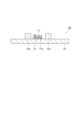
(半導体装置)
図1は、半導体装置の第一実施形態を模式的に示す断面図である。図1に示す半導体装置100は、基板10と、基板10の表面上に配置されたチップT1(第一のチップ)と、基板10の表面上であってチップT1の周囲に配置された複数の支持片Dcと、複数の支持片Dcによって支持され且つチップT1(第一のチップ)を覆うように配置された接着剤片付きチップT2cと、チップT2上に積層されたチップT3,T4と、基板10の表面上の電極(不図示)とチップT1~T4とをそれぞれ電気的に接続する複数のワイヤwと、チップT1とチップT2との隙間等に充填された封止材50とを備える。接着剤片付きチップT2cは、チップT2(第二のチップ)及びチップT2(第二のチップ)の一方の面上に設けられた接着剤片Tcを備えている。
支持片の作製方法の一例について説明する。なお、図1に示す支持片Dcは熱硬化性樹組成物が硬化した後のものである。一方、支持片Daは熱硬化性樹組成物が完全に硬化する前の状態のものである(例えば、図5(b)参照)。
半導体装置100の製造方法について説明する。本実施形態に係る製造方法は、以下の(A)~(H)の工程を含む。
(A)積層フィルム20を準備する工程(図4参照)
(B)支持片形成用フィルムDを個片化することによって、粘着層2の表面上に複数の支持片Daを形成する工程(図5(b)参照)
(C)粘着層2から支持片Daをピックアップする工程(図5(d)参照)
(D)基板10上に第一のチップT1を配置する工程
(E)基板10上であって第一のチップT1の周囲に複数の支持片Daを配置する工程(図6参照)
(F)第二のチップT2と、第二のチップT2の一方の面上に設けられた接着剤片Taとを備える接着剤片付きチップT2aを準備する工程(図7参照)
(G)複数の支持片Dcの表面上に接着剤片付きチップT2aを配置することによってドルメン構造を構築する工程(図8参照)
(H)チップT1とチップT2との隙間等を封止材50で封止する工程(図1参照)
(D)工程は、基板10上に第一のチップT1を配置する工程である。例えば、まず、基板10上の所定の位置に接着剤層T1cを介してチップT1を配置する。その後、チップT1はワイヤwで基板10と電気的に接続される。
(E)工程は、基板10上であって第一のチップT1の周囲に複数の支持片Daを配置する工程である。この工程を経て、図6に示す構造体30が作製される。構造体30は、基板10と、その表面上に配置されたチップT1と、複数の支持片Daとを備える。支持片Daの配置は圧着処理によって行えばよい。圧着処理は、例えば、80~180℃、0.01~0.50MPaの条件で、0.5~3.0秒間にわたって実施することが好ましい。なお、支持片Daは(E)工程の時点で完全に硬化して支持片Dcとなっていてもよく、この時点では完全硬化していなくてもよい。支持片Daは(G)工程の開始前の時点で完全硬化して支持片Dcとなっていることが好ましい。
(F)工程は、図7に示す接着剤片付きチップT2aを準備する工程である。接着剤片付きチップT2aは、チップT2と、その一方の表面に設けられた接着剤片Taとを備える。接着剤片付きチップT2aは、例えば、半導体ウェハ及びダイシング・ダイボンディング一体型フィルムを使用し、ダイシング工程及びピックアップ工程を経て得ることができる。
(G)工程は、複数の支持片Dcの上面に接着剤片Taが接するように、チップT1の上方に接着剤片付きチップT2aを配置する工程である。具体的には、支持片Dcの上面に接着剤片Taを介してチップT2を圧着する。この圧着処理は、例えば、80~180℃、0.01~0.50MPaの条件で、0.5~3.0秒間にわたって実施することが好ましい。次に、加熱によって接着剤片Taを硬化させる。この硬化処理は、例えば、60~175℃、0.01~1.0MPaの条件で、5分間以上にわたって実施することが好ましい。これによって、接着剤片Taが硬化して接着剤片Tcとなる。この工程を経て、基板10上にドルメン構造が構築される(図8参照)。
(H)工程は、チップT1とチップT2との隙間等を封止材50で封止する工程である。この工程を経て図1に示す半導体装置100が完成する。
支持片形成用フィルムDは、少なくとも熱硬化性樹脂層5を有する。支持片形成用フィルムDにおける熱硬化性樹脂層5を構成する熱硬化性樹脂組成物は、上述のとおり、支持片を形成したとき、支持片と接着剤片付きチップとの250℃におけるシェア強度を所定の範囲に調整し易いことから、エポキシ樹脂と、硬化剤と、エラストマとを含み、必要に応じて、無機フィラー及び硬化促進剤等を更に含むものであってよい。本発明者らの検討によると、支持片Da及び硬化後の支持片Dcは以下の特性を更に有することが好ましい。
・特性1:接着剤片付きチップT2cの接着剤片Tcとの接着強度が充分に高いこと
・特性2:基板10の所定の位置に支持片Daを熱圧着したとき位置ずれが生じ難いこと(120℃における接着剤片5pの溶融粘度(ずり粘度)が、例えば、4300~50000Pa・s又は5000~40000Pa・sであること)
・特性3:半導体装置100内において接着剤片5cが応力緩和性を発揮すること(熱硬化性樹脂組成物がエラストマ(ゴム成分)を含むこと)
・特性4:硬化に伴う収縮率が充分に小さいこと
・特性5:ピックアップ工程においてカメラによる支持片Daの視認性が良いこと(熱硬化性樹脂組成物が、例えば、着色料を含んでいること)
・特性6:接着剤片5cが充分な機械的強度を有すること
エポキシ樹脂は、硬化して接着作用を有するものであれば特に限定されない。ビスフェノールA型エポキシ樹脂、ビスフェノールF型エポキシ樹脂、ビスフェノールS型エポキシ樹脂等の二官能エポキシ樹脂、フェノールノボラック型エポキシ樹脂、クレゾールノボラック型エポキシ樹脂等のノボラック型エポキシ樹脂などを使用することができる。また、多官能エポキシ樹脂、グリシジルアミン型エポキシ樹脂、複素環含有エポキシ樹脂、脂環式エポキシ樹脂等、一般に知られているものを適用することができる。これらは一種を単独で使用してもよいし、二種以上を併用してもよい。
硬化剤としては、例えば、フェノール樹脂、エステル化合物、芳香族アミン、脂肪族アミン、酸無水物等が挙げられる。これらのうち、高いシェア強度(ダイシェア強度)を達成する観点から、フェノール樹脂が好ましい。フェノール樹脂の市販品としては、例えば、DIC株式会社製のLF-4871(商品名、BPAノボラック型フェノール樹脂)、エア・ウォーター株式会社製のHE-100C-30(商品名、フェニルアラキル型フェノール樹脂)、DIC株式会社製のフェノライトKA及びTDシリーズ、三井化学株式会社製のミレックスXLC-シリーズとXLシリーズ(例えば、ミレックスXLC-LL)、エア・ウォーター株式会社製のHEシリーズ(例えば、HE100C-30)、明和化成株式会社製のMEHC-7800シリーズ(例えば、MEHC-7800-4S)、JEFケミカル株式会社製のJDPPシリーズ、群栄化学工業株式会社製のPSMシリーズ(例えば、PSM-4326)等が挙げられる。これらは一種を単独で使用してもよいし、二種以上を併用してもよい。
エラストマとしては、例えば、アクリル樹脂、ポリエステル樹脂、ポリアミド樹脂、ポリイミド樹脂、シリコーン樹脂、ポリブタジエン、アクリロニトリル、エポキシ変性ポリブタジエン、無水マレイン酸変性ポリブタジエン、フェノール変性ポリブタジエン、カルボキシ変性アクリロニトリル等が挙げられる。
無機フィラーとしては、例えば、水酸化アルミニウム、水酸化マグネシウム、炭酸カルシウム、炭酸マグネシウム、ケイ酸カルシウム、ケイ酸マグネシウム、酸化カルシウム、酸化マグネシウム、酸化アルミニウム、窒化アルミニウム、ホウ酸アルミウィスカ、窒化ホウ素、結晶性シリカ、非晶性シリカ等が挙げられる。これらは一種を単独で使用してもよいし、二種以上を併用してもよい。
硬化促進剤としては、例えば、イミダゾール類及びその誘導体、有機リン系化合物、第二級アミン類、第三級アミン類、第四級アンモニウム塩等が挙げられる。高いシェア強度(ダイシェア強度)を達成する観点から、イミダゾール系の化合物が好ましい。イミダゾール類としては、例えば、2-メチルイミダゾール、1-ベンジル-2-メチルイミダゾール、1-シアノエチル-2-フェニルイミダゾール、1-シアノエチル-2-メチルイミダゾール等が挙げられる。これらは一種を単独で使用してもよいし、二種以上を併用してもよい。
図9は、半導体装置の第二実施形態を模式的に示す断面図である。第一実施形態に係る半導体装置100はチップT1が接着剤片Tcと離間している態様であるのに対し、本実施形態に係る半導体装置200はチップT1が接着剤片Tcと接している。つまり、接着剤片Tcは、チップT1の上面及び支持片Dcの上面に接している。例えば、支持片形成用フィルムDの厚さを適宜設定することで、チップT1の上面の位置と支持片Dcの上面の位置を一致させることができる。
・基材フィルム1と、粘着層2と、熱硬化性樹脂層5とをこの順序で備える積層フィルムを準備する工程
・上記積層フィルムの表面に熱硬化性樹脂層5よりも高い剛性を有する樹脂層6又は金属層を貼り合わせる工程
・樹脂層6又は金属層の表面に熱硬化性樹脂層5を貼り合わせる工程
<ワニスの調製>
表1に示す材料を表1に示す組成比(単位:質量部)で使用した。エポキシ樹脂、フェノール樹脂、及び無機フィラーに対して、シクロヘキサノンを加え、撹拌混合した。シクロヘキサノンの含有量は、最終的に得られるワニスにおいて、固形分割合が40質量%となるように調整した。これに、エラストマを加え、更に、カップリング剤及び硬化促進剤を加えて、各成分が均一になるまで撹拌してワニスA~Cを調製した。
・エポキシ樹脂:YDCN-700-10(商品名、新日鉄住金化学株式会社製、o-クレゾールノボラック型エポキシ樹脂、エポキシ当量:209g/eq)
・フェノール樹脂(硬化剤):HE-100C-30(商品名、エア・ウォーター株式会社製、フェノールノアラルキル型フェノール樹脂、水酸基当量:170g/eq)
・フェノール樹脂(硬化剤):PSM-4326(商品名、群栄化学工業株式会社製、フェノールノボラック型フェノール樹脂、水酸基当量:105g/eq)
・無機フィラー:アエロジルR972(商品名、日本アエロジル株式会社製、シリカ、平均粒径0.016μm)
・無機フィラー:SC2050-HLG(商品名、株式会社アドマテックス製、シリカフィラー分散液、平均粒径0.50μm)
・エラストマ:SG-P3溶剤変更品(商品名、ナガセケムテックス株式会社製、アクリルゴム、重量平均分子量:80万、Tg:12℃、溶剤:シクロヘキサノン)
・カップリング剤:A-189(商品名、GE東芝株式会社製、γ-メルカプトプロピルトリメトキシシラン)
・カップリング剤:A-1160(商品名、GE東芝株式会社製、γ-ウレイドプロピルトリエトキシシラン)
・硬化促進剤:キュアゾール2PZ-CN(商品名、四国化成工業株式会社製、1-シアノエチル-2-フェニルイミダゾール)

(製造例1)
ワニスAを100メッシュのフィルターでろ過するとともに真空脱泡した。基材フィルムとして、厚さ38μmの離型処理を施したポリエチレンテレフタレート(PET)フィルムを用意し、真空脱泡後のワニスAをPETフィルム上に塗布した。塗布したワニスAを、90℃で5分間、続いて130℃で5分間の2段階で加熱乾燥し、Bステージ状態にある製造例1の支持片形成用フィルムを得た。ワニスAの塗布量は、厚さ50μmになるよう調整した。
ワニスAをワニスBに変更した以外は、製造例1と同様にして、製造例2の支持片形成用フィルムを得た。
ワニスAをワニスCに変更した以外は、製造例1と同様にして、製造例3の支持片形成用フィルムを得た。
<接着剤片付きチップの作製>
フィルム状接着剤及び粘着フィルムを備えるダイシング・ダイボンディング一体型接着フィルム(フィルム状接着剤:厚さ50μm、粘着フィルム:厚さ110μm、日立化成株式会社製)及び厚さが400μmであるシリコンウェハを用意した。ダイシング・ダイボンディング一体型接着フィルムのフィルム状接着剤に、シリコンウェハを、ステージ温度70℃でラミネートすることによって、ダイシングサンプルを作製した。
(実施例1)
ソルダーレジスト基板(太陽ホールディングス株式会社、商品名:AUS-308)及び製造例1の支持片形成用フィルムを用意し、製造例1の支持片形成用フィルムに、ソルダーレジスト基板をステージ温度70℃でラミネートした。次いで、上記で作製した接着剤片付きチップを用意し、接着剤片付きチップの接着剤片側を、製造例1の支持片形成用フィルム上に配置し、熱圧着した。熱圧着条件は、温度120℃、時間1秒、圧力0.1MPaとした。続いて、熱圧着によって得られたサンプルを乾燥機に入れ、170℃で1時間硬化させ、実施例1の評価サンプルを作製した。
製造例1の支持片形成用フィルムを製造例2の支持片形成用フィルムに変更した以外は、実施例1と同様にして、実施例2の評価サンプルを作製した。
製造例1の支持片形成用フィルムを製造例3の支持片形成用フィルムに変更した以外は、実施例1と同様にして、実施例3の評価サンプルを作製した。
ソルダーレジスト基板(太陽ホールディングス株式会社、商品名:AUS-308)及び接着剤層付きシリコンウェハを用意し、接着剤層付きシリコンウェハの接着剤層に、ソルダーレジスト基板をステージ温度70℃でラミネートした。次いで、上記で作製した接着剤片付きチップを用意し、接着剤片付きチップの接着剤片側を、シリコンウェハ上に配置し、熱圧着した。熱圧着条件は、温度120℃、時間1秒、圧力0.1MPaとした。続いて、熱圧着によって得られたサンプルを乾燥機に入れ、170℃で1時間硬化させ、比較例1の評価サンプルを作製した。
実施例1~3及び比較例1の評価サンプルのそれぞれを用いてシェア強度を測定した。万能ボンドテスター(ノードソン・アドバンスト・テクノロジー株式会社製)を用いて、評価サンプルにおける接着剤片付きチップのチップをひっかけて引くことによって、支持片と接着剤片付きチップとの250℃におけるシェア強度を測定した。結果を表2に示す。

Claims (2)
- 基板と、前記基板上に配置された第一のチップと、前記基板上であって前記第一のチップの周囲に配置された複数の支持片と、前記複数の支持片によって支持され且つ前記第一のチップを覆うように配置された接着剤片付きチップとを含み、前記接着剤片付きチップが、第二のチップ及び前記第二のチップの一方の面上に設けられた接着剤片を含む、ドルメン構造を有する半導体装置の製造方法であって、
(A)基材フィルムと、粘着層と、少なくとも熱硬化性樹脂層を有する支持片形成用フィルムとをこの順序で備える積層フィルムを準備する工程と、
(B)前記支持片形成用フィルムを個片化することによって、前記粘着層の表面上に複数の支持片を形成する工程と、
(C)前記粘着層から前記支持片をピックアップする工程と、
(D)基板上に第一のチップを配置する工程と、
(E)前記基板上であって前記第一のチップの周囲に複数の前記支持片を配置する工程と、
(F)第二のチップと、前記第二のチップの一方の面上に設けられた、接着剤片とを備える接着剤片付きチップを準備する工程と、
(G)複数の前記支持片の表面上に前記接着剤片付きチップを配置することによってドルメン構造を構築する工程と、
を含み、
前記支持片形成用フィルムは、当該支持片形成用フィルムに接着剤片付きチップの接着剤片を熱圧着し、当該支持片形成用フィルムを170℃で1時間硬化させた後の前記支持片と前記接着剤片付きチップとの250℃におけるシェア強度が、3.2MPa以上である、半導体装置の製造方法。 - 前記支持片形成用フィルムが、熱硬化性樹脂層からなるフィルム、あるいは、熱硬化性樹脂層と、当該熱硬化性樹脂層よりも高い剛性を有する樹脂層又は金属層と、熱硬化性樹脂層とをこの順に有する三層フィルムである、請求項1に記載の半導体装置の製造方法。
Applications Claiming Priority (1)
| Application Number | Priority Date | Filing Date | Title |
|---|---|---|---|
| PCT/JP2019/017713 WO2020217404A1 (ja) | 2019-04-25 | 2019-04-25 | ドルメン構造を有する半導体装置及びその製造方法 |
Publications (3)
| Publication Number | Publication Date |
|---|---|
| JPWO2020217404A1 JPWO2020217404A1 (ja) | 2020-10-29 |
| JPWO2020217404A5 JPWO2020217404A5 (ja) | 2022-01-26 |
| JP7294410B2 true JP7294410B2 (ja) | 2023-06-20 |
Family
ID=72941128
Family Applications (1)
| Application Number | Title | Priority Date | Filing Date |
|---|---|---|---|
| JP2021515423A Active JP7294410B2 (ja) | 2019-04-25 | 2019-04-25 | ドルメン構造を有する半導体装置及びその製造方法 |
Country Status (6)
| Country | Link |
|---|---|
| US (1) | US20220157802A1 (ja) |
| JP (1) | JP7294410B2 (ja) |
| KR (1) | KR20210145737A (ja) |
| CN (1) | CN113574663A (ja) |
| SG (1) | SG11202110111YA (ja) |
| WO (1) | WO2020217404A1 (ja) |
Citations (11)
| Publication number | Priority date | Publication date | Assignee | Title |
|---|---|---|---|---|
| JP2002222889A (ja) | 2001-01-24 | 2002-08-09 | Nec Kyushu Ltd | 半導体装置及びその製造方法 |
| JP2003124433A (ja) | 2001-08-27 | 2003-04-25 | Samsung Electronics Co Ltd | マルチチップパッケージ |
| JP2006005333A (ja) | 2004-05-20 | 2006-01-05 | Toshiba Corp | 積層型電子部品とその製造方法 |
| US20070181990A1 (en) | 2006-02-03 | 2007-08-09 | Siliconware Precision Industries Co., Ltd. | Stacked semiconductor structure and fabrication method thereof |
| US20080029885A1 (en) | 2006-08-07 | 2008-02-07 | Sandisk Il Ltd. | Inverted Pyramid Multi-Die Package Reducing Wire Sweep And Weakening Torques |
| JP2013127014A (ja) | 2011-12-16 | 2013-06-27 | Hitachi Chemical Co Ltd | 接着シート |
| JP2013131557A (ja) | 2011-12-20 | 2013-07-04 | Toshiba Corp | 半導体装置およびその製造方法 |
| US20130270717A1 (en) | 2012-04-17 | 2013-10-17 | Samsung Electronics Co., Ltd. | Semiconductor package and method of fabricating the same |
| JP2015176906A (ja) | 2014-03-13 | 2015-10-05 | 株式会社東芝 | 半導体装置および半導体装置の製造方法 |
| JP2016021585A (ja) | 2012-03-08 | 2016-02-04 | 日立化成株式会社 | 接着シート及び半導体装置の製造方法 |
| JP2017515306A (ja) | 2014-04-29 | 2017-06-08 | マイクロン テクノロジー, インク. | 支持部材を有する積層半導体ダイアセンブリと、関連するシステムおよび方法 |
Family Cites Families (1)
| Publication number | Priority date | Publication date | Assignee | Title |
|---|---|---|---|---|
| US6930378B1 (en) * | 2003-11-10 | 2005-08-16 | Amkor Technology, Inc. | Stacked semiconductor die assembly having at least one support |
-
2019
- 2019-04-25 US US17/438,943 patent/US20220157802A1/en active Pending
- 2019-04-25 JP JP2021515423A patent/JP7294410B2/ja active Active
- 2019-04-25 WO PCT/JP2019/017713 patent/WO2020217404A1/ja active Application Filing
- 2019-04-25 SG SG11202110111YA patent/SG11202110111YA/en unknown
- 2019-04-25 KR KR1020217029577A patent/KR20210145737A/ko not_active Application Discontinuation
- 2019-04-25 CN CN201980094137.9A patent/CN113574663A/zh active Pending
Patent Citations (11)
| Publication number | Priority date | Publication date | Assignee | Title |
|---|---|---|---|---|
| JP2002222889A (ja) | 2001-01-24 | 2002-08-09 | Nec Kyushu Ltd | 半導体装置及びその製造方法 |
| JP2003124433A (ja) | 2001-08-27 | 2003-04-25 | Samsung Electronics Co Ltd | マルチチップパッケージ |
| JP2006005333A (ja) | 2004-05-20 | 2006-01-05 | Toshiba Corp | 積層型電子部品とその製造方法 |
| US20070181990A1 (en) | 2006-02-03 | 2007-08-09 | Siliconware Precision Industries Co., Ltd. | Stacked semiconductor structure and fabrication method thereof |
| US20080029885A1 (en) | 2006-08-07 | 2008-02-07 | Sandisk Il Ltd. | Inverted Pyramid Multi-Die Package Reducing Wire Sweep And Weakening Torques |
| JP2013127014A (ja) | 2011-12-16 | 2013-06-27 | Hitachi Chemical Co Ltd | 接着シート |
| JP2013131557A (ja) | 2011-12-20 | 2013-07-04 | Toshiba Corp | 半導体装置およびその製造方法 |
| JP2016021585A (ja) | 2012-03-08 | 2016-02-04 | 日立化成株式会社 | 接着シート及び半導体装置の製造方法 |
| US20130270717A1 (en) | 2012-04-17 | 2013-10-17 | Samsung Electronics Co., Ltd. | Semiconductor package and method of fabricating the same |
| JP2015176906A (ja) | 2014-03-13 | 2015-10-05 | 株式会社東芝 | 半導体装置および半導体装置の製造方法 |
| JP2017515306A (ja) | 2014-04-29 | 2017-06-08 | マイクロン テクノロジー, インク. | 支持部材を有する積層半導体ダイアセンブリと、関連するシステムおよび方法 |
Also Published As
| Publication number | Publication date |
|---|---|
| SG11202110111YA (en) | 2021-11-29 |
| US20220157802A1 (en) | 2022-05-19 |
| TW202044423A (zh) | 2020-12-01 |
| KR20210145737A (ko) | 2021-12-02 |
| WO2020217404A1 (ja) | 2020-10-29 |
| JPWO2020217404A1 (ja) | 2020-10-29 |
| CN113574663A (zh) | 2021-10-29 |
Similar Documents
| Publication | Publication Date | Title |
|---|---|---|
| JP7247733B2 (ja) | ドルメン構造を有する半導体装置の製造方法 | |
| WO2020100998A1 (ja) | 半導体装置及びその製造方法、並びに半導体装置の製造に使用される構造体 | |
| WO2020218526A1 (ja) | ドルメン構造を有する半導体装置及びその製造方法、並びに、支持片形成用積層フィルム及びその製造方法 | |
| JP7452545B2 (ja) | 支持片の製造方法、半導体装置の製造方法、及び支持片形成用積層フィルム | |
| WO2020218523A1 (ja) | ドルメン構造を有する半導体装置及びその製造方法、並びに、支持片形成用積層フィルム及びその製造方法 | |
| JP7294410B2 (ja) | ドルメン構造を有する半導体装置及びその製造方法 | |
| US20220149009A1 (en) | Method for manufacturing semiconductor device having dolmen structure, method for manufacturing support piece, and laminated film | |
| TWI830901B (zh) | 半導體裝置的製造方法 | |
| JP7351335B2 (ja) | ドルメン構造を有する半導体装置及びその製造方法、支持片の製造方法、並びに、支持片形成用積層フィルム | |
| WO2020217405A1 (ja) | ドルメン構造を有する半導体装置の製造方法、支持片の製造方法、及び支持片形成用積層フィルム | |
| TWI833985B (zh) | 支撐片的製造方法、半導體裝置的製造方法及支撐片形成用積層膜 | |
| WO2020218524A1 (ja) | ドルメン構造を有する半導体装置及びその製造方法、並びに、支持片形成用積層フィルム及びその製造方法 | |
| WO2020218530A1 (ja) | ドルメン構造を有する半導体装置の製造方法及び支持片の製造方法 | |
| TWI830905B (zh) | 具有支石墓結構的半導體裝置及其製造方法以及支持片形成用積層膜及其製造方法 | |
| WO2023136059A1 (ja) | 個片化体形成用積層フィルム及びその製造方法、並びに半導体装置の製造方法 | |
| WO2020218532A1 (ja) | ドルメン構造を有する半導体装置の製造方法及び支持片の製造方法 | |
| JP2022153830A (ja) | 支持部材の製造方法、及び、半導体装置の製造方法 |
Legal Events
| Date | Code | Title | Description |
|---|---|---|---|
| A521 | Request for written amendment filed |
Free format text: JAPANESE INTERMEDIATE CODE: A523 Effective date: 20210914 |
|
| A621 | Written request for application examination |
Free format text: JAPANESE INTERMEDIATE CODE: A621 Effective date: 20220204 |
|
| A131 | Notification of reasons for refusal |
Free format text: JAPANESE INTERMEDIATE CODE: A131 Effective date: 20221004 |
|
| A521 | Request for written amendment filed |
Free format text: JAPANESE INTERMEDIATE CODE: A523 Effective date: 20221202 |
|
| A131 | Notification of reasons for refusal |
Free format text: JAPANESE INTERMEDIATE CODE: A131 Effective date: 20230314 |
|
| A521 | Request for written amendment filed |
Free format text: JAPANESE INTERMEDIATE CODE: A523 Effective date: 20230419 |
|
| TRDD | Decision of grant or rejection written | ||
| A01 | Written decision to grant a patent or to grant a registration (utility model) |
Free format text: JAPANESE INTERMEDIATE CODE: A01 Effective date: 20230509 |
|
| A61 | First payment of annual fees (during grant procedure) |
Free format text: JAPANESE INTERMEDIATE CODE: A61 Effective date: 20230522 |
|
| R151 | Written notification of patent or utility model registration |
Ref document number: 7294410 Country of ref document: JP Free format text: JAPANESE INTERMEDIATE CODE: R151 |
|
| S531 | Written request for registration of change of domicile |
Free format text: JAPANESE INTERMEDIATE CODE: R313531 |
|
| R350 | Written notification of registration of transfer |
Free format text: JAPANESE INTERMEDIATE CODE: R350 |