WO2020208739A1 - 半導体装置 - Google Patents
半導体装置 Download PDFInfo
- Publication number
- WO2020208739A1 WO2020208739A1 PCT/JP2019/015603 JP2019015603W WO2020208739A1 WO 2020208739 A1 WO2020208739 A1 WO 2020208739A1 JP 2019015603 W JP2019015603 W JP 2019015603W WO 2020208739 A1 WO2020208739 A1 WO 2020208739A1
- Authority
- WO
- WIPO (PCT)
- Prior art keywords
- electrode
- semiconductor device
- main electrode
- metal frame
- metal plate
- Prior art date
- Legal status (The legal status is an assumption and is not a legal conclusion. Google has not performed a legal analysis and makes no representation as to the accuracy of the status listed.)
- Ceased
Links
Images




Classifications
-
- H—ELECTRICITY
- H10—SEMICONDUCTOR DEVICES; ELECTRIC SOLID-STATE DEVICES NOT OTHERWISE PROVIDED FOR
- H10W—GENERIC PACKAGES, INTERCONNECTIONS, CONNECTORS OR OTHER CONSTRUCTIONAL DETAILS OF DEVICES COVERED BY CLASS H10
- H10W90/00—Package configurations
-
- H—ELECTRICITY
- H10—SEMICONDUCTOR DEVICES; ELECTRIC SOLID-STATE DEVICES NOT OTHERWISE PROVIDED FOR
- H10W—GENERIC PACKAGES, INTERCONNECTIONS, CONNECTORS OR OTHER CONSTRUCTIONAL DETAILS OF DEVICES COVERED BY CLASS H10
- H10W70/00—Package substrates; Interposers; Redistribution layers [RDL]
- H10W70/40—Leadframes
- H10W70/411—Chip-supporting parts, e.g. die pads
-
- H—ELECTRICITY
- H10—SEMICONDUCTOR DEVICES; ELECTRIC SOLID-STATE DEVICES NOT OTHERWISE PROVIDED FOR
- H10W—GENERIC PACKAGES, INTERCONNECTIONS, CONNECTORS OR OTHER CONSTRUCTIONAL DETAILS OF DEVICES COVERED BY CLASS H10
- H10W70/00—Package substrates; Interposers; Redistribution layers [RDL]
- H10W70/40—Leadframes
- H10W70/421—Shapes or dispositions
- H10W70/424—Cross-sectional shapes
- H10W70/427—Bent parts
-
- H—ELECTRICITY
- H10—SEMICONDUCTOR DEVICES; ELECTRIC SOLID-STATE DEVICES NOT OTHERWISE PROVIDED FOR
- H10W—GENERIC PACKAGES, INTERCONNECTIONS, CONNECTORS OR OTHER CONSTRUCTIONAL DETAILS OF DEVICES COVERED BY CLASS H10
- H10W70/00—Package substrates; Interposers; Redistribution layers [RDL]
- H10W70/40—Leadframes
- H10W70/421—Shapes or dispositions
- H10W70/433—Shapes or dispositions of deformation-absorbing parts, e.g. leads having meandering shapes
-
- H—ELECTRICITY
- H10—SEMICONDUCTOR DEVICES; ELECTRIC SOLID-STATE DEVICES NOT OTHERWISE PROVIDED FOR
- H10W—GENERIC PACKAGES, INTERCONNECTIONS, CONNECTORS OR OTHER CONSTRUCTIONAL DETAILS OF DEVICES COVERED BY CLASS H10
- H10W70/00—Package substrates; Interposers; Redistribution layers [RDL]
- H10W70/40—Leadframes
- H10W70/464—Additional interconnections in combination with leadframes
- H10W70/468—Circuit boards
-
- H—ELECTRICITY
- H10—SEMICONDUCTOR DEVICES; ELECTRIC SOLID-STATE DEVICES NOT OTHERWISE PROVIDED FOR
- H10W—GENERIC PACKAGES, INTERCONNECTIONS, CONNECTORS OR OTHER CONSTRUCTIONAL DETAILS OF DEVICES COVERED BY CLASS H10
- H10W70/00—Package substrates; Interposers; Redistribution layers [RDL]
- H10W70/60—Insulating or insulated package substrates; Interposers; Redistribution layers
- H10W70/611—Insulating or insulated package substrates; Interposers; Redistribution layers for connecting multiple chips together
-
- H—ELECTRICITY
- H10—SEMICONDUCTOR DEVICES; ELECTRIC SOLID-STATE DEVICES NOT OTHERWISE PROVIDED FOR
- H10W—GENERIC PACKAGES, INTERCONNECTIONS, CONNECTORS OR OTHER CONSTRUCTIONAL DETAILS OF DEVICES COVERED BY CLASS H10
- H10W70/00—Package substrates; Interposers; Redistribution layers [RDL]
- H10W70/60—Insulating or insulated package substrates; Interposers; Redistribution layers
- H10W70/62—Insulating or insulated package substrates; Interposers; Redistribution layers characterised by their interconnections
- H10W70/65—Shapes or dispositions of interconnections
-
- H—ELECTRICITY
- H10—SEMICONDUCTOR DEVICES; ELECTRIC SOLID-STATE DEVICES NOT OTHERWISE PROVIDED FOR
- H10W—GENERIC PACKAGES, INTERCONNECTIONS, CONNECTORS OR OTHER CONSTRUCTIONAL DETAILS OF DEVICES COVERED BY CLASS H10
- H10W70/00—Package substrates; Interposers; Redistribution layers [RDL]
- H10W70/60—Insulating or insulated package substrates; Interposers; Redistribution layers
- H10W70/62—Insulating or insulated package substrates; Interposers; Redistribution layers characterised by their interconnections
- H10W70/65—Shapes or dispositions of interconnections
- H10W70/658—Shapes or dispositions of interconnections for devices provided for in groups H10D8/00 - H10D48/00
-
- H—ELECTRICITY
- H10—SEMICONDUCTOR DEVICES; ELECTRIC SOLID-STATE DEVICES NOT OTHERWISE PROVIDED FOR
- H10W—GENERIC PACKAGES, INTERCONNECTIONS, CONNECTORS OR OTHER CONSTRUCTIONAL DETAILS OF DEVICES COVERED BY CLASS H10
- H10W90/00—Package configurations
- H10W90/701—Package configurations characterised by the relative positions of pads or connectors relative to package parts
-
- H—ELECTRICITY
- H10—SEMICONDUCTOR DEVICES; ELECTRIC SOLID-STATE DEVICES NOT OTHERWISE PROVIDED FOR
- H10W—GENERIC PACKAGES, INTERCONNECTIONS, CONNECTORS OR OTHER CONSTRUCTIONAL DETAILS OF DEVICES COVERED BY CLASS H10
- H10W40/00—Arrangements for thermal protection or thermal control
- H10W40/20—Arrangements for cooling
- H10W40/25—Arrangements for cooling characterised by their materials
- H10W40/255—Arrangements for cooling characterised by their materials having a laminate or multilayered structure, e.g. direct bond copper [DBC] ceramic substrates
-
- H—ELECTRICITY
- H10—SEMICONDUCTOR DEVICES; ELECTRIC SOLID-STATE DEVICES NOT OTHERWISE PROVIDED FOR
- H10W—GENERIC PACKAGES, INTERCONNECTIONS, CONNECTORS OR OTHER CONSTRUCTIONAL DETAILS OF DEVICES COVERED BY CLASS H10
- H10W40/00—Arrangements for thermal protection or thermal control
- H10W40/70—Fillings or auxiliary members in containers or in encapsulations for thermal protection or control
- H10W40/77—Auxiliary members characterised by their shape
- H10W40/778—Auxiliary members characterised by their shape in encapsulations
-
- H—ELECTRICITY
- H10—SEMICONDUCTOR DEVICES; ELECTRIC SOLID-STATE DEVICES NOT OTHERWISE PROVIDED FOR
- H10W—GENERIC PACKAGES, INTERCONNECTIONS, CONNECTORS OR OTHER CONSTRUCTIONAL DETAILS OF DEVICES COVERED BY CLASS H10
- H10W70/00—Package substrates; Interposers; Redistribution layers [RDL]
- H10W70/40—Leadframes
- H10W70/464—Additional interconnections in combination with leadframes
-
- H—ELECTRICITY
- H10—SEMICONDUCTOR DEVICES; ELECTRIC SOLID-STATE DEVICES NOT OTHERWISE PROVIDED FOR
- H10W—GENERIC PACKAGES, INTERCONNECTIONS, CONNECTORS OR OTHER CONSTRUCTIONAL DETAILS OF DEVICES COVERED BY CLASS H10
- H10W70/00—Package substrates; Interposers; Redistribution layers [RDL]
- H10W70/40—Leadframes
- H10W70/464—Additional interconnections in combination with leadframes
- H10W70/466—Tape carriers or flat leads
-
- H—ELECTRICITY
- H10—SEMICONDUCTOR DEVICES; ELECTRIC SOLID-STATE DEVICES NOT OTHERWISE PROVIDED FOR
- H10W—GENERIC PACKAGES, INTERCONNECTIONS, CONNECTORS OR OTHER CONSTRUCTIONAL DETAILS OF DEVICES COVERED BY CLASS H10
- H10W72/00—Interconnections or connectors in packages
- H10W72/071—Connecting or disconnecting
- H10W72/073—Connecting or disconnecting of die-attach connectors
- H10W72/07351—Connecting or disconnecting of die-attach connectors characterised by changes in properties of the die-attach connectors during connecting
- H10W72/07354—Connecting or disconnecting of die-attach connectors characterised by changes in properties of the die-attach connectors during connecting changes in dispositions
-
- H—ELECTRICITY
- H10—SEMICONDUCTOR DEVICES; ELECTRIC SOLID-STATE DEVICES NOT OTHERWISE PROVIDED FOR
- H10W—GENERIC PACKAGES, INTERCONNECTIONS, CONNECTORS OR OTHER CONSTRUCTIONAL DETAILS OF DEVICES COVERED BY CLASS H10
- H10W72/00—Interconnections or connectors in packages
- H10W72/071—Connecting or disconnecting
- H10W72/076—Connecting or disconnecting of strap connectors
-
- H—ELECTRICITY
- H10—SEMICONDUCTOR DEVICES; ELECTRIC SOLID-STATE DEVICES NOT OTHERWISE PROVIDED FOR
- H10W—GENERIC PACKAGES, INTERCONNECTIONS, CONNECTORS OR OTHER CONSTRUCTIONAL DETAILS OF DEVICES COVERED BY CLASS H10
- H10W72/00—Interconnections or connectors in packages
- H10W72/071—Connecting or disconnecting
- H10W72/076—Connecting or disconnecting of strap connectors
- H10W72/07621—Aligning
- H10W72/07627—Aligning involving guiding structures, e.g. spacers or supporting members
-
- H—ELECTRICITY
- H10—SEMICONDUCTOR DEVICES; ELECTRIC SOLID-STATE DEVICES NOT OTHERWISE PROVIDED FOR
- H10W—GENERIC PACKAGES, INTERCONNECTIONS, CONNECTORS OR OTHER CONSTRUCTIONAL DETAILS OF DEVICES COVERED BY CLASS H10
- H10W72/00—Interconnections or connectors in packages
- H10W72/071—Connecting or disconnecting
- H10W72/076—Connecting or disconnecting of strap connectors
- H10W72/07631—Techniques
- H10W72/07636—Soldering or alloying
-
- H—ELECTRICITY
- H10—SEMICONDUCTOR DEVICES; ELECTRIC SOLID-STATE DEVICES NOT OTHERWISE PROVIDED FOR
- H10W—GENERIC PACKAGES, INTERCONNECTIONS, CONNECTORS OR OTHER CONSTRUCTIONAL DETAILS OF DEVICES COVERED BY CLASS H10
- H10W72/00—Interconnections or connectors in packages
- H10W72/071—Connecting or disconnecting
- H10W72/076—Connecting or disconnecting of strap connectors
- H10W72/07651—Connecting or disconnecting of strap connectors characterised by changes in properties of the strap connectors during connecting
- H10W72/07652—Connecting or disconnecting of strap connectors characterised by changes in properties of the strap connectors during connecting changes in structures or sizes
-
- H—ELECTRICITY
- H10—SEMICONDUCTOR DEVICES; ELECTRIC SOLID-STATE DEVICES NOT OTHERWISE PROVIDED FOR
- H10W—GENERIC PACKAGES, INTERCONNECTIONS, CONNECTORS OR OTHER CONSTRUCTIONAL DETAILS OF DEVICES COVERED BY CLASS H10
- H10W72/00—Interconnections or connectors in packages
- H10W72/30—Die-attach connectors
- H10W72/341—Dispositions of die-attach connectors, e.g. layouts
- H10W72/347—Dispositions of multiple die-attach connectors
-
- H—ELECTRICITY
- H10—SEMICONDUCTOR DEVICES; ELECTRIC SOLID-STATE DEVICES NOT OTHERWISE PROVIDED FOR
- H10W—GENERIC PACKAGES, INTERCONNECTIONS, CONNECTORS OR OTHER CONSTRUCTIONAL DETAILS OF DEVICES COVERED BY CLASS H10
- H10W72/00—Interconnections or connectors in packages
- H10W72/30—Die-attach connectors
- H10W72/351—Materials of die-attach connectors
- H10W72/352—Materials of die-attach connectors comprising metals or metalloids, e.g. solders
-
- H—ELECTRICITY
- H10—SEMICONDUCTOR DEVICES; ELECTRIC SOLID-STATE DEVICES NOT OTHERWISE PROVIDED FOR
- H10W—GENERIC PACKAGES, INTERCONNECTIONS, CONNECTORS OR OTHER CONSTRUCTIONAL DETAILS OF DEVICES COVERED BY CLASS H10
- H10W72/00—Interconnections or connectors in packages
- H10W72/30—Die-attach connectors
- H10W72/381—Auxiliary members
-
- H—ELECTRICITY
- H10—SEMICONDUCTOR DEVICES; ELECTRIC SOLID-STATE DEVICES NOT OTHERWISE PROVIDED FOR
- H10W—GENERIC PACKAGES, INTERCONNECTIONS, CONNECTORS OR OTHER CONSTRUCTIONAL DETAILS OF DEVICES COVERED BY CLASS H10
- H10W72/00—Interconnections or connectors in packages
- H10W72/60—Strap connectors, e.g. thick copper clips for grounding of power devices
- H10W72/621—Structures or relative sizes of strap connectors
- H10W72/627—Multiple strap connectors having different structures or shapes
-
- H—ELECTRICITY
- H10—SEMICONDUCTOR DEVICES; ELECTRIC SOLID-STATE DEVICES NOT OTHERWISE PROVIDED FOR
- H10W—GENERIC PACKAGES, INTERCONNECTIONS, CONNECTORS OR OTHER CONSTRUCTIONAL DETAILS OF DEVICES COVERED BY CLASS H10
- H10W72/00—Interconnections or connectors in packages
- H10W72/60—Strap connectors, e.g. thick copper clips for grounding of power devices
- H10W72/631—Shapes of strap connectors
-
- H—ELECTRICITY
- H10—SEMICONDUCTOR DEVICES; ELECTRIC SOLID-STATE DEVICES NOT OTHERWISE PROVIDED FOR
- H10W—GENERIC PACKAGES, INTERCONNECTIONS, CONNECTORS OR OTHER CONSTRUCTIONAL DETAILS OF DEVICES COVERED BY CLASS H10
- H10W72/00—Interconnections or connectors in packages
- H10W72/60—Strap connectors, e.g. thick copper clips for grounding of power devices
- H10W72/641—Dispositions of strap connectors
- H10W72/646—Dispositions of strap connectors the connected ends being on auxiliary connecting means on bond pads, e.g. on a bump connector
-
- H—ELECTRICITY
- H10—SEMICONDUCTOR DEVICES; ELECTRIC SOLID-STATE DEVICES NOT OTHERWISE PROVIDED FOR
- H10W—GENERIC PACKAGES, INTERCONNECTIONS, CONNECTORS OR OTHER CONSTRUCTIONAL DETAILS OF DEVICES COVERED BY CLASS H10
- H10W72/00—Interconnections or connectors in packages
- H10W72/60—Strap connectors, e.g. thick copper clips for grounding of power devices
- H10W72/651—Materials of strap connectors
- H10W72/652—Materials of strap connectors comprising metals or metalloids, e.g. silver
-
- H—ELECTRICITY
- H10—SEMICONDUCTOR DEVICES; ELECTRIC SOLID-STATE DEVICES NOT OTHERWISE PROVIDED FOR
- H10W—GENERIC PACKAGES, INTERCONNECTIONS, CONNECTORS OR OTHER CONSTRUCTIONAL DETAILS OF DEVICES COVERED BY CLASS H10
- H10W72/00—Interconnections or connectors in packages
- H10W72/851—Dispositions of multiple connectors or interconnections
- H10W72/853—On the same surface
- H10W72/871—Bond wires and strap connectors
-
- H—ELECTRICITY
- H10—SEMICONDUCTOR DEVICES; ELECTRIC SOLID-STATE DEVICES NOT OTHERWISE PROVIDED FOR
- H10W—GENERIC PACKAGES, INTERCONNECTIONS, CONNECTORS OR OTHER CONSTRUCTIONAL DETAILS OF DEVICES COVERED BY CLASS H10
- H10W72/00—Interconnections or connectors in packages
- H10W72/851—Dispositions of multiple connectors or interconnections
- H10W72/874—On different surfaces
- H10W72/884—Die-attach connectors and bond wires
-
- H—ELECTRICITY
- H10—SEMICONDUCTOR DEVICES; ELECTRIC SOLID-STATE DEVICES NOT OTHERWISE PROVIDED FOR
- H10W—GENERIC PACKAGES, INTERCONNECTIONS, CONNECTORS OR OTHER CONSTRUCTIONAL DETAILS OF DEVICES COVERED BY CLASS H10
- H10W72/00—Interconnections or connectors in packages
- H10W72/90—Bond pads, in general
- H10W72/921—Structures or relative sizes of bond pads
- H10W72/926—Multiple bond pads having different sizes
-
- H—ELECTRICITY
- H10—SEMICONDUCTOR DEVICES; ELECTRIC SOLID-STATE DEVICES NOT OTHERWISE PROVIDED FOR
- H10W—GENERIC PACKAGES, INTERCONNECTIONS, CONNECTORS OR OTHER CONSTRUCTIONAL DETAILS OF DEVICES COVERED BY CLASS H10
- H10W72/00—Interconnections or connectors in packages
- H10W72/90—Bond pads, in general
- H10W72/941—Dispositions of bond pads
- H10W72/944—Dispositions of multiple bond pads
-
- H—ELECTRICITY
- H10—SEMICONDUCTOR DEVICES; ELECTRIC SOLID-STATE DEVICES NOT OTHERWISE PROVIDED FOR
- H10W—GENERIC PACKAGES, INTERCONNECTIONS, CONNECTORS OR OTHER CONSTRUCTIONAL DETAILS OF DEVICES COVERED BY CLASS H10
- H10W74/00—Encapsulations, e.g. protective coatings
-
- H—ELECTRICITY
- H10—SEMICONDUCTOR DEVICES; ELECTRIC SOLID-STATE DEVICES NOT OTHERWISE PROVIDED FOR
- H10W—GENERIC PACKAGES, INTERCONNECTIONS, CONNECTORS OR OTHER CONSTRUCTIONAL DETAILS OF DEVICES COVERED BY CLASS H10
- H10W90/00—Package configurations
- H10W90/701—Package configurations characterised by the relative positions of pads or connectors relative to package parts
- H10W90/731—Package configurations characterised by the relative positions of pads or connectors relative to package parts of die-attach connectors
- H10W90/734—Package configurations characterised by the relative positions of pads or connectors relative to package parts of die-attach connectors between a chip and a stacked insulating package substrate, interposer or RDL
-
- H—ELECTRICITY
- H10—SEMICONDUCTOR DEVICES; ELECTRIC SOLID-STATE DEVICES NOT OTHERWISE PROVIDED FOR
- H10W—GENERIC PACKAGES, INTERCONNECTIONS, CONNECTORS OR OTHER CONSTRUCTIONAL DETAILS OF DEVICES COVERED BY CLASS H10
- H10W90/00—Package configurations
- H10W90/701—Package configurations characterised by the relative positions of pads or connectors relative to package parts
- H10W90/731—Package configurations characterised by the relative positions of pads or connectors relative to package parts of die-attach connectors
- H10W90/736—Package configurations characterised by the relative positions of pads or connectors relative to package parts of die-attach connectors between a chip and a stacked lead frame, conducting package substrate or heat sink
-
- H—ELECTRICITY
- H10—SEMICONDUCTOR DEVICES; ELECTRIC SOLID-STATE DEVICES NOT OTHERWISE PROVIDED FOR
- H10W—GENERIC PACKAGES, INTERCONNECTIONS, CONNECTORS OR OTHER CONSTRUCTIONAL DETAILS OF DEVICES COVERED BY CLASS H10
- H10W90/00—Package configurations
- H10W90/701—Package configurations characterised by the relative positions of pads or connectors relative to package parts
- H10W90/751—Package configurations characterised by the relative positions of pads or connectors relative to package parts of bond wires
- H10W90/754—Package configurations characterised by the relative positions of pads or connectors relative to package parts of bond wires between a chip and a stacked insulating package substrate, interposer or RDL
-
- H—ELECTRICITY
- H10—SEMICONDUCTOR DEVICES; ELECTRIC SOLID-STATE DEVICES NOT OTHERWISE PROVIDED FOR
- H10W—GENERIC PACKAGES, INTERCONNECTIONS, CONNECTORS OR OTHER CONSTRUCTIONAL DETAILS OF DEVICES COVERED BY CLASS H10
- H10W90/00—Package configurations
- H10W90/701—Package configurations characterised by the relative positions of pads or connectors relative to package parts
- H10W90/761—Package configurations characterised by the relative positions of pads or connectors relative to package parts of strap connectors
- H10W90/764—Package configurations characterised by the relative positions of pads or connectors relative to package parts of strap connectors between a chip and a stacked insulating package substrate, interposer or RDL
Definitions
- the present invention relates to a semiconductor device.
- a thick metal frame is used for reasons such as passing a large current.
- a thick metal frame has high rigidity, and it is necessary to secure the thickness of the conductive joint material at the joint in order to relax the rigidity.
- a semiconductor device for ensuring the thickness of the conductive bonding material between the semiconductor element and the metal frame
- a semiconductor device for ensuring the thickness of the conductive bonding material between the semiconductor element and the metal frame
- a convex portion 941 is provided on a terminal 911 (913) facing the semiconductor element 995 (of a metal frame), and a conductive bonding material is provided between the semiconductor element 995 and the terminal 911 (913).
- (Conductive adhesive, solder, etc.) 975 is arranged.
- Reference numeral 999 is a jig.
- the above-mentioned semiconductor device is excellent in that the thickness of the conductive bonding material 975 can be secured if the electrodes of the bonding portion of the semiconductor element are the same main electrode.
- An object of the present invention is to provide a semiconductor device capable of forming a thick layer of a conductive bonding material between a main electrode and a metal frame.
- the semiconductor device of the present invention includes a circuit board, a semiconductor element mounted on the circuit board and having a main electrode on a surface opposite to the side facing the circuit board, and the main electrode side of the semiconductor element.
- a semiconductor device comprising a metal frame arranged in the above, and a conductive bonding material is arranged between the main electrode and the metal frame to electrically connect the main electrode and the metal frame.
- the main electrode and the sub-electrode are formed on the metal frame side of the element, and the semiconductor device is a metal having a convex portion formed at a position corresponding to the main electrode between the metal frame and the main electrode.
- the feature is that the boards are arranged.
- the "circuit board” is originally an insulator board mainly composed of ceramics, glass epoxy resin, etc., has no semiconductor element attached, and has wiring such as copper foil and aluminum foil. It is a general term for a wiring board and a circuit board on which electronic components such as semiconductor elements are mounted.
- the "semiconductor element” refers to a circuit element made of a semiconductor. As the material of the semiconductor device, there are those using single crystal silicon, those using germanium, gallium arsenide (GaAs), gallium arsenide phosphorus, gallium nitride (GaN), silicon carbide (SiC) and the like.
- semiconductor element examples include MOS (abbreviation of ether-Oxide Semiconductor, semiconductor of metal-oxide-semiconductor structure, MOSFET, CMOS, etc.), IGBT (abbreviation of Integrated-Gate-Bipolar-Transistor, insulated gate type bipolar). There are transistors), diodes, thyristors, etc.
- MOS abbreviation of ether-Oxide Semiconductor, semiconductor of metal-oxide-semiconductor structure, MOSFET, CMOS, etc.
- IGBT abbreviation of Integrated-Gate-Bipolar-Transistor, insulated gate type bipolar
- MOS abbreviation of MOS, MOSFET, CMOS, etc.
- the main electrode is an electrode that is compared with a sub-electrode, and the magnitude of the current flowing through the electrode (main electrode) is equal to or greater than the magnitude of the current flowing through the sub-electrode.
- the source electrode and the drain electrode are main electrodes
- the gate electrode is a sub electrode.
- a so-called power semiconductor element that handles power with a so-called metal electrode a high voltage is applied between the source electrode and the drain electrode, a large current flows through the source electrode and the drain electrode (main electrode), and a gate electrode (secondary electrode).
- Is used for controlling the switching operation between the source electrode and the drain electrode, and the current flowing through the gate electrode is smaller than that of the source electrode and the drain electrode.
- the number of main electrodes is not limited to one.
- the A electrode and the B electrode can be used as the main electrode
- the C electrode can be used as the sub electrode.
- the semiconductor element contains two diodes (both anode electrodes are connected to external terminals, both cathode electrodes are connected to each other and connected to the external terminals, and the anode electrodes face the metal frame.
- the magnitudes of the currents flowing through the two diodes are almost the same, one of the anode electrodes can be used as the main electrode and the other can be used as the sub-electrode. "Almost the same” means a case where the magnitude of one current is 100 and the magnitude of the other current is 80 to 120.
- the metal frame is made of a metal such as copper or iron, and constitutes the framework of the semiconductor device. Examples of metal frames include lead frames, clips and the like. The metal frame is electrically connected to the main electrode.
- the conductive bonding material refers to a bonding material having conductivity typified by solder. Usually, by melting by reflow or the like, electrical bonding between the main electrode and the metal frame is performed.
- a metal plate is a plate made of a metal such as copper or iron.
- the metal plate is preferably the same type as the metal frame. For example, when the metal frame is copper, the metal plate is also copper, and when the metal frame is iron, the metal plate is preferably of the same type as iron. This is because the coefficients of thermal expansion of the metal frame and the metal plate are the same or close to each other.
- the convex part means a protruding part, a raised part, or a bulging part. It is a part that protrudes from the surface of the metal plate.
- a convex portion can be easily formed.
- a concave portion is formed on the surface opposite to the surface on which the convex portion is formed.
- a metal plate having a convex portion formed at a position corresponding to the main electrode is arranged between the metal frame and the main electrode means "the main electrode is located between the metal frame and the sub-electrode.” It is not intended to exclude that a metal plate having a convex portion formed at a position corresponding to is arranged (arranged).
- a layer of the conductive bonding material is formed between the metal plate and the metal frame.
- the layer of the conductive joining member referred to here means a layer of the conductive joining member formed between the metal plate and the metal frame so that the metal plate and the metal frame do not come into contact with each other.
- the metal plate is formed with a plurality of the convex portions.
- the main electrode has a plurality of regions, and the metal plate is formed with the convex portion for each of the plurality of regions of the main electrode. ..
- the main electrode has a plurality of regions
- the source electrode main electrode
- the source electrode main electrode is not composed of a mass region such as a square or a rectangle, but is a set of a plurality of rectangular regions. It refers to a certain case.
- the plurality of regions are independently formed.
- a wiring member is further provided on the sub-electrode side of the semiconductor element, and the metal plate is not arranged between the metal frame and the sub-electrode.
- the wiring member is a member that is joined to the sub-electrode via a conductive joining material or directly, and has conductivity.
- Examples of the wiring member include a metal piece, a metal wire, and the like.
- the convex portion of the metal plate is formed on the surface of the metal plate on the main electrode side.
- the convex portions of the metal plate are formed on both surfaces of the metal plate.
- the thickness of the metal plate is preferably equal to or less than the thickness of the metal frame.
- the semiconductor element has a source electrode as a main electrode and a gate electrode as a sub-electrode formed on the surface of the semiconductor element on the metal frame side, and is formed on the circuit board side. It is preferable that the drain electrode is formed.
- the semiconductor element has a source electrode and a drain electrode as the main electrode and a gate electrode as the sub-electrode formed on the surface of the semiconductor element on the metal frame side. Is preferable.
- a plurality of the semiconductor elements are mounted on the circuit board, and the metal plate is arranged between the main electrode and the metal frame of each of the semiconductor elements. preferable.
- the semiconductor device of the present invention since a metal plate having a convex portion formed at a position corresponding to the main electrode is arranged between the metal frame and the main electrode, it is easy to form a fine convex portion thinner than the metal frame. Since the metal plate has a structure in which the conductive bonding material gathers and joins around the convex portion of the metal plate, a short circuit between the main electrode and the sub electrode may occur even if the metal frame is thick. On the other hand, it is possible to provide a semiconductor device capable of forming a thick layer of a conductive bonding material between a main electrode and a metal frame.
- the metal frame and the main electrode are joined by a conductive bonding material via a metal plate having a convex portion formed at a position corresponding to the main electrode, but by a fine convex portion (a metal thinner than the metal frame).
- the plate is easier to form fine protrusions than the metal frame), and the conductive bonding material has a structure in which it gathers and joins at the position corresponding to the main electrode, so even if the metal frame is thick, the main electrode and the sub-electrode can be connected. It is possible to provide a semiconductor device capable of thickening the layer of the conductive bonding material while the possibility of short circuit between them is low.
- FIG. 7 (A) and 7 (B) are diagrams for explaining the semiconductor device 100-2 according to the second embodiment.
- FIG. 7 (A) and 7 (B) are diagrams for explaining the semiconductor device 100-2 according to the second embodiment.
- FIG. 8A is a diagram for explaining the semiconductor device 100-3 according to the third embodiment.
- FIG. 8B is a diagram for explaining the semiconductor device 100-4 according to the fourth embodiment.
- FIG. 8C is a diagram for explaining the semiconductor device 100-5 according to the fifth embodiment.
- FIG. 9A is a diagram for explaining the semiconductor device 100-6 according to the sixth embodiment.
- FIG. 9B is a diagram for explaining the semiconductor device 100-7 according to the seventh embodiment.
- FIG. 10A is a diagram for explaining the semiconductor device 100-8 according to the eighth embodiment.
- FIG. 10B is a diagram for explaining the semiconductor device 100-9 according to the ninth embodiment.
- FIG. 11 is a diagram for explaining the semiconductor device 100-10 according to the tenth embodiment.
- FIG. 12 (A) and 12 (B) are diagrams for explaining the semiconductor device 100-11 according to the eleventh embodiment.
- FIG. 12A is a diagram for explaining the circuit of the semiconductor device 100-11
- FIG. 12B is a diagram for explaining the internal structure of the semiconductor device 100-11. It is a figure for demonstrating the conventional semiconductor device.
- FIG. 1 is a schematic cross-sectional view of the semiconductor device 100 according to the first embodiment (a partial cross-sectional view taken along the arrow A of FIG. 4 described later).
- FIG. 2 is a diagram for explaining a circuit of the semiconductor device 100 according to the first embodiment.
- FIG. 3 is a diagram for explaining the appearance of the semiconductor device 100 according to the first embodiment.
- FIG. 4 is a diagram for explaining the internal structure of the semiconductor device 100 according to the first embodiment (a diagram showing the mold resin 6 omitted).
- the semiconductor device 100 includes a circuit board 2 and a semiconductor element 1 mounted on the circuit board 2 and having a main electrode (source electrode) 11 on a surface opposite to the side facing the circuit board 2.
- a metal frame 31 arranged on the main electrode (source electrode) 11 side is provided.
- a conductive bonding material 51 is arranged between the main electrode (source electrode) 11 and the metal frame 31 to electrically connect the main electrode 11 and the metal frame 31.
- Reference numeral 14 is a substrate of the semiconductor element 1, which is composed of silicon, germanium, gallium arsenide, or the like.
- a main electrode (source electrode) 11 and a sub-electrode 12 are formed on the metal frame 31 side of the semiconductor element 1.
- the semiconductor element 1 used in the semiconductor device 100 of FIG. 1 is a so-called power semiconductor element used for power or the like, and the semiconductor device 100 is a power semiconductor device for power control or the like.
- Semiconductor devices are also referred to as semiconductor modules.
- a heat radiating member 7 is provided on the surface of the circuit board 2 opposite to the surface on which the semiconductor element 1 is mounted.
- the heat radiating member 7 is formed of a plate-shaped metal layer such as copper, iron, or aluminum. In principle, it is insulated from the circuit of the semiconductor element 1, but it may be connected to the ground electrode of the device that uses the semiconductor device 100.
- the semiconductor element 1 has an electrode (drain electrode) 13 formed on the surface on the circuit board 2 side.
- the electrode (drain electrode) 13 is connected to the pattern wiring layer 21 on the circuit board 2 via a solder (conductive bonding material) 53, and is connected to the terminal 9D1 (see FIGS. 2 to 4).
- a main electrode (source electrode) 11 and a sub-electrode 12 are formed on the surface of the semiconductor element 1 opposite to the side facing the circuit board 2, that is, the upper surface of FIG.
- the metal plate 4 is arranged between the metal frame 31 and the main electrode (source electrode) 11, but the position corresponding to the main electrode (source electrode) 11 (semiconductor device 100 is viewed from the direction perpendicular to the circuit board 2).
- the metal plate 4 and the main electrode (source electrode) 11 overlap each other).
- a convex portion 41 is formed at a position corresponding to the main electrode (source electrode) 11 of the metal plate 4.
- solder (conductive bonding material) 51 gathers and joins around the convex portion 41 of the metal plate 4, so that the main electrode existing on the metal frame 31 side of the semiconductor element 1 is formed. While it is possible to prevent a short circuit between the (source electrode) 11 and the sub-electrode 12, a thick layer of solder (conductive bonding material) 51 and 52 is formed between the main electrode (source electrode) 11 and the metal frame 31. Is possible.
- a plurality of convex portions 41 are formed on the metal plate 4.
- more solder (conductive bonding material) 51 gathers around the convex portions 41, so that a short circuit between the main electrode (source electrode) 11 and the sub electrode 12 is caused. It can be further prevented.
- the metal plate 4 When the metal plate 4 is placed on the semiconductor element 1 with the convex portion 41 facing down, the metal plate 4 can be stably placed on the semiconductor element 1 if three or more convex portions 41 are formed. ..
- the main electrode (source electrode) 11 has four regions, and the metal plate 4 has a convex portion 41 for each of the four regions of the main electrode (source electrode) 11. It is formed (see FIG. 8).
- the solder (conductive bonding material) 51 gathers around the respective convex portions 41 formed corresponding to the four regions of the main electrode (source electrode) 11, so that a plurality of solders (conductive bonding materials) 51 are collected. 51 layers of solder (conductive bonding material) can be formed in this region with high positional accuracy, and a short circuit between the main electrode (source electrode) 11 and the sub-electrode 12 can be further prevented. If the four regions of the main electrode (source electrode) 11 are provided independently, the solder (conductive bonding material) 51 tends to gather around the respective convex portions 41.
- the metal plate 4 and the main electrode (source electrode) 11 or the convex portion 41 and the main electrode (source) are formed. It is easy to accurately take the relative position with the electrode) 11.
- the sub-electrode (gate electrode) 12 is electrically connected to the terminals 9G1 and 9G2 via a wiring member 32 such as solder (). (See FIGS. 2 and 7).
- a wiring member 32 such as solder ().
- solder solder
- As the wiring member 32 a metal piece similar to the metal frame 31 was used. The thickness of the metal pieces constituting the wiring member was made thinner than that of the metal frame 31 (the cross-sectional area was made smaller). What is the current flowing through the auxiliary electrode (gate electrode) 12? This is because it is smaller than the current flowing between the main electrode (source electrode) 11 and the electrode (drain electrode) 13.
- the entire semiconductor device 100 is covered with an insulating mold resin 6.
- the heat radiating member 7 is exposed in order to improve the heat radiating effect.
- the terminals (terminals 9G1, 9G2, 9S1D1, 9D2, 9S2, see FIGS. 2 to 4 and 7) are also exposed due to the electrical connection between the circuit of the semiconductor element 1 and the external circuit of the semiconductor device 100. There is.
- terminals 9G1, 9G2, 9S1D1, 9D2, 9S2 may be so-called pin terminals.
- the pin terminal is a metal terminal used for electrically connecting the semiconductor device 100 by inserting it into or soldering to the connector, circuit board, or connector of the other party to which the semiconductor device 100 is used.
- copper-based materials such as brass and phosphor bronze are used, they are excellent in strength and electrical conductivity, and when tin plating, gold plating, etc. are applied, they are excellent in corrosion resistance and solder wettability.
- terminals 9G1, 9G2, 9S1D1, 9D2, 9S2 are extended to the end where the circuit board 2 is extended as shown in FIGS. 3 and 4, and are bent in the direction perpendicular to the circuit board 2 (semiconductor device 100).
- the semiconductor element 1 may be bent in the direction perpendicular to the circuit board 2 from a position close to the semiconductor element 1 and may be projected from the upper surface of the semiconductor device 100 shown in FIG. By doing so, the distance between each electrode and the terminal of the semiconductor element 1 (1A, 1B) becomes shorter, and it is possible to further reduce the power loss due to the inductance.
- the convex portion 41 of the metal plate 4 is formed on the opposite surface of the main electrode (source electrode) 11 of the metal plate 4.
- the layers of the solder (conductive bonding material) 51 and 52 between the main electrode (source electrode) 11 and the convex portion 41 can be thickened, and the main electrode (source electrode) 11 can be easily protected from thermal stress. ..
- the convex portions 41 of the metal plate 4 may be formed on both surfaces of the metal plate 4. In this way, the distance between the metal plate 4 and the main electrode (source electrode) 11 and the distance between the metal plate 4 and the metal frame 31 can be at least the convex portion 41 or more.
- the thickness of the metal frame 31 is t2, the protrusion of the convex portion 41 is t11, the distance between both sides of the metal plate 4 including the protrusion of the convex portion 41 is t12, and the distance between the semiconductor element 1 and the metal frame 31 is t3.
- the thickness t1 of the metal plate 4 is equal to or less than the thickness t2 of the metal frame 31.
- the sub-electrode 12 is joined to the wiring member 32 by a solder (conductive bonding material) 54 (see FIG. 1), but the current flowing through the sub-electrode 12 is between the main electrode (source electrode) 11 and the electrode (drain electrode) 13.
- the thickness (cross-sectional area) of the wiring member 32 is smaller than that of the metal frame 31 because it is smaller than the current flowing through the wiring member 32.
- a main electrode (source electrode) 11 and a sub-electrode 12 are formed on the surface of the semiconductor element 1 on the metal frame 31 side, and an electrode (drain electrode) 13 is formed on the circuit board 2 side. ..
- the semiconductor element 1 having such a structure has been highly evaluated as a low-loss semiconductor element, and the semiconductor device 100 equipped with the semiconductor element 1 is suitable for power or the like.
- the semiconductor element 1 may have a main electrode (source electrode) 11, an electrode (drain electrode) 13, and a sub-electrode 12 formed on the surface of the semiconductor element 1 on the metal frame 31 side.
- the semiconductor element 1 having such a structure is widely used, and can be effectively used by mounting the semiconductor element 1 on the semiconductor device 100.
- a plurality of semiconductor elements 1 may be mounted on the circuit board 2, and a metal plate 4 may be arranged between the main electrode (source electrode) 11 and the metal frame 31 of each semiconductor element 1. In this way, it is possible to provide a semiconductor device 100 in which a plurality of semiconductor elements 1 are mounted and a more advanced circuit is built in.
- the circuit configuration diagram 2 of the semiconductor device 100 according to the first embodiment is a diagram for explaining the circuit of the semiconductor device 100 according to the first embodiment.
- the semiconductor device 100 according to the first embodiment contains two semiconductor elements, a semiconductor element 1A and a semiconductor element 1B, as the semiconductor element 1. Both the semiconductor element 1A and the semiconductor element 1B have a source electrode, a drain electrode, and a gate electrode. That is, the semiconductor element 1A has a main electrode (source electrode) 11S1, an electrode (drain electrode) 13D1, and a sub-electrode 12G1.
- the semiconductor element 1B has a main electrode (source electrode) 11S2, an electrode (drain electrode) 13D2, and a sub-electrode 12G2.
- the main electrode (source electrode) 11S1 of the semiconductor element 1A and the electrode (drain electrode) 13D2 of the semiconductor element 1B are connected to the terminal 9S1D2 of the semiconductor device 100.
- the sub-electrode 12G1 of the semiconductor element 1A is connected to the terminal 9G1.
- the electrode (drain electrode) 13D1 of the semiconductor element 1A is connected to the terminal 9D1.
- the sub-electrode 12G2 of the semiconductor element 1B is connected to the terminal 9G2.
- the main electrode (source electrode) 11S2 of the semiconductor element 1B is connected to the terminal 9S2. (See Fig. 4 for terminals)
- the semiconductor element 1 means the semiconductor element 1A or 1B
- the main electrode (source electrode) 11 means the main electrode (source electrode) 11S1 or 11S2
- the sub-electrode 12 is
- the electrode (drain electrode) 13 means the electrode (drain electrode) 13D1 or 13D2.
- the metal plate 4 means a metal plate 4A with respect to the semiconductor element 1A or a metal plate 4B with respect to the semiconductor element 1B
- the metal frame 31 is a metal with respect to the main electrode 11S1 of the semiconductor element 1A or a metal with respect to the main electrode 11S2 of the semiconductor element 1B.
- the frame 31B means the wiring member 32A with respect to the sub-electrode 12G1 of the semiconductor element 1A or the wiring member 32B with respect to the sub-electrode 12G2 of the semiconductor element 1B.
- FIG. 3 is a diagram for explaining the appearance of the semiconductor device 100 according to the first embodiment.
- the semiconductor elements 1A and 1B of FIG. 2 are sealed with the mold resin 6, and the terminals (9D1, 9S2, 9S1D2, 9G1, 9G2) are exposed to the outside of the mold resin 6.
- FIG. 4 is a diagram for explaining the internal structure of the semiconductor device 100 according to the first embodiment.
- Semiconductor elements 1A and 1B are mounted on the circuit board 2, and the electrodes (11S1, 12G1, 13D1, 11S2, 12G2, 13D2) of the semiconductor elements 1A and 1B are the pattern wiring layers (21G1, 21D2, 21G1, 21D2, on the circuit board 2. 21D2, 21G2), metal frames 31A, 31B, etc. are connected to the terminals (9D1, 9S2, 9S1D2, 9G1, 9G2).
- the semiconductor elements 1A and 1B are under the metal frames 31A and 31B in FIG. 4, they are hidden behind the metal frames 31A and 31B and cannot be seen.
- the sub-electrode (gate electrode) 12G1 of the semiconductor element 1A is connected to the pattern wiring layer 21G1 via the wiring member 32 (see FIG. 1), and the pattern wiring layer 21G1 is bonded to the terminal 9G1 with solder (conductive bonding material). ing.
- the electrode (drain electrode) 13A (hidden in FIG. 4) of the semiconductor element 1A is bonded to the pattern wiring layer 21D1 with solder (conductive bonding material), and the pattern wiring layer 21D1 is bonded to the terminal 9D1 with solder (conductive bonding material). ) Is joined.
- the sub-electrode (gate electrode) 12G2 of the semiconductor element 1B is connected to the pattern wiring layer 21G2 via the wiring member 32 (see FIG.
- the main electrode (source electrode) 11S2 of the semiconductor element 1B is connected to the terminal 9S2 via the metal frame 31B.
- the main electrode (source electrode) 11S1 of the semiconductor element 1A and the electrode (drain electrode) 13B (hidden in FIG. 4) of the semiconductor element 1B are connected to the terminal 9S1D2 via the metal frame 31A and the pattern wiring layer 21D2. ing.
- the enlarged view 5 around the semiconductor element 1 is a diagram for explaining the semiconductor device 100 according to the first embodiment centering on the metal plate 4 (4A, 4B) (enlarged view around the semiconductor element 1 (1A, 1B)).
- the semiconductor elements 1 (1A and 1B) are plate-shaped rectangular parallelepipeds and have a rectangular shape when viewed in a plane.
- Electrodes (drain electrodes) 13 13 (13D1, 13D2) are formed on the surface on the circuit board 2 side.
- a main electrode (source electrode) 11 (11S1, 11S2) and a sub-electrode (gate electrode) 12 (12G1, 12G2) are formed on a surface opposite to the surface facing the circuit board 2 side.
- the main electrode (source electrode) 11 (11S1, 11S2) is composed of four rectangular regions. These are conducting to each other.
- the size (area) of the sub-electrode (gate electrode) 12 (12G1, 12G2) is smaller than that of the main electrode (source electrode) 11 (11S1, 11S2).
- the sub-electrode (gate electrode) 12 (12G1, 12G2) is formed at a position away from the main electrode (source electrode) 11 (11S1, 11S2).
- the metal plate 4 is arranged so as to be planarly overlapped with the main electrode (source electrode) 11 (11S1, 11S2). When viewed in a plane, the metal plate 4 has a substantially rectangular shape so as to cover the entire main electrode (source electrode) 11 (11S1, 11S2). A notch is provided near the auxiliary electrode (gate electrode) 12 (12G1, 12G2). As a result, the solder (conductive bonding material) 51 and the solder (conductive bonding material) 52 are kept away from the sub-electrode (gate electrode) 12. Corresponding to the notch provided near the auxiliary electrode (gate electrode) 12 (12G1, 12G2), a similar notch is provided on the opposite side.
- the metal plate 4 (4A, 4B) has a convex portion 41 formed on the side facing the main electrode (source electrode) 11 (11S1, 11S2).
- the convex portion 41 is formed at a position corresponding to each of the four regions of the main electrode (source electrode) 11 (11S1, 11S2).
- two regions are formed at positions corresponding to the uppermost region far from the auxiliary electrode (gate electrode) 12 and the lowermost region, and two central regions close to the auxiliary electrode (gate electrode) 12.
- One is formed at each position corresponding to. In this way, the solder (conductive bonding material) 51 and the solder (conductive bonding material) 52 are kept away from the auxiliary electrodes (gate electrodes) 12 (12G1, 12G2).
- a convex portion is formed between the metal frame 31 (31A, 31B) and the main electrode (source electrode) 11 (11S1, 11S2) at a position corresponding to the main electrode 11 (11S1, 11S2). Since the metal plates 4 (4A, 4B) on which the 41 is formed are arranged, the metal plates 4 (4A, 4B, metal frame 31) are thinner than the metal frames 31 (31A, 31B) and have fine protrusions 41 formed on them.
- the conductive bonding material 51 gathers and joins around the convex portion 41 of the metal plate 4 (4A, 4B), and therefore the metal frame 31 (31A, 31B) ) Is thick, but it is unlikely that a short circuit will occur between the main electrode 11 (11S1, 11S2) and the sub-electrode (gate electrode) 12 (12G1, 12G2), while the main electrode 11 (11S1, 11S2) and metal It is possible to provide the semiconductor device 100 capable of forming a thick layer of the conductive bonding material (51, 52) between the frames 31 (31A, 31B).
- the conductive bonding materials 51 are gathered and bonded at a plurality of locations, so that the main electrodes 11 (11S1, 11S2) and the metal
- the thick layer of the conductive bonding material (51, 52) between the frames 31 (31A, 31B) is easier to form, and the layer can be made more reliable.
- the main electrode 11 (11S1, 11S2) has a plurality of regions (four regions in the first embodiment, see FIGS. 5 and 6), and the main electrode 11 (11S1) is attached to the metal plate 4 (4A, 4B).
- 11S2 convex portions 41 are formed for each of the plurality of regions (four regions in the first embodiment) (see FIG. 5, and of the four regions, two convex portions 41 are formed at both ends.
- a convex portion 41 is formed in each of the two central regions), and the conductive bonding material 51 is gathered and bonded in each region of the main electrodes 11 (11S1 and 11S2). Therefore, the thick layer of the conductive bonding material (51, 52) between the main electrodes 11 (11S1, 11S2) and the metal frame 31 (31A, 31B) is easier to form, and the layer can be made more reliable. It becomes.
- the conductive bonding material 51 is formed in each region.
- the thick layer of the conductive bonding material (51, 52) between the main electrode 11 (11S1, 11S2) and the metal frame 31 (31A, 31B) is more easily formed because the structure is formed in which the members are more appropriately gathered and bonded. It is possible to make it a layer with improved reliability.
- "independently” means that the conductive bonding material 51 is formed substantially independently to the extent that it does not flow to another adjacent region. If multiple areas are connected nominally in a very thin pattern, they are included "independently".
- the metal plate 4 (4A, 4B) may not be arranged (arranged) between the wiring member 32 (32G1, 32G2) and the auxiliary electrode (gate electrode) 12 (12G1, 12G2) (see FIG. 1).
- the metal frame 31 has a structure that avoids the position where the sub-electrode (gate electrode) 12 is located, and there is no metal plate 4 between the wiring member 32 and the sub-electrode (gate electrode) 12, and the metal plate 4 is used. Not as a bonded structure).
- the sub-electrode (gate electrode) 12 When the magnitude of the current flowing through the sub-electrode (gate electrode) 12 is smaller than the magnitude of the current flowing through the main electrode 11 (in the first embodiment, the sub-electrode (gate electrode) 12 is a control electrode and the sub-electrode 12 This is because it is not necessary to dare to form a joint structure using the metal plate 4).
- the wiring member 32 and the sub-electrode (gate electrode) 12 are joined by a conductive joining material such as solder without using a metal plate 4.
- a wire such as gold or aluminum may be used as the wiring member and directly bonded to the sub-electrode (gate electrode) 12 by wire bonding or the like.
- the convex portion 41 of the metal plate 4 (4A, 4B) is formed on the surface of the metal plate 4 (4A, 4B) on the main electrode 11 (11S1, 11S2) side (see FIG. 6). It is possible to provide the semiconductor device 100 in which the layers of the conductive bonding materials 51 and 52 are formed between the metal frame 31 and the main electrode 11 with higher positional accuracy with respect to the main electrode 11.
- a plurality of semiconductor elements 1 are mounted on the circuit board 2 (in the first embodiment, the semiconductor elements 1A and 1B are two), and the main electrodes 11 (11S1, 11S2) of the semiconductor elements 1 (1A, 1B) are respectively.
- the metal plates 4 (4A, 4B) are arranged between the metal frames 31 (31A, 31B), the main electrode 11 of each semiconductor element 1 and the metal frame 31 are separated from each other even though there are a plurality of semiconductor elements 1.
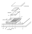
- Exploded view 6 around the semiconductor element 1 is an exploded view around the semiconductor element 1 (1A, 1B) of the semiconductor device 100 according to the first embodiment.
- a pattern wiring layer 21 is formed on the circuit board 2.
- a part or all of the pattern wiring layer 21 is used when each electrode of the semiconductor element 1 is connected to a terminal.
- electrodes (drain electrodes) 13 13 (13D1, 13D2) are formed on the surface on the circuit board 2 side. It is bonded to the pattern wiring layer 21 of the circuit board 2 via a solder (conductive bonding material) 53.
- Metal plates 4 (4A, 4B) are arranged.
- the metal plate 4 (4A, 4B) is provided with a convex portion 41 at a position corresponding to the main electrode (source electrode) 11 (11S1, 11S2).
- the convex portion 41 is provided on the main electrode (source electrode) 11 (11S1, 11S2) side.
- a layer of solder (conductive bonding material) 51 is formed between the main electrodes (source electrodes) 11 (11S1, 11S2) and the metal plates 4 (4A, 4B).
- a layer of solder (conductive bonding material) 52 is formed between the metal frame 31 and the metal plate 4 (4A, 4B).
- the sub-electrode (gate electrode) 12 (12G1, 12G2) is formed smaller than the main electrode (source electrode) 11 (11S1, 11S2) at a position away from the main electrode (source electrode) 11 (11S1, 11S2). ..
- the metal plates 4 (4A, 4B) are not arranged at positions facing the auxiliary electrodes (gate electrodes) 12 (12G1, 12G2).
- the semiconductor device (100-2, 100-3, ...) Or a modification according to another embodiment will be described, but it is used in FIGS. 1 to 6 to explain the semiconductor device 100 according to the first embodiment.
- the same code as the one used has the same meaning.
- the effects corresponding to the semiconductor devices (100-2, 100-3, %) Or modifications according to the following embodiments have the same effects.
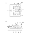
- FIG. 7 (A) and 7 (B) are diagrams for explaining the semiconductor device 100-2 according to the second embodiment.
- 7 (A) is a plan view
- FIG. 7 (B) is a cross-sectional view (a view showing the mold resin 6 omitted).
- the semiconductor device 100-2 according to the second embodiment basically has the same configuration as the semiconductor device 100 according to the first embodiment, but the configuration of the metal plate is different.
- the metal plate 4-2 has convex portions 41 and 42 on both surfaces. That is, in addition to having the convex portion 41 on the surface facing the main electrode (source electrode) 11, the convex portion 42 is also provided on the side where the metal frame 31 is located.
- the thickness t1 of the metal plate 4 is preferably equal to or less than the thickness t2 of the metal frame 31.
- solder (conductive bonding material) 52 between the metal frame 31 and the metal plate 4-2 is likely to gather around the convex portion 42, and a short circuit with the auxiliary electrode (gate electrode) 12 can be further suppressed.
- the upper portion of the convex portion 42 should be in the vicinity of the metal frame 31, and the lower portion of the convex portion 41 should be in the vicinity of the main electrode 11, that is, between the upper portion of the convex portion 42 and the lower portion of the convex portion 41.
- the distance t31 total thickness of the metal plate 4 in the thickness direction including the upper and lower convex portions 42 and 41
- the conductive bonding material (solder) 51 accurately joins the two by the convex portion 41 corresponding to the main electrode 11.
- the metal plate 4 and the metal frame 31 are joined by a conductive bonding material (solder) around the convex portion 42. ..
- the main electrode 11 and the metal frame 31 have a structure in which the conductive bonding materials (solders) 51 and 52 are gathered around the convex portions 41 and 42 by the metal plate 4 on which the convex portions 41 and 42 are formed, and the positions are accurate.
- the layer thicknesses of the conductive bonding materials 51 and 52 can be increased and made uniform.
- FIG. 8A is a diagram for explaining the semiconductor device 100-3 according to the third embodiment.
- FIG. 8A is a diagram for explaining the semiconductor device 100-3 according to the third embodiment in an enlarged manner around the semiconductor element 1.
- the semiconductor device 100-3 according to the third embodiment basically has the same configuration as the semiconductor device 100 according to the first embodiment, but has the shape of the main electrode (source electrode) 11-3 of the semiconductor element 1-3. , The composition of the metal plate 4-3 is different.
- the main electrodes (source electrodes) 11-3 of the semiconductor elements 1-3 are not divided into a plurality of regions, but are composed of one region. It has a rectangular shape.
- the metal plate 4-3 is arranged at a position corresponding to the main electrode (source electrode) 11-3, and has a rectangular shape similar to that of the main electrode (source electrode) 11-3.
- the convex portion 41 of the metal plate 4-3 is formed on the surface of the metal plate 4-3 on the main electrode (source electrode) 11-3 side. In the drawing, two convex portions 41 are formed in the lateral direction on the upper side and the lower side of the metal plate 4-3, and two convex portions 41 are formed in the central portion.
- the metal plate 4-3 can easily form the convex portion 41 at the position corresponding to the main electrode (source electrode) 11-3 side, and the position with the main electrode (source electrode) 11-3. It is easy to match.
- FIG. 8B is a diagram for explaining the semiconductor device 100-4 according to the fourth embodiment.
- FIG. 8B is a diagram for explaining the semiconductor device 100-4 according to the fourth embodiment by enlarging the periphery of the semiconductor element 1-4.
- the semiconductor device 100-4 according to the fourth embodiment basically has the same configuration as the semiconductor device 100 according to the first embodiment (semiconductor elements 1-4 are also the same as the semiconductor element 1), but the metal plate 4-4.
- the composition of is different.
- the metal plate 4-4 is rectangular and has no notch in the central portion, and two each for each of the four regions of the main electrode (source electrode) 11. The difference is that the convex portion 41 is formed at the same position in the region of.
- the bonding state of the solder (conductive bonding material) 51 between the main electrode (source electrode) 11 and the metal plate 4 in each of the four regions of the main electrode (source electrode) 11 becomes similar.
- the currents flowing through the four regions are equalized.
- FIG. 8C is a diagram for explaining the semiconductor device 100-5 according to the fifth embodiment.
- FIG. 8C is a diagram for explaining the semiconductor device 100-5 according to the fifth embodiment in an enlarged manner around the semiconductor element 1-5.
- the semiconductor device 100-5 according to the fifth embodiment basically has the same configuration as the semiconductor device 100 according to the first embodiment, but has the shape of the main electrode (source electrode) 11-5 of the semiconductor element 1-5. , The composition of the metal plate 4-5 is different.
- the main electrodes (source electrodes) 11-5 of the semiconductor element 1-5 are divided into a plurality of regions (four regions) as in the first embodiment.
- the length in the left-right direction is long, and the region close to the sub-electrode (gate electrode) 12 (two regions in the center on the figure).
- the length in the left-right direction is shortened by the distance from the auxiliary electrode (gate electrode) 12.
- the distance from the sub-electrode (gate electrode) 12 is almost the same as that of the four regions of the main electrode (source electrode) 11-5.
- the overall shape of the metal plate 4-5 is the same as the shape of the entire four regions of the main electrode (source electrode) 11-5, and the shape is along the entire four regions of the main electrode (source electrode) 11-5. ing.
- the convex portions 41 of the metal plate 4-5 are two in the left-right direction at the locations corresponding to the upper and lower regions of the main electrode (source electrode) 11-5, and one in the central portion at the locations corresponding to the two central regions. It is formed.
- the short circuit between the main electrode (source electrode) 11-5 and the sub electrode (gate electrode) 12 can be further suppressed.
- FIG. 9A is a diagram for explaining the semiconductor device 100-6 according to the sixth embodiment.
- FIG. 9A is a diagram for explaining the semiconductor device 100-6 according to the sixth embodiment in an enlarged manner around the semiconductor element 1-6.
- the semiconductor device 100-6 according to the sixth embodiment basically has the same configuration as the semiconductor device 100 according to the first embodiment, but has the shape of the main electrode (source electrode) 11-6 of the semiconductor element 1-6. , The composition of the metal plate 4-6 is different.
- the main electrode (source electrode) 11-6 of the semiconductor element 1-6 basically has four regions, but they are not independent and the semiconductor element. Patterned on the surface of 1-6. As shown in FIG. 9A, the main electrode (source electrode) 11-6 has four regions extending in the left-right direction in the up-down direction, which are connected to form a meandering shape.
- the overall shape of the metal plate 4-6 is a rectangular shape that substantially covers the entire main electrode (source electrode) 11-6.
- FIG. 9B is a diagram for explaining the semiconductor device 100-7 according to the seventh embodiment.
- FIG. 9B is a diagram for explaining the semiconductor device 100-7 according to the seventh embodiment in an enlarged manner around the semiconductor element 1.
- the semiconductor device 100-7 according to the seventh embodiment basically has the same configuration as the semiconductor device 100 according to the first embodiment, but has the shape of the main electrode (source electrode) 11-7 of the semiconductor element 1-7. , The composition of the metal plate 4-7 is different.
- the main electrode (source electrode) 11-7 of the semiconductor element 1-7 is divided into an upper two-thirds region and a lower one-third region. Since the upper two-thirds region is further divided into approximately two regions, it has approximately three regions in total.
- the main electrode (source electrode) 11-7 is formed at a distance so as to be away from the sub-electrode (gate electrode) 12. (Formed by retracting to the right).
- the overall shape of the metal plate 4-7 is a rectangular shape that almost covers the entire main electrode (source electrode) 11-7.
- the main electrode (source electrode) 11-7 is formed so as to be away from the sub-electrode (gate electrode) 12, the shape is the same as that of the main electrode (source electrode) 11-7.
- Two convex portions 41 of the metal plate 4-7 are formed in the upper region and two in the left-right direction in the lower region, and one in the central portion in the central region.
- the degree of freedom in the shape of the main electrode (source electrode) 11-7 is increased.
- FIG. 10A is a diagram for explaining the semiconductor device 100-86 according to the eighth embodiment.
- FIG. 10A is a diagram for explaining the semiconductor device 100-8 according to the eighth embodiment in an enlarged manner around the semiconductor element 1-8.
- the semiconductor device 100-8 according to the eighth embodiment basically has the same configuration as the semiconductor device 100 according to the first embodiment, but the electrodes (drain electrodes) 13-8 of the semiconductor elements 1-8 are mounted on the circuit board 2. It differs in that it is not formed on the side but is formed on the metal frame 31 side. That is, in the semiconductor device 100-8 according to the eighth embodiment, the main electrode (source electrode) 11-8, the electrode (drain electrode) 13-8, and the sub-electrode (gate) are placed on the metal frame 31 side of the semiconductor element 1-8. Electrode) 12 is formed. Since the electrodes 13-8 are formed on the surface facing the metal frame 31, they serve as “main electrodes", but here they are referred to as "electrodes (drain electrodes) 13-8".
- the main electrode (source electrode) 11-8 and the electrode (drain electrode) 13-8 are formed one by one (rectangular) with substantially the same size and shape.
- the metal plate 4-8A is arranged at a position corresponding to the main electrode (source electrode) 11-8, and the metal plate 4-8B is arranged at a position corresponding to the electrode (drain electrode) 13-8.
- the metal plates 4-8A and 4-8B are provided with convex portions 41 at positions corresponding to the main electrodes (source electrodes) 11-8 and the electrodes (drain electrodes) 13-8, respectively.
- the present invention can be applied even if the main electrode (source electrode) 11-8, the electrode (drain electrode) 13-8, and the sub-electrode (gate electrode) 12 are formed on one side of the semiconductor element. is there.
- FIG. 10B is a diagram for explaining the semiconductor device 100-9 according to the ninth embodiment.
- FIG. 10B is a diagram for explaining the semiconductor device 100-9 according to the ninth embodiment in an enlarged manner around the semiconductor element 1-9.
- the semiconductor device 100-9 according to the ninth embodiment basically has the same configuration as the semiconductor device 100 according to the first embodiment, but the electrodes (drain electrodes) 13-9 of the semiconductor elements 1-9 are mounted on the circuit board 2. It differs in that it is not formed on the side but is formed on the metal frame 31 side. That is, in the semiconductor device 100-9 according to the eighth embodiment, the main electrode (source electrode) 11-9, the electrode (drain electrode) 13-9, and the sub-electrode (gate) are placed on the metal frame 31 side of the semiconductor element 1-9. Electrode) 12 is formed. Since the electrodes 13-9 are formed on the surface facing the metal frame 31, they serve as “main electrodes", but here they are referred to as "electrodes (drain electrodes) 13-9".
- the main electrode (source electrode) 11-9 and the electrode (drain electrode) 13-9 each have a plurality of regions (two regions).
- the metal plate 4-9A is arranged at a position corresponding to the entire region (two regions) of the main electrode (source electrode) 11-9, and corresponds to the entire region (two regions) of the electrode (drain electrode) 13-9.
- a metal plate 4-9B is arranged at the position.
- the metal plates 4-9A and 4-9B are provided with convex portions 41 at positions corresponding to the main electrodes (source electrodes) 11-8 and the electrodes (drain electrodes) 13-8, respectively.
- the present invention can be applied even if the main electrode (source electrode) 11-9, the electrode (drain electrode) 13-9, and the sub-electrode (gate electrode) 12 are formed on one side of the semiconductor element. is there.
- FIG. 11 is a diagram for explaining the semiconductor device 100-10 according to the tenth embodiment.
- the semiconductor device 100-10 according to the tenth embodiment basically has the same configuration as the semiconductor device 100 according to the first embodiment, but the semiconductor device 100 according to the first embodiment has a semiconductor device 100 as shown in FIG.
- the circuit built in is composed of two semiconductor elements (1A, 1B), whereas the semiconductor device 100-10 of the tenth embodiment is different in that the same circuit is composed of one semiconductor element 1-10.
- the main electrode (source electrode) 11S1 is on the metal frame 31A (31B) side of the semiconductor element 1A (1B).
- (11S2) and the auxiliary electrode (gate electrode) 12G1 (12G2), and the electrode (drain electrode) 13D1 (13D2) on the opposite side are formed between the metal frame 31A (31B) and the main electrode (source electrode) 11S1 (11S2).
- a metal plate 4A (4B) having a convex portion 41 formed at a position corresponding to the main electrode (source electrode) 11S1 (11S2) is arranged, but in the semiconductor device 100-10 according to the tenth embodiment, one semiconductor element is provided.
- the main electrode (drain electrode) 13D1, the main electrode (source electrode) 11S2, and the auxiliary electrodes (gate electrodes) 12G1 and 12G2 are on the metal frame 31-10 side of the semiconductor element 1-10.
- a metal plate 4-10A having a convex portion 41 formed at a position corresponding to the main electrode (drain electrode) 13D1 is arranged between the metal frame 31-10 and the main electrode (drain electrode) 13D1 to form a metal frame.
- a metal plate 4-10B having a convex portion 41 formed at a position corresponding to the main electrode (source electrode) 11S2 was arranged between 31-10 and the main electrode (source electrode) 11S2.
- the material of the metal frame 31-10 is the same as that of the metal frame 31 of the semiconductor device 100 according to the first embodiment.
- the main electrode (drain electrode) 13D1 and the main electrode (source electrode) 11S2 were divided into four regions as shown in FIGS. 5 and 6.
- the metal plates 4-10A and 4-10B were also made of the same materials as in the first embodiment, and their shapes were the same as those shown in FIGS. 5 and 6.
- the wiring members 32-10A and 32-10B were the same as the wiring members 32 of the first embodiment (similar materials, joint structure with the gate electrode, etc., see FIG. 1 and the like).
- one semiconductor element 1-10 has a plurality of main electrodes (13D1, 11S2) on the metal frame 31-10 side, the respective main electrodes 13D1 and the metal frame 31-10 and the main electrodes are main. Since the semiconductor device 100 can be formed with a thick layer of conductive bonding material (51, 52) formed between the electrode 13S2 and the metal frame 31-10 with good positional accuracy, it can be connected to the weaker connection point of the semiconductor device 100-10. It is possible to provide a semiconductor device 100-10 having a low risk of failure due to a collection of loads (stress load, current load, etc.).
- FIG. 12A and 12 (B) are diagrams for explaining the semiconductor device 100-11 according to the eleventh embodiment.
- FIG. 12A is a diagram for explaining the circuit of the semiconductor device 100-11
- FIG. 12B is a diagram for explaining the internal structure of the semiconductor device 100-11.
- the semiconductor device 100-11 according to the eleventh embodiment basically has the same configuration as the semiconductor device 100 according to the first embodiment, but the semiconductor device 100 according to the first embodiment incorporates a transistor as shown in FIG.
- the semiconductor device 100-11 has a circuit having a built-in diode as shown in FIG. 12 (A) and a built-in diode as shown in FIG. 12 (B).
- the diode electrodes 15A1 and 15A2 formed on the metal frames 31-11A and 31-11B of the semiconductor element 1-11 both have substantially the same magnitude of the current. The difference is that it is an electrode through which
- the semiconductor device 100-11 has a semiconductor element 1-11 incorporating a diode 1D1 and a diode 1D2.
- the anode electrode 15A1 of the diode 1D1 is connected to the terminal 9A1, and the anode electrode 15A2 of the diode 1D2 is connected to the terminal 9A2.
- Both the cathode electrode 15C1 of the diode 1D1 and the cathode electrode 15C2 of the diode 1D2 are connected to the terminal 9C.
- the anode electrode 15A1 and the anode electrode 15A2 were formed on the metal frame 31-11A side of the semiconductor element 1-11, and the cathode electrode 15C1 (15C2) was formed on the opposite side. Since currents of substantially the same magnitude flow through the anode electrodes 15A1 and 15A2, one of them can be called a main electrode and the other can be called a sub-electrode.
- the anode electrode 15A1 is referred to as a main electrode
- the anode electrode 15A2 is referred to as a sub-electrode.
- a metal plate 4-11B having a convex portion 41 formed at a position corresponding to the sub-electrode (anode electrode) 15A2 was also arranged between the metal frame 31-11B and the sub-electrode (anode electrode) 15A2.
- the materials of the metal frames 31-11A and 31-11B are the same as those of the metal frame 31 of the semiconductor device 100 according to the first embodiment.
- the main electrode (anode electrode) 15A1 and the sub-electrode (anode electrode) 15A2 were divided into four regions as shown in FIGS. 5 and 6.
- the metal plates 4-11A and 4-11B were also made of the same materials as in the first embodiment, and their shapes were the same as those shown in FIGS. 5 and 6.
- the cathode electrodes 15C1 and 15C2 are connected on the surfaces opposite to the metal frames 31-11A and 31-11B of the semiconductor element 1-11 and are electrically the same electrodes.
- the main electrode 15A1 is supported between the metal frame 31-11A and the main electrode 15A1.
- the metal plate 4-11A on which the convex portion 41 is formed is formed at the position where the convex portion 41 is formed, but also the convex portion 41 is formed between the metal frame 31-11B and the auxiliary electrode 15A2 at a position corresponding to the auxiliary electrode 15A2.
- a thick layer of the conductive bonding material is formed between the main electrode 15A1 and the metal frame 31-11A and between the sub-electrode 15A2 and the metal frame 31-11B. It is possible to provide a semiconductor device that can withstand a large current and stress.
- the semiconductor device (100, 100-2, 7) Uses two of the semiconductor elements 1A and 1B shown in FIG. An embodiment of a semiconductor device in which one semiconductor element 1A is mounted instead of being mounted.
- the embodiment of the semiconductor device according to the tenth embodiment (see FIG. 11), wherein the main electrode and the metal plate (13D1 and 4-10A, 11S2 and 4-10B) are configured as follows.
- the configurations of the main electrode and the metal plate (15A1 and 4-11A) and the auxiliary electrode and the metal plate (15A2 and 4-11B) are as follows.
- Embodiment of a semiconductor device An embodiment of a semiconductor device as shown in the second embodiment shown in FIGS. 7A and 7B.
- FIG. 7B An embodiment of a semiconductor device in which the metal plate 4 has a convex portion 42 on the metal frame side instead of having the convex portion 41 on the main electrode 11 side.
- the first embodiment see FIGS. 1, 5, and 7
- the third embodiment see FIG. 8 (A)
- the fourth embodiment see FIG. 8 (B)
- the fifth embodiment see FIG. 8 (C)
- Embodiment 6 see FIG. 9 (A)
- embodiment 7 see FIG. 9 (B)
- embodiment 8 see FIG. 10 (A)
- embodiment 9 see FIG. 10 (B)
- FIG. 10 (B) Each of the tenth embodiment (see FIG. 11) and the eleventh embodiment (see FIG. 12B), instead of the metal plate 4 having the convex portion 41 on the main electrode 11 side, the convex portion 42 on the metal frame side. (See FIG. 7B).
- FIG. 7B An embodiment of a semiconductor device in which the metal plate 4 has a convex portion 41 on the main electrode 11 side and also has a convex portion 42 on the metal frame side.
- the first embodiment see FIGS. 1, 5, and 7
- the third embodiment see FIG. 8 (A)
- the fourth embodiment see FIG. 8 (B)
- the fifth embodiment see FIG. 8 (C)
- Embodiment 6 see FIG. 9 (A)
- embodiment 7 see FIG. 9 (B)
- embodiment 8 see FIG. 10 (A)
- embodiment 9 see FIG. 10 (B)
- FIG. 10 (B) Each of the tenth embodiment (see FIG. 11) and the eleventh embodiment (see FIG. 12B), the metal plate 4 has a convex portion 41 on the main electrode 11 side, and the convex portion 42 also on the metal frame side. (See FIG. 7B).
- a semiconductor device may be a semiconductor device in which a plurality of semiconductor elements 1 are used and connected in parallel or in series according to the rated specifications.
- the semiconductor element 1 in the embodiment may be a semiconductor device having a configuration in which switching elements such as MOSFETs and IGBTs, rectifying elements such as fast recovery diodes and Schottky barrier diodes, and control rectifiers such as thyristors are appropriately combined. ..
- Convex part, 42 ... Convex part, 51, 52, 53, 54 ... Solder (conductive bonding material), 81 ... Frame frame, 100, 100-2, 100-3, 100-4, 100-5, 100 -6, 100-7, 100-8, 100-9, 100-10, 100-11 ... Semiconductor device, 911, 913 ... Terminal, 941 ... Convex, 975 ... Conductive bonding material, 995 ... Semiconductor element, 999 ... Jigs
Landscapes
- Cooling Or The Like Of Semiconductors Or Solid State Devices (AREA)
- Structures Or Materials For Encapsulating Or Coating Semiconductor Devices Or Solid State Devices (AREA)
Priority Applications (6)
| Application Number | Priority Date | Filing Date | Title |
|---|---|---|---|
| PCT/JP2019/015603 WO2020208739A1 (ja) | 2019-04-10 | 2019-04-10 | 半導体装置 |
| PCT/JP2019/049098 WO2020208867A1 (ja) | 2019-04-10 | 2019-12-16 | 半導体装置 |
| US17/601,926 US11881444B2 (en) | 2019-04-10 | 2019-12-16 | Semiconductor device |
| CN201980094078.5A CN113574668B (zh) | 2019-04-10 | 2019-12-16 | 半导体装置 |
| JP2021513161A JP7301124B2 (ja) | 2019-04-10 | 2019-12-16 | 半導体装置 |
| NL2025200A NL2025200B1 (en) | 2019-04-10 | 2020-03-24 | Semiconductor device |
Applications Claiming Priority (1)
| Application Number | Priority Date | Filing Date | Title |
|---|---|---|---|
| PCT/JP2019/015603 WO2020208739A1 (ja) | 2019-04-10 | 2019-04-10 | 半導体装置 |
Publications (1)
| Publication Number | Publication Date |
|---|---|
| WO2020208739A1 true WO2020208739A1 (ja) | 2020-10-15 |
Family
ID=72750530
Family Applications (2)
| Application Number | Title | Priority Date | Filing Date |
|---|---|---|---|
| PCT/JP2019/015603 Ceased WO2020208739A1 (ja) | 2019-04-10 | 2019-04-10 | 半導体装置 |
| PCT/JP2019/049098 Ceased WO2020208867A1 (ja) | 2019-04-10 | 2019-12-16 | 半導体装置 |
Family Applications After (1)
| Application Number | Title | Priority Date | Filing Date |
|---|---|---|---|
| PCT/JP2019/049098 Ceased WO2020208867A1 (ja) | 2019-04-10 | 2019-12-16 | 半導体装置 |
Country Status (5)
| Country | Link |
|---|---|
| US (1) | US11881444B2 (https=) |
| JP (1) | JP7301124B2 (https=) |
| CN (1) | CN113574668B (https=) |
| NL (1) | NL2025200B1 (https=) |
| WO (2) | WO2020208739A1 (https=) |
Families Citing this family (7)
| Publication number | Priority date | Publication date | Assignee | Title |
|---|---|---|---|---|
| US20220020671A1 (en) * | 2020-07-20 | 2022-01-20 | Electronics And Telecommunications Research Institute | Flip-stack type semiconductor package and method of manufacturing the same |
| JP7404208B2 (ja) * | 2020-09-24 | 2023-12-25 | 株式会社東芝 | 半導体装置 |
| EP4213203B1 (en) * | 2022-01-12 | 2026-03-04 | Nexperia B.V. | Semiconductor device package and method for manufacturing the same |
| JP2023173191A (ja) * | 2022-05-25 | 2023-12-07 | ルネサスエレクトロニクス株式会社 | 半導体装置およびその製造方法 |
| US12500151B2 (en) | 2022-07-12 | 2025-12-16 | Littelfuse, Inc. | Solderless and pressure contact connection |
| US12308338B2 (en) * | 2022-07-14 | 2025-05-20 | Littelfuse, Inc. | Power substrate assembly with reduced warpage |
| JP2025014423A (ja) * | 2023-07-18 | 2025-01-30 | 株式会社東芝 | 半導体装置 |
Citations (4)
| Publication number | Priority date | Publication date | Assignee | Title |
|---|---|---|---|---|
| JP2008227131A (ja) * | 2007-03-13 | 2008-09-25 | Renesas Technology Corp | 半導体装置及びその製造方法 |
| JP2011249395A (ja) * | 2010-05-24 | 2011-12-08 | Mitsubishi Electric Corp | 半導体装置 |
| JP2012069703A (ja) * | 2010-09-22 | 2012-04-05 | Toshiba Corp | 半導体モジュール及び半導体モジュールの製造方法 |
| JP2017034152A (ja) * | 2015-08-04 | 2017-02-09 | 三菱電機株式会社 | 電力用半導体装置 |
Family Cites Families (12)
| Publication number | Priority date | Publication date | Assignee | Title |
|---|---|---|---|---|
| JPS60108084A (ja) | 1983-11-17 | 1985-06-13 | シャープ株式会社 | 洗濯機の制御方法 |
| JP2005136018A (ja) * | 2003-10-29 | 2005-05-26 | Denso Corp | 半導体装置 |
| JP4764692B2 (ja) * | 2005-09-29 | 2011-09-07 | 日立オートモティブシステムズ株式会社 | 半導体モジュール |
| JP2007184525A (ja) * | 2005-12-07 | 2007-07-19 | Mitsubishi Electric Corp | 電子機器装置 |
| JP2008153432A (ja) * | 2006-12-18 | 2008-07-03 | Renesas Technology Corp | 半導体装置およびその製造方法 |
| JP5473733B2 (ja) * | 2010-04-02 | 2014-04-16 | 株式会社日立製作所 | パワー半導体モジュール |
| JP2015005681A (ja) * | 2013-06-24 | 2015-01-08 | 三菱電機株式会社 | 半導体装置及びその製造方法 |
| CN104779228B (zh) * | 2015-04-14 | 2018-09-28 | 天津大学 | 一种功率半导体模块三维封装的结构和方法 |
| EP3702072A1 (en) * | 2015-09-07 | 2020-09-02 | Hitachi Chemical Company, Ltd. | Copper paste for joining, method for manufacturing joined body, and method for manufacturing semiconductor device |
| JP2017112280A (ja) * | 2015-12-17 | 2017-06-22 | トヨタ自動車株式会社 | 半導体モジュール |
| DE112017002198T5 (de) * | 2016-04-26 | 2019-01-10 | Mitsubishi Electric Corporation | Halbleitereinrichtung |
| CN110214372B (zh) | 2017-02-20 | 2023-08-01 | 新电元工业株式会社 | 电子装置以及连接体 |
-
2019
- 2019-04-10 WO PCT/JP2019/015603 patent/WO2020208739A1/ja not_active Ceased
- 2019-12-16 CN CN201980094078.5A patent/CN113574668B/zh active Active
- 2019-12-16 US US17/601,926 patent/US11881444B2/en active Active
- 2019-12-16 JP JP2021513161A patent/JP7301124B2/ja active Active
- 2019-12-16 WO PCT/JP2019/049098 patent/WO2020208867A1/ja not_active Ceased
-
2020
- 2020-03-24 NL NL2025200A patent/NL2025200B1/en active
Patent Citations (4)
| Publication number | Priority date | Publication date | Assignee | Title |
|---|---|---|---|---|
| JP2008227131A (ja) * | 2007-03-13 | 2008-09-25 | Renesas Technology Corp | 半導体装置及びその製造方法 |
| JP2011249395A (ja) * | 2010-05-24 | 2011-12-08 | Mitsubishi Electric Corp | 半導体装置 |
| JP2012069703A (ja) * | 2010-09-22 | 2012-04-05 | Toshiba Corp | 半導体モジュール及び半導体モジュールの製造方法 |
| JP2017034152A (ja) * | 2015-08-04 | 2017-02-09 | 三菱電機株式会社 | 電力用半導体装置 |
Also Published As
| Publication number | Publication date |
|---|---|
| CN113574668A (zh) | 2021-10-29 |
| JP7301124B2 (ja) | 2023-06-30 |
| WO2020208867A1 (ja) | 2020-10-15 |
| JPWO2020208867A1 (https=) | 2020-10-15 |
| CN113574668B (zh) | 2024-06-14 |
| US11881444B2 (en) | 2024-01-23 |
| NL2025200A (en) | 2020-10-15 |
| NL2025200B1 (en) | 2021-04-14 |
| US20220148946A1 (en) | 2022-05-12 |
Similar Documents
| Publication | Publication Date | Title |
|---|---|---|
| WO2020208739A1 (ja) | 半導体装置 | |
| US8736043B2 (en) | Power device having a specific range of distances between collector and emitter electrodes | |
| KR101614669B1 (ko) | 전력용 반도체 장치 | |
| CN104919589A (zh) | 半导体装置 | |
| CN108352380A (zh) | 功率半导体装置 | |
| JPWO2020071185A1 (ja) | 半導体装置および半導体装置の製造方法 | |
| CN112786556B (zh) | 半导体装置及半导体装置的制造方法 | |
| JP2007234690A (ja) | パワー半導体モジュール | |
| CN108538825B (zh) | 功率模块 | |
| JP2020170736A (ja) | 半導体装置 | |
| JP7795476B2 (ja) | 半導体装置 | |
| JP5652346B2 (ja) | パワー半導体モジュール | |
| JP2015115471A (ja) | 電力用半導体装置 | |
| WO2022075003A1 (ja) | 半導体装置 | |
| WO2022259824A1 (ja) | 接合構造および半導体装置 | |
| JP5869285B2 (ja) | 半導体装置 | |
| JP6919392B2 (ja) | 半導体モジュール | |
| JP2017123360A (ja) | 半導体モジュール | |
| JP2019083292A (ja) | 半導体装置 | |
| WO2020153190A1 (ja) | 半導体モジュールおよびac/dcコンバータユニット | |
| JP2004221381A (ja) | 半導体装置 | |
| JP2021068859A (ja) | 半導体モジュール | |
| TW201721830A (zh) | 電動馬達用的功率模組 | |
| JP2017079307A (ja) | 半導体装置および半導体装置の製造方法 | |
| JP7392308B2 (ja) | 半導体装置 |
Legal Events
| Date | Code | Title | Description |
|---|---|---|---|
| 121 | Ep: the epo has been informed by wipo that ep was designated in this application |
Ref document number: 19924392 Country of ref document: EP Kind code of ref document: A1 |
|
| NENP | Non-entry into the national phase |
Ref country code: DE |
|
| 122 | Ep: pct application non-entry in european phase |
Ref document number: 19924392 Country of ref document: EP Kind code of ref document: A1 |
|
| NENP | Non-entry into the national phase |
Ref country code: JP |