WO2020184053A1 - 半導体装置 - Google Patents
半導体装置 Download PDFInfo
- Publication number
- WO2020184053A1 WO2020184053A1 PCT/JP2020/005573 JP2020005573W WO2020184053A1 WO 2020184053 A1 WO2020184053 A1 WO 2020184053A1 JP 2020005573 W JP2020005573 W JP 2020005573W WO 2020184053 A1 WO2020184053 A1 WO 2020184053A1
- Authority
- WO
- WIPO (PCT)
- Prior art keywords
- main
- width
- terminal
- main terminal
- sealing resin
- Prior art date
- Legal status (The legal status is an assumption and is not a legal conclusion. Google has not performed a legal analysis and makes no representation as to the accuracy of the status listed.)
- Ceased
Links
Images





Classifications
-
- H—ELECTRICITY
- H10—SEMICONDUCTOR DEVICES; ELECTRIC SOLID-STATE DEVICES NOT OTHERWISE PROVIDED FOR
- H10W—GENERIC PACKAGES, INTERCONNECTIONS, CONNECTORS OR OTHER CONSTRUCTIONAL DETAILS OF DEVICES COVERED BY CLASS H10
- H10W40/00—Arrangements for thermal protection or thermal control
- H10W40/70—Fillings or auxiliary members in containers or in encapsulations for thermal protection or control
- H10W40/77—Auxiliary members characterised by their shape
- H10W40/778—Auxiliary members characterised by their shape in encapsulations
-
- H—ELECTRICITY
- H10—SEMICONDUCTOR DEVICES; ELECTRIC SOLID-STATE DEVICES NOT OTHERWISE PROVIDED FOR
- H10W—GENERIC PACKAGES, INTERCONNECTIONS, CONNECTORS OR OTHER CONSTRUCTIONAL DETAILS OF DEVICES COVERED BY CLASS H10
- H10W40/00—Arrangements for thermal protection or thermal control
- H10W40/20—Arrangements for cooling
- H10W40/25—Arrangements for cooling characterised by their materials
- H10W40/255—Arrangements for cooling characterised by their materials having a laminate or multilayered structure, e.g. direct bond copper [DBC] ceramic substrates
-
- H—ELECTRICITY
- H10—SEMICONDUCTOR DEVICES; ELECTRIC SOLID-STATE DEVICES NOT OTHERWISE PROVIDED FOR
- H10W—GENERIC PACKAGES, INTERCONNECTIONS, CONNECTORS OR OTHER CONSTRUCTIONAL DETAILS OF DEVICES COVERED BY CLASS H10
- H10W40/00—Arrangements for thermal protection or thermal control
- H10W40/40—Arrangements for thermal protection or thermal control involving heat exchange by flowing fluids
- H10W40/47—Arrangements for thermal protection or thermal control involving heat exchange by flowing fluids by flowing liquids, e.g. forced water cooling
-
- H—ELECTRICITY
- H10—SEMICONDUCTOR DEVICES; ELECTRIC SOLID-STATE DEVICES NOT OTHERWISE PROVIDED FOR
- H10W—GENERIC PACKAGES, INTERCONNECTIONS, CONNECTORS OR OTHER CONSTRUCTIONAL DETAILS OF DEVICES COVERED BY CLASS H10
- H10W70/00—Package substrates; Interposers; Redistribution layers [RDL]
- H10W70/40—Leadframes
- H10W70/461—Leadframes specially adapted for cooling
-
- H—ELECTRICITY
- H10—SEMICONDUCTOR DEVICES; ELECTRIC SOLID-STATE DEVICES NOT OTHERWISE PROVIDED FOR
- H10W—GENERIC PACKAGES, INTERCONNECTIONS, CONNECTORS OR OTHER CONSTRUCTIONAL DETAILS OF DEVICES COVERED BY CLASS H10
- H10W70/00—Package substrates; Interposers; Redistribution layers [RDL]
- H10W70/40—Leadframes
- H10W70/464—Additional interconnections in combination with leadframes
- H10W70/468—Circuit boards
-
- H—ELECTRICITY
- H10—SEMICONDUCTOR DEVICES; ELECTRIC SOLID-STATE DEVICES NOT OTHERWISE PROVIDED FOR
- H10W—GENERIC PACKAGES, INTERCONNECTIONS, CONNECTORS OR OTHER CONSTRUCTIONAL DETAILS OF DEVICES COVERED BY CLASS H10
- H10W70/00—Package substrates; Interposers; Redistribution layers [RDL]
- H10W70/40—Leadframes
- H10W70/481—Leadframes for devices being provided for in groups H10D8/00 - H10D48/00
-
- H—ELECTRICITY
- H10—SEMICONDUCTOR DEVICES; ELECTRIC SOLID-STATE DEVICES NOT OTHERWISE PROVIDED FOR
- H10W—GENERIC PACKAGES, INTERCONNECTIONS, CONNECTORS OR OTHER CONSTRUCTIONAL DETAILS OF DEVICES COVERED BY CLASS H10
- H10W72/00—Interconnections or connectors in packages
-
- H—ELECTRICITY
- H10—SEMICONDUCTOR DEVICES; ELECTRIC SOLID-STATE DEVICES NOT OTHERWISE PROVIDED FOR
- H10W—GENERIC PACKAGES, INTERCONNECTIONS, CONNECTORS OR OTHER CONSTRUCTIONAL DETAILS OF DEVICES COVERED BY CLASS H10
- H10W90/00—Package configurations
-
- H—ELECTRICITY
- H10—SEMICONDUCTOR DEVICES; ELECTRIC SOLID-STATE DEVICES NOT OTHERWISE PROVIDED FOR
- H10W—GENERIC PACKAGES, INTERCONNECTIONS, CONNECTORS OR OTHER CONSTRUCTIONAL DETAILS OF DEVICES COVERED BY CLASS H10
- H10W90/00—Package configurations
- H10W90/811—Multiple chips on leadframes
-
- H—ELECTRICITY
- H10—SEMICONDUCTOR DEVICES; ELECTRIC SOLID-STATE DEVICES NOT OTHERWISE PROVIDED FOR
- H10W—GENERIC PACKAGES, INTERCONNECTIONS, CONNECTORS OR OTHER CONSTRUCTIONAL DETAILS OF DEVICES COVERED BY CLASS H10
- H10W40/00—Arrangements for thermal protection or thermal control
- H10W40/20—Arrangements for cooling
- H10W40/22—Arrangements for cooling characterised by their shape, e.g. having conical or cylindrical projections
-
- H—ELECTRICITY
- H10—SEMICONDUCTOR DEVICES; ELECTRIC SOLID-STATE DEVICES NOT OTHERWISE PROVIDED FOR
- H10W—GENERIC PACKAGES, INTERCONNECTIONS, CONNECTORS OR OTHER CONSTRUCTIONAL DETAILS OF DEVICES COVERED BY CLASS H10
- H10W70/00—Package substrates; Interposers; Redistribution layers [RDL]
- H10W70/40—Leadframes
- H10W70/421—Shapes or dispositions
-
- H—ELECTRICITY
- H10—SEMICONDUCTOR DEVICES; ELECTRIC SOLID-STATE DEVICES NOT OTHERWISE PROVIDED FOR
- H10W—GENERIC PACKAGES, INTERCONNECTIONS, CONNECTORS OR OTHER CONSTRUCTIONAL DETAILS OF DEVICES COVERED BY CLASS H10
- H10W72/00—Interconnections or connectors in packages
- H10W72/071—Connecting or disconnecting
- H10W72/073—Connecting or disconnecting of die-attach connectors
- H10W72/07351—Connecting or disconnecting of die-attach connectors characterised by changes in properties of the die-attach connectors during connecting
- H10W72/07354—Connecting or disconnecting of die-attach connectors characterised by changes in properties of the die-attach connectors during connecting changes in dispositions
-
- H—ELECTRICITY
- H10—SEMICONDUCTOR DEVICES; ELECTRIC SOLID-STATE DEVICES NOT OTHERWISE PROVIDED FOR
- H10W—GENERIC PACKAGES, INTERCONNECTIONS, CONNECTORS OR OTHER CONSTRUCTIONAL DETAILS OF DEVICES COVERED BY CLASS H10
- H10W72/00—Interconnections or connectors in packages
- H10W72/30—Die-attach connectors
- H10W72/341—Dispositions of die-attach connectors, e.g. layouts
- H10W72/347—Dispositions of multiple die-attach connectors
-
- H—ELECTRICITY
- H10—SEMICONDUCTOR DEVICES; ELECTRIC SOLID-STATE DEVICES NOT OTHERWISE PROVIDED FOR
- H10W—GENERIC PACKAGES, INTERCONNECTIONS, CONNECTORS OR OTHER CONSTRUCTIONAL DETAILS OF DEVICES COVERED BY CLASS H10
- H10W72/00—Interconnections or connectors in packages
- H10W72/851—Dispositions of multiple connectors or interconnections
- H10W72/874—On different surfaces
- H10W72/884—Die-attach connectors and bond wires
-
- H—ELECTRICITY
- H10—SEMICONDUCTOR DEVICES; ELECTRIC SOLID-STATE DEVICES NOT OTHERWISE PROVIDED FOR
- H10W—GENERIC PACKAGES, INTERCONNECTIONS, CONNECTORS OR OTHER CONSTRUCTIONAL DETAILS OF DEVICES COVERED BY CLASS H10
- H10W72/00—Interconnections or connectors in packages
- H10W72/90—Bond pads, in general
- H10W72/921—Structures or relative sizes of bond pads
- H10W72/926—Multiple bond pads having different sizes
-
- H—ELECTRICITY
- H10—SEMICONDUCTOR DEVICES; ELECTRIC SOLID-STATE DEVICES NOT OTHERWISE PROVIDED FOR
- H10W—GENERIC PACKAGES, INTERCONNECTIONS, CONNECTORS OR OTHER CONSTRUCTIONAL DETAILS OF DEVICES COVERED BY CLASS H10
- H10W74/00—Encapsulations, e.g. protective coatings
- H10W74/10—Encapsulations, e.g. protective coatings characterised by their shape or disposition
- H10W74/111—Encapsulations, e.g. protective coatings characterised by their shape or disposition the semiconductor body being completely enclosed
-
- H—ELECTRICITY
- H10—SEMICONDUCTOR DEVICES; ELECTRIC SOLID-STATE DEVICES NOT OTHERWISE PROVIDED FOR
- H10W—GENERIC PACKAGES, INTERCONNECTIONS, CONNECTORS OR OTHER CONSTRUCTIONAL DETAILS OF DEVICES COVERED BY CLASS H10
- H10W90/00—Package configurations
- H10W90/701—Package configurations characterised by the relative positions of pads or connectors relative to package parts
- H10W90/731—Package configurations characterised by the relative positions of pads or connectors relative to package parts of die-attach connectors
- H10W90/736—Package configurations characterised by the relative positions of pads or connectors relative to package parts of die-attach connectors between a chip and a stacked lead frame, conducting package substrate or heat sink
-
- H—ELECTRICITY
- H10—SEMICONDUCTOR DEVICES; ELECTRIC SOLID-STATE DEVICES NOT OTHERWISE PROVIDED FOR
- H10W—GENERIC PACKAGES, INTERCONNECTIONS, CONNECTORS OR OTHER CONSTRUCTIONAL DETAILS OF DEVICES COVERED BY CLASS H10
- H10W90/00—Package configurations
- H10W90/701—Package configurations characterised by the relative positions of pads or connectors relative to package parts
- H10W90/751—Package configurations characterised by the relative positions of pads or connectors relative to package parts of bond wires
- H10W90/756—Package configurations characterised by the relative positions of pads or connectors relative to package parts of bond wires between a chip and a stacked lead frame, conducting package substrate or heat sink
Definitions
- This disclosure relates to semiconductor devices.
- Patent Document 1 proposes a semiconductor device.
- the semiconductor device includes a semiconductor element having a first main electrode and a second main electrode, a sealing resin body for sealing the semiconductor element, and a main terminal (terminal portion) electrically connected to the corresponding main electrode. ing.
- the semiconductor device of Patent Document 1 has one main terminal connected to the first main electrode and one second main terminal connected to the second main electrode as main terminals. Further reduction of inductance is required.
- An object of the present disclosure is to provide a semiconductor device capable of suppressing a temperature rise of a main terminal while reducing an inductance.
- the semiconductor device encloses at least one semiconductor element having a second main electrode through which a main current flows between the first main electrode and the first main electrode as a main electrode, and the semiconductor element.
- a plurality of main terminals electrically connected to the sealing resin body and the corresponding main electrode inside the sealing resin body and extended to the outside of the sealing resin body for connection with other members. It is provided with a first main terminal electrically connected to the first main electrode and a second main terminal electrically connected to the second main electrode.
- All main terminals protrude from one side of the sealing resin body.
- the first main terminal and the second main terminal are alternately arranged so that the side surfaces face each other in one direction orthogonal to the thickness direction of the semiconductor element, and the width of the protruding portion of the main terminal in one direction is sealed.
- the external connection portion to which other members are connected is wider than the boundary portion with the resin body.
- the first main terminal and the second main terminal are alternately arranged so that the side surfaces face each other.
- a plurality of pairs of side surfaces of a first main terminal and a second main terminal facing each other are formed. Thereby, the inductance can be reduced.
- the width of the area where all the terminals are arranged is less than the width of one surface at the boundary portion.
- the main terminal extends in a direction orthogonal to one direction over the inside and outside of the sealing resin body.
- the ratio of the gap between the terminals increases. Since the energized region of the main terminal becomes smaller, for example, it becomes difficult for DC current to flow, and there is a concern that the main terminal may be affected by the temperature rise due to energization.
- the DC current is a current that flows at a steady state when the semiconductor element is on.
- the width of the external connection portion is wider than the width of the boundary portion in the protruding portion of the main terminal.
- the energizing region of the main terminal is large. Further, outside the sealing resin body, the heat dissipation area by the main terminal is increased. Therefore, the temperature rise of the main terminal can be suppressed.
- FIG. 1 is a diagram showing a schematic configuration of a power conversion device to which the semiconductor device of the first embodiment is applied.
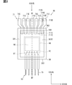
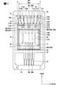
- FIG. 2 is a plan view showing a semiconductor device.
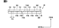
- FIG. 3 is a plan view of FIG. 2 as viewed from the A direction.
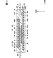
- FIG. 4 is a cross-sectional view taken along the line VV of FIG.
- FIG. 5 is an enlarged view of the periphery of the main terminal in FIG.
- FIG. 6 is a diagram showing the relationship between the number of main terminals, the inductance, and the terminal temperature in the reference example.
- FIG. 7 is a diagram showing a proximity effect.
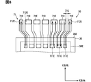
- FIG. 8 is an enlarged view of the periphery of the main terminal in the semiconductor device of the second embodiment.
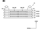
- FIG. 9 is a plan view showing a semiconductor module and a laminate.
- FIG. 10 is an enlarged view of the periphery of the main terminal in the semiconductor module provided with the semiconductor device of the third embodiment.
- FIG. 11 is a diagram showing a semiconductor device of the fourth embodiment.
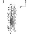
- FIG. 12 is a cross-sectional view taken along the line VII-VII of FIG.
- FIG. 13 is a cross-sectional view taken along the line VIII-VIII of FIG.
- FIG. 14 is an enlarged view of the region XIV shown in FIG.
- the thickness direction of the semiconductor element is referred to as the Z direction
- one direction orthogonal to the Z direction is referred to as the X direction
- a direction orthogonal to both the Z direction and the X direction is indicated as the Y direction.
- the shape along the XY plane defined by the X direction and the Y direction described above is defined as a planar shape.
- the power conversion device 1 shown in FIG. 1 is mounted on, for example, an electric vehicle or a hybrid vehicle.
- the power conversion device 1 performs power conversion between the DC power supply 2 and the motor generator 3.
- the DC power supply 2 is a rechargeable secondary battery such as a lithium ion battery or a nickel hydrogen battery.
- the motor generator 3 is a rotary electric machine of a three-phase AC system.
- the motor generator 3 functions as a traveling drive source of the vehicle, that is, an electric motor.
- the motor generator 3 functions as a generator during regeneration.
- the power converter 1 has a smoothing capacitor 4 and an inverter 5 which is a power converter.
- the positive electrode side terminal of the smoothing capacitor 4 is connected to the positive electrode which is the electrode on the high potential side of the DC power supply 2, and the negative electrode side terminal is connected to the negative electrode which is the electrode on the low potential side of the DC power supply 2.
- the inverter 5 converts the input DC power into a three-phase AC having a predetermined frequency and outputs it to the motor generator 3.
- the inverter 5 converts the AC power generated by the motor generator 3 into DC power.
- the inverter 5 is a DC-AC converter.
- the inverter 5 is configured to include a three-phase upper and lower arm circuit 6.
- a high potential power supply line 7 which is a power supply line on the positive electrode side
- a low potential power supply line 8 which is a power supply line on the negative electrode side.
- the connection points between the upper arm and the lower arm are connected to the output line 9 to the motor generator 3.
- an n-channel type insulated gate bipolar transistor 6i (hereinafter referred to as an IGBT 6i) is adopted as a switching element constituting each arm.
- FWD6d which is a diode for reflux, is connected to each of the IGBTs 6i in antiparallel.
- the upper and lower arm circuits 6 for one phase are configured to have two IGBTs 6i.
- the collector electrode of the IGBT 6i is connected to the high potential power supply line 7.
- the emitter electrode of the IGBT 6i is connected to the low potential power supply line 8. Then, the emitter electrode of the IGBT 6i in the upper arm and the collector electrode of the IGBT 6i in the lower arm are connected to each other.
- the power conversion device 1 may include a converter which is a power converter different from the inverter 5, a drive circuit of the inverter 5 and switching elements constituting the converter, and the like.
- the converter is a DC-DC converter that converts a DC voltage into a DC voltage having a different value.
- the semiconductor device 20 includes a sealing resin body 30, a semiconductor element 40, a heat sink 50, a terminal 60, and a lead frame 70 including a main terminal 71 and a signal terminal 73. There is. In FIG. 4, the main terminal 71E is also shown for convenience.
- the sealing resin body 30 seals a part of other elements constituting the semiconductor device 20. The rest of the other elements are exposed to the outside of the sealing resin body 30.
- the sealing resin body 30 seals, for example, the semiconductor element 40.
- the sealing resin body 30 seals a connecting portion formed between other elements constituting the semiconductor device 20.
- the sealing resin body 30 seals the connection portion between the semiconductor element 40 and the heat sink 50.
- the sealing resin body 30 seals the connection portion between the semiconductor element 40 and the terminal 60.
- the sealing resin body 30 seals the connection portion between the terminal 60 and the heat sink 50.
- the sealing resin body 30 seals the connection portion between the heat sink 50 and the main terminal 71.
- the sealing resin body 30 is made of, for example, an epoxy resin.
- the sealing resin body 30 is molded by, for example, a transfer molding method.
- the sealing resin body 30 may be referred to as a mold resin.
- the sealing resin body 30 has one side surface 300 and a back surface 301 opposite to the one side surface 300 in the Z direction.
- the front surface 300 and the back surface 301 are, for example, flat surfaces.
- the sealing resin body 30 has a side surface connecting the front surface 300 and the back surface 301. As shown in FIG. 2, the sealing resin body 30 of the present embodiment has a substantially rectangular shape in a plane.
- the sealing resin body 30 has a side surface 302 on which the main terminal 71 projects to the outside and a side surface 303 on which the signal terminal 73 projects to the outside.
- the side surface 303 is a surface opposite to the side surface 302 in the Y direction.
- the semiconductor element 40 is formed by forming an element on a semiconductor substrate such as Si, SiC, or GaN.
- the semiconductor device 20 includes at least one semiconductor element 40.
- the semiconductor element 40 has a gate electrode and a main electrode 41 through which a main current flows.
- the semiconductor element 40 constitutes one of the above-mentioned arms.
- the semiconductor element 40 is sometimes referred to as a semiconductor chip.
- the above-mentioned IGBT 6i and FWD 6d are formed on the semiconductor substrate.
- RC (Reverse Conducting) -IGBT is adopted as the semiconductor element 40.
- the elements formed on the semiconductor substrate have a vertical structure so that the main current flows in the Z direction.
- the gate electrode has, for example, a trench structure.
- the semiconductor element 40 has main electrodes on both sides in its thickness direction, that is, in the Z direction.
- the collector electrode 41C is provided on one side, and the emitter electrode 41E is provided on the back surface opposite to one side.
- the collector electrode 41C also serves as the cathode electrode of the FWD 6d.
- the emitter electrode 41E also serves as an anode electrode of the FWD 6d.
- the collector electrode 41C is formed on almost the entire surface of one surface.
- the emitter electrode 41E is formed on a part of the back surface.
- the collector electrode 41C corresponds to the first main electrode, and the emitter electrode 41E corresponds to the second main electrode.
- the semiconductor element 40 has a pad 42, which is an electrode for signals, on the forming surface of the emitter electrode 41E.
- the pad 42 is formed at a position different from that of the emitter electrode 41E.
- the pad 42 is electrically separated from the emitter electrode 41E.
- the semiconductor element 40 has a substantially rectangular shape in a plane.
- the pad 42 is formed at an end portion of the emitter electrode 41E opposite to the forming region in the Y direction.
- the semiconductor element 40 has, for example, five pads 42.
- the pad 42 has a gate electrode, a potential detection of the emitter electrode 41E, a current sense, and a temperature detection of the semiconductor element 40.
- the pad 42 for temperature detection includes an anode potential and a cathode potential of a temperature sensitive diode which is a temperature detection element.
- the five pads 42 are formed side by side in the X direction.
- an Al-based material can be used as a constituent material of electrodes such as the main electrode 41 and the pad 42.
- Cu When joining by solder or the like, it is preferable to contain Cu as a material.
- AlCuSi can be used.
- the heat sink 50 is arranged so as to sandwich the semiconductor element 40 in the Z direction.
- the heat sink 50 functions to dissipate at least the heat generated by the semiconductor element 40. Therefore, the heat sink 50 may be referred to as a heat radiating member.
- the heat sink 50 of the present embodiment also functions as wiring for electrically connecting the semiconductor element 40 and the main terminal 71.
- the heat sink 50 constitutes the main circuit of the inverter 5. Therefore, the heat sink 50 may be referred to as a wiring member.
- the heat sink 50 for example, a metal plate, a composite material of an electric insulator such as resin or ceramics, and a metal body can be adopted.
- the same type of member may be used for the heat sink 50C and the heat sink 50E, or different members may be used.
- the heat sink 50 is formed by using a metal plate containing Cu.
- the heat sinks 50 are provided in pairs so as to sandwich the semiconductor element 40.
- the semiconductor device 20 has a heat sink 50C arranged on the collector electrode 41C side and a heat sink 50E arranged on the emitter electrode 41E side as a pair of heat sinks 50.
- the heat sink 50 corresponds to a heat radiating member.
- the heat sink 50C corresponds to the first heat radiating member, and the heat sink 50E corresponds to the second heat radiating member.
- the heat sinks 50C and 50E are provided so as to include the semiconductor element 40 in a plan view from the Z direction.
- the heat sink 50C has a mounting surface 500C on the semiconductor element 40 side and a heat dissipation surface 501C opposite to the mounting surface 500C in the Z direction.
- the heat sink 50E has a mounting surface 500E and a heat radiating surface 501E.
- the mounting surfaces 500C and 500E face each other in the Z direction.
- the mounting surfaces 500C and 500E are substantially parallel to each other.
- the heat sinks 50C and 50E of the present embodiment have a substantially rectangular shape in a plane.
- the heat sinks 50C and 50E have substantially the same shape and size as each other.
- the heat sinks 50C and 50E are arranged so as to substantially coincide with each other in a plan view from the Z direction.
- each of the heat sinks 50C and 50E is sealed by the sealing resin body 30.
- the heat dissipation surface 501C of the heat sink 50C is exposed from the sealing resin body 30.
- the heat dissipation surface 501C is substantially flush with the surface 300.
- a portion of the surface of the heat sink 50C, excluding the connection portion with the collector electrode 41C, the heat dissipation surface 501C, and the connection portion with the corresponding main terminal 71C, is covered with the sealing resin body 30.
- the heat radiating surface 501E of the heat sink 50E is exposed from the sealing resin body 30.
- the heat radiating surface 501E is substantially flush with the back surface 301.
- the portion of the surface of the heat sink 50E excluding the connection portion with the terminal 60, the heat dissipation surface 501E, and the connection portion with the corresponding main terminal 71E is covered with the sealing resin body 30.
- the collector electrode 41C of the semiconductor element 40 is connected to the mounting surface 500C of the heat sink 50C via the joining member 80.
- a terminal 60 is connected to the mounting surface 500E of the heat sink 50E via a joining member 80.
- a conductive paste containing solder, Ag, or the like can be used as the joining member 80. In this embodiment, solder is used as the joining member 80.
- the terminal 60 functions as a wiring that electrically connects the emitter electrode 41E and the heat sink 50E.
- the terminal 60 functions to dissipate the heat generated by the semiconductor element 40.
- the terminal 60 is formed by using a material having excellent conductivity and thermal conductivity, for example, a metal material such as Cu.
- the terminal 60 is provided so as to substantially coincide with the emitter electrode 41E in a plan view in the Z direction.
- the terminal 60 has a substantially rectangular parallelepiped shape.
- the emitter electrode 41E of the semiconductor element 40 is connected to the surface opposite to the connection surface with the heat sink 50E via the bonding member 80.
- the lead frame 70 has a main terminal 71 and a signal terminal 73 as external connection terminals.
- the lead frame 70 is configured as a separate member from the heat sink 50.
- the lead frame 70 is formed by processing a metal plate made of Cu or the like by a press or the like.
- the main terminal 71 is an external connection terminal through which the main current flows.
- the lead frame 70 has a plurality of main terminals 71.
- the main terminal 71 is electrically connected to the corresponding main electrode of the semiconductor element 40.
- the semiconductor device 20 has a main terminal 71C corresponding to the collector electrode 41C and a main terminal 71E corresponding to the emitter electrode 41E as the main terminal 71.
- the main terminal 71C corresponds to the first main terminal, and the main terminal 71E corresponds to the second main terminal.
- the main terminal 71C is sometimes referred to as a collector terminal.
- the main terminal 71E is sometimes referred to as an emitter terminal.
- Each of the main terminals 71 extends inside and outside the sealing resin body 30.
- the main terminal 71 extends from the inside of the sealing resin body 30 in the Y direction and in a direction away from the semiconductor element 40. All the main terminals 71 project outward from the side surface 302 of the sealing resin body 30. At least the protruding portions of the main terminal 71 are aligned in the X direction. Details of the main terminal 71 will be described later.
- the signal terminal 73 is connected to the pad 42 of the corresponding semiconductor element 40.
- the lead frame 70 has a plurality of signal terminals 73.
- the signal terminal 73 is connected to the pad 42 inside the sealing resin body 30.
- the five signal terminals 73 connected to the pads 42 extend in the Y direction and away from the semiconductor element 40, respectively.
- the signal terminals 73 are arranged side by side in the X direction. All signal terminals 73 project outward from the side surface 303 of the sealing resin body 30.
- the signal terminal 73 of this embodiment is connected to the pad 42 via a bonding wire 81.
- the bonding member 80 may be used instead of the bonding wire 81.
- the semiconductor element 40, a part of each heat sink 50, a part of each of the terminal 60 and the main terminal 71, and a part of each of the signal terminals 73 are formed by the sealing resin body 30. , Is integrally sealed. That is, the elements constituting one arm are sealed.
- Such a semiconductor device 20 is sometimes referred to as a 1in1 package.
- the main terminal 71 is connected to the corresponding heat sink 50.
- the connection portion with the heat sink 50 is sealed by the sealing resin body 30.
- the semiconductor device 20 has at least one of the main terminals 71C and 71E.
- the semiconductor device 20 includes three or more main terminals 71.
- the main terminals 71C and 71E are alternately arranged in the X direction, which is the alignment direction. Alternate means that the main terminals 71C and the main terminals 71E are adjacent to each other in the arrangement direction. In the adjacent main terminals 71C and 71E, the side surfaces 710C and 710E face each other. The main terminals 71C and 71E are arranged so that the side surfaces 710C and 710E face each other, not the plate surfaces facing each other. As shown in FIG. 3, the semiconductor device 20 has a plurality of sets of facing side surfaces 710C and 710E.
- Adjacent main terminals 71C and 71E face each other in a part of the total length. Adjacent main terminals 71C and 71E face each other in at least a part in the plate thickness direction. For example, the arrangement may be shifted in the plate thickness direction. Preferably, one of the facing side surfaces 710C and 710E is arranged to face the other one in the entire area in the thickness direction.
- the minimum alternating configuration is a combination of two main terminals 71C and one main terminal 71E, or a combination of one main terminal 71C and two main terminals 71E.
- the main terminals 71C, the main terminals 71E, and the main terminals 71C are arranged in this order in the arrangement direction.
- two sets of side surfaces 710C and 710E facing each other are formed.
- the semiconductor device 20 includes seven main terminals 71.
- the semiconductor device 20 includes three main terminals 71C and four main terminals 71E.
- the semiconductor device 20 has eight sets of facing side surfaces 710C and 710E.
- the plate thickness of the main terminal 71 is made to be substantially uniform over the entire length.
- the plate thickness of the main terminal 71C and the plate thickness of the main terminal 71E are substantially equal to each other.
- the protruding portion of the main terminal 71 is arranged at substantially the same position in the Z direction. In the protruding portion, the adjacent main terminals 71C and 71E face each other in almost the entire thickness direction.
- the main terminal 71 has a bent portion in the sealing resin body 30. Adjacent main terminals 71C and 71E face each other at a portion distant from the semiconductor element 40 than the bent portion. The main terminals 71C and 71E project from the sealing resin body 30 at positions between the mounting surfaces 500C and 500E in the Z direction. The main terminals 71C and 71E have a crank shape in the YZ plane.
- the main terminal 71C has an internal connection portion 711C, an external connection portion 712C, a boundary portion 713C, a narrow width portion 714C, a widening portion 715C, and a connecting portion 716C.
- the main terminal 71E has an internal connection portion 711E, an external connection portion 712E, a boundary portion 713E, a narrow width portion 714E, a widening portion 715E, and a connecting portion 716E.
- the internal connection portions 711C, 711E and the external connection portions 712C, 712E are terminal portions to which other members are connected in the main terminals 71C, 71E.
- the internal connection portions 711C and 711E are connection portions provided in the sealing resin body 30.
- the internal connection portions 711C and 711E are connected to the corresponding heat sinks 50C and 50E.
- the external connection portions 712C and 712E are connection portions provided outside the sealing resin body 30. Elements other than the elements constituting the semiconductor device 20, that is, other members are connected to the external connection portions 712C and 712E.
- the bus bar constituting the high potential power supply line 7 is connected to the external connection unit 712C, and the bus bar constituting the output line 9 is connected to the external connection unit 712E.
- the bus bar constituting the output line 9 is connected to the external connection portion 712C, and the bus bar constituting the low potential power supply line 8 is connected to the external connection portion 712E.
- the internal connection portions 711C and 711E are provided at one end of the main terminals 71C and 71E, and the external connection portions 712C and 712E are provided at the other end in the extension direction.
- the internal connection portion 711C is connected to the mounting surface 500C of the heat sink 50C via the joining member 80.
- the internal connection portion 711E is connected to the mounting surface 500E of the heat sink 50E via the joining member 80.
- the internal connection portions 711C and 711E are connected to the heat sinks 50C and 50E near the end opposite to the signal terminal 73.
- the boundary portions 713C and 713E are boundary portions of the main terminals 71C and 71E between the portion protruding from the side surface 302 to the outside of the sealing resin body 30 and the portion covered with the sealing resin body 30.
- the boundary portions 713C and 713E can be said to be the root portion of the protruding portion.
- the boundary portions 713C and 713E are provided between the internal connection portions 711C and 711E and the external connection portions 712C and 712E.
- the widths of the external connection portions 712C and 712E are defined as W1, and the widths of the boundary portions 713C and 713E are defined as W2.
- the widths W1 and W2 are illustrated for one main terminal 71E.
- the widths W1 and W2 are the lengths of different portions within one main terminal 71.
- the width is a length along the X direction, which is the alignment direction, at the main terminal 71.
- the width W1 of the external connection portion 712C is wider than the width W2 of the boundary portion 713C.
- the width W1 of the external connection portion 712E is wider than the width W2 of the boundary portion 713E. Further, in all the main terminals 71, the widths W1 of the external connection portions 712C and 712E are substantially equal to each other. In all the main terminals 71, the widths W2 of the boundary portions 713C and 713E are substantially equal to each other.
- the narrow width portions 714C and 714E and the widening portions 715C and 715E are portions of the main terminals 71C and 71E extending in a direction orthogonal to the alignment direction, that is, in the Y direction.
- the narrow width portion 714C includes the boundary portion 713C and is a portion extending inside and outside the sealing resin body 30.
- the narrow width portion 714E includes the boundary portion 713E and is a portion extending inside and outside the sealing resin body 30.
- the widened portion 715C includes the external connecting portion 712C and is wider than the narrowed portion 714C.
- the widening portion 715E includes the external connecting portion 712E and is a portion wider than the narrowing portion 714E.
- External connection portions 712C and 712E are provided at one end of the widening portions 715C and 715E.
- the narrow width portions 714C and 714E include the corresponding internal connection portions 711C and 711E. Internal connection portions 711C and 711E are provided at one end of the narrow width portions 714C and 714E. Therefore, the width of the narrow width portions 714C and 714E is the above-mentioned width W2, and the width of the widening portions 715C and 715E is the above-mentioned width W1.
- the narrow width portions 714C and 714E are extended with a width W2.
- the widening portions 715C and 715E are extended with a width W1. Further, in all the main terminals 71, the widths W1 of the widening portions 715C and 715E are substantially equal to each other. In all the main terminals 71, the widths W2 of the narrow width portions 714C and 714E are substantially equal to each other.
- connecting portion 716C is connected to the narrow width portion 714C, and the other end is connected to the widening portion 715C.
- one end of the connecting portion 716E is connected to the narrow width portion 714E, and the other end is connected to the widening portion 715E.
- the connecting portions 716C and 716E connect the corresponding narrow width portions 714C and 714E and the widening portions 715C and 715E.
- the connecting portions 716C and 716E include a portion wider than the boundary portions 713C and 713E.
- the width W11 of the arbitrary first position is set to be equal to or larger than the width W12 of the arbitrary second position.
- the second position is a position closer to the side surface 302 of the sealing resin body 30 than the first position.
- the widths W11 and W12 are illustrated in one main terminal 71E.
- the width of the connecting portions 716C and 716E is widened as it approaches the widening portions 715C and 715E.
- the width of the connecting portions 716C and 716E gradually increases from the narrow width portions 714C and 714E sides toward the widening portions 715C and 715E sides.
- the width W11 is wider than the width W12.
- the gap 71G between the adjacent main terminals 71C and 71E is almost constant over the total length of the facing region.
- the gap 71G between the boundary portions 713C and 713E and the gap 71G between the external connection portions 712C and 712E are substantially equal to each other.
- the gap 71G is set to a predetermined interval that can secure electrical insulation between the main terminals 71C and 71E.
- the gap 71G is constant at the plurality of main terminals 71.
- the inclination angle of the connecting portions 716C and 716E with respect to the Y direction becomes larger as the distance from the center of the main terminal 71 in the arranging direction increases.
- the farther away from the center the larger the deviation between the corresponding narrow width portions 714C, 714E and the widening portions 715C, 715E in the X direction.
- the deviation of the position in the X direction is the deviation of the center position of the width.
- the inclination angle is an angle formed by a virtual line passing through the center position of the width and a virtual line along the Y direction.
- the width W21 of the arrangement area of the main terminal 71 is wider than the width W22 of the heat sink 50 (metal body).
- the arrangement area of the main terminals 71 is an area between the outside and the outside of the main terminals 71 at both ends in the arrangement direction of the main terminals 71, and is hereinafter referred to as a terminal area.
- the terminal area is wider than the heat sink 50 in the portion including the external connection portions 712C and 712E.
- the center of the main terminal 71 described above is the center of the terminal area.
- the center of the main terminal 71 substantially coincides with the center line CL passing through the element center of the semiconductor element 40.
- the main terminals 71C and 71E are arranged line-symmetrically with respect to the center line CL.
- the element center is the center of the semiconductor element 40 when there is one semiconductor element 40 as in the present embodiment. When there are two semiconductor elements 40, for example, it is the central position between the centers in the alignment direction of the two semiconductor elements 40.
- the center line CL is a virtual line orthogonal to the X direction and passing through the element center.
- the center line CL shown in FIG. 5 is provided at the alternate long and short dash line position indicated by the cross section in FIG.
- the main terminals 71C and 71E have tie bar marks 720C and 720E.
- the tie bar marks 720C and 720E are formed in and near the connecting portion of the tie bar 72.
- the tie bar marks 720C and 720E are cutting marks of the tie bar 72.
- the tie bar 72 is removed as an unnecessary portion of the lead frame 70 after molding the sealing resin body 30. Due to the removal of the tie bar 72, the main terminal 71C and the main terminal 71E are electrically separated in the semiconductor device 20.
- the tie bar 72 is connected to the connecting portions 716C and 716E in the state before cutting.
- the tie bar 72 connects the connecting portions 716C and 716E to each other and fixes them to an outer peripheral frame of the lead frame 70 (not shown).
- One end of the connecting portions 716C and 716E is connected to the narrow width portions 714C and 714E, and the other end is connected to the widening portions 715C and 715E.
- the tie bar 72 is provided at a position closer to the other end than one end of the connecting portions 716C and 716E, and is provided at a position closer to one end than the other end.
- the tie bar 72 is provided apart from the narrow width portions 714C and 714E and the widening portions 715C and 715E.
- the tie bar marks 720C and 720E are also provided at positions closer to the other end than one end of the connecting portions 716C and 716E, and are provided closer to one end than the other end.
- the tie bar marks 720C and 720E are provided apart from the narrow width portions 714C and 714E and the widening portions 715C and 715E.
- the main terminals 71C and 71E are arranged alternately.
- the side surfaces 710C and 710E of the adjacent main terminals 71C and 71E face each other.
- the directions of the main currents of the main terminal 71C and the main terminal 71E are substantially opposite to each other.
- the side surface is smaller than the plate surface, which is the surface in the plate thickness direction, but the main terminal 71 has a plurality of sets of opposite side surfaces 710C and 710E. Therefore, the inductance can be effectively reduced.
- a plurality of main terminals 71C and 71E of the same type are used in parallel. This also makes it possible to reduce the inductance.
- FIG. 6 shows the relationship between the total number of main terminals, the inductance, and the terminal temperature for the reference example.
- the widths of the main terminals 71 are assumed to be equal in total length.
- the width of the terminal area was kept constant. From FIG. 6, it is clear that the inductance can be reduced as the number of main terminals increases, that is, the number of pairs of facing surfaces increases.
- the main terminal 71C has three and the main terminal 71E has four. Therefore, the inductance can be effectively reduced. As a result, the surge voltage generated by switching the IGBT 6i can be reduced.
- the width of the terminal region is less than the width of one surface at the boundary portion.
- the main terminal has a constant width and is drawn out from the inside of the sealing resin body.
- the ratio of the gap between the terminals increases.
- the cross-sectional area of each of the main terminals becomes smaller, and the energized region becomes smaller at the main terminals having the same potential. Therefore, for example, it becomes difficult for a DC current to flow. Therefore, as shown in FIG. 6, as the number of main terminals increases, the temperature of the main terminals rises. The rise in terminal temperature may cause peeling of the sealing resin body, for example.
- the DC current is a current (direct current) that flows in a steady state when the semiconductor element (switching element) is on.
- the AC current is a current (alternating current) that flows when the semiconductor element is switched. Most of the heat generated by the semiconductor device 20 is generated by the DC current.
- the width W1 of the external connection portions 712C and 712E is wider than the width W2 of the boundary portions 713C and 713E. Since the energizing region of the main terminal 71 is larger than that of the configuration in which the main terminals are pulled out with the same width, heat generation of the main terminal 71 can be suppressed. It is possible to suppress heat generation mainly due to DC current. Further, since the heat radiation area by the main terminal 71 is large outside the sealing resin body 30, the generated heat can be effectively dissipated. Therefore, the temperature rise of the main terminal 71 can be suppressed. As shown by the broken line arrow in FIG. 6, even if the number of main terminals is the same, the terminal temperature can be lowered as compared with the reference example shown by the solid line.
- the semiconductor device 20 of the present embodiment it is possible to suppress the temperature rise of the main terminal 71 while reducing the inductance.
- the shape of the main terminal 71 is not particularly limited. As described above, at least width W1> width W2 may be satisfied.
- the main terminal 71 has a portion wider than the width W2 between the boundary portions 713C and 713E and the external connection portions 712C and 712E. Further, from the boundary portions 713C and 713E to the external connection portions 712C and 712E, the width W11 of the first position is set to be equal to or larger than the width W12 of the second position closer to the side surface 302 than the first position.
- the main terminal 71 is widened from the boundary portions 713C and 713E to the external connection portions 712C and 712E while satisfying the relationship of width W1> width W2. Therefore, the temperature rise of the main terminal 71 can be effectively suppressed.
- the arrangement of the main terminal 71 with respect to the heat sink 50 is not particularly limited.
- the width W21 of the terminal region in the external connection portions 712C and 712E is wider than the width W22 of the heat sink 50.
- the width of the terminal region at the boundary portions 713C and 713E is narrower than the width W22 of the side surface 302 and the heat sink 50.
- the width W21 may be substantially equal to the width W22.
- connection position of the tie bar 72 with respect to the main terminal 71 is not particularly limited.
- the main terminal 71 is extended in the Y direction and has narrow width portions 714C, 714E and widening portions 715C, 715E and connecting portions 716C, 716E having different widths.
- the farther away from the center of the main terminal 71 the larger the positional deviation between the narrow width portions 714C and 714E and the widening portions 715C and 715E in the X direction.
- the connecting portion between the connecting portions 716C and 716E and the narrowing portions 714C and 714E, and the connecting portion between the connecting portions 716C and 716E and the widening portions 715C and 715E are bent on both sides of the width.
- tie bar marks 720C and 720E are formed at positions separated from the narrowing portions 714C and 714E and the widening portions 715C and 715E.
- the tie bar 72 can be cut so as not to include the bent portion. It is also possible to lengthen the narrow width portions 714C, 714E and the widening portions 715C, 715E at the protruding portion of the main terminal 71, and connect the tie bar 72 to the narrow width portions 714C, 714E and the widening portions 715C, 715E. is there.
- the inductance increases.
- the tie bar 72 can be easily removed while suppressing an increase in inductance by using the connecting portions 716C and 716E that are structurally generated.
- the main terminals 71C and 71E are arranged line-symmetrically with respect to the center line CL of the semiconductor element 40.
- the main current flows so as to be line-symmetric with respect to the center line CL.
- the main current flows almost evenly on the left and right sides of the center line CL.
- the inductance can be further reduced.
- local heat generation can be suppressed.
- the number of main terminals 71C may be larger than the number of main terminals 71E.
- the number of main terminals 71C may be four and the number of main terminals 71E may be three.
- the main terminals 71C are arranged at both ends in the alignment direction.
- the signal terminal 73 is connected to the pad 42 via the bonding wire 81, but the present invention is not limited to this.
- a configuration may be adopted in which the signal terminal 73 is connected to the pad 42 via the joining member 80.
- the semiconductor device 20 includes a terminal 60, but the present invention is not limited thereto. It is also possible to configure the terminal 60 without the terminal 60.
- the heat sink 50E having a convex portion on the mounting surface 500E side, it is possible to adopt the bonding wire 81 but not to provide the terminal 60.
- connection position of the main terminal 71 with respect to the heat sink 50 is not limited to the above example.
- the main terminal 71 may be connected to the side surface of the corresponding heat sink 50.
- main terminal 71 and the signal terminal 73 are configured as a part of the lead frame 70, but the present invention is not limited to this. At least one of the main terminals 71C and 71E may be integrally connected to the heat sinks 50C and 50E.
- This embodiment is a modification based on the preceding embodiment.
- the widths of all the external connection portions 712C and 712E are substantially equal to each other.
- the width of the main terminals 71 at both ends may be narrower than the width of the central main terminal 71.
- the widths of the internal connection portions 711C and 711E are substantially equal to each other.
- the widths of the external connection portions 712C and 712E are substantially equal to each other.
- the main terminal 71E located at both ends the main terminal 71C is not arranged on the outside, and the main terminal 71C is arranged only on the inside. Due to the proximity effect, AC current flows in the area inside the main terminals 71E located at both ends. Of the main terminals 71E at both ends, almost no AC current flows in the outer region 71a.
- the solid arrow shown in FIG. 7 indicates the flow of AC current at a predetermined timing. Note that FIG. 7 corresponds to FIG.
- the number of main terminals 71C and 71E is different, so that the energization region is different. Specifically, the energizing region of the main terminals having a small number of lines is smaller than the energizing area of the main terminals having a large number of lines. In the configuration shown in FIG. 7, the energized region of the main terminal 71C is smaller than the energized region of the main terminal 71E.
- FIG. 8 shows the periphery of the main terminal 71 in the semiconductor device 20 of the present embodiment, and corresponds to FIG. Similar to FIG. 7, the semiconductor device 20 includes three main terminals 71C and four main terminals 71E.
- the gap 71G is substantially equalized between the terminals 71 as in the prior embodiment.
- Main terminals 71C and main terminals 71E are alternately arranged through a predetermined gap.
- the width of the main terminals 71E located at both ends is narrower than that in FIG. 7.
- the width of the internal connection portions 711E at both ends is narrower than the width of the central internal connection portions 711C and 711E sandwiched between both ends.
- the width of the external connection portions 712E at both ends is narrower than the width of the central external connection portions 712C and 712E.
- the width of the main terminals 71E arranged at both ends is narrower than that of the main terminals 71E shown in FIG. 7 by the amount of the region 71a.
- the width of the main terminals 71E at both ends is narrower over the entire length at the same position in the Y direction as compared with the central main terminals 71C and 71E.
- the widths of the main terminals 71E at both ends are narrower than the widths of the central main terminals 71C and 71E. Since the inner portion through which the AC current mainly flows is left, the inductance of the main terminal 71 can be secured at the same level as the configuration in which the width of the main terminals 71E at both ends is not narrowed. Further, since the width of the main terminals 71E at both ends is narrowed by the amount of the region 71a, the energized region of the main terminals 71C having a small number can be brought closer to the energized region of the main terminals 71E having a large number.
- the heat generated by the main terminal 71 can be brought close to each other between the main terminal 71C and the main terminal 71E. For example, it can be equalized.
- the semiconductor device 20 of the present embodiment can exhibit the same effect in the portion having the same configuration as the semiconductor device 20 described in the first embodiment.
- the main terminal 71 has three main terminals 71C and four main terminals 71E, but the present invention is not limited to this.
- the number of main terminals 71C may be larger than the number of main terminals 71E. If the number of main terminals 71 is an odd number of 3 or more, the configuration shown in this embodiment can be applied.
- the odd number of main terminals 71 is equivalent to having an even number of side surfaces 710C and 710E facing each other.
- This embodiment is a modification based on the preceding embodiment.
- the number of main terminals 71 is an odd number. Instead of this, the number of main terminals 71 may be an even number.
- the semiconductor device 20 of the present embodiment includes an even number of main terminals 71.
- FIG. 9 shows the laminated body 21.
- the laminate 21 includes a semiconductor module 210 and a cooler 211.
- the semiconductor module 210 is configured to include two semiconductor devices 20 constituting the upper and lower arm circuits 6 for one phase.
- the semiconductor device 20 constituting the upper arm may be referred to as a semiconductor device 20U.
- the semiconductor device 20 constituting the lower arm may be referred to as a semiconductor device 20L.
- the laminate 21 includes a semiconductor module 210 for three phases.
- the laminate 21 comprises a semiconductor module 210 (U) that constitutes a U-phase upper and lower arm circuit 6, a semiconductor module 210 (V) that constitutes a V-phase upper and lower arm circuit 6, and a W-phase upper and lower arm circuit 6.
- the semiconductor module 210 (W) is provided.
- the laminate 21 includes six semiconductor devices 20.
- the semiconductor module 210 and the cooler 211 are arranged alternately in the Z direction. Each of the semiconductor modules 210 is sandwiched by a cooler 211.
- the semiconductor devices 20U and 20L constituting one semiconductor module 210 are arranged side by side in the X direction.
- the semiconductor devices 20U and 20L are arranged so that, for example, the heat dissipation surface 501C faces the same cooler 211.
- the semiconductor devices 20U and 20L have three or more and include a plurality of main terminals 71.
- the semiconductor devices 20U and 20L each include six main terminals 71. That is, it is provided with three main terminals 71C and three main terminals 71E, respectively.
- the semiconductor devices 20U and 20L have the same configuration as that of the preceding embodiment (see FIG. 5) except that the number of semiconductor devices 20U and 20L is an even number.
- the main terminals 71 of the semiconductor devices 20U and 20L are drawn out to the same side in the Y direction.
- the cooler 211 is sometimes referred to as a heat exchange unit.
- a flow path through which the refrigerant flows is formed inside the cooler 211.
- a refrigerant introduction pipe 212 and a refrigerant discharge pipe 213 are connected to the cooler 211.
- the refrigerant introduction pipe 212 and the refrigerant discharge pipe 213 are tubular members having a flow path formed therein.
- the refrigerant introduction pipe 212 and the refrigerant discharge pipe 213 extend in the Z direction.
- the refrigerant introduction pipe 212 is connected to one end side in the X direction, and the refrigerant discharge pipe 213 is connected to the other end side.
- the flow path of the cooler 211 and the flow path of the refrigerant introduction pipe 212 and the refrigerant discharge pipe 213 are integrally connected.
- the refrigerant introduced from the refrigerant introduction pipe 212 flows through the flow paths of each of the coolers 211 and is discharged to the outside from the refrigerant discharge pipe 213.
- the refrigerant a phase-changing refrigerant such as water or ammonia or a non-phase-changing refrigerant such as ethylene glycol can be used.
- the cooler 211 mainly cools the semiconductor device 20. However, in addition to the cooling function, it may have a function of warming when the environmental temperature is low. In this case, the cooler 211 is referred to as a temperature controller.
- the refrigerant is also called a heat medium.
- the semiconductor devices 20U and 20L constituting the semiconductor module 210 are arranged side by side in the X direction with the main terminals 71 drawn out in the same direction. Due to this side-by-side arrangement, as shown in FIG. 10, the main terminal 71E located at the end of the semiconductor device 20U and the main terminal 71C located at the end of the semiconductor device 20L are adjacent to each other in the X direction. In the following, the main terminals 71C and 71E located at the ends and adjacent to each other are referred to as main terminals 71C1 and 71E1. Further, since the widths of the external connection portions 712C and 712E are wide, the main terminals 71C1 and 71E1 are close to each other.
- the inductance can be further reduced.
- the semiconductor device 20 of the present embodiment can exhibit the same effect in the portion having the same configuration as the semiconductor device 20 described in the first embodiment.
- main terminal 71C and three 71E are provided as the main terminal 71, but the present invention is not limited to this.
- the even number of main terminals 71 is equivalent to having an odd number of side surfaces 710C and 710E facing each other.
- FIGS. 11 to 13 the semiconductor device 20 of the present embodiment does not include the terminal 60, unlike the preceding embodiment.
- FIG. 11 shows the state before the tie bar cut for convenience.
- the main terminal 71E constituting the lead frame 70 is connected to the emitter electrode 41E via a joining member 80.
- the heat sink 50E is connected to the main terminal 71E via the joining member 80.
- the signal terminal 73 is also connected to the pad 42 via the joining member 80.
- the heat sink 50 of this embodiment also has a substantially rectangular shape in a plane.
- the length in the X direction of the heat sink 50E is slightly longer than that of the heat sink 50C.
- the length in the Y direction of the heat sink 50C is longer than that of the heat sink 50E.
- the heat sink 50C straddles the heat sink 50E in the Y direction.
- the heat sink 50C crosses the heat sink 50E.
- the heat sink 50C has a facing portion 51C and a non-facing portion 52C.
- the facing portion 51C is a portion facing the mounting surface 500E of the heat sink 50E in the Z direction, and the facing portion 51C is a portion overlapping the mounting surface 500E in a plan view from the Z direction.
- the non-opposing portion 52C is connected to the main terminal 71 side in the Y direction with respect to the facing portion 51C.
- the non-opposing portion 52C is a portion that does not face the heat sink 50E.
- a DBC (Direct Bonded Copper) substrate is used as the heat sink 50.
- the heat sink 50 has an insulator 50x and metal bodies 50y and 50z arranged so as to sandwich the insulator 50x, respectively.
- the insulator 50x is a substrate made of resin, ceramics, or the like.
- the metal bodies 50y and 50z are formed containing, for example, Cu.
- the metal bodies 50y and 50z are directly bonded to the insulator 50x.
- the heat sink 50 is laminated in the order of the metal body 50y, the insulator 50x, and the metal body 50z from the semiconductor element 40 side.
- the heat sink 50 has a three-layer structure.
- the planar shapes and sizes of the metal bodies 50y and 50z are substantially the same as each other.
- the planar shape of the insulator 50x which is the intermediate layer, is similar to that of the metal bodies 50y and 50z.
- the size of the insulator 50x is larger than that of the metal bodies 50y and 50z.
- the insulator 50x extends to the outside of the metal bodies 50y and 50z all around.
- one surface of the metal body 50y forms a mounting surface 500C and 500E.
- one surface of the metal body 50z forms a heat dissipation surface 501C and 501E.
- the collector electrode 41C is connected to the facing portion 51C of the heat sink 50 via the joining member 80.
- the collector electrode 41C is connected to the metal body 50y of the heat sink 50C at the facing portion 51C.
- the main terminal 71C is connected to the metal body 50y of the heat sink 50C at the non-opposing portion 52C.
- the main terminal 71C may be connected to the heat sink 50C via the joining member 80.
- the main terminal 71C may be directly connected to the heat sink 50C by ultrasonic bonding, friction stir welding, laser welding or the like.
- the main terminal 71E has an electrode connecting portion 717E and an extending portion 718E.
- the main terminal 71E has an electrode connecting portion 717E instead of the internal connecting portion 711E connected to the heat sink 50E.
- the electrode connecting portion 717E is also a connecting portion formed inside the sealing resin body 30.
- the electrode connection portion 717E is a connection portion of the main terminal 71E to the emitter electrode 41E.
- the electrode connecting portion 717E is connected to the emitter electrode 41E via the joining member 80.
- the electrode connecting portion 717E is a portion that overlaps with the emitter electrode 41E in a plan view from the Z direction.
- the main terminal 71E includes the electrode connecting portion 717E and is connected to the heat sink 50E.
- the joining member 80 is arranged on both the plate surfaces.
- the extension portion 718E is a portion extending from the electrode connection portion 717E.
- the extension portion 718E is integrally connected to the electrode connection portion 717E.
- the extension portion 718E includes an external connection portion 712E and a boundary portion 713E as in the previous embodiment. Further, the narrow width portion 714E, the widening portion 715E, and the connecting portion 716E are included.
- the extension portion 718E further includes a connecting portion 719E.
- the narrow width portion 714E includes the boundary portion 713E.
- the end portion of the narrow width portion 714E in the sealing resin body 30 is not connected to the heat sink 50E. That is, the narrow width portion 714E does not include the internal connection portion 711E.
- a connecting portion 719E is connected to one end of the narrow width portion 714E.
- the connecting portion 719E is a portion of the extending portion 718E from the boundary with the electrode connecting portion 717E to the narrow width portion 714E.
- the extending portion 718E has a narrowing portion 714E including the connecting portion 719E and the boundary portion 713E, the connecting portion 716E, and the widening portion 715E including the external connecting portion 712E from the electrode connecting portion 717E side.
- a part of the extension portion 718E faces the mounting surface 500C of the heat sink 50C at a position closer to the mounting surface 500E.
- the connecting portion 719E and a part of the narrow width portion 714E face the mounting surface 500C.
- the extension portion 718E has a portion facing the facing portion 51C of the heat sink 50 and a portion facing the non-opposing portion 52C.
- the facing distance D1 between the extending portion 718E of the main terminal 71E and the mounting surface 500C is shorter than the facing distance D2 between the mounting surfaces 500C and 500E.
- the main terminal 71E of the present embodiment is extended without having a bent portion.
- the facing distance D1 is constant.
- the main terminals 71C and 71E face each other in a portion on the tip side of the bent portion of the main terminal 71C.
- the lead frame 70 has an outer peripheral frame 75, a tie bar 76, and a hanging lead 77 in addition to the tie bar 72 shown in the preceding embodiment in a state before the tie bar cut.
- the outer peripheral frame 75 may be referred to as an outer peripheral frame body.
- the tie bar 72 extends in the X direction and is connected to the outer peripheral frame 75 at both ends thereof.
- the plurality of main terminals 71 are supported by the outer peripheral frame 75 by the tie bar 72.
- the tie bar 72 is connected to the connecting portions 716C and 716E.
- the tie bar 72 is provided apart from the narrow width portions 714C and 714E and the widening portions 715C and 715E. Therefore, the tie bar marks 720C and 720E (not shown) are provided apart from the narrow width portions 714C and 714E and the widening portions 715C and 715E as in the preceding embodiment.
- the tie bar 76 is provided on the opposite side of the tie bar 72 with the semiconductor element 40 as a reference.
- the tie bar 76 extends in the X direction and is connected to the outer peripheral frame 75 at both ends thereof.
- the plurality of signal terminals 73 are supported by the outer peripheral frame 75 by the tie bar 76.
- One end of the suspension lead 77 is connected to the electrode connecting portion 717E, and the other end is connected to the tie bar 76.
- Two suspension leads 77 are provided so as to sandwich the signal terminal 73 in the X direction.
- the tips of the protruding portions of the main terminals 71C and 71E are connected to the outer peripheral frame 75 in the Y direction.
- the electrode connecting portion 717E is connected to the tie bar 72 via the extension portion 718E, and is connected to the tie bar 76 via the suspension lead 77.
- unnecessary parts of the lead frame 70 such as the outer peripheral frame 75 and the tie bars 72 and 76 are removed.
- the main terminals 71C and 71E are electrically separated from each other.
- the plurality of signal terminals 73 are also electrically separated.
- the semiconductor device 20 does not have the outer peripheral frame 75 and the tie bars 72 and 76 as the lead frame 70, but has a main terminal 71, a signal terminal 73, and a hanging lead 77.
- the semiconductor device 20 has three main terminals 71C and four extension portions 718E.
- the four extension portions 718E extend from one electrode connection portion 717E. Then, outside the sealing resin body 30, the main terminal 71C and the extending portion 718E of the main terminal 71E are alternately arranged.
- the extension portion 718E defines the number of main terminals 71E arranged alternately with the main terminals 71C.
- the four extension portions 718E are arranged side by side in the X direction. From the narrow width portion 714E to the tip portion, the extension portion 718E and the main terminal 71C are alternately arranged. Also in this embodiment, the width W21 of the terminal region in the external connection portions 712C and 712E is wider than the width W22 of the heat sink 50. In the case of the DBC substrate, the width W22 is defined by the wide side of the metal bodies 50y forming the mounting surfaces 500C and 500E. The width W21 of the terminal region is wider than the width W22 of the metal body 50y forming the mounting surface 500E.
- the connecting portions 719E are arranged side by side in the X direction without interposing the main terminal 71C between them.
- the positions of the ends of the narrow width portions 714E are substantially the same in the Y direction.
- the width of the connecting portions 719E arranged at both ends is wider than the width of the connecting portions 719E arranged at the center between both ends.
- the width of the two connecting portions 719E arranged in the center is substantially the same as the narrow width portion 714E in the total length.
- the width of the two connecting portions 719E arranged at the ends is wider than the width of the narrow width portion 714E in the total length. Wide in the total length means that a wide relationship is established in the total length when the same positions are compared in the Y direction.
- the four connecting portions 719E extend radially from the electrode connecting portion 717E.
- the electrode connecting portion 717E has a substantially rectangular shape in a plane.
- the connecting portion 719E at the end extends from two adjacent corners of the electrode connecting portion 717E.
- the central connecting portion 719E extends from the vicinity of the center of the side on the side surface 302 side.
- the main terminals 71C and 71E are also arranged in line symmetry with respect to the center line CL of the semiconductor element 40 in the X direction, although the illustration of the center line CL is omitted.
- the main terminal 71E is arranged between the heat sink 50E and the semiconductor element 40 and is connected to the emitter electrode 41E. As a result, as shown in FIG. 13, the main terminal 71E is closest to the emitter electrode 41E facing the heat sink 50C as a portion having the same potential. As a result, the effect of canceling the magnetic flux can be enhanced and the inductance can be reduced.
- the signal terminal 73 When the signal terminal 73 is connected to the pad 42 via the bonding wire 81 as shown in the prior embodiment, the signal terminal 73 is bonded by increasing the plate thickness of the electrode connecting portion 717E, that is, the plate thickness of the lead frame 70. The height of the wire 81 will be earned.
- the electrode connecting portion 717E functions as a spacer.
- the signal terminal 73 is connected to the pad 42 via the joining member 80. As a result, the plate thickness of the electrode connecting portion 717E can be reduced, so that the mounting surface 500E approaches the mounting surface 500C. This also makes it possible to reduce the inductance.
- the energization path by the part 719E becomes long. Therefore, if the widths are equal to each other, the longer the extending portion 718E of the connecting portion 719E, the more difficult it is for a DC current to flow, for example.
- the main terminal 71E has four extension portions 718E.
- the width of the connecting portions 719E at both ends is wider than the width of the connecting portion 719E at the center.
- the width of the connecting portion 719E having a long energization path is widened. Therefore, it is possible to suppress the uneven flow of the DC current. That is, local heat generation can be suppressed. Further, since the width of the connecting portions 719E at both ends is wide, the facing area between the extending portion 718E and the mounting surface 500C can be increased. Thereby, the inductance can be reduced.
- the semiconductor device 20 of the present embodiment can exhibit the same effect in the portion having the same configuration as the semiconductor device 20 described in the first embodiment.
- the number of main terminals 71 is not limited to the above example. It may be an odd number or an even number.
- the number of extension portions 718E is not limited to four. The total number of the main terminal 71C and the extension portion 718E of the main terminal 71E may be 3 or more.
- the configuration of the present embodiment and the configuration of the second embodiment may be combined.
- the width of the portion alternately arranged with the main terminal 71C is made wider in the extension portions 718E at both ends than in the extension portion 718E in the center.
- the width of the connecting portion 719E may be made wider in the extending portions 718E at both ends than in the extending portion 718E in the center.
- extension portions 718E are connected to one electrode connection portion 717E, but the present invention is not limited to this.
- the main terminal 71E may be divided into two in the X direction, and the extension portion 718E may be connected to each of the electrode connection portions 717E.
- connecting portion 719E at the end is wider in total length than the connecting portion 719E in the center, but the present invention is not limited to this.
- the width of the connecting portion 719E at the end may be wider than the width of the connecting portion 719E at the center in a part of the range from the end connected to the electrode connecting portion 717E.
- FWD6d may be used as a separate chip.
- IGBT 6i is shown as a switching element, but the present invention is not limited to this.
- MOSFET can be adopted.
- heat radiating surfaces 501C and 501E are exposed from the sealing resin body 30, but the present invention is not limited to this. At least one of the heat radiating surfaces 501C and 501E may be covered with the sealing resin body 30.
- the structure may be covered with an insulating member (not shown) other than the sealing resin body 30.
- a through hole may be provided in the lead frame 70 at a portion facing the heat sink 50.
- the main terminal 71 may be provided with a through hole.
- a through hole may be provided in the signal terminal 73.
- the suspension lead 77 may be provided with a through hole.
- FIG. 20 An example of a double-sided heat dissipation structure is shown as the semiconductor device 20, but the present invention is not limited to this. It can be applied as long as all the main terminals 71 are drawn out from the side surface 302 of the sealing resin body 30.
- the main terminals 71C and 71E may be arranged alternately, and the width W1 of the external connection portions 712C and 712E may be wider than the width W2 of the boundary portions 713C and 713E.
Landscapes
- Inverter Devices (AREA)
- Structures Or Materials For Encapsulating Or Coating Semiconductor Devices Or Solid State Devices (AREA)
Abstract
半導体装置は、第1主電極(41C)及び第1主電極との間に主電流が流れる第2主電極(41E)を有する半導体素子(40)と、半導体素子を封止する封止樹脂体(30)と、封止樹脂体の内部において対応する主電極と電気的に接続され、封止樹脂体の外へ延設された複数の主端子(71)である第1主端子(71C)、及び、第2主端子(71E)と、を備える。主端子は、封止樹脂体の一面(302)から突出しており、第1主端子及び第2主端子は、半導体素子の厚み方向に直交する一方向において、側面(710C,710E)が互いに対向するように交互に配置される。主端子の突出部分における一方向の幅は、封止樹脂体との境界部(713C,713E)よりも他の部材が接続される外部接続部(712C,712E)のほうが広くされている。
Description
本出願は、2019年3月11日に出願された日本国特許出願2019-43887号に基づくものであり、ここにその記載内容を参照により援用する。
本開示は、半導体装置に関する。
特許文献1には、半導体装置が提案されている。半導体装置は、第1主電極及び第2主電極を有する半導体素子と、半導体素子を封止する封止樹脂体と、対応する主電極と電気的に接続された主端子(端子部)を備えている。
特許文献1の半導体装置は、主端子として、第1主電極に接続された第1主端子と、第2主電極に接続された第2主端子を、ひとつずつ有している。インダクタンスのさらなる低減が求められている。
半導体装置において、すべての主端子が、封止樹脂体の一面から封止樹脂体の外へ突出している。したがって、通電による主端子の温度上昇に基づく影響が懸念されるおそれがある。
本開示の目的は、インダクタンスを低減しつつ、主端子の温度上昇を抑制できる半導体装置を提供することにある。
本開示の一態様によると、半導体装置は、主電極として第1主電極及び第1主電極との間に主電流が流れる第2主電極を有する少なくともひとつの半導体素子と、半導体素子を封止する封止樹脂体と、封止樹脂体の内部において対応する主電極と電気的に接続され、他の部材との接続のために封止樹脂体の外へ延設された複数の主端子であって、第1主電極と電気的に接続された第1主端子、及び、第2主電極と電気的に接続された第2主端子と、を備えている。
すべての主端子は、封止樹脂体の一面から突出している。
そして、第1主端子及び第2主端子は、半導体素子の厚み方向に直交する一方向において、側面が互いに対向するように交互に配置され、主端子の突出部分における一方向の幅は、封止樹脂体との境界部よりも他の部材が接続される外部接続部のほうが広くされている。
本開示の一態様によると、半導体装置において、側面が互いに対向するように、第1主端子と第2主端子とが交互に配置されている。半導体装置において、第1主端子と第2主端子との対向する側面の組が複数形成される。これにより、インダクタンスを低減することができる。
一方、すべての主端子が封止樹脂体の一面から引き出される構成において、すべての端子が配置される領域の幅は、境界部において、一面の幅未満とされる。比較例として、主端子が、封止樹脂体の内外にわたって、一方向と直交する方向に延設されている構成を想定する。この構成では、インダクタンスを低減すべく主端子の本数を増やすほど、端子間のギャップが占める割合が大きくなる。主端子の通電領域が小さくなるため、たとえばDC電流が流れにくくなり、通電による主端子の温度上昇に基づく影響が懸念されるおそれがある。DC電流は、半導体素子がオンしている定常時に流れる電流である。
本開示の一態様による半導体装置では、主端子の突出部分において、境界部の幅よりも、外部接続部の幅のほうが広くされている。主端子が封止樹脂体の一面から同一幅で引き出される構成に較べて、主端子の通電領域が大きい。また、封止樹脂体の外において、主端子による放熱面積が大きくされている。したがって、主端子の温度上昇を抑制することができる。
以上により、インダクタンスを低減しつつ、主端子の温度上昇を抑制できる半導体装置を提供することができる。
本開示についての上記および他の目的、特徴や利点は、添付図面を参照した下記詳細な説明から、より明確になる。添付図面において、
図面を参照しながら、複数の実施形態を説明する。複数の実施形態において、機能的に及び/又は構造的に対応する部分には同一の参照符号を付与する。複数の実施形態において、相互に記載を援用することができる。以下において、半導体素子の厚み方向をZ方向、Z方向に直交する一方向をX方向と示す。また、Z方向及びX方向の両方向に直交する方向をY方向と示す。特に断わりのない限り、上記したX方向及びY方向により規定されるXY面に沿う形状を平面形状とする。
(第1実施形態)
先ず、図1に基づき、半導体装置が適用される電力変換装置について説明する。
先ず、図1に基づき、半導体装置が適用される電力変換装置について説明する。
<電力変換装置>
図1に示す電力変換装置1は、たとえば電気自動車やハイブリッド自動車に搭載される。電力変換装置1は、直流電源2とモータジェネレータ3との間で電力変換を行う。
図1に示す電力変換装置1は、たとえば電気自動車やハイブリッド自動車に搭載される。電力変換装置1は、直流電源2とモータジェネレータ3との間で電力変換を行う。
直流電源2は、リチウムイオン電池やニッケル水素電池などの充放電可能な二次電池である。モータジェネレータ3は、三相交流方式の回転電機である。モータジェネレータ3は、車両の走行駆動源、すなわち電動機として機能する。モータジェネレータ3は、回生時に発電機として機能する。
電力変換装置1は、平滑コンデンサ4と、電力変換器であるインバータ5を有している。平滑コンデンサ4の正極側端子は、直流電源2の高電位側の電極である正極に接続され、負極側端子は、直流電源2の低電位側の電極である負極に接続されている。インバータ5は、入力された直流電力を所定周波数の三相交流に変換し、モータジェネレータ3に出力する。インバータ5は、モータジェネレータ3により発電された交流電力を、直流電力に変換する。インバータ5は、DC-AC変換部である。
インバータ5は、三相分の上下アーム回路6を備えて構成されている。各相の上下アーム回路6は、正極側の電源ラインである高電位電源ライン7と、負極側の電源ラインである低電位電源ライン8の間で、2つのアームが直列に接続されてなる。各相の上下アーム回路6において、上アームと下アームの接続点は、モータジェネレータ3への出力ライン9に接続されている。
本実施形態では、各アームを構成するスイッチング素子として、nチャネル型の絶縁ゲートバイポーラトランジスタ6i(以下、IGBT6iと示す)を採用している。IGBT6iのそれぞれには、還流用のダイオードであるFWD6dが逆並列に接続されている。一相分の上下アーム回路6は、2つのIGBT6iを有して構成されている。上アームにおいて、IGBT6iのコレクタ電極が、高電位電源ライン7に接続されている。下アームにおいて、IGBT6iのエミッタ電極が、低電位電源ライン8に接続されている。そして、上アームにおけるIGBT6iのエミッタ電極と、下アームにおけるIGBT6iのコレクタ電極が相互に接続されている。
電力変換装置1は、上記した平滑コンデンサ4及びインバータ5に加えて、インバータ5とは別の電力変換器であるコンバータ、インバータ5やコンバータを構成するスイッチング素子の駆動回路などを備えてもよい。コンバータは、直流電圧を異なる値の直流電圧に変換するDC-DC変換部である。
<半導体装置の概略構造>
次いで、図2~図4に基づき、半導体装置20の概略構造について説明する。図2~図4に示すように、半導体装置20は、封止樹脂体30と、半導体素子40と、ヒートシンク50と、ターミナル60と、主端子71及び信号端子73を含むリードフレーム70を備えている。図4では、便宜上、主端子71Eについても図示している。
次いで、図2~図4に基づき、半導体装置20の概略構造について説明する。図2~図4に示すように、半導体装置20は、封止樹脂体30と、半導体素子40と、ヒートシンク50と、ターミナル60と、主端子71及び信号端子73を含むリードフレーム70を備えている。図4では、便宜上、主端子71Eについても図示している。
封止樹脂体30は、半導体装置20を構成する他の要素の一部を封止している。他の要素の残りは、封止樹脂体30の外に露出されている。封止樹脂体30は、たとえば半導体素子40を封止している。封止樹脂体30は、半導体装置20を構成する他の要素間に形成された接続部分を封止している。たとえば、封止樹脂体30は、半導体素子40とヒートシンク50との接続部分を封止している。封止樹脂体30は、半導体素子40とターミナル60との接続部分を封止している。封止樹脂体30は、ターミナル60とヒートシンク50との接続部分を封止している。封止樹脂体30は、ヒートシンク50と主端子71との接続部分を封止している。
封止樹脂体30は、たとえばエポキシ系樹脂からなる。封止樹脂体30は、たとえばトランスファモールド法により成形されている。封止樹脂体30は、モールド樹脂と称されることがある。図2及び図3などに示すように、封止樹脂体30は、Z方向において、一面300と、一面300とは反対の裏面301を有している。一面300及び裏面301は、たとえば平坦面となっている。
封止樹脂体30は、一面300と裏面301とをつなぐ側面を有している。図2に示すように、本実施形態の封止樹脂体30は、平面略矩形状をなしている。封止樹脂体30は、主端子71が外部に突出する側面302と、信号端子73が外部に突出する側面303を有している。側面303は、Y方向において側面302とは反対の面である。
半導体素子40は、Si、SiC、GaNなどの半導体基板に、素子が形成されてなる。半導体装置20は、少なくともひとつの半導体素子40を備えている。半導体素子40は、ゲート電極と、主電流が流れる主電極41を有している。半導体素子40は、上記したアームのひとつを構成する。半導体素子40は、半導体チップと称されることがある。
本実施形態では、半導体基板に、上記したIGBT6i及びFWD6dが形成されている。このように、半導体素子40として、RC(Reverse Conducting)-IGBTを採用している。また、半導体基板に形成された素子が、Z方向に主電流が流れるように縦型構造をなしている。図示を省略するが、ゲート電極は、たとえばトレンチ構造をなしている。図4に示すように、半導体素子40は、自身の厚み方向、すなわちZ方向の両面に主電極を有している。
具体的には、主電極41として、一面側にコレクタ電極41Cを有し、一面とは反対の裏面側にエミッタ電極41Eを有している。コレクタ電極41Cは、FWD6dのカソード電極を兼ねている。エミッタ電極41Eは、FWD6dのアノード電極を兼ねている。コレクタ電極41Cは、一面のほぼ全域に形成されている。エミッタ電極41Eは、裏面の一部に形成されている。コレクタ電極41Cが第1主電極に相当し、エミッタ電極41Eが第2主電極に相当する。
図2及び図4に示すように、半導体素子40は、エミッタ電極41Eの形成面に、信号用の電極であるパッド42を有している。パッド42は、エミッタ電極41Eとは別の位置に形成されている。パッド42は、エミッタ電極41Eと電気的に分離されている。半導体素子40は、平面略矩形状をなしている。パッド42は、Y方向において、エミッタ電極41Eの形成領域とは反対側の端部に形成されている。
半導体素子40は、たとえば5つのパッド42を有している。具体的には、パッド42として、ゲート電極用、エミッタ電極41Eの電位検出用、電流センス用、半導体素子40の温度検出用を有している。温度検出用のパッド42として、温度検出素子である感温ダイオードのアノード電位用と、カソード電位用を有している。5つのパッド42は、X方向に並んで形成されている。
半導体素子40において、主電極41、パッド42などの電極の構成材料としては、たとえばAl系の材料を用いることができる。はんだなどによって接合される場合には、材料としてCuを含むとよい。たとえばAlCuSiを用いることができる。
ヒートシンク50は、Z方向において半導体素子40を挟むように配置されている。ヒートシンク50は、少なくとも半導体素子40の生じた熱を放熱する機能を果たす。このため、ヒートシンク50は、放熱部材と称されることがある。本実施形態のヒートシンク50は、半導体素子40と主端子71との間を電気的に接続する配線としても機能する。ヒートシンク50は、インバータ5の主回路を構成する。このため、ヒートシンク50は、配線部材と称されることがある。
ヒートシンク50としては、たとえば金属板、樹脂やセラミックスなどの電気絶縁体と金属体との複合材、を採用することができる。ヒートシンク50Cとヒートシンク50Eとで、同じ種類の部材を用いてもよいし、互いに異なる部材を用いてもよい。本実施形態では、Cuを含む金属板を用いて、ヒートシンク50が形成されている。
ヒートシンク50は、半導体素子40を挟むように対をなして設けられている。半導体装置20は、一対のヒートシンク50として、コレクタ電極41C側に配置されたヒートシンク50Cと、エミッタ電極41E側に配置されたヒートシンク50Eを有している。ヒートシンク50が放熱部材に相当する。ヒートシンク50Cが第1放熱部材に相当し、ヒートシンク50Eが第2放熱部材に相当する。
ヒートシンク50C,50Eは、Z方向からの平面視において、半導体素子40を内包するように設けられている。ヒートシンク50Cは、Z方向において、半導体素子40側の実装面500Cと、実装面500Cとは反対の放熱面501Cを有している。同様に、ヒートシンク50Eは、実装面500Eと、放熱面501Eを有している。実装面500C,500Eは、Z方向において互いに対向している。実装面500C,500Eは、互いに略平行とされている。本実施形態のヒートシンク50C,50Eは、平面略矩形状をなしている。ヒートシンク50C,50Eは、互いにほぼ同じ形状及び大きさをなしている。ヒートシンク50C,50Eは、Z方向からの平面視において互いにほぼ一致するように配置されている。
ヒートシンク50C,50Eそれぞれの少なくとも一部は、封止樹脂体30によって封止されている。本実施形態では、ヒートシンク50Cの放熱面501Cが、封止樹脂体30から露出されている。放熱面501Cは、一面300と略面一とされている。ヒートシンク50Cの表面のうち、コレクタ電極41Cとの接続部、放熱面501C、対応する主端子71Cとの接続部、を除く部分が、封止樹脂体30によって覆われている。同様に、ヒートシンク50Eの放熱面501Eが、封止樹脂体30から露出されている。放熱面501Eは、裏面301と略面一とされている。ヒートシンク50Eの表面のうち、ターミナル60との接続部、放熱面501E、対応する主端子71Eとの接続部、を除く部分が、封止樹脂体30によって覆われている。
ヒートシンク50Cの実装面500Cには、接合部材80を介して、半導体素子40のコレクタ電極41Cが接続されている。ヒートシンク50Eの実装面500Eには、接合部材80を介して、ターミナル60が接続されている。接合部材80として、はんだや、Agなどを含む導電性ペーストを用いることができる。本実施形態では、接合部材80として、はんだを用いている。
ターミナル60は、エミッタ電極41Eとヒートシンク50Eとを電気的に接続する配線として機能する。ターミナル60は、半導体素子40の生じた熱を放熱する機能を果たす。ターミナル60は、導電性及び熱伝導性に優れる材料、たとえばCuなどの金属材料を用いて形成されている。ターミナル60は、Z方向の平面視において、エミッタ電極41Eとほぼ一致するように設けられている。ターミナル60は、略直方体状をなしている。ターミナル60において、ヒートシンク50Eとの接続面と反対の面には、接合部材80を介して半導体素子40のエミッタ電極41Eが接続されている。
リードフレーム70は、外部接続端子として、主端子71と、信号端子73を有している。リードフレーム70は、ヒートシンク50とは別部材として構成されている。リードフレーム70は、Cuなどを材料とする金属板を、プレスなどによって加工してなる。
主端子71は、主電流が流れる外部接続端子である。リードフレーム70は、複数の主端子71を有している。主端子71は、半導体素子40の対応する主電極と電気的に接続されている。半導体装置20は、主端子71として、コレクタ電極41Cに対応する主端子71Cと、エミッタ電極41Eに対応する主端子71Eを有している。主端子71Cが第1主端子に相当し、主端子71Eが第2主端子に相当する。主端子71Cは、コレクタ端子と称されることがある。主端子71Eは、エミッタ端子と称されることがある。
主端子71のそれぞれは、封止樹脂体30の内外にわたって延設されている。主端子71は、封止樹脂体30内から、Y方向であって半導体素子40に対して遠ざかる方向に延びている。すべての主端子71は、封止樹脂体30の側面302から外部に突出している。主端子71において、少なくとも突出部分は、X方向に並んでいる。主端子71の詳細については、後述する。
信号端子73は、対応する半導体素子40のパッド42に接続されている。リードフレーム70は、複数の信号端子73を有している。信号端子73は、封止樹脂体30の内部でパッド42に接続されている。各パッド42に接続された5つの信号端子73は、それぞれY方向であって半導体素子40から離れる方向に延びている。信号端子73は、X方向に並んで配置されている。すべての信号端子73は、封止樹脂体30の側面303から外部に突出している。本実施形態の信号端子73は、ボンディングワイヤ81を介してパッド42に接続されている。なお、ボンディングワイヤ81に代えて、接合部材80を用いてもよい。
以上のように構成される半導体装置20では、封止樹脂体30により、半導体素子40、ヒートシンク50それぞれの一部、ターミナル60、主端子71それぞれの一部、及び信号端子73それぞれの一部が、一体的に封止されている。すなわち、ひとつのアームを構成する要素が封止されている。このような半導体装置20は、1in1パッケージと称されることがある。
<主端子>
次いで、図2~図5に基づき、半導体装置20の主端子71及びその周辺構造について説明する。図5には、便宜上、タイバー72を参考線で示している。
次いで、図2~図5に基づき、半導体装置20の主端子71及びその周辺構造について説明する。図5には、便宜上、タイバー72を参考線で示している。
図4に示すように、主端子71は、対応するヒートシンク50に接続されている。主端子71において、ヒートシンク50との接続部分は、封止樹脂体30によって封止されている。半導体装置20は、主端子71C,71Eの少なくとも一方を複数有している。半導体装置20は、3本以上の主端子71を備えている。
図2、図4、及び図5に示すように、主端子71C,71Eは、並び方向であるX方向において、交互に配置されている。交互とは、並び方向において、主端子71Cと主端子71Eとが隣り合う配置である。隣り合う主端子71C,71Eにおいて、側面710C,710Eが互いに対向している。主端子71C,71Eは、板面同士が対向するのではなく、側面710C,710E同士が対向するように配置されている。図3に示すように、半導体装置20は、対向する側面710C,710Eを複数組有している。
隣り合う主端子71C,71Eは、その全長の一部において対向している。隣り合う主端子71C,71Eは、板厚方向の少なくとも一部において対向している。たとえば板厚方向にずれた配置としてもよい。好ましくは、対向する側面710C,710Eのひとつが、他のひとつと厚み方向の全域で対向する配置がよい。
交互の最小構成は、2本の主端子71Cと1本の主端子71Eの組み合わせ、又は、1本の主端子71Cと2本の主端子71Eの組み合わせである。たとえば2本の主端子71Cと1本の主端子71Eの場合、並び方向において、主端子71C、主端子71E、主端子71Cの順の配置となる。この場合、互いに対向する側面710C,710Eが2組形成される。
本実施形態では、半導体装置20が、7本の主端子71を備えている。半導体装置20は、3本の主端子71Cと、4本の主端子71Eを備えている。半導体装置20は、対向する側面710C,710Eを8組有している。主端子71の板厚は、全長でほぼ均一とされている。主端子71Cの板厚と主端子71Eの板厚は、互いに略等しくされている。主端子71の突出部分は、Z方向においてほぼ同じ位置に配置されている。突出部分において、隣り合う主端子71C,71Eは、厚み方向のほぼ全域で対向している。
主端子71は、図4に示すように、封止樹脂体30内に屈曲部分を有している。屈曲部分よりも半導体素子40から離れた部分において、隣り合う主端子71C,71Eが対向している。主端子71C,71Eは、Z方向において実装面500C,500Eの間の位置で、封止樹脂体30から突出している。主端子71C,71Eは、YZ平面においてクランク形状をなしている。
図5に示すように、主端子71Cは、内部接続部711Cと、外部接続部712Cと、境界部713Cと、狭幅部714Cと、拡幅部715Cと、繋ぎ部716Cを有している。同様に、主端子71Eは、内部接続部711Eと、外部接続部712Eと、境界部713Eと、狭幅部714Eと、拡幅部715Eと、繋ぎ部716Eを有している。
内部接続部711C,711E及び外部接続部712C,712Eは、主端子71C,71Eにおいて、別の部材が接続される端子部である。内部接続部711C,711Eは、封止樹脂体30内に設けられた接続部である。内部接続部711C,711Eは、対応するヒートシンク50C,50Eに接続されている。外部接続部712C,712Eは、封止樹脂体30の外に設けられた接続部である。外部接続部712C,712Eには、半導体装置20を構成する要素とは別の要素、すなわち、他の部材が接続される。
たとえば半導体装置20が上アームを構成する場合、外部接続部712Cには高電位電源ライン7を構成するバスバーが接続され、外部接続部712Eには出力ライン9を構成するバスバーが接続される。半導体装置20が下アームを構成する場合、外部接続部712Cには出力ライン9を構成するバスバーが接続され、外部接続部712Eには低電位電源ライン8を構成するバスバーが接続される。
本実施形態では、延設方向において、主端子71C,71Eの一端に内部接続部711C,711Eが設けられ、他端に外部接続部712C,712Eが設けられている。図4に示すように、内部接続部711Cは、接合部材80を介して、ヒートシンク50Cの実装面500Cに接続されている。内部接続部711Eは、接合部材80を介して、ヒートシンク50Eの実装面500Eに接続されている。内部接続部711C,711Eは、ヒートシンク50C,50Eにおいて信号端子73とは反対側の端部付近に接続されている。
境界部713C,713Eは、主端子71C,71Eにおいて、側面302から封止樹脂体30の外へ突出した部分と、封止樹脂体30により被覆された部分との境界部分である。境界部713C,713Eは、突出部分の根元の部分といえる。境界部713C,713Eは、内部接続部711C,711Eと外部接続部712C,712Eとの間に設けられている。
図5に示すように、主端子71C,71Eにおいて、外部接続部712C,712Eの幅をW1、境界部713C、713Eの幅をW2と定義する。図5では、幅W1,W2を、ひとつの主端子71Eについて例示している。幅W1,W2は、ひとつの主端子71内において、異なる部分の長さである。幅とは、主端子71において、並び方向であるX方向に沿う長さである。主端子71Cのそれぞれにおいて、外部接続部712Cの幅W1は、境界部713Cの幅W2よりも広くされている。主端子71Eのそれぞれにおいて、外部接続部712Eの幅W1は、境界部713Eの幅W2よりも広くされている。また、すべての主端子71において、外部接続部712C,712Eの幅W1が互いに略等しくされている。すべての主端子71において、境界部713C,713Eの幅W2が互いに略等しくされている。
狭幅部714C,714E及び拡幅部715C,715Eは、主端子71C,71Eにおいて、並び方向に対して直交する方向、すなわちY方向に延設された部分である。主端子71Cのそれぞれにおいて、狭幅部714Cは、境界部713Cを含み、封止樹脂体30の内外にわたって延設された部分である。同様に、主端子71Eのそれぞれにおいて、狭幅部714Eは、境界部713Eを含み、封止樹脂体30の内外にわたって延設された部分である。主端子71Cのそれぞれにおいて、拡幅部715Cは、外部接続部712Cを含み、狭幅部714Cよりも幅が広くされた部分である。主端子71Eのそれぞれにおいて、拡幅部715Eは、外部接続部712Eを含み、狭幅部714Eよりも幅が広くされた部分である。拡幅部715C,715Eの一端に、外部接続部712C,712Eが設けられている。
本実施形態では、狭幅部714C,714Eが、対応する内部接続部711C,711Eを含んでいる。狭幅部714C,714Eの一端に、内部接続部711C,711Eが設けられている。よって、狭幅部714C,714Eの幅が上記した幅W2とされ、拡幅部715C,715Eの幅が上記した幅W1とされている。狭幅部714C,714Eは、幅W2で延設されている。拡幅部715C,715Eは、幅W1で延設されている。また、すべての主端子71において、拡幅部715C,715Eの幅W1が互いに略等しくされている。すべての主端子71において、狭幅部714C,714Eの幅W2が互いに略等しくされている。
繋ぎ部716Cは、一端が狭幅部714Cに連なり、他端が拡幅部715Cに連なっている。同様に、繋ぎ部716Eは、一端が狭幅部714Eに連なり、他端が拡幅部715Eに連なっている。繋ぎ部716C,716Eは、対応する狭幅部714C,714Eと拡幅部715C,715Eとを繋いでいる。繋ぎ部716C,716Eは、境界部713C,713Eよりも幅の広い部分を含んでいる。主端子71それぞれの境界部713C,713Eから外部接続部712C,712Eまでの延設部分において、任意の第1位置の幅W11が、任意の第2位置の幅W12以上とされている。第2位置は、第1位置よりも封止樹脂体30の側面302に近い位置である。図5では、ひとつの主端子71Eにおいて、幅W11,W12を例示している。
本実施形態では、繋ぎ部716C,716Eの幅が、拡幅部715C,715Eに近づくほど広くされている。繋ぎ部716C,716Eは、狭幅部714C,714E側から拡幅部715C,715E側に向けて徐々に幅が広くなっている。繋ぎ部716C,716Eにおいて、幅W11は幅W12よりも広くなっている。
隣り合う主端子71C,71E間のギャップ71Gは、対向領域の全長でほぼ一定とされている。隣り合う主端子71C,71Eにおいて、境界部713C,713E間のギャップ71Gと、外部接続部712C,712E間のギャップ71Gとは、互いに略等しくされている。ギャップ71Gは、主端子71C,71Eの間で電気的な絶縁を確保できる所定の間隔とされている。ギャップ71Gは、複数の主端子71において一定とされている。
このため、並び方向において主端子71の中心から遠ざかるほど、Y方向に対する繋ぎ部716C,716Eの傾斜角が大きくなっている。換言すれば、中心から遠ざかるほど、対応する狭幅部714C,714Eと拡幅部715C,715EとのX方向の位置のずれが大きくなっている。X方向の位置のずれとは、幅の中心位置のずれである。傾斜角とは、幅の中心位置を通る仮想線とY方向に沿う仮想線とがなす角度である。そして、主端子71の配置領域の幅W21が、ヒートシンク50(金属体)の幅W22よりも広くされている。主端子71の配置領域とは、主端子71の並び方向において両端の主端子71の外-外間の領域であり、以下において、端子領域と示す。端子領域は、外部接続部712C,712Eを含む部分において、ヒートシンク50よりも幅広とされている。上記した主端子71の中心とは、端子領域の中心である。
主端子71の中心は、半導体素子40の素子的中心を通る中心線CLと略一致している。主端子71C,71Eは、図5に示すように、中心線CLに対して線対称配置とされている。素子的中心とは、本実施形態のように半導体素子40がひとつの場合、半導体素子40の中心である。半導体素子40がたとえば2つの場合、2つの半導体素子40の並び方向において中心間の中央位置である。中心線CLは、X方向に直交し、素子的中心を通る仮想線である。図5に示す中心線CLは、図3において断面指示の一点鎖線位置に設けられる。
さらに主端子71C,71Eは、タイバー痕720C,720Eを有している。タイバー痕720C,720Eは、タイバー72の連結部分及びその近傍に形成されている。タイバー痕720C,720Eは、タイバー72の切断痕である。タイバー72は、封止樹脂体30の成形後に、リードフレーム70の不要部分として除去される。タイバー72の除去により、半導体装置20において、主端子71Cと主端子71Eとが電気的に分離されている。
図5に参考線で示すように、切断前の状態で、タイバー72は、繋ぎ部716C,716Eに連なっている。タイバー72は、繋ぎ部716C,716Eを、互いに連結するとともに、リードフレーム70の図示しない外周フレームに固定している。繋ぎ部716C,716Eの一端は狭幅部714C,714Eに連なっており、他端は拡幅部715C,715Eに連なっている。タイバー72は、繋ぎ部716C,716Eの一端よりも他端に近い位置に設けられ、他端よりも一端に近い位置に設けられている。タイバー72は、狭幅部714C,714E及び拡幅部715C,715Eとは離れて設けられている。
これにより、タイバー痕720C,720Eも、繋ぎ部716C,716Eの一端よりも他端に近い位置に設けられ、他端よりも一端に近い位置に設けられている。タイバー痕720C,720Eは、狭幅部714C,714E及び拡幅部715C,715Eとは離れて設けられている。
<第1実施形態のまとめ>
本実施形態の半導体装置20によると、主端子71C,71Eが、交互に配置されている。そして、隣り合う主端子71C,71Eの側面710C,710E同士が対向している。主端子71Cと主端子71Eとで、主電流の向きは略逆向きとなる。これにより、主電流が流れたときに生じる磁束を互いに打ち消し、インダクタンスを低減することができる。側面は、板厚方向の面である板面に較べて小さいが、主端子71は、対向する側面710C,710Eを、複数組有している。したがって、インダクタンスを効果的に低減することができる。また、同じ種類の主端子71C,71Eをそれぞれ複数本にして並列化している。これによっても、インダクタンスを低減することができる。
本実施形態の半導体装置20によると、主端子71C,71Eが、交互に配置されている。そして、隣り合う主端子71C,71Eの側面710C,710E同士が対向している。主端子71Cと主端子71Eとで、主電流の向きは略逆向きとなる。これにより、主電流が流れたときに生じる磁束を互いに打ち消し、インダクタンスを低減することができる。側面は、板厚方向の面である板面に較べて小さいが、主端子71は、対向する側面710C,710Eを、複数組有している。したがって、インダクタンスを効果的に低減することができる。また、同じ種類の主端子71C,71Eをそれぞれ複数本にして並列化している。これによっても、インダクタンスを低減することができる。
図6は、参考例について、主端子の合計本数と、インダクタンス、端子温度との関係を示している。参考例では、主端子71の幅を全長で等しいものとした。また、端子領域の幅を一定とした。図6より、主端子の本数が増える、すなわち対向する側面の組が増えるほど、インダクタンスを低減できることが明らかである。
本実施形態では、主端子71Cを3本、主端子71Eを4本有している。よって、インダクタンスを効果的に低減することができる。これにより、IGBT6iのスイッチングにともなって生じるサージ電圧を低減することができる。
一方、すべての主端子が封止樹脂体の一面から引き出される構成において、端子領域の幅は、境界部において、一面の幅未満とされる。比較例として、主端子は、幅一定で封止樹脂体の内から外に引き出されている構成を想定する。この構成では、インダクタンスを低減すべく主端子の本数を増やすほど、端子間のギャップが占める割合が大きくなる。これにより、主端子それぞれの断面積が小さくなり、同電位の主端子において通電領域が小さくなる。したがって、たとえばDC電流が流れにくくなる。よって、図6に示すように、主端子の本数が増えるほど、主端子の温度が高くなる。端子温度の上昇により、たとえば封止樹脂体の剥離が生じるおそれがある。
なお、DC電流は、半導体素子(スイッチング素子)がオンしている定常時に流れる電流(直流電流)である。AC電流は、半導体素子のスイッチング時に流れる電流(交流電流)である。半導体装置20の発熱の大部分は、DC電流によって生じる。
これに対し、本実施形態では、外部接続部712C,712Eの幅W1が、境界部713C,713Eの幅W2より広くされている。主端子が同一幅で引き出される構成に較べて、主端子71の通電領域が大きいため、主端子71の発熱を抑制することができる。主にDC電流による発熱を抑制することができる。また、封止樹脂体30の外において、主端子71による放熱面積が大きいため、生じた熱を効果的に放熱することができる。よって、主端子71の温度上昇を抑制することができる。図6に破線矢印で示すように、主端子の本数が同じでも、実線で示す参考例に対して端子温度を低下させることができる。
以上により、本実施形態の半導体装置20によれば、インダクタンスを低減しつつ、主端子71の温度上昇を抑制することができる。
主端子71の形状は、特に限定されるものではない。上記したように、少なくとも幅W1>幅W2を満たせばよい。本実施形態では、主端子71が、境界部713C,713Eと外部接続部712C,712Eとの間に、幅W2より広い部分を有している。また、境界部713C,713Eから外部接続部712C,712Eまでにおいて、第1位置の幅W11が、第1位置よりも側面302に近い第2位置の幅W12以上とされている。主端子71は、幅W1>幅W2の関係を満たしつつ、境界部713C,713Eから外部接続部712C,712Eに向けて幅が広くされている。したがって、主端子71の温度上昇を効果的に抑制することができる。
ヒートシンク50に対する主端子71の配置は、特に限定されるものではない。本実施形態では、外部接続部712C,712Eにおける端子領域の幅W21が、ヒートシンク50の幅W22よりも広くされている。境界部713C,713Eにおける端子領域の幅は、側面302、ひいてはヒートシンク50の幅W22よりも狭くされている。このように、主端子71は、封止樹脂体30の側面302から引き出され、側面302から離れた位置で幅がより広くされている。したがって、主端子71の温度上昇を、より効果的に抑制することができる。なお、幅W21を幅W22と略等しくしてもよい。ギャップ71Gを一定とすると、幅W21<幅W22を満たす構成に較べて、主端子71の温度上昇を効果的に抑制することができる。
リードフレーム70において、主端子71に対するタイバー72の連結位置は、特に限定されるものではない。本実施形態では、主端子71が、Y方向に延設され、互いに幅の異なる狭幅部714C,714E及び拡幅部715C,715Eと、繋ぎ部716C,716Eを有している。この構成では、主端子71の中心から遠ざかるほど、狭幅部714C,714Eと拡幅部715C,715EとのX方向の位置ずれが大きくなる。繋ぎ部716C,716Eと狭幅部714C,714Eとの連結部分、及び、繋ぎ部716C,716Eと拡幅部715C,715Eとの連結部分は、幅の両側で屈曲している。
本実施形態では、繋ぎ部716C,716Eにおいて、狭幅部714C,714E及び拡幅部715C,715Eとは離れた位置に、タイバー痕720C,720Eが形成されている。この構成によれば、屈曲部分を含まないように、タイバー72を切断することができる。主端子71の突出部分において、狭幅部714C,714Eや拡幅部715C,715Eの長さを長くし、タイバー72を、狭幅部714C,714Eや拡幅部715C,715Eに連結させることも可能である。しかしながら、インダクタンスが増加してしまう。本実施形態によれば、構造上、生じる繋ぎ部716C,716Eを利用することで、インダクタンスの増加を抑制しつつ、容易にタイバー72を除去することができる。
本実施形態では、主端子71C,71Eが、半導体素子40の中心線CLに対して線対称配置とされている。これにより、主電流は、中心線CLに対して線対称となるように流れる。主電流は、中心線CLの左右でほぼ均等に流れる。これにより、インダクタンスをさらに低減することができる。また局所的な発熱を抑制することができる。
主端子71Cを3本、主端子71Eを4本有する例を示したが、これに限定されない。主端子71Cの本数を、主端子71Eの本数より多くしてもよい。たとえば主端子71Cを4本、主端子71Eを3本としてもよい。この場合、主端子71Cが、並び方向の両端に配置されることとなる。
信号端子73が、ボンディングワイヤ81を介してパッド42に接続される例を示したが、これに限定されない。たとえば、信号端子73が、接合部材80を介してパッド42に接続される構成を採用してもよい。半導体装置20が、ターミナル60を備える例を示したが、これに限定されない。ターミナル60を備えない構成とすることも可能である。実装面500E側に凸部を有するヒートシンク50Eを採用することで、ボンディングワイヤ81を採用しつつ、ターミナル60を備えない構成とすることも可能である。
ヒートシンク50に対する主端子71の接続位置は、上記した例に限定されない。たとえば、主端子71が、対応するヒートシンク50の側面に接続されてもよい。
主端子71及び信号端子73がリードフレーム70の一部として構成される例を示したが、これに限定されない。主端子71C,71Eの少なくとも一方が、ヒートシンク50C,50Eに対して一体的に連なる構成としてもよい。
(第2実施形態)
この実施形態は、先行する実施形態を基礎的形態とする変形例である。上記実施形態では、奇数本の主端子71において、すべての外部接続部712C,712Eの幅を、互いに略等しくしていた。これに代えて、両端の主端子71の幅を、中央の主端子71の幅より狭くしてもよい。
この実施形態は、先行する実施形態を基礎的形態とする変形例である。上記実施形態では、奇数本の主端子71において、すべての外部接続部712C,712Eの幅を、互いに略等しくしていた。これに代えて、両端の主端子71の幅を、中央の主端子71の幅より狭くしてもよい。
スイッチング時に流れる電流、すなわちAC電流は、スイッチング周波数が高くなるほど、表皮効果、近接効果の影響が大きくなる。図7に示す例では、内部接続部711C,711Eの幅が、互いに略等しくされている。また、外部接続部712C,712Eの幅が、互いに略等しくされている。両端に位置する主端子71Eに対して、外側に主端子71Cは配置されておらず、内側にのみ主端子71Cが配置されている。近接効果により、両端に位置する主端子71Eの内側の領域にAC電流が流れる。両端の主端子71Eのうち、外側の領域71aには、AC電流がほとんど流れない。図7に示す実線矢印は、所定タイミングでのAC電流の流れを示している。なお、図7は、図5に対応している。
奇数本の主端子71を備える構成では、主端子71Cと主端子71Eとで本数が異なるため、通電領域に差が生じる。具体的には、本数の少ない主端子の通電領域が、本数の多い主端子の通電領域よりも小さくなる。図7に示す構成では、主端子71Cの通電領域が、主端子71Eの通電領域よりも小さくなる。
図8は、本実施形態の半導体装置20のうち、主端子71の周辺を示しており、図5に対応している。図7同様、半導体装置20は、3本の主端子71Cと、4本の主端子71Eを備えている。ギャップ71Gは、先行実施形態と同様、各端子71間で略等しくされている。所定のギャップを介して、主端子71Cと主端子71Eとが交互に配置されている。両端に位置する主端子71Eは、図7に較べて、幅が狭くされている。
両端の内部接続部711Eの幅は、両端に挟まれた中央の内部接続部711C,711Eの幅よりも狭くされている。両端の外部接続部712Eの幅は、中央の外部接続部712C,712Eの幅よりも狭くされている。両端に配置された主端子71Eは、図7に示した主端子71Eに対して、領域71aの分、幅が狭くなっている。両端の主端子71Eは、中央の主端子71C,71Eに較べて、Y方向の同じ位置における幅が全長にわたって狭くされている。
<第2実施形態のまとめ>
本実施形態では、奇数本の主端子71のうち、両端の主端子71Eの幅が、中央の主端子71C,71Eの幅よりも狭くされている。AC電流が主として流れる内側の部分を残しているため、主端子71のインダクタンスについては、両端の主端子71Eの幅を狭めない構成と同レベルを確保することができる。また、領域71aの分、両端の主端子71Eの幅を狭くしているため、本数が少ない主端子71Cの通電領域を、本数が多い主端子71Eの通電領域に近づけることができる。これにより、主端子71の発熱を、主端子71Cと主端子71Eとで近づけることができる。たとえば、均等化することができる。なお、記載を省略するが、本実施形態の半導体装置20は、第1実施形態に記載した半導体装置20と同等構成の部分において、同等の効果を奏することができる。
本実施形態では、奇数本の主端子71のうち、両端の主端子71Eの幅が、中央の主端子71C,71Eの幅よりも狭くされている。AC電流が主として流れる内側の部分を残しているため、主端子71のインダクタンスについては、両端の主端子71Eの幅を狭めない構成と同レベルを確保することができる。また、領域71aの分、両端の主端子71Eの幅を狭くしているため、本数が少ない主端子71Cの通電領域を、本数が多い主端子71Eの通電領域に近づけることができる。これにより、主端子71の発熱を、主端子71Cと主端子71Eとで近づけることができる。たとえば、均等化することができる。なお、記載を省略するが、本実施形態の半導体装置20は、第1実施形態に記載した半導体装置20と同等構成の部分において、同等の効果を奏することができる。
主端子71として、主端子71Cを3本、主端子71Eを4本有する例を示したが、これに限定されない。主端子71Cの本数を、主端子71Eの本数より多くしてもよい。主端子71の本数が、3本以上の奇数であれば、本実施形態に示した構成を適用することができる。なお、奇数本の主端子71とは、互いに対向する側面710C,710Eを偶数組有することと等価である。
(第3実施形態)
この実施形態は、先行する実施形態を基礎的形態とする変形例である。上記実施形態では、主端子71の本数を奇数としていた。これに代えて、主端子71の本数を偶数としてもよい。
この実施形態は、先行する実施形態を基礎的形態とする変形例である。上記実施形態では、主端子71の本数を奇数としていた。これに代えて、主端子71の本数を偶数としてもよい。
図9及び図10に示すように、本実施形態の半導体装置20は、偶数本の主端子71を備えている。図9は、積層体21を示している。積層体21は、半導体モジュール210と、冷却器211を備えている。
半導体モジュール210は、一相分の上下アーム回路6を構成する2つの半導体装置20を備えて構成されている。以下において、上下アーム回路6のうち、上アームを構成する半導体装置20を、半導体装置20Uと称することがある。下アームを構成する半導体装置20を、半導体装置20Lと称することがある。積層体21は、三相分の半導体モジュール210を備えている。積層体21は、U相の上下アーム回路6を構成する半導体モジュール210(U)と、V相の上下アーム回路6を構成する半導体モジュール210(V)と、W相の上下アーム回路6を構成する半導体モジュール210(W)を備えている。積層体21は、6つの半導体装置20を備えている。
半導体モジュール210と冷却器211は、Z方向において交互に配置されている。半導体モジュール210のそれぞれは、冷却器211により挟まれている。ひとつの半導体モジュール210を構成する半導体装置20U,20Lは、X方向に並んで配置されている。半導体装置20U,20Lは、たとえば放熱面501Cが同じ冷却器211と対向するように配置されている。半導体装置20U,20Lは、3本以上であって、複数本の主端子71を備えている。たとえば半導体装置20U,20Lは、それぞれ6本の主端子71を備えている。すなわち、3本の主端子71Cと、3本の主端子71Eをそれぞれ備えている。半導体装置20U,20Lは、偶数本であることを除けば、先行実施形態(図5参照)と同じ構成となっている。半導体装置20U,20Lの主端子71は、Y方向であって互いに同じ側に引き出されている。
冷却器211は、熱交換部と称されることがある。冷却器211の内部には、冷媒が流通する流路が形成されている。冷却器211には、冷媒導入管212及び冷媒排出管213が接続されている。冷媒導入管212及び冷媒排出管213は、その内部に流路が形成された筒状の部材である。冷媒導入管212及び冷媒排出管213は、Z方向に延設されている。冷却器211のそれぞれにおいて、X方向の一端側に冷媒導入管212が接続され、他端側に冷媒排出管213が接続されている。冷却器211の流路と、冷媒導入管212及び冷媒排出管213の流路は、一体的に連なっている。冷媒導入管212から導入された冷媒は、冷却器211それぞれの流路を流れ、冷媒排出管213から外へ排出されるようになっている。
なお、冷媒としては、水やアンモニアなどの相変化する冷媒や、エチレングリコール系などの相変化しない冷媒を用いることができる。冷却器211は、主として半導体装置20を冷却するものである。しかしながら、冷却機能に加えて、環境温度が低い場合に温める機能を持たせてもよい。この場合、冷却器211は温度調節器と称される。また、冷媒は熱媒体と称される。
<第3実施形態のまとめ>
本実施形態では、半導体モジュール210を構成する半導体装置20U,20Lが、主端子71の引き出し方向を同じにして、X方向に並んで配置されている。この横並び配置により、図10に示すように、半導体装置20Uの端部に位置する主端子71Eと、半導体装置20Lの端部に位置する主端子71Cとが、X方向において隣り合っている。以下では、端部に位置し、互いに隣り合う主端子71C,71Eを、主端子71C1,71E1と示す。また、外部接続部712C,712Eの幅が広くなっているため、主端子71C1,71E1が互いに近接している。
本実施形態では、半導体モジュール210を構成する半導体装置20U,20Lが、主端子71の引き出し方向を同じにして、X方向に並んで配置されている。この横並び配置により、図10に示すように、半導体装置20Uの端部に位置する主端子71Eと、半導体装置20Lの端部に位置する主端子71Cとが、X方向において隣り合っている。以下では、端部に位置し、互いに隣り合う主端子71C,71Eを、主端子71C1,71E1と示す。また、外部接続部712C,712Eの幅が広くなっているため、主端子71C1,71E1が互いに近接している。
よって、近接効果により、主端子71E1において主端子71C1側の部分、すなわち外側の部分にもAC電流が流れる。同様に、近接効果により、主端子71C1において主端子71E1側の部分、すなわち外側の部分にもAC電流が流れる。ひとつの半導体モジュール210として、インダクタンスをさらに低減することができる。なお、記載を省略するが、本実施形態の半導体装置20は、第1実施形態に記載した半導体装置20と同等構成の部分において、同等の効果を奏することができる。
主端子71として、主端子71C,71Eを3本ずつ有する例を示したが、これに限定されない。なお、偶数本の主端子71とは、互いに対向する側面710C,710Eを奇数組有することと等価である。
(第4実施形態)
この実施形態は、先行する実施形態を基礎的形態とする変形例である。上記実施形態では、主端子71Eが、ヒートシンク50Eを介してエミッタ電極41Eに接続されていた。これに代えて、主端子71Eを、ヒートシンク50Eを介さずにエミッタ電極41Eに接続してもよい。
この実施形態は、先行する実施形態を基礎的形態とする変形例である。上記実施形態では、主端子71Eが、ヒートシンク50Eを介してエミッタ電極41Eに接続されていた。これに代えて、主端子71Eを、ヒートシンク50Eを介さずにエミッタ電極41Eに接続してもよい。
図11~図13に示すように、本実施形態の半導体装置20は、先行実施形態とは異なり、ターミナル60を備えていない。図11では、便宜上、タイバーカット前の状態を示している。リードフレーム70を構成する主端子71Eは、接合部材80を介してエミッタ電極41Eに接続されている。ヒートシンク50Eは、接合部材80を介して、主端子71Eに接続されている。図12に示すように、信号端子73も、接合部材80を介して、パッド42に接続されている。
本実施形態のヒートシンク50も、平面略矩形状をなしている。X方向の長さは、ヒートシンク50Eのほうがヒートシンク50Cよりも若干長い。Y方向の長さは、ヒートシンク50Cのほうがヒートシンク50Eよりも長い。ヒートシンク50Cは、Y方向においてヒートシンク50Eを跨いでいる。ヒートシンク50Cは、ヒートシンク50Eを横切っている。ヒートシンク50Cは、対向部51Cと、非対向部52Cを有している。対向部51Cは、Z方向においてヒートシンク50Eの実装面500Eと対向する部分である、対向部51Cは、Z方向からの平面視において、実装面500Eと重なる部分である。非対向部52Cは、対向部51Cに対して、Y方向であって主端子71側に連なっている。非対向部52Cは、ヒートシンク50Eと対向していない部分である。
本実施形態では、ヒートシンク50として、DBC(Direct Bonded Copper)基板を採用している。ヒートシンク50は、絶縁体50xと、絶縁体50xを挟むように配置された金属体50y,50zをそれぞれ有している。絶縁体50xは、樹脂やセラミックスなどの基板である。金属体50y,50zは、たとえばCuを含んで形成されている。金属体50y,50zは、絶縁体50xに対して直接的に接合されている。ヒートシンク50は、半導体素子40側から、金属体50y、絶縁体50x、金属体50zの順に積層されている。ヒートシンク50は、3層構造をなしている。
金属体50y,50zの平面形状及び大きさは、互いに略一致している。中間層である絶縁体50xの平面形状は、金属体50y,50zと相似とされている。絶縁体50xの大きさは、金属体50y,50zよりも大きくされている。絶縁体50xは、全周で金属体50y,50zよりも外側まで延設されている。ヒートシンク50C,50Eにおいて、金属体50yの一面が、実装面500C,500Eをなしている。ヒートシンク50C,50Eにおいて、金属体50zの一面が、放熱面501C,501Eをなしている。
コレクタ電極41Cは、接合部材80を介して、ヒートシンク50の対向部51Cに接続されている。コレクタ電極41Cは、対向部51Cにおいて、ヒートシンク50Cの金属体50yに接続されている。主端子71Cは、非対向部52Cにおいて、ヒートシンク50Cの金属体50yに接続されている。主端子71Cは、接合部材80を介して、ヒートシンク50Cに接続されてもよい。主端子71Cは、超音波接合、摩擦撹拌接合、レーザ溶接などにより、ヒートシンク50Cに直接的に接続されてもよい。
主端子71Eは、図11及び図13に示すように、電極接続部717Eと、延設部718Eを有している。主端子71Eは、ヒートシンク50Eに接続された内部接続部711Eに代えて、電極接続部717Eを有している。電極接続部717Eも、封止樹脂体30の内部に形成された接続部である。電極接続部717Eは、主端子71Eのうち、エミッタ電極41Eとの接続部分である。電極接続部717Eは、接合部材80を介して、エミッタ電極41Eに接続されている。電極接続部717Eは、Z方向からの平面視において、エミッタ電極41Eと重なる部分である。主端子71Eは、電極接続部717Eを含んで、ヒートシンク50Eに接続されている。電極接続部717Eにおいて、板面の両方に接合部材80が配置されている。
延設部718Eは、電極接続部717Eから延設された部分である。延設部718Eは、電極接続部717Eに一体的に連なっている。延設部718Eは、先行実施形態同様、外部接続部712Eと、境界部713Eを含んでいる。また、狭幅部714Eと、拡幅部715Eと、繋ぎ部716Eを含んでいる。延設部718Eは、さらに連結部719Eを含んでいる。
狭幅部714Eは、境界部713Eを含んでいる。狭幅部714Eにおける封止樹脂体30内の端部は、ヒートシンク50Eに接続されていない。すなわち、狭幅部714Eは、内部接続部711Eを含んでいない。狭幅部714Eの一端には、連結部719Eが連なっている。連結部719Eは、延設部718Eにおいて、電極接続部717Eとの境界から狭幅部714Eまでの部分である。このように、延設部718Eは、電極接続部717E側から、連結部719E、境界部713Eを含む狭幅部714E、繋ぎ部716E、外部接続部712Eを含む拡幅部715Eを有している。
延設部718Eの一部は、実装面500Eよりも近い位置で、ヒートシンク50Cの実装面500Cに対向している。延設部718Eのそれぞれにおいて、連結部719Eの少なくとも一部と、狭幅部714Eの一部が、実装面500Cに対向している。延設部718Eは、ヒートシンク50の対向部51Cに対向する部分と、非対向部52Cに対向する部分を有している。図13に示すように、主端子71Eの延設部718Eと実装面500Cとの対向距離D1は、実装面500C,500E間の対向距離D2よりも短くなっている。本実施形態の主端子71Eは、屈曲部を有さずに、延設されている。対向距離D1は、一定とされている。主端子71Cの屈曲部より先端側の部分において、主端子71C,71Eが互いに対向している。
リードフレーム70は、タイバーカット前の状態で、先行実施形態に示したタイバー72に加え、外周フレーム75と、タイバー76と、吊りリード77を有している。外周フレーム75は、外周枠体と称されることがある。タイバー72は、X方向に延設されており、その両端で外周フレーム75に連なっている。複数の主端子71は、タイバー72によって外周フレーム75に支持されている。図14に示すように、タイバー72は、繋ぎ部716C,716Eに連なっている。タイバー72は、狭幅部714C,714E及び拡幅部715C,715Eとは離れて設けられている。このため、図示しないタイバー痕720C,720Eは、先行実施形態同様、狭幅部714C,714E及び拡幅部715C,715Eとは離れて設けられる。
タイバー76は、半導体素子40を基準として、タイバー72とは反対側に設けられている。タイバー76は、X方向に延設されており、その両端で外周フレーム75に連なっている。複数の信号端子73は、タイバー76によって外周フレーム75に支持されている。吊りリード77の一端は電極接続部717Eに連なり、他端はタイバー76に連なっている。X方向において信号端子73を挟むように、2本の吊りリード77が設けられている。
主端子71C,71Eの突出部分の先端は、Y方向において外周フレーム75に連なっている。電極接続部717Eは、延設部718Eを介してタイバー72に連なり、吊りリード77を介してタイバー76に連なっている。封止樹脂体30の成形後、外周フレーム75及びタイバー72,76など、リードフレーム70の不要部分が除去される。これにより、半導体装置20において、主端子71C,71Eは、互いに電気的に分離される。また、複数の信号端子73も電気的に分離される。半導体装置20は、リードフレーム70として、外周フレーム75及びタイバー72,76を有さず、主端子71、信号端子73、及び吊りリード77を有している。
<主端子の延設部>
次に、図11に基づき、主端子71Eの延設部718Eについて説明する。半導体装置20は、3本の主端子71Cと、4本の延設部718Eを有している。4本の延設部718Eは、ひとつの電極接続部717Eから延びている。そして、封止樹脂体30の外において、主端子71Cと主端子71Eの延設部718Eとが交互に配置されている。本実施形態において、延設部718Eにより、主端子71Cと交互に配置される主端子71Eの本数が定義される。
次に、図11に基づき、主端子71Eの延設部718Eについて説明する。半導体装置20は、3本の主端子71Cと、4本の延設部718Eを有している。4本の延設部718Eは、ひとつの電極接続部717Eから延びている。そして、封止樹脂体30の外において、主端子71Cと主端子71Eの延設部718Eとが交互に配置されている。本実施形態において、延設部718Eにより、主端子71Cと交互に配置される主端子71Eの本数が定義される。
4本の延設部718Eは、X方向に並んで配置されている。狭幅部714Eから先端部分において、延設部718Eと主端子71Cとが、交互に配置されている。本実施形態においても、外部接続部712C,712Eにおける端子領域の幅W21が、ヒートシンク50の幅W22よりも広くされている。DBC基板の場合、幅W22は、実装面500C,500Eをなす金属体50yのうち、幅の広い側により定義される。端子領域の幅W21は、実装面500Eをなす金属体50yの幅W22よりも広くされている。
連結部719Eは、間に主端子71Cを介さずに、X方向に並んで配置されている。4本の延設部718Eにおいて、狭幅部714Eの端部の位置は、Y方向において互いにほぼ同じ位置とされている。図11に示すように、X方向において、両端に配置された連結部719Eの幅は、両端の間の中央に配置された連結部719Eの幅よりも広くされている。中央に配置された2本の連結部719Eの幅は、全長において狭幅部714Eとほぼ同じ幅とされている。一方、端部に配置された2本の連結部719Eの幅は、全長において狭幅部714Eの幅よりも広くされている。全長において幅が広いとは、Y方向において同じ位置を対比したときに幅が広い関係が、全長において成立して状態である。
4本の連結部719E(延設部718E)は、電極接続部717Eから放射状に延びている。電極接続部717Eは、平面略矩形状をなしている。端部の連結部719Eは、電極接続部717Eにおける隣り合う2つの隅部から延びている。中央の連結部719Eは、側面302側の辺の中央付近から延びている。中心線CLの図示を省略するが、本実施形態においても、主端子71C,71Eは、X方向において、半導体素子40の中心線CLに対して線対称配置とされている。
<第4実施形態のまとめ>
本実施形態では、主端子71Eが、ヒートシンク50Eと半導体素子40との間に配置され、エミッタ電極41Eに接続されている。これにより、図13に示すように、ヒートシンク50Cと対向するエミッタ電極41Eと同電位の部分として、主端子71Eがもっとも近くなる。これにより、磁束打ち消しの効果を高めて、インダクタンスを低減することができる。
本実施形態では、主端子71Eが、ヒートシンク50Eと半導体素子40との間に配置され、エミッタ電極41Eに接続されている。これにより、図13に示すように、ヒートシンク50Cと対向するエミッタ電極41Eと同電位の部分として、主端子71Eがもっとも近くなる。これにより、磁束打ち消しの効果を高めて、インダクタンスを低減することができる。
信号端子73が、先行実施形態に示したように、ボンディングワイヤ81を介してパッド42に接続される場合、電極接続部717Eの板厚、すなわちリードフレーム70の板厚を厚くすることで、ボンディングワイヤ81の高さを稼ぐこととなる。電極接続部717Eは、スペーサとしての機能を果たす。これに対し、本実施形態では、信号端子73が、接合部材80を介してパッド42に接続されている。これにより、電極接続部717Eの板厚を薄くできるため、実装面500Eが実装面500Cに近づく。これによっても、インダクタンスを低減することができる。
電極接続部717Eから複数の延設部718Eが延びる構成では、主端子71の並び方向(X方向)において、並びの中心から遠ざかるほど、電極接続部717Eから狭幅部714Eまでの距離、すなわち連結部719Eによる通電経路が長くなる。よって、互いに幅が等しいと、連結部719Eの長い延設部718Eほど、たとえばDC電流が流れにくくなる。
これに対し、本実施形態では、主端子71Eが、4本の延設部718Eを有している。そして、両端の連結部719Eの幅が、中央の連結部719Eの幅よりも広くされている。通電経路の長い連結部719Eの幅が広くされている。したがって、DC電流が偏って流れるのを抑制することができる。すなわち、局所的な発熱を抑制することができる。また、両端の連結部719Eの幅が広いことで、延設部718Eと実装面500Cとの対向面積を増やすことができる。これにより、インダクタンスを低減することができる。
記載を省略するが、本実施形態の半導体装置20は、第1実施形態に記載した半導体装置20と同等構成の部分において、同等の効果を奏することができる。
主端子71の本数は、上記した例に限定されない。奇数本でもよいし、偶数本でもよい。延設部718Eの本数は、4本に限定されない。主端子71Cと主端子71Eの延設部718Eとの合計本数が3本以上であればよい。
本実施形態の構成と、第2実施形態の構成とを組み合わせてもよい。主端子71Cと交互に配置されている部分の幅を、両端の延設部718Eにおいて中央の延設部718Eより広くする。その上で、連結部719Eの幅を、両端の延設部718Eにおいて中央の延設部718Eより広くすればよい。
本実施形態の構成と、第3実施形態の構成とを組み合わせてもよい。
ひとつの電極接続部717Eにすべての延設部718Eが連なる例を示したが、これに限定されない。たとえば、主端子71Eが、X方向に二分割され、電極接続部717Eのそれぞれに延設部718Eが連なる構成としてもよい。
端部の連結部719Eが中央の連結部719Eよりも、全長で幅が広くされる例を示したが、これに限定されない。電極接続部717Eに連なる端部から一部の範囲において、端部の連結部719Eの幅が中央の連結部719Eの幅よりも広ければよい。
(他の実施形態)
半導体装置20をインバータ5に適用する例を示したが、これに限定されない。たとえばコンバータに適用することもできる。また、インバータ5及びコンバータの両方に適用することもできる。
半導体装置20をインバータ5に適用する例を示したが、これに限定されない。たとえばコンバータに適用することもできる。また、インバータ5及びコンバータの両方に適用することもできる。
半導体素子40に、IGBT6iとFWD6dが形成される例を示したが、これに限定されない。FWD6dを別チップとしてもよい。
スイッチング素子としてIGBT6iの例を示したが、これに限定されない。たとえばMOSFETを採用することもできる。
放熱面501C,501Eが、封止樹脂体30から露出される例を示したが、これに限定されない。放熱面501C,501Eの少なくとも一方が、封止樹脂体30によって覆われた構成としてもよい。封止樹脂体30とは別の図示しない絶縁部材によって覆われた構成としてもよい。
図示を省略するが、リードフレーム70において、ヒートシンク50との対向部分に貫通孔を設けてもよい。これにより、成形不良を抑制することができる。たとえば主端子71に貫通孔を設けてもよい。信号端子73に貫通孔を設けてもよい。吊りリード77に貫通孔を設けてもよい。
半導体装置20として、両面放熱構造の例を示したが、これに限定されない。封止樹脂体30の側面302からすべての主端子71が引き出される構造であれば適用が可能である。片面放熱構造において、主端子71C,71Eが交互に配置され、外部接続部712C,712Eの幅W1が境界部713C,713Eの幅W2よりも広くされた構成としてもよい。
以上、本開示の一態様に係る半導体装置の実施形態、構成、態様を例示したが、本開示に係る実施形態、構成、態様は、上述した各実施形態、各構成、各態様に限定されるものではない。例えば、異なる実施形態、構成、態様にそれぞれ開示された技術的部を適宜組み合わせて得られる実施形態、構成、態様についても本開示に係る実施形態、構成、態様の範囲に含まれる。
Claims (8)
- 主電極(41)として第1主電極(41C)及び前記第1主電極との間に主電流が流れる第2主電極(41E)を有する少なくともひとつの半導体素子(40)と、
前記半導体素子を封止する封止樹脂体(30)と、
前記封止樹脂体の内部において対応する前記主電極と電気的に接続され、他の部材との接続のために前記封止樹脂体の外へ延設された複数の主端子(71)であって、前記第1主電極と電気的に接続された第1主端子(71C)、及び、前記第2主電極と電気的に接続された第2主端子(71E)と、
を備え、
すべての前記主端子は、前記封止樹脂体の一面(302)から突出しており、
前記第1主端子及び前記第2主端子は、前記半導体素子の厚み方向に直交する一方向において、側面(710C,710E)が互いに対向するように交互に配置され、
前記主端子の突出部分における前記一方向の幅は、前記封止樹脂体との境界部(713C,713E)よりも前記他の部材が接続される外部接続部(712C,712E)のほうが広くされている半導体装置。 - 前記主端子は、前記境界部と前記外部接続部との間に、前記境界部よりも幅に広い部分を有し、且つ、前記境界部から前記外部接続部までの延設部分において、任意の第1位置の幅が、前記第1位置よりも前記封止樹脂体に近い任意の第2位置の幅以上とされている請求項1に記載の半導体装置。
- 前記主端子を奇数本備え、
前記第1主端子及び前記第2主端子は、所定のギャップを介して、交互に配置されており、
前記一方向において、両端に配置された前記主端子の幅が、前記両端の間の中央に配置された前記主端子の幅よりも狭くされている請求項1又は請求項2に記載の半導体装置。 - 前記第2主電極は、前記第1主電極とは反対の面に形成されており、
前記半導体素子を挟むように配置された放熱部材(50)であって、前記第1主電極と電気的に接続された第1放熱部材(50C)、及び、前記第2主電極と電気的に接続された第2放熱部材(50E)をさらに備えている請求項1~3いずれか1項に記載の半導体装置。 - 前記第2主端子は、前記第2主電極に接続された電極接続部(717E)と、前記境界部及び前記外部接続部を含み、前記封止樹脂体の内外にわたって延設された延設部(718E)と、を有し、
前記主端子は、前記第1主端子と、前記第2主端子の前記延設部との少なくとも一方を複数有しており、
前記第1主端子と前記延設部とが、前記一方向において交互に配置され、
前記第1主端子は、前記第1放熱部材を介して、前記第1主電極に接続され、
前記第2放熱部材は、前記第2主端子を介して、前記第2主電極に接続されている請求項4に記載の半導体装置。 - 前記第2主端子は、前記延設部を3本以上有しており、
前記電極接続部から前記封止樹脂体の内部における所定の延設領域において、両端に配置された前記延設部の幅が、前記両端の間の中央に配置された前記延設部の幅よりも広くされている請求項5に記載の半導体装置。 - すべての前記外部接続部を含む端子領域の幅が、前記放熱部材の幅よりも広くされている請求項4~6いずれか1項に記載の半導体装置。
- 前記主端子は、前記一方向に対して直交する方向に延びる部分としての、前記境界部を含み、前記封止樹脂体の内外にわたって配置された狭幅部(714C,714E)、及び、前記外部接続部を含み、前記狭幅部よりも幅が広くされた拡幅部(715C,715E)と、前記狭幅部と前記拡幅部とを繋いでおり、前記拡幅部に近づくほど幅が広くされた繋ぎ部(716C,716E)と、前記繋ぎ部において前記狭幅部及び前記拡幅部とは離れて形成されたタイバー痕(720C,720E)と、を有している請求項1~7いずれか1項に記載の半導体装置。
Priority Applications (2)
| Application Number | Priority Date | Filing Date | Title |
|---|---|---|---|
| CN202080019853.3A CN113557603B (zh) | 2019-03-11 | 2020-02-13 | 半导体装置 |
| US17/468,952 US20210407875A1 (en) | 2019-03-11 | 2021-09-08 | Semiconductor device |
Applications Claiming Priority (2)
| Application Number | Priority Date | Filing Date | Title |
|---|---|---|---|
| JP2019043887A JP7103279B2 (ja) | 2019-03-11 | 2019-03-11 | 半導体装置 |
| JP2019-043887 | 2019-03-11 |
Related Child Applications (1)
| Application Number | Title | Priority Date | Filing Date |
|---|---|---|---|
| US17/468,952 Continuation US20210407875A1 (en) | 2019-03-11 | 2021-09-08 | Semiconductor device |
Publications (1)
| Publication Number | Publication Date |
|---|---|
| WO2020184053A1 true WO2020184053A1 (ja) | 2020-09-17 |
Family
ID=72427940
Family Applications (1)
| Application Number | Title | Priority Date | Filing Date |
|---|---|---|---|
| PCT/JP2020/005573 Ceased WO2020184053A1 (ja) | 2019-03-11 | 2020-02-13 | 半導体装置 |
Country Status (4)
| Country | Link |
|---|---|
| US (1) | US20210407875A1 (ja) |
| JP (1) | JP7103279B2 (ja) |
| CN (1) | CN113557603B (ja) |
| WO (1) | WO2020184053A1 (ja) |
Cited By (2)
| Publication number | Priority date | Publication date | Assignee | Title |
|---|---|---|---|---|
| US11908778B2 (en) | 2019-03-11 | 2024-02-20 | Denso Corporation | Semiconductor module |
| US11996344B2 (en) | 2019-03-11 | 2024-05-28 | Denso Corporation | Semiconductor device |
Families Citing this family (2)
| Publication number | Priority date | Publication date | Assignee | Title |
|---|---|---|---|---|
| JP7059970B2 (ja) * | 2019-03-11 | 2022-04-26 | 株式会社デンソー | 半導体装置 |
| JP2024108671A (ja) | 2023-01-31 | 2024-08-13 | 三菱電機株式会社 | 半導体製造装置および半導体製造装置の製造方法 |
Citations (8)
| Publication number | Priority date | Publication date | Assignee | Title |
|---|---|---|---|---|
| JP2011199039A (ja) * | 2010-03-19 | 2011-10-06 | Toshiba Corp | 半導体装置 |
| US8508025B2 (en) * | 2008-02-05 | 2013-08-13 | Fairchild Semiconductor Corporation | Folded leadframe multiple die package |
| JP2014050118A (ja) * | 2012-08-29 | 2014-03-17 | Hitachi Ltd | 電気回路装置および電気回路装置の製造方法 |
| JP2014127583A (ja) * | 2012-12-26 | 2014-07-07 | Toyota Motor Corp | 半導体モジュール |
| JP2015208115A (ja) * | 2014-04-21 | 2015-11-19 | トヨタ自動車株式会社 | 半導体装置 |
| JP2018067657A (ja) * | 2016-10-20 | 2018-04-26 | トヨタ自動車株式会社 | 半導体モジュール |
| WO2020021843A1 (ja) * | 2018-07-25 | 2020-01-30 | 株式会社デンソー | 半導体装置 |
| WO2020021881A1 (ja) * | 2018-07-25 | 2020-01-30 | 株式会社デンソー | パワーモジュール及び電力変換装置 |
Family Cites Families (8)
| Publication number | Priority date | Publication date | Assignee | Title |
|---|---|---|---|---|
| JP5338803B2 (ja) * | 2010-01-22 | 2013-11-13 | 株式会社デンソー | 電力変換装置 |
| JP6015963B2 (ja) * | 2011-12-22 | 2016-11-02 | パナソニックIpマネジメント株式会社 | 半導体パッケージ、その製造方法及び金型 |
| JP5626274B2 (ja) * | 2012-06-29 | 2014-11-19 | 株式会社デンソー | 半導体装置 |
| JP5879233B2 (ja) * | 2012-08-31 | 2016-03-08 | 日立オートモティブシステムズ株式会社 | パワー半導体モジュール |
| JP5776707B2 (ja) * | 2013-02-27 | 2015-09-09 | 株式会社デンソー | 半導体装置 |
| JP2015090960A (ja) * | 2013-11-07 | 2015-05-11 | 株式会社デンソー | 半導体パッケージ |
| JP2016100442A (ja) * | 2014-11-20 | 2016-05-30 | 日産自動車株式会社 | 半導体モジュール及び半導体装置 |
| JP6394489B2 (ja) * | 2015-05-11 | 2018-09-26 | 株式会社デンソー | 半導体装置 |
-
2019
- 2019-03-11 JP JP2019043887A patent/JP7103279B2/ja active Active
-
2020
- 2020-02-13 WO PCT/JP2020/005573 patent/WO2020184053A1/ja not_active Ceased
- 2020-02-13 CN CN202080019853.3A patent/CN113557603B/zh active Active
-
2021
- 2021-09-08 US US17/468,952 patent/US20210407875A1/en not_active Abandoned
Patent Citations (8)
| Publication number | Priority date | Publication date | Assignee | Title |
|---|---|---|---|---|
| US8508025B2 (en) * | 2008-02-05 | 2013-08-13 | Fairchild Semiconductor Corporation | Folded leadframe multiple die package |
| JP2011199039A (ja) * | 2010-03-19 | 2011-10-06 | Toshiba Corp | 半導体装置 |
| JP2014050118A (ja) * | 2012-08-29 | 2014-03-17 | Hitachi Ltd | 電気回路装置および電気回路装置の製造方法 |
| JP2014127583A (ja) * | 2012-12-26 | 2014-07-07 | Toyota Motor Corp | 半導体モジュール |
| JP2015208115A (ja) * | 2014-04-21 | 2015-11-19 | トヨタ自動車株式会社 | 半導体装置 |
| JP2018067657A (ja) * | 2016-10-20 | 2018-04-26 | トヨタ自動車株式会社 | 半導体モジュール |
| WO2020021843A1 (ja) * | 2018-07-25 | 2020-01-30 | 株式会社デンソー | 半導体装置 |
| WO2020021881A1 (ja) * | 2018-07-25 | 2020-01-30 | 株式会社デンソー | パワーモジュール及び電力変換装置 |
Cited By (2)
| Publication number | Priority date | Publication date | Assignee | Title |
|---|---|---|---|---|
| US11908778B2 (en) | 2019-03-11 | 2024-02-20 | Denso Corporation | Semiconductor module |
| US11996344B2 (en) | 2019-03-11 | 2024-05-28 | Denso Corporation | Semiconductor device |
Also Published As
| Publication number | Publication date |
|---|---|
| CN113557603B (zh) | 2024-06-11 |
| CN113557603A (zh) | 2021-10-26 |
| JP2020150020A (ja) | 2020-09-17 |
| JP7103279B2 (ja) | 2022-07-20 |
| US20210407875A1 (en) | 2021-12-30 |
Similar Documents
| Publication | Publication Date | Title |
|---|---|---|
| KR101522089B1 (ko) | 반도체 장치 | |
| CN111480231B (zh) | 电力转换装置 | |
| US10720383B2 (en) | Semiconductor device configuring upper and lower arms including auxiliary terminals | |
| JP7010167B2 (ja) | 半導体装置 | |
| JP7187992B2 (ja) | 半導体モジュールおよび車両 | |
| CN101622707A (zh) | 半导体模块及逆变器装置 | |
| US20210407875A1 (en) | Semiconductor device | |
| JP7544288B2 (ja) | 電力変換装置 | |
| CN111668165A (zh) | 半导体模块和具备该半导体模块的半导体装置 | |
| JP2015099846A (ja) | 半導体装置および半導体装置の製造方法 | |
| JP4455914B2 (ja) | 電力変換装置 | |
| US11996344B2 (en) | Semiconductor device | |
| CN112582356A (zh) | 半导体器件 | |
| JP6123722B2 (ja) | 半導体装置 | |
| JP2022191918A (ja) | 半導体装置 | |
| CN117941059A (zh) | 半导体装置及其制造方法 | |
| CN114144965B (zh) | 电路装置 | |
| JP2014096412A (ja) | 半導体モジュール | |
| US11887905B2 (en) | Semiconductor device | |
| WO2022107439A1 (ja) | パワー半導体モジュール | |
| US20260130213A1 (en) | Semiconductor module | |
| US20260130261A1 (en) | Semiconductor device | |
| JP2025145247A (ja) | 半導体装置 | |
| JP2026002560A (ja) | 半導体モジュールおよび電力変換装置 |
Legal Events
| Date | Code | Title | Description |
|---|---|---|---|
| 121 | Ep: the epo has been informed by wipo that ep was designated in this application |
Ref document number: 20770061 Country of ref document: EP Kind code of ref document: A1 |
|
| NENP | Non-entry into the national phase |
Ref country code: DE |
|
| 122 | Ep: pct application non-entry in european phase |
Ref document number: 20770061 Country of ref document: EP Kind code of ref document: A1 |