WO2020183850A1 - 回路装置 - Google Patents
回路装置 Download PDFInfo
- Publication number
- WO2020183850A1 WO2020183850A1 PCT/JP2019/049862 JP2019049862W WO2020183850A1 WO 2020183850 A1 WO2020183850 A1 WO 2020183850A1 JP 2019049862 W JP2019049862 W JP 2019049862W WO 2020183850 A1 WO2020183850 A1 WO 2020183850A1
- Authority
- WO
- WIPO (PCT)
- Prior art keywords
- layer
- terminal
- layers
- circuit device
- voltage
- Prior art date
- Legal status (The legal status is an assumption and is not a legal conclusion. Google has not performed a legal analysis and makes no representation as to the accuracy of the status listed.)
- Ceased
Links
Images

Classifications
-
- H—ELECTRICITY
- H01—ELECTRIC ELEMENTS
- H01R—ELECTRICALLY-CONDUCTIVE CONNECTIONS; STRUCTURAL ASSOCIATIONS OF A PLURALITY OF MUTUALLY-INSULATED ELECTRICAL CONNECTING ELEMENTS; COUPLING DEVICES; CURRENT COLLECTORS
- H01R12/00—Structural associations of a plurality of mutually-insulated electrical connecting elements, specially adapted for printed circuits, e.g. printed circuit boards [PCB], flat or ribbon cables, or like generally planar structures, e.g. terminal strips, terminal blocks; Coupling devices specially adapted for printed circuits, flat or ribbon cables, or like generally planar structures; Terminals specially adapted for contact with, or insertion into, printed circuits, flat or ribbon cables, or like generally planar structures
- H01R12/50—Fixed connections
- H01R12/51—Fixed connections for rigid printed circuits or like structures
- H01R12/55—Fixed connections for rigid printed circuits or like structures characterised by the terminals
- H01R12/58—Fixed connections for rigid printed circuits or like structures characterised by the terminals terminals for insertion into holes
-
- H—ELECTRICITY
- H01—ELECTRIC ELEMENTS
- H01R—ELECTRICALLY-CONDUCTIVE CONNECTIONS; STRUCTURAL ASSOCIATIONS OF A PLURALITY OF MUTUALLY-INSULATED ELECTRICAL CONNECTING ELEMENTS; COUPLING DEVICES; CURRENT COLLECTORS
- H01R12/00—Structural associations of a plurality of mutually-insulated electrical connecting elements, specially adapted for printed circuits, e.g. printed circuit boards [PCB], flat or ribbon cables, or like generally planar structures, e.g. terminal strips, terminal blocks; Coupling devices specially adapted for printed circuits, flat or ribbon cables, or like generally planar structures; Terminals specially adapted for contact with, or insertion into, printed circuits, flat or ribbon cables, or like generally planar structures
- H01R12/50—Fixed connections
- H01R12/51—Fixed connections for rigid printed circuits or like structures
- H01R12/52—Fixed connections for rigid printed circuits or like structures connecting to other rigid printed circuits or like structures
- H01R12/523—Fixed connections for rigid printed circuits or like structures connecting to other rigid printed circuits or like structures by an interconnection through aligned holes in the boards or multilayer board
-
- H—ELECTRICITY
- H01—ELECTRIC ELEMENTS
- H01R—ELECTRICALLY-CONDUCTIVE CONNECTIONS; STRUCTURAL ASSOCIATIONS OF A PLURALITY OF MUTUALLY-INSULATED ELECTRICAL CONNECTING ELEMENTS; COUPLING DEVICES; CURRENT COLLECTORS
- H01R11/00—Individual connecting elements providing two or more spaced connecting locations for conductive members which are, or may be, thereby interconnected, e.g. end pieces for wires or cables supported by the wire or cable and having means for facilitating electrical connection to some other wire, terminal, or conductive member, blocks of binding posts
- H01R11/01—Individual connecting elements providing two or more spaced connecting locations for conductive members which are, or may be, thereby interconnected, e.g. end pieces for wires or cables supported by the wire or cable and having means for facilitating electrical connection to some other wire, terminal, or conductive member, blocks of binding posts characterised by the form or arrangement of the conductive interconnection between the connecting locations
-
- H—ELECTRICITY
- H01—ELECTRIC ELEMENTS
- H01R—ELECTRICALLY-CONDUCTIVE CONNECTIONS; STRUCTURAL ASSOCIATIONS OF A PLURALITY OF MUTUALLY-INSULATED ELECTRICAL CONNECTING ELEMENTS; COUPLING DEVICES; CURRENT COLLECTORS
- H01R12/00—Structural associations of a plurality of mutually-insulated electrical connecting elements, specially adapted for printed circuits, e.g. printed circuit boards [PCB], flat or ribbon cables, or like generally planar structures, e.g. terminal strips, terminal blocks; Coupling devices specially adapted for printed circuits, flat or ribbon cables, or like generally planar structures; Terminals specially adapted for contact with, or insertion into, printed circuits, flat or ribbon cables, or like generally planar structures
- H01R12/70—Coupling devices
- H01R12/71—Coupling devices for rigid printing circuits or like structures
- H01R12/72—Coupling devices for rigid printing circuits or like structures coupling with the edge of the rigid printed circuits or like structures
- H01R12/73—Coupling devices for rigid printing circuits or like structures coupling with the edge of the rigid printed circuits or like structures connecting to other rigid printed circuits or like structures
-
- H—ELECTRICITY
- H01—ELECTRIC ELEMENTS
- H01R—ELECTRICALLY-CONDUCTIVE CONNECTIONS; STRUCTURAL ASSOCIATIONS OF A PLURALITY OF MUTUALLY-INSULATED ELECTRICAL CONNECTING ELEMENTS; COUPLING DEVICES; CURRENT COLLECTORS
- H01R13/00—Details of coupling devices of the kinds covered by groups H01R12/70 or H01R24/00 - H01R33/00
- H01R13/02—Contact members
- H01R13/22—Contacts for co-operating by abutting
- H01R13/24—Contacts for co-operating by abutting resilient; resiliently-mounted
- H01R13/2464—Contacts for co-operating by abutting resilient; resiliently-mounted characterized by the contact point
-
- H—ELECTRICITY
- H01—ELECTRIC ELEMENTS
- H01R—ELECTRICALLY-CONDUCTIVE CONNECTIONS; STRUCTURAL ASSOCIATIONS OF A PLURALITY OF MUTUALLY-INSULATED ELECTRICAL CONNECTING ELEMENTS; COUPLING DEVICES; CURRENT COLLECTORS
- H01R13/00—Details of coupling devices of the kinds covered by groups H01R12/70 or H01R24/00 - H01R33/00
- H01R13/46—Bases; Cases
- H01R13/514—Bases; Cases composed as a modular blocks or assembly, i.e. composed of co-operating parts provided with contact members or holding contact members between them
-
- H—ELECTRICITY
- H01—ELECTRIC ELEMENTS
- H01R—ELECTRICALLY-CONDUCTIVE CONNECTIONS; STRUCTURAL ASSOCIATIONS OF A PLURALITY OF MUTUALLY-INSULATED ELECTRICAL CONNECTING ELEMENTS; COUPLING DEVICES; CURRENT COLLECTORS
- H01R13/00—Details of coupling devices of the kinds covered by groups H01R12/70 or H01R24/00 - H01R33/00
- H01R13/46—Bases; Cases
- H01R13/516—Means for holding or embracing insulating body, e.g. casing, hoods
-
- H—ELECTRICITY
- H01—ELECTRIC ELEMENTS
- H01R—ELECTRICALLY-CONDUCTIVE CONNECTIONS; STRUCTURAL ASSOCIATIONS OF A PLURALITY OF MUTUALLY-INSULATED ELECTRICAL CONNECTING ELEMENTS; COUPLING DEVICES; CURRENT COLLECTORS
- H01R24/00—Two-part coupling devices, or either of their cooperating parts, characterised by their overall structure
- H01R24/58—Contacts spaced along longitudinal axis of engagement
-
- H—ELECTRICITY
- H05—ELECTRIC TECHNIQUES NOT OTHERWISE PROVIDED FOR
- H05K—PRINTED CIRCUITS; CASINGS OR CONSTRUCTIONAL DETAILS OF ELECTRIC APPARATUS; MANUFACTURE OF ASSEMBLAGES OF ELECTRICAL COMPONENTS
- H05K1/00—Printed circuits
- H05K1/02—Details
- H05K1/11—Printed elements for providing electric connections to or between printed circuits
- H05K1/119—Details of rigid insulating substrates therefor, e.g. three-dimensional details
-
- H—ELECTRICITY
- H05—ELECTRIC TECHNIQUES NOT OTHERWISE PROVIDED FOR
- H05K—PRINTED CIRCUITS; CASINGS OR CONSTRUCTIONAL DETAILS OF ELECTRIC APPARATUS; MANUFACTURE OF ASSEMBLAGES OF ELECTRICAL COMPONENTS
- H05K3/00—Apparatus or processes for manufacturing printed circuits
- H05K3/30—Assembling printed circuits with electric components, e.g. with resistors
- H05K3/32—Assembling printed circuits with electric components, e.g. with resistors electrically connecting electric components or wires to printed circuits
- H05K3/325—Assembling printed circuits with electric components, e.g. with resistors electrically connecting electric components or wires to printed circuits by abutting or pinching; Mechanical auxiliary parts therefor
- H05K3/326—Assembling printed circuits with electric components, e.g. with resistors electrically connecting electric components or wires to printed circuits by abutting or pinching; Mechanical auxiliary parts therefor the printed circuit having integral resilient or deformable parts, e.g. tabs or parts of flexible circuits
-
- H—ELECTRICITY
- H05—ELECTRIC TECHNIQUES NOT OTHERWISE PROVIDED FOR
- H05K—PRINTED CIRCUITS; CASINGS OR CONSTRUCTIONAL DETAILS OF ELECTRIC APPARATUS; MANUFACTURE OF ASSEMBLAGES OF ELECTRICAL COMPONENTS
- H05K3/00—Apparatus or processes for manufacturing printed circuits
- H05K3/40—Forming printed elements for providing electric connections to or between printed circuits
- H05K3/4038—Through-connections; Vertical interconnect access [VIA] connections
- H05K3/4046—Through-connections; Vertical interconnect access [VIA] connections using auxiliary conductive elements, e.g. metallic spheres, eyelets, pieces of wire
-
- H—ELECTRICITY
- H05—ELECTRIC TECHNIQUES NOT OTHERWISE PROVIDED FOR
- H05K—PRINTED CIRCUITS; CASINGS OR CONSTRUCTIONAL DETAILS OF ELECTRIC APPARATUS; MANUFACTURE OF ASSEMBLAGES OF ELECTRICAL COMPONENTS
- H05K2201/00—Indexing scheme relating to printed circuits covered by H05K1/00
- H05K2201/10—Details of components or other objects attached to or integrated in a printed circuit board
- H05K2201/10227—Other objects, e.g. metallic pieces
- H05K2201/10363—Jumpers, i.e. non-printed cross-over connections
Definitions
- This disclosure relates to a circuit device.
- the laminated joint connector described in Patent Document 1 is a laminated body formed by stacking a plurality of single-layer units in which a plurality of laminated terminals are arranged in a plane in a single-layer housing, and the laminated body. It is provided with a plurality of male terminals that penetrate in the direction and selectively connect the laminated terminals, and the laminated terminals between different layers are connected by the male terminals.
- the electrical junction box described in Patent Document 2 constitutes a laminated body of module plates by connecting electric wires to connecting members arranged on the module plates and laminating a plurality of the module plates, and laminating the module plates.
- a desired circuit is formed as a whole by penetrating a connecting bar that penetrates between layers and electrically connecting the connecting members between the layers by the connecting bar.
- the purpose is to provide a technology that makes it easy to respond to design changes at the connection part of the circuit.
- the circuit device of the present disclosure includes a laminated body and a plurality of terminals, the laminated body includes a plurality of layers, and the laminated body is formed with a plurality of holes penetrating the plurality of layers.
- Each of the layers has a connecting member formed of a conductor, and the connecting member is a connecting portion connecting a plurality of connecting portions provided at positions corresponding to the plurality of holes and the plurality of connecting portions.
- the plurality of terminals include a plurality of types of terminals corresponding to the plurality of layers, and the plurality of types of terminals are each inserted into an arbitrary hole among the plurality of the holes.
- a circuit device that can be selectively connected to the connection portion of the corresponding layer of any one of the layers.
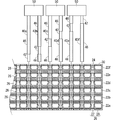
- FIG. 1 is a plan view showing a circuit device according to the first embodiment.
- FIG. 2 is a schematic cross-sectional view taken along the line II-II in FIG.
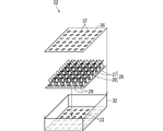
- FIG. 3 is an exploded perspective view showing one layer in the laminated body.
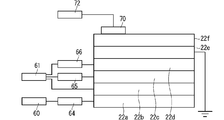
- FIG. 4 is a block diagram showing a connection example when the circuit device is applied to a vehicle.
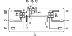
- FIG. 5 is a block diagram showing a wiring example when the circuit device is applied to a vehicle.
- FIG. 6 is a side view showing the circuit device according to the second embodiment.
- FIG. 7 is a side view showing the circuit device according to the third embodiment.
- FIG. 8 is an exploded perspective view showing the circuit device according to the fourth embodiment.
- FIG. 9 is an exploded perspective view showing a modified example of the laminated body.
- FIG. 10 is an exploded perspective view showing another modified example of the laminated body.
- the circuit device of the present disclosure is as follows. (1) A laminated body and a plurality of terminals are provided, the laminated body includes a plurality of layers, and the laminated body is formed with a plurality of holes penetrating the plurality of layers, and the plurality of layers are each formed.
- the connecting member has a connecting member formed of a conductor, and the connecting member has a plurality of connecting portions provided at positions corresponding to the plurality of holes, and a connecting portion for connecting the plurality of connecting portions.
- the plurality of terminals include a plurality of types of terminals corresponding to the plurality of layers, and the plurality of types of terminals are each inserted into any hole among the plurality of the holes and among the plurality of layers.
- a circuit device that can be selectively connected to the connection portion of any one of the corresponding layers.
- a plurality of terminals a plurality of types of terminals corresponding to a plurality of layers are provided, and each of the plurality of types of terminals is inserted into any one of a plurality of insertion ports and any one of the plurality of layers.
- the plurality of types of terminals include a coated terminal, the coated terminal has a terminal body and an insulating coating, and the terminal body has a first portion corresponding to a layer to be connected. It is also conceivable that the insulating coating is formed around the second portion, having a second portion corresponding to a layer that is not a connection partner. In this case, the insulation coating can prevent the terminal body from being connected to a layer that is not a connection partner.
- the plurality of layers have a first layer and a second layer
- the plurality of types of terminals include a terminal for the first layer and a terminal for the second layer
- the second layer is the first layer.
- the terminal is located on the side where the terminal is inserted from the layer
- the terminal for the first layer is a terminal connected to the first layer
- the terminal for the second layer is a terminal connected to the second layer. Yes, it may be shorter than the first layer terminal. In this case, since the second layer terminal is shorter than the first layer terminal, it is difficult to connect to the first layer.
- the hole formed in the first layer is smaller than the hole formed in the second layer, and the terminal for the first layer is the hole formed in the first layer and the second.
- the terminal for the second layer is connected to the second layer while penetrating the hole formed in the second layer.
- the holes are formed larger than the holes formed in the first layer.
- the second layer terminal since it is difficult for the second layer terminal to penetrate the hole formed in the first layer, it is difficult for the second layer terminal to be connected to the first layer.
- the thickness of each layer in the plurality of layers is different. In this case, since the intervals between the terminals connected to the layers are different, it is possible to prevent the terminals from being used in a state of insufficient insertion.
- the plurality of layers include a plurality of voltage layers having different voltage values in the connecting member.
- the terminals can be selectively connected to different power supply voltages.
- the plurality of voltage layers are stacked so that the voltage values increase in order from the side where the terminals are inserted. In this case, it is easy to prevent the terminals for the low voltage layer from being erroneously connected to the high voltage layer.
- the plurality of voltage layers are a first voltage layer connected to a first battery having a first voltage value and a second voltage layer having a second voltage value lower than the first voltage value. It may also include a second voltage layer connected to the battery. In this case, different power supply voltages can be easily supplied.
- the plurality of layers may include a communication layer.
- a communication line can be connected to the communication layer.
- the electronic control unit is further provided, and the electronic control unit is connected to the communication layer, and among the signals sent from the external device, the signal to the device connected to the communication layer is selectively selected. It is also possible to send it to the communication layer. In this case, it is possible to select whether the signal is for the device connected to the communication layer.
- FIG. 1 is a plan view showing a circuit device 10 according to the first embodiment.
- FIG. 2 is a schematic cross-sectional view taken along the line II-II in FIG. Note that the terminal 40 is not shown as a cross-sectional view in FIG.
- FIG. 3 is an exploded perspective view showing one layer 22 in the laminated body 20.
- the circuit device 10 includes a laminate 20 and a plurality of terminals 40.
- the laminate 20 includes a plurality of (six in this case) layers 22.
- a plurality of holes 24 penetrating the plurality of layers 22 are formed in the laminated body 20.
- a terminal 40 can be inserted into each hole 24.
- the opening of the hole 24 in the laminated body 20 is used as an insertion port for inserting the terminal 40.
- the terminal 40 inserted into the hole 24 is electrically connected to any one of the plurality of layers 22.
- the different layers 22 in the laminated body 20 are not electrically connected to each other.
- each layer 22 has a common structure. However, each layer may have a different structure. In the following, when it is necessary to distinguish between the six layers 22, they may be referred to as layers 22a, 22b, 22c, 22d, 22e, 22f.
- Each layer 22 has a connecting member 26 formed of a conductor.
- the connecting member 26 has a plurality of connecting portions 27 and a connecting portion 28 that connects the plurality of connecting portions 27 to each other.
- the plurality of connecting portions 27 are provided at positions corresponding to each of the plurality of holes 24. Since the plurality of connecting portions 27 are connected by the connecting portion 28 in one layer 22, the plurality of connecting portions 27 have the same potential.
- a plurality of holes 29 are formed in the flat plate-shaped member to form a connecting portion 28.
- the connecting portion 27 has a pair of plate-shaped portions formed so as to project from the peripheral edge portion of the hole 29 in the axial direction of the hole 29.
- the plate-shaped portion is formed like a leaf spring.
- the portion of the pair of plate-shaped portions from the base end portion to the intermediate portion is formed so as to gradually approach and close the hole 29.
- the portions of the pair of plate-shaped portions from the intermediate portion to the tip portion are formed so as to gradually separate and open holes 29.
- the distance between the closest contact portions where the pair of plate-shaped portions are closest to each other is smaller than the thickness dimension of the terminal 40.
- the tip portion rather than the closest contact portion is regarded as an induction portion that invites the terminal 40 to the closest contact portion. Therefore, when the terminal 40 is inserted into the hole 24, the tip of the terminal 40 is guided from the guide portion to the closest contact portion, and the closest contact portion expands and contacts the terminal 40.
- connection portion 27 can be electrically connected to the terminal 40.
- the connecting portion 27 and the connecting portion 28 may be separately molded and welded.
- the connecting portion 27 may be formed by cutting up a part of the flat plate-shaped member constituting the connecting portion 28.
- each layer 22 has a housing 30.
- the housing 30 can accommodate the connecting member 26.
- the connecting member 26 housed in the housing 30 is supported at a fixed position in the housing 30.
- the housings 30 are positioned and overlapped with each other, so that the connecting member 26 of each layer 22 is supported at a fixed position in the laminated body 20. Therefore, the housing 30 functions as a support member that supports the connecting member 26 at a fixed position.
- the housing 30 has a box 32 and a lid 36.
- the box 32 is formed in the shape of a rectangular parallelepiped box with one side open. It is possible to accommodate the connecting member 26 inside the box 32.
- the lid 36 is formed in the shape of a square flat plate. With the connecting member 26 housed inside the box 32, the lid 36 can close the opening of the box 32. Here, the surface of the box 32 facing the stacking direction is open. Therefore, a plurality of holes 33 are formed in the bottom plate of the box 32 located on the opposite side of the opening. Further, a plurality of holes 37 are also formed in the lid 36. The holes 33 in the bottom plate of the box 32 and the holes 37 in the lid 36 are formed at positions corresponding to the holes 29 in the connecting member 26.
- the holes 33 in the bottom plate of the box 32 and the holes 37 in the lid 36 have the same arrangement, and form a part of the holes 24 in the laminated body 20 together with the holes 29 in the connecting member 26. Further, the arrangement of the holes 33 and 37 is the same among the plurality of housings 30.
- the lid 36 in the housing 30 other than the housing 30 located at one end in the stacking direction may be omitted.
- the housing 30 that overlaps the opening side with respect to the housing 30 in which the lid 36 is omitted can be a lid that closes the opening of the housing 30 in which the lid 36 is omitted.
- a fixing portion for fixing the laminated housings 30 is provided.
- a screw hole may be formed as a fixing portion in a corner of the box 32, and a plurality of housings 30 may be screwed.
- a convex portion and a concave portion for uniting the boxes 32 may be formed.
- the plurality of terminals 40 include a plurality of types of terminals 40a, 40b, 40c, 40d, 40e, and 40f corresponding to the plurality of layers 22, respectively.
- the plurality of types of terminals 40a, 40b, 40c, 40d, 40e, 40f are each inserted into any hole 24 of the plurality of holes 24, and any one of the plurality of layers 22 corresponding layers 22a, 22b, It can be selectively connected to the connection portion 27 of 22c, 22d, 22e, and 22f.
- the terminal 40a is connected to the layer 22a
- the terminal 40b is connected to the layer 22b
- the terminal 40c is connected to the layer 22c
- the terminal 40d is connected to the layer 22d
- the terminal 40e is connected to the layer 22e
- the terminal 40f is connected. It will be described as being connected to the layer 22f.
- a plurality of types of terminals 40a, 40b, 40c, 40d, 40e, and 40f are coated terminals.
- the coated terminal has a terminal body 42 and an insulating coating 46.
- the terminal body 42 is formed of a conductor.
- the terminal body 42 has a first portion corresponding to the layer 22 which is a connection partner and a second portion corresponding to a layer 22 which is not a connection partner.
- An insulating coating 46 is formed around the second portion.
- the terminal body 42 is formed in a common shape in the plurality of types of terminals 40a, 40b, 40c, 40d, 40e, and 40f.
- the plurality of types of terminals 40a, 40b, 40c, 40d, 40e, and 40f can be connected to the predetermined layer 22 by being inserted into the laminate 20. Further, the plurality of types of terminals 40a, 40b, 40c, 40d, 40e, and 40f can be removed from the laminated body 20 to eliminate the connection state with the predetermined layer 22. Therefore, by attaching and detaching the plurality of types of terminals 40a, 40b, 40c, 40d, 40e, and 40f to the laminated body 20, it becomes possible to cope with the design change in the circuit device 10.
- the plurality of terminals 40 are held by the holding member 50.
- the plurality of terminals 40 are grouped into equipment units, system units, and the like, and are held by different holding members 50 for each group.
- the plurality of terminals 40 held by the holding member 50 can be collectively attached to and detached from the laminated body 20.
- the terminal 40 protrudes from the holding member 50 by a predetermined length.
- the holding member 50 may be in contact with the surface of the laminated body 20 in a state where the terminals 40 are inserted into the laminated body 20 by a predetermined length. In this case, the holding member 50 suppresses the insertion amount of the terminal 40 from the laminated body 20 from becoming excessive.
- the holding member 50 may be a part of the device, or may be a connector housing provided at the end of an electric wire extending from the device.
- FIG. 4 is a block diagram showing a connection example when the circuit device 10 is applied to a vehicle.
- the vehicle to which the circuit device 10 is applied is a vehicle having a plurality of batteries 60 and 61, such as a hybrid vehicle and an electric vehicle, will be described.
- layers 22a, 22b, 22c, and 22d are voltage layers
- layer 22e is a ground layer
- layer 22f is a communication layer.
- the plurality of layers 22 include the plurality of voltage layers 22a, 22b, 22c, 22d, the ground layer 22e, and the communication layer 22f.
- the terminal 40 is inserted into the circuit device 10 from the communication layer 22f side.
- the communication layer 22f, the ground layer 22e, and the plurality of voltage layers 22d, 22c, 22b, and 22a are laminated in this order from the insertion port side of the terminal 40.
- the plurality of voltage layers 22a, 22b, 22c, and 22d are stacked so that the voltage values increase in order from the insertion port side of the terminal 40 (the side of the communication layer 22f in the example shown in FIG. 4). Therefore, here, the voltage values are higher in the order of the voltage layer 22d, the voltage layer 22c, the voltage layer 22b, and the voltage layer 22a.
- the voltage values in the plurality of voltage layers 22d, 22c, 22b, and 22a are 3.3 volts, 5 volts, 12 volts, and 24 volts, respectively.
- the plurality of layers 22 include a plurality of voltage layers having different voltage values in the connecting member 26.
- the 3.3 volt and 5 volt voltage layers may be used as a power source for communication
- the 12 volt and 24 volt voltage layers may be used as a power source other than for communication.
- the plurality of voltage layers include a first voltage layer and a second voltage layer.
- the first voltage layer is a voltage layer connected to the first battery 60 having the first voltage value.
- the second voltage layer is connected to a second battery 61 having a second voltage value lower than the first voltage value.
- the first battery 60 is a drive battery
- the second battery 61 is an auxiliary battery.
- the first voltage value in the first battery 60 is, for example, several hundred volts.
- the second voltage value in the second battery 61 is, for example, 12 volts.
- the voltage layer 22a is connected to the drive battery 60, and the voltage layers 22b, 22c, 22d are connected to the auxiliary battery 61. Therefore, here, the voltage layer 22a is the first voltage layer, and the voltage layers 22b, 22c, and 22d are the second voltage layers. It is conceivable that the voltage layer 22a is connected to the drive battery 60 via a transformer (DC-DC converter) 64. As a result, the voltage value of the drive battery 60 can be converted into a predetermined voltage value in the voltage layer 22a.
- DC-DC converter transformer
- the voltage layers 22c and 22d set to voltage values different from the voltage value of the auxiliary battery 61 are also connected to the auxiliary battery 61 via the DC-DC converters 65 and 66, respectively.
- the voltage value of the auxiliary battery 61 can be converted into a predetermined voltage value in the respective voltage layers 22c and 22d.
- each voltage layer 22a, 22b, 22c, 22d may have a separate battery connection port to which a terminal provided at an end of an electric wire for supplying power from the batteries 60, 61 is connected.
- An electronic control unit (ECU: Electronic Control Unit) 70 is connected to the communication layer 22f.
- the circuit device 10 further includes the ECU 70.
- the ECU 70 selectively sends a signal to the device connected to the communication layer 22f among the signals sent from the external device to the communication layer 22f. This makes it difficult for the device connected to the communication layer 22f to receive unnecessary signals.
- the terminal 40 in the ECU 70 is inserted into the insertion port of the terminal 40 in the laminated body 20 and connected to the communication layer 22f.
- the communication layer 22f may have a separate ECU connection port for connecting to the terminal in the ECU 70.
- the ground layer 22e is connected to the minus side wiring of the device connected to each of the voltage layers 22a, 22b, 22c, 22d in the circuit device 10.
- the circuit device 10 is provided with only one ground layer 22e.
- the ground layer 22e is connected to, for example, the vehicle body ground.
- the terminal at the end of the wiring used for connecting the ground layer 22e and the vehicle body ground is connected to a ground terminal connection port provided separately from the insertion port of the terminal 40 in the laminated body 20.
- the terminal at the end of the wiring used for connecting the ground layer 22e and the vehicle body ground may be inserted into the insertion port of the terminal 40 in the laminated body 20 and connected to the ground layer 22e.
- the ground layer 22e may be connected to the negative side of the battery via an electric wire.
- FIG. 5 is a block diagram showing a wiring example when the circuit device 10 is applied to the vehicle 90.
- a plurality of (three in this case) circuit devices 10 are mounted on the vehicle 90.
- circuit devices 10a, 10b, and 10c When it is necessary to distinguish between the three circuit devices, they are referred to as circuit devices 10a, 10b, and 10c.
- the plurality of circuit devices 10 are connected to the drive battery 60 and the auxiliary battery 61, respectively.
- power is supplied to the voltage layers 22a, 22b, 22c, and 22d in each circuit device 10.
- the ECU 70s in the plurality of circuit devices 10 are each connected to the central ECU 72.
- a plurality of devices 80 are connected to each of the plurality of circuit devices 10 in the vehicle.
- a plurality of devices 80 are connected to a circuit device 10 located near the device 80. Further, for example, it is conceivable that the plurality of devices 80 are connected to the circuit device 10 located in the same space as itself (for example, in the engine room, in the instrument panel, door, vehicle room, trunk room, etc.).
- the devices 80a, 80b, 80c (for example, headlamps, sensors, etc.) mounted on the front portion of the vehicle 90 are connected to the circuit device 10a mounted on the front portion of the vehicle 90. ..
- the devices 80d, 80e, 80f (for example, door lock, power window, side mirror, etc.) mounted on the door are connected to the circuit device 10b mounted on the door.
- the devices 80g, 80h, 80i (for example, tail lamps, sensors, etc.) mounted on the rear portion of the vehicle 90 are connected to the circuit device 10c mounted on the rear portion of the vehicle 90.
- a plurality of types of terminals 40a, 40b, 40c, 40d, 40e, and 40f corresponding to the plurality of layers 22 are provided as the plurality of terminals 40, and a plurality of types of terminals are provided.
- the terminals 40a, 40b, 40c, 40d, 40e, and 40f are each inserted into any of the plurality of insertion ports and selectively with the connection portion 27 of the corresponding layer 22 of any one of the plurality of layers 22. Since it is possible to connect to a predetermined layer 22 by inserting and removing the terminal 40, it is possible to easily respond to a design change at the connection portion of the circuit. Since the coated terminal having the terminal body 42 and the insulating coating 46 is adopted, it is possible to prevent the terminal main body 42 from being connected to the layer 22 which is not a connection partner by the insulating coating 46.
- the terminals 40 can be selectively connected to different power supply voltages. Since the plurality of voltage layers 22a, 22b, 22c, and 22d are laminated so that the voltage values increase in order from the side where the terminals 40 are inserted, the terminals 40d for the low voltage layer 22d are erroneously placed on the high voltage layer 22a. It is easy to suppress the connection.
- the plurality of voltage layers 22a, 22b, 22c, and 22d have a first voltage layer 22a connected to a first battery 60 having a first voltage value, and a second voltage value lower than the first voltage value. Since the second voltage layers 22b, 22c, and 22d connected to the second battery 61 are included, different power supply voltages can be easily supplied.
- a communication line can be connected to the communication layer 22f.
- the electronic control unit 70 is connected to the communication layer 22f, and among the signals sent from the external device, the signal to the device 80 connected to the communication layer 22f is selectively sent to the communication layer 22f, so that the communication layer 22f It is possible to select whether it is a signal for the device 80 connected to the device 80.
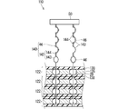
- FIG. 6 is a side view showing the circuit device 110 according to the second embodiment.
- the same reference numerals will be given to the components as described above, and the description thereof will be omitted. The same applies to the following description of each embodiment.
- the connecting member 26 is formed in a leaf spring shape, but in this example, the terminal 140 is formed in a leaf spring shape. More specifically, in this example, a plurality of holes 29 are formed in the conductor plate to form the connecting member 126.
- a plurality of connecting members 126 are insulated from each other by an insulating portion 138.
- an insulating plate is arranged between a plurality of connecting members 126, or an insulating film is formed on the surface of the connecting member 126 to form an insulating portion 138.
- the insulating portion 138 is provided so as not to block the hole 29 in the connecting member 126. In other words, a hole corresponding to the hole 29 is also formed in the insulating portion 138.
- the terminal 140 includes a terminal body 142 and an insulating coating 46.
- the terminal body 142 has a plurality of contact portions 143 and a connecting plate portion 144.
- the contact portion 143 is a portion that is inserted into the hole 29 of the connecting member 126 and is electrically connected to the connecting member 126.
- the contact portion 143 is formed in a leaf spring shape.
- the plurality of contact portions 143 are arranged in one direction.
- the connecting plate portion 144 connects a plurality of contact portions 143 to each other.
- the terminal body 142 is formed by bending a conductor plate.
- the insulating coating 46 is formed on a portion of the terminal body 142 excluding the contact portion 43 corresponding to the layer 122 to be connected.
- FIG. 7 is a side view showing the circuit device 210 according to the third embodiment.
- each layer 222 in the plurality of layers 222 is different.
- the terminal 240 is formed in a leaf spring shape will be described as in the example shown in FIG.
- the connecting member 26 may be formed in a leaf spring shape.
- the thickness of the connecting member 126 is the same.
- the thickness of each layer 222 in the plurality of layers 222 is different due to the difference in the thickness of the insulating portion 238.
- the thickness of each layer 222 in the plurality of layers 222 may be different due to the difference in the thickness of the connecting member 126.
- the distance between the contact portions 243 in the terminal body 242 is different.
- the lengths of the connecting plate portions 244 connecting the contact portions 243 are different.
- the plurality of layers 222 are arranged in ascending order of thickness, but this is not an essential configuration.
- the order of the plurality of layers can be set as appropriate.
- FIG. 8 is an exploded perspective view showing the circuit device 310 according to the fourth embodiment.
- the plurality of layers in the circuit device 310 include a first layer 322a and a second layer 322b.
- the second layer 322b is a layer located on the side where the terminal is inserted from the first layer 322a.
- the holes 324a formed in the first layer 322a are smaller than the holes 324b formed in the second layer 322b.
- the plurality of types of terminals in the circuit device 310 include a first layer terminal 340a and a second layer terminal 340b.
- the first layer terminal 340a is a terminal connected to the first layer 322a.
- the terminal for the first layer 340a is connected to the first layer 322a while penetrating the hole 324b formed in the second layer 322b and the hole 324a formed in the first layer 322a.
- the second layer terminal 340b is a terminal connected to the second layer 322b.
- the second layer terminal 340b is connected to the second layer 322b while penetrating the hole 324b formed in the second layer 322b.
- the second layer terminal 340b is shorter than the first layer terminal 340a. Further, the second layer terminal 340b is formed larger than the hole 324a formed in the first layer 322a.
- the second layer terminal 340b is shorter than the first layer terminal 340a in this way, it is difficult for the second layer terminal 340b to be connected to the first layer 322a. Further, if the terminal 340b for the second layer is larger than the hole 324a formed in the first layer 322a, it is difficult for the terminal 340b for the second layer to penetrate the hole 324a formed in the first layer 322a, so that it is used for the second layer. It is difficult for the terminal 340b to be connected to the first layer 322a.
- the holes 324a and 324b are formed in a T shape when viewed from the axial direction.
- the shapes of the terminals 340a and 340b are also formed in a T shape when viewed from the axial direction.
- the shapes of the holes 324a and 324b and the terminals 340a and 340b seen from the axial direction do not have to be T-shaped, and may be, for example, square or circular.
- the first layer terminal 340a is formed so that the size corresponding to the hole 324a formed in the first layer 322a is continuous in the axial direction, but this is not an essential configuration.
- one connecting member 26 is housed in one housing 30, this is not essential.
- a plurality of connecting members 26 may be housed in one housing 430 in a laminated state.
- the laminate may have only one housing 430 or may have a plurality of housings.
- the plurality of housings may include housings having a different number of connecting members 26 to be accommodated.
- a surface facing a direction orthogonal to the stacking direction of the connecting members 26 may be open.
- holes 33 and 37 are formed in the pair of side walls, respectively.
- the side wall in the box 432 is a surface orthogonal to the bottom plate located opposite to the opening.
- an edge supporting portion 34 capable of supporting the edge portion of the connecting portion 28 in the connecting member 26 may be formed in the box 432.
- the edge support portion 34 is formed on the side wall where the holes 33 and 37 are not formed, for example, in the box 432.
- the edge support portion 34 is formed in a groove shape extending from the opening side toward the bottom plate side on the side wall.
- a partition may be provided instead of the edge support portion 34.
- the partition is formed in a plate shape parallel to, for example, the side wall in which the holes 33 and 37 are formed, and divides the internal space of one box 432 in the stacking direction.
- the connecting member 26 is housed in each space partitioned by the partition. Holes corresponding to the holes 33 and 37 are formed in the partition.
- the laminated body 20 is configured to include six layers 22, but this is not an essential configuration.
- the laminate 20 may be configured to include two layers, three layers, four layers or five layers, or may be configured to include seven or more layers.
- the laminated body 20 includes the voltage layers 22a, 22b, 22c, 22d, the communication layer 22f, and the ground layer 22e, but this is not an essential configuration.
- the voltage layers 22a, 22b, 22c, 22d, the communication layer 22f, and the ground layer 22e the voltage layers 22a, 22b, 22c, 22d may be omitted, or the communication layer 22f may be omitted. It is possible, and the ground layer 22e may be omitted.
- the voltage layers 22a, 22b, 22c, 22d, the communication layer 22f, and the ground layer 22e two of the communication layer 22f and the ground layer 22e may be omitted.
- the laminate 20 may include at least one voltage layer.
- the circuit device 10 has been described as being applied to the vehicle 90 having a plurality of batteries 60 and 61 in the first embodiment, this is not essential.
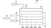
- the circuit device 510 may be applied to an automobile having only one battery 62 (for example, an engine automobile).
- the plurality of layers 522 include the plurality of voltage layers 522a and 522b
- at least one of the plurality of voltage layers 522a and 522b is connected to the one battery 62 via the DC-DC converters 67 and 68. It is good to have it.
- the voltage layers 522a and 522b are connected to the alternator.
- ground layer 22e there is one ground layer 22e, this is not an essential configuration.
- a ground layer may be provided separately for each voltage layer.
- ground layers 522c, 522d, and 522e may be provided at positions sandwiching the plurality of voltage layers 522a and 522b, respectively.
- connection member 26 has been described as a conductor plate in the first embodiment, this is not an essential configuration.
- the connecting member may be a conductor film or the like.
- the connecting member such as a conductor film may be formed on the surface of the substrate having an insulating property.
- a conductor film is formed on the entire surface of the substrate on which a plurality of holes are formed.
- a connecting portion is formed on the peripheral edge of the hole on the surface of the substrate on which a plurality of holes are formed, and a connecting portion is formed so as to connect the peripheral edges of the hole.
- connection example in which the circuit device 10 is applied to the vehicle shown in the first embodiment can also be regarded as a wiring system in the vehicle.
Landscapes
- Engineering & Computer Science (AREA)
- Microelectronics & Electronic Packaging (AREA)
- Manufacturing & Machinery (AREA)
- Metallurgy (AREA)
- Connector Housings Or Holding Contact Members (AREA)
- Coupling Device And Connection With Printed Circuit (AREA)
Abstract
回路の接続部分において設計変更に容易に対応できるようにする技術を提供することを目的とする。回路装置は、積層体と複数の端子とを備え、前記積層体は複数の層を含み、前記積層体には、前記複数の層を貫通する孔が複数形成されており、前記複数の層はそれぞれが、導体によって形成された接続部材を有し、前記接続部材は、複数の前記孔それぞれに対応する位置に設けられた複数の接続部と前記複数の接続部同士をつなぐ連結部とを有し、前記複数の端子は前記複数の層にそれぞれ対応する複数の種類の端子を含み、前記複数の種類の端子はそれぞれが複数の前記孔のうち任意の孔に挿入されて前記複数の層のうちいずれか1つの対応する層の前記接続部と選択的に接続可能である。
Description
本開示は、回路装置に関する。
特許文献1に記載された積層型ジョイントコネクタは、単層ハウジング内に複数本の積層端子を平面的に配列した単層ユニットを複数層積層して構成される積層体と、この積層体を積層方向に貫通して前記積層端子を選択的に接続する複数本の雄端子とを備えており、異なる層間の積層端子を雄端子によって接続している。
特許文献2に記載された電気接続箱は、モジュールプレート上に配した接続部材にそれぞれ電線を接続して該モジュールプレートを複数積層することによりモジュールプレートの積層体を構成し、該モジュールプレートの積層体に層間を貫き抜ける接続バーを貫通させて該接続バーにより各層間の接続部材同士を電気接続することにより、全体で所望の回路を構成している。
特許文献1に記載の積層型ジョイントコネクタにおいて回路構成に設計変更があった場合、電線の抜き差しが必要となり、端子の接続先を確認する必要がある。同様に特許文献2に記載の電気接続箱において回路構成に設計変更があった場合、電線接続金具の取り換えが必要となり、分解の必要がある。
そこで、回路の接続部分において設計変更に容易に対応できるようにする技術を提供することを目的とする。
本開示の回路装置は、積層体と複数の端子とを備え、前記積層体は複数の層を含み、前記積層体には、前記複数の層を貫通する孔が複数形成されており、前記複数の層はそれぞれが、導体によって形成された接続部材を有し、前記接続部材は、複数の前記孔それぞれに対応する位置に設けられた複数の接続部と前記複数の接続部同士をつなぐ連結部とを有し、前記複数の端子は前記複数の層にそれぞれ対応する複数の種類の端子を含み、前記複数の種類の端子はそれぞれが複数の前記孔のうち任意の孔に挿入されて前記複数の層のうちいずれか1つの対応する層の前記接続部と選択的に接続可能である、回路装置である。
本開示によれば、回路の接続部分において設計変更が容易となる。
[本開示の実施形態の説明]
最初に本開示の実施態様を列記して説明する。
本開示の回路装置は、次の通りである。
(1)積層体と複数の端子とを備え、前記積層体は複数の層を含み、前記積層体には、前記複数の層を貫通する孔が複数形成されており、前記複数の層はそれぞれが、導体によって形成された接続部材を有し、前記接続部材は、複数の前記孔それぞれに対応する位置に設けられた複数の接続部と前記複数の接続部同士をつなぐ連結部とを有し、前記複数の端子は前記複数の層にそれぞれ対応する複数の種類の端子を含み、前記複数の種類の端子はそれぞれが複数の前記孔のうち任意の孔に挿入されて前記複数の層のうちいずれか1つの対応する層の前記接続部と選択的に接続可能である、回路装置である。
複数の端子として複数の層にそれぞれ対応する複数の種類の端子が設けられ、複数の種類の端子はそれぞれが複数の挿入口のうち任意の挿入口に挿入されて複数の層のうちいずれか1つの対応する層の接続部と選択的に接続可能であるため、端子の抜き差しによって所定の層に接続できるようになり、もって、回路の接続部分において設計変更に容易に対応できる。
(2)前記複数の種類の端子は、被覆付端子を含み、前記被覆付端子は、端子本体と絶縁被覆とを有し、前記端子本体は、接続相手である層に対応する第1部分と、接続相手ではない層に対応する第2部分とを有し、前記絶縁被覆が前記第2部分の周囲に形成されていることも考えられる。この場合、端子本体が接続相手とならない層と接続されることを絶縁被覆によって抑制できる。
(3)前記複数の層は第1層と第2層とを有し、前記複数の種類の端子は第1層用端子と第2層用端子とを含み、前記第2層は前記第1層よりも前記端子が挿入される側に位置し、前記第1層用端子は前記第1層に接続される端子であり、前記第2層用端子は前記第2層に接続される端子であり、前記第1層用端子よりも短いことも考えられる。この場合、第2層用端子が第1層用端子よりも短いため、第1層に接続されにくい。
(4)前記第1層に形成された前記孔は、前記第2層に形成された前記孔よりも小さく、前記第1層用端子は前記第1層に形成された前記孔及び前記第2層に形成された前記孔を貫通しつつ前記第1層に接続され、前記第2層用端子は前記第2層に形成された前記孔を貫通しつつ前記第2層に接続されており、前記第1層に形成された前記孔よりも大きく形成されていることも考えられる。この場合、第2層用端子が第1層に形成された孔を貫通しにくいため、第2層用端子が第1層に接続されにくい。
(5)前記複数の層における各層の厚みが異なっていることも考えられる。この場合、端子においても層に接続される部分の間隔が異なるため、差込不足の状態で使用されることを抑制できる。
(6)前記複数の層は、前記接続部材における電圧値が相互に異なる複数の電圧層を含むことも考えられる。この場合、端子が異なる電源電圧に選択的に接続可能となる。
(7)前記複数の電圧層は、前記端子が挿入される側から順に前記電圧値が高くなるように積層されていることも考えられる。この場合、低圧の層用の端子が高圧の層に誤って接続されることを抑制しやすい。
(8)前記複数の電圧層は、第1の電圧値を有する第1のバッテリに接続された第1電圧層と、前記第1の電圧値よりも低い第2の電圧値を有する第2のバッテリに接続された第2電圧層とを含むことも考えられる。この場合、異なる電源電圧を簡易に供給可能となる。
(9)前記複数の層は通信層を含むことも考えられる。この場合、通信層に通信線を接続できる。
(10)電子制御ユニットをさらに備え、前記電子制御ユニットは前記通信層に接続されており、外部機器から送られてきた信号のうち前記通信層に接続された機器への信号を選択的に前記通信層に送ることも考えられる。この場合、通信層に接続された機器に対する信号かを取捨選択できる。
最初に本開示の実施態様を列記して説明する。
本開示の回路装置は、次の通りである。
(1)積層体と複数の端子とを備え、前記積層体は複数の層を含み、前記積層体には、前記複数の層を貫通する孔が複数形成されており、前記複数の層はそれぞれが、導体によって形成された接続部材を有し、前記接続部材は、複数の前記孔それぞれに対応する位置に設けられた複数の接続部と前記複数の接続部同士をつなぐ連結部とを有し、前記複数の端子は前記複数の層にそれぞれ対応する複数の種類の端子を含み、前記複数の種類の端子はそれぞれが複数の前記孔のうち任意の孔に挿入されて前記複数の層のうちいずれか1つの対応する層の前記接続部と選択的に接続可能である、回路装置である。
複数の端子として複数の層にそれぞれ対応する複数の種類の端子が設けられ、複数の種類の端子はそれぞれが複数の挿入口のうち任意の挿入口に挿入されて複数の層のうちいずれか1つの対応する層の接続部と選択的に接続可能であるため、端子の抜き差しによって所定の層に接続できるようになり、もって、回路の接続部分において設計変更に容易に対応できる。
(2)前記複数の種類の端子は、被覆付端子を含み、前記被覆付端子は、端子本体と絶縁被覆とを有し、前記端子本体は、接続相手である層に対応する第1部分と、接続相手ではない層に対応する第2部分とを有し、前記絶縁被覆が前記第2部分の周囲に形成されていることも考えられる。この場合、端子本体が接続相手とならない層と接続されることを絶縁被覆によって抑制できる。
(3)前記複数の層は第1層と第2層とを有し、前記複数の種類の端子は第1層用端子と第2層用端子とを含み、前記第2層は前記第1層よりも前記端子が挿入される側に位置し、前記第1層用端子は前記第1層に接続される端子であり、前記第2層用端子は前記第2層に接続される端子であり、前記第1層用端子よりも短いことも考えられる。この場合、第2層用端子が第1層用端子よりも短いため、第1層に接続されにくい。
(4)前記第1層に形成された前記孔は、前記第2層に形成された前記孔よりも小さく、前記第1層用端子は前記第1層に形成された前記孔及び前記第2層に形成された前記孔を貫通しつつ前記第1層に接続され、前記第2層用端子は前記第2層に形成された前記孔を貫通しつつ前記第2層に接続されており、前記第1層に形成された前記孔よりも大きく形成されていることも考えられる。この場合、第2層用端子が第1層に形成された孔を貫通しにくいため、第2層用端子が第1層に接続されにくい。
(5)前記複数の層における各層の厚みが異なっていることも考えられる。この場合、端子においても層に接続される部分の間隔が異なるため、差込不足の状態で使用されることを抑制できる。
(6)前記複数の層は、前記接続部材における電圧値が相互に異なる複数の電圧層を含むことも考えられる。この場合、端子が異なる電源電圧に選択的に接続可能となる。
(7)前記複数の電圧層は、前記端子が挿入される側から順に前記電圧値が高くなるように積層されていることも考えられる。この場合、低圧の層用の端子が高圧の層に誤って接続されることを抑制しやすい。
(8)前記複数の電圧層は、第1の電圧値を有する第1のバッテリに接続された第1電圧層と、前記第1の電圧値よりも低い第2の電圧値を有する第2のバッテリに接続された第2電圧層とを含むことも考えられる。この場合、異なる電源電圧を簡易に供給可能となる。
(9)前記複数の層は通信層を含むことも考えられる。この場合、通信層に通信線を接続できる。
(10)電子制御ユニットをさらに備え、前記電子制御ユニットは前記通信層に接続されており、外部機器から送られてきた信号のうち前記通信層に接続された機器への信号を選択的に前記通信層に送ることも考えられる。この場合、通信層に接続された機器に対する信号かを取捨選択できる。
[本開示の実施形態の詳細]
本開示の回路装置の具体例を、以下に図面を参照しつつ説明する。なお、本発明はこれらの例示に限定されるものではなく、請求の範囲によって示され、請求の範囲と均等の意味および範囲内でのすべての変更が含まれることが意図される。
本開示の回路装置の具体例を、以下に図面を参照しつつ説明する。なお、本発明はこれらの例示に限定されるものではなく、請求の範囲によって示され、請求の範囲と均等の意味および範囲内でのすべての変更が含まれることが意図される。
[実施形態1]
以下、実施形態1にかかる回路装置について説明する。図1は実施形態1にかかる回路装置10を示す平面図である。図2は図1におけるII-II線に沿った概略断面図である。なお図2において端子40は断面図とされていない。図3は積層体20における一の層22を示す分解斜視図である。
以下、実施形態1にかかる回路装置について説明する。図1は実施形態1にかかる回路装置10を示す平面図である。図2は図1におけるII-II線に沿った概略断面図である。なお図2において端子40は断面図とされていない。図3は積層体20における一の層22を示す分解斜視図である。
回路装置10は、積層体20と複数の端子40とを備える。積層体20は、複数(ここでは6つ)の層22を含む。積層体20には、複数の層22を貫通する孔24が複数形成されている。各孔24には端子40が挿入可能である。積層体20における孔24の開口部が端子40を挿入する挿入口とされる。孔24に挿入された端子40は、複数の層22のいずれかと電気的に接続される。積層体20において異なる層22同士は電気的に接続されていない。ここでは各層22は、共通の構成を有している。もっとも各層は異なる構成を有していてもよい。以下では、6つの層22について区別する必要がある場合、層22a、22b、22c、22d、22e、22fと称することがある。
各層22は、導体によって形成された接続部材26を有する。接続部材26は、複数の接続部27と複数の接続部27同士をつなぐ連結部28とを有する。複数の接続部27は、複数の孔24それぞれに対応する位置に設けられている。一の層22において複数の接続部27は連結部28によってつながっているため、複数の接続部27は同電位とされる。本例では平板状部材に複数の孔29が形成されて連結部28とされている。接続部27は、孔29の周縁部から孔29の軸方向に突出するように形成された一対の板状部を有している。板状部は板バネ状に形成されている。より詳細には、一対の板状部における基端部から中間部までの部分は、徐々に接近して孔29を塞ぐように形成されている。一対の板状部における中間部から先端部までの部分は、徐々に離間して孔29を開くように形成されている。一対の板状部が最も接近した最近接部の間隔は、端子40の厚み寸法よりも小さくなっている。最近接部よりも先端部が最近接部に端子40を誘い込む誘導部とされている。従って、端子40が孔24に挿入されると、端子40の先端が誘導部から最近接部に導かれ、最近接部が広がりつつ端子40に接触する。これにより接続部27のうち少なくとも最近接部が端子40と電気的に接続可能とされている。接続部27と連結部28とは別に成形されて溶接されていてもよい。連結部28を構成する平板状部材の一部が切り起こされることによって接続部27が形成されていてもよい。
各層22の接続部材26は一定位置に支持されている。一定位置は、接続部材26における孔29の位置が合った位置である。ここでは、各層22がハウジング30を有している。ハウジング30は、接続部材26を収容可能である。ハウジング30に収容された接続部材26はハウジング30内の一定位置に支持される。そしてハウジング30同士が位置決めされつつ重なることによって積層体20において各層22の接続部材26が一定位置に支持される。従って、ハウジング30は接続部材26を一定位置に支持する支持部材として機能する。
ハウジング30は箱32と蓋36とを有する。箱32は一方が開口した直方体箱状に形成されている。箱32の内部に接続部材26を収容することが可能である。蓋36は方形平板状に形成されている。箱32の内部に接続部材26が収容された状態で、蓋36が箱32の開口部を塞ぐことが可能である。ここでは箱32のうち積層方向を向く面が開口している。このため箱32のうち開口部と反対側に位置する底板には複数の孔33が形成されている。また蓋36にも複数の孔37が形成されている。箱32の底板における孔33、及び蓋36における孔37は接続部材26における孔29に対応する位置に形成されている。つまり箱32の底板における孔33、及び蓋36における孔37は配列が同じであり、接続部材26における孔29と共に積層体20における孔24一部をなしている。また複数のハウジング30間で孔33、37の配列が同じである。
なお積層方向一端に位置するハウジング30以外のハウジング30における蓋36は省略されていてもよい。この場合、蓋36が省略されたハウジング30に対して開口部側に重なるハウジング30が、蓋36が省略されたハウジング30の開口部を塞ぐ蓋となることができる。
複数のハウジング30が積層される場合、積層されたハウジング30同士を固定する固定部が設けられていると良い。例えば箱32の隅などに固定部としてねじ穴が形成されて、複数のハウジング30がねじ止めされていてもよい。また例えば固定部として箱32同士を合体させる凸部と凹部とが形成されていてもよい。
複数の端子40は複数の層22にそれぞれ対応する複数の種類の端子40a、40b、40c、40d、40e、40fを含む。複数の種類の端子40a、40b、40c、40d、40e、40fはそれぞれが複数の孔24のうち任意の孔24に挿入されて複数の層22のうちいずれか1つの対応する層22a、22b、22c、22d、22e、22fの接続部27と選択的に接続可能である。ここでは端子40aが層22aに接続され、端子40bが層22bに接続され、端子40cが層22cに接続され、端子40dが層22dに接続され、端子40eが層22eに接続され、端子40fが層22fに接続されるものとして説明する。
複数の種類の端子40a、40b、40c、40d、40e、40fは、被覆付端子である。被覆付端子は、端子本体42と絶縁被覆46とを有する。端子本体42は、導体によって形成されている。端子本体42は、接続相手である層22に対応する第1部分と、接続相手ではない層22に対応する第2部分とを有する。絶縁被覆46が第2部分の周囲に形成されている。複数の種類の端子40a、40b、40c、40d、40e、40fにおいて端子本体42は共通の形状に形成されている。共通の形状である端子本体42に対して絶縁被覆46が設けられる位置が異なることによって、各層22に対応可能な複数の種類の端子40a、40b、40c、40d、40e、40fを得ることができる。
このように複数の種類の端子40a、40b、40c、40d、40e、40fは積層体20に差し込まれることによって、所定の層22に接続可能である。また複数の種類の端子40a、40b、40c、40d、40e、40fは積層体20から抜かれることによって、所定の層22との接続状態を解消可能である。このため、複数の種類の端子40a、40b、40c、40d、40e、40fが積層体20に対して脱着されることによって、回路装置10における設計変更に対応可能となる。
複数の端子40は保持部材50に保持されている。例えば複数の端子40は、機器単位、システム単位などにグループ分けされて、グループごとに別の保持部材50に保持されることが考えられる。これにより、保持部材50に保持された複数の端子40が積層体20に対して一括して着脱可能となる。端子40は保持部材50から所定の長さ分突出している。保持部材50は端子40が所定の長さ分だけ積層体20に差し込まれた状態で、積層体20における表面に接触するものであってもよい。この場合、保持部材50は、積層体20に対する端子40の差込量が過多となることを抑制する。保持部材50は、機器の一部であることも考えられるし、機器から延びる電線の端部に設けられたコネクタハウジングであることも考えられる。
<車両における回路装置>
上記回路装置10を車両に適用する例について説明する。図4は回路装置10を車両に適用する際の接続例を示すブロック図である。ここでは回路装置10が適用される車両が、ハイブリッド車、電気自動車などのように複数のバッテリ60、61を有する車両である事例を用いて説明する。
上記回路装置10を車両に適用する例について説明する。図4は回路装置10を車両に適用する際の接続例を示すブロック図である。ここでは回路装置10が適用される車両が、ハイブリッド車、電気自動車などのように複数のバッテリ60、61を有する車両である事例を用いて説明する。
回路装置10において、層22a、22b、22c、22dが電圧層であり、層22eがグランド層であり、層22fが通信層である。このように複数の層22は、複数の電圧層22a、22b、22c、22dとグランド層22eと通信層22fとを含んでいる。回路装置10に対して、通信層22f側から端子40が挿入される。回路装置10において、端子40の挿入口側から通信層22f、グランド層22e、複数の電圧層22d、22c、22b、22aの順に積層されている。
複数の電圧層22a、22b、22c、22dは、端子40の挿入口側(図4に示す例では通信層22fの側)から順に電圧値が高くなるように積層されている。従って、ここでは電圧層22d、電圧層22c、電圧層22b、電圧層22aの順に電圧値が高くなっている。例えば複数の電圧層22d、22c、22b、22aにおける電圧値は順に、3.3ボルト、5ボルト、12ボルト、24ボルトである。このように複数の層22は、接続部材26における電圧値が相互に異なる複数の電圧層を含んでいる。例えば、3.3ボルト及び5ボルトの電圧層は通信用電源として用いられ、12ボルト及び24ボルトの電圧層は通信用以外の電源として用いられることが考えられる。
複数の電圧層は、第1電圧層と第2電圧層とを含む。第1電圧層は第1の電圧値を有する第1のバッテリ60に接続された電圧層である。第2電圧層は、第1の電圧値よりも低い第2の電圧値を有する第2のバッテリ61に接続されている。例えば第1のバッテリ60は、駆動用バッテリであり、第2のバッテリ61は補機バッテリである。第1のバッテリ60における第1の電圧値は例えば数百ボルトである。第2のバッテリ61における第2の電圧値は例えば12ボルトである。
図4に示す例では、電圧層22aが駆動用バッテリ60に接続され、電圧層22b、22c、22dが補機バッテリ61に接続されている。従ってここでは、電圧層22aが第1電圧層であり、電圧層22b、22c、22dが第2電圧層である。電圧層22aについては変圧器(DC-DCコンバータ)64を介して駆動用バッテリ60と接続されることが考えられる。これにより、駆動用バッテリ60の電圧値を電圧層22aにおける所定の電圧値に変換することができる。また、補機バッテリ61の電圧値と異なる電圧値に設定されている電圧層22c、22dについてもそれぞれDC-DCコンバータ65、66を介して補機バッテリ61と接続されることが考えられる。これにより、補機バッテリ61の電圧値をそれぞれの電圧層22c、22dにおける所定の電圧値に変換することができる。
なお、バッテリ60、61から各電圧層22a、22b、22c、22dへの電源供給は積層体20における端子40の挿入口からされてもよい。つまりバッテリ60、61からの電源を供給する電線の端部に設けられた端子40が積層体20における孔24に差し込まれて、所定の電圧層22a、22b、22c、22dに接続されていてもよい。また各電圧層22a、22b、22c、22dは、バッテリ60、61からの電源を供給する電線の端部に設けられた端子が接続されるバッテリ接続口を別に有していてもよい。
通信層22fには電子制御ユニット(ECU:Electronic Control Unit)70が接続されている。このように回路装置10はECU70をさらに備えることが考えられる。ECU70は、外部機器から送られてきた信号のうち通信層22fに接続された機器への信号を選択的に通信層22fに送る。これにより通信層22fに接続された機器が不要な信号を受け取りにくくなる。図4に示す例では、ECU70における端子40は、積層体20における端子40の挿入口に差し込まれて通信層22fに接続されている。もっとも通信層22fは、ECU70における端子と接続するためのECU接続口を別に有していてもよい。
グランド層22eには回路装置10における各電圧層22a、22b、22c、22dに接続された機器のマイナス側の配線が接続される。ここでは回路装置10にグランド層22eが1つのみ設けられている。グランド層22eは例えば車体アースに接続される。グランド層22eと車体アースとの接続に用いられる配線の端部の端子は、積層体20における端子40の挿入口とは別に設けられたアース端子接続口に接続されている。もちろんグランド層22eと車体アースとの接続に用いられる配線の端部の端子は積層体20における端子40の挿入口に差し込まれてグランド層22eに接続されていてもよい。グランド層22eは、電線を介してバッテリのマイナス側に接続されてもよい。
図5は回路装置10を車両90に適用したときの配線例を示すブロック図である。図5に示す例では車両90に複数(ここでは3つ)の回路装置10が搭載されている。3つの回路装置について区別が必要な場合、回路装置10a、10b、10cと称する。複数の回路装置10はそれぞれ駆動用バッテリ60及び補機バッテリ61と接続されている。これにより各回路装置10における電圧層22a、22b、22c、22dに電源が供給される。また複数の回路装置10におけるECU70は、それぞれセントラルECU72に接続されている。そして車両において複数の回路装置10のそれぞれに対して複数の機器80が接続されている。例えば複数の機器80は、自身の近くに位置する回路装置10と接続されることが考えられる。また例えば複数の機器80は、自身と同じ空間(例えば、エンジンルーム、インストルメントパネル内、ドア、車室、トランクルームなど)に位置する回路装置10と接続されることが考えられる。
図5に示す例では、車両90の前部に搭載される機器80a、80b、80c(例えば、ヘッドランプ、センサ等)は、車両90の前部に搭載される回路装置10aに接続されている。またドアに搭載される機器80d、80e、80f(例えば、ドアロック、パワーウインドウ、サイドミラー等)は、ドアに搭載される回路装置10bに接続されている。車両90の後部に搭載される機器80g、80h、80i(例えば、テールランプ、センサ等)は、車両90の後部に搭載される回路装置10cに接続されている。
以上のように構成された回路装置10によると、複数の端子40として複数の層22にそれぞれ対応する複数の種類の端子40a、40b、40c、40d、40e、40fが設けられ、複数の種類の端子40a、40b、40c、40d、40e、40fはそれぞれが複数の挿入口のうち任意の挿入口に挿入されて複数の層22のうちいずれか1つの対応する層22の接続部27と選択的に接続可能であるため、端子40の抜き差しによって所定の層22に接続できるようになり、もって、回路の接続部分において設計変更に容易に対応できる。端子本体42と絶縁被覆46とを有する被覆付端子が採用されているため、端子本体42が接続相手とならない層22と接続されることを絶縁被覆46によって抑制できる。
複数の層22は、接続部材26における電圧値が相互に異なる複数の電圧層22a、22b、22c、22dを含むため、端子40が異なる電源電圧に選択的に接続可能となる。複数の電圧層22a、22b、22c、22dは、端子40が挿入される側から順に電圧値が高くなるように積層されているため、低圧の層22d用の端子40dが高圧の層22aに誤って接続されることを抑制しやすい。複数の電圧層22a、22b、22c、22dは、第1の電圧値を有する第1のバッテリ60に接続された第1電圧層22aと、第1の電圧値よりも低い第2の電圧値を有する第2のバッテリ61に接続された第2電圧層22b、22c、22dとを含むため、異なる電源電圧を簡易に供給可能となる。
また複数の層22は通信層22fを含むため、通信層22fに通信線を接続できる。電子制御ユニット70は通信層22fに接続されており、外部機器から送られてきた信号のうち通信層22fに接続された機器80への信号を選択的に通信層22fに送るため、通信層22fに接続された機器80に対する信号かを取捨選択できる。
[実施形態2]
実施形態2にかかる回路装置について説明する。図6は実施形態2にかかる回路装置110を示す側面図である。なお、本実施形態の説明において、これまで説明したものと同様構成要素については同一符号を付してその説明を省略する。以下の各実施形態の説明においても同様である。
実施形態2にかかる回路装置について説明する。図6は実施形態2にかかる回路装置110を示す側面図である。なお、本実施形態の説明において、これまで説明したものと同様構成要素については同一符号を付してその説明を省略する。以下の各実施形態の説明においても同様である。
実施形態1では接続部材26が板バネ状に形成されていたが、本例では端子140が板バネ状に形成されている。より詳細には、本例では、導体板に複数の孔29が形成されて接続部材126とされている。複数の接続部材126の間が絶縁部138によって絶縁されている。これにより隣り合う層122の接続部材126同士が接続されることが抑制される。例えば複数の接続部材126の間に絶縁板が配置されたり、接続部材126の表面に絶縁被膜が形成されたりして、絶縁部138が形成される。絶縁部138は接続部材126における孔29を塞がないように設けられる。換言すると、絶縁部138にも孔29に対応する孔が形成される。
端子140は端子本体142と絶縁被覆46とを備える。端子本体142は、複数の接点部143と連結板部144とを有する。接点部143は、接続部材126の孔29に差し込まれて、接続部材126と電気的に接続される部分である。接点部143は板バネ状に形成されている。複数の接点部143は一の方向に沿って並んでいる。連結板部144は複数の接点部143同士をつないでいる。例えば端子本体142は導体板が折り曲げられて形成される。絶縁被覆46は端子本体142のうち接続相手となる層122に対応する接点部43を除いた部分に形成される。
[実施形態3]
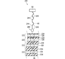
実施形態3にかかる回路装置について説明する。図7は実施形態3にかかる回路装置210を示す側面図である。
実施形態3にかかる回路装置について説明する。図7は実施形態3にかかる回路装置210を示す側面図である。
本例では、複数の層222における各層222の厚みが異なっている。ここでは、図6に示す例と同様に端子240が板バネ状に形成されている例で説明する。もちろん、図1に示す例と同様に、接続部材26が板バネ状に形成されていてもよい。
図7に示す例では接続部材126の厚みは同じである。図7に示す例では絶縁部238の厚みが異なることによって、複数の層222における各層222の厚みが異なっている。もちろん、接続部材126の厚みが異なることによって、複数の層222における各層222の厚みが異なっていてもよい。
複数の層222における各層222の厚みが異なっていることに対応するため、端子本体242において接点部243間の間隔が異なる。ここでは接点部243を結ぶ連結板部244の長さが異なる。これにより、積層体220における下の層222に接続される端子240が当該層222よりも上の層222まで差し込まれた状態において、つまり端子240が差込不足にある状態において端子240と積層体220とががたつきやすい。この結果、積層体220に対して端子240が差込不足の状態で使用されることを抑制できる。
図7に示す例では、複数の層222は厚みの薄い順に並んでいるが、このことは必須の構成ではない。複数の層の順番は適宜設定可能である。
[実施形態4]
実施形態4にかかる回路装置について説明する。図8は実施形態4にかかる回路装置310を示す分解斜視図である。
実施形態4にかかる回路装置について説明する。図8は実施形態4にかかる回路装置310を示す分解斜視図である。
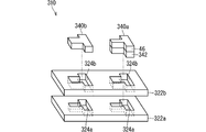
回路装置310における複数の層は第1層322aと第2層322bとを含む。第2層322bは第1層322aよりも端子が挿入される側に位置する層である。第1層322aに形成された孔324aは、第2層322bに形成された孔324bよりも小さい。
回路装置310における複数の種類の端子は第1層用端子340aと第2層用端子340bとを含む。第1層用端子340aは第1層322aに接続される端子である。第1層用端子340aは第2層322bに形成された孔324b及び第1層322aに形成された孔324aを貫通しつつ第1層322aに接続される。第1層用端子340aのうち第1層322aに接続されない部分、より具体的には第1層用端子340aが第1層322aに接続された状態で第2層322bにおける孔324bに収まる部分には、端子本体342の周囲に絶縁被覆46が形成されている。第2層用端子340bは第2層322bに接続される端子である。第2層用端子340bは第2層322bに形成された孔324bを貫通しつつ第2層322bに接続されている。第2層用端子340bは、第1層用端子340aよりも短い。また第2層用端子340bは、第1層322aに形成された孔324aよりも大きく形成されている。
このように第2層用端子340bが第1層用端子340aよりも短いと、第2層用端子340bが第1層322aに接続されにくい。また第2層用端子340bが第1層322aに形成された孔324aよりも大きいと、第2層用端子340bが第1層322aに形成された孔324aを貫通しにくいため、第2層用端子340bが第1層322aに接続されにくい。
本例では孔324a、324bの形状が軸方向から見てT字状に形成されている。これに合わせて端子340a、340bの形状も軸方向から見てT字状に形成されている。もちろん、軸方向から見た孔324a、324b及び端子340a、340bの形状はT字状である必要はなく、例えば方形状、円形状などであってもよい。第1層用端子340aは第1層322aに形成された孔324aに対応した大きさが軸方向に連続するように形成されているが、このことは必須の構成ではない。
[付記]
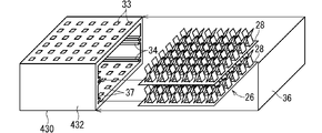
実施形態1において、一のハウジング30に一の接続部材26が収容されるものとして説明したが、このことは必須ではない。図9に示すように一のハウジング430に複数の接続部材26が積層状態で収容されていてもよい。この場合、積層体は一のハウジング430のみを有していてもよいし、複数のハウジングを有していてもよい。積層体が複数のハウジングを有する場合、複数のハウジングには、収容する接続部材26の数が異なるハウジングが含まれていてもよい。
実施形態1において、一のハウジング30に一の接続部材26が収容されるものとして説明したが、このことは必須ではない。図9に示すように一のハウジング430に複数の接続部材26が積層状態で収容されていてもよい。この場合、積層体は一のハウジング430のみを有していてもよいし、複数のハウジングを有していてもよい。積層体が複数のハウジングを有する場合、複数のハウジングには、収容する接続部材26の数が異なるハウジングが含まれていてもよい。
箱432において図9に示すように、接続部材26の積層方向と直交する方向を向く面が開口していてもよい。このような箱432において一対の側壁にそれぞれ孔33、37が形成される。ここで箱432における側壁とは、開口部と反対に位置する底板に直交する面である。またこのような箱432に複数の接続部材26を収容する場合、接続部材26における連結部28の縁部を支持可能な縁支持部34が箱432に形成されていてもよい。縁支持部34は、例えば箱432において孔33、37が形成されていない側壁に形成される。縁支持部34は側壁において開口部側から底板側に向けて延びる溝状に形成される。もっとも箱432において縁支持部34に代わって仕切りが設けられていてもよい。仕切りは、例えば孔33、37が形成された側壁と平行な板状に形成され、一の箱432の内部空間を積層方向に分割する。仕切りによって仕切られた各空間に接続部材26が収容される。仕切りには孔33、37に対応する孔が形成される。
実施形態1において積層体20が6つの層22を含むように構成されていたが、このことは必須の構成ではない。積層体20は2つの層、3つの層、4つの層又は5つの層を含むように構成されていてもよいし、7つ以上の層を含むように構成されていてもよい。また実施形態1において積層体20が電圧層22a、22b、22c、22dと通信層22fとグランド層22eとを含んでいたが、このことは必須の構成ではない。電圧層22a、22b、22c、22dと通信層22fとグランド層22eとのうち電圧層22a、22b、22c、22dが省略されている場合もあり得るし、通信層22fが省略されている場合もあり得るし、グランド層22eが省略されている場合もあり得る。電圧層22a、22b、22c、22dと通信層22fとグランド層22eとのうち通信層22fとグランド層22eとの2つが省略されている場合もあり得る。積層体20は少なくとも1つの電圧層を含んでいると良い。
実施形態1において回路装置10が複数のバッテリ60、61を備える車両90に適用されるものとして説明したが、このことは必須ではない。図10に示すように、バッテリ62が1つしかない自動車(例えばエンジン自動車)に回路装置510が適用されてもよい。この場合に、複数の層522が複数の電圧層522a、522bを含む場合、複数の電圧層522a、522bのうち少なくとも1つがDC-DCコンバータ67、68を介して当該1つのバッテリ62に接続されていると良い。なおエンジン自動車の場合、電圧層522a、522bはオルタネータに接続されていることも考えられる。
実施形態1においてグランド層22eが1つであるものとして説明したが、このことは必須の構成ではない。例えば、電圧層ごとにグランド層が別に設けられていてもよい。また例えば図10に示すように、複数の電圧層522a、522bをそれぞれ挟む位置にグランド層522c、522d、522eが設けられていてもよい。
実施形態1において接続部材26が導体板であるものとして説明したが、このことは必須の構成ではない。接続部材は導体膜などであってもよい。この場合、導体膜などである接続部材は、絶縁性を有する基板の表面に形成されているとよい。例えば、複数の孔が形成された基板の表面において全体に導体膜が形成されていることが感がられる。また例えば複数の孔が形成された基板の表面において孔の周縁に接続部が形成され、孔の周縁をつなぐように連結部が形成されていることも考えられる。
実施形態1において示した車両に回路装置10を適用した接続例は、車両における配線システムととらえることもできる。
なお、上記各実施形態及び各変形例で説明した各構成は、相互に矛盾しない限り適宜組み合わせることができる。
10、10a、10b、10c、110、210、310、510 回路装置
20、220、420 積層体
22、122、222、522 層
22a 第1電圧層(電圧層、層)
22b、22c、22d 第2電圧層(電圧層、層)
522a、522b 電圧層(層)
22e、522c、522d、522e グランド層(層)
22f 通信層(層)
322a 第1層(層)
322b 第2層(層)
24、324a、324b 孔
26、126 接続部材
27 接続部
28 連結部
29 孔
30 ハウジング
32 箱
33 孔
34 縁支持部
36 蓋
37 孔
138、238 絶縁部
40、140、240 端子
40a、40b、40c、40d、40e、40f 複数の種類の端子
340a 第1層用端子
340b 第2層用端子
42、142、242 端子本体
143、243 接点部
144、244 連結板部
46 絶縁被覆
50 保持部材
60 第1のバッテリ
61 第2のバッテリ
62 バッテリ
64、65、66、67、68 DC-DCコンバータ
70 電子制御ユニット(ECU)
72 セントラルECU
80、80a、80b、80c、80d、80e、80f、80g、80h、80i 機器
90 車両
20、220、420 積層体
22、122、222、522 層
22a 第1電圧層(電圧層、層)
22b、22c、22d 第2電圧層(電圧層、層)
522a、522b 電圧層(層)
22e、522c、522d、522e グランド層(層)
22f 通信層(層)
322a 第1層(層)
322b 第2層(層)
24、324a、324b 孔
26、126 接続部材
27 接続部
28 連結部
29 孔
30 ハウジング
32 箱
33 孔
34 縁支持部
36 蓋
37 孔
138、238 絶縁部
40、140、240 端子
40a、40b、40c、40d、40e、40f 複数の種類の端子
340a 第1層用端子
340b 第2層用端子
42、142、242 端子本体
143、243 接点部
144、244 連結板部
46 絶縁被覆
50 保持部材
60 第1のバッテリ
61 第2のバッテリ
62 バッテリ
64、65、66、67、68 DC-DCコンバータ
70 電子制御ユニット(ECU)
72 セントラルECU
80、80a、80b、80c、80d、80e、80f、80g、80h、80i 機器
90 車両
Claims (10)
- 積層体と複数の端子とを備え、
前記積層体は複数の層を含み、
前記積層体には、前記複数の層を貫通する孔が複数形成されており、
前記複数の層はそれぞれが、導体によって形成された接続部材を有し、
前記接続部材は、複数の前記孔それぞれに対応する位置に設けられた複数の接続部と前記複数の接続部同士をつなぐ連結部とを有し、
前記複数の端子は前記複数の層にそれぞれ対応する複数の種類の端子を含み、
前記複数の種類の端子はそれぞれが複数の前記孔のうち任意の孔に挿入されて前記複数の層のうちいずれか1つの対応する層の前記接続部と選択的に接続可能である、回路装置。 - 請求項1に記載の回路装置であって、
前記複数の種類の端子は、被覆付端子を含み、
前記被覆付端子は、端子本体と絶縁被覆とを有し、
前記端子本体は、接続相手である層に対応する第1部分と、接続相手ではない層に対応する第2部分とを有し、
前記絶縁被覆が前記第2部分の周囲に形成されている、回路装置。 - 請求項1又は請求項2に記載の回路装置であって、
前記複数の層は第1層と第2層とを有し、
前記複数の種類の端子は第1層用端子と第2層用端子とを含み、
前記第2層は前記第1層よりも前記端子が挿入される側に位置し、
前記第1層用端子は前記第1層に接続される端子であり、
前記第2層用端子は前記第2層に接続される端子であり、前記第1層用端子よりも短い、回路装置。 - 請求項3に記載の回路装置であって、
前記第1層に形成された前記孔は、前記第2層に形成された前記孔よりも小さく、
前記第1層用端子は前記第1層に形成された前記孔及び前記第2層に形成された前記孔を貫通しつつ前記第1層に接続され、
前記第2層用端子は前記第2層に形成された前記孔を貫通しつつ前記第2層に接続されており、前記第1層に形成された前記孔よりも大きく形成されている、回路装置。 - 請求項1から請求項4のいずれか1項に記載の回路装置であって、
前記複数の層における各層の厚みが異なっている、回路装置。 - 請求項1から請求項5のいずれか1項に記載の回路装置であって、
前記複数の層は、前記接続部材における電圧値が相互に異なる複数の電圧層を含む、回路装置。 - 請求項6に記載の回路装置であって、
前記複数の電圧層は、前記端子が挿入される側から順に前記電圧値が高くなるように積層されている、回路装置。 - 請求項6又は請求項7に記載の回路装置であって、
前記複数の電圧層は、第1の電圧値を有する第1のバッテリに接続された第1電圧層と、前記第1の電圧値よりも低い第2の電圧値を有する第2のバッテリに接続された第2電圧層とを含む、回路装置。 - 請求項1から請求項8のいずれか1項に記載の回路装置であって、
前記複数の層は通信層を含む、回路装置。 - 請求項9に記載の回路装置であって、
電子制御ユニットをさらに備え、
前記電子制御ユニットは前記通信層に接続されており、外部機器から送られてきた信号のうち前記通信層に接続された機器への信号を選択的に前記通信層に送る、回路装置。
Priority Applications (2)
| Application Number | Priority Date | Filing Date | Title |
|---|---|---|---|
| US17/438,074 US11894626B2 (en) | 2019-03-14 | 2019-12-19 | Circuit apparatus |
| CN201980093423.3A CN113519096B (zh) | 2019-03-14 | 2019-12-19 | 电路装置 |
Applications Claiming Priority (2)
| Application Number | Priority Date | Filing Date | Title |
|---|---|---|---|
| JP2019047232A JP7151567B2 (ja) | 2019-03-14 | 2019-03-14 | 回路装置及び電子制御ユニットと回路装置との接続構造 |
| JP2019-047232 | 2019-03-14 |
Publications (1)
| Publication Number | Publication Date |
|---|---|
| WO2020183850A1 true WO2020183850A1 (ja) | 2020-09-17 |
Family
ID=72427241
Family Applications (1)
| Application Number | Title | Priority Date | Filing Date |
|---|---|---|---|
| PCT/JP2019/049862 Ceased WO2020183850A1 (ja) | 2019-03-14 | 2019-12-19 | 回路装置 |
Country Status (4)
| Country | Link |
|---|---|
| US (1) | US11894626B2 (ja) |
| JP (1) | JP7151567B2 (ja) |
| CN (1) | CN113519096B (ja) |
| WO (1) | WO2020183850A1 (ja) |
Families Citing this family (4)
| Publication number | Priority date | Publication date | Assignee | Title |
|---|---|---|---|---|
| US10497635B2 (en) | 2018-03-27 | 2019-12-03 | Linear Technology Holding Llc | Stacked circuit package with molded base having laser drilled openings for upper package |
| US11844178B2 (en) * | 2020-06-02 | 2023-12-12 | Analog Devices International Unlimited Company | Electronic component |
| JP7740932B2 (ja) * | 2021-08-25 | 2025-09-17 | 古河電気工業株式会社 | コネクタおよび接続コネクタ構造体 |
| US11744021B2 (en) | 2022-01-21 | 2023-08-29 | Analog Devices, Inc. | Electronic assembly |
Citations (6)
| Publication number | Priority date | Publication date | Assignee | Title |
|---|---|---|---|---|
| JPS5177594U (ja) * | 1974-12-17 | 1976-06-18 | ||
| US4054939A (en) * | 1975-06-06 | 1977-10-18 | Elfab Corporation | Multi-layer backpanel including metal plate ground and voltage planes |
| JPH04134075U (ja) * | 1991-06-03 | 1992-12-14 | 株式会社アドバンテスト | プローブカード |
| JP2004030993A (ja) * | 2002-06-24 | 2004-01-29 | Furukawa Electric Co Ltd:The | 積層型ジョイントコネクタ |
| US7963776B1 (en) * | 2010-03-23 | 2011-06-21 | Tyco Electronics Corporation | Electrical connector assembly having direct connection terminals |
| JP2018116767A (ja) * | 2017-01-16 | 2018-07-26 | 株式会社オートネットワーク技術研究所 | 配線モジュール |
Family Cites Families (25)
| Publication number | Priority date | Publication date | Assignee | Title |
|---|---|---|---|---|
| US3022480A (en) * | 1957-02-07 | 1962-02-20 | Tiffany Frank Emery | Sandwich circuit strips |
| US3212049A (en) * | 1963-04-30 | 1965-10-12 | Ind Electronic Hardware Corp | Multilayer circuitry with placed bushings |
| US3400358A (en) * | 1965-10-21 | 1968-09-03 | Ibm | Electrical connector |
| US3853377A (en) * | 1971-12-27 | 1974-12-10 | B Shlesinger | Tight fitting plug connection and method for making same |
| US4446505A (en) * | 1982-03-22 | 1984-05-01 | Amp Incorporated | Electrical connector for interconnecting printed circuit boards |
| US4859188A (en) * | 1987-10-05 | 1989-08-22 | Cray Research, Inc. | Wire/disk board-to-board interconnect device |
| US4889496A (en) * | 1988-04-12 | 1989-12-26 | Intercon Systems, Inc. | Compressible core electrical connector |
| US5152696A (en) * | 1990-04-26 | 1992-10-06 | Cray Research, Inc. | Z-axis connectors for stacked printed circuit board assemblies |
| US5544004A (en) * | 1993-10-14 | 1996-08-06 | Nippon Telegraph And Telephone Corporation | Pin-board matrix switch |
| US6354868B1 (en) * | 1994-08-08 | 2002-03-12 | Cooper Technologies | Vehicle power distribution box |
| US5857858A (en) * | 1996-12-23 | 1999-01-12 | General Electric Company | Demountable and repairable low pitch interconnect for stacked multichip modules |
| JP2002010444A (ja) | 2000-06-23 | 2002-01-11 | Yazaki Corp | 電気接続箱 |
| US7108546B2 (en) * | 2001-06-20 | 2006-09-19 | Formfactor, Inc. | High density planar electrical interface |
| CN1464953A (zh) * | 2001-08-09 | 2003-12-31 | 松下电器产业株式会社 | Led照明装置和卡型led照明光源 |
| US7278855B2 (en) * | 2004-02-09 | 2007-10-09 | Silicon Pipe, Inc | High speed, direct path, stair-step, electronic connectors with improved signal integrity characteristics and methods for their manufacture |
| KR100757907B1 (ko) * | 2006-07-06 | 2007-09-11 | 삼성전기주식회사 | 인쇄회로기판 및 그 제조방법 |
| EP2209172A1 (en) * | 2009-01-15 | 2010-07-21 | 3M Innovative Properties Company | Telecommunications Jack with a Multilayer PCB |
| US8911242B2 (en) * | 2012-03-05 | 2014-12-16 | Tyco Electronics Corporation | Electrical component having an array of electrical contacts |
| JP6520179B2 (ja) * | 2015-02-13 | 2019-05-29 | 日本電産リード株式会社 | 中継コネクタ、及び基板検査装置 |
| JP2017130421A (ja) * | 2016-01-22 | 2017-07-27 | 山一電機株式会社 | コンタクト端子、コンタクト支持体、および、それを備える接続装置 |
| EP3435490B1 (en) * | 2017-07-24 | 2019-11-20 | Japan Aviation Electronics Industry, Ltd. | Connection assisting member and circuit board assembly |
| JP6894352B2 (ja) * | 2017-11-21 | 2021-06-30 | 日本ルメンタム株式会社 | プリント回路基板及び当該プリント回路基板を備える光送受信器 |
| US10547128B1 (en) * | 2018-08-20 | 2020-01-28 | Cisco Technology, Inc. | Eye of needle press-fit pin with stress relief |
| CN114257052B (zh) * | 2020-09-23 | 2023-09-15 | 丰田自动车株式会社 | 旋转电机用转子的制造方法以及制造装置 |
| US11957070B2 (en) * | 2021-08-06 | 2024-04-09 | Taiwan Semiconductor Manufacturing Company, Ltd. | Semiconductor device, memory cell and method of forming the same |
-
2019
- 2019-03-14 JP JP2019047232A patent/JP7151567B2/ja active Active
- 2019-12-19 US US17/438,074 patent/US11894626B2/en active Active
- 2019-12-19 WO PCT/JP2019/049862 patent/WO2020183850A1/ja not_active Ceased
- 2019-12-19 CN CN201980093423.3A patent/CN113519096B/zh active Active
Patent Citations (6)
| Publication number | Priority date | Publication date | Assignee | Title |
|---|---|---|---|---|
| JPS5177594U (ja) * | 1974-12-17 | 1976-06-18 | ||
| US4054939A (en) * | 1975-06-06 | 1977-10-18 | Elfab Corporation | Multi-layer backpanel including metal plate ground and voltage planes |
| JPH04134075U (ja) * | 1991-06-03 | 1992-12-14 | 株式会社アドバンテスト | プローブカード |
| JP2004030993A (ja) * | 2002-06-24 | 2004-01-29 | Furukawa Electric Co Ltd:The | 積層型ジョイントコネクタ |
| US7963776B1 (en) * | 2010-03-23 | 2011-06-21 | Tyco Electronics Corporation | Electrical connector assembly having direct connection terminals |
| JP2018116767A (ja) * | 2017-01-16 | 2018-07-26 | 株式会社オートネットワーク技術研究所 | 配線モジュール |
Also Published As
| Publication number | Publication date |
|---|---|
| CN113519096B (zh) | 2023-08-15 |
| CN113519096A (zh) | 2021-10-19 |
| US11894626B2 (en) | 2024-02-06 |
| JP7151567B2 (ja) | 2022-10-12 |
| US20220255249A1 (en) | 2022-08-11 |
| JP2020149892A (ja) | 2020-09-17 |
Similar Documents
| Publication | Publication Date | Title |
|---|---|---|
| WO2020183850A1 (ja) | 回路装置 | |
| US10381815B2 (en) | Busbar module | |
| JP6720354B2 (ja) | 車両用バッテリーパック及びそれを含む自動車 | |
| US9343725B2 (en) | Bus bar module and power supply unit | |
| CN106471647B (zh) | 可电压保护地制造的机动车电池 | |
| JPS63931A (ja) | 自動車のヒュ−ズ・配電器箱 | |
| JP2012109196A (ja) | バスバモジュール及び該バスバモジュールを備えた電源装置 | |
| WO2015186837A1 (ja) | ワイヤハーネス配索構造体 | |
| CN102301505A (zh) | 电池模块 | |
| WO2014192858A1 (ja) | バスバモジュール及び電源装置 | |
| JP6434471B2 (ja) | 電子部品ユニット、電気接続箱、及び、ワイヤハーネス | |
| JP2013246941A (ja) | 電源装置 | |
| JPWO2009119702A1 (ja) | 車両用電線ハーネス部構造 | |
| US6562512B2 (en) | Side terminal electric storage battery | |
| JP7268789B2 (ja) | 回路装置及び電子制御ユニットと回路装置との接続構造 | |
| US9564742B2 (en) | Electricity connection box | |
| JP2016226249A (ja) | 電気接続箱、及び、ワイヤハーネス | |
| CN112789693A (zh) | 布线构件及布线构件的配设结构 | |
| US20140220419A1 (en) | Power supply device | |
| CN112703635B (zh) | 具有限制模块内部空间的壳体组件的电池模块 | |
| US10404011B2 (en) | Connection structure of plate shaped routing material and electric connection box | |
| CN111032495B (zh) | 加强件及加强件模块 | |
| JP2017022183A (ja) | 電子部品ユニット用基板、及び、電子部品ユニット | |
| JP5118520B2 (ja) | 信号処理モジュール | |
| JP6811098B2 (ja) | 電子部品ユニット、電気接続箱、及び、ワイヤハーネス |
Legal Events
| Date | Code | Title | Description |
|---|---|---|---|
| 121 | Ep: the epo has been informed by wipo that ep was designated in this application |
Ref document number: 19918687 Country of ref document: EP Kind code of ref document: A1 |
|
| NENP | Non-entry into the national phase |
Ref country code: DE |
|
| 122 | Ep: pct application non-entry in european phase |
Ref document number: 19918687 Country of ref document: EP Kind code of ref document: A1 |