WO2020145080A1 - 酸化物半導体膜のエッチング方法 - Google Patents
酸化物半導体膜のエッチング方法 Download PDFInfo
- Publication number
- WO2020145080A1 WO2020145080A1 PCT/JP2019/049908 JP2019049908W WO2020145080A1 WO 2020145080 A1 WO2020145080 A1 WO 2020145080A1 JP 2019049908 W JP2019049908 W JP 2019049908W WO 2020145080 A1 WO2020145080 A1 WO 2020145080A1
- Authority
- WO
- WIPO (PCT)
- Prior art keywords
- semiconductor film
- oxide semiconductor
- oxide
- rare gas
- etching
- Prior art date
- Legal status (The legal status is an assumption and is not a legal conclusion. Google has not performed a legal analysis and makes no representation as to the accuracy of the status listed.)
- Ceased
Links
Images







Classifications
-
- H—ELECTRICITY
- H10—SEMICONDUCTOR DEVICES; ELECTRIC SOLID-STATE DEVICES NOT OTHERWISE PROVIDED FOR
- H10P—GENERIC PROCESSES OR APPARATUS FOR THE MANUFACTURE OR TREATMENT OF DEVICES COVERED BY CLASS H10
- H10P50/00—Etching of wafers, substrates or parts of devices
- H10P50/20—Dry etching; Plasma etching; Reactive-ion etching
- H10P50/26—Dry etching; Plasma etching; Reactive-ion etching of conductive or resistive materials
- H10P50/264—Dry etching; Plasma etching; Reactive-ion etching of conductive or resistive materials by chemical means
- H10P50/266—Dry etching; Plasma etching; Reactive-ion etching of conductive or resistive materials by chemical means by vapour etching only
- H10P50/267—Dry etching; Plasma etching; Reactive-ion etching of conductive or resistive materials by chemical means by vapour etching only using plasmas
-
- H—ELECTRICITY
- H10—SEMICONDUCTOR DEVICES; ELECTRIC SOLID-STATE DEVICES NOT OTHERWISE PROVIDED FOR
- H10P—GENERIC PROCESSES OR APPARATUS FOR THE MANUFACTURE OR TREATMENT OF DEVICES COVERED BY CLASS H10
- H10P50/00—Etching of wafers, substrates or parts of devices
- H10P50/20—Dry etching; Plasma etching; Reactive-ion etching
-
- H—ELECTRICITY
- H10—SEMICONDUCTOR DEVICES; ELECTRIC SOLID-STATE DEVICES NOT OTHERWISE PROVIDED FOR
- H10D—INORGANIC ELECTRIC SEMICONDUCTOR DEVICES
- H10D30/00—Field-effect transistors [FET]
- H10D30/01—Manufacture or treatment
- H10D30/021—Manufacture or treatment of FETs having insulated gates [IGFET]
- H10D30/031—Manufacture or treatment of FETs having insulated gates [IGFET] of thin-film transistors [TFT]
-
- H—ELECTRICITY
- H10—SEMICONDUCTOR DEVICES; ELECTRIC SOLID-STATE DEVICES NOT OTHERWISE PROVIDED FOR
- H10F—INORGANIC SEMICONDUCTOR DEVICES SENSITIVE TO INFRARED RADIATION, LIGHT, ELECTROMAGNETIC RADIATION OF SHORTER WAVELENGTH OR CORPUSCULAR RADIATION
- H10F39/00—Integrated devices, or assemblies of multiple devices, comprising at least one element covered by group H10F30/00, e.g. radiation detectors comprising photodiode arrays
- H10F39/011—Manufacture or treatment of image sensors covered by group H10F39/12
- H10F39/016—Manufacture or treatment of image sensors covered by group H10F39/12 of thin-film-based image sensors
-
- H—ELECTRICITY
- H10—SEMICONDUCTOR DEVICES; ELECTRIC SOLID-STATE DEVICES NOT OTHERWISE PROVIDED FOR
- H10P—GENERIC PROCESSES OR APPARATUS FOR THE MANUFACTURE OR TREATMENT OF DEVICES COVERED BY CLASS H10
- H10P52/00—Grinding, lapping or polishing of wafers, substrates or parts of devices
-
- H—ELECTRICITY
- H10—SEMICONDUCTOR DEVICES; ELECTRIC SOLID-STATE DEVICES NOT OTHERWISE PROVIDED FOR
- H10P—GENERIC PROCESSES OR APPARATUS FOR THE MANUFACTURE OR TREATMENT OF DEVICES COVERED BY CLASS H10
- H10P95/00—Generic processes or apparatus for manufacture or treatments not covered by the other groups of this subclass
- H10P95/70—Chemical treatments
-
- H—ELECTRICITY
- H10—SEMICONDUCTOR DEVICES; ELECTRIC SOLID-STATE DEVICES NOT OTHERWISE PROVIDED FOR
- H10D—INORGANIC ELECTRIC SEMICONDUCTOR DEVICES
- H10D30/00—Field-effect transistors [FET]
- H10D30/60—Insulated-gate field-effect transistors [IGFET]
- H10D30/67—Thin-film transistors [TFT]
- H10D30/674—Thin-film transistors [TFT] characterised by the active materials
- H10D30/6755—Oxide semiconductors, e.g. zinc oxide, copper aluminium oxide or cadmium stannate
-
- H—ELECTRICITY
- H10—SEMICONDUCTOR DEVICES; ELECTRIC SOLID-STATE DEVICES NOT OTHERWISE PROVIDED FOR
- H10D—INORGANIC ELECTRIC SEMICONDUCTOR DEVICES
- H10D62/00—Semiconductor bodies, or regions thereof, of devices having potential barriers
- H10D62/80—Semiconductor bodies, or regions thereof, of devices having potential barriers characterised by the materials
Definitions
- the present disclosure relates to, for example, a method for etching an oxide semiconductor film that constitutes an electrode of an electronic device.
- Non-Patent Document 1 reports an etching method of irradiating hydrogen plasma to form an altered layer and then irradiating a fluorine radical to remove the altered layer. ing.
- a method for etching an oxide semiconductor film according to an embodiment of the present disclosure uses a first rare gas to form an altered layer in the oxide semiconductor film, and uses a second rare gas different from the first rare gas.
- the altered layer is sputtered.
- a modified layer is formed on the oxide semiconductor film using the first rare gas, and then the modified layer is sputtered using the second rare gas. This prevents desorption of oxygen from the oxide semiconductor film after sputtering.
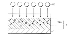
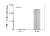
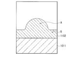
- FIG. 3 is a schematic cross-sectional view for explaining the oxide semiconductor film etching method according to the first embodiment of the present disclosure. It is a cross-sectional schematic diagram showing the process of following FIG. 1A. It is a cross-sectional schematic diagram showing the process of following FIG. 1B. It is a characteristic view showing the change of the film composition before and after general etching. It is a schematic diagram of the TEM image of the ITO film after H 2 plasma irradiation. It is a figure showing the composition ratio of In and O in A and B shown in FIG. 3A.
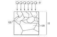
- FIG. 5 is a schematic diagram showing a change in film structure of an oxide semiconductor film due to irradiation with a rare gas.
- FIG. 4C is a schematic diagram illustrating a change in film structure of an oxide semiconductor film due to irradiation with a rare gas, which is subsequent to FIG. 4B.
- FIG. 7 is a schematic cross-sectional view for explaining the oxide semiconductor film etching method according to the second embodiment of the present disclosure. It is a cross-sectional schematic diagram showing the process of following FIG. 5A.
- FIG. 6 is a schematic cross-sectional view showing an etching process of an oxide semiconductor film according to a third embodiment. It is a cross-sectional schematic diagram showing the process of following FIG. 6A.
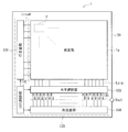
- FIG. 2 is a block diagram showing a configuration of an image sensor using an oxide semiconductor film processed by using the etching method shown in FIGS. 1A to 1C.
- FIG. 8 is a schematic cross-sectional view of a photoelectric conversion element used in the image pickup element shown in FIG. 7. It is a figure explaining the structure of the electronic device using the image pick-up element shown in FIG.
- FIG. 2 is a schematic cross-sectional view of a reflective display device using an oxide semiconductor film processed by using the etching method shown in FIGS. 1A to 1C and the like. It is a figure which shows an example of a schematic structure of an endoscopic surgery system.
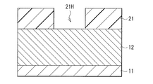
- First Embodiment> 1A to 1C are schematic cross-sectional views showing an etching process of an oxide semiconductor film (oxide semiconductor film 12) according to the first embodiment of the present disclosure.
- the oxide semiconductor film 12 is used, for example, as an electrode constituting various displays such as a flat panel display and a touch panel, devices such as a solar cell and a light emitting diode (LED).
- the oxide semiconductor film 12 is also used as an electromagnetic shield, an antireflection film, and the like.
- the etching method of the present disclosure is suitably used, for example, for patterning the oxide semiconductor film 12 forming an electrode.
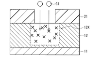
- the deterioration layer 12X is formed in the oxide semiconductor film 12 by modifying the oxide semiconductor film 12 with a rare gas G1 (first rare gas), and then a rare gas different from the rare gas G1 is used. Sputtering is performed using the gas G2 (second rare gas) to process the oxide semiconductor film 12 into a desired shape.
- a method for etching the oxide semiconductor film 12 will be described with reference to FIGS. 1A to 1C.
- the oxide semiconductor film 12 is formed on the supporting substrate 11 by using, for example, a dry method or a wet method.
- the dry method include a physical vapor deposition method (PVD method) and a chemical vapor deposition method (CVD method).
- PVD method physical vapor deposition method
- CVD method chemical vapor deposition method
- a film forming method using the principle of the PVD method a vacuum evaporation method using resistance heat or high frequency heating, an EB (electron beam) evaporation method, various sputtering methods (magnetron sputtering method or high frequency sputtering method), ion plating Method, laser ablation method, molecular beam epitaxy method, and laser transfer method.
- Examples of the film forming method using the principle of the CVD method include a plasma CVD method, a thermal CVD method, a metal organic (MO) CVD method, and an optical CVD method.
- Examples of the wet method include an electroplating method, an electroless plating method, a spin coating method, an inkjet method, a spray coating method, a stamping method, a microcontact printing method, a flexographic printing method, an offset printing method, a gravure printing method, a dipping method and the like.
- the oxide semiconductor film 12 is used, for example, as an electrode forming various devices.
- Specific materials include, for example, indium oxide, indium-tin oxide (Indium Tin Oxide; ITO, including Sn-doped In 2 O 3 , crystalline ITO and amorphous ITO), and zinc oxide to which indium is added as a dopant.
- ITO Indium Tin Oxide
- ITO including Sn-doped In 2 O 3 , crystalline ITO and amorphous ITO
- zinc oxide to which indium is added as a dopant.
- Indium-Zinc Oxide Indium-Zinc Oxide (IZO), Indium-Gallium Oxide (IGO) made by adding Indium as a dopant to gallium oxide, Indium-Gallium-Zinc Oxide made by adding indium and gallium as dopants in zinc oxide (IGZO, In-GaZnO 4 ), indium-tin-zinc oxide (ITZO) obtained by adding indium and tin as a dopant to zinc oxide, IFO (F-doped In 2 O 3 ), tin oxide (SnO 2 ), ATO (Sb-doped SnO 2 ), FTO (F-doped SnO 2 ), zinc oxide (including ZnO doped with other elements), aluminum-zinc oxide (AZO) obtained by adding aluminum as a dopant to zinc oxide, zinc oxide Gallium-zinc oxide (GZO) in which gallium is added as a dopant, titanium oxide (TiO 2 ), niobium-
- a noble gas G1 is irradiated to form an altered layer 12X on the oxide semiconductor film 12.
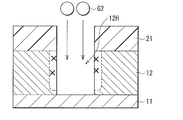
- the noble gas G2 is irradiated to sputter the altered layer 12X.
- the altered layer 12X is removed and the oxide semiconductor film 12 is etched.
- the rare gas G1 and the rare gas G2 are selected from helium (He), neon (Ne), argon (Ar), krypton (Kr), and xenon (Xe).
- a rare gas having a small molecular weight it is possible to penetrate deeply in the thickness direction of the oxide semiconductor film 12, and the altered layer 12X can be formed deep in the oxide semiconductor film 12.
- the rare gas G2 for sputtering the altered layer 12X it is preferable to use a rare gas having a larger molecular weight than the rare gas G1. Since the rare gas having a large molecular weight has a high sputter rate, it is possible to increase the etching rate.
- the rare gas G1 is preferably selected from helium (He) or neon (Ne).
- the rare gas G2 is preferably selected from neon (Ne), argon (Ar) and xenon (Xe).
- FIG. 2 shows the results of measuring the In ratio in the ITO film before and after etching using H 2 /Ar plasma under the measurement condition In 3d 5/2 using X-ray photoelectron spectroscopy (XPS).
- XPS X-ray photoelectron spectroscopy
- FIG. 3A schematically shows a TEM image of the ITO film 1012 formed on the substrate 1011 after the H 2 plasma irradiation.
- the oxide semiconductor film such as ITO
- H 2 plasma a bump-like altered layer is formed on the surface of the oxide semiconductor film as shown in FIG. 3A.
- FIG. 3B shows the results of measuring the In and O concentrations in the altered layer portion (A) and the ITO film portion (B) other than the altered layer shown in FIG. 3A using energy dispersive X-ray analysis (EXD). It is a representation. It can be seen that the In concentration is higher in the altered layer portion (A) than in the ITO film portion (B) other than the altered layer, and the altered layer is formed by In aggregation.
- EXD energy dispersive X-ray analysis
- oxide semiconductor film when the oxide semiconductor film is etched using hydrogen plasma, for example, in the ITO film, O atoms are desorbed from ITO by the penetration of H atoms, and the surface becomes In-rich. In the oxide semiconductor film whose surface is In-rich, for example, the insulating property is lowered.
- An oxide semiconductor is used as an electrode material of a device as described above.
- an upper electrode and a lower electrode that are arranged to face each other with a display layer between them are composed of an oxide semiconductor film, and the oxide semiconductor film is used as described above.
- the composition change of the oxide semiconductor film as described above causes a short circuit between the upper electrode and the lower electrode.
- the oxide semiconductor film 12 is etched using two kinds of rare gas G1 and rare gas G2. Specifically, the deteriorated layer 12X is formed on the oxide semiconductor film 12 by irradiating the rare gas G1 having a smaller molecular weight, and then the deteriorated layer 12X is sputtered by irradiating the rare gas G2 having a larger molecular weight than the rare gas G1. I decided to do it.
- FIG. 4A to FIG. 4C schematically show changes in the crystal structure of the surface of the oxide semiconductor film 12 depending on the dose of the ions G + confirmed by TEM.
- the oxide semiconductor film 12 has a plurality of crystal grains 121 and crystal grain boundaries 122 therein.
- FIG. 4A when the dose of ions G + is small (for example, less than Ion dose: 1 ⁇ 10 17 ions/cm 2 ), a change in the crystal structure of the surface of the oxide semiconductor film is observed. Absent.
- new crystal grains 121 and crystal grain boundaries 122 are formed on the surface of the oxide semiconductor film. become. That is, as shown in FIGS.
- the altered layer 12X formed in this embodiment is a crystal grain boundary 122 due to the penetration of the ion G + into the oxide semiconductor film 12 and a crystallinity disorder due to an increase in the crystal grain boundary 122.
- desorption of oxygen is unlikely to occur and the composition of the oxide semiconductor film is constant over the film thickness direction. Has become.
- the formation of the deteriorated layer 12X on the oxide semiconductor film 12 using the two kinds of rare gases G1 and G2 and The altered layer 12X was sputtered. Accordingly, it is possible to suppress the change over time in the composition ratio of the oxide semiconductor film 12 after sputtering.
- the altered layer 12X formed on the surface is the oxide semiconductor. It is possible to form a deep portion of the film 12.
- the rare gas G2 having a large molecular weight such as Ne, Ar, and Xe is used as the rare gas G2 for sputtering the altered layer 12X, the etching rate of the altered layer 12X is increased. It becomes possible.
- the irradiated rare gas is changed to the rare gas G2 and the altered layer 12X is sputtered.
- the rare gas G1 and the rare gas G2 may be alternately irradiated to alternately form the altered layer 12X and the sputtering thereof. This makes it possible to improve the processing accuracy.
- Second Embodiment> 5A and 5B are schematic cross-sectional views showing the steps of etching the oxide semiconductor film (oxide semiconductor film 12) according to the second embodiment of the present disclosure.
- the method for etching the oxide semiconductor film 12 of this embodiment two kinds of rare gases G1 and G2 are mixed and used, and the altered layer 12X of the oxide semiconductor film 12 is formed and its sputtering is performed in one step. It is a thing.
- a method for etching the oxide semiconductor film 12 will be described with reference to FIGS. 5A and 5B.
- the oxide semiconductor film 12 is formed on the supporting base material 11 by using a dry method or a wet method, for example, as in the first embodiment.
- a mixed gas in which the rare gas G1 and the rare gas G2 are mixed for example, the rare gas G1:the rare gas G2 at a volume ratio in the range of 10:90 to 95:5. Irradiate.
- the altered layer 12X is formed on the oxide semiconductor film 12 and the altered layer 12X is removed by sputtering in one step.
- the rare gas G1 and the rare gas G2 are preferably selected from helium (He) and neon (Ne) having a small molecular weight as the rare gas G1, and the rare gas G2 is neon. It is preferable to select from (Ne), argon (Ar) and xenon (Xe).
- the combination of the rare gas G1 and the rare gas G2 is not particularly limited, and examples thereof include a combination of He/Ne, He/Ar, He/Xe, and the like.
- the mixed gas used in the etching step of the oxide semiconductor film 12 may be a combination of two or more kinds of rare gases as the rare gas G1 and the rare gas G2.
- the etching method of the oxide semiconductor film 12 of the present embodiment since the two kinds of rare gases G1 and G2 are mixed and irradiated to the oxide semiconductor film 12, the altered layer 12X. It is possible to perform the formation and the sputtering thereof in one step. Therefore, in addition to the effect of the first embodiment, there is an effect that the etching process can be simplified.
- Third Embodiment> 6A to 6C are schematic cross-sectional views showing the steps of etching the oxide semiconductor film (oxide semiconductor film 12) according to the third embodiment of the present disclosure.
- the etching method of the oxide semiconductor film 12 of the present disclosure is used, for example, in various devices, electromagnetic shields, antireflection films, and the like as described above.
- TN Transmission Nematic
- STN Super Twist Nematic
- OLEDs Organic Light Emitting Diodes
- PDPs Plasma Display Panels
- FEDs Field Emission Displays
- TFTs thin film transistors
- An example of a specific etching method of the oxide semiconductor film 12 will be described below with reference to FIGS. 6A to 6C.
- a resist film 21 patterned into a predetermined shape is formed on the oxide semiconductor film 12 formed on the supporting base material 11.
- the rare gas G1 is irradiated.
- the rare gas G1 penetrates into the oxide semiconductor film 12 exposed from the opening 21H formed in the resist film 21 to form the altered layer 12X.
- the deteriorated layer 12X is sputtered by irradiating the rare gas G2.
- the altered layer 12X is etched and the opening 12H is formed in the oxide semiconductor film 12.
- the altered layer 12X is a region in which crystal grains and crystal grain boundaries are increased by the invasion of rare gas plasma as described above, and the crystallinity of the oxide semiconductor film 12 is disturbed.
- the altered layer 12X also exists on the side surface of the pattern formed by etching and on the bottom surface of the opening formed by etching when the etching is stopped midway.
- the resist film 21 patterned into a desired shape is formed on the oxide semiconductor film 12
- two layers of the rare gas G1 and the rare gas G2 are used to change the altered layer 12X into the oxide semiconductor film 12.
- the altered layer 12X are sputtered. Accordingly, etching can be performed without changing the composition of the oxide semiconductor film 12, and it is possible to suppress the change over time in the composition ratio of the oxide semiconductor film 12. Therefore, deterioration of characteristics of a device including the oxide semiconductor film 12 can be prevented.
- the oxide semiconductor film 12 processed by using the etching method described in the first embodiment (or the second embodiment) can be applied to, for example, the electronic device described below.
- FIG. 7 is an overall configuration of an image sensor (image sensor 1) using the oxide semiconductor film 12 processed by using the etching method described in the first embodiment (or the second embodiment). Is represented.
- the image pickup device 1 is a CMOS image sensor, has a pixel portion 1a as an image pickup area on a semiconductor substrate 30, and, for example, a row scanning portion 131, a horizontal selection portion 133, in a peripheral region of the pixel portion 1a. It has a peripheral circuit section 130 including a column scanning section 134 and a system control section 132.
- the method for etching an oxide semiconductor film according to the first embodiment described above is suitable for processing the pair of electrodes (the lower electrode 41 and the upper electrode 45) and the charge storage layer 43 that form the organic photoelectric conversion section 40, for example. Used (see FIG. 8 for both).
- the image sensor 1 will be described below.
- the pixel unit 1a has, for example, a plurality of unit pixels P (corresponding to the photoelectric conversion element 10) arranged two-dimensionally in a matrix.
- a pixel drive line Lread (specifically, a row selection line and a reset control line) is wired for each pixel row, and a vertical signal line Lsig is wired for each pixel column.
- the pixel drive line Lread transmits a drive signal for reading a signal from a pixel.
- One end of the pixel drive line Lread is connected to the output end corresponding to each row of the row scanning unit 131.
- the row scanning unit 131 is a pixel driving unit that includes a shift register, an address decoder, and the like, and drives each unit pixel P of the pixel unit 1a, for example, in a row unit.
- the signal output from each unit pixel P of the pixel row selectively scanned by the row scanning unit 131 is supplied to the horizontal selection unit 133 through each of the vertical signal lines Lsig.
- the horizontal selection unit 133 is configured by an amplifier, a horizontal selection switch, and the like provided for each vertical signal line Lsig.
- the column scanning unit 134 is composed of a shift register, an address decoder, and the like, and sequentially drives the horizontal selection switches of the horizontal selection unit 133 while scanning them. By the selective scanning by the column scanning unit 134, the signal of each pixel transmitted through each of the vertical signal lines Lsig is sequentially output to the horizontal signal line 135 and transmitted to the outside of the semiconductor substrate 30 through the horizontal signal line 135. ..
- the circuit portion including the row scanning unit 131, the horizontal selection unit 133, the column scanning unit 134, and the horizontal signal line 135 may be directly formed on the semiconductor substrate 30, or may be provided in the external control IC. May be Further, those circuit portions may be formed on another substrate connected by a cable or the like.
- the system control unit 132 receives a clock given from the outside of the semiconductor substrate 30, data for instructing an operation mode, and outputs data such as internal information of the image pickup device 1.
- the system control unit 132 further includes a timing generator that generates various timing signals, and the row scanning unit 131, the horizontal selection unit 133, the column scanning unit 134, and the like based on the various timing signals generated by the timing generator. Performs drive control of peripheral circuits.
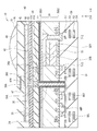
- FIG. 8 schematically illustrates an example of a cross-sectional configuration of the photoelectric conversion element 10 used as one pixel (unit pixel P) in the image pickup element 1.
- the photoelectric conversion element 10 is, for example, a so-called vertical direction spectral type in which one organic photoelectric conversion section 40 and two inorganic photoelectric conversion sections 32B and 32R are vertically stacked.
- the organic photoelectric conversion section 40 is provided on the first surface (back surface) 30S1 side of the semiconductor substrate 30.
- the inorganic photoelectric conversion parts 32B and 32R are embedded in the semiconductor substrate 30 and are stacked in the thickness direction of the semiconductor substrate 30.
- the organic photoelectric conversion section 40 has a photoelectric conversion layer 44 formed of an organic material between a lower electrode 41 and an upper electrode 45 which are arranged to face each other.
- the photoelectric conversion layer 44 includes a p-type semiconductor and an n-type semiconductor, and has a bulk heterojunction structure in the layer.
- the bulk heterojunction structure is a p/n junction surface formed by mixing p-type semiconductors and n-type semiconductors.
- the lower electrode 41 is composed of a plurality of electrodes (readout electrode 41A and storage electrode 41B) for each pixel, and the lower electrode 41 and the photoelectric conversion layer 44 are provided. And an insulating layer 42 and a charge storage layer 43 in this order. An opening 42H is provided in the insulating layer 42 on the read electrode 41A, and the read electrode 41A is electrically connected to the charge storage layer 43 through the opening 42H.
- the organic photoelectric conversion unit 40 and the inorganic photoelectric conversion units 32B and 32R selectively detect light in different wavelength ranges and perform photoelectric conversion. For example, the organic photoelectric conversion unit 40 acquires a green (G) color signal. In the inorganic photoelectric conversion units 32B and 32R, blue (B) and red (R) color signals are respectively acquired due to the difference in absorption coefficient. As a result, the photoelectric conversion element 10 can acquire a plurality of types of color signals in one pixel without using a color filter.
- the multilayer wiring layer 50 has, for example, a configuration in which wiring layers 51, 52, 53 are stacked in an insulating layer 54.
- the first surface 30S1 side of the semiconductor substrate 30 is represented as the light incident side S1
- the second surface 30S2 side is represented as the wiring layer side S2.
- the organic photoelectric conversion section 40 has a configuration in which the lower electrode 41, the charge storage layer 43, the photoelectric conversion layer 44, and the upper electrode 45 are stacked in this order from the first surface 30S1 side of the semiconductor substrate 30. doing.
- An insulating layer 42 is provided between the lower electrode 41 and the charge storage layer 43.
- the read electrode 41A is electrically connected to the photoelectric conversion layer 44 through the opening 42H provided in the insulating layer 42 as described above.
- the fixed charges 33, the dielectric layer 34, and the interlayer insulating layer 37 are provided between the first surface 30S1 of the semiconductor substrate 30 and the lower electrode 41, for example.
- a protective layer 46 is provided on the upper electrode 45. In the protective layer 46, for example, a light shielding film 47 is provided on the read electrode 41A.
- Optical members such as a flattening layer (not shown) and an on-chip lens 48 are provided above the protective layer 46.
- a through electrode 36 is provided between the first surface 30S1 and the second surface 30S2 of the semiconductor substrate 30.
- the organic photoelectric conversion section 40 is connected to the gate Gamp of the amplifier transistor AMP and one source/drain region 36B of the reset transistor RST (reset transistor Tr1rst) also serving as the floating diffusion FD1 via the through electrode 36. Accordingly, in the photoelectric conversion element 10, the charges generated in the organic photoelectric conversion section 40 on the first surface 30S1 side of the semiconductor substrate 30 are satisfactorily transferred to the second surface 30S2 side of the semiconductor substrate 30 via the through electrode 36. , It is possible to improve the characteristics.
- the image pickup device 1 described above can be applied to various electronic devices such as an image pickup device such as a digital still camera and a digital video camera, a mobile phone having an image pickup function, or another device having an image pickup function. ..
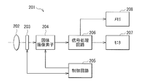
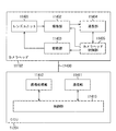
- FIG. 9 is a block diagram showing a configuration example of an imaging device (imaging device 201) as an electronic device to which the present technology is applied.
- the image pickup device 201 shown in FIG. 9 includes an optical system 202, a shutter device 203, a solid-state image pickup element 204, a control circuit 20, a signal processing circuit 206, a monitor 207, and a memory 208, and can pick up still images and moving images. It is something.
- the optical system 202 is configured to have one or a plurality of lenses, guides light (incident light) from a subject to the solid-state image sensor 204, and forms an image on the light-receiving surface of the solid-state image sensor 204.
- the shutter device 203 is arranged between the optical system 202 and the solid-state image sensor 204, and controls the light irradiation period and the light-shielding period of the solid-state image sensor 204 under the control of the control circuit 205.
- the solid-state image sensor 204 is composed of a package including the image sensor 1 described above.
- the solid-state image sensor 204 accumulates signal charges for a certain period according to the light imaged on the light receiving surface via the optical system 202 and the shutter device 203.
- the signal charge accumulated in the solid-state image sensor 204 is transferred according to the drive signal (timing signal) supplied from the control circuit 205.
- the control circuit 205 outputs a drive signal for controlling the transfer operation of the solid-state image sensor 204 and the shutter operation of the shutter device 203 to drive the solid-state image sensor 204 and the shutter device 203.
- the signal processing circuit 206 performs various kinds of signal processing on the signal charges output from the solid-state image sensor 204.
- An image (image data) obtained by the signal processing performed by the signal processing circuit 206 is supplied to the monitor 207 and displayed, or supplied to the memory 208 and stored (recorded).
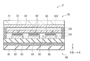
- FIG. 10 shows a schematic configuration of the reflective display device 2.
- the reflective display device 2 is an electrophoretic display that produces a contrast by utilizing an electrophoretic phenomenon, and a display layer provided between the drive substrate 60 and the counter substrate 70 has an electrophoretic element (electrophoretic element). 80) is used.
- the oxide semiconductor film etching method according to the first embodiment or the like is suitably used, for example, in processing the counter electrode 72 forming the counter substrate 70. It should be noted that FIG. 10 schematically shows the configuration of the reflective display device 2, and differs from the actual size and shape.
- a drive substrate 60 and a counter substrate 70 are arranged to face each other with an electrophoretic element 80 interposed therebetween, and a display surface is provided on the counter substrate 70 side.
- the phrase “having a display surface on the counter substrate 70 side” means that an image is displayed toward the counter substrate 70 side (a user can view the image from the counter substrate 70 side).
- the drive substrate 60 has, for example, a thin film transistor (TFT) 62, a protective layer 63, a flattening insulating layer 64, and a pixel electrode 65 formed in this order on one surface of a support base 61.
- TFT thin film transistor
- the TFT 62 and the pixel electrode 65 are, for example, dividedly arranged and divided in a matrix or a segment according to a pixel pattern or the like.
- the counter substrate 70 has, for example, a support base 71 and a counter electrode 72, and the counter electrode 72 is provided on the surface of the support base 71 facing the drive substrate 60.
- the counter electrode 72 may be arranged in a matrix or a segment like the pixel electrode 65.
- the electrophoretic element 80 includes electrophoretic particles 82 and a porous layer 83 in an insulating liquid 81, as shown in FIG.
- the electrophoretic particles 82 are dispersed in the insulating liquid 81, and the porous layer 83 includes, for example, a fibrous structure and non-electrophoretic particles, and has a plurality of pores 833.
- a space between the drive substrate 60 and the counter substrate 70 is maintained between the drive substrate 60 and the counter substrate 70, and a space between the drive substrate 60 and the counter substrate 70 is provided for each pixel, for example.
- a partition wall 85 for partitioning is provided.
- the configuration of the reflective display device 2 shown in FIG. 10 is an example, and various modifications are possible.
- an optical member such as a wavelength conversion layer that converts a wavelength in the invisible region into a wavelength in the visible region may be provided on the display surface side of the counter substrate 70.
- the image sensor 1 shown in FIG. 7 as the above-mentioned application example 1 can be applied to the following products, for example.
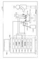
- FIG. 11 is a diagram showing an example of a schematic configuration of an endoscopic surgery system to which the technology according to the present disclosure (the present technology) can be applied.
- FIG. 11 illustrates a situation in which an operator (doctor) 11131 is operating on a patient 11132 on a patient bed 11133 using the endoscopic surgery system 11000.
- the endoscopic surgery system 11000 includes an endoscope 11100, other surgical tools 11110 such as a pneumoperitoneum tube 11111 and an energy treatment tool 11112, and a support arm device 11120 that supports the endoscope 11100.
- a cart 11200 on which various devices for endoscopic surgery are mounted.
- the endoscope 11100 includes a lens barrel 11101 into which a region having a predetermined length from the distal end is inserted into the body cavity of the patient 11132, and a camera head 11102 connected to the base end of the lens barrel 11101.
- the endoscope 11100 configured as a so-called rigid endoscope having the rigid barrel 11101 is illustrated, but the endoscope 11100 may be configured as a so-called flexible mirror having a flexible barrel. Good.
- An opening in which an objective lens is fitted is provided at the tip of the lens barrel 11101.
- a light source device 11203 is connected to the endoscope 11100, and light generated by the light source device 11203 is guided to the tip of the lens barrel by a light guide extending inside the lens barrel 11101. It is irradiated toward the observation target in the body cavity of the patient 11132 via the lens.
- the endoscope 11100 may be a direct-viewing endoscope, or may be a perspective or side-viewing endoscope.
- An optical system and an image pickup device are provided inside the camera head 11102, and the reflected light (observation light) from the observation target is focused on the image pickup device by the optical system.
- the observation light is photoelectrically converted by the imaging element, and an electric signal corresponding to the observation light, that is, an image signal corresponding to the observation image is generated.
- the image signal is transmitted as RAW data to a camera control unit (CCU: Camera Control Unit) 11201.
- CCU Camera Control Unit
- the CCU 11201 is composed of a CPU (Central Processing Unit), a GPU (Graphics Processing Unit), and the like, and centrally controls the operations of the endoscope 11100 and the display device 11202. Further, the CCU 11201 receives the image signal from the camera head 11102, and performs various image processing on the image signal, such as development processing (demosaic processing), for displaying an image based on the image signal.
- CPU Central Processing Unit
- GPU Graphics Processing Unit
- the display device 11202 displays an image based on the image signal subjected to the image processing by the CCU 11201 under the control of the CCU 11201.
- the light source device 11203 is composed of a light source such as an LED (light emitting diode), and supplies irradiation light to the endoscope 11100 when photographing a surgical site or the like.
- a light source such as an LED (light emitting diode)
- the input device 11204 is an input interface for the endoscopic surgery system 11000.
- the user can input various kinds of information and instructions to the endoscopic surgery system 11000 via the input device 11204.
- the user inputs an instruction to change the imaging conditions (type of irradiation light, magnification, focal length, etc.) by the endoscope 11100.
- the treatment instrument control device 11205 controls driving of the energy treatment instrument 11112 for cauterization of tissue, incision, sealing of blood vessel, or the like.
- the pneumoperitoneum device 11206 is used to inflate the body cavity of the patient 11132 through the pneumoperitoneum tube 11111 in order to inflate the body cavity of the patient 11132 for the purpose of securing the visual field by the endoscope 11100 and the working space of the operator.
- the recorder 11207 is a device capable of recording various information regarding surgery.
- the printer 11208 is a device capable of printing various information regarding surgery in various formats such as text, images, and graphs.
- the light source device 11203 that supplies irradiation light to the endoscope 11100 when imaging a surgical site can be configured by, for example, an LED, a laser light source, or a white light source configured by a combination thereof.
- a white light source is configured by a combination of RGB laser light sources, the output intensity and output timing of each color (each wavelength) can be controlled with high accuracy, so that the light source device 11203 adjusts the white balance of the captured image. It can be carried out.
- the laser light from each of the RGB laser light sources is irradiated on the observation target in a time-division manner, and the drive of the image pickup device of the camera head 11102 is controlled in synchronization with the irradiation timing, so that each of the RGB can be handled. It is also possible to take the captured image in a time division manner. According to this method, a color image can be obtained without providing a color filter on the image sensor.
- the drive of the light source device 11203 may be controlled so as to change the intensity of the output light at predetermined time intervals.
- the driving of the image sensor of the camera head 11102 in synchronization with the timing of changing the intensity of the light to acquire an image in a time-division manner and combining the images, a high dynamic image without so-called blackout and overexposure is obtained. An image of the range can be generated.
- the light source device 11203 may be configured to be able to supply light in a predetermined wavelength band corresponding to special light observation.
- special light observation for example, by utilizing the wavelength dependence of absorption of light in body tissues, by irradiating a narrow band of light as compared with the irradiation light (that is, white light) during normal observation, the mucosal surface layer
- the so-called narrow band imaging is performed in which a predetermined tissue such as blood vessel is imaged with high contrast.
- fluorescence observation in which an image is obtained by fluorescence generated by irradiating the excitation light may be performed.
- the excitation light corresponding to the fluorescence wavelength of the reagent can be irradiated to obtain a fluorescence image or the like.
- the light source device 11203 may be configured to be capable of supplying narrowband light and/or excitation light compatible with such special light observation.
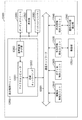
- FIG. 12 is a block diagram showing an example of the functional configuration of the camera head 11102 and the CCU 11201 shown in FIG.
- the camera head 11102 includes a lens unit 11401, an imaging unit 11402, a driving unit 11403, a communication unit 11404, and a camera head control unit 11405.
- the CCU 11201 has a communication unit 11411, an image processing unit 11412, and a control unit 11413.
- the camera head 11102 and the CCU 11201 are communicably connected to each other via a transmission cable 11400.
- the lens unit 11401 is an optical system provided at the connecting portion with the lens barrel 11101.
- the observation light taken from the tip of the lens barrel 11101 is guided to the camera head 11102 and enters the lens unit 11401.
- the lens unit 11401 is configured by combining a plurality of lenses including a zoom lens and a focus lens.
- the number of image pickup devices forming the image pickup unit 11402 may be one (so-called single-plate type) or plural (so-called multi-plate type).
- each image pickup element may generate image signals corresponding to RGB, and these may be combined to obtain a color image.
- the image capturing unit 11402 may be configured to have a pair of image capturing elements for respectively acquiring image signals for the right eye and the left eye corresponding to 3D (dimensional) display.
- the 3D display enables the operator 11131 to more accurately understand the depth of the living tissue in the operation site.
- a plurality of lens units 11401 may be provided corresponding to each image pickup element.
- the image pickup unit 11402 does not necessarily have to be provided in the camera head 11102.
- the imaging unit 11402 may be provided inside the lens barrel 11101 immediately after the objective lens.
- the drive unit 11403 is composed of an actuator, and moves the zoom lens and the focus lens of the lens unit 11401 by a predetermined distance along the optical axis under the control of the camera head control unit 11405. Accordingly, the magnification and focus of the image captured by the image capturing unit 11402 can be adjusted appropriately.
- the communication unit 11404 is composed of a communication device for transmitting and receiving various information to and from the CCU11201.
- the communication unit 11404 transmits the image signal obtained from the imaging unit 11402 as RAW data to the CCU 11201 via the transmission cable 11400.
- the communication unit 11404 receives a control signal for controlling the driving of the camera head 11102 from the CCU 11201, and supplies it to the camera head control unit 11405.
- the control signal includes, for example, information specifying a frame rate of a captured image, information specifying an exposure value at the time of capturing, and/or information specifying a magnification and a focus of the captured image. Contains information about the condition.
- the image capturing conditions such as the frame rate, the exposure value, the magnification, and the focus may be appropriately designated by the user, or may be automatically set by the control unit 11413 of the CCU 11201 based on the acquired image signal. Good. In the latter case, the so-called AE (Auto Exposure) function, AF (Auto Focus) function, and AWB (Auto White Balance) function are mounted on the endoscope 11100.
- the camera head controller 11405 controls driving of the camera head 11102 based on a control signal from the CCU 11201 received via the communication unit 11404.
- the communication unit 11411 is composed of a communication device for transmitting and receiving various information to and from the camera head 11102.
- the communication unit 11411 receives the image signal transmitted from the camera head 11102 via the transmission cable 11400.
- the communication unit 11411 transmits a control signal for controlling the driving of the camera head 11102 to the camera head 11102.
- the image signal and the control signal can be transmitted by electric communication, optical communication, or the like.
- the image processing unit 11412 performs various types of image processing on the image signal that is the RAW data transmitted from the camera head 11102.
- the control unit 11413 performs various controls regarding imaging of a surgical site or the like by the endoscope 11100 and display of a captured image obtained by imaging the surgical site or the like. For example, the control unit 11413 generates a control signal for controlling the driving of the camera head 11102.
- control unit 11413 causes the display device 11202 to display a captured image of the surgical site or the like based on the image signal subjected to the image processing by the image processing unit 11412.
- the control unit 11413 may recognize various objects in the captured image using various image recognition techniques.
- the control unit 11413 detects a surgical instrument such as forceps, a specific living body part, bleeding, and a mist when the energy treatment instrument 11112 is used, by detecting the shape and color of the edge of the object included in the captured image. Can be recognized.
- the control unit 11413 may use the recognition result to superimpose and display various types of surgery support information on the image of the operation unit. By displaying the surgery support information in a superimposed manner and presenting it to the operator 11131, the burden on the operator 11131 can be reduced, and the operator 11131 can reliably proceed with the surgery.
- a transmission cable 11400 that connects the camera head 11102 and the CCU 11201 is an electric signal cable compatible with electric signal communication, an optical fiber compatible with optical communication, or a composite cable of these.
- wired communication is performed using the transmission cable 11400, but communication between the camera head 11102 and the CCU 11201 may be performed wirelessly.
- the technology according to the present disclosure can be applied to the imaging unit 11402 among the configurations described above.
- the detection accuracy is improved.
- the technology according to the present disclosure can be applied to various products.
- the technology according to the present disclosure can be applied to any type of movement of an automobile, an electric vehicle, a hybrid electric vehicle, a motorcycle, a bicycle, a personal mobility, an airplane, a drone, a ship, a robot, a construction machine, an agricultural machine (tractor), and the like. It may be realized as a device mounted on the body.
- FIG. 13 is a block diagram showing a schematic configuration example of a vehicle control system that is an example of a mobile body control system to which the technology according to the present disclosure can be applied.
- the vehicle control system 12000 includes a plurality of electronic control units connected via a communication network 12001.
- the vehicle control system 12000 includes a drive system control unit 12010, a body system control unit 12020, a vehicle exterior information detection unit 12030, a vehicle interior information detection unit 12040, and an integrated control unit 12050.
- a microcomputer 12051, a voice image output unit 12052, and an in-vehicle network I/F (interface) 12053 are shown as a functional configuration of the integrated control unit 12050.
- the drive system control unit 12010 controls the operation of devices related to the drive system of the vehicle according to various programs.
- the drive system control unit 12010 includes a drive force generation device for generating a drive force of a vehicle such as an internal combustion engine or a drive motor, a drive force transmission mechanism for transmitting the drive force to wheels, and a steering angle of the vehicle. It functions as a steering mechanism for adjusting and a control device such as a braking device for generating a braking force of the vehicle.
- the body system control unit 12020 controls the operation of various devices mounted on the vehicle body according to various programs.
- the body system control unit 12020 functions as a keyless entry system, a smart key system, a power window device, or a control device for various lamps such as a head lamp, a back lamp, a brake lamp, a winker, or a fog lamp.
- the body system control unit 12020 may receive radio waves or signals of various switches transmitted from a portable device that substitutes for a key.
- the body system control unit 12020 receives these radio waves or signals and controls the vehicle door lock device, power window device, lamp, and the like.
- the vehicle exterior information detection unit 12030 detects information outside the vehicle equipped with the vehicle control system 12000.
- the image pickup unit 12031 is connected to the vehicle exterior information detection unit 12030.
- the vehicle exterior information detection unit 12030 causes the image capturing unit 12031 to capture an image of the vehicle exterior and receives the captured image.
- the vehicle exterior information detection unit 12030 may perform object detection processing or distance detection processing such as people, vehicles, obstacles, signs, or characters on the road surface based on the received image.
- the image pickup unit 12031 is an optical sensor that receives light and outputs an electric signal according to the amount of received light.
- the imaging unit 12031 can output the electric signal as an image or can output the information as distance measurement information.
- the light received by the imaging unit 12031 may be visible light or invisible light such as infrared light.
- the in-vehicle information detection unit 12040 detects in-vehicle information.
- a driver state detection unit 12041 that detects the state of the driver is connected.
- the driver state detection unit 12041 includes, for example, a camera that captures an image of the driver, and the in-vehicle information detection unit 12040 determines the degree of tiredness or concentration of the driver based on the detection information input from the driver state detection unit 12041. It may be calculated or it may be determined whether or not the driver is asleep.
- the microcomputer 12051 calculates the control target value of the driving force generation device, the steering mechanism or the braking device based on the information on the inside and outside of the vehicle acquired by the outside information detection unit 12030 or the inside information detection unit 12040, and the drive system control unit.
- a control command can be output to 12010.
- the microcomputer 12051 realizes functions of ADAS (Advanced Driver Assistance System) including collision avoidance or impact mitigation of a vehicle, follow-up traveling based on an inter-vehicle distance, vehicle speed maintenance traveling, a vehicle collision warning, or a vehicle lane departure warning. It is possible to perform cooperative control for the purpose.
- ADAS Advanced Driver Assistance System
- the microcomputer 12051 controls the driving force generation device, the steering mechanism, the braking device, or the like based on the information around the vehicle acquired by the vehicle exterior information detection unit 12030 or the vehicle interior information detection unit 12040, thereby It is possible to perform cooperative control for the purpose of autonomous driving or the like that autonomously travels without depending on operation.
- the microcomputer 12051 can output a control command to the body system control unit 12020 based on the information outside the vehicle acquired by the outside information detection unit 12030.
- the microcomputer 12051 controls the headlamp according to the position of the preceding vehicle or the oncoming vehicle detected by the vehicle exterior information detection unit 12030, and performs cooperative control for the purpose of anti-glare such as switching the high beam to the low beam. It can be carried out.
- the voice image output unit 12052 transmits an output signal of at least one of a voice and an image to an output device capable of visually or audibly notifying information to a passenger of the vehicle or the outside of the vehicle.
- an audio speaker 12061, a display unit 12062, and an instrument panel 12063 are illustrated as output devices.
- the display unit 12062 may include, for example, at least one of an onboard display and a head-up display.
- FIG. 14 is a diagram showing an example of the installation position of the imaging unit 12031.
- the image capturing unit 12031 includes image capturing units 12101, 12102, 12103, 12104, and 12105.
- the imaging units 12101, 12102, 12103, 12104, 12105 are provided at positions such as the front nose of the vehicle 12100, the side mirrors, the rear bumper, the back door, and the upper part of the windshield inside the vehicle.
- the image capturing unit 12101 provided on the front nose and the image capturing unit 12105 provided on the upper part of the windshield in the vehicle interior mainly acquire an image in front of the vehicle 12100.
- the imaging units 12102 and 12103 included in the side mirrors mainly acquire images of the side of the vehicle 12100.
- the image capturing unit 12104 provided on the rear bumper or the back door mainly acquires an image of the rear of the vehicle 12100.
- the imaging unit 12105 provided on the upper part of the windshield in the vehicle interior is mainly used for detecting a preceding vehicle, a pedestrian, an obstacle, a traffic signal, a traffic sign, a lane, or the like.
- FIG. 14 shows an example of the shooting range of the imaging units 12101 to 12104.
- the imaging range 12111 indicates the imaging range of the imaging unit 12101 provided on the front nose
- the imaging ranges 12112 and 12113 indicate the imaging ranges of the imaging units 12102 and 12103 provided on the side mirrors
- the imaging range 12114 indicates The imaging range of the imaging part 12104 provided in a rear bumper or a back door is shown.
- a bird's-eye view image of the vehicle 12100 viewed from above can be obtained.
- At least one of the imaging units 12101 to 12104 may have a function of acquiring distance information.
- at least one of the image capturing units 12101 to 12104 may be a stereo camera including a plurality of image capturing elements or may be an image capturing element having pixels for phase difference detection.
- the microcomputer 12051 based on the distance information obtained from the imaging units 12101 to 12104, the distance to each three-dimensional object within the imaging range 12111 to 12114 and the temporal change of this distance (relative speed with respect to the vehicle 12100). By determining, the closest three-dimensional object on the traveling path of the vehicle 12100, which is traveling in the substantially same direction as the vehicle 12100 at a predetermined speed (for example, 0 km/h or more), can be extracted as the preceding vehicle. it can. Further, the microcomputer 12051 can set an inter-vehicle distance to be secured in advance before the preceding vehicle, and can perform automatic brake control (including follow-up stop control), automatic acceleration control (including follow-up start control), and the like. In this way, it is possible to perform cooperative control for the purpose of autonomous driving or the like that autonomously travels without depending on the operation of the driver.
- automatic brake control including follow-up stop control
- automatic acceleration control including follow-up start control
- the microcomputer 12051 uses the distance information obtained from the image capturing units 12101 to 12104 to convert three-dimensional object data regarding a three-dimensional object into another three-dimensional object such as a two-wheeled vehicle, an ordinary vehicle, a large vehicle, a pedestrian, and a utility pole. It can be classified and extracted and used for automatic avoidance of obstacles. For example, the microcomputer 12051 distinguishes obstacles around the vehicle 12100 into obstacles visible to the driver of the vehicle 12100 and obstacles difficult to see. Then, the microcomputer 12051 determines the collision risk indicating the risk of collision with each obstacle, and when the collision risk is equal to or more than the set value and there is a possibility of collision, the microcomputer 12051 outputs the audio through the audio speaker 12061 and the display unit 12062. A driver can be assisted for collision avoidance by outputting an alarm to the driver and performing forced deceleration or avoidance steering via the drive system control unit 12010.
- At least one of the imaging units 12101 to 12104 may be an infrared camera that detects infrared rays.
- the microcomputer 12051 can recognize the pedestrian by determining whether or not the pedestrian is present in the images captured by the imaging units 12101 to 12104.
- a procedure of extracting a feature point in an image captured by the image capturing units 12101 to 12104 as an infrared camera and a pattern matching process on a series of feature points indicating the contour of an object are performed to determine whether the pedestrian is a pedestrian. It is performed by the procedure of determining.
- the audio image output unit 12052 causes the recognized pedestrian to have a rectangular contour line for emphasis.
- the display unit 12062 is controlled so as to superimpose and display.
- the audio image output unit 12052 may control the display unit 12062 to display an icon indicating a pedestrian or the like at a desired position.
- the oxide semiconductor film etching method of the present disclosure may have the following configurations. According to the following configuration, different rare gases (first rare gas and second rare gas) are used to form the deteriorated layer on the oxide semiconductor film and to sputter the deteriorated layer. Desorption of oxygen from the subsequent oxide semiconductor film is reduced. That is, it is possible to suppress the change over time in the composition ratio of the oxide semiconductor film. Note that the effects described here are not necessarily limited, and may be any effects described in the present disclosure. (1) Forming an altered layer on the oxide semiconductor film using the first rare gas; A method for etching an oxide semiconductor film, wherein the altered layer is sputtered using a second rare gas different from the first rare gas.
- the oxide semiconductor film includes indium oxide, indium-tin oxide (ITO), indium-zinc oxide (IZO), indium-gallium oxide (IGO), indium-gallium-zinc oxide (IGZO, In-GaZnO).
Landscapes
- Engineering & Computer Science (AREA)
- Solid State Image Pick-Up Elements (AREA)
- Drying Of Semiconductors (AREA)
- Physics & Mathematics (AREA)
- Plasma & Fusion (AREA)
- Chemical & Material Sciences (AREA)
- Materials Engineering (AREA)
- Nanotechnology (AREA)
- Thin Film Transistor (AREA)
Abstract
本開示の一実施形態の酸化物半導体膜のエッチング方法は、第1の希ガスを用いて酸化物半導体膜に変質層を形成し、第1の希ガスとは異なる第2の希ガスを用いて変質層をスパッタする。
Description
本開示は、例えば、電子デバイスの電極を構成する酸化物半導体膜のエッチング方法に関する。
窒化シリコン(SiN)膜のエッチング方法として、例えば、非特許文献1では、水素プラズマを照射して表面に変質層を形成したのち、フッ素ラジカル照射して変質層の除去を行うエッチング方法が報告されている。
Sonam D. Sherpa and Alok Ranjan. J. Vac. Sci. Technol. A35 01A102 (2017)
ところが、酸化物半導体膜のエッチングに上記のように水素プラズマを用いた場合、時間の経過と共に酸化物半導体膜の組成が変化し、これを用いたデバイスの特性を劣化させるという問題があった。
酸化物半導体膜の組成比の経時変化を抑制することが可能な酸化物半導体のエッチング方法を提供することが望ましい。
本開示の一実施形態の酸化物半導体膜のエッチング方法は、第1の希ガスを用いて酸化物半導体膜に変質層を形成し、第1の希ガスとは異なる第2の希ガスを用いて変質層をスパッタする。
本開示の一実施形態の酸化物半導体膜のエッチング方法では、第1の希ガスを用いて酸化物半導体膜に変質層を形成したのち、第2の希ガスを用いて変質層をスパッタすることにより、スパッタ後の酸化物半導体膜からの酸素の脱離を防ぐ。
以下、本開示における実施の形態について、図面を参照して詳細に説明する。なお、説明は以下の順序で行う。
1.第1の実施の形態(2種類の希ガスを順番に照射したエッチング方法の例)
1-1.酸化物半導体のエッチング方法
1-2.作用・効果
2.第2の実施の形態(2種類の希ガスを混合して照射したエッチング方法の例)
3.第3の実施の形態(エッチング工程の一具体例)
4.適用例
5.応用例
1.第1の実施の形態(2種類の希ガスを順番に照射したエッチング方法の例)
1-1.酸化物半導体のエッチング方法
1-2.作用・効果
2.第2の実施の形態(2種類の希ガスを混合して照射したエッチング方法の例)
3.第3の実施の形態(エッチング工程の一具体例)
4.適用例
5.応用例
<1.第1の実施の形態>
図1A~図1Cは、本開示の第1の実施の形態に係る酸化物半導体膜(酸化物半導体膜12)のエッチング工程を表した断面模式図である。酸化物半導体膜12は、例えば、フラットパネルディスプレイおよびタッチパネル等の各種ディスプレイ、太陽電池および発光ダイオード(Light Emitting Diode;LED)等のデバイスを構成する電極として用いられるものである。この他、酸化物半導体膜12は、電磁シールドおよび反射防止膜等にも用いられる。本開示のエッチング方法は、例えば、電極を構成する酸化物半導体膜12のパターニング等に好適に用いられるものである。
図1A~図1Cは、本開示の第1の実施の形態に係る酸化物半導体膜(酸化物半導体膜12)のエッチング工程を表した断面模式図である。酸化物半導体膜12は、例えば、フラットパネルディスプレイおよびタッチパネル等の各種ディスプレイ、太陽電池および発光ダイオード(Light Emitting Diode;LED)等のデバイスを構成する電極として用いられるものである。この他、酸化物半導体膜12は、電磁シールドおよび反射防止膜等にも用いられる。本開示のエッチング方法は、例えば、電極を構成する酸化物半導体膜12のパターニング等に好適に用いられるものである。
(1-1.酸化物半導体のエッチング方法)
本実施の形態の酸化物半導体膜12のエッチング方法は、希ガスG1(第1の希ガス)で変質させて酸化物半導体膜12に変質層12Xを形成したのち、希ガスG1とは異なる希ガスG2(第2の希ガス)を用いてスパッタを行い、酸化物半導体膜12を所望の形状に加工するものである。以下に、図1A~図1Cを用いて酸化物半導体膜12のエッチング方法を説明する。
本実施の形態の酸化物半導体膜12のエッチング方法は、希ガスG1(第1の希ガス)で変質させて酸化物半導体膜12に変質層12Xを形成したのち、希ガスG1とは異なる希ガスG2(第2の希ガス)を用いてスパッタを行い、酸化物半導体膜12を所望の形状に加工するものである。以下に、図1A~図1Cを用いて酸化物半導体膜12のエッチング方法を説明する。
まず、図1Aに示したように、支持基材11上に、例えば乾式法あるいは湿式法を用いて酸化物半導体膜12を成膜する。乾式法としては、物理的気相成長法(PVD法)および化学的気相成長法(CVD法)が挙げられる。PVD法の原理を用いた成膜方法としては、抵抗化熱または高周波加熱を用いた真空蒸着法、EB(電子ビーム)蒸着法、各種スパッタリング法(マグネトロンスパッタリング法または高周波スパッタリング法)、イオンプレーティング法、レーザアブレーション法、分子線エピタキシー法、レーザ転写法が挙げられる。CVD法の原理を用いた成膜方法としては、プラズマCVD法、熱CVD法、有機金属(MO)CVD法および光CVD法が挙げられる。湿式法としては、電界メッキ法、無電解メッキ法、スピンコート法、インクジェット法、スプレーコート法、スタンプ法、マイクロコンタクトプリント法、フレキソ印刷法、オフセット印刷法、グラビア印刷法、ディップ法等が挙げられる。酸化物半導体膜12は、上記のように、例えば、各種デバイスを構成する電極として用いられるものである。具体的な材料としては、例えば、酸化インジウム、インジウム-錫酸化物(Indium Tin Oxide;ITO,SnドープのIn2O3、結晶性ITOおよびアモルファスITOを含む)、酸化亜鉛にドーパントとしてインジウムを添加したインジウム-亜鉛酸化物(Indium Zinc Oxide;IZO)、酸化ガリウムにドーパントとしてインジウムを添加したインジウム-ガリウム酸化物(IGO)、酸化亜鉛にドーパントとしてインジウムおよびガリウムを添加したインジウム-ガリウム-亜鉛酸化物(IGZO,In-GaZnO4)、酸化亜鉛にドーパントとしてインジウムおよび錫を添加したインジウム-錫-亜鉛酸化物(ITZO)、IFO(FドープのIn2O3)、酸化錫(SnO2)、ATO(SbドープのSnO2)、FTO(FドープのSnO2)、酸化亜鉛(他元素をドープしたZnOを含む)、酸化亜鉛にドーパントとしてアルミニウムを添加したアルミニウム-亜鉛酸化物(AZO)、酸化亜鉛にドーパントとしてガリウムを添加したガリウム-亜鉛酸化物(GZO)、酸化チタン(TiO2)、酸化チタンにドーパントとしてニオブを添加したニオブ-チタン酸化物(TNO)、酸化アンチモン、スピネル型酸化物およびYbFe2O4構造を有する酸化物が挙げられる。この他、ガリウム酸化物、チタン酸化物、ニオブ酸化物またはニッケル酸化物等を母層とする透明電極材料が挙げられる。
続いて、図1Bに示したように、希ガスG1を照射して酸化物半導体膜12に変質層12Xを形成する。次に、希ガスG2を照射して変質層12Xをスパッタする。これにより、変質層12Xが除去され、酸化物半導体膜12がエッチングされる。
希ガスG1および希ガスG2は、ヘリウム(He)、ネオン(Ne)、アルゴン(Ar)、クリプトン(Kr)およびキセノン(Xe)から選択される。本実施の形態では、変質層12Xを形成する希ガスG1としては、変質層12Xをスパッタする希ガスG2よりも分子量の小さな希ガスを用いることが好ましい。分子量の小さな希ガスを用いることで、酸化物半導体膜12の膜厚方向に深く侵入することが可能となり、酸化物半導体膜12の深くまで変質層12Xを形成することが可能となる。また、変質層12Xをスパッタする希ガスG2は、希ガスG1よりも分子量の大きな希ガスを用いることが好ましい。分子量の大きな希ガスはスパッタレートが高いため、エッチング速度を増速させることが可能となる。以上のことから、希ガスG1としては、ヘリウム(He)またはネオン(Ne)から選択することが好ましい。希ガスG2としては、ネオン(Ne)、アルゴン(Ar)およびキセノン(Xe)から選択することが好ましい。
(1-2.作用・効果)
前述したように、水素プラズマを用いてITOやIGZO等の酸化物半導体膜をエッチングした場合、時間の経過と共に酸化物半導体膜の組成が変化し、これを用いたデバイスの特性を劣化させるという問題がある。
前述したように、水素プラズマを用いてITOやIGZO等の酸化物半導体膜をエッチングした場合、時間の経過と共に酸化物半導体膜の組成が変化し、これを用いたデバイスの特性を劣化させるという問題がある。
図2は、X線光電子分光法(XPS)を用い、測定条件In 3d5/2でのH2/Arプラズマを用いたエッチング前後のITO膜中のInの比率を測定した結果を表したものである。InのBinding energy(eV)は444.11eV、In2O3のBinding energy(eV)は444.32eVとし、In比率はIn/In2O3比で算出した。H2/Arプラズマ照射前と比較して、H2/Arプラズマ照射後のITO膜では、In-In結合が増加していることがわかる。
図3Aは、基板1011上に形成されたITO膜1012のH2プラズマ照射後のTEM画像を模式的に表したものである。ITO等の酸化物半導体膜にH2プラズマを照射した場合、図3Aに示したように、酸化物半導体膜の表面には瘤状の変質層が形成される。図3Bは、エネルギー分散型X線分析(EXD)を用いて、図3Aに示した変質層部分(A)および変質層以外のITO膜部分(B)のInおよびOの濃度を測定した結果を表したものである。変質層以外のITO膜部分(B)と比較して、変質層部分(A)ではIn濃度が高く、変質層はInの凝集によって形成されていることがわかる。
このように、水素プラズマを用いて酸化物半導体膜をエッチングすると、H原子の侵入によって例えばITO膜ではITOからO原子が脱離し、表面がInリッチになる。表面がInリッチになった酸化物半導体膜では、例えば絶縁性が低下する。酸化物半導体は、上記のようにデバイスの電極材料として用いられるが、例えば表示層を間に対向配置される上部電極および下部電極を酸化物半導体膜で構成し、これを上記のように水素プラズマを用いてエッチングした場合、上述したような酸化物半導体膜の組成変化は上部電極と下部電極との間の短絡の原因となる。
これに対して、本実施の形態では、2種類の希ガスG1および希ガスG2を用いて酸化物半導体膜12をエッチングするようにした。具体的には、より分子量の小さな希ガスG1を照射して酸化物半導体膜12に変質層12Xを形成したのち、希ガスG1よりも分子量の大きな希ガスG2を照射して変質層12Xをスパッタするようにした。
図4A~図4Cは、TEMによって確認されるイオンG+の照射量による酸化物半導体膜12の表面の結晶構造の変化を模式的に表したものである。酸化物半導体膜12は内部に複数からなる結晶粒121および結晶粒界122が存在する。図4Aに示したように、イオンG+の照射量が少ない(例えば、Ion dose:1×10¹⁷ion/cm2未満)場合には、酸化物半導体膜の表面の結晶構造に変化は見られない。イオンG+の照射量を増加させる(例えば、Ion dose:1×10¹⁷ion/cm2以上)ことで酸化物半導体膜の表面には新たな結晶粒121および結晶粒界122が形成されるようになる。即ち、図4Bおよび図4Cに示したように、照射量の増加に比例して酸化物半導体膜の表面には結晶粒121および結晶粒界122が増加する。即ち、本実施の形態において形成される変質層12Xは、酸化物半導体膜12へのイオンG+の侵入による結晶粒界122および結晶粒界122の増加による結晶性の乱れであり、上記のような水素イオン(H+)を用いたエッチングによる酸素の脱離等の化学的な変質とは異なり、酸素の脱離は起こりにくく、酸化物半導体膜の組成はその膜厚方向に渡って一定となっている。
以上により、本実施の形態の本実施の形態の酸化物半導体膜12のエッチング方法では、2種類の希ガスG1および希ガスG2を用いて、酸化物半導体膜12への変質層12Xの形成および変質層12Xのスパッタを行うようにした。これにより、スパッタ後の酸化物半導体膜12の組成比の経時変化を抑制することが可能となる。
また、本実施の形態では、変質層12Xを形成する希ガスG1として、例えばHeやNeのように分子量の小さな希ガスを用いるようにしたので、表面に形成される変質層12Xを酸化物半導体膜12の深部まで形成することが可能となる。
更に、本実施の形態では、変質層12Xをスパッタする希ガスG2として、例えば、Ne、ArおよびXeのような分子量の大きな希ガスを用いるようにしたので、変質層12Xのエッチング速度を増速させることが可能となる。
なお、本実施の形態では、酸化物半導体膜12のエッチング方法として、希ガスG1を照射して変質層12Xを形成したのち、照射する希ガスを希ガスG2に替えて変質層12Xをスパッタする、2工程で行うエッチング方法の例を示したがこれに限らない。例えば、希ガスG1と希ガスG2とを交互に照射して、変質層12Xの形成とそのスパッタとを交互に行うようにしてもよい。これにより、加工精度を向上させることが可能となる。
以下、本開示の第2,第3の実施の形態ついて説明する。なお、上記第1の実施の形態と同一の構成要素については同一の符号を付し説明を省略する。
<2.第2の実施の形態>
図5Aおよび図5Bは、本開示の第2の実施の形態に係る酸化物半導体膜(酸化物半導体膜12)のエッチング工程を表した断面模式図である。本実施の形態の酸化物半導体膜12のエッチング方法は、2種類の希ガスG1および希ガスG2を混合して用い、酸化物半導体膜12の変質層12Xの形成およびそのスパッタを1工程で行うものである。以下に、図5Aおよび図5Bを用いて酸化物半導体膜12のエッチング方法を説明する。
図5Aおよび図5Bは、本開示の第2の実施の形態に係る酸化物半導体膜(酸化物半導体膜12)のエッチング工程を表した断面模式図である。本実施の形態の酸化物半導体膜12のエッチング方法は、2種類の希ガスG1および希ガスG2を混合して用い、酸化物半導体膜12の変質層12Xの形成およびそのスパッタを1工程で行うものである。以下に、図5Aおよび図5Bを用いて酸化物半導体膜12のエッチング方法を説明する。
まず、図5Aに示したように、支持基材11上に、例えば、上記第1の実施の形態と同様に、乾式法あるいは湿式法を用いて酸化物半導体膜12を成膜する。続いて、図5Bに示したように、例えば、希ガスG1および希ガスG2を、例えば、希ガスG1:希ガスG2を10:90以上95:5以下の範囲の体積比で混合した混合ガスを照射する。これにより、酸化物半導体膜12への変質層12Xの形成およびスパッタによる変質層12Xの除去が1工程中に行われる。
希ガスG1および希ガスG2は、上記第1の実施の形態と同様に、希ガスG1としては分子量の小さなヘリウム(He)およびネオン(Ne)から選択することが好ましく、希ガスG2としてはネオン(Ne)、アルゴン(Ar)およびキセノン(Xe)から選択することが好ましい。希ガスG1および希ガスG2の組み合わせは特に限定されず、例えば、He/Ne、He/Ar、He/Xe等の組み合わせが挙げられる。また、上記酸化物半導体膜12のエッチング工程において用いられる混合ガスは、上記希ガスG1および希ガスG2として、それぞれ2種類以上の希ガスを組み合わせて用いるようにしてもよい。
以上のように、本実施の形態の酸化物半導体膜12のエッチング方法では、2種類の希ガスG1および希ガスG2を混合して酸化物半導体膜12に照射するようにしたので、変質層12Xの形成およびそのスパッタを1工程で行うことが可能となる。よって、上記第1の実施の形態における効果に加えて、エッチング工程を簡略化することが可能となるという効果を奏する。
<3.第3の実施の形態>
図6A~図6Cは、本開示の第3の実施の形態に係る酸化物半導体膜(酸化物半導体膜12)のエッチング工程を表した断面模式図である。本開示の酸化物半導体膜12のエッチング方法は、上記のように、例えば、各種デバイスや電磁シールドおよび反射防止膜等において用いられるものであり、例えば、ディスプレイ関連では、TN(Twist Nematic)型およびSTN(Super Twist Nematic)型の液晶ディスプレイ、OLED(Organic Light Emitting Diode)、PDP(Plasma Display Panel)、FED(Field Emission Display)および電子ペーパーを構成する電極、薄膜トランジスタ(TFT)およびカラーフィルタの加工に好適に用いられる。以下に、図6A~図6Cを用いて酸化物半導体膜12の具体的なエッチング方法の一例を説明する。
図6A~図6Cは、本開示の第3の実施の形態に係る酸化物半導体膜(酸化物半導体膜12)のエッチング工程を表した断面模式図である。本開示の酸化物半導体膜12のエッチング方法は、上記のように、例えば、各種デバイスや電磁シールドおよび反射防止膜等において用いられるものであり、例えば、ディスプレイ関連では、TN(Twist Nematic)型およびSTN(Super Twist Nematic)型の液晶ディスプレイ、OLED(Organic Light Emitting Diode)、PDP(Plasma Display Panel)、FED(Field Emission Display)および電子ペーパーを構成する電極、薄膜トランジスタ(TFT)およびカラーフィルタの加工に好適に用いられる。以下に、図6A~図6Cを用いて酸化物半導体膜12の具体的なエッチング方法の一例を説明する。
まず、図6Aに示したように、支持基材11上に形成された酸化物半導体膜12上に、所定の形状にパターニングされたレジスト膜21を形成する。続いて、図6Bに示したように、希ガスG1を照射する。これにより、レジスト膜21に形成された開口21Hから露出している酸化物半導体膜12内に希ガスG1が侵入して変質層12Xが形成される。次に、図6Cに示したように、希ガスG2を照射して変質層12Xをスパッタする。これにより、変質層12Xがエッチングされ、酸化物半導体膜12に開口12Hが形成される。
なお、変質層12Xは、上記のように、希ガスプラズマの侵入によって結晶粒および結晶粒界が増加した領域であり、酸化物半導体膜12の結晶性が乱れた領域である。この変質層12Xは、エッチングによって形成されたパターンの側面および、エッチングを途中で止めた場合にはエッチングによって形成される開口の底面にも存在する。
以上のように、酸化物半導体膜12上に所望の形状にパターニングしたレジスト膜21を形成したのち、2種類の希ガスG1および希ガスG2を用いて、酸化物半導体膜12への変質層12Xの形成および変質層12Xのスパッタを行うようにした。これにより、酸化物半導体膜12の組成を変化させることなくエッチングが可能となり、酸化物半導体膜12の組成比の経時変化を抑制することが可能となる。よって、酸化物半導体膜12を用いたデバイスの特性の劣化を防ぐことが可能となる。
<4.適用例>
上記第1の実施の形態(または、第2の実施の形態)において説明したエッチング方法を用いて加工された酸化物半導体膜12は、例えば、以下に説明する電子デバイスに適用することができる。
上記第1の実施の形態(または、第2の実施の形態)において説明したエッチング方法を用いて加工された酸化物半導体膜12は、例えば、以下に説明する電子デバイスに適用することができる。
(適用例1)
図7は、上記第1の実施の形態(または、第2の実施の形態)において説明したエッチング方法を用いて加工された酸化物半導体膜12を用いた撮像素子(撮像素子1)の全体構成を表したものである。この撮像素子1は、CMOSイメージセンサであり、半導体基板30上に、撮像エリアとしての画素部1aを有すると共に、この画素部1aの周辺領域に、例えば、行走査部131、水平選択部133、列走査部134およびシステム制御部132からなる周辺回路部130を有している。上記第1の実施の形態等の酸化物半導体膜のエッチング方法は、例えば、有機光電変換部40を構成する一対の電極(下部電極41および上部電極45)および電荷蓄積層43の加工において好適に用いられる(いずれも、図8参照)。以下に、撮像素子1について説明する。
図7は、上記第1の実施の形態(または、第2の実施の形態)において説明したエッチング方法を用いて加工された酸化物半導体膜12を用いた撮像素子(撮像素子1)の全体構成を表したものである。この撮像素子1は、CMOSイメージセンサであり、半導体基板30上に、撮像エリアとしての画素部1aを有すると共に、この画素部1aの周辺領域に、例えば、行走査部131、水平選択部133、列走査部134およびシステム制御部132からなる周辺回路部130を有している。上記第1の実施の形態等の酸化物半導体膜のエッチング方法は、例えば、有機光電変換部40を構成する一対の電極(下部電極41および上部電極45)および電荷蓄積層43の加工において好適に用いられる(いずれも、図8参照)。以下に、撮像素子1について説明する。
画素部1aは、例えば、行列状に2次元配置された複数の単位画素P(光電変換素子10に相当)を有している。この単位画素Pには、例えば、画素行ごとに画素駆動線Lread(具体的には行選択線およびリセット制御線)が配線され、画素列ごとに垂直信号線Lsigが配線されている。画素駆動線Lreadは、画素からの信号読み出しのための駆動信号を伝送するものである。画素駆動線Lreadの一端は、行走査部131の各行に対応した出力端に接続されている。
行走査部131は、シフトレジスタやアドレスデコーダ等によって構成され、画素部1aの各単位画素Pを、例えば、行単位で駆動する画素駆動部である。行走査部131によって選択走査された画素行の各単位画素Pから出力される信号は、垂直信号線Lsigの各々を通して水平選択部133に供給される。水平選択部133は、垂直信号線Lsigごとに設けられたアンプや水平選択スイッチ等によって構成されている。
列走査部134は、シフトレジスタやアドレスデコーダ等によって構成され、水平選択部133の各水平選択スイッチを走査しつつ順番に駆動するものである。この列走査部134による選択走査により、垂直信号線Lsigの各々を通して伝送される各画素の信号が順番に水平信号線135に出力され、当該水平信号線135を通して半導体基板30の外部へ伝送される。
行走査部131、水平選択部133、列走査部134および水平信号線135からなる回路部分は、半導体基板30上に直に形成されていてもよいし、あるいは外部制御ICに配設されたものであってもよい。また、それらの回路部分は、ケーブル等により接続された他の基板に形成されていてもよい。
システム制御部132は、半導体基板30の外部から与えられるクロックや、動作モードを指令するデータ等を受け取り、また、撮像素子1の内部情報等のデータを出力するものである。システム制御部132はさらに、各種のタイミング信号を生成するタイミングジェネレータを有し、当該タイミングジェネレータで生成された各種のタイミング信号を基に行走査部131、水平選択部133および列走査部134等の周辺回路の駆動制御を行う。
図8は、撮像素子1において1つの画素(単位画素P)として用いられる光電変換素子10の断面構成の一例を模式的に表したものである。光電変換素子10は、例えば、1つの有機光電変換部40と、2つの無機光電変換部32B,32Rとが縦方向に積層された、いわゆる縦方向分光型のものである。有機光電変換部40は、半導体基板30の第1面(裏面)30S1側に設けられている。無機光電変換部32B,32Rは、半導体基板30内に埋め込み形成されており、半導体基板30の厚み方向に積層されている。有機光電変換部40は、対向配置された下部電極41と上部電極45との間に、有機材料を用いて形成された光電変換層44を有する。この光電変換層44は、p型半導体およびn型半導体を含んで構成され、層内にバルクヘテロ接合構造を有する。バルクヘテロ接合構造は、p型半導体およびn型半導体が混ざり合うことで形成されたp/n接合面である。
この光電変換素子10では、有機光電変換部40は、例えば、下部電極41が画素毎に複数の電極(読み出し電極41Aおよび蓄積電極41B)から構成されており、この下部電極41と光電変換層44との間に絶縁層42および電荷蓄積層43を順に有する。絶縁層42には、読み出し電極41A上に開口42Hが設けられており、読み出し電極41Aはこの開口42Hを介して電荷蓄積層43と電気的に接続されている。
有機光電変換部40と、無機光電変換部32B,32Rとは、互いに異なる波長域の光を選択的に検出して光電変換を行うものである。例えば、有機光電変換部40では、緑(G)の色信号を取得する。無機光電変換部32B,32Rでは、吸収係数の違いにより、それぞれ、青(B)および赤(R)の色信号を取得する。これにより、光電変換素子10では、カラーフィルタを用いることなく一つの画素において複数種類の色信号を取得可能となっている。
半導体基板30の第2面(表面)30S2には、例えば、フローティングディフュージョン(浮遊拡散層)FD1,FD2,FD3と、転送トランジスタTr2(縦型)トランジスタおよび転送トランジスタTr3と、アンプトランジスタ(変調素子)AMPと、リセットトランジスタRSTと、選択トランジスタSELと、多層配線層50とが設けられている。多層配線層50は、例えば、配線層51,52,53が絶縁層54内に積層された構成を有している。
なお、図面では、半導体基板30の第1面30S1側を光入射側S1、第2面30S2側を配線層側S2と表している。
有機光電変換部40は、上記のように、下部電極41、電荷蓄積層43、光電変換層44および上部電極45が、半導体基板30の第1面30S1の側からこの順に積層された構成を有している。また、下部電極41と電荷蓄積層43との間には、絶縁層42が設けられている。下部電極41のうち、読み出し電極41Aは、上記のように、絶縁層42に設けられた開口42Hを介して光電変換層44と電気的に接続されている。半導体基板30の第1面30S1と下部電極41との間には、例えば、固定電荷33、誘電体層34および層間絶縁層37とが設けられている。上部電極45の上には、保護層46が設けられている。保護層46内には、例えば、読み出し電極41A上に遮光膜47が設けられている。保護層46の上方には、平坦化層(図示せず)やオンチップレンズ48等の光学部材が配設されている。
半導体基板30の第1面30S1と第2面30S2との間には、貫通電極36が設けられている。有機光電変換部40は、この貫通電極36を介して、アンプトランジスタAMPのゲートGampと、フローティングディフュージョンFD1を兼ねるリセットトランジスタRST(リセットトランジスタTr1rst)の一方のソース/ドレイン領域36Bに接続されている。これにより、光電変換素子10では、半導体基板30の第1面30S1側の有機光電変換部40で生じた電荷を、貫通電極36を介して半導体基板30の第2面30S2側に良好に転送し、特性を高めることが可能となっている。
上述した撮像素子1は、例えば、デジタルスチルカメラやデジタルビデオカメラ等の撮像装置、撮像機能を備えた携帯電話機、または、撮像機能を備えた他の機器といった各種の電子機器に適用することができる。
図9は、本技術を適用した電子機器としての撮像装置(撮像装置201)の構成例を示したブロック図である。
図9に示した撮像装置201は、光学系202、シャッタ装置203、固体撮像素子204、制御回路20、信号処理回路206、モニタ207およびメモリ208を備えており、静止画像および動画像を撮像可能なものである。
光学系202は、1枚または複数枚のレンズを有して構成され、被写体からの光(入射光)を固体撮像素子204に導き、固体撮像素子204の受光面に結像させる。
シャッタ装置203は、光学系202と固体撮像素子204との間に配置され、制御回路205の制御に従って、固体撮像素子204への光照射期間および遮光期間を制御する。
固体撮像素子204は、上述した撮像素子1を含むパッケージにより構成されている。固体撮像素子204は、光学系202およびシャッタ装置203を介して受光面に結像される光に応じて、一定期間、信号電荷を蓄積する。固体撮像素子204に蓄積された信号電荷は、制御回路205から供給される駆動信号(タイミング信号)に従って転送される。
制御回路205は、固体撮像素子204の転送動作およびシャッタ装置203のシャッタ動作を制御する駆動信号を出力して、固体撮像素子204およびシャッタ装置203を駆動する。
信号処理回路206は、固体撮像素子204から出力された信号電荷に対して各種の信号処理を施す。信号処理回路206が信号処理を施すことにより得られた画像(画像データ)は、モニタ207に供給されて表示されたり、メモリ208に供給されて記憶(記録)されたりする。
(適用例2)
図10は、反射型表示装置2の概略構成を表したものである。反射型表示装置2は、電気泳動現象を利用してコントラストを生じさせる電気泳動型ディスプレイであり、駆動基板60と対向基板70との間に設けられる表示層には、電気泳動素子(電気泳動素子80)が用いられている。上記第1の実施の形態等の酸化物半導体膜のエッチング方法は、例えば、対向基板70を構成する対向電極72の加工において好適に用いられる。なお、図10は反射型表示装置2の構成を模式的に表したものであり、実際の寸法、形状とは異なる。
図10は、反射型表示装置2の概略構成を表したものである。反射型表示装置2は、電気泳動現象を利用してコントラストを生じさせる電気泳動型ディスプレイであり、駆動基板60と対向基板70との間に設けられる表示層には、電気泳動素子(電気泳動素子80)が用いられている。上記第1の実施の形態等の酸化物半導体膜のエッチング方法は、例えば、対向基板70を構成する対向電極72の加工において好適に用いられる。なお、図10は反射型表示装置2の構成を模式的に表したものであり、実際の寸法、形状とは異なる。
反射型表示装置2は、例えば、図10に示したように、駆動基板60と対向基板70とが電気泳動素子80を介して対向配置されたものであり、対向基板70側に表示面を有している。この「対向基板70側に表示面を有する」とは、対向基板70側に向かって画像を表示する(ユーザが対向基板70側から画像を視認可能である)という意味である。
駆動基板60は、例えば、支持基体61の一面に薄膜トランジスタ(Thin Film Transistor;TFT)62と、保護層63と、平坦化絶縁層64と、画素電極65とがこの順に形成されたものである。TFT62および画素電極65は、例えば、画素パターン等に応じてマトリクス状またはセグメント状に分割配置および分割形成されている。
対向基板70は、例えば、支持基体71および対向電極72を有し、この対向電極72は支持基体71の駆動基板60との対向面に設けられている。対向電極72は、画素電極65と同様に、マトリクス状またはセグメント状に配置するようにしてもよい。
電気泳動素子80は、図10に示したように、絶縁性液体81中に、泳動粒子82および多孔質層83を備えている。泳動粒子82は、絶縁性液体81中に分散されており、多孔質層83は、例えば、繊維状構造体および非泳動粒子を含んで構成され、複数の細孔833を有している。駆動基板60と対向基板70との間には、例えば、駆動基板60と対向基板70との間の空間を保持すると共に、例えば、駆動基板60と対向基板70との間の空間を画素ごとに区画する隔壁85が設けられている。
なお、図10に示した反射型表示装置2の構成は一例であり、種々の変形が可能である。例えば、対向基板70の表示面側には、例えば、非可視領域の波長を可視領域の波長に変換する波長変換層等の光学部材を設けるようにしてもよい。
なお、上記適用例1として図7に示した撮像素子1は、例えば、以下の製品へ応用することができる。
<5.応用例>
<内視鏡手術システムへの応用例>
本開示に係る技術(本技術)は、様々な製品へ応用することができる。例えば、本開示に係る技術は、内視鏡手術システムに適用されてもよい。
<内視鏡手術システムへの応用例>
本開示に係る技術(本技術)は、様々な製品へ応用することができる。例えば、本開示に係る技術は、内視鏡手術システムに適用されてもよい。
図11は、本開示に係る技術(本技術)が適用され得る内視鏡手術システムの概略的な構成の一例を示す図である。
図11では、術者(医師)11131が、内視鏡手術システム11000を用いて、患者ベッド11133上の患者11132に手術を行っている様子が図示されている。図示するように、内視鏡手術システム11000は、内視鏡11100と、気腹チューブ11111やエネルギー処置具11112等の、その他の術具11110と、内視鏡11100を支持する支持アーム装置11120と、内視鏡下手術のための各種の装置が搭載されたカート11200と、から構成される。
内視鏡11100は、先端から所定の長さの領域が患者11132の体腔内に挿入される鏡筒11101と、鏡筒11101の基端に接続されるカメラヘッド11102と、から構成される。図示する例では、硬性の鏡筒11101を有するいわゆる硬性鏡として構成される内視鏡11100を図示しているが、内視鏡11100は、軟性の鏡筒を有するいわゆる軟性鏡として構成されてもよい。
鏡筒11101の先端には、対物レンズが嵌め込まれた開口部が設けられている。内視鏡11100には光源装置11203が接続されており、当該光源装置11203によって生成された光が、鏡筒11101の内部に延設されるライトガイドによって当該鏡筒の先端まで導光され、対物レンズを介して患者11132の体腔内の観察対象に向かって照射される。なお、内視鏡11100は、直視鏡であってもよいし、斜視鏡又は側視鏡であってもよい。
カメラヘッド11102の内部には光学系及び撮像素子が設けられており、観察対象からの反射光(観察光)は当該光学系によって当該撮像素子に集光される。当該撮像素子によって観察光が光電変換され、観察光に対応する電気信号、すなわち観察像に対応する画像信号が生成される。当該画像信号は、RAWデータとしてカメラコントロールユニット(CCU: Camera Control Unit)11201に送信される。
CCU11201は、CPU(Central Processing Unit)やGPU(Graphics Processing Unit)等によって構成され、内視鏡11100及び表示装置11202の動作を統括的に制御する。さらに、CCU11201は、カメラヘッド11102から画像信号を受け取り、その画像信号に対して、例えば現像処理(デモザイク処理)等の、当該画像信号に基づく画像を表示するための各種の画像処理を施す。
表示装置11202は、CCU11201からの制御により、当該CCU11201によって画像処理が施された画像信号に基づく画像を表示する。
光源装置11203は、例えばLED(light emitting diode)等の光源から構成され、術部等を撮影する際の照射光を内視鏡11100に供給する。
入力装置11204は、内視鏡手術システム11000に対する入力インタフェースである。ユーザは、入力装置11204を介して、内視鏡手術システム11000に対して各種の情報の入力や指示入力を行うことができる。例えば、ユーザは、内視鏡11100による撮像条件(照射光の種類、倍率及び焦点距離等)を変更する旨の指示等を入力する。
処置具制御装置11205は、組織の焼灼、切開又は血管の封止等のためのエネルギー処置具11112の駆動を制御する。気腹装置11206は、内視鏡11100による視野の確保及び術者の作業空間の確保の目的で、患者11132の体腔を膨らめるために、気腹チューブ11111を介して当該体腔内にガスを送り込む。レコーダ11207は、手術に関する各種の情報を記録可能な装置である。プリンタ11208は、手術に関する各種の情報を、テキスト、画像又はグラフ等各種の形式で印刷可能な装置である。
なお、内視鏡11100に術部を撮影する際の照射光を供給する光源装置11203は、例えばLED、レーザ光源又はこれらの組み合わせによって構成される白色光源から構成することができる。RGBレーザ光源の組み合わせにより白色光源が構成される場合には、各色(各波長)の出力強度及び出力タイミングを高精度に制御することができるため、光源装置11203において撮像画像のホワイトバランスの調整を行うことができる。また、この場合には、RGBレーザ光源それぞれからのレーザ光を時分割で観察対象に照射し、その照射タイミングに同期してカメラヘッド11102の撮像素子の駆動を制御することにより、RGBそれぞれに対応した画像を時分割で撮像することも可能である。当該方法によれば、当該撮像素子にカラーフィルタを設けなくても、カラー画像を得ることができる。
また、光源装置11203は、出力する光の強度を所定の時間ごとに変更するようにその駆動が制御されてもよい。その光の強度の変更のタイミングに同期してカメラヘッド11102の撮像素子の駆動を制御して時分割で画像を取得し、その画像を合成することにより、いわゆる黒つぶれ及び白とびのない高ダイナミックレンジの画像を生成することができる。
また、光源装置11203は、特殊光観察に対応した所定の波長帯域の光を供給可能に構成されてもよい。特殊光観察では、例えば、体組織における光の吸収の波長依存性を利用して、通常の観察時における照射光(すなわち、白色光)に比べて狭帯域の光を照射することにより、粘膜表層の血管等の所定の組織を高コントラストで撮影する、いわゆる狭帯域光観察(Narrow Band Imaging)が行われる。あるいは、特殊光観察では、励起光を照射することにより発生する蛍光により画像を得る蛍光観察が行われてもよい。蛍光観察では、体組織に励起光を照射し当該体組織からの蛍光を観察すること(自家蛍光観察)、又はインドシアニングリーン(ICG)等の試薬を体組織に局注するとともに当該体組織にその試薬の蛍光波長に対応した励起光を照射し蛍光像を得ること等を行うことができる。光源装置11203は、このような特殊光観察に対応した狭帯域光及び/又は励起光を供給可能に構成され得る。
図12は、図11に示すカメラヘッド11102及びCCU11201の機能構成の一例を示すブロック図である。
カメラヘッド11102は、レンズユニット11401と、撮像部11402と、駆動部11403と、通信部11404と、カメラヘッド制御部11405と、を有する。CCU11201は、通信部11411と、画像処理部11412と、制御部11413と、を有する。カメラヘッド11102とCCU11201とは、伝送ケーブル11400によって互いに通信可能に接続されている。
レンズユニット11401は、鏡筒11101との接続部に設けられる光学系である。鏡筒11101の先端から取り込まれた観察光は、カメラヘッド11102まで導光され、当該レンズユニット11401に入射する。レンズユニット11401は、ズームレンズ及びフォーカスレンズを含む複数のレンズが組み合わされて構成される。
撮像部11402を構成する撮像素子は、1つ(いわゆる単板式)であってもよいし、複数(いわゆる多板式)であってもよい。撮像部11402が多板式で構成される場合には、例えば各撮像素子によってRGBそれぞれに対応する画像信号が生成され、それらが合成されることによりカラー画像が得られてもよい。あるいは、撮像部11402は、3D(dimensional)表示に対応する右目用及び左目用の画像信号をそれぞれ取得するための1対の撮像素子を有するように構成されてもよい。3D表示が行われることにより、術者11131は術部における生体組織の奥行きをより正確に把握することが可能になる。なお、撮像部11402が多板式で構成される場合には、各撮像素子に対応して、レンズユニット11401も複数系統設けられ得る。
また、撮像部11402は、必ずしもカメラヘッド11102に設けられなくてもよい。例えば、撮像部11402は、鏡筒11101の内部に、対物レンズの直後に設けられてもよい。
駆動部11403は、アクチュエータによって構成され、カメラヘッド制御部11405からの制御により、レンズユニット11401のズームレンズ及びフォーカスレンズを光軸に沿って所定の距離だけ移動させる。これにより、撮像部11402による撮像画像の倍率及び焦点が適宜調整され得る。
通信部11404は、CCU11201との間で各種の情報を送受信するための通信装置によって構成される。通信部11404は、撮像部11402から得た画像信号をRAWデータとして伝送ケーブル11400を介してCCU11201に送信する。
また、通信部11404は、CCU11201から、カメラヘッド11102の駆動を制御するための制御信号を受信し、カメラヘッド制御部11405に供給する。当該制御信号には、例えば、撮像画像のフレームレートを指定する旨の情報、撮像時の露出値を指定する旨の情報、並びに/又は撮像画像の倍率及び焦点を指定する旨の情報等、撮像条件に関する情報が含まれる。
なお、上記のフレームレートや露出値、倍率、焦点等の撮像条件は、ユーザによって適宜指定されてもよいし、取得された画像信号に基づいてCCU11201の制御部11413によって自動的に設定されてもよい。後者の場合には、いわゆるAE(Auto Exposure)機能、AF(Auto Focus)機能及びAWB(Auto White Balance)機能が内視鏡11100に搭載されていることになる。
カメラヘッド制御部11405は、通信部11404を介して受信したCCU11201からの制御信号に基づいて、カメラヘッド11102の駆動を制御する。
通信部11411は、カメラヘッド11102との間で各種の情報を送受信するための通信装置によって構成される。通信部11411は、カメラヘッド11102から、伝送ケーブル11400を介して送信される画像信号を受信する。
また、通信部11411は、カメラヘッド11102に対して、カメラヘッド11102の駆動を制御するための制御信号を送信する。画像信号や制御信号は、電気通信や光通信等によって送信することができる。
画像処理部11412は、カメラヘッド11102から送信されたRAWデータである画像信号に対して各種の画像処理を施す。
制御部11413は、内視鏡11100による術部等の撮像、及び、術部等の撮像により得られる撮像画像の表示に関する各種の制御を行う。例えば、制御部11413は、カメラヘッド11102の駆動を制御するための制御信号を生成する。
また、制御部11413は、画像処理部11412によって画像処理が施された画像信号に基づいて、術部等が映った撮像画像を表示装置11202に表示させる。この際、制御部11413は、各種の画像認識技術を用いて撮像画像内における各種の物体を認識してもよい。例えば、制御部11413は、撮像画像に含まれる物体のエッジの形状や色等を検出することにより、鉗子等の術具、特定の生体部位、出血、エネルギー処置具11112の使用時のミスト等を認識することができる。制御部11413は、表示装置11202に撮像画像を表示させる際に、その認識結果を用いて、各種の手術支援情報を当該術部の画像に重畳表示させてもよい。手術支援情報が重畳表示され、術者11131に提示されることにより、術者11131の負担を軽減することや、術者11131が確実に手術を進めることが可能になる。
カメラヘッド11102及びCCU11201を接続する伝送ケーブル11400は、電気信号の通信に対応した電気信号ケーブル、光通信に対応した光ファイバ、又はこれらの複合ケーブルである。
ここで、図示する例では、伝送ケーブル11400を用いて有線で通信が行われていたが、カメラヘッド11102とCCU11201との間の通信は無線で行われてもよい。
以上、本開示に係る技術が適用され得る内視鏡手術システムの一例について説明した。本開示に係る技術は、以上説明した構成のうち、撮像部11402に適用され得る。撮像部11402に本開示に係る技術を適用することにより、検出精度が向上する。
なお、ここでは、一例として内視鏡手術システムについて説明したが、本開示に係る技術は、その他、例えば、顕微鏡手術システム等に適用されてもよい。
<移動体への応用例>
本開示に係る技術は、様々な製品へ応用することができる。例えば、本開示に係る技術は、自動車、電気自動車、ハイブリッド電気自動車、自動二輪車、自転車、パーソナルモビリティ、飛行機、ドローン、船舶、ロボット、建設機械、農業機械(トラクター)などのいずれかの種類の移動体に搭載される装置として実現されてもよい。
本開示に係る技術は、様々な製品へ応用することができる。例えば、本開示に係る技術は、自動車、電気自動車、ハイブリッド電気自動車、自動二輪車、自転車、パーソナルモビリティ、飛行機、ドローン、船舶、ロボット、建設機械、農業機械(トラクター)などのいずれかの種類の移動体に搭載される装置として実現されてもよい。
図13は、本開示に係る技術が適用され得る移動体制御システムの一例である車両制御システムの概略的な構成例を示すブロック図である。
車両制御システム12000は、通信ネットワーク12001を介して接続された複数の電子制御ユニットを備える。図13に示した例では、車両制御システム12000は、駆動系制御ユニット12010、ボディ系制御ユニット12020、車外情報検出ユニット12030、車内情報検出ユニット12040、及び統合制御ユニット12050を備える。また、統合制御ユニット12050の機能構成として、マイクロコンピュータ12051、音声画像出力部12052、及び車載ネットワークI/F(interface)12053が図示されている。
駆動系制御ユニット12010は、各種プログラムにしたがって車両の駆動系に関連する装置の動作を制御する。例えば、駆動系制御ユニット12010は、内燃機関又は駆動用モータ等の車両の駆動力を発生させるための駆動力発生装置、駆動力を車輪に伝達するための駆動力伝達機構、車両の舵角を調節するステアリング機構、及び、車両の制動力を発生させる制動装置等の制御装置として機能する。
ボディ系制御ユニット12020は、各種プログラムにしたがって車体に装備された各種装置の動作を制御する。例えば、ボディ系制御ユニット12020は、キーレスエントリシステム、スマートキーシステム、パワーウィンドウ装置、あるいは、ヘッドランプ、バックランプ、ブレーキランプ、ウィンカー又はフォグランプ等の各種ランプの制御装置として機能する。この場合、ボディ系制御ユニット12020には、鍵を代替する携帯機から発信される電波又は各種スイッチの信号が入力され得る。ボディ系制御ユニット12020は、これらの電波又は信号の入力を受け付け、車両のドアロック装置、パワーウィンドウ装置、ランプ等を制御する。
車外情報検出ユニット12030は、車両制御システム12000を搭載した車両の外部の情報を検出する。例えば、車外情報検出ユニット12030には、撮像部12031が接続される。車外情報検出ユニット12030は、撮像部12031に車外の画像を撮像させるとともに、撮像された画像を受信する。車外情報検出ユニット12030は、受信した画像に基づいて、人、車、障害物、標識又は路面上の文字等の物体検出処理又は距離検出処理を行ってもよい。
撮像部12031は、光を受光し、その光の受光量に応じた電気信号を出力する光センサである。撮像部12031は、電気信号を画像として出力することもできるし、測距の情報として出力することもできる。また、撮像部12031が受光する光は、可視光であっても良いし、赤外線等の非可視光であっても良い。
車内情報検出ユニット12040は、車内の情報を検出する。車内情報検出ユニット12040には、例えば、運転者の状態を検出する運転者状態検出部12041が接続される。運転者状態検出部12041は、例えば運転者を撮像するカメラを含み、車内情報検出ユニット12040は、運転者状態検出部12041から入力される検出情報に基づいて、運転者の疲労度合い又は集中度合いを算出してもよいし、運転者が居眠りをしていないかを判別してもよい。
マイクロコンピュータ12051は、車外情報検出ユニット12030又は車内情報検出ユニット12040で取得される車内外の情報に基づいて、駆動力発生装置、ステアリング機構又は制動装置の制御目標値を演算し、駆動系制御ユニット12010に対して制御指令を出力することができる。例えば、マイクロコンピュータ12051は、車両の衝突回避あるいは衝撃緩和、車間距離に基づく追従走行、車速維持走行、車両の衝突警告、又は車両のレーン逸脱警告等を含むADAS(Advanced Driver Assistance System)の機能実現を目的とした協調制御を行うことができる。
また、マイクロコンピュータ12051は、車外情報検出ユニット12030又は車内情報検出ユニット12040で取得される車両の周囲の情報に基づいて駆動力発生装置、ステアリング機構又は制動装置等を制御することにより、運転者の操作に拠らずに自律的に走行する自動運転等を目的とした協調制御を行うことができる。
また、マイクロコンピュータ12051は、車外情報検出ユニット12030で取得される車外の情報に基づいて、ボディ系制御ユニット12020に対して制御指令を出力することができる。例えば、マイクロコンピュータ12051は、車外情報検出ユニット12030で検知した先行車又は対向車の位置に応じてヘッドランプを制御し、ハイビームをロービームに切り替える等の防眩を図ることを目的とした協調制御を行うことができる。
音声画像出力部12052は、車両の搭乗者又は車外に対して、視覚的又は聴覚的に情報を通知することが可能な出力装置へ音声及び画像のうちの少なくとも一方の出力信号を送信する。図13の例では、出力装置として、オーディオスピーカ12061、表示部12062及びインストルメントパネル12063が例示されている。表示部12062は、例えば、オンボードディスプレイ及びヘッドアップディスプレイの少なくとも一つを含んでいてもよい。
図14は、撮像部12031の設置位置の例を示す図である。
図14では、撮像部12031として、撮像部12101,12102,12103,12104,12105を有する。
撮像部12101,12102,12103,12104,12105は、例えば、車両12100のフロントノーズ、サイドミラー、リアバンパ、バックドア及び車室内のフロントガラスの上部等の位置に設けられる。フロントノーズに備えられる撮像部12101及び車室内のフロントガラスの上部に備えられる撮像部12105は、主として車両12100の前方の画像を取得する。サイドミラーに備えられる撮像部12102,12103は、主として車両12100の側方の画像を取得する。リアバンパ又はバックドアに備えられる撮像部12104は、主として車両12100の後方の画像を取得する。車室内のフロントガラスの上部に備えられる撮像部12105は、主として先行車両又は、歩行者、障害物、信号機、交通標識又は車線等の検出に用いられる。
なお、図14には、撮像部12101ないし12104の撮影範囲の一例が示されている。撮像範囲12111は、フロントノーズに設けられた撮像部12101の撮像範囲を示し、撮像範囲12112,12113は、それぞれサイドミラーに設けられた撮像部12102,12103の撮像範囲を示し、撮像範囲12114は、リアバンパ又はバックドアに設けられた撮像部12104の撮像範囲を示す。例えば、撮像部12101ないし12104で撮像された画像データが重ね合わせられることにより、車両12100を上方から見た俯瞰画像が得られる。
撮像部12101ないし12104の少なくとも1つは、距離情報を取得する機能を有していてもよい。例えば、撮像部12101ないし12104の少なくとも1つは、複数の撮像素子からなるステレオカメラであってもよいし、位相差検出用の画素を有する撮像素子であってもよい。
例えば、マイクロコンピュータ12051は、撮像部12101ないし12104から得られた距離情報を基に、撮像範囲12111ないし12114内における各立体物までの距離と、この距離の時間的変化(車両12100に対する相対速度)を求めることにより、特に車両12100の進行路上にある最も近い立体物で、車両12100と略同じ方向に所定の速度(例えば、0km/h以上)で走行する立体物を先行車として抽出することができる。さらに、マイクロコンピュータ12051は、先行車の手前に予め確保すべき車間距離を設定し、自動ブレーキ制御(追従停止制御も含む)や自動加速制御(追従発進制御も含む)等を行うことができる。このように運転者の操作に拠らずに自律的に走行する自動運転等を目的とした協調制御を行うことができる。
例えば、マイクロコンピュータ12051は、撮像部12101ないし12104から得られた距離情報を元に、立体物に関する立体物データを、2輪車、普通車両、大型車両、歩行者、電柱等その他の立体物に分類して抽出し、障害物の自動回避に用いることができる。例えば、マイクロコンピュータ12051は、車両12100の周辺の障害物を、車両12100のドライバが視認可能な障害物と視認困難な障害物とに識別する。そして、マイクロコンピュータ12051は、各障害物との衝突の危険度を示す衝突リスクを判断し、衝突リスクが設定値以上で衝突可能性がある状況であるときには、オーディオスピーカ12061や表示部12062を介してドライバに警報を出力することや、駆動系制御ユニット12010を介して強制減速や回避操舵を行うことで、衝突回避のための運転支援を行うことができる。
撮像部12101ないし12104の少なくとも1つは、赤外線を検出する赤外線カメラであってもよい。例えば、マイクロコンピュータ12051は、撮像部12101ないし12104の撮像画像中に歩行者が存在するか否かを判定することで歩行者を認識することができる。かかる歩行者の認識は、例えば赤外線カメラとしての撮像部12101ないし12104の撮像画像における特徴点を抽出する手順と、物体の輪郭を示す一連の特徴点にパターンマッチング処理を行って歩行者か否かを判別する手順によって行われる。マイクロコンピュータ12051が、撮像部12101ないし12104の撮像画像中に歩行者が存在すると判定し、歩行者を認識すると、音声画像出力部12052は、当該認識された歩行者に強調のための方形輪郭線を重畳表示するように、表示部12062を制御する。また、音声画像出力部12052は、歩行者を示すアイコン等を所望の位置に表示するように表示部12062を制御してもよい。
以上、第1~第3の実施の形態および適用例ならびに応用例を挙げて説明したが、本開示内容はこれらの実施の形態等に限定されず、種々の変形が可能である。
なお、本開示の酸化物半導体膜のエッチング方法は、以下のような構成であってもよい。以下の構成によれば、それぞれ異なる希ガス(第1の希ガスおよび第2の希ガス)を用いて酸化物半導体膜への変質層の形成および変質層のスパッタを行うようにしたので、スパッタ後の酸化物半導体膜からの酸素の脱離が低減される。即ち、酸化物半導体膜の組成比の経時変化を抑制することが可能となる。なお、ここに記載された効果は必ずしも限定されるものではなく、本開示中に記載されたいずれの効果であってもよい。
(1)
第1の希ガスを用いて酸化物半導体膜に変質層を形成し、
前記第1の希ガスとは異なる第2の希ガスを用いて前記変質層をスパッタする
酸化物半導体膜のエッチング方法。
(2)
前記第1の希ガスとして前記第2の希ガスよりも分子量の小さい希ガスを用いる、前記(1)に記載の酸化物半導体膜のエッチング方法。
(3)
前記第1の希ガスを前記酸化物半導体膜に照射したのち、前記第2の希ガスを照射する、前記(1)または(2)に記載の酸化物半導体膜のエッチング方法。
(4)
前記第1の希ガスおよび前記第2の希ガスを混合して前記酸化物半導体膜に照射する、前記(1)または(2)に記載の酸化物半導体膜のエッチング方法。
(5)
前記第1の希ガスおよび前記第2の希ガスを交互に前記酸化物半導体膜に照射する、前記(1)乃至(3)のうちのいずれかに記載の酸化物半導体膜のエッチング方法。
(6)
前記第1の希ガスとしてヘリウム(He)およびネオン(Ne)のうちの少なくとも一方を用いる、前記(1)乃至(5)のうちのいずれかに記載の酸化物半導体膜のエッチング方法。
(7)
前記第2の希ガスとしてネオン(Ne)、アルゴン(Ar)およびキセノン(Xe)のうちの少なくとも1種を用いる、前記(1)乃至(6)のうちのいずれかに記載の酸化物半導体膜のエッチング方法。
(8)
前記酸化物半導体膜は、酸化インジウム、インジウム-錫酸化物(ITO)、インジウム-亜鉛酸化物(IZO)、インジウム-ガリウム酸化物(IGO)、インジウム-ガリウム-亜鉛酸化物(IGZO,In-GaZnO4)、インジウム-錫-亜鉛酸化物(ITZO)、IFO(FドープのIn2O3)、酸化錫(SnO2)、ATO(SbドープのSnO2)、FTO(FドープのSnO2)、酸化亜鉛(ZnO)、アルミニウム-亜鉛酸化物(AZO)、ガリウム-亜鉛酸化物(GZO)、酸化チタン(TiO2)、ニオブ-チタン酸化物(TNO)、酸化アンチモン、スピネル型酸化物、YbFe2O4構造を有する酸化物、ガリウム酸化物、チタン酸化物、ニオブ酸化物およびニッケル酸化物のうちのいずれかを含む、前記(1)乃至(7)のうちのいずれかに記載の酸化物半導体膜のエッチング方法。
(1)
第1の希ガスを用いて酸化物半導体膜に変質層を形成し、
前記第1の希ガスとは異なる第2の希ガスを用いて前記変質層をスパッタする
酸化物半導体膜のエッチング方法。
(2)
前記第1の希ガスとして前記第2の希ガスよりも分子量の小さい希ガスを用いる、前記(1)に記載の酸化物半導体膜のエッチング方法。
(3)
前記第1の希ガスを前記酸化物半導体膜に照射したのち、前記第2の希ガスを照射する、前記(1)または(2)に記載の酸化物半導体膜のエッチング方法。
(4)
前記第1の希ガスおよび前記第2の希ガスを混合して前記酸化物半導体膜に照射する、前記(1)または(2)に記載の酸化物半導体膜のエッチング方法。
(5)
前記第1の希ガスおよび前記第2の希ガスを交互に前記酸化物半導体膜に照射する、前記(1)乃至(3)のうちのいずれかに記載の酸化物半導体膜のエッチング方法。
(6)
前記第1の希ガスとしてヘリウム(He)およびネオン(Ne)のうちの少なくとも一方を用いる、前記(1)乃至(5)のうちのいずれかに記載の酸化物半導体膜のエッチング方法。
(7)
前記第2の希ガスとしてネオン(Ne)、アルゴン(Ar)およびキセノン(Xe)のうちの少なくとも1種を用いる、前記(1)乃至(6)のうちのいずれかに記載の酸化物半導体膜のエッチング方法。
(8)
前記酸化物半導体膜は、酸化インジウム、インジウム-錫酸化物(ITO)、インジウム-亜鉛酸化物(IZO)、インジウム-ガリウム酸化物(IGO)、インジウム-ガリウム-亜鉛酸化物(IGZO,In-GaZnO4)、インジウム-錫-亜鉛酸化物(ITZO)、IFO(FドープのIn2O3)、酸化錫(SnO2)、ATO(SbドープのSnO2)、FTO(FドープのSnO2)、酸化亜鉛(ZnO)、アルミニウム-亜鉛酸化物(AZO)、ガリウム-亜鉛酸化物(GZO)、酸化チタン(TiO2)、ニオブ-チタン酸化物(TNO)、酸化アンチモン、スピネル型酸化物、YbFe2O4構造を有する酸化物、ガリウム酸化物、チタン酸化物、ニオブ酸化物およびニッケル酸化物のうちのいずれかを含む、前記(1)乃至(7)のうちのいずれかに記載の酸化物半導体膜のエッチング方法。
本出願は、日本国特許庁において2019年1月11日に出願された日本特許出願番号2019-003234号を基礎として優先権を主張するものであり、この出願の全ての内容を参照によって本出願に援用する。
当業者であれば、設計上の要件や他の要因に応じて、種々の修正、コンビネーション、サブコンビネーション、および変更を想到し得るが、それらは添付の請求の範囲やその均等物の範囲に含まれるものであることが理解される。
Claims (8)
- 第1の希ガスを用いて酸化物半導体膜に変質層を形成し、
前記第1の希ガスとは異なる第2の希ガスを用いて前記変質層をスパッタする
酸化物半導体膜のエッチング方法。 - 前記第1の希ガスとして前記第2の希ガスよりも分子量の小さい希ガスを用いる、請求項1に記載の酸化物半導体膜のエッチング方法。
- 前記第1の希ガスを前記酸化物半導体膜に照射したのち、前記第2の希ガスを照射する、請求項1に記載の酸化物半導体膜のエッチング方法。
- 前記第1の希ガスおよび前記第2の希ガスを混合して前記酸化物半導体膜に照射する、請求項1に記載の酸化物半導体膜のエッチング方法。
- 前記第1の希ガスおよび前記第2の希ガスを交互に前記酸化物半導体膜に照射する、請求項1に記載の酸化物半導体膜のエッチング方法。
- 前記第1の希ガスとしてヘリウム(He)およびネオン(Ne)のうちの少なくとも一方を用いる、請求項1に記載の酸化物半導体膜のエッチング方法。
- 前記第2の希ガスとしてネオン(Ne)、アルゴン(Ar)およびキセノン(Xe)のうちの少なくとも1種を用いる、請求項1に記載の酸化物半導体膜のエッチング方法。
- 前記酸化物半導体膜は、酸化インジウム、インジウム-錫酸化物(ITO)、インジウム-亜鉛酸化物(IZO)、インジウム-ガリウム酸化物(IGO)、インジウム-ガリウム-亜鉛酸化物(IGZO,In-GaZnO4)、インジウム-錫-亜鉛酸化物(ITZO)、IFO(FドープのIn2O3)、酸化錫(SnO2)、ATO(SbドープのSnO2)、FTO(FドープのSnO2)、酸化亜鉛(ZnO)、アルミニウム-亜鉛酸化物(AZO)、ガリウム-亜鉛酸化物(GZO)、酸化チタン(TiO2)、ニオブ-チタン酸化物(TNO)、酸化アンチモン、スピネル型酸化物、YbFe2O4構造を有する酸化物、ガリウム酸化物、チタン酸化物、ニオブ酸化物およびニッケル酸化物のうちのいずれかを含む、請求項1に記載の酸化物半導体膜のエッチング方法。
Priority Applications (3)
| Application Number | Priority Date | Filing Date | Title |
|---|---|---|---|
| JP2020565669A JP7366936B2 (ja) | 2019-01-11 | 2019-12-19 | 酸化物半導体膜のエッチング方法 |
| US17/421,926 US12062548B2 (en) | 2019-01-11 | 2019-12-19 | Etching method for oxide semiconductor film |
| CN201980076777.7A CN113169067B (zh) | 2019-01-11 | 2019-12-19 | 氧化物半导体膜的蚀刻方法 |
Applications Claiming Priority (2)
| Application Number | Priority Date | Filing Date | Title |
|---|---|---|---|
| JP2019003234 | 2019-01-11 | ||
| JP2019-003234 | 2019-01-11 |
Publications (1)
| Publication Number | Publication Date |
|---|---|
| WO2020145080A1 true WO2020145080A1 (ja) | 2020-07-16 |
Family
ID=71521559
Family Applications (1)
| Application Number | Title | Priority Date | Filing Date |
|---|---|---|---|
| PCT/JP2019/049908 Ceased WO2020145080A1 (ja) | 2019-01-11 | 2019-12-19 | 酸化物半導体膜のエッチング方法 |
Country Status (5)
| Country | Link |
|---|---|
| US (1) | US12062548B2 (ja) |
| JP (1) | JP7366936B2 (ja) |
| CN (1) | CN113169067B (ja) |
| TW (1) | TW202038326A (ja) |
| WO (1) | WO2020145080A1 (ja) |
Families Citing this family (1)
| Publication number | Priority date | Publication date | Assignee | Title |
|---|---|---|---|---|
| JP7418230B2 (ja) * | 2020-02-03 | 2024-01-19 | 東京エレクトロン株式会社 | プラズマ処理方法及びプラズマ処理装置 |
Citations (13)
| Publication number | Priority date | Publication date | Assignee | Title |
|---|---|---|---|---|
| JPS61131531A (ja) * | 1984-11-30 | 1986-06-19 | Nec Kansai Ltd | 超微細線の形成方法 |
| US5213659A (en) * | 1990-06-20 | 1993-05-25 | Micron Technology, Inc. | Combination usage of noble gases for dry etching semiconductor wafers |
| JPH1083984A (ja) * | 1996-09-06 | 1998-03-31 | Sharp Corp | Itoのパターニング方法 |
| JPH10335335A (ja) * | 1997-05-29 | 1998-12-18 | Sony Corp | 半導体装置の製造方法 |
| JPH1116888A (ja) * | 1997-06-24 | 1999-01-22 | Hitachi Ltd | エッチング装置及びその運転方法 |
| JP2000133064A (ja) * | 1998-10-23 | 2000-05-12 | Canon Inc | 表面改質ito膜、その表面処理方法およびそれを用いた電荷注入型発光素子 |
| JP2000183040A (ja) * | 1998-12-15 | 2000-06-30 | Canon Inc | 有機層間絶縁膜エッチング後のレジストアッシング方法 |
| JP2000183052A (ja) * | 1998-12-18 | 2000-06-30 | Sony Corp | 電子装置の製造方法 |
| JP2002170431A (ja) * | 2000-11-29 | 2002-06-14 | Idemitsu Kosan Co Ltd | 電極基板およびその製造方法 |
| JP2003298375A (ja) * | 2002-03-29 | 2003-10-17 | Murata Mfg Co Ltd | 弾性表面波装置の周波数調整方法 |
| JP2010135770A (ja) * | 2008-11-07 | 2010-06-17 | Semiconductor Energy Lab Co Ltd | 半導体装置 |
| JP2016082020A (ja) * | 2014-10-15 | 2016-05-16 | 東京エレクトロン株式会社 | プラズマ処理装置 |
| JP2017216391A (ja) * | 2016-06-01 | 2017-12-07 | 東京エレクトロン株式会社 | 基板処理方法 |
Family Cites Families (15)
| Publication number | Priority date | Publication date | Assignee | Title |
|---|---|---|---|---|
| JPH0897190A (ja) * | 1994-09-22 | 1996-04-12 | Ulvac Japan Ltd | 透明導電性膜のドライエッチング方法 |
| KR100344777B1 (ko) * | 2000-02-28 | 2002-07-20 | 엘지.필립스 엘시디 주식회사 | 박막트랜지스터를 포함하는 소자 제조방법 |
| JP2003158119A (ja) * | 2001-09-04 | 2003-05-30 | Mitsui Chemicals Inc | 透明導電性膜のドライエッチング方法 |
| JP2006270076A (ja) * | 2005-02-25 | 2006-10-05 | Semiconductor Energy Lab Co Ltd | 半導体装置、および半導体装置の作製方法 |
| KR20070040267A (ko) * | 2005-10-11 | 2007-04-16 | 엘지전자 주식회사 | 플라즈마 디스플레이 패널의 에이징 장치 |
| JP5361651B2 (ja) | 2008-10-22 | 2013-12-04 | 株式会社半導体エネルギー研究所 | 半導体装置の作製方法 |
| WO2011062043A1 (en) | 2009-11-20 | 2011-05-26 | Semiconductor Energy Laboratory Co., Ltd. | Method for manufacturing semiconductor device |
| WO2011125806A1 (en) | 2010-04-09 | 2011-10-13 | Semiconductor Energy Laboratory Co., Ltd. | Manufacturing method of semiconductor device |
| US8859330B2 (en) * | 2011-03-23 | 2014-10-14 | Semiconductor Energy Laboratory Co., Ltd. | Method for manufacturing semiconductor device |
| JP6004308B2 (ja) | 2011-08-12 | 2016-10-05 | Nltテクノロジー株式会社 | 薄膜デバイス |
| JP6023994B2 (ja) * | 2011-08-15 | 2016-11-09 | Nltテクノロジー株式会社 | 薄膜デバイス及びその製造方法 |
| CA2949923A1 (en) * | 2014-05-23 | 2015-11-26 | Quertech | Single- and/or multi-charged gas ion beam treatment method for producing an anti-glare sapphire material |
| US9887277B2 (en) * | 2015-01-23 | 2018-02-06 | Applied Materials, Inc. | Plasma treatment on metal-oxide TFT |
| JP6457896B2 (ja) | 2015-07-09 | 2019-01-23 | 株式会社ジャパンディスプレイ | 半導体装置及び半導体装置の製造方法 |
| US10797166B2 (en) * | 2018-04-03 | 2020-10-06 | Shenzhen China Star Optoelectronics Semiconductor Display Technology Co., Ltd. | Manufacturing method for IGZO active layer and oxide thin film transistor |
-
2019
- 2019-11-28 TW TW108143323A patent/TW202038326A/zh unknown
- 2019-12-19 US US17/421,926 patent/US12062548B2/en active Active
- 2019-12-19 WO PCT/JP2019/049908 patent/WO2020145080A1/ja not_active Ceased
- 2019-12-19 CN CN201980076777.7A patent/CN113169067B/zh active Active
- 2019-12-19 JP JP2020565669A patent/JP7366936B2/ja active Active
Patent Citations (13)
| Publication number | Priority date | Publication date | Assignee | Title |
|---|---|---|---|---|
| JPS61131531A (ja) * | 1984-11-30 | 1986-06-19 | Nec Kansai Ltd | 超微細線の形成方法 |
| US5213659A (en) * | 1990-06-20 | 1993-05-25 | Micron Technology, Inc. | Combination usage of noble gases for dry etching semiconductor wafers |
| JPH1083984A (ja) * | 1996-09-06 | 1998-03-31 | Sharp Corp | Itoのパターニング方法 |
| JPH10335335A (ja) * | 1997-05-29 | 1998-12-18 | Sony Corp | 半導体装置の製造方法 |
| JPH1116888A (ja) * | 1997-06-24 | 1999-01-22 | Hitachi Ltd | エッチング装置及びその運転方法 |
| JP2000133064A (ja) * | 1998-10-23 | 2000-05-12 | Canon Inc | 表面改質ito膜、その表面処理方法およびそれを用いた電荷注入型発光素子 |
| JP2000183040A (ja) * | 1998-12-15 | 2000-06-30 | Canon Inc | 有機層間絶縁膜エッチング後のレジストアッシング方法 |
| JP2000183052A (ja) * | 1998-12-18 | 2000-06-30 | Sony Corp | 電子装置の製造方法 |
| JP2002170431A (ja) * | 2000-11-29 | 2002-06-14 | Idemitsu Kosan Co Ltd | 電極基板およびその製造方法 |
| JP2003298375A (ja) * | 2002-03-29 | 2003-10-17 | Murata Mfg Co Ltd | 弾性表面波装置の周波数調整方法 |
| JP2010135770A (ja) * | 2008-11-07 | 2010-06-17 | Semiconductor Energy Lab Co Ltd | 半導体装置 |
| JP2016082020A (ja) * | 2014-10-15 | 2016-05-16 | 東京エレクトロン株式会社 | プラズマ処理装置 |
| JP2017216391A (ja) * | 2016-06-01 | 2017-12-07 | 東京エレクトロン株式会社 | 基板処理方法 |
Also Published As
| Publication number | Publication date |
|---|---|
| US20220122852A1 (en) | 2022-04-21 |
| CN113169067B (zh) | 2024-09-13 |
| US12062548B2 (en) | 2024-08-13 |
| JP7366936B2 (ja) | 2023-10-23 |
| TW202038326A (zh) | 2020-10-16 |
| JPWO2020145080A1 (ja) | 2021-11-25 |
| CN113169067A (zh) | 2021-07-23 |
Similar Documents
| Publication | Publication Date | Title |
|---|---|---|
| TWI858001B (zh) | 固態攝像裝置及電子機器 | |
| US12074030B2 (en) | Etching method of oxide semiconductor film, oxide semiconductor workpiece, and electronic device | |
| US10580821B2 (en) | Light-receiving element, manufacturing method of the same, imaging device, and electronic apparatus | |
| WO2019131134A1 (ja) | 受光素子および電子機器 | |
| US20260075974A1 (en) | Imaging device | |
| WO2021235101A1 (ja) | 固体撮像装置 | |
| WO2020261817A1 (ja) | 固体撮像素子、固体撮像素子の製造方法 | |
| US20240237369A1 (en) | Solid-state imaging device and method of manufacturing solid-state imaging device | |
| WO2021124974A1 (ja) | 撮像装置 | |
| WO2021100332A1 (ja) | 半導体装置、固体撮像装置及び電子機器 | |
| WO2022172711A1 (ja) | 光電変換素子および電子機器 | |
| US20220344401A1 (en) | Photoelectric converter and imaging device | |
| US12529834B2 (en) | Multilayer film and imaging element | |
| WO2019181466A1 (ja) | 撮像素子、電子機器 | |
| WO2022190993A1 (ja) | 撮像装置および電子機器 | |
| EP3404715B1 (en) | Light receiving element, method for manufacturing light receiving element, image capturing element and electronic device | |
| JP7366936B2 (ja) | 酸化物半導体膜のエッチング方法 | |
| WO2022131101A1 (ja) | 光電変換素子、光検出装置、光検出システム、電子機器および移動体 | |
| EP4567892A1 (en) | Imaging device | |
| WO2024202674A1 (ja) | 半導体素子および電子機器 | |
| JP2020113637A (ja) | 酸化物半導体膜のエッチング方法および酸化物半導体加工物ならびに電子デバイス | |
| WO2022131090A1 (ja) | 光検出装置、光検出システム、電子機器および移動体 | |
| US20210114988A1 (en) | Photoelectric conversion element | |
| US20260059875A1 (en) | Photodetection device | |
| WO2018155183A1 (ja) | 撮像素子および電子機器 |
Legal Events
| Date | Code | Title | Description |
|---|---|---|---|
| 121 | Ep: the epo has been informed by wipo that ep was designated in this application |
Ref document number: 19909146 Country of ref document: EP Kind code of ref document: A1 |
|
| ENP | Entry into the national phase |
Ref document number: 2020565669 Country of ref document: JP Kind code of ref document: A |
|
| NENP | Non-entry into the national phase |
Ref country code: DE |
|
| 122 | Ep: pct application non-entry in european phase |
Ref document number: 19909146 Country of ref document: EP Kind code of ref document: A1 |