WO2020145076A1 - 半導体装置およびその製造方法 - Google Patents
半導体装置およびその製造方法 Download PDFInfo
- Publication number
- WO2020145076A1 WO2020145076A1 PCT/JP2019/049879 JP2019049879W WO2020145076A1 WO 2020145076 A1 WO2020145076 A1 WO 2020145076A1 JP 2019049879 W JP2019049879 W JP 2019049879W WO 2020145076 A1 WO2020145076 A1 WO 2020145076A1
- Authority
- WO
- WIPO (PCT)
- Prior art keywords
- attitude control
- semiconductor package
- land
- solder
- lands
- Prior art date
Links
- 239000004065 semiconductor Substances 0.000 title claims abstract description 286
- 238000000034 method Methods 0.000 title claims description 30
- 238000004519 manufacturing process Methods 0.000 title claims description 17
- 229910000679 solder Inorganic materials 0.000 claims abstract description 155
- 239000013598 vector Substances 0.000 claims description 33
- 238000005304 joining Methods 0.000 claims description 29
- 238000003892 spreading Methods 0.000 claims description 6
- 230000007480 spreading Effects 0.000 claims description 6
- 238000009736 wetting Methods 0.000 claims description 4
- 239000000758 substrate Substances 0.000 description 38
- 230000008569 process Effects 0.000 description 21
- 230000000694 effects Effects 0.000 description 12
- 239000000463 material Substances 0.000 description 10
- 230000001133 acceleration Effects 0.000 description 9
- 238000010586 diagram Methods 0.000 description 9
- 239000000470 constituent Substances 0.000 description 4
- 239000007769 metal material Substances 0.000 description 3
- XUIMIQQOPSSXEZ-UHFFFAOYSA-N Silicon Chemical compound [Si] XUIMIQQOPSSXEZ-UHFFFAOYSA-N 0.000 description 2
- 238000002844 melting Methods 0.000 description 2
- 230000008018 melting Effects 0.000 description 2
- 230000004048 modification Effects 0.000 description 2
- 238000012986 modification Methods 0.000 description 2
- 229910052710 silicon Inorganic materials 0.000 description 2
- 239000010703 silicon Substances 0.000 description 2
- 238000005476 soldering Methods 0.000 description 2
- RYGMFSIKBFXOCR-UHFFFAOYSA-N Copper Chemical compound [Cu] RYGMFSIKBFXOCR-UHFFFAOYSA-N 0.000 description 1
- 230000009471 action Effects 0.000 description 1
- PNEYBMLMFCGWSK-UHFFFAOYSA-N aluminium oxide Inorganic materials [O-2].[O-2].[O-2].[Al+3].[Al+3] PNEYBMLMFCGWSK-UHFFFAOYSA-N 0.000 description 1
- 230000015572 biosynthetic process Effects 0.000 description 1
- 239000000919 ceramic Substances 0.000 description 1
- 230000008859 change Effects 0.000 description 1
- 229910052802 copper Inorganic materials 0.000 description 1
- 239000010949 copper Substances 0.000 description 1
- 238000001514 detection method Methods 0.000 description 1
- 238000006073 displacement reaction Methods 0.000 description 1
- 239000003822 epoxy resin Substances 0.000 description 1
- 239000011521 glass Substances 0.000 description 1
- PCHJSUWPFVWCPO-UHFFFAOYSA-N gold Chemical compound [Au] PCHJSUWPFVWCPO-UHFFFAOYSA-N 0.000 description 1
- 239000010931 gold Substances 0.000 description 1
- 229910052737 gold Inorganic materials 0.000 description 1
- 230000017525 heat dissipation Effects 0.000 description 1
- 238000010438 heat treatment Methods 0.000 description 1
- 230000007257 malfunction Effects 0.000 description 1
- 230000002093 peripheral effect Effects 0.000 description 1
- 229920000647 polyepoxide Polymers 0.000 description 1
- 229920005989 resin Polymers 0.000 description 1
- 239000011347 resin Substances 0.000 description 1
- 230000008054 signal transmission Effects 0.000 description 1
Images
Classifications
-
- H—ELECTRICITY
- H05—ELECTRIC TECHNIQUES NOT OTHERWISE PROVIDED FOR
- H05K—PRINTED CIRCUITS; CASINGS OR CONSTRUCTIONAL DETAILS OF ELECTRIC APPARATUS; MANUFACTURE OF ASSEMBLAGES OF ELECTRICAL COMPONENTS
- H05K1/00—Printed circuits
- H05K1/02—Details
- H05K1/11—Printed elements for providing electric connections to or between printed circuits
- H05K1/111—Pads for surface mounting, e.g. lay-out
-
- H—ELECTRICITY
- H01—ELECTRIC ELEMENTS
- H01L—SEMICONDUCTOR DEVICES NOT COVERED BY CLASS H10
- H01L23/00—Details of semiconductor or other solid state devices
- H01L23/48—Arrangements for conducting electric current to or from the solid state body in operation, e.g. leads, terminal arrangements ; Selection of materials therefor
- H01L23/488—Arrangements for conducting electric current to or from the solid state body in operation, e.g. leads, terminal arrangements ; Selection of materials therefor consisting of soldered or bonded constructions
- H01L23/498—Leads, i.e. metallisations or lead-frames on insulating substrates, e.g. chip carriers
- H01L23/49838—Geometry or layout
-
- H—ELECTRICITY
- H01—ELECTRIC ELEMENTS
- H01L—SEMICONDUCTOR DEVICES NOT COVERED BY CLASS H10
- H01L21/00—Processes or apparatus adapted for the manufacture or treatment of semiconductor or solid state devices or of parts thereof
- H01L21/02—Manufacture or treatment of semiconductor devices or of parts thereof
- H01L21/04—Manufacture or treatment of semiconductor devices or of parts thereof the devices having potential barriers, e.g. a PN junction, depletion layer or carrier concentration layer
- H01L21/50—Assembly of semiconductor devices using processes or apparatus not provided for in a single one of the subgroups H01L21/06 - H01L21/326, e.g. sealing of a cap to a base of a container
- H01L21/60—Attaching or detaching leads or other conductive members, to be used for carrying current to or from the device in operation
-
- H—ELECTRICITY
- H01—ELECTRIC ELEMENTS
- H01L—SEMICONDUCTOR DEVICES NOT COVERED BY CLASS H10
- H01L23/00—Details of semiconductor or other solid state devices
- H01L23/48—Arrangements for conducting electric current to or from the solid state body in operation, e.g. leads, terminal arrangements ; Selection of materials therefor
- H01L23/488—Arrangements for conducting electric current to or from the solid state body in operation, e.g. leads, terminal arrangements ; Selection of materials therefor consisting of soldered or bonded constructions
- H01L23/498—Leads, i.e. metallisations or lead-frames on insulating substrates, e.g. chip carriers
- H01L23/49811—Additional leads joined to the metallisation on the insulating substrate, e.g. pins, bumps, wires, flat leads
-
- H—ELECTRICITY
- H05—ELECTRIC TECHNIQUES NOT OTHERWISE PROVIDED FOR
- H05K—PRINTED CIRCUITS; CASINGS OR CONSTRUCTIONAL DETAILS OF ELECTRIC APPARATUS; MANUFACTURE OF ASSEMBLAGES OF ELECTRICAL COMPONENTS
- H05K3/00—Apparatus or processes for manufacturing printed circuits
- H05K3/30—Assembling printed circuits with electric components, e.g. with resistor
- H05K3/32—Assembling printed circuits with electric components, e.g. with resistor electrically connecting electric components or wires to printed circuits
- H05K3/34—Assembling printed circuits with electric components, e.g. with resistor electrically connecting electric components or wires to printed circuits by soldering
- H05K3/341—Surface mounted components
- H05K3/3431—Leadless components
- H05K3/3442—Leadless components having edge contacts, e.g. leadless chip capacitors, chip carriers
-
- H—ELECTRICITY
- H01—ELECTRIC ELEMENTS
- H01L—SEMICONDUCTOR DEVICES NOT COVERED BY CLASS H10
- H01L21/00—Processes or apparatus adapted for the manufacture or treatment of semiconductor or solid state devices or of parts thereof
- H01L21/02—Manufacture or treatment of semiconductor devices or of parts thereof
- H01L21/04—Manufacture or treatment of semiconductor devices or of parts thereof the devices having potential barriers, e.g. a PN junction, depletion layer or carrier concentration layer
- H01L21/50—Assembly of semiconductor devices using processes or apparatus not provided for in a single one of the subgroups H01L21/06 - H01L21/326, e.g. sealing of a cap to a base of a container
- H01L21/60—Attaching or detaching leads or other conductive members, to be used for carrying current to or from the device in operation
- H01L2021/60007—Attaching or detaching leads or other conductive members, to be used for carrying current to or from the device in operation involving a soldering or an alloying process
-
- H—ELECTRICITY
- H01—ELECTRIC ELEMENTS
- H01L—SEMICONDUCTOR DEVICES NOT COVERED BY CLASS H10
- H01L2224/00—Indexing scheme for arrangements for connecting or disconnecting semiconductor or solid-state bodies and methods related thereto as covered by H01L24/00
- H01L2224/01—Means for bonding being attached to, or being formed on, the surface to be connected, e.g. chip-to-package, die-attach, "first-level" interconnects; Manufacturing methods related thereto
- H01L2224/42—Wire connectors; Manufacturing methods related thereto
- H01L2224/47—Structure, shape, material or disposition of the wire connectors after the connecting process
- H01L2224/48—Structure, shape, material or disposition of the wire connectors after the connecting process of an individual wire connector
- H01L2224/4805—Shape
- H01L2224/4809—Loop shape
- H01L2224/48091—Arched
-
- H—ELECTRICITY
- H05—ELECTRIC TECHNIQUES NOT OTHERWISE PROVIDED FOR
- H05K—PRINTED CIRCUITS; CASINGS OR CONSTRUCTIONAL DETAILS OF ELECTRIC APPARATUS; MANUFACTURE OF ASSEMBLAGES OF ELECTRICAL COMPONENTS
- H05K2201/00—Indexing scheme relating to printed circuits covered by H05K1/00
- H05K2201/09—Shape and layout
- H05K2201/09209—Shape and layout details of conductors
- H05K2201/09372—Pads and lands
- H05K2201/094—Array of pads or lands differing from one another, e.g. in size, pitch or thickness; Using different connections on the pads
-
- H—ELECTRICITY
- H05—ELECTRIC TECHNIQUES NOT OTHERWISE PROVIDED FOR
- H05K—PRINTED CIRCUITS; CASINGS OR CONSTRUCTIONAL DETAILS OF ELECTRIC APPARATUS; MANUFACTURE OF ASSEMBLAGES OF ELECTRICAL COMPONENTS
- H05K2201/00—Indexing scheme relating to printed circuits covered by H05K1/00
- H05K2201/09—Shape and layout
- H05K2201/09209—Shape and layout details of conductors
- H05K2201/09654—Shape and layout details of conductors covering at least two types of conductors provided for in H05K2201/09218 - H05K2201/095
- H05K2201/09781—Dummy conductors, i.e. not used for normal transport of current; Dummy electrodes of components
-
- H—ELECTRICITY
- H05—ELECTRIC TECHNIQUES NOT OTHERWISE PROVIDED FOR
- H05K—PRINTED CIRCUITS; CASINGS OR CONSTRUCTIONAL DETAILS OF ELECTRIC APPARATUS; MANUFACTURE OF ASSEMBLAGES OF ELECTRICAL COMPONENTS
- H05K2201/00—Indexing scheme relating to printed circuits covered by H05K1/00
- H05K2201/10—Details of components or other objects attached to or integrated in a printed circuit board
- H05K2201/10613—Details of electrical connections of non-printed components, e.g. special leads
- H05K2201/10621—Components characterised by their electrical contacts
- H05K2201/10727—Leadless chip carrier [LCC], e.g. chip-modules for cards
-
- H—ELECTRICITY
- H05—ELECTRIC TECHNIQUES NOT OTHERWISE PROVIDED FOR
- H05K—PRINTED CIRCUITS; CASINGS OR CONSTRUCTIONAL DETAILS OF ELECTRIC APPARATUS; MANUFACTURE OF ASSEMBLAGES OF ELECTRICAL COMPONENTS
- H05K2203/00—Indexing scheme relating to apparatus or processes for manufacturing printed circuits covered by H05K3/00
- H05K2203/04—Soldering or other types of metallurgic bonding
- H05K2203/048—Self-alignment during soldering; Terminals, pads or shape of solder adapted therefor
-
- H—ELECTRICITY
- H05—ELECTRIC TECHNIQUES NOT OTHERWISE PROVIDED FOR
- H05K—PRINTED CIRCUITS; CASINGS OR CONSTRUCTIONAL DETAILS OF ELECTRIC APPARATUS; MANUFACTURE OF ASSEMBLAGES OF ELECTRICAL COMPONENTS
- H05K3/00—Apparatus or processes for manufacturing printed circuits
- H05K3/30—Assembling printed circuits with electric components, e.g. with resistor
- H05K3/32—Assembling printed circuits with electric components, e.g. with resistor electrically connecting electric components or wires to printed circuits
- H05K3/34—Assembling printed circuits with electric components, e.g. with resistor electrically connecting electric components or wires to printed circuits by soldering
- H05K3/341—Surface mounted components
- H05K3/3431—Leadless components
- H05K3/3436—Leadless components having an array of bottom contacts, e.g. pad grid array or ball grid array components
-
- Y—GENERAL TAGGING OF NEW TECHNOLOGICAL DEVELOPMENTS; GENERAL TAGGING OF CROSS-SECTIONAL TECHNOLOGIES SPANNING OVER SEVERAL SECTIONS OF THE IPC; TECHNICAL SUBJECTS COVERED BY FORMER USPC CROSS-REFERENCE ART COLLECTIONS [XRACs] AND DIGESTS
- Y02—TECHNOLOGIES OR APPLICATIONS FOR MITIGATION OR ADAPTATION AGAINST CLIMATE CHANGE
- Y02P—CLIMATE CHANGE MITIGATION TECHNOLOGIES IN THE PRODUCTION OR PROCESSING OF GOODS
- Y02P70/00—Climate change mitigation technologies in the production process for final industrial or consumer products
- Y02P70/50—Manufacturing or production processes characterised by the final manufactured product
Definitions
- the present disclosure relates to a semiconductor device having a structure in which a semiconductor package including a plurality of electrodes is mounted via solder, and a manufacturing method thereof.
- the semiconductor package is mounted such that its electrodes are displaced from the land positions of the printed board. It may be done. In such a case, the semiconductor package is connected to the printed circuit board at a position different from the expected position, which may cause a malfunction of the semiconductor device.
- solder joints As a method for ensuring the reliability of solder joints, it is conceivable to increase the amount of solder used for joining and relieve the stress by the solder.
- this method when the semiconductor package is mounted on the substrate, for example, when the solder protrudes from the land and a part of the solder separates, a solder ball is generated, and other electrical problems may occur. Further, according to this method, the movement of the semiconductor package becomes large until the solder is melted and re-cured, and the posture after the semiconductor package is mounted on the substrate (hereinafter referred to as “mounting posture”) shifts.
- the mounting attitude is displaced as used herein means that the semiconductor package is inclined with respect to the surface of the mounted object such as a substrate on which the semiconductor package is mounted, and that the electrode and the mounted object are different from each other. It means that at least one of the positional shifts occurs.
- Such a deviation in the mounting posture of the semiconductor package causes a decrease in sensor accuracy when configuring a semiconductor device including a sensor unit that outputs a signal corresponding to a predetermined physical quantity such as acceleration or angular velocity when applied. It causes a problem and causes a problem.
- a semiconductor device is configured using a semiconductor package having a QFN structure or the like and the printed circuit board described in Patent Document 1, it is possible to suppress the positional deviation between the electrode and the land by self-alignment, but it is not possible to deal with the deviation of the mounting posture. ..
- the present disclosure provides a semiconductor device in which a semiconductor package including a plurality of electrodes is mounted via solder, and can ensure both a mounting posture of the semiconductor package and reliability of solder bonding, and a manufacturing method thereof. To aim.
- the semiconductor device includes a semiconductor package including a plurality of electrodes, a plurality of lands, and a mounted object on which the semiconductor package is mounted.
- the plurality of electrodes are connected to the plurality of lands through the solder, and at least a part of the electrodes of the plurality of electrodes is a mounting surface facing the semiconductor package of the mounted object.
- an attitude control electrode used to control the attitude of the semiconductor package with respect to
- at least some of the lands are attitude control lands used to control the attitude of the semiconductor package with respect to the mounting surface.
- the attitude control electrode overlaps with the attitude control land, and the center of the attitude control electrode is arranged so as to be offset from the center of the attitude control land connected through solder in plan view.
- a plurality of control lands and attitude control electrodes are provided, and the attitude control lands and the attitude control electrodes connected to the attitude control lands through solder are used as a pair of attitude control units to form a pair of attitude control electrodes.
- the parts are arranged symmetrically with respect to the center of the semiconductor package in a plan view.
- the semiconductor package is mounted on the board, and a plurality of pair of posture control units each including the posture control electrodes and the posture control lands connected to the electrodes through the solder are provided.
- the structure is symmetrically arranged with respect to the center of the semiconductor package.
- the pair of attitude control parts are parts where a force resulting from the surface tension of the melted solder, that is, a surface tension vector, is generated by the molten solder spreading when it is connected via the solder.
- a semiconductor device includes a semiconductor package including a plurality of electrodes, an object to be mounted on which the semiconductor package is mounted, including a plurality of lands, and the semiconductor package includes a plurality of electrodes.
- the semiconductor package includes a plurality of electrodes.
- one electrode of the plurality of electrodes is an attitude control electrode used for controlling the attitude of the semiconductor package with respect to the mounting surface of the mounted object facing the semiconductor package.
- One of the plurality of lands is an attitude control land used to control the attitude of the semiconductor package with respect to the mounting surface, and the attitude control land has a plane size larger than that of the attitude control electrode.
- the attitude control electrode in plan view, and has a plurality of extending portions extending in the radial direction with the center of the semiconductor package as an axis. The portions are extended along different directions in the radial direction, and the attitude control electrode is extended along the first extended portion, with the plurality of extended portions serving as the first extended portions.
- a plurality of second extending portions, and a portion outside the outer contour of the facing second extending portion of the first extending portions in plan view is an outer portion, and the outer portion is a semiconductor package.
- the semiconductor device according to the first aspect even in a semiconductor device having only one attitude control electrode and one attitude control land, as in the semiconductor device according to the first aspect, the amount of solder can be secured while soldering is performed.
- the surface tension vector is offset. Therefore, also in the semiconductor device according to the second aspect, the same effect as that of the semiconductor device according to the first aspect can be obtained.
- a method for manufacturing a semiconductor device is a method for manufacturing a semiconductor device in which a semiconductor package including a plurality of electrodes and an object to be mounted including a plurality of lands are connected via solder. Includes preparing a package, preparing an object to be mounted, applying solder on a land of the object to be mounted, and mounting a semiconductor package on the object to be solder-coated. .. In such a configuration, in preparing the semiconductor package, at least two or more electrodes of the plurality of electrodes are used for attitude control for controlling the attitude of the semiconductor package with respect to the mounting surface of the mounted object facing the semiconductor package.
- attitude control lands for controlling the attitude of the semiconductor package with respect to the mounting surface
- solder is applied.
- the attitude control electrode and the attitude control land are arranged with their centers offset from each other.
- the molten solder is wetted and spread from the region inside the posture control land to the region outside the contour of the posture control land in plan view.
- the surface tension vector is the tensile direction of the semiconductor package due to the surface tension of the melted solder in this wetting and spreading, and the entire surface tension vector of the solder applied on each attitude control electrode is in a balanced state.
- a plurality of surface tension vectors are generated when the plurality of attitude control electrodes of the semiconductor package and the plurality of attitude control lands of the board are joined via solder. ..
- the attitude control electrode and the attitude control land are arranged so that their centers are offset from each other, and part of the attitude control land is exposed from the solder.
- the melted solder will wet and spread on the exposed portion.
- the tensile direction of the semiconductor package due to the surface tension of the melted solder in the wetting and spreading is used as a surface tension vector, and the entire surface tension vector of the solder applied on each attitude control electrode is balanced. Therefore, it is possible to suppress unintended movement of the semiconductor package between melting the solder and re-hardening the solder, and manufacturing the semiconductor device configured to be mounted on the substrate while the attitude of the semiconductor package is controlled. can do.
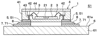
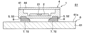
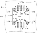
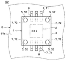
- FIG. 3 is a top layout diagram showing the semiconductor device of the first embodiment. It is sectional drawing which shows the cross section between II-II in FIG. It is sectional drawing which shows the cross section between III-III in FIG.
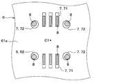
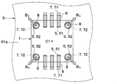
- FIG. 3 is a diagram showing a substrate preparing process in the manufacturing process of the semiconductor device of FIG. 1.
- FIG. 4B is a diagram showing a process of aligning the semiconductor package and the substrate with each other, which is a process following FIG. 4A. It is a figure which shows the surface tension vector by the melted solder in the joining process of the semiconductor package and board
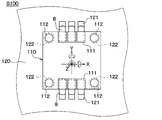
- FIG. 11 is a top view layout diagram showing a conventional semiconductor device.
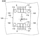
- FIG. 11 is a top view layout diagram showing a conventional semiconductor device.
- FIG. 10 is a diagram showing a state in which a mounting posture of a semiconductor package is broken in a solder joining process in a conventional semiconductor device. It is a figure which shows the mounting attitude of the semiconductor package in the semiconductor device of FIG.
- FIG. 9 is a top layout diagram showing a semiconductor device of a second embodiment. It is a figure which shows the surface tension vector by the melted solder in the process of solder joining among the manufacturing processes of the semiconductor device of FIG.
- FIG. 9 is a top layout diagram showing a semiconductor device of a third embodiment. It is a figure which shows the surface tension vector by the melted solder in the process of solder joining among the manufacturing processes of the semiconductor device of FIG. FIG.
- FIG. 11 is a diagram showing an arrangement relationship between the solder, the signal electrode and the signal land immediately before the solder joining step, which is a region indicated by a chain double-dashed line in FIG. 10.
- FIG. 11B is a diagram showing the wetting and spreading of the melted solder during the solder joining process after the mounting process of the semiconductor package shown in FIG. 11A. It is a top layout view showing a semiconductor device of a fourth embodiment. It is a figure which shows the surface tension vector by the melted solder in the process of solder joining among the manufacturing processes of the semiconductor device of FIG.
- the semiconductor device S1 of the first embodiment will be described with reference to FIGS.
- the semiconductor device S1 of the present embodiment is applied to, for example, an electronic component that is mounted on a vehicle such as an automobile and that includes a physical quantity sensor that outputs a signal according to the physical quantity when a physical quantity such as acceleration or angular velocity is applied.
- the semiconductor device S1 is configured to include an acceleration sensor that outputs a signal according to the acceleration when the acceleration is applied, and is applied to applications such as airbags for vehicle occupant protection devices that require high sensor accuracy.
- it can be applied to other applications.
- FIG. 1 the outline of a semiconductor chip 2 which will be described later, which is not visible in a top view, is indicated by a chain double-dashed line in order to make it easier to see and to help understand the configuration.
- the outline of 72 is shown by a broken line, and the auxiliary electrode 52 is shown by a solid line. Further, in FIG. 1, for the same purpose as above, among the solders 8 described later, those which are hidden by the semiconductor package 1 and are not visible are omitted from the top view.
- the semiconductor device S1 of the present embodiment includes a semiconductor package 1 including an electrode 5 and a substrate 6 including a conductive land 7, and these are electrically connected via a solder 8. It becomes.
- the semiconductor package 1 is substantially parallel to a mounting surface of the substrate 6 facing the semiconductor package 1, that is, one surface 61a, and a signal electrode 51 and a signal land 71, which will be described later in a top view, are aligned. It is configured to be installed in a closed state.
- the mounting state of the semiconductor package 1 described above will be referred to as a “state in which the mounting posture is controlled”.
- the semiconductor package 1 includes, for example, as shown in FIG. 2 or FIG. 3, a semiconductor chip 2 having a sensor section 21, a housing 4 having a recess and an electrode 5 for accommodating the sensor section 21, and a wire electrically connecting them. 3 and 3.
- the semiconductor package 1 has, for example, a structure in which the electrodes 51 and 52 are arranged inside the outer contour of the semiconductor package 1 in a top view, and has a SON structure in the present embodiment.
- the sensor portion 21 of the semiconductor chip 2 is electrically connected to the signal electrode 51 exposed to the outside of the housing 4 via the wire 3, the electrode 42, and the wiring 43. It is connected and outputs the signal of the sensor unit 21 to the outside.
- the semiconductor chip 2 is mainly made of a semiconductor material such as silicon, and is manufactured by a normal semiconductor process. As shown in FIG. 2, when the semiconductor chip 2 is applied with a physical quantity, the semiconductor chip 2 is provided with a sensor section 21 that outputs a signal corresponding to the physical quantity. For example, as shown in FIG. 2, the semiconductor chip 2 is mounted on the bottom surface of the recess of the housing 4 via a die bond material (not shown), and is electrically connected to the electrode 42 in the recess via the wire 3. ing.
- the semiconductor chip 2 including the sensor unit 21 is mounted in the recess of the housing 4 via a die bond material (not shown), and the electrode 42 formed inside the recess is connected via the wire 3 to the electrode 42.
- the semiconductor chip 2 is mounted on a circuit chip made of another silicon substrate on which circuit elements are formed, is connected to the circuit chip by a wire 3, and the circuit chip and the electrode 42 are connected by another wire, The semiconductor chip 2 may be connected to the signal electrode 51.
- the circuit chip is mounted on the bottom surface of the recess of the housing 4 via a die bond material (not shown). As described above, the mounting of the semiconductor chip 2 on the housing 4 and the connection to the signal electrode 51 may be appropriately changed.
- the sensor unit 21 has an arbitrary configuration, for example, when a physical quantity such as acceleration or angular velocity is applied, outputs a signal according to the physical quantity.
- the sensor unit 21 may have a configuration in which a comb-teeth electrode is formed on a movable unit that functions as a weight to detect a change in capacitance, or when a physical quantity is applied using a piezoresistive element. The method of detecting the distortion may be used, and the configuration is arbitrary.
- the semiconductor package 1 functions as an acceleration sensor when the sensor unit 21 outputs a signal corresponding to acceleration, and the angular velocity when the sensor unit 21 outputs a signal corresponding to angular velocity. Functions as a sensor. Further, since the sensor unit 21 may employ a known sensor structure such as an acceleration sensor or an angular velocity sensor, a detailed description of the sensor structure will be omitted in this specification.
- the wire 3 is a connecting member made of a metal material such as gold, and is connected to the semiconductor chip 2 and the electrode 42 of the housing 4 by wire bonding or the like.
- the housing 4 includes a main body portion 41 having a concave portion for accommodating the semiconductor chip 2, an electrode 42 formed in the concave portion, a signal electrode 51 and an auxiliary electrode 52 exposed to the outside, The wiring 43 that electrically connects the electrode 42 and the signal electrode 51 is provided, and the lid portion 44.
- the body 41 is made of ceramics such as alumina.
- the main body 41 has a structure in which a lid 44 made of, for example, a metal material is connected to cover the recess by soldering or the like, and covers the semiconductor chip 2 for protection.
- the electrodes 5 are, as shown in FIG. 2 or FIG. 3, a plurality of signal electrodes 51 for transmitting signals output from the semiconductor chip 2 and a plurality of auxiliary electrodes not used for signal transmission. And the electrode 52.
- the signal electrode 51 and the auxiliary electrode 52 are connected to the conductive land 7 formed on the substrate 6 via the solder 8.
- the signal electrode 51 is arranged in a state where its outer contour is aligned with, for example, a part of the outer contour of the signal land 71 of the substrate 6 shown in FIG. 1, and as shown in FIG. It is electrically connected.
- the signal electrode 51 has, for example, a rectangular plate shape, but its shape is arbitrary.
- a plurality of signal electrodes 51 are provided, and for example, as shown in FIG. 1, they are arranged at a distance from each other on the outer peripheral portion of the main body 41 of the housing 4 when viewed from above.
- auxiliary electrodes 52 are provided, are circular in a plan view, and are arranged one at each of the four corners of the outer contour of the semiconductor package 1.
- the auxiliary electrode 52 is connected to the auxiliary land 72 of the substrate 6 via the solder 8.
- the auxiliary electrode 52 may have an elliptical shape, a polygonal shape, or any other shape as well as a circular shape in a plan view.
- the auxiliary electrode 52 is a dummy electrode used together with the auxiliary land 72 of the substrate 6 to control the mounting posture of the semiconductor package 1 on the substrate 6, and is referred to as an “attitude control electrode”. Can be done.
- the plurality of auxiliary electrodes 52 are arranged symmetrically with respect to the center of the semiconductor package 1 in a plan view together with a plurality of overlapping auxiliary lands 72 described later in order to control the mounting posture of the semiconductor package 1. The reason for this will be described later in the description of the method for manufacturing the semiconductor device S1.
- the substrate 6 includes a base material 61 and lands 7 for mounting the semiconductor package 1, and circuit wirings (not shown) connected to the signal lands 71 of the lands 7 are formed. It is a wiring board. It suffices for the substrate 6 to have a structure capable of mounting the semiconductor package 1, and may have lands for mounting other electronic components (not shown) in addition to the lands 7, and the structure thereof may be appropriately changed. To be done.
- the substrate 6 corresponds to an "object to be mounted” on which the semiconductor package 1 is mounted.
- the mounted object is the substrate 6
- the base material 61 is, for example, as shown in FIG. 2 or 3, a plate shape having one surface 61a, and is made of an arbitrary material such as glass epoxy resin.
- the land 7 is formed on the one surface 61 a of the base material 61.
- the land 7 is made of, for example, a metal material such as copper, and includes a signal land 71 to which the signal electrode 51 is connected via the solder 8 and an auxiliary land 72 to which the auxiliary electrode 52 is connected via the solder 8.
- a plurality of signal lands 71 are provided on one surface 61a of the base material 61, are electrically connected to the signal electrodes 51 of the semiconductor package 1, and are connected to wirings (not shown), and are output from the semiconductor chip 2.
- the signal is transmitted.
- the signal land 71 has, for example, a quadrangular plate shape and is arranged so as to match the position of the signal electrode 51 of the semiconductor package 1.
- the plurality of signal lands 71 are arranged at a distance from each other in a state where their extending directions are aligned in a top view, as shown in FIG. 1, for example, but the present invention is not limited to this. The arrangement and the number are appropriately changed according to the signal electrode 51.
- the auxiliary land 72 is a member that makes a pair with the auxiliary electrode 52 of the semiconductor package 1.
- a plurality of auxiliary lands 72 are provided on one surface 61a of the base material 61 and control the mounting posture of the semiconductor package 1.
- the plurality of auxiliary lands 72 have, for example, a circular shape in a plan view, and are arranged so as to match the positions of the auxiliary electrodes 52 of the semiconductor package 1, that is, symmetrically arranged like the auxiliary electrodes 52.
- the shape of the auxiliary land 72 is not limited to a circular shape in plan view, but may be an elliptical shape, a polygonal shape, or any other shape.
- the planar size of the auxiliary land 72 is larger than that of the auxiliary electrode 52 in order to secure a large amount of solder 8 and improve the joint reliability with the semiconductor package 1.
- the plurality of auxiliary lands 72 are arranged so that the center thereof is offset from the center of the auxiliary electrode 51 in a predetermined direction in order to control the flow of the solder 8 melted when the semiconductor package 1 is mounted. Details of this arrangement and the effect thereof will be described later.
- the auxiliary land 72 is a dummy land used together with the auxiliary electrode 52 of the semiconductor package 1 to control the mounting attitude of the semiconductor package 1, and may be referred to as an “attitude control land”. ..
- the solder 8 is formed on the lands 71 and 72 by printing, for example, and is used for mounting the semiconductor package 1.
- attitude control land and the attitude control electrode connected to the attitude control land via the solder 8 may be referred to as "a pair of attitude control units" for convenience in the following description. That is, the semiconductor device S1 includes a plurality of “a pair of attitude control units”, and these pair of attitude control units are arranged symmetrically with respect to the center of the semiconductor package 1 in a plan view.
- the above is the basic configuration of the semiconductor device S1 of the present embodiment.
- FIG. 4A to 4C although the cross section is not shown, the solder 8 is hatched for easy understanding and understanding.
- the components other than the outer contour of the semiconductor package 1, the electrodes 51 and 52, the substrate 6, the lands 71 and 72, and the solder 8 are omitted for clarity.
- the semiconductor device S1 can adopt any manufacturing process of the semiconductor device except for the control of the mounting posture in the joining process with the solder 8 described later, in the present specification, the process related to the control of the mounting posture will be mainly described. Explained.
- a board 6 having signal lands 71 and auxiliary lands 72 is prepared, and solder 8 is applied onto the lands 71, 72 by printing.
- the substrate 6 is provided with four circular auxiliary lands 72 in a plan view and is symmetrically arranged.
- the four auxiliary lands 72 are arranged in point symmetry with respect to the center C1 between the plurality of auxiliary lands 72, as shown in FIG. 4A.
- the center C1 is the center position between the four auxiliary lands 72 in a plan view, and in the present embodiment, the center position between the four auxiliary electrodes 52 when the semiconductor package 1 is mounted on the substrate 6. It is a part that overlaps with.
- the signal land 71 is applied to one end side where the semiconductor package 1 is mounted. Further, with respect to the auxiliary land 72, in the next step shown in FIG. 4B, the solder 8 is applied to at least a portion located in the inner region of the outer contour of the auxiliary electrode 51, and the remaining portion is exposed from the solder 8. This is to control the mounting posture of the semiconductor package 1 by causing the solder 8 applied to the auxiliary land 72 to flow toward the center C1 when melted in the reflow process.
- solder 8 When applying the solder 8 to the signal land 71 and the auxiliary land 72, it is desirable to apply the solder 8 to the inside of the outer contour of the lands 71 and 72. This is to prevent the solder 8 from protruding from the outer contours of the lands 71 and 72 when the semiconductor package 1 shown in FIG. 4B is mounted and from generating solder balls due to the protruding solder 8 during the reflow process.
- a semiconductor package 1 manufactured by a normal semiconductor process and provided with a signal electrode 51 and an auxiliary electrode 52 is prepared, and the semiconductor package 1 is placed on the substrate 6 while being aligned. ..
- the auxiliary electrode 52 has its center offset from the center of the auxiliary land 72, while the auxiliary electrode 52 is concentrically arranged with the solder 8.
- the semiconductor package 1 is placed on the substrate 6 so that More specifically, at this time, as shown in FIG. 4B, the four auxiliary lands 72 are offset such that the centers of the four auxiliary lands 72 are closer to the center C1 side than the centers of the opposing auxiliary electrodes 52.
- the solder 8 is melted by heating and the semiconductor package 1 and the substrate 6 are joined.
- the molten solder 8 on each auxiliary land 72 flows toward the center C1, and the semiconductor package 1 due to the surface tension of the molten solder 8 is moved to the center C1 as indicated by the white arrow.
- a force B s is drawn to the side.
- the pulling force B s is referred to as “surface tension vector B s ” for convenience of description.
- the surface tension vector B s is generated by the number of the four auxiliary lands 72 that are the attitude control lands in the present embodiment, and as shown by the white arrow in FIG. 4C, all of them are in the state of heading to the center C1.
- the surface tension vector B s is offset as a whole force by pulling each of the four corners of the semiconductor package 1 in the direction of the center C1, and acts to keep the semiconductor package 1 in a predetermined posture.
- the solder 8 applied on the signal land 71 is melted and spread like the solder 8 on the auxiliary land 72, and the outer contour of the signal electrode 51 overlaps the outer contour of the signal land 71.
- the solder 8 on the auxiliary land 72 causes a self-alignment action of preventing the semiconductor package 1 from tilting in an unintended direction, and the solder 8 on the signal land 71 self-aligns with the signal electrode 51.
- offset direction the direction from the center of the auxiliary electrode 52 to the center of the auxiliary land 72 in a straight line in plan view.
- the auxiliary electrode 52 is arranged inside the outer contour of the auxiliary land 72, and at least on the opposite side of the outer contour of the auxiliary electrode 52 to the outer contour of the auxiliary land 72. It is preferable that This is because in the solder joining process, almost all of the melted solder 8 spreads in the offset direction side so as to increase the accuracy of controlling the mounting attitude of the semiconductor package 1.
- the plurality of auxiliary lands 72 have a difference in heat capacity of not more than a predetermined value. This is to prevent the melting timing of the solder 8 on the plurality of auxiliary lands 72 from deviating, that is, reducing the effect of maintaining the mounting posture of the semiconductor package 1 due to the deviation of the generation timing of the surface tension vector B s. Is.
- An example of setting the difference in heat capacities to a predetermined value or less is, for example, making the areas of the auxiliary lands 72 the same or substantially the same, but is not limited to this.
- the solder 8 is re-cured, and the semiconductor package 1 is mounted and fixed on the substrate 6.
- the semiconductor device S1 mounted on the substrate 6 can be manufactured while the semiconductor package 1 maintains a predetermined mounting posture with respect to the one surface 61a which is the mounting surface of the substrate 6.
- auxiliary electrode 52 and the auxiliary land 72 that is, the pair of attitude control units in the present embodiment are arranged in point symmetry. Any symmetric arrangement that balances B s may be used.
- the auxiliary electrode 52 and the auxiliary land 72 may be arranged in line symmetry.
- the left-right direction on the paper surface is the X direction
- the direction orthogonal to the X direction on the paper surface is the Y direction
- the direction orthogonal to the XY plane is the Z direction.
- a part or all of the land 7 that is hidden by the semiconductor packages 1 and 110 and is not visible in a plan view is shown by a broken line
- the electrodes 5, 111 and 112 are shown by solid lines. It shows with.
- a semiconductor package 110 having a signal electrode 111 and an auxiliary electrode 112 is mounted on a substrate 120 having a signal land 121 and an auxiliary land 122 via solder 8.
- the signal land 121 has a plane size larger than that of the signal electrode 111
- the auxiliary land 122 has a plane size larger than that of the auxiliary electrode 112.
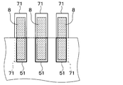
- the signal land 121 and the auxiliary land 122 have a shape in which the electrode 111 or 112 connected via the solder 8 is expanded in the same direction. Even with such a structure, since the amount of the solder 8 is increased, it is possible to secure the joining reliability after the solder joining.
- solder 8 applied on the lands 121 and 122 of the substrate 120 covers a part of the inside of the outer rim of the lands 121 and 122 and exposes the rest. This is to prevent the formation of solder balls or solder bridges due to the molten solder 8 protruding from the lands 121 and 122 when the semiconductor package 1 is mounted.
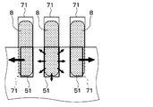
- the molten solder 8 spreads in the same direction on the lands 121 and 122 during solder joining, so that the semiconductor package 110 is in a state in which it is easy to swim until the solder 8 is rehardened. Will end up. If some external force is applied at this time, the semiconductor package 110 is mounted on the substrate 120 in a posture displaced in an unintended direction on the XY plane or the Z direction, as shown in FIG. 5B, for example.
- the semiconductor device S1 of this embodiment is manufactured in a state in which the mounting posture of the semiconductor package 1 is controlled by the surface tension vector as described above. Therefore, as shown in FIG. 6, the semiconductor device S1 has a structure in which the positional displacement between the semiconductor package 1 and the substrate 6 in the X direction, the Y direction, and the Z direction is suppressed.
- the semiconductor device S1 has an improved structure.
- the auxiliary electrode 52 and the auxiliary land 72 cause the surface tension vector B s that pulls the semiconductor package 1 in the predetermined direction by spreading the molten solder 8 in the predetermined direction in the solder joining process. It is arranged so as to be offset. Then, the plurality of auxiliary electrodes 52 and the auxiliary lands 72 are symmetrically arranged so that the surface tension vector B s generated in the solder joining process is in a balanced state, and the area of the auxiliary lands 72 is larger than that of the auxiliary electrodes 52. Therefore, the amount of the solder 8 is set to a predetermined amount or more.
- the mounting posture of the semiconductor package 1 is controlled and the amount of the solder 8 is set to a predetermined amount or more, so that the reliability of the solder joint can be secured, that is, the mounting posture
- the structure ensures both securing and reliability of solder bonding.
- the semiconductor device S1 whose mounting posture is controlled is mounted on a vehicle, for example, it is easier to match the detection axis of the physical quantity of the sensor unit 21 with the traveling direction of the vehicle.
- the structure is highly accurate and is particularly suitable for applications requiring sensor accuracy.
- the mounting posture of the semiconductor package 1 is controlled, the solder 8 melted in the solder joining process is suppressed from protruding outside the outer contour of the land 7, and thus the generation of solder balls and solder bridges is suppressed. The effect is also obtained.
- FIG. 7 as in FIG. 1, the outline of the semiconductor chip 2 which is not visible in a top view is indicated by a chain double-dashed line, and the outline of the signal land 71 hidden by the semiconductor package 1 and the outline of the auxiliary land 72 are indicated by broken lines. , The auxiliary electrode 52 is shown by a solid line. Further, in FIG. 7, for the same purpose as above, the solder 8 that is hidden by the semiconductor package 1 and is not visible in the top view is omitted. Although the cross section is not shown in FIG. 8, in order to make it easier to see and facilitate understanding, the solder 8 is hatched, and the outside of the semiconductor package 1, the electrodes 51 and 52, the substrate 6, the lands 71 and 72 and the solder 8 are excluded. The constituent elements of are omitted.
- the center of the auxiliary land 72 is arranged farther from the center C1 of the plurality of auxiliary electrodes 52 than the center of the auxiliary electrodes 52 facing each other in plan view. This is different from the first embodiment in that In the present embodiment, this difference will be mainly described.
- the semiconductor device S2 of the present embodiment is manufactured by the same manufacturing method as that of the first embodiment, but as shown in FIG. 8, for example, all of the plurality of surface tension vectors B s generated in the solder bonding step are semiconductors. It is configured to face the outside of the package 1.
- the auxiliary land 72 is arranged so as to include the auxiliary electrode 52 in a plan view, and has a shape extending in the radial direction with the center C1 as an axis. Further, in the step of applying the solder 8, the solder 8 is applied to at least a portion of the auxiliary land 72 located in the inner region of the outer contour of the auxiliary electrode 52, and then the semiconductor package 1 is mounted. Then, in the solder joining step, the molten solder 8 wets and spreads in a radial direction with the center C1 as an axis in a plan view, and a plurality of surface tension vectors B s pulling the semiconductor package 1 in the radial direction at the four corners thereof. Occurs.
- these surface tension vectors Bs are in the opposite direction to those of the first embodiment, they are in a state of being balanced as a whole force, and serve to prevent the semiconductor package 1 from tilting in an unintended direction. As a result, the semiconductor package 1 is mounted on the substrate 6 in a state where the mounting posture is controlled.
- the pair of attitude control units are symmetrically arranged as in the first embodiment, and the semiconductor device S2 can obtain the same effect as this.
- a semiconductor device S3 of the third embodiment will be described with reference to FIGS. 9 to 11B.
- FIGS. 9 and 10 the outline of the portion of the signal land 71 hidden in the semiconductor package 1 is shown by a broken line and the signal electrode 51 is shown by a solid line for easy viewing.
- the outer contour of the semiconductor chip 2 is further indicated by a chain double-dashed line.
- 11A and 11B the cross-section is not shown for the sake of clarity, but the solder 8 is hatched and the signal electrode 51 is shown by a thick solid line, and a portion of the signal land 71 that is hidden by the semiconductor package 1 and cannot be seen. Is indicated by a broken line.
- FIGS. 11A and 11B the direction in which the melted solder 8 spreads inside the outer contour of the semiconductor package 1 is indicated by an arrow.
- the semiconductor device S3 of the present embodiment does not have the auxiliary electrode 52 and the auxiliary land 72, and the signal electrode 51 and the signal land 71 are the attitude control electrode and the attitude control land, respectively. This is different from the first embodiment described above. In the present embodiment, this difference will be mainly described.
- the signal electrodes 51 extend so as to intersect the outer contour of the semiconductor package 1, and three signal electrodes 51 are arranged on each of the four sides of the outer contour. .. That is, in this embodiment, the semiconductor package 1 has a QFN structure.
- the plurality of signal electrodes 51 are connected to the signal lands 71 via the solder 8, and are arranged symmetrically with the signal lands 71 connected via the solder 8 in a plan view.
- the three signal electrodes 51 intersecting one side of the contour of the semiconductor package 1 are arranged symmetrically with respect to the central signal electrode 51. ing.
- the above-mentioned arrangement relationship of the plurality of signal electrodes 51 is the same for the other signal electrodes 51 intersecting with the other side forming the outline of the semiconductor package 1. That is, in the semiconductor device S3 of the present embodiment, the signal electrode 51 and the signal land 71 connected to the signal electrode 51 via the solder 8 are a pair of attitude control units, and the plurality of pair of attitude control units are the center of the semiconductor package 1. It is arranged symmetrically with respect to.
- the three signal electrodes 51 shown in FIG. 11A will be mainly described as a representative example.
- the signal electrode 51 at the left end of the paper among the three signal electrodes 51 shown in FIG. 11A is referred to as “left signal electrode 51”, and the central signal electrode 51 is referred to as “middle signal electrode 51”.
- the signal electrode 51 at the right end of the paper is referred to as "right signal electrode 51".
- each of the right signal electrode 51 and the left signal electrode 51 has a middle width in a direction parallel to one side of an outer contour of the semiconductor package 1 (hereinafter, referred to as “outer parallel direction”).
- the shape is smaller than the signal electrode 51 and the signal land 71.
- the right signal electrode 51 and the left signal electrode 51 have the same area and are arranged so as to overlap one side of the opposing signal lands 71 on the side of the middle signal electrode 51 as shown in FIG. 11A.
- the middle signal electrode 51 has the same width as the opposing signal land 71 in the outer contour parallel direction, and the outer contour thereof is arranged to overlap the outer contour of the signal land 71.
- the signal lands 71 are provided in the same number as the signal electrodes 51, and are arranged in a portion corresponding to the signal electrodes 51.
- the plurality of signal lands 71 have at least the same area as the area disposed inside the outer contour of the semiconductor package 1, and as shown in FIG. It is said that.
- the melted solder 8 spreads in the same direction immediately under the middle signal electrode 51 and spreads in the same direction right below the right signal electrode 51 mainly on the right side of the drawing as shown in FIG. 11B.
- the left signal electrode 51 it spreads mainly in the leftward direction on the paper surface. This is the same state on all four sides forming the outer contour of the semiconductor package 1.
- the semiconductor device S3 can obtain the same effect as that of the first embodiment.
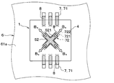
- the cross section is not shown in FIG. 13 for clarity, the solder 8 is hatched, and the direction of the surface tension vector B s generated at the time of joining by the solder 8 is shown by a white arrow.
- the semiconductor device S4 of the present embodiment has only one auxiliary electrode 52 and one auxiliary land 72, and these are an attitude control electrode and an attitude control land. This is different from the first embodiment. In the present embodiment, this difference will be mainly described.
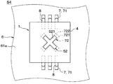
- auxiliary land 72 As shown in FIG. 12, there is only one auxiliary land 72 in this embodiment, and it functions as an attitude control land.
- the auxiliary land 72 has a plurality of extending portions 721 extending in the radial direction with the center of the semiconductor package 1 as an axis in a plan view in a state where the semiconductor package 1 is mounted. Become.
- the extension portion 721 is referred to as a “first extension portion 721” for convenience.
- the first extension portion 721 preferably has the same plane size and the same plane shape as the other first extension portions 721 in order to easily adjust the surface tension vector B s described later.
- the auxiliary electrode 52 is only one in this embodiment, functions as an attitude control electrode, and forms a pair of attitude control units together with the auxiliary land 72.
- the auxiliary electrode 52 is arranged so as to be included inside the outer contour of the auxiliary land 72 in plan view, and extends along the first extending portion 721.
- the plurality of extended second extending portions 521 are provided. That is, when the auxiliary land 72 has the four first extending portions 721, the auxiliary electrode 52 has the four second extending portions 521.
- the second extending portion 521 preferably has the same plane size and the same plane shape as the other second extending portions 521. Moreover, the number of the second extending portions 521 may be the same as the number of the first extending portions 721, and the number is appropriately changed.
- the first extending portion 721 protrudes outside the second extending portion 521 in the extending direction in plan view.
- the auxiliary land 72 has a plurality of outer portions 722, with a portion of the first extended portion 721 outside the outer contour of the opposing second extended portion 521 being the outer portion 722.
- the plurality of outer portions 722 are arranged symmetrically with respect to the center of the semiconductor package 1, for example, line symmetrical or point symmetrical in order to adjust the surface tension vector B s to ensure the mounting posture of the semiconductor package 1. ing.
- the plurality of outer portions 722 are regions where the molten solder 8 spreads when the semiconductor package 1 is joined by the solder 8 as shown in FIG.
- the symmetrical arrangement of the plurality of outer portions 722 causes the surface tension vectors B s generated in the plurality of outer portions 722 to cancel each other, as shown in FIG. 13.
- the semiconductor device S4 has a structure in which the amount of the solder 8 is increased and the semiconductor package 1 is suppressed from unintentional movement during solder joining.
- the pair of attitude control units are arranged near the center of the mounting surface of the semiconductor package 1 and can be used to secure the heat dissipation of the semiconductor package 1 after solder bonding.
- the outer portion 722 has the same or substantially the same plane as the other outer portions 722 when the plurality of first extending portions 721 and the second extending portions 521 have the same or similar plane size and shape. It is preferably sized.
- the attitude control land and the attitude control electrode are arranged such that their centers are offset in a plan view, but in the present embodiment, these centers overlap. It may be arranged.
- the semiconductor package 1 may have a structure that functions as a physical quantity sensor, and the semiconductor chip 2 may be covered with mold resin except the sensor portion 21, or any other structure may be adopted. May be.
- attitude control electrode of the electrode 5 and the attitude control land of the land 7 are symmetrically arranged.
- this symmetrical arrangement does not mean only when the contours of the attitude control electrodes and the attitude control lands are the same when they are rotated with respect to a predetermined point or bent with respect to a predetermined line. ..
- the symmetrical arrangement here also includes, for example, the case where the outer contours of at least the portions where the solder 8 spreads out of the attitude control lands are the same.
- the plurality of attitude control lands are located closer to the outer center of the semiconductor package 1 than the center of the attitude control electrodes whose centers are opposed to each other in plan view, or The example in which it is arranged at a distant position has been described.
- the attitude control electrodes and the attitude control lands have only to be arranged so that a plurality of surface tension vectors B s generated at the time of joining with the solder 8 cancel each other out and balance each other, and the above arrangement and number are limited. It is not something that will be done.
- one posture control electrode and one posture control land are arranged at the four corners of the outer shape of the quadrangular plate-shaped semiconductor package 1, that is, a total of four electrodes and lands are arranged, May be done.
- the center of the attitude control land is closer to the center of the semiconductor package 1 than the center of the attitude control electrode, and the remaining The two may be arranged in the opposite relationship.
- the plurality of surface tension vectors B s cancel and balance each other, so that the semiconductor package 1 is prevented from tilting in an unintended direction.
- the arrangement of the attitude control electrodes and the attitude control lands may be changed as described above, or may be another arrangement in which the surface tension vector B s is balanced, and the numbers thereof are also appropriately changed. May be.
- attitude control electrodes and the attitude control lands may be the same number and symmetrically arranged in the above meaning, and are not limited to the numbers described in the above embodiments.
- the land 7 for mounting the semiconductor package 1 may be used and may not necessarily be the substrate.
Landscapes
- Engineering & Computer Science (AREA)
- Microelectronics & Electronic Packaging (AREA)
- Physics & Mathematics (AREA)
- Condensed Matter Physics & Semiconductors (AREA)
- General Physics & Mathematics (AREA)
- Computer Hardware Design (AREA)
- Power Engineering (AREA)
- Manufacturing & Machinery (AREA)
- Geometry (AREA)
- Wire Bonding (AREA)
- Electric Connection Of Electric Components To Printed Circuits (AREA)
Priority Applications (3)
| Application Number | Priority Date | Filing Date | Title |
|---|---|---|---|
| CN201980088486.XA CN113287373B (zh) | 2019-01-10 | 2019-12-19 | 半导体装置及其制造方法 |
| DE112019006628.5T DE112019006628T5 (de) | 2019-01-10 | 2019-12-19 | Halbleitervorrichtung und herstellungsverfahren dafür |
| US17/370,770 US20210335700A1 (en) | 2019-01-10 | 2021-07-08 | Semiconductor device and production method thereof |
Applications Claiming Priority (2)
| Application Number | Priority Date | Filing Date | Title |
|---|---|---|---|
| JP2019002913A JP7167721B2 (ja) | 2019-01-10 | 2019-01-10 | 半導体装置およびその製造方法 |
| JP2019-002913 | 2019-01-10 |
Related Child Applications (1)
| Application Number | Title | Priority Date | Filing Date |
|---|---|---|---|
| US17/370,770 Continuation US20210335700A1 (en) | 2019-01-10 | 2021-07-08 | Semiconductor device and production method thereof |
Publications (1)
| Publication Number | Publication Date |
|---|---|
| WO2020145076A1 true WO2020145076A1 (ja) | 2020-07-16 |
Family
ID=71521501
Family Applications (1)
| Application Number | Title | Priority Date | Filing Date |
|---|---|---|---|
| PCT/JP2019/049879 WO2020145076A1 (ja) | 2019-01-10 | 2019-12-19 | 半導体装置およびその製造方法 |
Country Status (5)
| Country | Link |
|---|---|
| US (1) | US20210335700A1 (zh) |
| JP (1) | JP7167721B2 (zh) |
| CN (1) | CN113287373B (zh) |
| DE (1) | DE112019006628T5 (zh) |
| WO (1) | WO2020145076A1 (zh) |
Citations (3)
| Publication number | Priority date | Publication date | Assignee | Title |
|---|---|---|---|---|
| JP2001156432A (ja) * | 1999-11-29 | 2001-06-08 | Opnext Japan Inc | モジュール及び電子部品の実装方法 |
| WO2009081929A1 (ja) * | 2007-12-26 | 2009-07-02 | Fujikura Ltd. | 実装基板及びその製造方法 |
| JP2018500752A (ja) * | 2014-12-19 | 2018-01-11 | ウォーカー マイロンWALKER, Myron | 集積回路パッケージのはんだ付け性及び自己整合性を改良するスポーク付きはんだパッド |
Family Cites Families (20)
| Publication number | Priority date | Publication date | Assignee | Title |
|---|---|---|---|---|
| JPH1117319A (ja) * | 1997-06-26 | 1999-01-22 | Matsushita Electric Ind Co Ltd | チップの実装方法 |
| JP2001196731A (ja) * | 2000-01-13 | 2001-07-19 | Sony Corp | バンプ形成方法および半導体チップの接合方法 |
| JP3656543B2 (ja) * | 2000-10-25 | 2005-06-08 | 松下電器産業株式会社 | 電子部品実装方法 |
| JP2002223062A (ja) * | 2001-01-26 | 2002-08-09 | Toyo Commun Equip Co Ltd | プリント配線基板のパッド形状 |
| JP4637380B2 (ja) * | 2001-02-08 | 2011-02-23 | ルネサスエレクトロニクス株式会社 | 半導体装置 |
| JP2002350244A (ja) * | 2001-05-25 | 2002-12-04 | Hitachi Cable Ltd | ニオイ検知式熱監視システム |
| JP3850755B2 (ja) * | 2002-05-29 | 2006-11-29 | シャープ株式会社 | 半導体装置およびその製造方法 |
| JP4618298B2 (ja) * | 2005-03-29 | 2011-01-26 | 株式会社村田製作所 | 電子部品の実装構造 |
| JP2007043134A (ja) * | 2005-07-05 | 2007-02-15 | Oki Electric Ind Co Ltd | 半導体チップパッケージ及びその製造方法 |
| JP4807199B2 (ja) * | 2006-09-13 | 2011-11-02 | 株式会社デンソー | 湿度センサ装置 |
| JP2011193109A (ja) * | 2010-03-12 | 2011-09-29 | Seiko Epson Corp | 電子デバイス |
| JP5853525B2 (ja) * | 2011-09-16 | 2016-02-09 | 富士電機株式会社 | 半導体チップの位置決め治具及び半導体装置の製造方法 |
| JP5991915B2 (ja) * | 2012-12-27 | 2016-09-14 | ルネサスエレクトロニクス株式会社 | 半導体装置の製造方法 |
| JP2014236187A (ja) * | 2013-06-05 | 2014-12-15 | イビデン株式会社 | 配線板及びその製造方法 |
| JP2015015362A (ja) * | 2013-07-04 | 2015-01-22 | ルネサスエレクトロニクス株式会社 | 半導体装置の製造方法 |
| JP6522980B2 (ja) * | 2015-02-18 | 2019-05-29 | ルネサスエレクトロニクス株式会社 | 半導体装置およびその製造方法 |
| JP5992078B2 (ja) * | 2015-08-03 | 2016-09-14 | ルネサスエレクトロニクス株式会社 | 半導体装置 |
| JP2018056234A (ja) * | 2016-09-27 | 2018-04-05 | キヤノン株式会社 | プリント回路板、電子機器及びプリント回路板の製造方法 |
| JP6956552B2 (ja) * | 2017-07-19 | 2021-11-02 | 株式会社小糸製作所 | 車載用電子回路実装基板 |
| JP7298304B2 (ja) | 2019-05-29 | 2023-06-27 | スズキ株式会社 | 車両用加飾部材固定構造 |
-
2019
- 2019-01-10 JP JP2019002913A patent/JP7167721B2/ja active Active
- 2019-12-19 DE DE112019006628.5T patent/DE112019006628T5/de active Pending
- 2019-12-19 CN CN201980088486.XA patent/CN113287373B/zh active Active
- 2019-12-19 WO PCT/JP2019/049879 patent/WO2020145076A1/ja active Application Filing
-
2021
- 2021-07-08 US US17/370,770 patent/US20210335700A1/en active Pending
Patent Citations (3)
| Publication number | Priority date | Publication date | Assignee | Title |
|---|---|---|---|---|
| JP2001156432A (ja) * | 1999-11-29 | 2001-06-08 | Opnext Japan Inc | モジュール及び電子部品の実装方法 |
| WO2009081929A1 (ja) * | 2007-12-26 | 2009-07-02 | Fujikura Ltd. | 実装基板及びその製造方法 |
| JP2018500752A (ja) * | 2014-12-19 | 2018-01-11 | ウォーカー マイロンWALKER, Myron | 集積回路パッケージのはんだ付け性及び自己整合性を改良するスポーク付きはんだパッド |
Also Published As
| Publication number | Publication date |
|---|---|
| JP7167721B2 (ja) | 2022-11-09 |
| CN113287373A (zh) | 2021-08-20 |
| US20210335700A1 (en) | 2021-10-28 |
| DE112019006628T5 (de) | 2021-09-23 |
| CN113287373B (zh) | 2024-06-21 |
| JP2020113626A (ja) | 2020-07-27 |
Similar Documents
| Publication | Publication Date | Title |
|---|---|---|
| KR100386995B1 (ko) | 반도체 장치 및 그 배선 방법 | |
| TWI479630B (zh) | 具中心接觸件之增強堆疊微電子總成以及其之系統、模組及配置 | |
| US20060049495A1 (en) | Semiconductor package and laminated semiconductor package | |
| US20140284731A1 (en) | Semiconductor device | |
| US20060012038A1 (en) | Semiconductor device, semiconductor device module and method of manufacturing the semiconductor device | |
| US9474180B2 (en) | Method of manufacturing electronic device and electronic device | |
| JP2011039040A (ja) | 垂直にセンサ組み立てる方法 | |
| US7553164B2 (en) | Circuit device and method of manufacturing the same | |
| US9964560B2 (en) | Transfer mold type sensor device | |
| US20090241670A1 (en) | Semiconductor acceleration sensor | |
| JP2004172322A (ja) | 半導体パッケージ及び積層型半導体パッケージ | |
| US7038321B1 (en) | Method of attaching a flip chip device and circuit assembly formed thereby | |
| US7982460B2 (en) | Magnetic sensor module | |
| US6410366B1 (en) | Semiconductor device and manufacturing method thereof, circuit board and electronic equipment | |
| JP2007005452A (ja) | 半導体装置 | |
| WO2020145076A1 (ja) | 半導体装置およびその製造方法 | |
| US20050167817A1 (en) | Microelectronic adaptors, assemblies and methods | |
| JP6773096B2 (ja) | プリント回路板上のmems取り付けにおける振動の縮小 | |
| WO2014203554A1 (ja) | 樹脂封止型センサ装置 | |
| JP7283407B2 (ja) | 電子装置 | |
| JP4952365B2 (ja) | 両面実装回路基板に対する電子部品の実装構造、半導体装置、及び両面実装半導体装置の製造方法 | |
| JPH01145630A (ja) | 液晶表示素子 | |
| WO2021261013A1 (ja) | 電子制御装置および電子制御装置の製造方法 | |
| US20220317147A1 (en) | Electronic device | |
| TW201537674A (zh) | 晶片封裝體及其製造方法 |
Legal Events
| Date | Code | Title | Description |
|---|---|---|---|
| 121 | Ep: the epo has been informed by wipo that ep was designated in this application |
Ref document number: 19908925 Country of ref document: EP Kind code of ref document: A1 |
|
| 122 | Ep: pct application non-entry in european phase |
Ref document number: 19908925 Country of ref document: EP Kind code of ref document: A1 |

