WO2020145076A1 - 半導体装置およびその製造方法 - Google Patents
半導体装置およびその製造方法 Download PDFInfo
- Publication number
- WO2020145076A1 WO2020145076A1 PCT/JP2019/049879 JP2019049879W WO2020145076A1 WO 2020145076 A1 WO2020145076 A1 WO 2020145076A1 JP 2019049879 W JP2019049879 W JP 2019049879W WO 2020145076 A1 WO2020145076 A1 WO 2020145076A1
- Authority
- WO
- WIPO (PCT)
- Prior art keywords
- attitude control
- semiconductor package
- land
- solder
- lands
- Prior art date
Links
Images


Classifications
-
- H—ELECTRICITY
- H05—ELECTRIC TECHNIQUES NOT OTHERWISE PROVIDED FOR
- H05K—PRINTED CIRCUITS; CASINGS OR CONSTRUCTIONAL DETAILS OF ELECTRIC APPARATUS; MANUFACTURE OF ASSEMBLAGES OF ELECTRICAL COMPONENTS
- H05K1/00—Printed circuits
- H05K1/02—Details
- H05K1/11—Printed elements for providing electric connections to or between printed circuits
- H05K1/111—Pads for surface mounting, e.g. lay-out
-
- H—ELECTRICITY
- H01—ELECTRIC ELEMENTS
- H01L—SEMICONDUCTOR DEVICES NOT COVERED BY CLASS H10
- H01L23/00—Details of semiconductor or other solid state devices
- H01L23/48—Arrangements for conducting electric current to or from the solid state body in operation, e.g. leads, terminal arrangements ; Selection of materials therefor
- H01L23/488—Arrangements for conducting electric current to or from the solid state body in operation, e.g. leads, terminal arrangements ; Selection of materials therefor consisting of soldered or bonded constructions
- H01L23/498—Leads, i.e. metallisations or lead-frames on insulating substrates, e.g. chip carriers
- H01L23/49838—Geometry or layout
-
- H—ELECTRICITY
- H01—ELECTRIC ELEMENTS
- H01L—SEMICONDUCTOR DEVICES NOT COVERED BY CLASS H10
- H01L21/00—Processes or apparatus adapted for the manufacture or treatment of semiconductor or solid state devices or of parts thereof
- H01L21/02—Manufacture or treatment of semiconductor devices or of parts thereof
- H01L21/04—Manufacture or treatment of semiconductor devices or of parts thereof the devices having at least one potential-jump barrier or surface barrier, e.g. PN junction, depletion layer or carrier concentration layer
- H01L21/50—Assembly of semiconductor devices using processes or apparatus not provided for in a single one of the subgroups H01L21/06 - H01L21/326, e.g. sealing of a cap to a base of a container
- H01L21/60—Attaching or detaching leads or other conductive members, to be used for carrying current to or from the device in operation
-
- H—ELECTRICITY
- H01—ELECTRIC ELEMENTS
- H01L—SEMICONDUCTOR DEVICES NOT COVERED BY CLASS H10
- H01L23/00—Details of semiconductor or other solid state devices
- H01L23/48—Arrangements for conducting electric current to or from the solid state body in operation, e.g. leads, terminal arrangements ; Selection of materials therefor
- H01L23/488—Arrangements for conducting electric current to or from the solid state body in operation, e.g. leads, terminal arrangements ; Selection of materials therefor consisting of soldered or bonded constructions
- H01L23/498—Leads, i.e. metallisations or lead-frames on insulating substrates, e.g. chip carriers
- H01L23/49811—Additional leads joined to the metallisation on the insulating substrate, e.g. pins, bumps, wires, flat leads
-
- H—ELECTRICITY
- H05—ELECTRIC TECHNIQUES NOT OTHERWISE PROVIDED FOR
- H05K—PRINTED CIRCUITS; CASINGS OR CONSTRUCTIONAL DETAILS OF ELECTRIC APPARATUS; MANUFACTURE OF ASSEMBLAGES OF ELECTRICAL COMPONENTS
- H05K3/00—Apparatus or processes for manufacturing printed circuits
- H05K3/30—Assembling printed circuits with electric components, e.g. with resistor
- H05K3/32—Assembling printed circuits with electric components, e.g. with resistor electrically connecting electric components or wires to printed circuits
- H05K3/34—Assembling printed circuits with electric components, e.g. with resistor electrically connecting electric components or wires to printed circuits by soldering
- H05K3/341—Surface mounted components
- H05K3/3431—Leadless components
- H05K3/3442—Leadless components having edge contacts, e.g. leadless chip capacitors, chip carriers
-
- H—ELECTRICITY
- H01—ELECTRIC ELEMENTS
- H01L—SEMICONDUCTOR DEVICES NOT COVERED BY CLASS H10
- H01L21/00—Processes or apparatus adapted for the manufacture or treatment of semiconductor or solid state devices or of parts thereof
- H01L21/02—Manufacture or treatment of semiconductor devices or of parts thereof
- H01L21/04—Manufacture or treatment of semiconductor devices or of parts thereof the devices having at least one potential-jump barrier or surface barrier, e.g. PN junction, depletion layer or carrier concentration layer
- H01L21/50—Assembly of semiconductor devices using processes or apparatus not provided for in a single one of the subgroups H01L21/06 - H01L21/326, e.g. sealing of a cap to a base of a container
- H01L21/60—Attaching or detaching leads or other conductive members, to be used for carrying current to or from the device in operation
- H01L2021/60007—Attaching or detaching leads or other conductive members, to be used for carrying current to or from the device in operation involving a soldering or an alloying process
-
- H—ELECTRICITY
- H01—ELECTRIC ELEMENTS
- H01L—SEMICONDUCTOR DEVICES NOT COVERED BY CLASS H10
- H01L2224/00—Indexing scheme for arrangements for connecting or disconnecting semiconductor or solid-state bodies and methods related thereto as covered by H01L24/00
- H01L2224/01—Means for bonding being attached to, or being formed on, the surface to be connected, e.g. chip-to-package, die-attach, "first-level" interconnects; Manufacturing methods related thereto
- H01L2224/42—Wire connectors; Manufacturing methods related thereto
- H01L2224/47—Structure, shape, material or disposition of the wire connectors after the connecting process
- H01L2224/48—Structure, shape, material or disposition of the wire connectors after the connecting process of an individual wire connector
- H01L2224/4805—Shape
- H01L2224/4809—Loop shape
- H01L2224/48091—Arched
-
- H—ELECTRICITY
- H05—ELECTRIC TECHNIQUES NOT OTHERWISE PROVIDED FOR
- H05K—PRINTED CIRCUITS; CASINGS OR CONSTRUCTIONAL DETAILS OF ELECTRIC APPARATUS; MANUFACTURE OF ASSEMBLAGES OF ELECTRICAL COMPONENTS
- H05K2201/00—Indexing scheme relating to printed circuits covered by H05K1/00
- H05K2201/09—Shape and layout
- H05K2201/09209—Shape and layout details of conductors
- H05K2201/09372—Pads and lands
- H05K2201/094—Array of pads or lands differing from one another, e.g. in size, pitch, thickness; Using different connections on the pads
-
- H—ELECTRICITY
- H05—ELECTRIC TECHNIQUES NOT OTHERWISE PROVIDED FOR
- H05K—PRINTED CIRCUITS; CASINGS OR CONSTRUCTIONAL DETAILS OF ELECTRIC APPARATUS; MANUFACTURE OF ASSEMBLAGES OF ELECTRICAL COMPONENTS
- H05K2201/00—Indexing scheme relating to printed circuits covered by H05K1/00
- H05K2201/09—Shape and layout
- H05K2201/09209—Shape and layout details of conductors
- H05K2201/09654—Shape and layout details of conductors covering at least two types of conductors provided for in H05K2201/09218 - H05K2201/095
- H05K2201/09781—Dummy conductors, i.e. not used for normal transport of current; Dummy electrodes of components
-
- H—ELECTRICITY
- H05—ELECTRIC TECHNIQUES NOT OTHERWISE PROVIDED FOR
- H05K—PRINTED CIRCUITS; CASINGS OR CONSTRUCTIONAL DETAILS OF ELECTRIC APPARATUS; MANUFACTURE OF ASSEMBLAGES OF ELECTRICAL COMPONENTS
- H05K2201/00—Indexing scheme relating to printed circuits covered by H05K1/00
- H05K2201/10—Details of components or other objects attached to or integrated in a printed circuit board
- H05K2201/10613—Details of electrical connections of non-printed components, e.g. special leads
- H05K2201/10621—Components characterised by their electrical contacts
- H05K2201/10727—Leadless chip carrier [LCC], e.g. chip-modules for cards
-
- H—ELECTRICITY
- H05—ELECTRIC TECHNIQUES NOT OTHERWISE PROVIDED FOR
- H05K—PRINTED CIRCUITS; CASINGS OR CONSTRUCTIONAL DETAILS OF ELECTRIC APPARATUS; MANUFACTURE OF ASSEMBLAGES OF ELECTRICAL COMPONENTS
- H05K2203/00—Indexing scheme relating to apparatus or processes for manufacturing printed circuits covered by H05K3/00
- H05K2203/04—Soldering or other types of metallurgic bonding
- H05K2203/048—Self-alignment during soldering; Terminals, pads or shape of solder adapted therefor
-
- H—ELECTRICITY
- H05—ELECTRIC TECHNIQUES NOT OTHERWISE PROVIDED FOR
- H05K—PRINTED CIRCUITS; CASINGS OR CONSTRUCTIONAL DETAILS OF ELECTRIC APPARATUS; MANUFACTURE OF ASSEMBLAGES OF ELECTRICAL COMPONENTS
- H05K3/00—Apparatus or processes for manufacturing printed circuits
- H05K3/30—Assembling printed circuits with electric components, e.g. with resistor
- H05K3/32—Assembling printed circuits with electric components, e.g. with resistor electrically connecting electric components or wires to printed circuits
- H05K3/34—Assembling printed circuits with electric components, e.g. with resistor electrically connecting electric components or wires to printed circuits by soldering
- H05K3/341—Surface mounted components
- H05K3/3431—Leadless components
- H05K3/3436—Leadless components having an array of bottom contacts, e.g. pad grid array or ball grid array components
-
- Y—GENERAL TAGGING OF NEW TECHNOLOGICAL DEVELOPMENTS; GENERAL TAGGING OF CROSS-SECTIONAL TECHNOLOGIES SPANNING OVER SEVERAL SECTIONS OF THE IPC; TECHNICAL SUBJECTS COVERED BY FORMER USPC CROSS-REFERENCE ART COLLECTIONS [XRACs] AND DIGESTS
- Y02—TECHNOLOGIES OR APPLICATIONS FOR MITIGATION OR ADAPTATION AGAINST CLIMATE CHANGE
- Y02P—CLIMATE CHANGE MITIGATION TECHNOLOGIES IN THE PRODUCTION OR PROCESSING OF GOODS
- Y02P70/00—Climate change mitigation technologies in the production process for final industrial or consumer products
- Y02P70/50—Manufacturing or production processes characterised by the final manufactured product
Definitions
- the present disclosure relates to a semiconductor device having a structure in which a semiconductor package including a plurality of electrodes is mounted via solder, and a manufacturing method thereof.
- the semiconductor package is mounted such that its electrodes are displaced from the land positions of the printed board. It may be done. In such a case, the semiconductor package is connected to the printed circuit board at a position different from the expected position, which may cause a malfunction of the semiconductor device.
- solder joints As a method for ensuring the reliability of solder joints, it is conceivable to increase the amount of solder used for joining and relieve the stress by the solder.
- this method when the semiconductor package is mounted on the substrate, for example, when the solder protrudes from the land and a part of the solder separates, a solder ball is generated, and other electrical problems may occur. Further, according to this method, the movement of the semiconductor package becomes large until the solder is melted and re-cured, and the posture after the semiconductor package is mounted on the substrate (hereinafter referred to as “mounting posture”) shifts.
- the mounting attitude is displaced as used herein means that the semiconductor package is inclined with respect to the surface of the mounted object such as a substrate on which the semiconductor package is mounted, and that the electrode and the mounted object are different from each other. It means that at least one of the positional shifts occurs.
- Such a deviation in the mounting posture of the semiconductor package causes a decrease in sensor accuracy when configuring a semiconductor device including a sensor unit that outputs a signal corresponding to a predetermined physical quantity such as acceleration or angular velocity when applied. It causes a problem and causes a problem.
- a semiconductor device is configured using a semiconductor package having a QFN structure or the like and the printed circuit board described in Patent Document 1, it is possible to suppress the positional deviation between the electrode and the land by self-alignment, but it is not possible to deal with the deviation of the mounting posture. ..
- the present disclosure provides a semiconductor device in which a semiconductor package including a plurality of electrodes is mounted via solder, and can ensure both a mounting posture of the semiconductor package and reliability of solder bonding, and a manufacturing method thereof. To aim.
- the semiconductor device includes a semiconductor package including a plurality of electrodes, a plurality of lands, and a mounted object on which the semiconductor package is mounted.
- the plurality of electrodes are connected to the plurality of lands through the solder, and at least a part of the electrodes of the plurality of electrodes is a mounting surface facing the semiconductor package of the mounted object.
- an attitude control electrode used to control the attitude of the semiconductor package with respect to
- at least some of the lands are attitude control lands used to control the attitude of the semiconductor package with respect to the mounting surface.
- the attitude control electrode overlaps with the attitude control land, and the center of the attitude control electrode is arranged so as to be offset from the center of the attitude control land connected through solder in plan view.
- a plurality of control lands and attitude control electrodes are provided, and the attitude control lands and the attitude control electrodes connected to the attitude control lands through solder are used as a pair of attitude control units to form a pair of attitude control electrodes.
- the parts are arranged symmetrically with respect to the center of the semiconductor package in a plan view.
- the semiconductor package is mounted on the board, and a plurality of pair of posture control units each including the posture control electrodes and the posture control lands connected to the electrodes through the solder are provided.
- the structure is symmetrically arranged with respect to the center of the semiconductor package.
- the pair of attitude control parts are parts where a force resulting from the surface tension of the melted solder, that is, a surface tension vector, is generated by the molten solder spreading when it is connected via the solder.
- a semiconductor device includes a semiconductor package including a plurality of electrodes, an object to be mounted on which the semiconductor package is mounted, including a plurality of lands, and the semiconductor package includes a plurality of electrodes.
- the semiconductor package includes a plurality of electrodes.
- one electrode of the plurality of electrodes is an attitude control electrode used for controlling the attitude of the semiconductor package with respect to the mounting surface of the mounted object facing the semiconductor package.
- One of the plurality of lands is an attitude control land used to control the attitude of the semiconductor package with respect to the mounting surface, and the attitude control land has a plane size larger than that of the attitude control electrode.
- the attitude control electrode in plan view, and has a plurality of extending portions extending in the radial direction with the center of the semiconductor package as an axis. The portions are extended along different directions in the radial direction, and the attitude control electrode is extended along the first extended portion, with the plurality of extended portions serving as the first extended portions.
- a plurality of second extending portions, and a portion outside the outer contour of the facing second extending portion of the first extending portions in plan view is an outer portion, and the outer portion is a semiconductor package.
- the semiconductor device according to the first aspect even in a semiconductor device having only one attitude control electrode and one attitude control land, as in the semiconductor device according to the first aspect, the amount of solder can be secured while soldering is performed.
- the surface tension vector is offset. Therefore, also in the semiconductor device according to the second aspect, the same effect as that of the semiconductor device according to the first aspect can be obtained.
- a method for manufacturing a semiconductor device is a method for manufacturing a semiconductor device in which a semiconductor package including a plurality of electrodes and an object to be mounted including a plurality of lands are connected via solder. Includes preparing a package, preparing an object to be mounted, applying solder on a land of the object to be mounted, and mounting a semiconductor package on the object to be solder-coated. .. In such a configuration, in preparing the semiconductor package, at least two or more electrodes of the plurality of electrodes are used for attitude control for controlling the attitude of the semiconductor package with respect to the mounting surface of the mounted object facing the semiconductor package.
- attitude control lands for controlling the attitude of the semiconductor package with respect to the mounting surface
- solder is applied.
- the attitude control electrode and the attitude control land are arranged with their centers offset from each other.
- the molten solder is wetted and spread from the region inside the posture control land to the region outside the contour of the posture control land in plan view.
- the surface tension vector is the tensile direction of the semiconductor package due to the surface tension of the melted solder in this wetting and spreading, and the entire surface tension vector of the solder applied on each attitude control electrode is in a balanced state.
- a plurality of surface tension vectors are generated when the plurality of attitude control electrodes of the semiconductor package and the plurality of attitude control lands of the board are joined via solder. ..
- the attitude control electrode and the attitude control land are arranged so that their centers are offset from each other, and part of the attitude control land is exposed from the solder.
- the melted solder will wet and spread on the exposed portion.
- the tensile direction of the semiconductor package due to the surface tension of the melted solder in the wetting and spreading is used as a surface tension vector, and the entire surface tension vector of the solder applied on each attitude control electrode is balanced. Therefore, it is possible to suppress unintended movement of the semiconductor package between melting the solder and re-hardening the solder, and manufacturing the semiconductor device configured to be mounted on the substrate while the attitude of the semiconductor package is controlled. can do.
- FIG. 3 is a top layout diagram showing the semiconductor device of the first embodiment. It is sectional drawing which shows the cross section between II-II in FIG. It is sectional drawing which shows the cross section between III-III in FIG.
- FIG. 3 is a diagram showing a substrate preparing process in the manufacturing process of the semiconductor device of FIG. 1.
- FIG. 4B is a diagram showing a process of aligning the semiconductor package and the substrate with each other, which is a process following FIG. 4A. It is a figure which shows the surface tension vector by the melted solder in the joining process of the semiconductor package and board
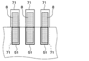
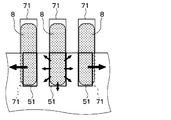
- FIG. 11 is a top view layout diagram showing a conventional semiconductor device.
- FIG. 11 is a top view layout diagram showing a conventional semiconductor device.
- FIG. 10 is a diagram showing a state in which a mounting posture of a semiconductor package is broken in a solder joining process in a conventional semiconductor device. It is a figure which shows the mounting attitude of the semiconductor package in the semiconductor device of FIG.
- FIG. 9 is a top layout diagram showing a semiconductor device of a second embodiment. It is a figure which shows the surface tension vector by the melted solder in the process of solder joining among the manufacturing processes of the semiconductor device of FIG.
- FIG. 9 is a top layout diagram showing a semiconductor device of a third embodiment. It is a figure which shows the surface tension vector by the melted solder in the process of solder joining among the manufacturing processes of the semiconductor device of FIG. FIG.
- FIG. 11 is a diagram showing an arrangement relationship between the solder, the signal electrode and the signal land immediately before the solder joining step, which is a region indicated by a chain double-dashed line in FIG. 10.
- FIG. 11B is a diagram showing the wetting and spreading of the melted solder during the solder joining process after the mounting process of the semiconductor package shown in FIG. 11A. It is a top layout view showing a semiconductor device of a fourth embodiment. It is a figure which shows the surface tension vector by the melted solder in the process of solder joining among the manufacturing processes of the semiconductor device of FIG.
- the semiconductor device S1 of the first embodiment will be described with reference to FIGS.
- the semiconductor device S1 of the present embodiment is applied to, for example, an electronic component that is mounted on a vehicle such as an automobile and that includes a physical quantity sensor that outputs a signal according to the physical quantity when a physical quantity such as acceleration or angular velocity is applied.
- the semiconductor device S1 is configured to include an acceleration sensor that outputs a signal according to the acceleration when the acceleration is applied, and is applied to applications such as airbags for vehicle occupant protection devices that require high sensor accuracy.
- it can be applied to other applications.
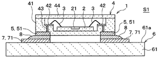
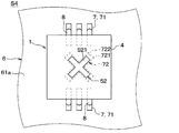
- FIG. 1 the outline of a semiconductor chip 2 which will be described later, which is not visible in a top view, is indicated by a chain double-dashed line in order to make it easier to see and to help understand the configuration.
- the outline of 72 is shown by a broken line, and the auxiliary electrode 52 is shown by a solid line. Further, in FIG. 1, for the same purpose as above, among the solders 8 described later, those which are hidden by the semiconductor package 1 and are not visible are omitted from the top view.
- the semiconductor device S1 of the present embodiment includes a semiconductor package 1 including an electrode 5 and a substrate 6 including a conductive land 7, and these are electrically connected via a solder 8. It becomes.
- the semiconductor package 1 is substantially parallel to a mounting surface of the substrate 6 facing the semiconductor package 1, that is, one surface 61a, and a signal electrode 51 and a signal land 71, which will be described later in a top view, are aligned. It is configured to be installed in a closed state.
- the mounting state of the semiconductor package 1 described above will be referred to as a “state in which the mounting posture is controlled”.
- the semiconductor package 1 includes, for example, as shown in FIG. 2 or FIG. 3, a semiconductor chip 2 having a sensor section 21, a housing 4 having a recess and an electrode 5 for accommodating the sensor section 21, and a wire electrically connecting them. 3 and 3.
- the semiconductor package 1 has, for example, a structure in which the electrodes 51 and 52 are arranged inside the outer contour of the semiconductor package 1 in a top view, and has a SON structure in the present embodiment.
- the sensor portion 21 of the semiconductor chip 2 is electrically connected to the signal electrode 51 exposed to the outside of the housing 4 via the wire 3, the electrode 42, and the wiring 43. It is connected and outputs the signal of the sensor unit 21 to the outside.
- the semiconductor chip 2 is mainly made of a semiconductor material such as silicon, and is manufactured by a normal semiconductor process. As shown in FIG. 2, when the semiconductor chip 2 is applied with a physical quantity, the semiconductor chip 2 is provided with a sensor section 21 that outputs a signal corresponding to the physical quantity. For example, as shown in FIG. 2, the semiconductor chip 2 is mounted on the bottom surface of the recess of the housing 4 via a die bond material (not shown), and is electrically connected to the electrode 42 in the recess via the wire 3. ing.
- the semiconductor chip 2 including the sensor unit 21 is mounted in the recess of the housing 4 via a die bond material (not shown), and the electrode 42 formed inside the recess is connected via the wire 3 to the electrode 42.
- the semiconductor chip 2 is mounted on a circuit chip made of another silicon substrate on which circuit elements are formed, is connected to the circuit chip by a wire 3, and the circuit chip and the electrode 42 are connected by another wire, The semiconductor chip 2 may be connected to the signal electrode 51.
- the circuit chip is mounted on the bottom surface of the recess of the housing 4 via a die bond material (not shown). As described above, the mounting of the semiconductor chip 2 on the housing 4 and the connection to the signal electrode 51 may be appropriately changed.
- the sensor unit 21 has an arbitrary configuration, for example, when a physical quantity such as acceleration or angular velocity is applied, outputs a signal according to the physical quantity.
- the sensor unit 21 may have a configuration in which a comb-teeth electrode is formed on a movable unit that functions as a weight to detect a change in capacitance, or when a physical quantity is applied using a piezoresistive element. The method of detecting the distortion may be used, and the configuration is arbitrary.
- the semiconductor package 1 functions as an acceleration sensor when the sensor unit 21 outputs a signal corresponding to acceleration, and the angular velocity when the sensor unit 21 outputs a signal corresponding to angular velocity. Functions as a sensor. Further, since the sensor unit 21 may employ a known sensor structure such as an acceleration sensor or an angular velocity sensor, a detailed description of the sensor structure will be omitted in this specification.
- the wire 3 is a connecting member made of a metal material such as gold, and is connected to the semiconductor chip 2 and the electrode 42 of the housing 4 by wire bonding or the like.
- the housing 4 includes a main body portion 41 having a concave portion for accommodating the semiconductor chip 2, an electrode 42 formed in the concave portion, a signal electrode 51 and an auxiliary electrode 52 exposed to the outside, The wiring 43 that electrically connects the electrode 42 and the signal electrode 51 is provided, and the lid portion 44.
- the body 41 is made of ceramics such as alumina.
- the main body 41 has a structure in which a lid 44 made of, for example, a metal material is connected to cover the recess by soldering or the like, and covers the semiconductor chip 2 for protection.
- the electrodes 5 are, as shown in FIG. 2 or FIG. 3, a plurality of signal electrodes 51 for transmitting signals output from the semiconductor chip 2 and a plurality of auxiliary electrodes not used for signal transmission. And the electrode 52.
- the signal electrode 51 and the auxiliary electrode 52 are connected to the conductive land 7 formed on the substrate 6 via the solder 8.
- the signal electrode 51 is arranged in a state where its outer contour is aligned with, for example, a part of the outer contour of the signal land 71 of the substrate 6 shown in FIG. 1, and as shown in FIG. It is electrically connected.
- the signal electrode 51 has, for example, a rectangular plate shape, but its shape is arbitrary.
- a plurality of signal electrodes 51 are provided, and for example, as shown in FIG. 1, they are arranged at a distance from each other on the outer peripheral portion of the main body 41 of the housing 4 when viewed from above.
- auxiliary electrodes 52 are provided, are circular in a plan view, and are arranged one at each of the four corners of the outer contour of the semiconductor package 1.
- the auxiliary electrode 52 is connected to the auxiliary land 72 of the substrate 6 via the solder 8.
- the auxiliary electrode 52 may have an elliptical shape, a polygonal shape, or any other shape as well as a circular shape in a plan view.
- the auxiliary electrode 52 is a dummy electrode used together with the auxiliary land 72 of the substrate 6 to control the mounting posture of the semiconductor package 1 on the substrate 6, and is referred to as an “attitude control electrode”. Can be done.
- the plurality of auxiliary electrodes 52 are arranged symmetrically with respect to the center of the semiconductor package 1 in a plan view together with a plurality of overlapping auxiliary lands 72 described later in order to control the mounting posture of the semiconductor package 1. The reason for this will be described later in the description of the method for manufacturing the semiconductor device S1.
- the substrate 6 includes a base material 61 and lands 7 for mounting the semiconductor package 1, and circuit wirings (not shown) connected to the signal lands 71 of the lands 7 are formed. It is a wiring board. It suffices for the substrate 6 to have a structure capable of mounting the semiconductor package 1, and may have lands for mounting other electronic components (not shown) in addition to the lands 7, and the structure thereof may be appropriately changed. To be done.
- the substrate 6 corresponds to an "object to be mounted” on which the semiconductor package 1 is mounted.
- the mounted object is the substrate 6
- the base material 61 is, for example, as shown in FIG. 2 or 3, a plate shape having one surface 61a, and is made of an arbitrary material such as glass epoxy resin.
- the land 7 is formed on the one surface 61 a of the base material 61.
- the land 7 is made of, for example, a metal material such as copper, and includes a signal land 71 to which the signal electrode 51 is connected via the solder 8 and an auxiliary land 72 to which the auxiliary electrode 52 is connected via the solder 8.
- a plurality of signal lands 71 are provided on one surface 61a of the base material 61, are electrically connected to the signal electrodes 51 of the semiconductor package 1, and are connected to wirings (not shown), and are output from the semiconductor chip 2.
- the signal is transmitted.
- the signal land 71 has, for example, a quadrangular plate shape and is arranged so as to match the position of the signal electrode 51 of the semiconductor package 1.
- the plurality of signal lands 71 are arranged at a distance from each other in a state where their extending directions are aligned in a top view, as shown in FIG. 1, for example, but the present invention is not limited to this. The arrangement and the number are appropriately changed according to the signal electrode 51.
- the auxiliary land 72 is a member that makes a pair with the auxiliary electrode 52 of the semiconductor package 1.
- a plurality of auxiliary lands 72 are provided on one surface 61a of the base material 61 and control the mounting posture of the semiconductor package 1.
- the plurality of auxiliary lands 72 have, for example, a circular shape in a plan view, and are arranged so as to match the positions of the auxiliary electrodes 52 of the semiconductor package 1, that is, symmetrically arranged like the auxiliary electrodes 52.
- the shape of the auxiliary land 72 is not limited to a circular shape in plan view, but may be an elliptical shape, a polygonal shape, or any other shape.
- the planar size of the auxiliary land 72 is larger than that of the auxiliary electrode 52 in order to secure a large amount of solder 8 and improve the joint reliability with the semiconductor package 1.
- the plurality of auxiliary lands 72 are arranged so that the center thereof is offset from the center of the auxiliary electrode 51 in a predetermined direction in order to control the flow of the solder 8 melted when the semiconductor package 1 is mounted. Details of this arrangement and the effect thereof will be described later.
- the auxiliary land 72 is a dummy land used together with the auxiliary electrode 52 of the semiconductor package 1 to control the mounting attitude of the semiconductor package 1, and may be referred to as an “attitude control land”. ..
- the solder 8 is formed on the lands 71 and 72 by printing, for example, and is used for mounting the semiconductor package 1.
- attitude control land and the attitude control electrode connected to the attitude control land via the solder 8 may be referred to as "a pair of attitude control units" for convenience in the following description. That is, the semiconductor device S1 includes a plurality of “a pair of attitude control units”, and these pair of attitude control units are arranged symmetrically with respect to the center of the semiconductor package 1 in a plan view.
- the above is the basic configuration of the semiconductor device S1 of the present embodiment.
- FIG. 4A to 4C although the cross section is not shown, the solder 8 is hatched for easy understanding and understanding.
- the components other than the outer contour of the semiconductor package 1, the electrodes 51 and 52, the substrate 6, the lands 71 and 72, and the solder 8 are omitted for clarity.
- the semiconductor device S1 can adopt any manufacturing process of the semiconductor device except for the control of the mounting posture in the joining process with the solder 8 described later, in the present specification, the process related to the control of the mounting posture will be mainly described. Explained.
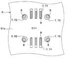
- a board 6 having signal lands 71 and auxiliary lands 72 is prepared, and solder 8 is applied onto the lands 71, 72 by printing.
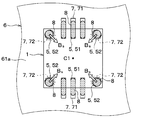
- the substrate 6 is provided with four circular auxiliary lands 72 in a plan view and is symmetrically arranged.
- the four auxiliary lands 72 are arranged in point symmetry with respect to the center C1 between the plurality of auxiliary lands 72, as shown in FIG. 4A.
- the center C1 is the center position between the four auxiliary lands 72 in a plan view, and in the present embodiment, the center position between the four auxiliary electrodes 52 when the semiconductor package 1 is mounted on the substrate 6. It is a part that overlaps with.
- the signal land 71 is applied to one end side where the semiconductor package 1 is mounted. Further, with respect to the auxiliary land 72, in the next step shown in FIG. 4B, the solder 8 is applied to at least a portion located in the inner region of the outer contour of the auxiliary electrode 51, and the remaining portion is exposed from the solder 8. This is to control the mounting posture of the semiconductor package 1 by causing the solder 8 applied to the auxiliary land 72 to flow toward the center C1 when melted in the reflow process.
- solder 8 When applying the solder 8 to the signal land 71 and the auxiliary land 72, it is desirable to apply the solder 8 to the inside of the outer contour of the lands 71 and 72. This is to prevent the solder 8 from protruding from the outer contours of the lands 71 and 72 when the semiconductor package 1 shown in FIG. 4B is mounted and from generating solder balls due to the protruding solder 8 during the reflow process.
- a semiconductor package 1 manufactured by a normal semiconductor process and provided with a signal electrode 51 and an auxiliary electrode 52 is prepared, and the semiconductor package 1 is placed on the substrate 6 while being aligned. ..
- the auxiliary electrode 52 has its center offset from the center of the auxiliary land 72, while the auxiliary electrode 52 is concentrically arranged with the solder 8.
- the semiconductor package 1 is placed on the substrate 6 so that More specifically, at this time, as shown in FIG. 4B, the four auxiliary lands 72 are offset such that the centers of the four auxiliary lands 72 are closer to the center C1 side than the centers of the opposing auxiliary electrodes 52.
- the solder 8 is melted by heating and the semiconductor package 1 and the substrate 6 are joined.
- the molten solder 8 on each auxiliary land 72 flows toward the center C1, and the semiconductor package 1 due to the surface tension of the molten solder 8 is moved to the center C1 as indicated by the white arrow.
- a force B s is drawn to the side.
- the pulling force B s is referred to as “surface tension vector B s ” for convenience of description.
- the surface tension vector B s is generated by the number of the four auxiliary lands 72 that are the attitude control lands in the present embodiment, and as shown by the white arrow in FIG. 4C, all of them are in the state of heading to the center C1.
- the surface tension vector B s is offset as a whole force by pulling each of the four corners of the semiconductor package 1 in the direction of the center C1, and acts to keep the semiconductor package 1 in a predetermined posture.
- the solder 8 applied on the signal land 71 is melted and spread like the solder 8 on the auxiliary land 72, and the outer contour of the signal electrode 51 overlaps the outer contour of the signal land 71.
- the solder 8 on the auxiliary land 72 causes a self-alignment action of preventing the semiconductor package 1 from tilting in an unintended direction, and the solder 8 on the signal land 71 self-aligns with the signal electrode 51.
- offset direction the direction from the center of the auxiliary electrode 52 to the center of the auxiliary land 72 in a straight line in plan view.
- the auxiliary electrode 52 is arranged inside the outer contour of the auxiliary land 72, and at least on the opposite side of the outer contour of the auxiliary electrode 52 to the outer contour of the auxiliary land 72. It is preferable that This is because in the solder joining process, almost all of the melted solder 8 spreads in the offset direction side so as to increase the accuracy of controlling the mounting attitude of the semiconductor package 1.
- the plurality of auxiliary lands 72 have a difference in heat capacity of not more than a predetermined value. This is to prevent the melting timing of the solder 8 on the plurality of auxiliary lands 72 from deviating, that is, reducing the effect of maintaining the mounting posture of the semiconductor package 1 due to the deviation of the generation timing of the surface tension vector B s. Is.
- An example of setting the difference in heat capacities to a predetermined value or less is, for example, making the areas of the auxiliary lands 72 the same or substantially the same, but is not limited to this.
- the solder 8 is re-cured, and the semiconductor package 1 is mounted and fixed on the substrate 6.
- the semiconductor device S1 mounted on the substrate 6 can be manufactured while the semiconductor package 1 maintains a predetermined mounting posture with respect to the one surface 61a which is the mounting surface of the substrate 6.
- auxiliary electrode 52 and the auxiliary land 72 that is, the pair of attitude control units in the present embodiment are arranged in point symmetry. Any symmetric arrangement that balances B s may be used.
- the auxiliary electrode 52 and the auxiliary land 72 may be arranged in line symmetry.
- the left-right direction on the paper surface is the X direction
- the direction orthogonal to the X direction on the paper surface is the Y direction
- the direction orthogonal to the XY plane is the Z direction.
- a part or all of the land 7 that is hidden by the semiconductor packages 1 and 110 and is not visible in a plan view is shown by a broken line
- the electrodes 5, 111 and 112 are shown by solid lines. It shows with.
- a semiconductor package 110 having a signal electrode 111 and an auxiliary electrode 112 is mounted on a substrate 120 having a signal land 121 and an auxiliary land 122 via solder 8.
- the signal land 121 has a plane size larger than that of the signal electrode 111
- the auxiliary land 122 has a plane size larger than that of the auxiliary electrode 112.
- the signal land 121 and the auxiliary land 122 have a shape in which the electrode 111 or 112 connected via the solder 8 is expanded in the same direction. Even with such a structure, since the amount of the solder 8 is increased, it is possible to secure the joining reliability after the solder joining.
- solder 8 applied on the lands 121 and 122 of the substrate 120 covers a part of the inside of the outer rim of the lands 121 and 122 and exposes the rest. This is to prevent the formation of solder balls or solder bridges due to the molten solder 8 protruding from the lands 121 and 122 when the semiconductor package 1 is mounted.
- the molten solder 8 spreads in the same direction on the lands 121 and 122 during solder joining, so that the semiconductor package 110 is in a state in which it is easy to swim until the solder 8 is rehardened. Will end up. If some external force is applied at this time, the semiconductor package 110 is mounted on the substrate 120 in a posture displaced in an unintended direction on the XY plane or the Z direction, as shown in FIG. 5B, for example.
- the semiconductor device S1 of this embodiment is manufactured in a state in which the mounting posture of the semiconductor package 1 is controlled by the surface tension vector as described above. Therefore, as shown in FIG. 6, the semiconductor device S1 has a structure in which the positional displacement between the semiconductor package 1 and the substrate 6 in the X direction, the Y direction, and the Z direction is suppressed.
- the semiconductor device S1 has an improved structure.
- the auxiliary electrode 52 and the auxiliary land 72 cause the surface tension vector B s that pulls the semiconductor package 1 in the predetermined direction by spreading the molten solder 8 in the predetermined direction in the solder joining process. It is arranged so as to be offset. Then, the plurality of auxiliary electrodes 52 and the auxiliary lands 72 are symmetrically arranged so that the surface tension vector B s generated in the solder joining process is in a balanced state, and the area of the auxiliary lands 72 is larger than that of the auxiliary electrodes 52. Therefore, the amount of the solder 8 is set to a predetermined amount or more.
- the mounting posture of the semiconductor package 1 is controlled and the amount of the solder 8 is set to a predetermined amount or more, so that the reliability of the solder joint can be secured, that is, the mounting posture
- the structure ensures both securing and reliability of solder bonding.
- the semiconductor device S1 whose mounting posture is controlled is mounted on a vehicle, for example, it is easier to match the detection axis of the physical quantity of the sensor unit 21 with the traveling direction of the vehicle.
- the structure is highly accurate and is particularly suitable for applications requiring sensor accuracy.
- the mounting posture of the semiconductor package 1 is controlled, the solder 8 melted in the solder joining process is suppressed from protruding outside the outer contour of the land 7, and thus the generation of solder balls and solder bridges is suppressed. The effect is also obtained.
- FIG. 7 as in FIG. 1, the outline of the semiconductor chip 2 which is not visible in a top view is indicated by a chain double-dashed line, and the outline of the signal land 71 hidden by the semiconductor package 1 and the outline of the auxiliary land 72 are indicated by broken lines. , The auxiliary electrode 52 is shown by a solid line. Further, in FIG. 7, for the same purpose as above, the solder 8 that is hidden by the semiconductor package 1 and is not visible in the top view is omitted. Although the cross section is not shown in FIG. 8, in order to make it easier to see and facilitate understanding, the solder 8 is hatched, and the outside of the semiconductor package 1, the electrodes 51 and 52, the substrate 6, the lands 71 and 72 and the solder 8 are excluded. The constituent elements of are omitted.
- the center of the auxiliary land 72 is arranged farther from the center C1 of the plurality of auxiliary electrodes 52 than the center of the auxiliary electrodes 52 facing each other in plan view. This is different from the first embodiment in that In the present embodiment, this difference will be mainly described.
- the semiconductor device S2 of the present embodiment is manufactured by the same manufacturing method as that of the first embodiment, but as shown in FIG. 8, for example, all of the plurality of surface tension vectors B s generated in the solder bonding step are semiconductors. It is configured to face the outside of the package 1.
- the auxiliary land 72 is arranged so as to include the auxiliary electrode 52 in a plan view, and has a shape extending in the radial direction with the center C1 as an axis. Further, in the step of applying the solder 8, the solder 8 is applied to at least a portion of the auxiliary land 72 located in the inner region of the outer contour of the auxiliary electrode 52, and then the semiconductor package 1 is mounted. Then, in the solder joining step, the molten solder 8 wets and spreads in a radial direction with the center C1 as an axis in a plan view, and a plurality of surface tension vectors B s pulling the semiconductor package 1 in the radial direction at the four corners thereof. Occurs.
- these surface tension vectors Bs are in the opposite direction to those of the first embodiment, they are in a state of being balanced as a whole force, and serve to prevent the semiconductor package 1 from tilting in an unintended direction. As a result, the semiconductor package 1 is mounted on the substrate 6 in a state where the mounting posture is controlled.
- the pair of attitude control units are symmetrically arranged as in the first embodiment, and the semiconductor device S2 can obtain the same effect as this.
- a semiconductor device S3 of the third embodiment will be described with reference to FIGS. 9 to 11B.
- FIGS. 9 and 10 the outline of the portion of the signal land 71 hidden in the semiconductor package 1 is shown by a broken line and the signal electrode 51 is shown by a solid line for easy viewing.
- the outer contour of the semiconductor chip 2 is further indicated by a chain double-dashed line.
- 11A and 11B the cross-section is not shown for the sake of clarity, but the solder 8 is hatched and the signal electrode 51 is shown by a thick solid line, and a portion of the signal land 71 that is hidden by the semiconductor package 1 and cannot be seen. Is indicated by a broken line.
- FIGS. 11A and 11B the direction in which the melted solder 8 spreads inside the outer contour of the semiconductor package 1 is indicated by an arrow.
- the semiconductor device S3 of the present embodiment does not have the auxiliary electrode 52 and the auxiliary land 72, and the signal electrode 51 and the signal land 71 are the attitude control electrode and the attitude control land, respectively. This is different from the first embodiment described above. In the present embodiment, this difference will be mainly described.
- the signal electrodes 51 extend so as to intersect the outer contour of the semiconductor package 1, and three signal electrodes 51 are arranged on each of the four sides of the outer contour. .. That is, in this embodiment, the semiconductor package 1 has a QFN structure.
- the plurality of signal electrodes 51 are connected to the signal lands 71 via the solder 8, and are arranged symmetrically with the signal lands 71 connected via the solder 8 in a plan view.
- the three signal electrodes 51 intersecting one side of the contour of the semiconductor package 1 are arranged symmetrically with respect to the central signal electrode 51. ing.
- the above-mentioned arrangement relationship of the plurality of signal electrodes 51 is the same for the other signal electrodes 51 intersecting with the other side forming the outline of the semiconductor package 1. That is, in the semiconductor device S3 of the present embodiment, the signal electrode 51 and the signal land 71 connected to the signal electrode 51 via the solder 8 are a pair of attitude control units, and the plurality of pair of attitude control units are the center of the semiconductor package 1. It is arranged symmetrically with respect to.
- the three signal electrodes 51 shown in FIG. 11A will be mainly described as a representative example.
- the signal electrode 51 at the left end of the paper among the three signal electrodes 51 shown in FIG. 11A is referred to as “left signal electrode 51”, and the central signal electrode 51 is referred to as “middle signal electrode 51”.
- the signal electrode 51 at the right end of the paper is referred to as "right signal electrode 51".
- each of the right signal electrode 51 and the left signal electrode 51 has a middle width in a direction parallel to one side of an outer contour of the semiconductor package 1 (hereinafter, referred to as “outer parallel direction”).
- the shape is smaller than the signal electrode 51 and the signal land 71.
- the right signal electrode 51 and the left signal electrode 51 have the same area and are arranged so as to overlap one side of the opposing signal lands 71 on the side of the middle signal electrode 51 as shown in FIG. 11A.
- the middle signal electrode 51 has the same width as the opposing signal land 71 in the outer contour parallel direction, and the outer contour thereof is arranged to overlap the outer contour of the signal land 71.
- the signal lands 71 are provided in the same number as the signal electrodes 51, and are arranged in a portion corresponding to the signal electrodes 51.
- the plurality of signal lands 71 have at least the same area as the area disposed inside the outer contour of the semiconductor package 1, and as shown in FIG. It is said that.
- the melted solder 8 spreads in the same direction immediately under the middle signal electrode 51 and spreads in the same direction right below the right signal electrode 51 mainly on the right side of the drawing as shown in FIG. 11B.
- the left signal electrode 51 it spreads mainly in the leftward direction on the paper surface. This is the same state on all four sides forming the outer contour of the semiconductor package 1.
- the semiconductor device S3 can obtain the same effect as that of the first embodiment.
- the cross section is not shown in FIG. 13 for clarity, the solder 8 is hatched, and the direction of the surface tension vector B s generated at the time of joining by the solder 8 is shown by a white arrow.
- the semiconductor device S4 of the present embodiment has only one auxiliary electrode 52 and one auxiliary land 72, and these are an attitude control electrode and an attitude control land. This is different from the first embodiment. In the present embodiment, this difference will be mainly described.
- auxiliary land 72 As shown in FIG. 12, there is only one auxiliary land 72 in this embodiment, and it functions as an attitude control land.
- the auxiliary land 72 has a plurality of extending portions 721 extending in the radial direction with the center of the semiconductor package 1 as an axis in a plan view in a state where the semiconductor package 1 is mounted. Become.
- the extension portion 721 is referred to as a “first extension portion 721” for convenience.
- the first extension portion 721 preferably has the same plane size and the same plane shape as the other first extension portions 721 in order to easily adjust the surface tension vector B s described later.
- the auxiliary electrode 52 is only one in this embodiment, functions as an attitude control electrode, and forms a pair of attitude control units together with the auxiliary land 72.
- the auxiliary electrode 52 is arranged so as to be included inside the outer contour of the auxiliary land 72 in plan view, and extends along the first extending portion 721.
- the plurality of extended second extending portions 521 are provided. That is, when the auxiliary land 72 has the four first extending portions 721, the auxiliary electrode 52 has the four second extending portions 521.
- the second extending portion 521 preferably has the same plane size and the same plane shape as the other second extending portions 521. Moreover, the number of the second extending portions 521 may be the same as the number of the first extending portions 721, and the number is appropriately changed.
- the first extending portion 721 protrudes outside the second extending portion 521 in the extending direction in plan view.
- the auxiliary land 72 has a plurality of outer portions 722, with a portion of the first extended portion 721 outside the outer contour of the opposing second extended portion 521 being the outer portion 722.
- the plurality of outer portions 722 are arranged symmetrically with respect to the center of the semiconductor package 1, for example, line symmetrical or point symmetrical in order to adjust the surface tension vector B s to ensure the mounting posture of the semiconductor package 1. ing.
- the plurality of outer portions 722 are regions where the molten solder 8 spreads when the semiconductor package 1 is joined by the solder 8 as shown in FIG.
- the symmetrical arrangement of the plurality of outer portions 722 causes the surface tension vectors B s generated in the plurality of outer portions 722 to cancel each other, as shown in FIG. 13.
- the semiconductor device S4 has a structure in which the amount of the solder 8 is increased and the semiconductor package 1 is suppressed from unintentional movement during solder joining.
- the pair of attitude control units are arranged near the center of the mounting surface of the semiconductor package 1 and can be used to secure the heat dissipation of the semiconductor package 1 after solder bonding.
- the outer portion 722 has the same or substantially the same plane as the other outer portions 722 when the plurality of first extending portions 721 and the second extending portions 521 have the same or similar plane size and shape. It is preferably sized.
- the attitude control land and the attitude control electrode are arranged such that their centers are offset in a plan view, but in the present embodiment, these centers overlap. It may be arranged.
- the semiconductor package 1 may have a structure that functions as a physical quantity sensor, and the semiconductor chip 2 may be covered with mold resin except the sensor portion 21, or any other structure may be adopted. May be.
- attitude control electrode of the electrode 5 and the attitude control land of the land 7 are symmetrically arranged.
- this symmetrical arrangement does not mean only when the contours of the attitude control electrodes and the attitude control lands are the same when they are rotated with respect to a predetermined point or bent with respect to a predetermined line. ..
- the symmetrical arrangement here also includes, for example, the case where the outer contours of at least the portions where the solder 8 spreads out of the attitude control lands are the same.
- the plurality of attitude control lands are located closer to the outer center of the semiconductor package 1 than the center of the attitude control electrodes whose centers are opposed to each other in plan view, or The example in which it is arranged at a distant position has been described.
- the attitude control electrodes and the attitude control lands have only to be arranged so that a plurality of surface tension vectors B s generated at the time of joining with the solder 8 cancel each other out and balance each other, and the above arrangement and number are limited. It is not something that will be done.
- one posture control electrode and one posture control land are arranged at the four corners of the outer shape of the quadrangular plate-shaped semiconductor package 1, that is, a total of four electrodes and lands are arranged, May be done.
- the center of the attitude control land is closer to the center of the semiconductor package 1 than the center of the attitude control electrode, and the remaining The two may be arranged in the opposite relationship.
- the plurality of surface tension vectors B s cancel and balance each other, so that the semiconductor package 1 is prevented from tilting in an unintended direction.
- the arrangement of the attitude control electrodes and the attitude control lands may be changed as described above, or may be another arrangement in which the surface tension vector B s is balanced, and the numbers thereof are also appropriately changed. May be.
- attitude control electrodes and the attitude control lands may be the same number and symmetrically arranged in the above meaning, and are not limited to the numbers described in the above embodiments.
- the land 7 for mounting the semiconductor package 1 may be used and may not necessarily be the substrate.
Landscapes
- Engineering & Computer Science (AREA)
- Microelectronics & Electronic Packaging (AREA)
- Physics & Mathematics (AREA)
- Condensed Matter Physics & Semiconductors (AREA)
- General Physics & Mathematics (AREA)
- Computer Hardware Design (AREA)
- Power Engineering (AREA)
- Manufacturing & Machinery (AREA)
- Geometry (AREA)
- Wire Bonding (AREA)
- Electric Connection Of Electric Components To Printed Circuits (AREA)
Abstract
半導体装置であって、複数の電極(5)を備える半導体パッケージ(1)と、複数のランド(7)を備え、半導体パッケージが搭載される被搭載物(6)と、を備え、半導体パッケージは、複数の電極が複数のランドとはんだ(8)を介して接続される。複数の電極のうち1つは、半導体パッケージの姿勢制御用電極であり、複数のランドのうち1つは、半導体パッケージの姿勢制御用ランドである。姿勢制御用ランドは、平面視にて、姿勢制御用電極を内包する配置とされ、半導体パッケージの中心を軸とする径方向であってそれぞれ異なる方向に延設された複数の延設部(721)を有する。姿勢制御用電極は、複数の延設部をそれぞれ第1延設部として、第1延設部に沿って延設された複数の第2延設部(521)を有し、平面視にて第1延設部のうち対向する第2延設部の外郭よりも外側の部分である外側部(722)は、半導体パッケージの中心に対して対称配置される。
Description
本出願は、2019年1月10日に出願された日本特許出願番号2019-2913号に基づくもので、ここにその記載内容が参照により組み入れられる。
本開示は、複数の電極を備える半導体パッケージがはんだを介して搭載された構造の半導体装置およびその製造方法に関する。
従来から、複数の電極を備える半導体パッケージとランドが形成されたプリント基板とがはんだを介して接合されてなる半導体装置においては、半導体パッケージが、その電極がプリント基板のランド位置とずれて載置されることがある。このような場合、半導体パッケージが予定された位置と異なる位置でプリント基板と接続されてしまい、半導体装置の不具合の原因となり得る。
さて、半導体パッケージの電極がプリント基板のランド位置とずれた位置に載置された場合であっても、これらを接合する際に溶融したはんだの表面張力により、半導体パッケージがランド位置に合わせて移動し、位置ズレが矯正される現象が知られている。この現象は、セルフアライメントと呼ばれる。このセルフアライメントを利用し、半導体パッケージの位置ズレを抑制できるプリント基板としては、例えば、特許文献1に記載のものが提案されている。このプリント基板は、半導体パッケージから突出する複数の電極のうちの1つと接続されるランドを複数備えてなり、当該複数の電極のうち端部に位置するものと対応するランドが、他のランドよりも大きな面積の大ランドとされている。また、このプリント基板は、大ランドと異なる他のランドが面積の小さい小ランドとされている。
これにより、配置間隔が狭い複数の電極を備える半導体パッケージを搭載でき、大ランド上のはんだ量を多くすることでセルフアライメントの効果を確保できる構成のプリント基板となる。
ところで、近年、電子機器の小型化に伴い、半導体パッケージの小型化が進んでおり、パッケージの外郭から突出する電極を有しないSON(Small Outline Non-leadの略)構造やQFN(Quad Flat Non-leadの略)構造が採用されることが増えている。この種の半導体パッケージは、プリント基板などにはんだ接合した後に、半導体パッケージとプリント基板との線膨張係数差などに起因する応力がはんだに生じた場合、電極による応力緩和の効果が小さく、その接合の信頼性が不十分となり得る。
はんだ接合の信頼性を確保するための方法としては、接合に用いるはんだの量を増やし、はんだによって応力を緩和することが考えられる。しかしながら、この方法では、例えば半導体パッケージを基板上にマウントする際に、はんだがランドからはみ出してその一部が分離すると、はんだボールが生じてしまい、他の電気的な不具合が生じ得る。また、この方法では、はんだが溶融して再硬化するまでの間における半導体パッケージの動きが大きくなり、半導体パッケージが基板に実装された後の姿勢(以下「実装姿勢」という)がずれてしまう。
なお、ここでいう「実装姿勢がずれる」とは、半導体パッケージが搭載される基板等の被搭載物のなす面に対して半導体パッケージが傾いた状態となること、および電極と被搭載物との位置がずれることのうち少なくとも一方の状態となることを意味する。
このような半導体パッケージの実装姿勢のずれは、例えば加速度や角速度などの所定の物理量が印加された際にこれに対応した信号を出力するセンサ部を備える半導体装置を構成する場合、センサの精度低下の原因となるため、問題となる。QFN構造などの半導体パッケージと特許文献1に記載のプリント基板とを用いて半導体装置を構成する場合、セルフアライメントにより電極とランドとの位置ズレについては抑制できるが、実装姿勢のずれについては対応できない。
本開示は、複数の電極を備える半導体パッケージがはんだを介して搭載されてなり、半導体パッケージの実装姿勢の確保とはんだ接合の信頼性確保とを両立できる半導体装置およびその製造方法を提供することを目的とする。
上記目的を達成するため、本開示の第1の観点による半導体装置は、複数の電極を備える半導体パッケージと、複数のランドを備え、半導体パッケージが搭載される被搭載物と、を備える。このような構成において、半導体パッケージは、複数の電極が複数のランドとはんだを介して接続されており、複数の電極のうち少なくとも一部の電極は、被搭載物のうち半導体パッケージと向き合う搭載面に対する半導体パッケージの姿勢を制御するために用いられる姿勢制御用電極であり、複数のランドのうち少なくとも一部のランドは、搭載面に対する半導体パッケージの姿勢を制御するために用いられる姿勢制御用ランドであり、姿勢制御用電極は、姿勢制御用ランドと重畳すると共に、平面視にて姿勢制御用電極の中心がはんだを介して接続された姿勢制御用ランドの中心とずらして配置されており、姿勢制御用ランドおよび姿勢制御用電極は、複数設けられており、姿勢制御用ランドおよび当該姿勢制御用ランドにはんだを介して接続された姿勢制御用電極を一対の姿勢制御部として、一対の姿勢制御部は、平面視にて半導体パッケージの中心に対して対称配置されている。
これにより、半導体パッケージが基板上に搭載され、姿勢制御用電極およびこれにはんだを介して接続された姿勢制御用ランドによりなる一対の姿勢制御部を複数備え、一対の姿勢制御部が平面視にて半導体パッケージの中心に対して対称配置された構造となる。一対の姿勢制御部は、はんだを介して接続される際に溶融したはんだが濡れ広がることで、溶融したはんだの表面張力に起因する力、すなわち表面張力ベクトルが生じる部分である。複数の一対の姿勢制御部が平面視にて半導体パッケージの中心に対して対称配置されることで、はんだ接合時に生じる複数の表面張力ベクトルが互いに打ち消し合う作用が生じる。そのため、はんだ接合に用いるはんだの量を増やしつつも、はんだ接合時において半導体パッケージの意図しない動きが抑制された状態で基板上に搭載されることとなり、半導体パッケージの実装姿勢の確保とはんだ接合の信頼性確保とを両立できる。
本開示の第2の観点による半導体装置は、複数の電極を備える半導体パッケージと、複数のランドを備え、半導体パッケージが搭載される被搭載物と、を備え、半導体パッケージは、複数の電極が複数のランドとはんだを介して接続されており、複数の電極のうち1つの電極は、被搭載物のうち半導体パッケージと向き合う搭載面に対する半導体パッケージの姿勢を制御するために用いられる姿勢制御用電極であり、複数のランドのうち1つのランドは、搭載面に対する半導体パッケージの姿勢を制御するために用いられる姿勢制御用ランドであり、姿勢制御用ランドは、姿勢制御用電極よりも平面サイズが大きく、かつ、平面視にて、姿勢制御用電極を内包する配置とされると共に、半導体パッケージの中心を軸とする径方向に延設された複数の延設部を有しており、複数の延設部は、それぞれ径方向のうち異なる方向に沿って延設されており、姿勢制御用電極は、複数の延設部をそれぞれ第1延設部として、第1延設部に沿って延設された複数の第2延設部を有しており、平面視にて第1延設部のうち対向する第2延設部の外郭よりも外側の部分を外側部として、外側部は、半導体パッケージの中心に対して対称配置されている。
これにより、姿勢制御用電極および姿勢制御用ランドをそれぞれ1つのみ有する半導体装置であっても、上記第1の観点による半導体装置と同様に、はんだの量を確保しつつも、はんだ接合時における表面張力ベクトルが相殺される構造となる。そのため、第2の観点による半導体装置においても、上記第1の観点による半導体装置と同様の効果が得られる。
本開示の第3の観点による半導体装置の製造方法は、複数の電極を備える半導体パッケージと複数のランドを備える被搭載物とがはんだを介して接続された半導体装置の製造方法であって、半導体パッケージを用意することと、被搭載物を用意することと、被搭載物のランド上にはんだを塗布することと、半導体パッケージをはんだが塗布された被搭載物上に搭載することと、を含む。このような構成において、半導体パッケージを用意することにおいては、複数の電極のうち少なくとも2以上の電極を、被搭載物のうち半導体パッケージと向き合う搭載面に対する半導体パッケージの姿勢を制御するための姿勢制御用電極とし、被搭載物を用意することにおいては、複数のランドのうち少なくとも2以上のランドを、搭載面に対する半導体パッケージの姿勢を制御するための姿勢制御用ランドとし、はんだを塗布することにおいては、姿勢制御用ランドのうち一部の領域をはんだから露出させ、半導体パッケージを被搭載物上に搭載することにおいては、姿勢制御用電極と姿勢制御用ランドとを互いの中心をずらして配置した状態ではんだにより接合し、はんだによる接合においては、平面視にて、溶融させたはんだを姿勢制御用ランドのうち姿勢制御用ランドの外郭よりも内側の領域から外側の領域に濡れ広がらせると共に、この濡れ広がりにおける溶融したはんだの表面張力による半導体パッケージの引張方向を表面張力ベクトルとして、各姿勢制御用電極上に塗布したはんだによる表面張力ベクトル全体が釣り合う状態とする。
これにより、半導体パッケージを基板上に搭載する工程にて、半導体パッケージの複数の姿勢制御用電極と基板の複数の姿勢制御用ランドとをはんだを介して接合する際に複数の表面張力ベクトルが生じる。このとき、平面視にて、姿勢制御用電極と姿勢制御用ランドとが互いの中心をずらして配置されると共に、姿勢制御用ランドの一部がはんだから露出しているため、はんだ接合の際に溶融したはんだが当該露出した部分に濡れ広がることになる。また、濡れ広がりにおける溶融したはんだの表面張力による半導体パッケージの引張方向を表面張力ベクトルとして、各姿勢制御用電極上に塗布したはんだによる表面張力ベクトル全体が釣り合う状態とする。したがって、はんだを溶融させてから再硬化させるまでの間、半導体パッケージが意図しない動きをすることが抑制され、半導体パッケージの姿勢制御がされた状態で基板上に搭載された構成の半導体装置を製造することができる。
なお、各構成要素等に付された括弧付きの参照符号は、その構成要素等と後述する実施形態に記載の具体的な構成要素等との対応関係の一例を示すものである。
以下、本開示に係る半導体装置の実施形態について図に基づいて説明する。なお、以下の各実施形態相互において、互いに同一もしくは均等である部分には、同一符号を付して説明を行う。
(第1実施形態)
第1実施形態の半導体装置S1について、図1~図3を参照して述べる。本実施形態の半導体装置S1は、例えば、自動車などの車両に搭載され、加速度や角速度などの物理量が印加された際に当該物理量に応じた信号を出力する物理量センサを備える電子部品に適用されると好適である。例えば、半導体装置S1は、加速度が印加されるとその加速度に応じた信号を出力する加速度センサを備える構成とされ、エアバッグなどの車両の乗員保護装置等のセンサ精度が求められる用途に適用され得るが、他の用途にも適用され得る。
第1実施形態の半導体装置S1について、図1~図3を参照して述べる。本実施形態の半導体装置S1は、例えば、自動車などの車両に搭載され、加速度や角速度などの物理量が印加された際に当該物理量に応じた信号を出力する物理量センサを備える電子部品に適用されると好適である。例えば、半導体装置S1は、加速度が印加されるとその加速度に応じた信号を出力する加速度センサを備える構成とされ、エアバッグなどの車両の乗員保護装置等のセンサ精度が求められる用途に適用され得るが、他の用途にも適用され得る。
図1では、見易くして構成の理解を助けるため、上面視では見えない後述の半導体チップ2の外郭を二点鎖線で、信号ランド71のうち半導体パッケージ1に隠された部分の外郭および補助ランド72の外郭を破線で、補助電極52を実線で示している。また、図1では、上記と同様の目的で、上面視にて、後述するはんだ8のうち半導体パッケージ1に隠されて見えないものを省略している。
(構成)
本実施形態の半導体装置S1は、図1に示すように、電極5を備える半導体パッケージ1と、導電性のランド7を備える基板6とを備え、これらがはんだ8を介して電気的に接続されてなる。半導体装置S1は、半導体パッケージ1が、基板6のうち半導体パッケージ1と向き合う搭載面、すなわち一面61aに対して略平行、かつ上面視にて後述する信号電極51と信号ランド71とが位置合わせされた状態で実装された構成とされている。
本実施形態の半導体装置S1は、図1に示すように、電極5を備える半導体パッケージ1と、導電性のランド7を備える基板6とを備え、これらがはんだ8を介して電気的に接続されてなる。半導体装置S1は、半導体パッケージ1が、基板6のうち半導体パッケージ1と向き合う搭載面、すなわち一面61aに対して略平行、かつ上面視にて後述する信号電極51と信号ランド71とが位置合わせされた状態で実装された構成とされている。
以下、説明の簡略化のため、上記した半導体パッケージ1の実装状態を「実装姿勢が制御された状態」と称する。
半導体パッケージ1は、例えば、図2もしくは図3に示すように、センサ部21を有する半導体チップ2と、これを収容する凹部および電極5を備える筐体4と、これらを電気的に接続するワイヤ3とを備える。半導体パッケージ1は、例えば、上面視にて、電極51、52が半導体パッケージ1の外郭の内側に配置された構造とされており、本実施形態では、SON構造とされている。半導体パッケージ1は、例えば図2に示すように、半導体チップ2のセンサ部21がワイヤ3、電極42および配線43を介して、筐体4の外部に露出している信号電極51と電気的に接続され、外部にセンサ部21の信号を出力する。
半導体チップ2は、例えば、主としてシリコンなどの半導体材料によりなり、通常の半導体プロセスにより製造される。半導体チップ2は、図2に示すように、半導体チップ2に物理量が印加されると、当該物理量に応じた信号を出力するセンサ部21が形成されている。半導体チップ2は、例えば、図2に示すように、不図示のダイボンド材を介して筐体4の凹部の底面上に搭載され、ワイヤ3を介して凹部内の電極42に電気的に接続されている。
なお、図2、図3では、センサ部21を備える半導体チップ2が筐体4の凹部に不図示のダイボンド材を介して搭載され、凹部の内部に形成された電極42にワイヤ3を介して直接的に接続された例を示しているが、これに限定されるものではない。例えば、半導体チップ2を回路素子が形成された他のシリコン基板によりなる回路チップ上に搭載され、回路チップにワイヤ3で接続されると共に、回路チップと電極42とが別のワイヤで接続され、半導体チップ2が信号電極51と接続される構造でもよい。この場合、回路チップが筐体4の凹部の底面上に不図示のダイボンド材を介して搭載される。このように、半導体チップ2の筐体4への搭載や信号電極51への接続については、適宜変更されてもよい。
センサ部21は、例えば、加速度や角速度などの物理量が印加された際に、当該物理量に応じた信号を出力する任意の構成とされている。センサ部21は、例えば、錘として機能する可動部に櫛歯型電極が形成され、静電容量の変化を検出する構成とされてもよいし、ピエゾ抵抗素子を用いて物理量が印加された際の歪みを検出する方式であってもよく、任意の構成とされる。
なお、半導体パッケージ1は、センサ部21が加速度に応じた信号を出力する構成の場合には、加速度センサとして機能し、センサ部21が角速度に応じた信号を出力する構成の場合には、角速度センサとして機能する。また、センサ部21は、加速度センサや角速度センサなどの公知のセンサ構造が採用され得るため、本明細書では、センサ構造についての詳細な説明を省略する。
ワイヤ3は、例えば、金などの金属材料によりなる接続部材であり、ワイヤボンディングなどにより半導体チップ2および筐体4の電極42それぞれに接続される。
筐体4は、例えば図2に示すように、半導体チップ2が収容される凹部を備える本体部41と、凹部に形成された電極42と、外部に露出した信号電極51および補助電極52と、電極42と信号電極51とを電気的に接続する配線43と、蓋部44とを備える。
本体部41は、例えばアルミナなどのセラミックスで構成されている。本体部41は、例えば金属材料などで構成された蓋部44がはんだ付けなどにより凹部を覆うように接続された構成とされ、半導体チップ2を覆って保護している。
電極5は、本実施形態では、図2もしくは図3に示すように、半導体チップ2から出力された信号が伝送される複数の信号電極51と、信号の伝送などには用いられない複数の補助電極52とによりなる。信号電極51および補助電極52は、はんだ8を介して基板6に形成された導電性のランド7に接続されている。
信号電極51は、その外郭が例えば図1に示す基板6の信号ランド71の外郭の一部と位置合わせされた状態で配置され、図2に示すように、はんだ8を介して信号ランド71と電気的に接続されている。信号電極51は、例えば、四角形板状とされるが、その形状は任意である。信号電極51は、複数設けられ、例えば図1に示すように、上面視した際に筐体4の本体部41の外周部分に互いに距離を隔てて配置される。
補助電極52は、例えば図1に示すように、複数設けられ、平面視にて円形状とされると共に、半導体パッケージ1の外郭の四隅それぞれに1つずつ配置されている。補助電極52は、図3に示すように、はんだ8を介して基板6の補助ランド72に接続されている。なお、補助電極52は、平面視にて円形状だけでなく、楕円形状や多角形状であってもよいし、他の任意の形状であってもよい。
本実施形態では、補助電極52は、基板6の補助ランド72と共に、半導体パッケージ1が基板6上での実装姿勢を制御するために用いられるダミーの電極であり、「姿勢制御用電極」と称され得る。複数の補助電極52は、半導体パッケージ1の実装姿勢を制御するため、後述の重畳する複数の補助ランド72と共に、平面視にて半導体パッケージ1の中心に対して対称配置とされている。この理由については、半導体装置S1の製造方法の説明にて後述する。
基板6は、例えば図2に示すように、基材61と、半導体パッケージ1を搭載するためのランド7とを備え、ランド7のうち信号ランド71に接続される不図示の回路配線が形成された配線基板である。基板6は、半導体パッケージ1を実装できる構成とされていればよく、ランド7のほか図示しない他の電子部品などが搭載するためのランドなどを備えていてもよいし、その構成については適宜変更される。
なお、基板6は、半導体パッケージ1が搭載される「被搭載物」に相当する。本実施形態では、被搭載物が、基板6である例について説明する。
基材61は、例えば図2もしくは図3に示すように、一面61aを有する板状とされ、例えばガラスエポキシ樹脂などの任意の材料により構成される。基材61の一面61a上には、ランド7が形成されている。
ランド7は、例えば銅などの金属材料により構成され、信号電極51がはんだ8を介して接続される信号ランド71と、補助電極52がはんだ8を介して接続される補助ランド72とによりなる。
信号ランド71は、基材61の一面61a上に複数設けられ、半導体パッケージ1の信号電極51と電気的に接続されると共に、不図示の配線が接続されており、半導体チップ2から出力された信号が伝送される。信号ランド71は、例えば四角形板状とされ、半導体パッケージ1の信号電極51の位置に合わせた配置とされている。本実施形態では、複数の信号ランド71は、例えば図1に示すように、上面視にてその延設方向を揃えた状態で互いに距離を隔てて配置されるが、これに限定されず、その配置や数については信号電極51に合わせて適宜変更される。
補助ランド72は、半導体パッケージ1の補助電極52と対をなす部材であり、例えば図3に示すように、基材61の一面61a上に複数設けられると共に、半導体パッケージ1の実装姿勢の制御に用いられる。複数の補助ランド72は、例えば平面視にて円形状とされ、半導体パッケージ1の補助電極52の位置に合わせた配置、すなわち補助電極52と同様に対称配置とされている。なお、補助ランド72は、平面視での形状が円形状だけでなく、楕円形状や多角形状であってもよいし、他の任意の形状でもよい。
補助ランド72は、はんだ8の量を多く確保し、半導体パッケージ1との接合信頼性を向上させるため、補助電極52よりもその平面サイズが大きくされている。複数の補助ランド72は、半導体パッケージ1を実装する際に溶融させるはんだ8の流れを制御するため、例えば、その中心が補助電極51の中心から所定の方向にオフセットされた配置とされている。この配置の詳細およびその効果については、後述する。
なお、補助ランド72は、本実施形態では、半導体パッケージ1の補助電極52と共に、半導体パッケージ1の実装姿勢を制御するために用いられるダミーのランドであり、「姿勢制御用ランド」と称され得る。
はんだ8は、ランド71、72上に例えば印刷により形成され、半導体パッケージ1の実装に用いられる。
なお、姿勢制御用ランドおよび当該姿勢制御用ランドにはんだ8を介して接続された姿勢制御用電極は、以下の説明において、便宜的に「一対の姿勢制御部」と称されることがある。つまり、半導体装置S1は、「一対の姿勢制御部」を複数備えると共に、これらの一対の姿勢制御部が、平面視にて半導体パッケージ1の中心に対して対称配置された構成とされている。
以上が、本実施形態の半導体装置S1の基本的な構成である。
(製造方法)
次に、本実施形態の半導体装置S1の製造方法の一例について、図4A~図4Cを参照して説明する。
次に、本実施形態の半導体装置S1の製造方法の一例について、図4A~図4Cを参照して説明する。
図4A~図4Cでは、断面を示すものではないが、見易くして理解を助けるため、はんだ8にハッチングを施している。図4B、図4Cでは、見易くするため、半導体パッケージ1の外郭、電極51、52、基板6、ランド71、72およびはんだ8以外の構成要素については省略している。
なお、半導体装置S1は、後述するはんだ8による接合工程での実装姿勢の制御を除き、任意の半導体装置の製造工程を採用できるため、本明細書では、実装姿勢の制御に関連する工程を主に説明する。
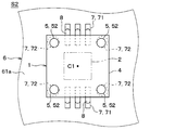
まず、図4Aに示すように、信号ランド71および補助ランド72を備える基板6を用意し、ランド71、72上に印刷によりはんだ8を塗布する。この基板6は、例えば、図4Aに示すように、平面視にて円形状の補助ランド72を4つ備え、対称配置とされている。具体的には、4つの補助ランド72は、図4Aに示すように、複数の補助ランド72の間の中心C1に対して点対称となる配置とされている。この中心C1は、平面視にて4つの補助ランド72の間の中心位置であり、本実施形態では、半導体パッケージ1を基板6上に載置した際の4つの補助電極52の間の中心位置と重なる部位である。
はんだ8の塗布においては、図4Aに示すように、信号ランド71については半導体パッケージ1が実装される一端側に塗布する。また、補助ランド72については、図4Bに示す次の工程において、少なくとも補助電極51の外郭の内側領域に位置する部分にはんだ8を塗布し、残部をはんだ8から露出した状態にする。これは、補助ランド72に塗布したはんだ8がリフロー工程において溶融した際に、いずれも中心C1に向けて流れるようにし、半導体パッケージ1の実装姿勢を制御するためである。
なお、信号ランド71および補助ランド72へのはんだ8の塗布においては、ランド71、72の外郭よりも内側に塗布することが望ましい。これは、図4Bに示す半導体パッケージ1のマウント時にはんだ8が、ランド71、72の外郭からはみ出し、リフロー工程時にこのはみ出したはんだ8によりはんだボールが生じることを抑制するためである。
続いて、図4Bに示すように、通常の半導体プロセスで製造され、信号電極51および補助電極52を備える半導体パッケージ1を用意し、半導体パッケージ1を基板6上に位置合わせしつつ、載置する。具体的には、図4Bに示すように、上面視にて、補助電極52がその中心が補助ランド72の中心とオフセットされた状態としつつ、補助電極52がはんだ8と同心配置された状態となるように半導体パッケージ1を基板6上に載置する。より具体的には、このとき、4つの補助ランド72は、図4Bに示すように、それぞれの中心が対向する補助電極52の中心よりも中心C1側に近い位置にオフセットされている。
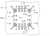
次いで、加熱によりはんだ8を溶融させ、半導体パッケージ1と基板6とを接合する。このとき、図4Cに示すように、各補助ランド72上の溶融したはんだ8が中心C1に向かって流れ、白抜き矢印で示すように、溶融したはんだ8の表面張力による半導体パッケージ1を中心C1側に引き込む力Bsが生じる。以下、この引き込む力Bsを、説明の便宜上、「表面張力ベクトルBs」と称する。
表面張力ベクトルBsは、本実施形態において姿勢制御用ランドである4つの補助ランド72の数だけ生じると共に、図4Cの白抜き矢印で示すように、いずれも中心C1に向かう状態となる。その結果、表面張力ベクトルBsは、本実施形態では、半導体パッケージ1の四隅それぞれを中心C1の方向に引っ張ることで力全体として相殺され、半導体パッケージ1を所定の姿勢に留めるように作用する。
なお、このとき、信号ランド71上に塗布されたはんだ8は、補助ランド72上のはんだ8と同様に溶融して濡れ広がり、信号電極51の外郭が信号ランド71の外郭と重なる、セルフアライメントの作用を生じさせる。つまり、補助ランド72上のはんだ8が、半導体パッケージ1が意図しない方向に傾くことを抑止するセルフアライメントの作用を生じさせ、信号ランド71上のはんだ8が信号電極51との位置合わせをするセルフアライメントの作用を生じさせる。
ここで、以下の説明において、平面視にて、補助電極52の中心から補助ランド72の中心へ直線状に向かう方向を、便宜上、「オフセット方向」と称する。
また、補助電極52は、図4Cに示すように、補助ランド72の外郭の内側に配置されると共に、補助電極52の外郭のうち少なくともオフセット方向の反対側にて補助ランド72の外郭と重なる配置とされることが好ましい。これは、はんだ接合工程において、溶融したはんだ8のほぼすべてがオフセット方向側に濡れ広がるようにし、半導体パッケージ1の実装姿勢の制御の精度を高めるためである。
さらに、補助ランド72上のはんだ8によるセルフアライメントの効果を確保する観点から、複数の補助ランド72は、熱容量の差が所定以下の状態とされることが好ましい。これは、複数の補助ランド72上のはんだ8の溶融タイミングがずれること、すなわち表面張力ベクトルBsの発生タイミングのずれによって、半導体パッケージ1の実装姿勢を維持する効果が低減することを抑止するためである。熱容量の差が所定以下の状態とする例としては、例えば、各補助ランド72の面積を同一もしくは同程度にすることなどが挙げられるが、これに限定されるものではない。
最後に、はんだ8を再硬化させて、半導体パッケージ1を基板6上に搭載して固定する。以上の工程により、半導体パッケージ1が、基板6の搭載面である一面61aに対して所定の実装姿勢を維持したまま、基板6上に実装された半導体装置S1を製造することができる。
なお、上記の説明では、補助電極52および補助ランド72、すなわち本実施形態における一対の姿勢制御部が点対称となる配置とされた例について説明したが、はんだ接合工程において生じる複数の表面張力ベクトルBsが釣り合う対称配置であればよい。例えば、補助電極52および補助ランド72は、線対称となる配置とされてもよい。
(半導体パッケージの実装姿勢制御)
ここで、補助電極52および補助ランド72の配置による半導体パッケージ1の実装姿勢の制御について、図5A、図5Bおよび図6を参照して説明する。
ここで、補助電極52および補助ランド72の配置による半導体パッケージ1の実装姿勢の制御について、図5A、図5Bおよび図6を参照して説明する。
図5Aないし図6では、説明の簡便化のため、紙面上の左右方向をX方向とし、紙面上においてX方向と直交する方向をY方向とし、XY平面に対して直交する方向をZ方向としている。また、図5Aないし図6では、見易くするため、平面視にて半導体パッケージ1、110に隠れて見えない部分のうちランド7の一部または全部を破線で示し、電極5、111、112を実線で示している。
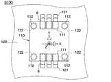
まず、比較のために、従来の半導体装置S100について、図5Aおよび図5Bを参照して説明する。
従来の半導体装置S100は、例えば図5Aに示すように、信号電極111および補助電極112を有する半導体パッケージ110が、信号ランド121および補助ランド122を有する基板120上にはんだ8を介して搭載されてなる。半導体装置S100は、信号ランド121が信号電極111よりも平面サイズが大きく、補助ランド122が補助電極112よりも平面サイズが大きくされている。換言すると、半導体装置S100は、信号ランド121および補助ランド122が、はんだ8を介して接続される電極111または112を等方向に広げた形状とされている。このような構造であっても、はんだ8の量が増加するため、はんだ接合後の接合信頼性を確保することができる。
なお、基板120のランド121、122上に塗布するはんだ8は、ランド121、122の外郭よりも内側の一部を覆い、残部を露出した状態とされる。これは、半導体パッケージ1のマウント時に、ランド121、122から溶融したはんだ8がはみ出すことによるはんだボールやはんだブリッジが形成されることを抑制するためである。
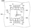
しかしながら、このような構造の場合、はんだ接合の際、溶融したはんだ8がランド121、122上において等方向に広がるため、はんだ8を再硬化させるまでの間、半導体パッケージ110が泳ぎやすい状態となってしまう。この際に何らかの外力が作用した場合、例えば図5Bに示すように、半導体パッケージ110は、XY平面上やZ方向において意図しない方向にずれた姿勢で基板120上に搭載されてしまう。
これに対して、本実施形態の半導体装置S1は、上述したように表面張力ベクトルにより半導体パッケージ1の実装姿勢を制御した状態で製造される。そのため、半導体装置S1は、図6に示すように、X方向、Y方向、Z方向における半導体パッケージ1と基板6との位置ズレが抑制された構造となる。
また、補助ランド72の面積が補助電極52よりも大きくされているため、補助ランド72上のはんだ8の量を増やすことができ、補助電極52と補助ランド72とのはんだ8による接合の信頼性を高められた構造の半導体装置S1となる。
本実施形態によれば、補助電極52と補助ランド72とが、はんだ接合工程において、溶融したはんだ8が所定の方向に濡れ広がり、所定の方向に半導体パッケージ1を引っ張る表面張力ベクトルBsを生じさせるようにオフセットされた配置とされている。そして、はんだ接合工程にて生じる表面張力ベクトルBsが釣り合う状態となるように、複数の補助電極52および補助ランド72とが対称配置とされ、かつ補助ランド72の面積が補助電極52よりも大きくされ、はんだ8の量が所定以上とされている。
そのため、本実施形態の半導体装置S1は、半導体パッケージ1の実装姿勢が制御された状態となると共に、はんだ8の量が所定以上とされ、はんだ接合の信頼性を確保できる構造、すなわち実装姿勢の確保とはんだ接合の信頼性確保とを両立できる構造となる。
また、実装姿勢が制御された半導体装置S1は、例えば車両に搭載された場合、センサ部21の物理量の検出軸と当該車両の進行方向とを一致させることが容易であるため、従来よりもセンサ精度が高く、センサ精度が求められる用途に特に適した構成となる。
さらに、半導体パッケージ1の実装姿勢が制御されることで、はんだ接合工程にて溶融したはんだ8がランド7の外郭よりも外側にはみ出すことが抑制されるため、はんだボールやはんだブリッジの発生が抑制される効果も得られる。
(第2実施形態)
第2実施形態の半導体装置S2について、図7、図8を参照して述べる。
第2実施形態の半導体装置S2について、図7、図8を参照して述べる。
図7では、図1と同様に、上面視では見えない半導体チップ2の外郭を二点鎖線で、信号ランド71のうち半導体パッケージ1に隠された部分の外郭および補助ランド72の外郭を破線で、補助電極52を実線で示している。また、図7では、上記と同様の目的で、上面視にて、はんだ8のうち半導体パッケージ1に隠されて見えないものを省略している。図8では、断面を示すものではないが、見易くして理解を助けるため、はんだ8にハッチングを施すと共に、半導体パッケージ1の外郭、電極51、52、基板6、ランド71、72およびはんだ8以外の構成要素については省略している。
本実施形態の半導体装置S2は、図7に示すように、平面視にて、補助ランド72の中心が、対向する補助電極52の中心よりも複数の補助電極52の中心C1から遠い配置とされている点において上記第1実施形態と相違する。本実施形態では、この相違点について主に説明する。
本実施形態の半導体装置S2は、上記第1実施形態と同様の製造方法により製造されるが、例えば図8に示すように、はんだ接合工程にて生じる複数の表面張力ベクトルBsがいずれも半導体パッケージ1の外側に向かう構成とされている。
具体的には、補助ランド72は、平面視にて補助電極52を内包する配置とされ、かつ中心C1を軸とする径方向に延設された形状とされている。また、はんだ8を塗布する工程では、補助ランド72のうち少なくとも補助電極52の外郭の内側領域に位置する部分にはんだ8を塗布し、その後、半導体パッケージ1をマウントする。そして、はんだ接合工程では、溶融したはんだ8が平面視にて中心C1を軸とする径方向に向かって濡れ広がり、半導体パッケージ1をその四隅において当該径方向に引っ張る複数の表面張力ベクトルBsが生じる。これらの表面張力ベクトルBsは、上記第1実施形態とは逆向きであるものの、力全体として釣り合う状態となっており、半導体パッケージ1が意図しない方向に傾くことを抑制する働きをする。その結果、半導体パッケージ1は、実装姿勢が制御された状態で基板6上に搭載される。
本実施形態によれば、一対の姿勢制御部が上記第1実施形態と同様に対称配置されており、これと同じ効果が得られる半導体装置S2となる。
(第3実施形態)
第3実施形態の半導体装置S3について、図9ないし図11Bを参照して述べる。
第3実施形態の半導体装置S3について、図9ないし図11Bを参照して述べる。
図9、図10では、見易くするため、上面視では見えない信号ランド71のうち半導体パッケージ1に隠された部分の外郭を破線で、信号電極51を実線で示している。図9では、さらに、半導体チップ2の外郭を二点鎖線で示している。図11A、図11Bでは、見易くするため、断面を示すものではないが、はんだ8にハッチングを施すと共に、信号電極51を太い実線で示し、信号ランド71のうち半導体パッケージ1に隠れて見えない部分を破線で示している。また、図11A、図11Bでは、半導体パッケージ1の外郭の内側において、溶融したはんだ8が濡れ広がる方向を矢印で示している。
本実施形態の半導体装置S3は、図9に示すように、補助電極52および補助ランド72を有しておらず、信号電極51および信号ランド71がそれぞれ姿勢制御用電極、姿勢制御用ランドとされている点で上記第1実施形態と相違する。本実施形態では、この相違点について主に説明する。
信号電極51は、本実施形態では、例えば図9に示すように、半導体パッケージ1の外郭に対して交差するように延設されており、当該外郭のなす四辺それぞれに3つずつ配置されている。つまり、本実施形態では、半導体パッケージ1は、QFN構造とされている。複数の信号電極51は、はんだ8を介して信号ランド71と接続され、平面視にてはんだ8を介して接続された信号ランド71と共に対称配置とされている。
具体的には、図11Aに示すように、複数の信号電極51のうち半導体パッケージ1の外郭の一辺に対して交差する3つの信号電極51は、中央の信号電極51に対して対称配置とされている。
なお、上記した複数の信号電極51の配置関係は、半導体パッケージ1の外郭をなす他の辺に対して交差する他の信号電極51についても同様である。つまり、本実施形態の半導体装置S3は、信号電極51およびこれにはんだ8を介して接続された信号ランド71が一対の姿勢制御部であり、複数の一対の姿勢制御部が半導体パッケージ1の中心に対して対称配置された構成とされている。
以下の説明において、図11Aに示す3つの信号電極51を代表例として主に説明する。また、説明の簡便化のため、図11Aに示す3つの信号電極51のうち紙面左端の信号電極51を「左信号電極51」と称し、中央の信号電極51を「中信号電極51」と称し、紙面右端の信号電極51を「右信号電極51」と称する。
図11Aに示すように、右信号電極51および左信号電極51は、いずれも、交差する半導体パッケージ1の外郭の一辺に対して平行な方向(以下「外郭平行方向」という)における幅が、中信号電極51および信号ランド71よりも小さい形状とされている。また、右信号電極51と左信号電極51とは、同じ面積とされると共に、図11Aに示すように、対向する信号ランド71の外郭のうち中信号電極51側の一辺と重なる配置とされている。一方、中信号電極51は、図11Aに示すように、外郭平行方向における幅が対向する信号ランド71と同じとされ、その外郭が信号ランド71の外郭と重なる配置とされている。
信号ランド71は、本実施形態では、例えば図9に示すように、信号電極51と同じ数だけ設けられ、信号電極51に対応する部位に配置されている。複数の信号ランド71は、少なくとも半導体パッケージ1の外郭よりも内側に配置される部分の面積が同じとされ、図11Bに示すように、はんだ接合の際にはんだ8が所定の方向に濡れ広がる配置とされている。
具体的には、はんだ接合工程において、溶融したはんだ8は、図11Bに示すように、中信号電極51の直下では等方向に濡れ広がり、右信号電極51の直下では紙面右側に主に濡れ広がり、左信号電極51の直下では紙面左方向に主に濡れ広がる。これが半導体パッケージ1の外郭をなす四辺すべてにおいて同じ状態とされている。その結果、はんだ接合工程において、溶融したはんだ8により、図10に示すように、半導体パッケージ1の外郭の四隅において半導体パッケージ1の中心C2を軸とする径方向に引っ張る4つの表面張力ベクトルBsが生じる。これらの表面張力ベクトルBsが互いに打ち消し合い、釣り合う状態となることで、本実施形態においても、半導体パッケージ1は、実装姿勢が制御された状態で基板6上に搭載される。
本実施形態によっても、上記第1実施形態と同様の効果が得られる半導体装置S3となる。
(第4実施形態)
第4実施形態の半導体装置S4について、図12、図13を参照して述べる。
第4実施形態の半導体装置S4について、図12、図13を参照して述べる。
図12、図13では、見易くして理解を助けるため、上面視では半導体パッケージ1に隠されて見えない、補助ランド72の外郭を破線で、補助電極52を実線で示すと共に、半導体チップ2を省略している。図13では、見易くするため、断面を示すものではないが、はんだ8にハッチングを施すと共に、はんだ8による接合時に生じる表面張力ベクトルBsの向きを白抜き矢印で示している。
本実施形態の半導体装置S4は、図12に示すように、補助電極52および補助ランド72をそれぞれ1つのみ有しており、これらが姿勢制御用電極、姿勢制御用ランドとされている点で上記第1実施形態と相違する。本実施形態では、この相違点について主に説明する。
補助ランド72は、図12に示すように、本実施形態では1つのみであり、姿勢制御用ランドとして機能する。補助ランド72は、本実施形態では、半導体パッケージ1が搭載された状態における平面視にて、半導体パッケージ1の中心を軸とする径方向に延設された複数の延設部721を有してなる。
なお、本実施形態では、補助ランド72が4つの延設部721を備える例について説明するが、その数については適宜変更されてもよい。また、以下の説明においては、延設部721を便宜的に「第1延設部721」と称する。第1延設部721は、後述する表面張力ベクトルBsを調整しやすくするため、平面サイズおよび平面形状が他の第1延設部721と同一もしくは同程度とされることが好ましい。
補助電極52は、図12に示すように、本実施形態では1つのみであり、姿勢制御用電極として機能し、補助ランド72と共に一対の姿勢制御部をなす。補助電極52は、本実施形態では、図12に示すように、平面視にて補助ランド72の外郭の内側に内包されるように配置されると共に、第1延設部721に沿って延設された複数の第2延設部521を有してなる。つまり、補助電極52は、補助ランド72が4つの第1延設部721を有する場合には、4つの第2延設部521を有することとなる。
なお、第2延設部521は、第1延設部721と同様の理由により、その平面サイズおよび平面形状が他の第2延設部521と同一もしくは同程度とされることが好ましい。また、第2延設部521は、第1延設部721と同じ数であればよく、その数については適宜変更される。
次に、第1延設部721および第2延設部521の配置関係並びにその効果について、図13を参照して説明する。
第1延設部721は、図12に示すように、平面視にて第2延設部521よりもその延設方向よりも外側にはみだしている。言い換えると、第1延設部721のうち対向する第2延設部521の外郭よりも外側の部分を外側部722として、補助ランド72は、複数の外側部722を有している。そして、複数の外側部722は、表面張力ベクトルBsを調整して半導体パッケージ1の実装姿勢を確保するため、半導体パッケージ1の中心に対して対称配置、例えば線対称または点対称の配置とされている。
具体的には、複数の外側部722は、図13に示すように、はんだ8により半導体パッケージ1を接合する際に、溶融したはんだ8が濡れ広がる領域である。そして、複数の外側部722が対称配置されることで、図13に示すように、複数の外側部722で生じる表面張力ベクトルBsが互いに相殺し合うように作用する。その結果、上記第1実施形態と同様に、はんだ8の量を増やしつつも、半導体パッケージ1がはんだ接合時に意図しない動きをすることが抑制される構造の半導体装置S4となる。
なお、本実施形態では、一対の姿勢制御部は、半導体パッケージ1の搭載面の中央付近に配置され、はんだ接合後に半導体パッケージ1の放熱性を確保するために用いられ得る。また、外側部722は、複数の第1延設部721および第2延設部521が同一もしくは同程度の平面サイズかつ平面形状とされた場合、他の外側部722と同一もしくは同程度の平面サイズとされることが好ましい。さらに、上記第1ないし第3実施形態では、姿勢制御用ランドおよび姿勢制御用電極は、平面視にてその中心がオフセットされた配置とされていたが、本実施形態では、これらの中心が重畳した配置とされてもよい。
(他の実施形態)
本開示は、実施例に準拠して記述されたが、本開示は当該実施例や構造に限定されるものではないと理解される。本開示は、様々な変形例や均等範囲内の変形をも包含する。加えて、様々な組み合わせや形態、さらには、それらの一要素のみ、それ以上、あるいはそれ以下、を含む他の組み合わせや形態についても、本開示の範疇や思想範囲に入るものである。
本開示は、実施例に準拠して記述されたが、本開示は当該実施例や構造に限定されるものではないと理解される。本開示は、様々な変形例や均等範囲内の変形をも包含する。加えて、様々な組み合わせや形態、さらには、それらの一要素のみ、それ以上、あるいはそれ以下、を含む他の組み合わせや形態についても、本開示の範疇や思想範囲に入るものである。
(1)上記第1実施形態では、半導体パッケージ1として筐体4に半導体チップ2が収容された例について説明したが、図2、図3に示す例に限定されるものではない。例えば、半導体パッケージ1は、物理量センサとして機能する構造であればよく、半導体チップ2がセンサ部21を除き、モールド樹脂に覆われた構造とされてもよいし、他の任意の構造が採用されてもよい。
(2)上記各実施形態では、電極5のうち姿勢制御用電極、およびランド7のうち姿勢制御用ランドが対称配置された例について説明した。ただ、この対称配置とは、所定の点に対して回転または所定の線に対して折り曲げたとした際に、姿勢制御用電極および姿勢制御用ランドの外郭が一致する場合だけを意味するものではない。ここでいう対称配置とは、例えば、姿勢制御用ランドのうち少なくともはんだ8が濡れ広がる部分における外郭が一致する場合をも含む。
(3)上記第1、第2実施形態では、平面視にて複数の姿勢制御用ランドが、いずれもその中心が対向する姿勢制御用電極の中心よりも半導体パッケージ1の外郭中心に近い位置または遠い位置に配置された例について説明した。しかしながら、姿勢制御用電極および姿勢制御用ランドは、はんだ8による接合時に生じる複数の表面張力ベクトルBsが互いに打ち消し合って釣り合う状態となる配置とされていればよく、上記した配置や数に限定されるものではない。
例えば、四角形板状の半導体パッケージ1の外郭の四隅に姿勢制御用電極および姿勢制御用ランドが1つずつ、合計4つずつの当該電極およびランドが配置された場合において、次のような配置とされてもよい。4つの姿勢制御用電極および姿勢制御用ランドのうち対角配置された2つについては、姿勢制御用ランドの中心が姿勢制御用電極の中心よりも半導体パッケージ1の中心に近い配置とされ、残りの2つについては、この逆の関係となる配置とされてもよい。この場合であっても、複数の表面張力ベクトルBsが打ち消し合って釣り合うため、半導体パッケージ1が意図しない方向に傾くことが抑制される。このように、姿勢制御用電極および姿勢制御用ランドは、上記したように配置が変更されてもよいし、表面張力ベクトルBsが釣り合う他の配置とされてもよく、その数も適宜変更されてもよい。
(4)姿勢制御用電極および姿勢制御用ランドは、同じ数であって上記した意味において対称配置されていればよく、上記各実施形態で説明した数に限定されるものではない。
(5)上記各実施形態では、被搭載物として基板6とされた例について説明したが、半導体パッケージ1を搭載するためのランド7を備えるものであればよく、必ずしも基板でなくてもよい。
Claims (10)
- 半導体装置であって、
複数の電極(5)を備える半導体パッケージ(1)と、
複数のランド(7)を備え、前記半導体パッケージが搭載される被搭載物(6)と、を備え、
前記半導体パッケージは、前記複数の電極が前記複数のランドとはんだ(8)を介して接続されており、
前記複数の電極のうち少なくとも一部の前記電極は、前記被搭載物のうち前記半導体パッケージと向き合う搭載面に対する前記半導体パッケージの姿勢を制御するために用いられる姿勢制御用電極であり、
前記複数のランドのうち少なくとも一部の前記ランドは、前記搭載面に対する前記半導体パッケージの姿勢を制御するために用いられる姿勢制御用ランドであり、
前記姿勢制御用電極は、前記姿勢制御用ランドと重畳すると共に、平面視にて前記姿勢制御用電極の中心が前記はんだを介して接続された前記姿勢制御用ランドの中心とずらして配置されており、
前記姿勢制御用ランドおよび前記姿勢制御用電極は、複数設けられており、
前記姿勢制御用ランドおよび当該姿勢制御用ランドに前記はんだを介して接続された前記姿勢制御用電極を一対の姿勢制御部として、前記一対の姿勢制御部は、平面視にて前記半導体パッケージの中心に対して対称配置されている、半導体装置。 - 前記一対の姿勢制御部は、点対称または線対称の配置とされている、請求項1に記載の半導体装置。
- 平面視にて、前記姿勢制御用電極の中心から当該姿勢制御用電極に接続された前記姿勢制御用ランドの中心へ向かう方向をオフセット方向として、
前記姿勢制御用電極は、平面視したときの前記姿勢制御用電極の外郭のうち少なくともオフセット方向の反対側の一部が、前記はんだを介して接続された前記姿勢制御用ランドの外郭と重なった状態とされている、請求項1または2に記載の半導体装置。 - 前記姿勢制御用電極は、前記複数の電極のうち前記半導体パッケージから出力される信号が伝送される信号電極(51)とは異なる補助電極(52)であり、
前記姿勢制御用ランドは、前記複数のランドのうち前記信号が伝送される信号ランド(71)とは異なる補助ランド(72)である、請求項1ないし3のいずれか1つに記載の半導体装置。 - 前記姿勢制御用電極は、前記半導体パッケージから出力される信号が伝送される信号電極(51)であり、
前記姿勢制御用ランドは、前記信号が伝送される信号ランド(71)である、請求項1ないし3のいずれか1つに記載の半導体装置。 - 平面視にて、複数の前記姿勢制御用電極の間の中心を中心位置(C1)として、
前記姿勢制御用ランドは、いずれも前記姿勢制御用ランドの中心が前記姿勢制御用電極の中心よりも前記中心位置に近い配置とされている、請求項1ないし5のいずれか1つに記載の半導体装置。 - 平面視にて、複数の前記姿勢制御用電極の間の中心を中心位置(C1)として、
前記姿勢制御用ランドは、いずれも前記姿勢制御用ランドの中心が前記姿勢制御用電極の中心よりも前記中心位置から遠い配置とされている、請求項1ないし5のいずれか1つに記載の半導体装置。 - 半導体装置であって、
複数の電極(5)を備える半導体パッケージ(1)と、
複数のランド(7)を備え、前記半導体パッケージが搭載される被搭載物(6)と、を備え、
前記半導体パッケージは、前記複数の電極が前記複数のランドとはんだ(8)を介して接続されており、
前記複数の電極のうち1つの前記電極は、前記被搭載物のうち前記半導体パッケージと向き合う搭載面に対する前記半導体パッケージの姿勢を制御するために用いられる姿勢制御用電極であり、
前記複数のランドのうち1つの前記ランドは、前記搭載面に対する前記半導体パッケージの姿勢を制御するために用いられる姿勢制御用ランドであり、
前記姿勢制御用ランドは、前記姿勢制御用電極よりも平面サイズが大きく、かつ、平面視にて、前記姿勢制御用電極を内包する配置とされると共に、前記半導体パッケージの中心を軸とする径方向に延設された複数の延設部(721)を有しており、
前記複数の延設部は、それぞれ前記径方向のうち異なる方向に沿って延設されており、
前記姿勢制御用電極は、前記複数の延設部をそれぞれ第1延設部として、前記第1延設部に沿って延設された複数の第2延設部(521)を有しており、
平面視にて前記第1延設部のうち対向する前記第2延設部の外郭よりも外側の部分を外側部(722)として、前記外側部は、前記半導体パッケージの中心に対して対称配置されている、半導体装置。 - 前記半導体パッケージは、物理量が印加された場合に、当該物理量に応じた信号を出力するセンサ部(21)を有している、請求項1ないし8のいずれか1つに記載の半導体装置。
- 複数の電極(5)を備える半導体パッケージ(1)と複数のランド(7)を備える被搭載物(6)とがはんだ(8)を介して接続された半導体装置の製造方法であって、
前記半導体パッケージを用意することと、
前記被搭載物を用意することと、
前記被搭載物の前記ランド上に前記はんだを塗布することと、
前記半導体パッケージを前記はんだが塗布された前記被搭載物上に搭載することと、を含み、
前記半導体パッケージを用意することにおいては、前記複数の電極のうち少なくとも2以上の前記電極を、前記被搭載物のうち前記半導体パッケージと向き合う搭載面に対する前記半導体パッケージの姿勢を制御するための姿勢制御用電極とし、
前記被搭載物を用意することにおいては、前記複数のランドのうち少なくとも2以上の前記ランドを、前記搭載面に対する前記半導体パッケージの姿勢を制御するための姿勢制御用ランドとし、
前記はんだを塗布することにおいては、前記姿勢制御用ランドのうち一部の領域を前記はんだから露出させ、
前記半導体パッケージを前記被搭載物上に搭載することにおいては、前記姿勢制御用電極と前記姿勢制御用ランドとを互いの中心をずらして配置した状態で前記はんだにより接合し、
前記はんだによる接合においては、
平面視にて、溶融させた前記はんだを前記姿勢制御用ランドのうち前記姿勢制御用ランドの外郭よりも内側の領域から外側の領域に濡れ広がらせると共に、
この濡れ広がりにおける溶融した前記はんだの表面張力による前記半導体パッケージを引き込む力を表面張力ベクトルとして、各前記姿勢制御用電極上に塗布した前記はんだによる表面張力ベクトル全体が釣り合う状態とする、半導体装置の製造方法。
Priority Applications (3)
| Application Number | Priority Date | Filing Date | Title |
|---|---|---|---|
| DE112019006628.5T DE112019006628T5 (de) | 2019-01-10 | 2019-12-19 | Halbleitervorrichtung und herstellungsverfahren dafür |
| CN201980088486.XA CN113287373A (zh) | 2019-01-10 | 2019-12-19 | 半导体装置及其制造方法 |
| US17/370,770 US20210335700A1 (en) | 2019-01-10 | 2021-07-08 | Semiconductor device and production method thereof |
Applications Claiming Priority (2)
| Application Number | Priority Date | Filing Date | Title |
|---|---|---|---|
| JP2019002913A JP7167721B2 (ja) | 2019-01-10 | 2019-01-10 | 半導体装置およびその製造方法 |
| JP2019-002913 | 2019-01-10 |
Related Child Applications (1)
| Application Number | Title | Priority Date | Filing Date |
|---|---|---|---|
| US17/370,770 Continuation US20210335700A1 (en) | 2019-01-10 | 2021-07-08 | Semiconductor device and production method thereof |
Publications (1)
| Publication Number | Publication Date |
|---|---|
| WO2020145076A1 true WO2020145076A1 (ja) | 2020-07-16 |
Family
ID=71521501
Family Applications (1)
| Application Number | Title | Priority Date | Filing Date |
|---|---|---|---|
| PCT/JP2019/049879 WO2020145076A1 (ja) | 2019-01-10 | 2019-12-19 | 半導体装置およびその製造方法 |
Country Status (5)
| Country | Link |
|---|---|
| US (1) | US20210335700A1 (ja) |
| JP (1) | JP7167721B2 (ja) |
| CN (1) | CN113287373A (ja) |
| DE (1) | DE112019006628T5 (ja) |
| WO (1) | WO2020145076A1 (ja) |
Citations (3)
| Publication number | Priority date | Publication date | Assignee | Title |
|---|---|---|---|---|
| JP2001156432A (ja) * | 1999-11-29 | 2001-06-08 | Opnext Japan Inc | モジュール及び電子部品の実装方法 |
| WO2009081929A1 (ja) * | 2007-12-26 | 2009-07-02 | Fujikura Ltd. | 実装基板及びその製造方法 |
| JP2018500752A (ja) * | 2014-12-19 | 2018-01-11 | ウォーカー マイロンWALKER, Myron | 集積回路パッケージのはんだ付け性及び自己整合性を改良するスポーク付きはんだパッド |
Family Cites Families (19)
| Publication number | Priority date | Publication date | Assignee | Title |
|---|---|---|---|---|
| JPH1117319A (ja) * | 1997-06-26 | 1999-01-22 | Matsushita Electric Ind Co Ltd | チップの実装方法 |
| JP2001196731A (ja) * | 2000-01-13 | 2001-07-19 | Sony Corp | バンプ形成方法および半導体チップの接合方法 |
| JP3656543B2 (ja) * | 2000-10-25 | 2005-06-08 | 松下電器産業株式会社 | 電子部品実装方法 |
| JP2002223062A (ja) | 2001-01-26 | 2002-08-09 | Toyo Commun Equip Co Ltd | プリント配線基板のパッド形状 |
| JP4637380B2 (ja) * | 2001-02-08 | 2011-02-23 | ルネサスエレクトロニクス株式会社 | 半導体装置 |
| JP2002350244A (ja) * | 2001-05-25 | 2002-12-04 | Hitachi Cable Ltd | ニオイ検知式熱監視システム |
| JP3850755B2 (ja) * | 2002-05-29 | 2006-11-29 | シャープ株式会社 | 半導体装置およびその製造方法 |
| DE112006000153B4 (de) * | 2005-03-29 | 2009-11-26 | Murata Mfg. Co., Ltd., Nagaokakyo-shi | Anordnung mit einer elektronischen Komponente und einer Schaltungsplatine |
| JP2007043134A (ja) * | 2005-07-05 | 2007-02-15 | Oki Electric Ind Co Ltd | 半導体チップパッケージ及びその製造方法 |
| JP4807199B2 (ja) * | 2006-09-13 | 2011-11-02 | 株式会社デンソー | 湿度センサ装置 |
| JP2011193109A (ja) * | 2010-03-12 | 2011-09-29 | Seiko Epson Corp | 電子デバイス |
| JP5853525B2 (ja) * | 2011-09-16 | 2016-02-09 | 富士電機株式会社 | 半導体チップの位置決め治具及び半導体装置の製造方法 |
| JP5991915B2 (ja) * | 2012-12-27 | 2016-09-14 | ルネサスエレクトロニクス株式会社 | 半導体装置の製造方法 |
| JP2015015362A (ja) * | 2013-07-04 | 2015-01-22 | ルネサスエレクトロニクス株式会社 | 半導体装置の製造方法 |
| JP6522980B2 (ja) * | 2015-02-18 | 2019-05-29 | ルネサスエレクトロニクス株式会社 | 半導体装置およびその製造方法 |
| JP5992078B2 (ja) * | 2015-08-03 | 2016-09-14 | ルネサスエレクトロニクス株式会社 | 半導体装置 |
| JP2018056234A (ja) * | 2016-09-27 | 2018-04-05 | キヤノン株式会社 | プリント回路板、電子機器及びプリント回路板の製造方法 |
| JP6956552B2 (ja) * | 2017-07-19 | 2021-11-02 | 株式会社小糸製作所 | 車載用電子回路実装基板 |
| JP7298304B2 (ja) | 2019-05-29 | 2023-06-27 | スズキ株式会社 | 車両用加飾部材固定構造 |
-
2019
- 2019-01-10 JP JP2019002913A patent/JP7167721B2/ja active Active
- 2019-12-19 WO PCT/JP2019/049879 patent/WO2020145076A1/ja active Application Filing
- 2019-12-19 CN CN201980088486.XA patent/CN113287373A/zh active Pending
- 2019-12-19 DE DE112019006628.5T patent/DE112019006628T5/de active Pending
-
2021
- 2021-07-08 US US17/370,770 patent/US20210335700A1/en active Pending
Patent Citations (3)
| Publication number | Priority date | Publication date | Assignee | Title |
|---|---|---|---|---|
| JP2001156432A (ja) * | 1999-11-29 | 2001-06-08 | Opnext Japan Inc | モジュール及び電子部品の実装方法 |
| WO2009081929A1 (ja) * | 2007-12-26 | 2009-07-02 | Fujikura Ltd. | 実装基板及びその製造方法 |
| JP2018500752A (ja) * | 2014-12-19 | 2018-01-11 | ウォーカー マイロンWALKER, Myron | 集積回路パッケージのはんだ付け性及び自己整合性を改良するスポーク付きはんだパッド |
Also Published As
| Publication number | Publication date |
|---|---|
| CN113287373A (zh) | 2021-08-20 |
| DE112019006628T5 (de) | 2021-09-23 |
| US20210335700A1 (en) | 2021-10-28 |
| JP2020113626A (ja) | 2020-07-27 |
| JP7167721B2 (ja) | 2022-11-09 |
Similar Documents
| Publication | Publication Date | Title |
|---|---|---|
| KR100386995B1 (ko) | 반도체 장치 및 그 배선 방법 | |
| US9331006B2 (en) | Semiconductor device | |
| US7230328B2 (en) | Semiconductor package and laminated semiconductor package | |
| TWI479630B (zh) | 具中心接觸件之增強堆疊微電子總成以及其之系統、模組及配置 | |
| JP5563912B2 (ja) | 垂直にセンサを組み立てる方法 | |
| US7692297B2 (en) | Semiconductor device, semiconductor device module and method of manufacturing the semiconductor device | |
| US9474180B2 (en) | Method of manufacturing electronic device and electronic device | |
| US7553164B2 (en) | Circuit device and method of manufacturing the same | |
| US9964560B2 (en) | Transfer mold type sensor device | |
| US20090241670A1 (en) | Semiconductor acceleration sensor | |
| JP2004172322A (ja) | 半導体パッケージ及び積層型半導体パッケージ | |
| US7038321B1 (en) | Method of attaching a flip chip device and circuit assembly formed thereby | |
| US7982460B2 (en) | Magnetic sensor module | |
| US6410366B1 (en) | Semiconductor device and manufacturing method thereof, circuit board and electronic equipment | |
| JP2007005452A (ja) | 半導体装置 | |
| WO2020145076A1 (ja) | 半導体装置およびその製造方法 | |
| WO2014203554A1 (ja) | 樹脂封止型センサ装置 | |
| JP2007227596A (ja) | 半導体モジュール及びその製造方法 | |
| JP7283407B2 (ja) | 電子装置 | |
| JP4952365B2 (ja) | 両面実装回路基板に対する電子部品の実装構造、半導体装置、及び両面実装半導体装置の製造方法 | |
| JP6773096B2 (ja) | プリント回路板上のmems取り付けにおける振動の縮小 | |
| JPH01145630A (ja) | 液晶表示素子 | |
| WO2021261013A1 (ja) | 電子制御装置および電子制御装置の製造方法 | |
| US20220317147A1 (en) | Electronic device | |
| KR101179514B1 (ko) | 적층 반도체 패키지 및 그의 제조 방법 |
Legal Events
| Date | Code | Title | Description |
|---|---|---|---|
| 121 | Ep: the epo has been informed by wipo that ep was designated in this application |
Ref document number: 19908925 Country of ref document: EP Kind code of ref document: A1 |
|
| 122 | Ep: pct application non-entry in european phase |
Ref document number: 19908925 Country of ref document: EP Kind code of ref document: A1 |