WO2020105150A1 - レーザ加工装置及びその制御方法 - Google Patents
レーザ加工装置及びその制御方法Info
- Publication number
- WO2020105150A1 WO2020105150A1 PCT/JP2018/043035 JP2018043035W WO2020105150A1 WO 2020105150 A1 WO2020105150 A1 WO 2020105150A1 JP 2018043035 W JP2018043035 W JP 2018043035W WO 2020105150 A1 WO2020105150 A1 WO 2020105150A1
- Authority
- WO
- WIPO (PCT)
- Prior art keywords
- wafer
- laser processing
- optical system
- laser
- control unit
- Prior art date
- Legal status (The legal status is an assumption and is not a legal conclusion. Google has not performed a legal analysis and makes no representation as to the accuracy of the status listed.)
- Ceased
Links
Images








Classifications
-
- B—PERFORMING OPERATIONS; TRANSPORTING
- B23—MACHINE TOOLS; METAL-WORKING NOT OTHERWISE PROVIDED FOR
- B23K—SOLDERING OR UNSOLDERING; WELDING; CLADDING OR PLATING BY SOLDERING OR WELDING; CUTTING BY APPLYING HEAT LOCALLY, e.g. FLAME CUTTING; WORKING BY LASER BEAM
- B23K26/00—Working by laser beam, e.g. welding, cutting or boring
- B23K26/02—Positioning or observing the workpiece, e.g. with respect to the point of impact; Aligning, aiming or focusing the laser beam
- B23K26/03—Observing, e.g. monitoring, the workpiece
-
- B—PERFORMING OPERATIONS; TRANSPORTING
- B23—MACHINE TOOLS; METAL-WORKING NOT OTHERWISE PROVIDED FOR
- B23K—SOLDERING OR UNSOLDERING; WELDING; CLADDING OR PLATING BY SOLDERING OR WELDING; CUTTING BY APPLYING HEAT LOCALLY, e.g. FLAME CUTTING; WORKING BY LASER BEAM
- B23K26/00—Working by laser beam, e.g. welding, cutting or boring
- B23K26/08—Devices involving relative movement between laser beam and workpiece
- B23K26/083—Devices involving movement of the workpiece in at least one axial direction
- B23K26/0853—Devices involving movement of the workpiece in at least two axial directions, e.g. in a plane
- B23K26/0861—Devices involving movement of the workpiece in at least two axial directions, e.g. in a plane in at least three axial directions
-
- B—PERFORMING OPERATIONS; TRANSPORTING
- B23—MACHINE TOOLS; METAL-WORKING NOT OTHERWISE PROVIDED FOR
- B23K—SOLDERING OR UNSOLDERING; WELDING; CLADDING OR PLATING BY SOLDERING OR WELDING; CUTTING BY APPLYING HEAT LOCALLY, e.g. FLAME CUTTING; WORKING BY LASER BEAM
- B23K26/00—Working by laser beam, e.g. welding, cutting or boring
- B23K26/02—Positioning or observing the workpiece, e.g. with respect to the point of impact; Aligning, aiming or focusing the laser beam
- B23K26/03—Observing, e.g. monitoring, the workpiece
- B23K26/032—Observing, e.g. monitoring, the workpiece using optical means
-
- B—PERFORMING OPERATIONS; TRANSPORTING
- B23—MACHINE TOOLS; METAL-WORKING NOT OTHERWISE PROVIDED FOR
- B23K—SOLDERING OR UNSOLDERING; WELDING; CLADDING OR PLATING BY SOLDERING OR WELDING; CUTTING BY APPLYING HEAT LOCALLY, e.g. FLAME CUTTING; WORKING BY LASER BEAM
- B23K26/00—Working by laser beam, e.g. welding, cutting or boring
- B23K26/02—Positioning or observing the workpiece, e.g. with respect to the point of impact; Aligning, aiming or focusing the laser beam
- B23K26/035—Aligning the laser beam
-
- B—PERFORMING OPERATIONS; TRANSPORTING
- B23—MACHINE TOOLS; METAL-WORKING NOT OTHERWISE PROVIDED FOR
- B23K—SOLDERING OR UNSOLDERING; WELDING; CLADDING OR PLATING BY SOLDERING OR WELDING; CUTTING BY APPLYING HEAT LOCALLY, e.g. FLAME CUTTING; WORKING BY LASER BEAM
- B23K26/00—Working by laser beam, e.g. welding, cutting or boring
- B23K26/02—Positioning or observing the workpiece, e.g. with respect to the point of impact; Aligning, aiming or focusing the laser beam
- B23K26/06—Shaping the laser beam, e.g. by masks or multi-focusing
- B23K26/062—Shaping the laser beam, e.g. by masks or multi-focusing by direct control of the laser beam
-
- B—PERFORMING OPERATIONS; TRANSPORTING
- B23—MACHINE TOOLS; METAL-WORKING NOT OTHERWISE PROVIDED FOR
- B23K—SOLDERING OR UNSOLDERING; WELDING; CLADDING OR PLATING BY SOLDERING OR WELDING; CUTTING BY APPLYING HEAT LOCALLY, e.g. FLAME CUTTING; WORKING BY LASER BEAM
- B23K26/00—Working by laser beam, e.g. welding, cutting or boring
- B23K26/02—Positioning or observing the workpiece, e.g. with respect to the point of impact; Aligning, aiming or focusing the laser beam
- B23K26/06—Shaping the laser beam, e.g. by masks or multi-focusing
- B23K26/064—Shaping the laser beam, e.g. by masks or multi-focusing by means of optical elements, e.g. lenses, mirrors or prisms
- B23K26/0648—Shaping the laser beam, e.g. by masks or multi-focusing by means of optical elements, e.g. lenses, mirrors or prisms comprising lenses
-
- B—PERFORMING OPERATIONS; TRANSPORTING
- B23—MACHINE TOOLS; METAL-WORKING NOT OTHERWISE PROVIDED FOR
- B23K—SOLDERING OR UNSOLDERING; WELDING; CLADDING OR PLATING BY SOLDERING OR WELDING; CUTTING BY APPLYING HEAT LOCALLY, e.g. FLAME CUTTING; WORKING BY LASER BEAM
- B23K26/00—Working by laser beam, e.g. welding, cutting or boring
- B23K26/08—Devices involving relative movement between laser beam and workpiece
- B23K26/0869—Devices involving movement of the laser head in at least one axial direction
-
- B—PERFORMING OPERATIONS; TRANSPORTING
- B23—MACHINE TOOLS; METAL-WORKING NOT OTHERWISE PROVIDED FOR
- B23K—SOLDERING OR UNSOLDERING; WELDING; CLADDING OR PLATING BY SOLDERING OR WELDING; CUTTING BY APPLYING HEAT LOCALLY, e.g. FLAME CUTTING; WORKING BY LASER BEAM
- B23K26/00—Working by laser beam, e.g. welding, cutting or boring
- B23K26/50—Working by transmitting the laser beam through or within the workpiece
- B23K26/53—Working by transmitting the laser beam through or within the workpiece for modifying or reforming the material inside the workpiece, e.g. for producing break initiation cracks
-
- B—PERFORMING OPERATIONS; TRANSPORTING
- B23—MACHINE TOOLS; METAL-WORKING NOT OTHERWISE PROVIDED FOR
- B23K—SOLDERING OR UNSOLDERING; WELDING; CLADDING OR PLATING BY SOLDERING OR WELDING; CUTTING BY APPLYING HEAT LOCALLY, e.g. FLAME CUTTING; WORKING BY LASER BEAM
- B23K2101/00—Articles made by soldering, welding or cutting
- B23K2101/36—Electric or electronic devices
- B23K2101/40—Semiconductor devices
-
- B—PERFORMING OPERATIONS; TRANSPORTING
- B23—MACHINE TOOLS; METAL-WORKING NOT OTHERWISE PROVIDED FOR
- B23K—SOLDERING OR UNSOLDERING; WELDING; CLADDING OR PLATING BY SOLDERING OR WELDING; CUTTING BY APPLYING HEAT LOCALLY, e.g. FLAME CUTTING; WORKING BY LASER BEAM
- B23K2103/00—Materials to be soldered, welded or cut
- B23K2103/50—Inorganic materials other than metals or composite materials
- B23K2103/56—Inorganic materials other than metals or composite materials being semiconducting
Definitions
- the present invention relates to a laser processing apparatus for forming a modified region inside a wafer along a dividing line of the wafer by irradiating a laser beam with a focused point inside the wafer, and a control method thereof.
- Laser processing is known in which a modified region is formed inside the wafer by irradiating a laser beam with the focus point aligned inside the wafer with multiple devices formed on the surface and along the planned dividing line of the wafer. (See Patent Document 1). Then, the wafer after laser processing is divided into individual chips by applying an external stress, starting from the modified region.
- a laser processing device for performing such laser processing, a laser unit (also referred to as a laser head) that irradiates a laser beam toward one surface of a wafer, and an infrared microscope that is fixed to the laser unit and captures one surface of the wafer are provided.
- the thing provided is known (refer patent document 2).
- the alignment reference of the wafer is photographed by the infrared microscope before the formation of the modified region, and the position of the planned dividing line of the wafer (the dividing line of the infrared microscope is determined based on the photographed image obtained by this photographing). Alignment detection to detect the relative position) is performed.
- Patent Document 3 describes a laser processing apparatus that obtains a positional deviation between a target value (theoretical value) of an irradiation position of a laser beam applied to a wafer from a laser unit and an actually measured value.
- This laser processing apparatus includes a sample mounting stage that is different from the wafer stage that holds the wafer. Then, after mounting the processed sample piece on the sample mounting stage, laser light is irradiated from the laser unit onto the surface of the processed sample piece to form a laser processing trace. Next, the laser processing trace is photographed by the observation optical unit, and the positional deviation between the target value and the actual measurement value of the irradiation position of the laser light is detected based on the photographed image obtained by this photographing.
- the optical axis of the laser unit is changed by changing the environment such as the room temperature of the factory (clean room) in which the apparatus is installed or changing the environment with time. And the relative position of the optical axis of the infrared microscope may deviate.
- the processing position of the laser light by the laser unit is displaced with respect to the planned dividing line, it becomes impossible to perform highly accurate processing.
- countermeasures such as correcting the positional deviation by periodic maintenance are implemented, but the positional deviation may occur in a short period of time because the temperature changes greatly depending on the factory.
- one division line may be scanned with the laser light multiple times. Will be required. In this case, it is difficult to correct the processing position of the laser light because the modified region and the plurality of meandering cracks overlap each other.
- the yield is greatly reduced in the narrow street process in which the width of the planned dividing line is 20 ⁇ m or less.
- Patent Document 3 since the method described in Patent Document 3 is intended for the laser processing apparatus in which the optical axis of the laser unit and the optical axis of the infrared microscope are the same, the method described in Patent Document 3 is described in Patent Document 2. It cannot simply be applied to the laser processing device described. Even if it can be applied, there is a problem that it takes time and cost to prepare the processed sample piece and time and cost to attach and detach the processed sample piece to and from the sample mounting stage.
- the present invention has been made in view of such circumstances, and an object of the present invention is to provide a laser processing apparatus and a control method thereof that can easily perform high-precision laser processing of a wafer.
- a laser processing apparatus for achieving the object of the present invention is different from a laser optical system that irradiates a laser beam toward one surface of a wafer and a first optical axis of the laser optical system that is arranged at a position facing the one surface.
- a laser processing apparatus comprising: an infrared photographing optical system having a second optical axis for photographing a wafer; and a relative movement mechanism for integrally moving the laser optical system and the infrared photographing optical system relative to the wafer. With the laser light of the laser optical system focused on the inside of the wafer, the relative movement mechanism moves the laser optical system relative to the wafer along the planned dividing line of the wafer, and the wafer along the planned dividing line.
- an infrared imaging optical system is caused to capture an alignment reference of a wafer, and based on a first captured image of the alignment reference captured by the infrared imaging optical system, Based on the detection control unit that detects the positions of the plurality of planned dividing lines of the wafer, the position detection result of the planned dividing lines by the detection control unit, and the positional relationship information of the first optical axis and the second optical axis, the laser optical Laser processing control unit that drives the system and relative movement mechanism to perform laser processing, and drives the relative movement mechanism to move the planned dividing line within the photographing range of the infrared photographing optical system and focus of the infrared photographing optical system.
- the photographing control unit that causes the infrared photographing optical system to photograph the second photographed image of the line to be divided in a state where the wafer is aligned with the other surface opposite to the one surface of the wafer.
- the laser processing control unit includes a calculation unit that calculates the positional deviation between the theoretical value and the actual measurement value of the reformed region formation position, and a correction unit that corrects the positional relationship information based on the calculation result of the calculation unit.
- the modified region is formed within the focusing range of the infrared photographing optical system in the state where the other surface is focused in the thickness direction of the wafer.
- the laser optical system Even if the relative position between the first optical axis of the laser optical system and the second optical axis of the infrared photographing optical system deviates from the design value due to environmental changes or the like, the laser optical system The positional relationship information between the first optical axis of and the second optical axis of the infrared photographing optical system can be corrected.
- the laser processing control unit when the positional relationship information is corrected by the correction unit, causes the detection control unit to detect the position of the planned division line and the correction unit. Based on the corrected positional relationship information, laser processing is performed for each planned dividing line before laser processing. Thereby, the modified region can be formed inside the wafer with high accuracy along the planned dividing line.
- the laser processing control unit performs laser processing a plurality of times for each planned dividing line and performs laser processing a plurality of times at which laser light focusing positions in the thickness direction are different from each other. Processing is performed to form a plurality of layers of modified regions for each planned dividing line, and the first modified region located on the most other surface side of the plurality of layers of modified regions is included in the focusing range. There is. This allows the calculation unit to recognize the first modified region in the second captured image.
- the laser processing control unit determines the thickness.
- the second modified region is formed outside the in-focus range in the direction. This prevents the second modified region from affecting the detection of the first modified region.
- the laser processing control unit divides the divided regions.
- the first modified region is formed in the entire range of the planned line
- the second modified region is formed in the range excluding the specific region of the outer peripheral portion of the wafer
- the imaging control unit relatively moves.
- the mechanism is driven to move the specific area within the imaging range of the infrared imaging optical system, and the infrared imaging optical system performs imaging of the specific area with the focus of the infrared imaging optical system on the other surface. This improves the detection accuracy of the actual measurement value of the formation position of the first modified region, so that the positional relationship information can be corrected with higher accuracy.
- a metal pattern is formed on a planned dividing line on the other surface and a region where the metallic pattern is formed in the planned dividing line is a pattern forming region.
- the photographing control unit drives the relative movement mechanism to move the pattern forming area within the photographing range of the infrared photographing optical system, and the pattern of the infrared photographing optical system with the focus of the infrared photographing optical system on the other surface.
- the photographing of the formation area is executed.
- a laser processing control unit In a laser processing apparatus according to another aspect of the present invention, at least a laser processing control unit, an imaging control unit, a calculation unit, and a correction unit are repeatedly operated for each direction of a planned dividing line, for each wafer, or for each of a plurality of wafers.
- a repetition control unit is provided. Thereby, the positional relationship information can be corrected at a predetermined timing.
- the detection control unit drives the relative movement mechanism to relatively move the infrared photographing optical system to the photographing position of the alignment reference, and the infrared photographing optical system photographs the alignment reference. Then, the first captured image is acquired. As a result, the position of the planned dividing line can be detected.
- the infrared photographing optical system includes an epi-illumination light source that illuminates the wafer with infrared light with the second optical axis as the illumination axis.
- a control method of a laser processing apparatus for achieving an object of the present invention is a laser optical system that irradiates a laser beam toward one surface of a wafer, and a first optical axis of the laser optical system that is arranged at a position facing the one surface. And a relative movement mechanism that integrally moves the laser optical system and the infrared imaging optical system relative to the wafer, and has a second optical axis that is different from the above. Then, while the laser light of the laser optical system is focused on the inside of the wafer, the relative movement mechanism moves the laser optical system relative to the wafer along the dividing line of the wafer to form the dividing line.
- an infrared imaging optical system is caused to image the alignment reference of the wafer, and the first of the alignment reference taken by the infrared imaging optical system is set.
- the modified region is formed at
- a method for controlling a laser processing apparatus when the positional relationship information is corrected in the correction step, in the laser processing step, the position detection result of the planned division line in the detection step and the correction are performed. Laser processing is performed for each planned dividing line before laser processing based on the positional relationship information corrected in the process.
- the present invention can easily perform highly accurate laser processing of a wafer.
- FIG. 3 is a plan view of a wafer to be processed by a laser processing device.
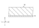
- FIG. 3 is a sectional view of a part of the wafer shown in FIG. 2.
- It is a functional block diagram of a control device. It is explanatory drawing for demonstrating formation of the modified area
- FIG. 6 is an explanatory diagram for explaining a calculation of a positional deviation between a theoretical value and a measured value of a formation position of a correction reforming region inside a wafer by a calculation unit. It is an explanatory view for explaining amendment of positional relation information by an amendment part. It is a flowchart which shows the flow of a laser processing process of the wafer by a laser processing apparatus, especially the correction process of positional relationship information. It is explanatory drawing for demonstrating the laser processing of the wafer by the laser processing apparatus of 2nd Embodiment.
- FIG. 1 is a schematic diagram of a laser processing apparatus 10 according to the first embodiment.
- the laser processing apparatus 10 performs laser processing on the wafer 12 as a pre-process before dividing the wafer 12 (for example, a silicon wafer) into a plurality of chips 14 (see FIG. 2).
- the XYZ directions in the drawing are orthogonal to each other, of which the X direction and the Y direction are horizontal directions, and the Z direction is the vertical direction (thickness direction of the wafer 12).
- the ⁇ direction is a rotation direction with the Z direction as the rotation axis.
- FIG. 2 is a plan view of the wafer 12 to be processed by the laser processing apparatus 10.
- FIG. 3 is a sectional view of a part of the wafer 12 shown in FIG. As shown in FIGS. 2 and 3, the wafer 12 is divided into a plurality of regions by a plurality of streets 12S (see FIG. 10) arranged in a grid. A device layer 16 that constitutes the chip 14 is provided in each of these partitioned regions.
- the laser processing apparatus 10 forms the modified region 200 (see FIG. 6) inside the wafer 12 along the plurality of planned dividing lines C1 and C2 set on the street 12S.
- the planned division line C1 and the planned division line C2 are orthogonal to each other.
- the laser processing device 10 includes an X ⁇ stage 20, a processing unit 22, and a control device 24.
- the X ⁇ stage 20 adsorbs and holds the surface (front surface) of the wafer 12 on the side where the device layer 16 is provided via a protective tape (not shown).
- the wafer 12 is held by the X ⁇ stage 20 so that the back surface on the opposite side of the front surface of the wafer 12 faces a processing unit 22 described later. Therefore, the back surface of the wafer 12 corresponds to one surface of the present invention, and the front surface of the wafer 12 corresponds to the other surface of the present invention.
- the X ⁇ stage 20 is moved in the X direction and rotated in the ⁇ direction by the stage drive mechanism 26 (see FIG. 4) under the control of the control device 24 described later.
- the stage drive mechanism 26 has a configuration in which a known linear movement mechanism and rotation mechanism are combined. Further, the moving direction M1 is the moving direction of the X ⁇ stage 20 toward one side in the X direction, and the moving direction M2 is the moving direction of the X ⁇ stage 20 toward the other side in the X direction.
- the processing unit 22 includes a laser unit 28 and an infrared microscope 30.
- the processing unit 22 is arranged on the upper side in the Z direction of the X ⁇ stage 20, and is controlled by the control device 24 described later.
- the processing unit 22 is moved in the Y direction and the Z direction by the unit drive mechanism 32 (see FIG. 4) under the control of the control device 24 described later.
- the unit drive mechanism 32 constitutes the relative movement mechanism of the present invention together with the stage drive mechanism 26 described above, and a known linear movement mechanism is used.
- the laser unit 28 corresponds to the laser optical system of the present invention, and irradiates the back surface of the wafer 12 with the laser light L.
- the laser unit 28 includes a laser light source 40, a beam expander 42, a mirror 44, a ⁇ / 2 wavelength plate 46, a spatial light modulator 48, a mirror 50, a mirror 52, a lens 54, a mirror 56, a mirror 58, a lens 60, and a collector.
- An optical lens 62 is provided.
- the configuration of the laser unit 28 is not limited to the configuration shown in FIG. 1, and various head configurations used for laser processing the wafer 12 may be adopted.
- the laser light source 40 emits laser light L for laser processing of the wafer 12 toward the beam expander 42. Since the type of the laser light L is a known technique (see, for example, Patent Document 1), a specific description will be omitted here.
- the beam expander 42 expands the laser light L incident from the laser light source 40 into an appropriate beam diameter for phase modulation by the spatial light modulator 48 described later.
- the laser light L emitted from the beam expander 42 enters the spatial light modulator 48 via the mirror 44 and the ⁇ / 2 wavelength plate 46.
- the spatial light modulator 48 for example, a reflective liquid crystal (LCOS: Liquid Crystal on Silicon) spatial light modulator (SLM: Spatial Light Modulator) is used.
- the spatial light modulator 48 modulates the laser light L incident from the ⁇ / 2 wavelength plate 46 by presenting a predetermined hologram pattern under the control of the control device 24.
- the laser light L is aberration-corrected so that the aberration of the laser light L focused inside the wafer 12 becomes equal to or less than the predetermined aberration. Since the configuration and function of the spatial light modulator 48 is a known technique (see Patent Document 1 above), a detailed description thereof will be omitted here.
- the laser light L modulated by the spatial light modulator 48 passes through the mirror 50, the mirror 52, the lens 54, the mirror 56, the mirror 58, and the lens 60, and is condensed by the condenser lens 62.
- the position of the condenser lens 62 is adjusted in the Z direction by a lens moving mechanism (not shown). Under the control of the control device 24, this lens moving mechanism adjusts the Z-direction position of the condensing point of the laser light L by adjusting the Z-direction position of the condensing lens 62.
- the optical axis A1 of the condenser lens 62 corresponds to the first optical axis of the present invention.
- the infrared microscope 30 corresponds to the infrared photographing optical system of the present invention.
- the infrared microscope 30 is fixed to the laser unit 28 and moves integrally with the laser unit 28.
- the infrared microscope 30 includes an illumination light source 64, a half mirror 66, an objective lens 68, an infrared camera 70, and the like.
- the illumination light source 64 is an epi-illumination light source, and for example, an LD (Laser Diode) light source and an SLD (Super Luminescent Diode) light source are used.
- the illumination light source 64 outputs illumination light in the wavelength range that passes through the wafer 12, for example, infrared light in the infrared range, toward the half mirror 66.
- the half mirror 66 transmits a part of the illumination light incident from the illumination light source 64 and emits it toward the objective lens 68.
- the illumination light is condensed on the back surface of the wafer 12 by the objective lens 68.
- the Z-direction position of the condensing point of the illumination light condensed by the objective lens 68 is adjusted by moving the objective lens 68 in the Z direction by a lens moving mechanism (not shown).
- the optical axis A2 of the objective lens 68 is the optical axis A2 of the infrared microscope 30 [the illumination axis of the illumination light source 64 and the photographing optical axis of the infrared camera 70 described later], and corresponds to the second optical axis of the present invention.
- the optical axes A1 and A2 are both parallel to the Z direction.
- a part of the reflected light of the illumination light reflected by the wafer 12 is reflected by the half mirror 66 toward the infrared camera 70.
- the infrared camera 70 includes an image sensor (not shown) having sensitivity to the wavelength range of infrared light.
- the internal state of the wafer 12 can be confirmed based on the captured image of the wafer 12 captured by the infrared camera 70 in a state where the objective lens 68 focuses the inside of the wafer 12. Further, the state of the back surface or the front surface of the wafer 12 can be confirmed based on the captured image of the wafer 12 taken by the infrared camera 70 in a state where the back surface or the front surface of the wafer 12 is focused by the objective lens 68.
- Image data of a captured image captured by the infrared camera 70 is output to the control device 24.
- the control device 24 causes the monitor 72 to display the captured image of the inside, the back surface, or the front surface of the wafer 12 based on the image data of the captured image input from the infrared camera 70.
- the infrared camera 70 for example, a camera (near infrared camera) having high sensitivity in the near infrared region (wavelength region of 1 ⁇ m or more) represented by an InGaAs (indium gallium arsenide) camera is preferably used.
- a camera near infrared camera having high sensitivity in the near infrared region (wavelength region of 1 ⁇ m or more) represented by an InGaAs (indium gallium arsenide) camera is preferably used.
- the optical axis A2 of the infrared microscope 30 is located downstream of the position of the optical axis A1 of the laser unit 28 described above in the moving direction M1 (one direction of the X direction) of the wafer 12 during laser processing. As a result, the infrared microscope 30 can photograph the wafer 12 on the planned dividing lines C1 and C2 at the same processing position of the wafer 12 by the laser light L of the laser unit 28.
- FIG. 4 is a functional block diagram of the control device 24.
- the control device 24 includes a stage drive mechanism 26, a laser unit 28 (laser light source 40 and spatial light modulator 48), an infrared microscope 30 (illumination light source 64 and infrared camera 70), and a unit.
- the drive mechanism 32, the monitor 72, and the operation unit 74 are connected to each other.
- As the operation unit 74 a known keyboard, mouse, operation button, and the like are used.
- the control device 24 is composed of an arithmetic device such as a personal computer, for example, and includes an arithmetic circuit composed of various processors and memories.
- CPUs Central Processing Units
- GPUs Graphics Processing Units
- ASICs Application Specific Integrated Circuits
- programmable logic devices eg, SPLDs (Simple Programmable Logic Devices), CPLDs (Complex Programmable Logic Devices), And FPGA (Field Programmable Gate Arrays)] and the like.
- the various functions of the control device 24 may be realized by one processor or a plurality of processors of the same type or different types.
- the control device 24 functions as an overall control unit 80, a storage unit 82, a movement control unit 84, a laser control unit 86, a microscope control unit 88, and a display control unit 90 by executing a control program (not shown).
- a control program not shown.
- what is described as “-unit” in the present embodiment may be “-circuit”, “-device”, or “-device”. That is, what is described as “-unit” may be configured by any of firmware, software, hardware, or a combination thereof.
- the integrated control unit 80 comprehensively controls the operation of each unit of the laser processing apparatus 10 based on the input operation to the operation unit 74.
- positional relationship information 92 is stored in advance in addition to the above control program.
- the positional relationship information 92 is known information indicating a relative positional relationship between the position of the optical axis A1 of the laser unit 28 (XY coordinates) and the position of the optical axis A2 of the infrared camera 70 (XY coordinates) in the XY directions.
- a value measured by the manufacturer of the laser processing apparatus 10 is stored.
- the positional relationship information 92 is corrected (rewritten) by the correction unit 116 described later.
- the movement control unit 84 drives the stage drive mechanism 26 and the unit drive mechanism 32 under the control of the overall control unit 80, respectively, so that the laser unit 28 and the infrared microscope 30 are integrated into the XYZ directions and ⁇ with respect to the wafer 12. Move relative to each other. As a result, the optical axis A1 of the laser unit 28 is aligned with the processing start position of the wafer 12 (one end of the planned dividing lines C1, C2) before the laser processing, or the laser unit 28 is moved relative to the wafer 12 at the time of the laser processing. It can be moved relative to each other. Further, before laser processing, the optical axis A2 of the infrared microscope 30 can be aligned with a specific position of the wafer 12 [alignment reference, and a modified region for correction 200 (see FIG. 6) described later, etc.].
- the laser control unit 86 controls the emission of the laser light L by the laser light source 40 and the modulation of the laser light L by the spatial light modulator 48. Since the modulation control of the laser light L by the spatial light modulator 48 is a known technique, a detailed description thereof will be omitted.
- the microscope control unit 88 controls the infrared microscope 30, that is, the emission of the illumination light by the illumination light source 64 and the imaging of the wafer 12 by the infrared camera 70.
- the display control unit 90 controls the display on the monitor 72.
- the display control unit 90 displays the captured image on the monitor 72 based on the image data of the captured image of the wafer 12 input from the infrared camera 70 of the infrared microscope 30.
- the display controller 90 also causes the monitor 72 to display various setting screens of the laser processing apparatus 10.
- the integrated control unit 80 functions as the detection control unit 96, the laser processing control unit 98, the imaging control unit 112, the calculation unit 114, and the correction unit 116 by executing the control program described above.
- the detection control unit 96 controls each unit of the laser processing apparatus 10 to detect the positions (including the orientation in the XY plane) of the planned dividing lines C1 and C2 of the wafer 12 held on the X ⁇ stage 20. Perform detection.
- the detection control unit 96 controls the stage drive mechanism 26, the unit drive mechanism 32, and the infrared microscope 30 via the movement control unit 84 and the microscope control unit 88, and the captured image 102 of the alignment reference of the wafer 12 is captured.
- Acquire (capture) image data is a reference for the laser processing apparatus 10 to recognize the positions of the dividing lines C1 and C2 of the wafer 12, and for example, the street 12S (see FIG. 10) and the recognition mark (not shown). The known standard of is used. It should be noted that the alignment reference may be provided at any position such as the inside, front surface, and back surface of the wafer 12 as long as it can be photographed by the infrared microscope 30.
- the detection control unit 96 drives the stage drive mechanism 26 and the unit drive mechanism 32 to cause the infrared microscope 30 to capture an image at the alignment reference of the wafer 12. [Alignment reference is moved to a position included in the imaging range VA of the infrared microscope 30 (see FIG. 9)]. After this movement, the detection control unit 96 controls the infrared microscope 30 to cause the infrared microscope 30 to execute the imaging of the wafer 12 including the alignment reference. As a result, the infrared microscope 30 acquires image data of the captured image 102 of the wafer 12, and the image data is output from the infrared microscope 30 to the detection control unit 96.
- the captured image 102 corresponds to the first captured image of the present invention.
- the detection control unit 96 detects the positions of the dividing lines C1 and C2 of the wafer 12 by detecting the alignment reference in the captured image 102 by a known image recognition method based on the image data of the captured image 102. ..
- the laser processing control unit 98 controls the stage drive mechanism 26, the unit drive mechanism 32, and the laser unit 28 via the movement control unit 84 and the laser control unit 86, and divides the planned division lines C1 and C2. Laser processing is performed to form the modified region 200 (see FIG. 6) inside the wafer 12 along the lines C1 and C2.
- the laser processing control unit 98 drives the stage drive mechanism 26 via the movement control unit 84 to rotate the X ⁇ stage 20 in the ⁇ direction based on the alignment detection result by the detection control unit 96, thereby mutually
- One of the orthogonal planned dividing lines C1 and C2 (for example, the planned dividing line C1) is made parallel to the X direction.
- the laser processing control unit 98 starts forming the modified region 200 (see FIG. 6) corresponding to the first planned dividing line C1 among the plurality of planned dividing lines C1 parallel to the X direction.
- the laser processing control unit 98 divides the laser unit 28 (optical axis A1) based on the alignment detection result (position detection result of the planned division line C1) by the detection control unit 96 and the positional relationship information 92 in the storage unit 82. The relative positional relationship with the planned line C1 is determined.
- the laser processing control unit 98 can determine the relative positional relationship between the laser unit 28 (optical axis A1) and the planned dividing lines C1 and C2 based on the alignment detection result and the positional relationship information 92.
- the laser processing control unit 98 drives the stage drive mechanism 26 and the unit drive mechanism 32 via the movement control unit 84 based on the alignment detection result and the positional relationship information 92 to set the optical axis A1 of the laser unit 28. Alignment is performed to align with one end of the first planned dividing line C1, for example, one end on the moving direction M2 side.
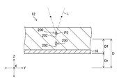
- 5 and 6 are explanatory diagrams for explaining formation of the modified region 200 inside the wafer 12.
- the laser processing control unit 98 controls the laser unit 28 after completion of the above-described alignment to focus the laser light L on the back surface of the wafer 12 at a predetermined depth position.
- the modified region 200 is formed at the position of this condensing point P1.
- the laser processing control unit 98 drives the stage drive mechanism 26 via the movement control unit 84 to move the X ⁇ stage 20 in the movement direction M2.
- the laser unit 28 is relatively moved in the moving direction M1 with respect to the wafer 12 in a state where the laser light L is focused on the focusing point P1, that is, the laser is moved along the first planned dividing line C1.
- the unit 28 is moved relative to the wafer 12 in the X direction.
- the modified region 200 is formed inside the wafer 12 along the first division line C1. Further, when the modified region 200 is formed, a crack 202 is generated in the thickness direction (Z direction) of the wafer 12 starting from the modified region 200.
- the laser processing control unit 98 forms the modified region 200 near the surface of the wafer 12 in the Z direction (thickness direction of the wafer 12).
- the vicinity of the surface of the wafer 12 referred to here is a focusing range D of the infrared microscope 30 in a state of being focused on the surface of the wafer 12 in the Z direction (within one side range Df of the focusing range D on the wafer 12 side).
- Reference numeral Dr in the figure is one side of the focusing range D on the side opposite to the wafer 12 side.
- the defocus allowable value a is obtained by performing image processing (recognition) on the image of the modified region 200 in the captured image 122 described later even when the modified region 200 is out of the range of the front depth of field. ) It is possible range.
- the laser processing control unit 98 drives the unit through the movement control unit 84 after forming the modified region 200 corresponding to the first planned dividing line C1.
- the mechanism 32 is driven to move the laser unit 28 in the Y direction toward the second planned dividing line C1 by a distance corresponding to the pitch interval of the planned dividing line C1.
- alignment is performed in which the optical axis A1 of the laser unit 28 is aligned with one end of the second planned dividing line C1, for example, one end on the moving direction M1 side.
- the laser processing control unit 98 controls the stage drive mechanism 26 and the laser unit 28 via the movement control unit 84 and the laser control unit 86 to focus the laser light L of the laser unit 28 on the focusing point P1.
- X ⁇ stage 20 is moved in the moving direction M1.
- the modified region 200 is formed inside the wafer 12 along the second planned dividing line C1.
- the modified region 200 is formed inside the wafer 12 along all the planned dividing lines C1.
- the laser processing control unit 98 drives the stage drive mechanism 26 via the movement control unit 84 to rotate the X ⁇ stage 20 by 90 °, thereby making the planned division line C2 parallel to the X direction.
- the laser processing control unit 98 similarly to the formation of the modified region 200 corresponding to the planned division line C1, via the movement control unit 84 and the laser control unit 86, the stage drive mechanism 26, the unit drive mechanism 32, and the laser.
- the unit 28 is controlled to form the modified region 200 inside the wafer 12 along all the planned dividing lines C2. This completes the formation of the modified region 200.
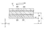
- FIGS. 7 and 8 are explanatory views for explaining formation of the two-layer modified region 200 inside the wafer 12.
- the laser processing control unit 98 forms the modified region 200 of, for example, two layers inside the wafer 12 along the dividing lines C1 and C2. To do. In this case, the laser processing control unit 98 continuously forms the two-layer modified region 200 for each of the planned dividing lines C1 and C2.
- the laser processing control unit 98 forms the modified region 200 of the first layer corresponding to the first planned dividing line C1 as described with reference to FIGS.
- the modified region 200 of the second layer Formation is repeated.
- a two-layer modified region 200 is formed inside the wafer 12 along the first planned dividing line C1.
- the second layer The modified region 200 is formed outside the one-sided range Df, that is, outside the focusing range D of the infrared microscope 30 in a state where the surface of the wafer 12 is focused.
- the laser processing of the modified region 200 of the first layer corresponding to the first planned dividing lines C1 and C2 is performed by photographing the captured image 122 by the infrared microscope 30 described later (the laser of the modified region 200 of the second layer is processed).
- the modified region 200 of the second layer may be formed within the focus range D.
- the laser processing control unit 98 similarly forms the modified region 200 of the second layer for each of the other planned dividing lines C1 and C2.
- the modified region 200 may be formed of three or more layers by repeating laser processing a plurality of times depending on the thickness of the wafer 12.
- the number of layers of the modified region 200 for each of the planned division lines C1 and C2 is two.
- the first modified region 200 corresponds to the first modified region of the present invention
- the second modified region 200 corresponds to the second modified region of the present invention.
- the imaging control unit 112, the calculation unit 114, and the correction unit 116 correct the positional relationship information 92 in the storage unit 82.
- the optical axis A1 of the laser unit 28 and the infrared camera are changed by changing the environment such as the room temperature of the factory (clean room) in which the laser processing device 10 is installed or changing the environment with time.
- the relative position of 70 with the optical axis A2 may shift.
- a deviation occurs between the positional relationship between the optical axis A1 and the optical axis A2 defined by the positional relationship information 92 and the actual positional relationship between the two.
- the optical axis A1 of the laser unit 28 is divided based on the initial (at the time of shipment) positional relationship information 92. Can not be aligned exactly on top. As a result, the processing accuracy of laser processing is reduced.
- the positional relationship information 92 of the positional relationship information 92 is based on the formation position of the first-layer reformed region 200 (hereinafter, referred to as the correction reformed region 200) corresponding to the first planned division lines C1 and C2.
- Make corrections updates.
- the positional relationship between the optical axis A1 of the laser unit 28 and the optical axis A2 of the infrared camera 70 shifts not only in the Y direction but also in the X direction, but the positional relationship between the optical axis A1 and the optical axis A2 in the X direction is different. The deviation hardly affects the processing accuracy of the laser processing of the wafer 12 along the planned dividing lines C1 and C2.
- a shift in the positional relationship between the optical axis A1 and the optical axis A2 in the Y direction is detected based on the formation position of the modified reforming region 200 described above, and the Y direction is detected based on the detection result of this shift.
- the positional relationship information 92 is corrected (updated).
- FIG. 9 is an explanatory diagram for explaining photographing control of the infrared microscope 30 by the photographing control unit 112.
- the photographing control unit 112 controls the photographing of the photographed image 122 by the infrared microscope 30.
- the imaging control unit 112 performs laser processing on the first layer modified region 200 (correction modified region 200) corresponding to the first planned dividing line C1 (before laser processing on the second layer modified region 200). ), Or after laser processing of the modified region 200 of the second layer.
- the imaging control unit 112 drives the stage drive mechanism 26 and the unit drive mechanism 32 via the movement control unit 84 based on the position detection result of the first planned dividing line C1 by the detection control unit 96 to move the wafer 12
- the first planned division line C1 is relatively moved within the imaging range VA of the infrared microscope 30.
- the imaging control unit 112 controls the infrared microscope 30 so that the infrared microscope 30 focuses on the surface of the wafer 12 and the first scheduled dividing line C1 (street 12S: see FIG. 10) by the infrared microscope 30.
- the photographed image 122 is photographed.
- the captured image 122 corresponds to the second captured image of the present invention.
- the photographing control unit 112 causes the infrared microscope 30 to photograph the photographed image 122 of the first planned division line C2 (street 12S) after laser processing corresponding to the first planned division line C2. ..
- the infrared microscope 30 In order to focus the infrared microscope 30 on the surface of the wafer 12, it is also possible to focus the infrared microscope 30 on the tape surface of a protective tape (not shown) that is in close contact with the surface of the wafer 12. included. Then, the infrared microscope 30 can be easily focused on the surface of the wafer 12 by targeting scratches, foreign matters, patterns, or the like on the tape surface of the protective tape. Further, the method of focusing the infrared microscope 30 on the surface of the wafer 12 (on the side opposite to the surface facing the infrared microscope 30) is not limited to the above-mentioned method, and various known methods may be used.
- the infrared microscope 30 executes the imaging of the first planned division lines C1 and C2, the infrared microscope 30 instructs the calculation unit 114 of the captured images 122 of the planned division lines C1 and C2. Image data is output.
- the modified region 200 of the first layer for each of the planned dividing lines C1 and C2 is an infrared microscope in a state where the surface of the wafer 12 is focused, as shown in FIGS. It is formed within one side range Df of 30 (within the focusing range D). For this reason, the infrared microscope 30 performs the image capturing while focusing on the surface of the wafer 12, and at the same time, the image is captured with the modified modified region 200 included in the focusing range D. As a result, since the correction modification area 200 included in the captured image 122 is in focus, the correction modification area 200 in the captured image 122 can be recognized (identified).
- the first planned dividing lines C1 and C2 are relatively moved within the imaging range VA of the infrared microscope 30 and then the infrared microscope 30 is focused on the surface of the wafer 12. After the focus of the infrared microscope 30 is adjusted to the surface of the wafer 12, the first division lines C1 and C2 may be relatively moved within the imaging range VA.
- FIG. 10 is an explanatory diagram for explaining the calculation of the positional deviation between the theoretical value and the actually measured value of the formation position of the correction reforming region 200 inside the wafer 12 by the calculation unit 114.
- the calculation unit 114 detects the modified region for correction 200 (displayed with diagonal lines) in the captured image 122 by a known image recognition method based on the image data of the captured image 122.
- the photographed image 122 is being photographed by the infrared microscope 30 after the laser processing of the modified region 200 of the first layer corresponding to the first planned dividing line C1
- the photographed image 122 is Since the modified region 200 of the second layer does not exist, the modified region 200 of the second layer and the crack 202 are prevented from affecting the detection of the modified region for correction 200.
- the captured image 122 is taken by the infrared microscope 30 after the laser processing of the modified region 200 of the second layer, the modification of the second layer formed above the modified region 200 for correction is performed. Since the quality region 200 is formed outside the focusing range D of the infrared microscope 30, it is possible to prevent the modified region 200 and the crack 202 in the second layer from affecting the detection of the modified region for correction 200. To be done.
- the calculation unit 114 corrects the inside of the wafer 12 based on the position of the modified region for correction 200 in the captured image 122 and the position of the optical axis A2 of the infrared camera 70 at the time of capturing the captured image 122.
- the actual measurement value of the formation position of the modified region 200 in the Y direction is detected.
- the calculation unit 114 uses the detection result of the position of the first planned division lines C1 and C2 in the Y direction by the detection control unit 96 as a theory of the formation position of the correction reforming region 200 in the wafer 12 in the Y direction. Used as a value. This theoretical value shifts between the positional relationship (Y direction) between the optical axis A1 of the laser unit 28 and the optical axis A2 of the infrared camera 70, which is defined by the positional relationship information 92, and the actual positional relationship between both. It is the formation position of the modified reforming region 200 when it is assumed that there is not.
- the calculation unit 114 calculates ( ⁇ y) as a value indicating the positional deviation (the positional deviation amount and the deviation direction) in the Y direction between the theoretical value and the actual measurement value of the formation position of the correction reforming region 200. It should be noted that the magnitude of the value of ( ⁇ y) indicates the shift amount of the positional shift in the Y direction, and the positive / negative of the value of ( ⁇ y) indicates the shift direction of the positional shift (positive / negative in the Y direction).
- the positional deviation calculation result ( ⁇ y) is obtained by comparing the positional relationship between the optical axis A1 of the laser unit 28 and the optical axis A2 of the infrared camera 70 in the Y direction, which is determined by the positional relationship information 92, and the actual Y direction. It is zero when there is no deviation from the positional relationship. Therefore, the calculation result ( ⁇ y) is a value indicating how much the positional relationship between the optical axis A1 and the optical axis A2 changes from the design value in the Y direction.
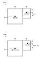
- FIG. 11 is an explanatory diagram for explaining correction of the positional relationship information 92 by the correction unit 116.
- coordinates (X1, Y1) are coordinates (design value) of the optical axis A2 of the infrared camera 70
- coordinates (X2, Y2) are coordinates (design value) of the optical axis A1 of the laser unit 28.
- the coordinates (X1, Y1) and the coordinates (X2, Y2) are relative position coordinates of the other [for example, the coordinates (X2, Y2)] based on one of the both [for example, the coordinates (X1, Y1)]. is there.
- Y1 Y2.
- the relative positional relationship between the optical axis A1 and the optical axis A2 is calculated from the positional relationship indicated by the positional relationship information 92 at the time of factory shipment as shown by reference symbol XIA in FIG.
- the positional relationship is changed to that shown by reference numeral XIB in FIG.
- the correction unit 116 calculates the actual (latest) position of the optical axis A1 of the laser unit 28 and the position of the optical axis A2 of the infrared camera 70 in the Y direction based on the calculation result ( ⁇ y) of the positional shift by the calculation unit 114.
- the relative positional relationship 92 in the storage unit 82 is corrected by calculating the relative positional relationship.
- the laser processing control unit 98 described above based on the position detection result of the detection control unit 96 and the positional relationship information 92 corrected by the correction unit 116, the laser unit 28, the stage drive mechanism 26, and the unit drive.
- the modified region 200 can be formed inside the wafer 12 along the second planned dividing lines C1 and C2.
- the correction of the positional relationship information 92 that is, the operation of each unit (the imaging control unit 112, the calculation unit 114, and the correction unit 116) is performed under the control of the overall control unit 80 for each direction of the planned division lines C1 and C2. It is executed at the timing of at least one of the wafers 12 and the plurality of wafers 12. Therefore, the overall control unit 80 functions as the repetition control unit of the present invention.
- the positional relationship information 92 may be corrected regularly or when the laser processing apparatus 10 is started.
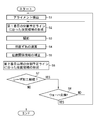
- FIG. 12 is a flowchart showing a flow of laser processing of the wafer 12 by the laser processing apparatus 10 of the first embodiment having the above-described configuration, particularly correction processing of the positional relationship information 92 corresponding to the control method of the laser processing apparatus of the present invention. is there.
- the detection control unit 96 of the control device 24 operates.
- the detection control unit 96 controls the stage drive mechanism 26, the unit drive mechanism 32, and the infrared microscope 30 to acquire image data of the alignment reference photographed image 102 of the wafer 12.
- the detection control unit 96 performs alignment detection for detecting the positions of the planned dividing lines C1 and C2 in the wafer 12 based on the image data of the captured image 102 (step S1, corresponding to the detecting step of the present invention).
- the laser processing control unit 98 When the alignment detection is completed, the laser processing control unit 98 operates.
- the laser processing control unit 98 based on the position detection result of the planned dividing lines C1 and C2 by the detection control unit 96 and the positional relationship information 92 in the storage unit 82, the stage drive mechanism 26, the unit drive mechanism 32, and the laser unit 28. And are driven to perform laser processing.
- the first-layer modified region 200 is formed inside the wafer 12 along the first planned dividing line C1 (step S2, which corresponds to the laser processing step of the present invention).
- the above-described laser processing causes the first-layer modified region 200 (correction-modified region 200) to be focused on the surface of the wafer 12 in the Z direction in the focusing range D of the infrared microscope 30. It is formed in (one side range Df).
- the imaging control unit 112 drives the stage drive mechanism 26 and the unit drive mechanism 32 based on the position detection result of the planned division lines C1 and C2 by the detection control unit 96 to drive the first planned division line C1 (street 12S). ) Is moved within the photographing range VA of the infrared microscope 30, and the infrared microscope 30 is focused on the surface of the wafer 12. Then, the image capturing control unit 112 causes the infrared microscope 30 to perform image capturing of the first planned division line C1 (step S3, which corresponds to the image capturing step of the present invention). As a result, the infrared microscope 30 outputs the image data of the captured image 122 to the calculation unit 114.
- the laser processing control unit 98 is activated again to drive the stage drive mechanism 26, the unit drive mechanism 32, and the laser unit 28 to perform laser processing.
- the modified region 200 of the second layer is formed inside the wafer 12 along the first planned dividing line C1.
- the step S3 may be executed after the laser processing of the modified region 200 of the second layer.
- the modified region 200 of the second layer is formed outside the focusing range D in the Z direction.
- the calculation unit 114 operates in response to input of image data of the captured image 122 from the infrared microscope 30.
- the calculation unit 114 detects the correction modification area 200 in the captured image 122 based on the image data of the captured image 122 by the image recognition method.
- the correction modification region 200 is formed in the focusing range D (within the one-sided range Df) of the infrared microscope 30 in the state where the surface of the wafer 12 is focused, so the calculation unit 114 causes the captured image.
- the modified reformed region 200 in 122 can be detected.
- step S3 when step S3 is performed before the laser processing of the modified region 200 of the second layer, the modified region 200 and the crack 202 of the second layer are included in the captured image 122 in the captured image 122. Is prevented. Even when step S3 is performed after laser processing of the modified region 200 of the second layer, the modified region 200 of the second layer is formed outside the focusing range D of the infrared microscope 30. There is. Therefore, in any case, it is possible to prevent the second modified region 200 and the crack 202 from affecting the detection of the modified modified region 200 by the calculation unit 114.
- the calculation unit 114 performs the correction in the wafer 12 based on the position of the modified region for correction 200 in the captured image 122 and the position of the optical axis A2 of the infrared microscope 30 at the time of capturing the captured image 122.
- the actual measurement value of the formation position of the modified area for use 200 is detected.
- the calculation unit 114 acquires the position detection result of the first planned division line C1 detected by the detection control unit 96 at the time of alignment detection as a theoretical value of the formation position of the modified reforming region 200 in the wafer 12. To do. Then, as shown in FIG.
- the calculation unit 114 calculates the position deviation in the Y direction between the theoretical value and the actual measurement value of the correction reforming region 200, and the calculation result ( ⁇ y) is calculated by the correction unit.
- Output to 116 step S4, which corresponds to the calculation process of the present invention).
- step S5 which corresponds to the correction step of the present invention.
- the laser processing control unit 98 When the correction of the positional relationship information 92 is completed, the laser processing control unit 98 operates again.
- the laser processing control unit 98 drives the stage drive mechanism 26, the unit drive mechanism 32, and the laser unit 28 based on the alignment detection result by the detection control unit 96 and the corrected positional relationship information 92 in the storage unit 82.
- the two-layer modified region 200 is formed inside the wafer 12 along the planned dividing line C1 before the laser processing (second or later) ( Step S6). Note that step S6 also corresponds to the laser processing step of the present invention.
- the laser processing of the wafer 12 is performed based on the corrected positional relationship information 92, the relative position between the optical axis A1 of the laser unit 28 and the optical axis A2 of the infrared camera 70 due to changes in the environment in which the laser processing apparatus 10 is installed. Even if is deviated from the design value, the modified region 200 can be formed inside the wafer 12 with high accuracy along the second and subsequent division lines C1.
- the integrated control unit 80 executes repetitive control for repeatedly operating the laser processing control unit 98, the imaging control unit 112, the calculation unit 114, and the correction unit 116 after forming the modified region 200 along each planned division line C1. (YES in step S7, NO in step S8). As a result, the above-described processing from step S2 to step S6 is repeatedly executed. That is, formation of the modified region 200 inside the wafer 12 along the first planned dividing line C2, imaging of the first planned dividing line C2, calculation of positional deviation, and re-creation of the positional relationship information 92. The correction and the formation of the modified region 200 corresponding to the second and subsequent planned dividing lines C2 are executed. With the above, laser processing of one wafer 12 is completed.
- step S1 to step S7 is repeatedly executed (YES in step S7, YES in step S8).
- the processes from step S3 to step S5 may be executed for each of the plurality of wafers 12.
- the wafer 12 after laser processing is divided into a plurality of chips 14 by a known dividing device.
- the laser processing apparatus 10 forms the correction modification region 200 inside the wafer 12, captures the captured image 122 by the infrared microscope 30, and the formation position of the correction modification region 200.
- the positional relationship information 92 can be corrected by calculating the positional deviation between the theoretical value and the actually measured value. As a result, even if the relative position between the optical axis A1 of the laser unit 28 and the optical axis A2 of the infrared microscope 30 deviates from the design value due to changes in the environment in which the laser processing apparatus 10 is installed, this deviation is related to the positional relationship information. It can be reflected in 92.
- the modified region 200 can be formed inside the wafer 12 with high accuracy along the dividing lines C1 and C2 regardless of changes in the environment in which the laser processing apparatus 10 is installed. Further, since it is not necessary to prepare the processed sample piece or to attach / detach the processed sample piece to / from the X ⁇ stage 20 as in Patent Document 3, it is possible to reduce the labor and cost. As a result, highly accurate laser processing of the wafer 12 can be easily performed.
- [Second Embodiment] 13 and 14 are explanatory views for explaining the laser processing of the wafer 12 by the laser processing apparatus 10 according to the second embodiment.
- the laser processing apparatus 10 according to the second embodiment has basically the same configuration as the laser processing apparatus 10 according to the first embodiment, and therefore, the same reference numerals are used for the same functions or configurations as those of the first embodiment. Is attached and its description is omitted.
- the captured image 122 is captured by the infrared microscope 30.
- the method for forming the modified region 200 inside the wafer 12 along the first planned dividing line C1 is different from the method for forming the first embodiment. Different.
- the laser processing control unit 98 of the second embodiment controls the stage drive mechanism 26, the unit drive mechanism 32, and the laser unit 28 so that the wafer in the entire range of the first scheduled dividing line C1 is the same as in the above embodiment.
- a modified region 200 of the first layer is formed inside 12.
- the laser processing control unit 98 controls the stage drive mechanism 26, the unit drive mechanism 32, and the laser unit 28 so that the specific region 250 is excluded from the entire range of the first scheduled division line C1.
- a modified region 200 of the second layer is formed inside the wafer 12.
- the specific area 250 is, for example, an invalid area on the outer peripheral portion of the wafer 12.
- This ineffective region is a region in the wafer 12 that is separated from the chip 14 (a region that does not affect the quality of the chip 14).
- the imaging control unit 112 of the second embodiment drives the stage drive mechanism 26 and the unit drive mechanism 32 via the movement control unit 84 to move the specific area 250 relatively within the imaging range VA of the infrared microscope 30. Then, the image capturing control unit 112 controls the infrared microscope 30 to cause the infrared microscope 30 to capture the captured image 122 of the specific region 250 with the focus of the infrared microscope 30 on the surface of the wafer 12.
- the second modified region 200 is not formed above the correction modified region 200 (the first modified region 200) in the Z direction, that is, the correction modified region 200 and the infrared microscope 30 are combined.
- the modified region 200 and the crack 202 of the second layer are not formed between them.
- the computing unit 114 detects the correction modified region 200 in the captured image 122, it is possible to reliably prevent the influence of the modified region 200 of the second layer and the crack 202.
- the detection accuracy of the actual measurement value of the formation position of the correction reforming region 200 is improved, so that the positional relationship information 92 can be corrected with higher accuracy.
- the laser processing conditions of the first-layer modified region 200 (correction-modified region 200) in the specific region 250 are set to the first-layer modified region 200 outside the specific region 250. May be different from. Specifically, the laser processing condition of the first modified region 200 in the specific region 250 is set to a condition that improves the contrast of the corrected modified region 200 in the captured image 122 (for example, the modified correction region 200). The line width of the quality region 200 may be narrowed).
- [Third Embodiment] 15 and 16 are explanatory views for explaining laser processing of the wafer 12 by the laser processing apparatus 10 of the third embodiment.
- the laser processing apparatus 10 according to the third embodiment has basically the same configuration as the laser processing apparatus 10 according to the first embodiment. Therefore, the same reference numerals are used for the same functions or configurations as those of the first embodiment. Is attached and its description is omitted.
- the imaging position of the wafer 12 by the infrared microscope 30 is different from the imaging position of each of the above embodiments.
- a metal pattern 260 such as a TEG (Test Element Group) for testing the function of the device is formed on the surface of the wafer 12 (device layer 16).
- the imaging control unit 112 drives the stage drive mechanism 26 and the unit drive mechanism 32, and is a pattern that is a region in which the metal pattern 260 is formed in the first planned division lines C1 and C2.
- the formation area 262 is relatively moved within the imaging range VA of the infrared microscope 30.
- the photographing control unit 112 causes the infrared microscope 30 to photograph the photographed image 122 of the pattern formation region 262 with the focus of the infrared microscope 30 on the surface (metal pattern 260) of the wafer 12.
- the image data of the photographed image 122 of the pattern formation area 262 of the first planned dividing lines C1 and C2 is obtained.
- both the correction modification area 200 and the metal pattern 260 are in focus. Therefore, the background of the correction modification region 200 becomes the metal pattern 260, and thus the contrast of the correction modification region 200 can be improved under the epi-illumination by the infrared microscope 30. As a result, also in the third embodiment, the detection accuracy of the actual measurement value of the formation position of the correction reforming region 200 is improved, so that the positional relationship information 92 can be corrected with higher accuracy.
- FIG. 17 is an explanatory diagram for explaining a modified example of the processing unit 22.
- the position of the optical axis A1 of the laser unit 28 and the position of the optical axis A2 of the infrared camera 70 in the Y direction are aligned by design, but as shown by reference numeral XVIIA in FIG. , The position of the optical axis A1 of the laser unit 28 in the Y direction and the position of the optical axis A2 of the infrared camera 70 may be displaced.
- ⁇ y Y2-Y1.
- the calculation unit 114 does The actual relative positional relationship between the optical axis A1 and the optical axis A2 can be calculated based on the calculation result ( ⁇ y) of the positional deviation.
- the positional relationship information 92 in the storage unit 82 can be corrected as in the above embodiment.
- the positional deviation between the measured value and the theoretical value of the start end position and / or the end position in the X direction of the correction reforming region 200 is detected, and the positional relationship information 92 in the X direction is based on the detection result of this deviation.
- a specific method is basically the same as the detection of the positional deviation in the Y direction and the correction of the positional relationship information 92, and thus a specific description thereof will be omitted here.
- the first-layer modified region 200 corresponding to the first planned dividing lines C1 and C2 is used as the correction modified region 200, but any second and subsequent planned dividing lines C1 and C2 are used.
- the modified region 200 of the first layer corresponding to the above may be used as the modified region 200 for correction.
- stage drive mechanism 26 and the unit drive mechanism 32 are described as an example of the relative movement mechanism of the present invention.
- the configuration is not particularly limited.
- the infrared microscope 30 is connected to the outside of the laser unit 28, but the infrared microscope 30 may be provided inside the housing of the laser unit 28.
Landscapes
- Physics & Mathematics (AREA)
- Optics & Photonics (AREA)
- Engineering & Computer Science (AREA)
- Plasma & Fusion (AREA)
- Mechanical Engineering (AREA)
- Chemical & Material Sciences (AREA)
- Chemical Kinetics & Catalysis (AREA)
- General Chemical & Material Sciences (AREA)
- Oil, Petroleum & Natural Gas (AREA)
- Laser Beam Processing (AREA)
- Dicing (AREA)
Abstract
高精度なウェーハのレーザ加工を簡単に行うことができるレーザ加工装置及びその制御方法を提供する。ウェーハの複数の分割予定ラインの位置を検出する検出制御部と、検出制御部による分割予定ラインの位置検出結果と、第1光軸及び第2光軸の位置関係情報と、に基づき、レーザ加工を実行するレーザ加工制御部と、赤外線撮影光学系の焦点をウェーハの一面とは反対側の他面に合せた状態で赤外線撮影光学系による分割予定ラインの第2撮影画像の撮影を実行させる撮影制御部と、位置関係情報と第2撮影画像とに基づき、改質領域の形成位置の理論値と実測値との位置ずれを演算する演算部と、演算部の演算結果に基づき、位置関係情報を補正する補正部と、を備え、改質領域を、ウェーハの厚み方向において他面に焦点を合わせた状態の赤外線撮影光学系の合焦範囲内に形成する。
Description
本発明は、ウェーハの内部に集光点を合わせてレーザ光を照射することにより、ウェーハの分割予定ラインに沿ってウェーハの内部に改質領域を形成するレーザ加工装置及びその制御方法に関する。
表面に複数のデバイスが形成されたウェーハの内部に集光点を合わせてレーザ光を照射して、ウェーハの分割予定ラインに沿ってウェーハの内部に改質領域を形成するレーザ加工が知られている(特許文献1参照)。そして、レーザ加工後のウェーハは、外的応力の印加により、改質領域を起点として個々のチップに分割される。
このようなレーザ加工を行うレーザ加工装置として、ウェーハの一面に向けてレーザ光を照射するレーザユニット(レーザヘッドともいう)と、レーザユニットに固定され且つウェーハの一面を撮影する赤外線顕微鏡と、を備えるものが知られている(特許文献2参照)。このレーザ加工装置では、改質領域の形成前に、赤外線顕微鏡でウェーハのアライメント基準を撮影し、この撮影により得られた撮影画像に基づきウェーハの分割予定ラインの位置(赤外線顕微鏡に対する分割予定ラインの相対位置)を検出するアライメント検出を行う。
次いで、分割予定ラインの位置検出結果と、既知のレーザユニットの光軸及び赤外線顕微鏡の光軸の位置関係情報とに基づき、分割予定ラインの一端にレーザユニットの光軸を位置合わせするアライメントを行う。そして、レーザユニットからウェーハの内部の集光点に向けてレーザ光を照射させると共に、レーザユニット及びウェーハを相対移動させることで、分割予定ラインに沿ってウェーハの内部に改質領域を形成する。以下、分割予定ラインごとに、上述のアライメントと改質領域の形成とが繰り返し実行される。
特許文献3には、レーザユニットからウェーハに照射されるレーザ光の照射位置の目標値(理論値)と実測値との位置ずれを取得するレーザ加工装置が記載されている。このレーザ加工装置は、ウェーハを保持するウェーハステージとは別の試料載置ステージを備えている。そして、この試料載置ステージに加工試料片を載置した後、レーザユニットから加工試料片の表面にレーザ光を照射してレーザ加工痕跡を形成する。次いで、このレーザ加工痕跡を観察光学部で撮影し、この撮影により得られた撮影画像に基づき、レーザ光の照射位置の目標値と実測値との位置ずれを検出している。
ところで、特許文献2に記載のレーザ加工装置では、装置が設置されている工場(クリーンルーム)の室内温度等の環境が変わったり或いは環境が時間的に変化したりすることで、レーザユニットの光軸と赤外線顕微鏡の光軸との相対位置がずれる場合がある。この場合には、レーザユニットによるレーザ光の加工位置が分割予定ラインに対して位置ずれするため、精度の高い加工ができなくなる。このため、従来では、定期的なメンテナンスで位置ずれを補正するなど対策を実施しているが、工場によっては気温の変化が大きいため、短期間で位置ずれが発生するおそれがある。
このような位置ずれを防止するため、改質領域形成時にレーザ光の加工位置の補正を行うことが望ましいが、ウェーハの厚みによっては1つの分割予定ラインに対してレーザ光で複数回スキャンすることが必要になる。この場合、改質領域及び亀裂の蛇行が複数重なることにより、レーザ光の加工位置の補正が困難になる。そして、数μmの補正ずれが発生すると、例えば分割予定ラインの幅が20μm以下の狭ストリートプロセスにおいて大きく歩留まりを落とすことになる。
そこで、特許文献2に記載のレーザ加工装置においても、上記特許文献3に記載されているようにレーザユニットからウェーハに照射されるレーザ光の照射位置の目標値と実測値との位置ずれを検出することで、レーザユニットの光軸と赤外線顕微鏡の光軸との位置関係を取得することが考えられる。
しかしながら、特許文献3に記載の方法は、レーザユニットの光軸と赤外線顕微鏡の光軸とが一致しているレーザ加工装置を対象としているため、この特許文献3に記載の方法を特許文献2に記載のレーザ加工装置に単純に適用することはできない。また仮に適用することができたとしても、加工試料片を用意する手間及びコストと、加工試料片を試料載置ステージに着脱したりする手間及びコストと、が掛かるという問題がある。
本発明はこのような事情に鑑みてなされたものであり、高精度なウェーハのレーザ加工を簡単に行うことができるレーザ加工装置及びその制御方法を提供することを目的とする。
本発明の目的を達成するためのレーザ加工装置は、ウェーハの一面に向けてレーザ光を照射するレーザ光学系と、一面に対向する位置に配置され且つレーザ光学系の第1光軸とは異なる第2光軸を有し、ウェーハを撮影する赤外線撮影光学系と、レーザ光学系及び赤外線撮影光学系を一体にウェーハに対し相対移動させる相対移動機構と、を備えるレーザ加工装置であって、ウェーハの内部に対しレーザ光学系のレーザ光を集光させた状態で、相対移動機構によりウェーハの分割予定ラインに沿ってレーザ光学系をウェーハに対して相対移動させて、分割予定ラインに沿ってウェーハの内部に改質領域を形成するレーザ加工を行うレーザ加工装置において、赤外線撮影光学系にウェーハのアライメント基準を撮影させて、赤外線撮影光学系により撮影されたアライメント基準の第1撮影画像に基づき、ウェーハの複数の分割予定ラインの位置を検出する検出制御部と、検出制御部による分割予定ラインの位置検出結果と、第1光軸及び第2光軸の位置関係情報と、に基づき、レーザ光学系及び相対移動機構を駆動してレーザ加工を実行するレーザ加工制御部と、相対移動機構を駆動して赤外線撮影光学系の撮影範囲内に分割予定ラインを移動させ、且つ赤外線撮影光学系の焦点をウェーハの一面とは反対側の他面に合せた状態で赤外線撮影光学系による分割予定ラインの第2撮影画像の撮影を実行させる撮影制御部と、位置関係情報と第2撮影画像とに基づき、改質領域の形成位置の理論値と実測値との位置ずれを演算する演算部と、演算部の演算結果に基づき、位置関係情報を補正する補正部と、を備え、レーザ加工制御部が、改質領域を、ウェーハの厚み方向において他面に焦点を合わせた状態の赤外線撮影光学系の合焦範囲内に形成する。
このレーザ加工装置によれば、環境の変化等によりレーザ光学系の第1光軸と赤外線撮影光学系の第2光軸との相対位置が設計値からずれた場合であっても、レーザ光学系の第1光軸と赤外線撮影光学系の第2光軸との位置関係情報を補正することができる。
本発明の他の態様に係るレーザ加工装置において、補正部による位置関係情報の補正が行われた場合に、レーザ加工制御部が、検出制御部による分割予定ラインの位置検出結果と、補正部により補正された位置関係情報と、に基づき、レーザ加工前の分割予定ラインごとにレーザ加工を行う。これにより、分割予定ラインに沿って高精度にウェーハの内部に改質領域を形成することができる。
本発明の他の態様に係るレーザ加工装置において、レーザ加工制御部が、分割予定ラインごとに、複数回のレーザ加工であって且つ厚み方向におけるレーザ光の集光位置が互いに異なる複数回のレーザ加工を行い、分割予定ラインごとに複数層の改質領域を形成し、複数層の改質領域の中で最も他面側に位置する第1改質領域が、合焦範囲内に含まれている。これにより、演算部が第2撮影画像内の第1改質領域を認識することができる。
本発明の他の態様に係るレーザ加工装置において、複数層の改質領域の中で第1改質領域とは異なる改質領域を第2改質領域とした場合、レーザ加工制御部が、厚み方向において第2改質領域を合焦範囲の範囲外に形成する。これにより、第2改質領域が第1改質領域の検出に影響を及ぼすことが防止される。
本発明の他の態様に係るレーザ加工装置において、複数層の改質領域の中で第1改質領域とは異なる改質領域を第2改質領域とした場合、レーザ加工制御部が、分割予定ラインの全範囲で第1改質領域の形成を行い且つ全範囲の中でウェーハの外周部の特定領域を除いた範囲で第2改質領域の形成を行い、撮影制御部が、相対移動機構を駆動して赤外線撮影光学系の撮影範囲内に特定領域を移動させ、且つ赤外線撮影光学系の焦点を他面に合せた状態で赤外線撮影光学系による特定領域の撮影を実行させる。これにより、第1改質領域の形成位置の実測値の検出精度が向上するので、位置関係情報をより高精度に補正することができる。
本発明の他の態様に係るレーザ加工装置において、他面の分割予定ライン上に金属パターンが形成されており且つ分割予定ラインの中で金属パターンが形成されている領域をパターン形成領域とした場合、撮影制御部が、相対移動機構を駆動して赤外線撮影光学系の撮影範囲内にパターン形成領域を移動させ、且つ赤外線撮影光学系の焦点を他面に合せた状態で赤外線撮影光学系によるパターン形成領域の撮影を実行させる。これにより、改質領域のコントラストを向上させることができるので、改質領域の形成位置の実測値の検出精度が向上する。その結果、位置関係情報をより高精度に補正することができる。
本発明の他の態様に係るレーザ加工装置において、分割予定ラインの方向ごと、ウェーハごと、又は複数のウェーハごとに、少なくともレーザ加工制御部、撮影制御部、演算部、及び補正部を繰り返し作動させる繰り返し制御部を備える。これにより、所定のタイミングで位置関係情報を補正することができる。
本発明の他の態様に係るレーザ加工装置において、検出制御部が、相対移動機構を駆動して赤外線撮影光学系をアライメント基準の撮影位置に相対移動させ、且つ赤外線撮影光学系にアライメント基準を撮影させて、第1撮影画像を取得する。これにより、分割予定ラインの位置を検出することができる。
本発明の他の態様に係るレーザ加工装置において、赤外線撮影光学系が、第2光軸を照明軸としてウェーハを赤外光で照明する落射照明光源を備える。
本発明の目的を達成するためのレーザ加工装置の制御方法は、ウェーハの一面に向けてレーザ光を照射するレーザ光学系と、一面に対向する位置に配置され且つレーザ光学系の第1光軸とは異なる第2光軸を有し、ウェーハを撮影する赤外線撮影光学系と、レーザ光学系及び赤外線撮影光学系を一体にウェーハに対し相対移動させる相対移動機構と、を備えるレーザ加工装置であって、ウェーハの内部に対しレーザ光学系のレーザ光を集光させた状態で、相対移動機構によりウェーハの分割予定ラインに沿ってレーザ光学系をウェーハに対して相対移動させて、分割予定ラインに沿ってウェーハの内部に改質領域を形成するレーザ加工を行うレーザ加工装置の制御方法において、赤外線撮影光学系にウェーハのアライメント基準を撮影させて、赤外線撮影光学系により撮影されたアライメント基準の第1撮影画像に基づき、ウェーハの複数の分割予定ラインの位置を検出する検出工程と、検出工程での分割予定ラインの位置検出結果と、第1光軸及び第2光軸の位置関係情報と、に基づき、レーザ光学系及び相対移動機構を駆動してレーザ加工を実行するレーザ加工工程と、相対移動機構を駆動して赤外線撮影光学系の撮影範囲内に分割予定ラインを移動させ、且つ赤外線撮影光学系の焦点をウェーハの一面とは反対側の他面に合せた状態で赤外線撮影光学系による分割予定ラインの第2撮影画像の撮影を実行させる撮影工程と、位置関係情報と第2撮影画像とに基づき、改質領域の形成位置の理論値と実測値との位置ずれを演算する演算工程と、演算工程での演算結果に基づき、位置関係情報を補正する補正工程と、を有し、レーザ加工工程では、改質領域を、ウェーハの厚み方向において他面に焦点を合わせた状態の赤外線撮影光学系の合焦範囲内に含まれる位置に形成する。
本発明の他の態様に係るレーザ加工装置の制御方法は、補正工程で位置関係情報の補正が行われた場合に、レーザ加工工程では、検出工程での分割予定ラインの位置検出結果と、補正工程で補正された位置関係情報と、に基づき、レーザ加工前の分割予定ラインごとにレーザ加工を行う。
本発明は、高精度なウェーハのレーザ加工を簡単に行うことができる。
[第1実施形態のレーザ加工装置の構成]
図1は、第1実施形態のレーザ加工装置10の概略図である。図1に示すように、レーザ加工装置10は、ウェーハ12(例えばシリコンウェーハ)を複数のチップ14(図2参照)に分割する前の前工程として、ウェーハ12に対してレーザ加工を施す。なお、図中のXYZ方向は互いに直交し、このうちX方向及びY方向は水平方向であり、Z方向は鉛直方向(ウェーハ12の厚み方向)である。またθ方向は、Z方向を回転軸とする回転方向である。
図1は、第1実施形態のレーザ加工装置10の概略図である。図1に示すように、レーザ加工装置10は、ウェーハ12(例えばシリコンウェーハ)を複数のチップ14(図2参照)に分割する前の前工程として、ウェーハ12に対してレーザ加工を施す。なお、図中のXYZ方向は互いに直交し、このうちX方向及びY方向は水平方向であり、Z方向は鉛直方向(ウェーハ12の厚み方向)である。またθ方向は、Z方向を回転軸とする回転方向である。
図2は、レーザ加工装置10による加工対象のウェーハ12の平面図である。図3は、図2に示したウェーハ12の一部の断面図である。図2及び図3に示すように、ウェーハ12は格子状に配列された複数のストリート12S(図10参照)によって複数の領域に区画されている。この区画された各領域にはチップ14を構成するデバイス層16が設けられている。レーザ加工装置10は、ストリート12S上に設定された複数の分割予定ラインC1,C2に沿ってウェーハ12の内部に改質領域200(図6参照)を形成する。なお、分割予定ラインC1と分割予定ラインC2とは互いに直交している。
図1に戻って、レーザ加工装置10は、Xθステージ20と、加工ユニット22と、制御装置24と、を備える。
Xθステージ20は、不図示の保護テープを介して、ウェーハ12のデバイス層16が設けられている側の表面(おもて面)を吸着保持する。これにより、ウェーハ12は、その表面とは反対側の裏面が後述の加工ユニット22と対向するようにXθステージ20に保持される。このため、ウェーハ12の裏面は本発明の一面に相当し且つウェーハ12の表面は本発明の他面に相当する。
Xθステージ20は、後述の制御装置24の制御の下、ステージ駆動機構26(図4参照)により、X方向に移動されると共にθ方向に回転される。なお、ステージ駆動機構26は、公知の直動機構及び回転機構を組み合わせた構成である。また、移動方向M1はX方向の一方向側に向かうXθステージ20の移動方向であり、移動方向M2はX方向の他方向側に向かうXθステージ20の移動方向である。
加工ユニット22は、レーザユニット28と赤外線顕微鏡30とを備える。この加工ユニット22は、Xθステージ20のZ方向上方側に配置されており、後述の制御装置24により制御される。
また、加工ユニット22は、後述の制御装置24の制御の下、ユニット駆動機構32(図4参照)により、Y方向及びZ方向にそれぞれ移動される。なお、ユニット駆動機構32は、既述のステージ駆動機構26と共に本発明の相対移動機構を構成するものであり、公知の直動機構が用いられる。
レーザユニット28は、本発明のレーザ光学系に相当するものであり、ウェーハ12の裏面に向けてレーザ光Lを照射する。レーザユニット28は、レーザ光源40、ビームエキスパンダ42、ミラー44、λ/2波長板46、空間光変調器48、ミラー50、ミラー52、レンズ54、ミラー56、ミラー58、レンズ60、及び集光レンズ62を備える。なお、レーザユニット28の構成は、図1に示した構成に限定されるものではなく、ウェーハ12のレーザ加工に用いられる各種のヘッドの構成を採用してもよい。
レーザ光源40は、ウェーハ12のレーザ加工用のレーザ光Lをビームエキスパンダ42に向けて出射する。なお、レーザ光Lの種類については公知技術(例えば特許文献1参照)であるので、ここでは具体的な説明は省略する。
ビームエキスパンダ42は、レーザ光源40から入射されたレーザ光Lを、後述の空間光変調器48で位相変調するための適切なビーム径に拡大する。ビームエキスパンダ42から出射されたレーザ光Lは、ミラー44及びλ/2波長板46を経て空間光変調器48に入射する。
空間光変調器48は、例えば、反射型液晶(LCOS:Liquid Crystal on Silicon)の空間光変調器(SLM:Spatial Light Modulator)が用いられる。この空間光変調器48は、制御装置24の制御の下、所定のホログラムパターンを呈示することで、λ/2波長板46から入射されたレーザ光Lを変調させる。これにより、ウェーハ12の内部に集光されるレーザ光Lの収差が所定の収差以下となるように、レーザ光Lが収差補正される。なお、空間光変調器48の構成及び機能については公知技術(上記特許文献1参照)であるので、ここでは具体的な説明は省略する。
空間光変調器48により変調されたレーザ光Lは、ミラー50、ミラー52、レンズ54、ミラー56、ミラー58、及びレンズ60を経て、集光レンズ62により集光される。集光レンズ62は、不図示のレンズ移動機構によりZ方向に位置調整される。このレンズ移動機構は、制御装置24の制御の下、集光レンズ62のZ方向の位置を調整することで、レーザ光Lの集光点のZ方向位置を調整する。なお、集光レンズ62(レーザユニット28)の光軸A1は、本発明の第1光軸に相当する。
赤外線顕微鏡30は、本発明の赤外線撮影光学系に相当する。この赤外線顕微鏡30は、レーザユニット28に固定されており、レーザユニット28と一体に移動する。赤外線顕微鏡30は、照明光源64、ハーフミラー66、対物レンズ68、及び赤外線カメラ70等を備える。
照明光源64は、落射照明光源であり、例えばLD(Laser Diode)光源及びSLD(Super Luminescent Diode)光源等が用いられる。この照明光源64は、ウェーハ12を透過する波長域の照明光、例えば赤外域の赤外光をハーフミラー66に向けて出力する。
ハーフミラー66は、照明光源64から入射した照明光の一部を透過して対物レンズ68に向けて出射する。これにより、照明光は、対物レンズ68によりウェーハ12の裏面上に集光される。対物レンズ68により集光される照明光の集光点のZ方向位置は、不図示のレンズ移動機構により対物レンズ68をZ方向に移動させることにより調整される。対物レンズ68の光軸A2は、赤外線顕微鏡30の光軸A2[照明光源64の照明軸及び後述の赤外線カメラ70の撮影光軸]であり、本発明の第2光軸に相当する。なお、光軸A1,A2は共にZ方向に平行である。
ウェーハ12で反射された照明光の反射光の一部は、ハーフミラー66により赤外線カメラ70に向けて反射される。
赤外線カメラ70は、赤外光の波長域に対して感度を有する撮像素子(不図示)を備えている。ウェーハ12の内部に対物レンズ68による焦点を合わせた状態で赤外線カメラ70によりウェーハ12を撮影した撮影画像に基づき、ウェーハ12の内部の状態を確認することができる。また、ウェーハ12の裏面又は表面に対物レンズ68による焦点を合わせた状態で赤外線カメラ70によりウェーハ12を撮影した撮影画像に基づき、ウェーハ12の裏面又は表面の状態を確認することができる。
赤外線カメラ70が撮影した撮影画像の画像データは、制御装置24へ出力される。制御装置24は、赤外線カメラ70から入力された撮影画像の画像データに基づき、モニタ72にウェーハ12の内部、裏面、又は表面の撮影画像を表示させる。
なお、赤外線カメラ70としては、例えばInGaAs(インジウムガリウムヒ素)カメラに代表される近赤外領域(1μm以上の波長領域)で高い感度を有するカメラ(近赤外線カメラ)が好ましく用いられる。
赤外線顕微鏡30の光軸A2は、既述のレーザユニット28の光軸A1の位置に対して、レーザ加工時のウェーハ12の移動方向M1(X方向の一方向)の下流側に位置する。これにより、赤外線顕微鏡30は、レーザユニット28のレーザ光Lによるウェーハ12の加工位置と同一の分割予定ラインC1,C2上でウェーハ12を撮影することができる。
[制御装置の構成]
図4は、制御装置24の機能ブロック図である。図4に示すように、制御装置24には、ステージ駆動機構26と、レーザユニット28(レーザ光源40及び空間光変調器48)と、赤外線顕微鏡30(照明光源64及び赤外線カメラ70)と、ユニット駆動機構32と、モニタ72と、操作部74と、が接続されている。なお、操作部74は、公知のキーボード、マウス、及び操作ボタン等が用いられる。
図4は、制御装置24の機能ブロック図である。図4に示すように、制御装置24には、ステージ駆動機構26と、レーザユニット28(レーザ光源40及び空間光変調器48)と、赤外線顕微鏡30(照明光源64及び赤外線カメラ70)と、ユニット駆動機構32と、モニタ72と、操作部74と、が接続されている。なお、操作部74は、公知のキーボード、マウス、及び操作ボタン等が用いられる。
制御装置24は、例えばパーソナルコンピュータのような演算装置により構成され、各種のプロセッサ(Processor)及びメモリ等から構成された演算回路を備える。各種のプロセッサには、CPU(Central Processing Unit)、GPU(Graphics Processing Unit)、ASIC(Application Specific Integrated Circuit)、及びプログラマブル論理デバイス[例えばSPLD(Simple Programmable Logic Devices)、CPLD(Complex Programmable Logic Device)、及びFPGA(Field Programmable Gate Arrays)]等が含まれる。なお、制御装置24の各種機能は、1つのプロセッサにより実現されてもよいし、同種または異種の複数のプロセッサで実現されてもよい。
制御装置24は、不図示の制御プログラムを実行することで、統括制御部80、記憶部82、移動制御部84、レーザ制御部86、顕微鏡制御部88、及び表示制御部90として機能する。以下、本実施形態において「~部」として説明するものは「~回路」、「~装置」、又は「~機器」であってもよい。すなわち、「~部」として説明するものは、ファームウェア、ソフトウェア、及びハードウェアまたはこれらの組み合わせのいずれで構成されていてもよい。
統括制御部80は、操作部74に対する入力操作に基づき、レーザ加工装置10の各部の動作を統括的に制御する。
記憶部82には、上述の制御プログラムの他に、位置関係情報92が予め記憶されている。位置関係情報92は、XY方向におけるレーザユニット28の光軸A1の位置(XY座標)と赤外線カメラ70の光軸A2の位置(XY座標)との相対位置関係を示す既知情報である。この位置関係情報92は、レーザ加工装置10の製造メーカにて測定された値が記憶される。また、位置関係情報92は、後述の補正部116により補正(書き替え)される。
移動制御部84は、統括制御部80の制御の下、ステージ駆動機構26及びユニット駆動機構32をそれぞれ駆動することで、レーザユニット28及び赤外線顕微鏡30を一体にウェーハ12に対してXYZ方向及びθ方向に相対移動させる。これにより、レーザ加工前にレーザユニット28の光軸A1をウェーハ12の加工開始位置(分割予定ラインC1,C2の一端)に位置合わせしたり、レーザ加工時にレーザユニット28をウェーハ12に対してX方向に相対移動させたりすることができる。また、レーザ加工前に、赤外線顕微鏡30の光軸A2をウェーハ12の特定位置[アライメント基準、及び後述の補正用改質領域200(図6参照)等]に位置合わせすることができる。
レーザ制御部86は、統括制御部80の制御の下、レーザ光源40によるレーザ光Lの出射と、空間光変調器48によるレーザ光Lの変調とを制御する。なお、空間光変調器48によるレーザ光Lの変調制御については公知技術であるので具体的な説明は省略する。
顕微鏡制御部88は、統括制御部80の制御の下、赤外線顕微鏡30の制御、すなわち照明光源64による照明光の出射及び赤外線カメラ70によるウェーハ12の撮影を制御する。
表示制御部90は、モニタ72の表示を制御する。表示制御部90は、赤外線顕微鏡30の赤外線カメラ70から入力されたウェーハ12の撮影画像の画像データに基づき、この撮影画像をモニタ72に表示させる。また、表示制御部90は、レーザ加工装置10の各種の設定画面をモニタ72に表示させる。
統括制御部80は、既述の制御プログラムを実行することで、検出制御部96、レーザ加工制御部98、撮影制御部112、演算部114、及び補正部116として機能する。
検出制御部96は、レーザ加工装置10の各部を制御して、Xθステージ20に保持されているウェーハ12の分割予定ラインC1,C2の位置(XY面内での向きを含む)を検出するアライメント検出を実行する。
最初に検出制御部96は、移動制御部84及び顕微鏡制御部88を介して、ステージ駆動機構26とユニット駆動機構32と赤外線顕微鏡30とを制御して、ウェーハ12のアライメント基準の撮影画像102の画像データを取得(撮影)する。ここでいうアライメント基準とは、レーザ加工装置10がウェーハ12の分割予定ラインC1,C2の位置を認識するための基準であり、例えば、ストリート12S(図10参照)及び認識マーク(不図示)等の公知の基準が用いられる。なお、アライメント基準は、赤外線顕微鏡30で撮影可能であれば、ウェーハ12の内部、表面、及び裏面等の任意の位置に設けられていてもよい。
具体的には検出制御部96は、撮影画像102の画像データを取得する場合、ステージ駆動機構26及びユニット駆動機構32を駆動して、赤外線顕微鏡30をウェーハ12のアライメント基準を撮影可能な撮影位置[アライメント基準が赤外線顕微鏡30の撮影範囲VA(図9参照)内に含まれる位置]に相対移動させる。この移動後に検出制御部96は、赤外線顕微鏡30を制御して、赤外線顕微鏡30にアライメント基準を含むウェーハ12の撮影を実行させる。これにより、赤外線顕微鏡30によりウェーハ12の撮影画像102の画像データが取得され、この画像データが赤外線顕微鏡30から検出制御部96に出力される。なお、撮影画像102は本発明の第1撮影画像に相当する。
そして、検出制御部96は、撮影画像102の画像データに基づき、撮影画像102内のアライメント基準を公知の画像認識法で検出することにより、ウェーハ12の分割予定ラインC1,C2の位置を検出する。
レーザ加工制御部98は、移動制御部84及びレーザ制御部86を介して、ステージ駆動機構26とユニット駆動機構32とレーザユニット28とを制御して、分割予定ラインC1,C2ごとに、分割予定ラインC1,C2に沿ってウェーハ12の内部に改質領域200(図6参照)を形成するレーザ加工を行う。
具体的に、レーザ加工制御部98は、検出制御部96によるアライメント検出結果に基づき、移動制御部84を介してステージ駆動機構26を駆動してXθステージ20をθ方向に回転させることにより、互いに直交する分割予定ラインC1,C2の一方(例えば分割予定ラインC1)をX方向に平行にする。
次いで、レーザ加工制御部98は、X方向に平行な複数の分割予定ラインC1の中の第1番目の分割予定ラインC1に対応する改質領域200(図6参照)の形成を開始する。レーザ加工制御部98は、検出制御部96によるアライメント検出結果(分割予定ラインC1の位置検出結果)と、記憶部82内の位置関係情報92とに基づき、レーザユニット28(光軸A1)と分割予定ラインC1との相対位置関係を判別する。
ここで、既述のアライメント検出では、赤外線顕微鏡30(光軸A2)と分割予定ラインC1,C2との相対位置関係を検出しているが、位置関係情報92に基づきレーザユニット28(光軸A1)と赤外線顕微鏡30(光軸A2)との位置関係は既知である。このため、レーザ加工制御部98は、アライメント検出結果と位置関係情報92とに基づき、レーザユニット28(光軸A1)と分割予定ラインC1,C2との相対位置関係を判別することができる。
従って、レーザ加工制御部98は、アライメント検出結果と位置関係情報92とに基づき、移動制御部84を介してステージ駆動機構26及びユニット駆動機構32を駆動して、レーザユニット28の光軸A1を第1番目の分割予定ラインC1の一端、例えば移動方向M2側の一端に位置合わせするアライメントを行う。
図5及び図6は、ウェーハ12の内部における改質領域200の形成を説明するための説明図である。図5及び図6に示すように、レーザ加工制御部98は、上述のアライメント完了後、レーザユニット28を制御して、レーザ光Lをウェーハ12の裏面から所定の深さ位置にある集光点P1に集光させることで、この集光点P1の位置に改質領域200を形成する。
次いで、レーザ加工制御部98は、移動制御部84を介してステージ駆動機構26を駆動して、Xθステージ20を移動方向M2に移動させる。これにより、集光点P1にレーザ光Lを集光させた状態で、ウェーハ12に対してレーザユニット28が移動方向M1に相対移動される、すなわち第1番目の分割予定ラインC1に沿ってレーザユニット28がウェーハ12に対してX方向に相対移動される。その結果、第1番目の分割予定ラインC1に沿ってウェーハ12の内部に改質領域200が形成される。また、改質領域200が形成されると、この改質領域200を起点としてウェーハ12の厚さ方向(Z方向)に亀裂202が発生する。
この際に、レーザ加工制御部98は、改質領域200をZ方向(ウェーハ12の厚み方向)においてウェーハ12の表面の近傍に形成している。ここでいうウェーハ12の表面の近傍とは、Z方向において、ウェーハ12の表面に焦点を合わせた状態の赤外線顕微鏡30の合焦範囲D(合焦範囲Dのウェーハ12側の片側範囲Df内)である。なお、図中の符号Drは、ウェーハ12側とは反対側の合焦範囲Dの片側範囲である。
片側範囲Dfは、基本的には、赤外線顕微鏡30の被写界深度の1/2(すなわち前側被写界深度)の範囲にウェーハ12(シリコン)の屈折率n=3.6~4.0を乗じた値である。さらに本実施形態では、前側被写界深度に対しこの被写界深度の範囲外でのデフォーカス許容値aを加えた値に屈折率nを乗じた値を片側範囲Dfとしている。ここで、デフォーカス許容値aは、改質領域200が前側被写界深度の範囲外に外れている場合であっても後述の撮影画像122内で改質領域200の像を画像処理(認識)可能な範囲である。
例えば、赤外線顕微鏡30の被写界深度DOFを8.5μmとし、屈折率nを4.0とし、デフォーカス許容値aを2μmとした場合、片側範囲Dfは、以下の式、
Df=[DOF×(1/2)+a]×n=(8.5×0.5+2)×4=25μm、
で求められる。このため、レーザ加工制御部98は、ウェーハ12の厚み方向において上述の改質領域200をウェーハ12の表面から25μmの範囲内に形成する。
Df=[DOF×(1/2)+a]×n=(8.5×0.5+2)×4=25μm、
で求められる。このため、レーザ加工制御部98は、ウェーハ12の厚み方向において上述の改質領域200をウェーハ12の表面から25μmの範囲内に形成する。
レーザ加工制御部98は、例えば改質領域200の層数が1層である場合、第1番目の分割予定ラインC1に対応する改質領域200の形成後、移動制御部84を介してユニット駆動機構32を駆動して、レーザユニット28を分割予定ラインC1のピッチ間隔に相当する距離だけ第2番目の分割予定ラインC1に向けてY方向に移動させる。これにより、レーザユニット28の光軸A1を第2番目の分割予定ラインC1の一端、例えば移動方向M1側の一端に位置合わせするアライメントが行われる。
そして、レーザ加工制御部98は、移動制御部84及びレーザ制御部86を介してステージ駆動機構26及びレーザユニット28を制御して、集光点P1に対するレーザユニット28のレーザ光Lの集光と、Xθステージ20の移動方向M1への移動とを実行する。これにより、第2番目の分割予定ラインC1に沿ってウェーハ12の内部に改質領域200が形成される。
以下同様に、全ての分割予定ラインC1に沿ってウェーハ12の内部に改質領域200が形成される。次いで、レーザ加工制御部98は、移動制御部84を介してステージ駆動機構26を駆動して、Xθステージ20を90°回転させることにより、分割予定ラインC2をX方向に平行にする。そして、レーザ加工制御部98は、分割予定ラインC1に対応する改質領域200の形成と同様に、移動制御部84及びレーザ制御部86を介してステージ駆動機構26、ユニット駆動機構32、及びレーザユニット28を制御して、全ての分割予定ラインC2に沿ってウェーハ12の内部に改質領域200を形成する。以上で改質領域200の形成が完了する。
図7及び図8は、ウェーハ12の内部における2層の改質領域200の形成を説明するための説明図である。図7及び図8に示すように、ウェーハ12の厚みが厚い場合、レーザ加工制御部98は、分割予定ラインC1,C2に沿ってウェーハ12の内部に例えば2層の改質領域200の形成を行う。この場合、レーザ加工制御部98は、分割予定ラインC1,C2ごとに2層の改質領域200の形成を連続して行う。
具体的にレーザ加工制御部98は、既述の図5及び図6で説明したように第1番目の分割予定ラインC1に対応する1層目の改質領域200の形成後、レーザユニット28のレーザ光Lの集光位置をウェーハ12の内部で且つ集光点P1よりも浅い位置(Z方向上方側の位置)にある集光点P2に変更した状態で、2層目の改質領域200の形成を繰り返し実行する。これにより、ウェーハ12の内部に第1番目の分割予定ラインC1に沿って2層の改質領域200が形成される。
なお、本実施形態では、後述の赤外線顕微鏡30による撮影画像122の撮影を第1番目の分割予定ラインC1,C2に対応する2層目の改質領域200のレーザ加工後に行う場合、2層目の改質領域200を、片側範囲Dfの範囲外、すなわちウェーハ12の表面に焦点を合わせた状態の赤外線顕微鏡30の合焦範囲Dの範囲外に形成する。また、後述の赤外線顕微鏡30による撮影画像122の撮影を第1番目の分割予定ラインC1,C2に対応する1層目の改質領域200のレーザ加工後(2層目の改質領域200のレーザ加工前)に行う場合、2層目の改質領域200は合焦範囲Dの範囲内に形成されていてもよい。
そして、レーザ加工制御部98は、他の分割予定ラインC1,C2についても同様に、分割予定ラインC1,C2ごとに2層目の改質領域200を形成する。なお、ウェーハ12の厚みに応じてレーザ加工を複数回繰り返すことで、3層以上の複数層の改質領域200を形成してもよい。以下、本実施形態では、分割予定ラインC1,C2ごとの改質領域200の層数を2層として説明を行う。この場合、1層目の改質領域200が本発明の第1改質領域に相当し、2層目の改質領域200が本発明の第2改質領域に相当する。
図4に戻って、撮影制御部112、演算部114、及び補正部116は、記憶部82内の位置関係情報92の補正を行う。
既述の通り、レーザ加工装置10が設置されている工場(クリーンルーム)の室内温度等の環境が変わったり或いは環境が時間的に変化したりすることで、レーザユニット28の光軸A1と赤外線カメラ70の光軸A2との相対位置がずれる場合がある。この場合、位置関係情報92で規定されている光軸A1と光軸A2との位置関係と、実際の両者の位置関係との間にずれが生じる。そして、特にY方向において光軸A1と光軸A2との位置関係にずれが生じると、当初(出荷時)の位置関係情報92に基づいてレーザユニット28の光軸A1を分割予定ラインC1,C2上に正確に位置合わせすることができない。その結果、レーザ加工の加工精度が低下してしまう。
そこで、本実施形態では、第1番目の分割予定ラインC1,C2に対応する1層目の改質領域200(以下、補正用改質領域200という)の形成位置に基づき、位置関係情報92の補正(更新)を行う。ここで、レーザユニット28の光軸A1と赤外線カメラ70の光軸A2との位置関係はY方向だけではなくX方向にもずれるが、X方向における光軸A1と光軸A2との位置関係のずれは、分割予定ラインC1,C2に沿ったウェーハ12のレーザ加工の加工精度に殆ど影響を及ぼさない。このため、本実施形態では、上述の補正用改質領域200の形成位置に基づきY方向における光軸A1と光軸A2との位置関係のずれを検出し、このずれの検出結果に基づきY方向における位置関係情報92の補正(更新)を行う。
図9は、撮影制御部112による赤外線顕微鏡30の撮影制御を説明するための説明図である。図9及び既述の図4に示すように、撮影制御部112は、赤外線顕微鏡30による撮影画像122の撮影を制御する。撮影制御部112は、第1番目の分割予定ラインC1に対応する1層目の改質領域200(補正用改質領域200)のレーザ加工後(2層目の改質領域200のレーザ加工前)、或いは2層目の改質領域200のレーザ加工後に作動する。撮影制御部112は、検出制御部96による第1番目の分割予定ラインC1の位置検出結果に基づき、移動制御部84を介してステージ駆動機構26及びユニット駆動機構32を駆動して、ウェーハ12の第1番目の分割予定ラインC1を赤外線顕微鏡30の撮影範囲VA内に相対移動させる。
次いで、撮影制御部112は、赤外線顕微鏡30を制御して、赤外線顕微鏡30の焦点をウェーハ12の表面に合せた状態で赤外線顕微鏡30による第1番目の分割予定ラインC1(ストリート12S:図10参照)の撮影画像122の撮影を実行させる。この撮影画像122は本発明の第2撮影画像に相当する。また同様に、撮影制御部112は、第1番目の分割予定ラインC2に対応するレーザ加工後に、赤外線顕微鏡30による第1番目の分割予定ラインC2(ストリート12S)の撮影画像122の撮影を実行させる。
なお、赤外線顕微鏡30の焦点をウェーハ12の表面に合せることには、このウェーハ12の表面に密着している不図示の保護テープ(不図示)のテープ表面に赤外線顕微鏡30の焦点を合わせることも含まれる。そして、この保護テープのテープ表面上の傷、異物、又は模様等をターゲットとすることで、赤外線顕微鏡30の焦点をウェーハ12の表面に容易に合わせることができる。また、赤外線顕微鏡30の焦点をウェーハ12の表面(赤外線顕微鏡30に対向する面とは反対面側)に合せる方法については上述の方法に限定されるものでなく、公知の各種方法が用いられる。
撮影制御部112の制御の下、赤外線顕微鏡30が第1番目の分割予定ラインC1,C2の撮影を実行すると、赤外線顕微鏡30から演算部114に対して分割予定ラインC1,C2の撮影画像122の画像データが出力される。
この際に、分割予定ラインC1,C2ごとの1層目の改質領域200は、既述の図5から図8に示したように、ウェーハ12の表面に焦点を合わせた状態での赤外線顕微鏡30の片側範囲Df内(合焦範囲D内)に形成されている。このため、赤外線顕微鏡30は、ウェーハ12の表面に焦点を合わせた状態で撮影を行うことにより、同時に合焦範囲D内に補正用改質領域200を収めた状態で撮影を行っている。これにより、撮影画像122内に含まれる補正用改質領域200のピントは合っているので、撮影画像122内の補正用改質領域200を認識(識別)することができる。
なお、本実施形態では、第1番目の分割予定ラインC1,C2を赤外線顕微鏡30の撮影範囲VA内に相対移動させてから赤外線顕微鏡30の焦点をウェーハ12の表面に合せているが、先に赤外線顕微鏡30の焦点をウェーハ12の表面に合せてから第1番目の分割予定ラインC1,C2を撮影範囲VA内に相対移動させてもよい。
図10は、演算部114によるウェーハ12の内部の補正用改質領域200の形成位置の理論値と実測値との位置ずれの演算を説明するための説明図である。図10に示すように、演算部114は、撮影画像122の画像データに基づき、撮影画像122内の補正用改質領域200(斜線で表示)を公知の画像認識法で検出する。この際に、第1番目の分割予定ラインC1に対応する1層目の改質領域200のレーザ加工後に赤外線顕微鏡30による撮影画像122の撮影を実行している場合には、撮影画像122内に2層目の改質領域200は存在しないので、2層目の改質領域200及び亀裂202が補正用改質領域200の検出に影響を及ぼすことが防止される。また、2層目の改質領域200のレーザ加工後に赤外線顕微鏡30による撮影画像122の撮影を実行した場合であっても、補正用改質領域200の上方に形成されている2層目の改質領域200は、赤外線顕微鏡30の合焦範囲Dの範囲外に形成されているため、2層目の改質領域200及び亀裂202が補正用改質領域200の検出に影響を及ぼすことが防止される。
そして、演算部114は、撮影画像122内での補正用改質領域200の位置と、撮影画像122の撮影時の赤外線カメラ70の光軸A2の位置とに基づき、ウェーハ12の内部における補正用改質領域200のY方向における形成位置の実測値を検出する。
また、演算部114は、検出制御部96による第1番目の分割予定ラインC1,C2のY方向の位置検出結果を、ウェーハ12内部での補正用改質領域200のY方向における形成位置の理論値として用いる。この理論値は、位置関係情報92で定められているレーザユニット28の光軸A1と赤外線カメラ70の光軸A2との位置関係(Y方向)と、実際の双方の位置関係との間にずれがないと仮定した場合における補正用改質領域200の形成位置である。
そして、演算部114は、補正用改質領域200の形成位置の理論値と実測値とのY方向の位置ずれ(位置ずれのずれ量及びずれ方向)を示す値として(δy)を演算する。なお、(δy)の値の大きさがY方向の位置ずれのずれ量を示し、(δy)の値の正負が位置ずれのずれ方向(Y方向の正負)を示す。
位置ずれの演算結果(δy)は、位置関係情報92で定められているレーザユニット28の光軸A1と赤外線カメラ70の光軸A2とのY方向の位置関係と、実際の双方のY方向の位置関係との間にずれがない場合はゼロになる。従って、演算結果(δy)は、光軸A1と光軸A2との位置関係が、Y方向において設計値からどの程度変化しているのかを示す値である。
図11は、補正部116による位置関係情報92の補正を説明するための説明図である。図11において、座標(X1,Y1)は赤外線カメラ70の光軸A2の座標(設計値)であり、座標(X2,Y2)はレーザユニット28の光軸A1の座標(設計値)である。なお、座標(X1,Y1)及び座標(X2,Y2)は、双方のいずれか一方[例えば座標(X1,Y1)]を基準とした他方[例えば座標(X2,Y2)]の相対位置座標である。なお、本実施形態ではY1=Y2である。
位置ずれの演算結果(δy)がゼロではない場合、光軸A1及び光軸A2の相対位置関係は、図11の符号XIAに示すような工場出荷時の位置関係情報92が示す位置関係から、図11の符号XIBに示す位置関係に変化している。
従って、補正部116は、演算部114による位置ずれの演算結果(δy)に基づき、Y方向におけるレーザユニット28の光軸A1の位置と赤外線カメラ70の光軸A2の位置との実際の(最新の)相対位置関係を演算することで、記憶部82内の位置関係情報92を補正する。これにより、既述のレーザ加工制御部98は、検出制御部96の位置検出結果と、補正部116により補正された位置関係情報92とに基づき、レーザユニット28、ステージ駆動機構26、及びユニット駆動機構32を制御して、第2番目以降の分割予定ラインC1,C2に沿ってウェーハ12の内部に改質領域200を形成することができる。
このような位置関係情報92の補正、すなわち各部(撮影制御部112、演算部114、及び補正部116)の作動は、統括制御部80の制御の下、分割予定ラインC1,C2の方向ごと、ウェーハ12ごと、及び複数のウェーハ12ごとの少なくともいずれかのタイミングで実行される。従って、統括制御部80は、本発明の繰り返し制御部として機能する。なお、位置関係情報92の補正を定期的或いはレーザ加工装置10の起動時等に実行してもよい。
[レーザ加工装置の作用]
図12は、上記構成の第1実施形態のレーザ加工装置10によるウェーハ12のレーザ加工処理、特に本発明のレーザ加工装置の制御方法に相当する位置関係情報92の補正処理の流れを示すフローチャートである。
図12は、上記構成の第1実施形態のレーザ加工装置10によるウェーハ12のレーザ加工処理、特に本発明のレーザ加工装置の制御方法に相当する位置関係情報92の補正処理の流れを示すフローチャートである。
図12に示すように、レーザ加工対象のウェーハ12がXθステージ20に吸着保持されると、制御装置24の検出制御部96が作動する。検出制御部96は、ステージ駆動機構26とユニット駆動機構32と赤外線顕微鏡30とを制御して、ウェーハ12のアライメント基準の撮影画像102の画像データを取得する。そして、検出制御部96は、撮影画像102の画像データに基づき、ウェーハ12内の分割予定ラインC1,C2の位置を検出するアライメント検出を行う(ステップS1、本発明の検出工程に相当)。
アライメント検出が完了するとレーザ加工制御部98が作動する。レーザ加工制御部98は、検出制御部96による分割予定ラインC1,C2の位置検出結果と、記憶部82内の位置関係情報92とに基づき、ステージ駆動機構26とユニット駆動機構32とレーザユニット28とを駆動してレーザ加工を実行する。これにより、第1番目の分割予定ラインC1に沿ってウェーハ12の内部に1層目の改質領域200が形成される(ステップS2、本発明のレーザ加工工程に相当)。
この際に上述のレーザ加工によって、1層目の改質領域200(補正用改質領域200)が、Z方向において、ウェーハ12の表面に焦点を合わせた状態の赤外線顕微鏡30の合焦範囲D(片側範囲Df内)に形成される。
次いで、撮影制御部112は、検出制御部96による分割予定ラインC1,C2の位置検出結果に基づき、ステージ駆動機構26及びユニット駆動機構32を駆動して第1番目の分割予定ラインC1(ストリート12S)を赤外線顕微鏡30の撮影範囲VA内に移動させると共に、赤外線顕微鏡30の焦点をウェーハ12の表面に合せる。そして、撮影制御部112は、赤外線顕微鏡30による第1番目の分割予定ラインC1の撮影を実行させる(ステップS3、本発明の撮影工程に相当)。これにより、赤外線顕微鏡30から演算部114に対して撮影画像122の画像データが出力される。
図示は省略するが、赤外線顕微鏡30による撮影画像122の撮影が完了すると、レーザ加工制御部98が再び作動して、ステージ駆動機構26とユニット駆動機構32とレーザユニット28とを駆動してレーザ加工を実行する。これにより、第1番目の分割予定ラインC1に沿ってウェーハ12の内部に2層目の改質領域200が形成される。なお、ステップS3は、2層目の改質領域200のレーザ加工後に実行してもよい。この場合、2層目の改質領域200は、Z方向において合焦範囲Dの範囲外に形成される。
演算部114は、赤外線顕微鏡30からの撮影画像122の画像データの入力に応じて作動する。演算部114は、撮影画像122の画像データに基づき撮影画像122内の補正用改質領域200を画像認識法により検出する。補正用改質領域200は既述の通り、ウェーハ12の表面に焦点を合わせた状態の赤外線顕微鏡30の合焦範囲D(片側範囲Df内)に形成されているので、演算部114は撮影画像122内の補正用改質領域200を検出することができる。
ここで、2層目の改質領域200のレーザ加工前にステップS3を実行している場合には、撮影画像122内に2層目の改質領域200及び亀裂202が撮影画像122内に含まれることが防止される。また、2層目の改質領域200のレーザ加工後にステップS3を実行した場合であっても、2層目の改質領域200等は赤外線顕微鏡30の合焦範囲Dの範囲外に形成されている。このため、いずれの場合であっても、2層目の改質領域200及び亀裂202が演算部114による補正用改質領域200の検出に影響を及ぼすことが防止される。
そして、演算部114は、撮影画像122内の補正用改質領域200の位置と、撮影画像122の撮影時の赤外線顕微鏡30の光軸A2の位置と、に基づいて、ウェーハ12内での補正用改質領域200の形成位置の実測値を検出する。また、演算部114は、検出制御部96がアライメント検出時に検出した第1番目の分割予定ラインC1の位置検出結果を、ウェーハ12内での補正用改質領域200の形成位置の理論値として取得する。そして、演算部114は、既述の図10に示したように、補正用改質領域200の理論値と実測値とのY方向の位置ずれを演算し、その演算結果(δy)を補正部116へ出力する(ステップS4、本発明の演算工程に相当)。
補正部116は、演算部114から位置ずれの演算結果(δy)が入力されると、この演算結果(δy)に基づき、既述の図11に示したように記憶部82内の位置関係情報92を補正する(ステップS5、本発明の補正工程に相当)。
位置関係情報92の補正が完了すると、レーザ加工制御部98が再び作動する。レーザ加工制御部98は、検出制御部96によるアライメント検出結果と、記憶部82内の補正後の位置関係情報92とに基づき、ステージ駆動機構26とユニット駆動機構32とレーザユニット28とを駆動してレーザ加工を再び開始する。これにより、既述の図5から図8に示したように、レーザ加工前(第2番目以降)の分割予定ラインC1に沿ってウェーハ12の内部に2層の改質領域200を形成する(ステップS6)。なお、ステップS6も本発明のレーザ加工工程に相当する。
補正後の位置関係情報92に基づきウェーハ12のレーザ加工を行うので、レーザ加工装置10が設置されている環境の変化によりレーザユニット28の光軸A1と赤外線カメラ70の光軸A2との相対位置が設計値からずれたとしても、第2番目以降の分割予定ラインC1に沿って高精度にウェーハ12の内部に改質領域200を形成可能となる。
統括制御部80は、各分割予定ラインC1に沿った改質領域200の形成後、レーザ加工制御部98、撮影制御部112、演算部114、及び補正部116を繰り返し作動させる繰り返し制御を実行する(ステップS7でYES、ステップS8でNO)。これにより、既述のステップS2からステップS6までの処理が繰り返し実行される。すなわち、第1番目の分割予定ラインC2に沿ったウェーハ12の内部の改質領域200の形成と、第1番目の分割予定ラインC2の撮影と、位置ずれの演算と、位置関係情報92の再補正と、第2番目以降の分割予定ラインC2に対応する改質領域200の形成と、が実行される。以上で1つのウェーハ12のレーザ加工が完了する。
レーザ加工の加工対象のウェーハ12が交換された場合、既述のステップS1からステップS7までの処理が繰り返し実行される(ステップS7でYES、ステップS8でYES)。なお、ステップS3からステップS5までの処理は、複数のウェーハ12ごとに実行してもよい。
レーザ加工後のウェーハ12は、公知の分割装置にて複数のチップ14に分割される。
[本実施形態の効果]
以上のように本実施形態のレーザ加工装置10は、ウェーハ12の内部への補正用改質領域200の形成と、赤外線顕微鏡30による撮影画像122の撮影と、補正用改質領域200の形成位置の理論値と実測値との位置ずれの演算と、を行うことで、位置関係情報92を補正することができる。その結果、レーザ加工装置10が設置されている環境の変化によりレーザユニット28の光軸A1と赤外線顕微鏡30の光軸A2との相対位置が設計値からずれたとしても、このずれを位置関係情報92に反映させることができる。
以上のように本実施形態のレーザ加工装置10は、ウェーハ12の内部への補正用改質領域200の形成と、赤外線顕微鏡30による撮影画像122の撮影と、補正用改質領域200の形成位置の理論値と実測値との位置ずれの演算と、を行うことで、位置関係情報92を補正することができる。その結果、レーザ加工装置10が設置されている環境の変化によりレーザユニット28の光軸A1と赤外線顕微鏡30の光軸A2との相対位置が設計値からずれたとしても、このずれを位置関係情報92に反映させることができる。
このため、レーザ加工装置10が設置されている環境の変化に関わらず、分割予定ラインC1,C2に沿って高精度にウェーハ12の内部に改質領域200を形成することができる。また、上記特許文献3のような加工試料片を用意したり或いは加工試料片をXθステージ20に着脱したりする必要がなくなるので手間とコストとを低減することができる。その結果、高精度なウェーハ12のレーザ加工を簡単に行うことができる。
[第2実施形態]
図13及び図14は、第2実施形態のレーザ加工装置10によるウェーハ12のレーザ加工を説明するための説明図である。なお、第2実施形態のレーザ加工装置10は、上記第1実施形態のレーザ加工装置10と基本的に同じ構成であるので、上記第1実施形態と機能又は構成上同一のものについては同一符号を付してその説明は省略する。なお、第2実施形態では、第1番目の分割予定ラインC1に対応する2層目の改質領域200のレーザ加工後に赤外線顕微鏡30による撮影画像122の撮影を行う。
図13及び図14は、第2実施形態のレーザ加工装置10によるウェーハ12のレーザ加工を説明するための説明図である。なお、第2実施形態のレーザ加工装置10は、上記第1実施形態のレーザ加工装置10と基本的に同じ構成であるので、上記第1実施形態と機能又は構成上同一のものについては同一符号を付してその説明は省略する。なお、第2実施形態では、第1番目の分割予定ラインC1に対応する2層目の改質領域200のレーザ加工後に赤外線顕微鏡30による撮影画像122の撮影を行う。
図13及び図14に示すように、第2実施形態では、第1番目の分割予定ラインC1に沿ったウェーハ12の内部の改質領域200の形成方法が、第1実施形態の形成方法とは異なっている。第2実施形態のレーザ加工制御部98は、ステージ駆動機構26、ユニット駆動機構32、及びレーザユニット28を制御して、上記実施形態と同様に第1番目の分割予定ラインC1の全範囲でウェーハ12の内部に1層目の改質領域200を形成する。
次いで、レーザ加工制御部98は、ステージ駆動機構26、ユニット駆動機構32、及びレーザユニット28を制御して、第1番目の分割予定ラインC1の全範囲の中で特定領域250を除いた範囲で、ウェーハ12の内部に2層目の改質領域200を形成する。ここで特定領域250とは、例えばウェーハ12の外周部の無効領域である。この無効領域は、ウェーハ12内でチップ14から離間した領域(チップ14の品質に影響を及ぼさない領域)である。
第2実施形態の撮影制御部112は、移動制御部84を介してステージ駆動機構26及びユニット駆動機構32を駆動して、特定領域250を赤外線顕微鏡30の撮影範囲VA内に相対移動させる。そして、撮影制御部112は、赤外線顕微鏡30を制御して、赤外線顕微鏡30の焦点をウェーハ12の表面に合せた状態で赤外線顕微鏡30による特定領域250の撮影画像122の撮影を実行させる。
この場合、補正用改質領域200(1層目の改質領域200)のZ方向上方に2層目の改質領域200が形成されない、すなわち、補正用改質領域200と赤外線顕微鏡30との間に2層目の改質領域200及び亀裂202が形成されない。これにより、演算部114において撮影画像122内の補正用改質領域200を検出する場合に、2層目の改質領域200及び亀裂202による影響を確実に防止することができる。その結果、第2実施形態では、補正用改質領域200の形成位置の実測値の検出精度が向上するので、位置関係情報92をより高精度に補正することができる。
なお、第2実施形態において、特定領域250内での1層目の改質領域200(補正用改質領域200)のレーザ加工の条件を、特定領域250外における1層目の改質領域200とは異ならせてもよい。具体的には、特定領域250内での1層目の改質領域200のレーザ加工の条件を、撮影画像122内の補正用改質領域200のコントラストが向上するような条件(例えば補正用改質領域200のライン幅を狭くする等)で形成してもよい。
[第3実施形態]
図15及び図16は、第3実施形態のレーザ加工装置10によるウェーハ12のレーザ加工を説明するための説明図である。なお、第3実施形態のレーザ加工装置10は、上記第1実施形態のレーザ加工装置10と基本的に同じ構成であるので、上記第1実施形態と機能又は構成上同一のものについては同一符号を付してその説明は省略する。
図15及び図16は、第3実施形態のレーザ加工装置10によるウェーハ12のレーザ加工を説明するための説明図である。なお、第3実施形態のレーザ加工装置10は、上記第1実施形態のレーザ加工装置10と基本的に同じ構成であるので、上記第1実施形態と機能又は構成上同一のものについては同一符号を付してその説明は省略する。
図15及び図16に示すように、第3実施形態では、赤外線顕微鏡30によるウェーハ12の撮影位置を上記各実施形態の撮影位置とは異ならせている。ここで、ウェーハ12(デバイス層16)の表面には、例えばデバイスの機能をテストするためのTEG(Test Element Group)のような金属パターン260が形成されている。
第3実施形態の撮影制御部112は、ステージ駆動機構26及びユニット駆動機構32を駆動して、第1番目の分割予定ラインC1,C2の中で金属パターン260が形成されている領域であるパターン形成領域262を赤外線顕微鏡30の撮影範囲VA内に相対移動させる。そして、撮影制御部112は、赤外線顕微鏡30の焦点をウェーハ12の表面(金属パターン260)に合せた状態で赤外線顕微鏡30によるパターン形成領域262の撮影画像122の撮影を実行させる。これにより、第1番目の分割予定ラインC1,C2のパターン形成領域262の撮影画像122の画像データが得られる。
パターン形成領域262の撮影画像122では、補正用改質領域200及び金属パターン260の双方にピントが合う。このため、補正用改質領域200の背景が金属パターン260になることで、赤外線顕微鏡30による落射照明下においては補正用改質領域200のコントラストを向上させることができる。その結果、第3実施形態においても、補正用改質領域200の形成位置の実測値の検出精度が向上するので、位置関係情報92をより高精度に補正することができる。
[加工ユニットの変形例]
図17は、加工ユニット22の変形例を説明するための説明図である。上記実施形態の加工ユニット22では、設計上でY方向におけるレーザユニット28の光軸A1の位置と赤外線カメラ70の光軸A2の位置とが揃っているが、図17の符号XVIIAに示すように、Y方向におけるレーザユニット28の光軸A1の位置と赤外線カメラ70の光軸A2の位置とがずれていてもよい。なお、Δy=Y2-Y1である。
図17は、加工ユニット22の変形例を説明するための説明図である。上記実施形態の加工ユニット22では、設計上でY方向におけるレーザユニット28の光軸A1の位置と赤外線カメラ70の光軸A2の位置とが揃っているが、図17の符号XVIIAに示すように、Y方向におけるレーザユニット28の光軸A1の位置と赤外線カメラ70の光軸A2の位置とがずれていてもよい。なお、Δy=Y2-Y1である。
図17の符号XVIIBに示すように、Y方向におけるレーザユニット28の光軸A1の位置と赤外線カメラ70の光軸A2の位置とがずれていても、上記実施形態と同様に、演算部114による位置ずれの演算結果(δy)に基づき、光軸A1及び光軸A2の実際の相対位置関係を演算することができる。その結果、上記実施形態と同様に、記憶部82内の位置関係情報92を補正することができる。
[その他]
上記実施形態ではY方向におけるレーザユニット28の光軸A1と赤外線顕微鏡30の光軸A2との位置関係のずれを検出し、このずれの検出結果に基づきY方向における位置関係情報92を補正(更新)しているが、X方向における光軸A1と光軸A2との位置ずれの検出とX方向における位置関係情報92の補正とを行ってもよい。この場合、例えば補正用改質領域200のX方向における始端位置及び/又は終端位置の実測値と理論値との位置ずれを検出して、このずれの検出結果に基づきX方向における位置関係情報92を補正する。なお、具体的な方法は、Y方向の位置ずれ検出及び位置関係情報92の補正と基本的に同じであるので、ここでは具体的な説明は省略する。
上記実施形態ではY方向におけるレーザユニット28の光軸A1と赤外線顕微鏡30の光軸A2との位置関係のずれを検出し、このずれの検出結果に基づきY方向における位置関係情報92を補正(更新)しているが、X方向における光軸A1と光軸A2との位置ずれの検出とX方向における位置関係情報92の補正とを行ってもよい。この場合、例えば補正用改質領域200のX方向における始端位置及び/又は終端位置の実測値と理論値との位置ずれを検出して、このずれの検出結果に基づきX方向における位置関係情報92を補正する。なお、具体的な方法は、Y方向の位置ずれ検出及び位置関係情報92の補正と基本的に同じであるので、ここでは具体的な説明は省略する。
上記実施形態では、第1番目の分割予定ラインC1,C2に対応する1層目の改質領域200を補正用改質領域200としているが、第2番目以降の任意の分割予定ラインC1,C2に対応する1層目の改質領域200を補正用改質領域200としてもよい。
上記実施形態では、本発明の相対移動機構としてステージ駆動機構26及びユニット駆動機構32を例に挙げて説明したが、レーザユニット28及び赤外線顕微鏡30と、ウェーハ12とを相対移動可能であればその構成は特に限定はされない。
上記実施形態では、レーザユニット28の外部に赤外線顕微鏡30が連結されているが、赤外線顕微鏡30がレーザユニット28の筐体内に設けられていてもよい。
10…レーザ加工装置,
12…ウェーハ,
22…加工ユニット,
24…制御装置,
26…ステージ駆動機構,
28…レーザユニット,
30…赤外線顕微鏡,
32…ユニット駆動機構,
80…統括制御部,
92…位置関係情報,
96…検出制御部,
98…レーザ加工制御部,
102…撮影画像,
112…撮影制御部,
114…演算部,
116…補正部,
122…撮影画像,
200…改質領域(補正用改質領域),
250…特定領域,
260…金属パターン,
262…パターン形成領域
12…ウェーハ,
22…加工ユニット,
24…制御装置,
26…ステージ駆動機構,
28…レーザユニット,
30…赤外線顕微鏡,
32…ユニット駆動機構,
80…統括制御部,
92…位置関係情報,
96…検出制御部,
98…レーザ加工制御部,
102…撮影画像,
112…撮影制御部,
114…演算部,
116…補正部,
122…撮影画像,
200…改質領域(補正用改質領域),
250…特定領域,
260…金属パターン,
262…パターン形成領域
Claims (11)
- ウェーハの一面に向けてレーザ光を照射するレーザ光学系と、前記一面に対向する位置に配置され且つ前記レーザ光学系の第1光軸とは異なる第2光軸を有し、前記ウェーハを撮影する赤外線撮影光学系と、前記レーザ光学系及び前記赤外線撮影光学系を一体に前記ウェーハに対し相対移動させる相対移動機構と、を備えるレーザ加工装置であって、
前記ウェーハの内部に対し前記レーザ光学系の前記レーザ光を集光させた状態で、前記相対移動機構により前記ウェーハの分割予定ラインに沿って前記レーザ光学系を前記ウェーハに対して相対移動させて、前記分割予定ラインに沿って前記ウェーハの内部に改質領域を形成するレーザ加工を行うレーザ加工装置において、
前記赤外線撮影光学系に前記ウェーハのアライメント基準を撮影させて、前記赤外線撮影光学系により撮影された前記アライメント基準の第1撮影画像に基づき、前記ウェーハの複数の分割予定ラインの位置を検出する検出制御部と、
前記検出制御部による前記分割予定ラインの位置検出結果と、前記第1光軸及び前記第2光軸の位置関係情報と、に基づき、前記レーザ光学系及び前記相対移動機構を駆動して前記レーザ加工を実行するレーザ加工制御部と、
前記相対移動機構を駆動して前記赤外線撮影光学系の撮影範囲内に前記分割予定ラインを移動させ、且つ前記赤外線撮影光学系の焦点を前記ウェーハの前記一面とは反対側の他面に合せた状態で前記赤外線撮影光学系による前記分割予定ラインの第2撮影画像の撮影を実行させる撮影制御部と、
前記位置関係情報と前記第2撮影画像とに基づき、前記改質領域の形成位置の理論値と実測値との位置ずれを演算する演算部と、
前記演算部の演算結果に基づき、前記位置関係情報を補正する補正部と、を備え、
前記レーザ加工制御部が、前記改質領域を、前記ウェーハの厚み方向において前記他面に焦点を合わせた状態の前記赤外線撮影光学系の合焦範囲内に形成するレーザ加工装置。 - 前記補正部による前記位置関係情報の補正が行われた場合に、前記レーザ加工制御部が、前記検出制御部による前記分割予定ラインの位置検出結果と、前記補正部により補正された前記位置関係情報と、に基づき、前記レーザ加工前の前記分割予定ラインごとに前記レーザ加工を行う請求項1に記載のレーザ加工装置。
- 前記レーザ加工制御部が、前記分割予定ラインごとに、複数回の前記レーザ加工であって且つ前記厚み方向における前記レーザ光の集光位置が互いに異なる複数回の前記レーザ加工を行い、前記分割予定ラインごとに複数層の前記改質領域を形成し、
複数層の前記改質領域の中で最も前記他面側に位置する第1改質領域が、前記合焦範囲内に含まれている請求項1又は2に記載のレーザ加工装置。 - 複数層の前記改質領域の中で前記第1改質領域とは異なる前記改質領域を第2改質領域とした場合、前記レーザ加工制御部が、前記厚み方向において前記第2改質領域を前記合焦範囲の範囲外に形成する請求項3に記載のレーザ加工装置。
- 複数層の前記改質領域の中で前記第1改質領域とは異なる前記改質領域を第2改質領域とした場合、前記レーザ加工制御部が、前記分割予定ラインの全範囲で前記第1改質領域の形成を行い且つ前記全範囲の中で前記ウェーハの外周部の特定領域を除いた範囲で前記第2改質領域の形成を行い、
前記撮影制御部が、前記相対移動機構を駆動して前記赤外線撮影光学系の撮影範囲内に前記特定領域を移動させ、且つ前記赤外線撮影光学系の焦点を前記他面に合せた状態で前記赤外線撮影光学系による前記特定領域の撮影を実行させる請求項3又は4に記載のレーザ加工装置。 - 前記他面の前記分割予定ライン上に金属パターンが形成されており且つ前記分割予定ラインの中で前記金属パターンが形成されている領域をパターン形成領域とした場合、前記撮影制御部が、前記相対移動機構を駆動して前記赤外線撮影光学系の撮影範囲内に前記パターン形成領域を移動させ、且つ前記赤外線撮影光学系の焦点を前記他面に合せた状態で前記赤外線撮影光学系による前記パターン形成領域の撮影を実行させる請求項1から4のいずれか1項に記載のレーザ加工装置。
- 前記分割予定ラインの方向ごと、前記ウェーハごと、又は複数の前記ウェーハごとに、少なくとも前記レーザ加工制御部、前記撮影制御部、前記演算部、及び前記補正部を繰り返し作動させる繰り返し制御部を備える請求項1から6のいずれか1項に記載のレーザ加工装置。
- 前記検出制御部が、前記相対移動機構を駆動して前記赤外線撮影光学系を前記アライメント基準の撮影位置に相対移動させ、且つ前記赤外線撮影光学系に前記アライメント基準を撮影させて、前記第1撮影画像を取得する請求項1から7のいずれか1項に記載のレーザ加工装置。
- 前記赤外線撮影光学系が、前記第2光軸を照明軸として前記ウェーハを赤外光で照明する落射照明光源を備える請求項1から8のいずれか1項に記載のレーザ加工装置。
- ウェーハの一面に向けてレーザ光を照射するレーザ光学系と、前記一面に対向する位置に配置され且つ前記レーザ光学系の第1光軸とは異なる第2光軸を有し、前記ウェーハを撮影する赤外線撮影光学系と、前記レーザ光学系及び前記赤外線撮影光学系を一体に前記ウェーハに対し相対移動させる相対移動機構と、を備えるレーザ加工装置であって、
前記ウェーハの内部に対し前記レーザ光学系の前記レーザ光を集光させた状態で、前記相対移動機構により前記ウェーハの分割予定ラインに沿って前記レーザ光学系を前記ウェーハに対して相対移動させて、前記分割予定ラインに沿って前記ウェーハの内部に改質領域を形成するレーザ加工を行うレーザ加工装置の制御方法において、
前記赤外線撮影光学系に前記ウェーハのアライメント基準を撮影させて、前記赤外線撮影光学系により撮影された前記アライメント基準の第1撮影画像に基づき、前記ウェーハの複数の分割予定ラインの位置を検出する検出工程と、
前記検出工程での前記分割予定ラインの位置検出結果と、前記第1光軸及び前記第2光軸の位置関係情報と、に基づき、前記レーザ光学系及び前記相対移動機構を駆動して前記レーザ加工を実行するレーザ加工工程と、
前記相対移動機構を駆動して前記赤外線撮影光学系の撮影範囲内に前記分割予定ラインを移動させ、且つ前記赤外線撮影光学系の焦点を前記ウェーハの前記一面とは反対側の他面に合せた状態で前記赤外線撮影光学系による前記分割予定ラインの第2撮影画像の撮影を実行させる撮影工程と、
前記位置関係情報と前記第2撮影画像とに基づき、前記改質領域の形成位置の理論値と実測値との位置ずれを演算する演算工程と、
前記演算工程での演算結果に基づき、前記位置関係情報を補正する補正工程と、
を有し、
前記レーザ加工工程では、前記改質領域を、前記ウェーハの厚み方向において前記他面に焦点を合わせた状態の前記赤外線撮影光学系の合焦範囲内に含まれる位置に形成するレーザ加工装置の制御方法。 - 前記補正工程で前記位置関係情報の補正が行われた場合に、前記レーザ加工工程では、前記検出工程での前記分割予定ラインの位置検出結果と、前記補正工程で補正された前記位置関係情報と、に基づき、前記レーザ加工前の前記分割予定ラインごとに前記レーザ加工を行う請求項10に記載のレーザ加工装置の制御方法。
Priority Applications (3)
| Application Number | Priority Date | Filing Date | Title |
|---|---|---|---|
| KR1020217012990A KR102346335B1 (ko) | 2018-11-19 | 2018-11-21 | 레이저 가공 장치 및 그 제어 방법 |
| CN201880099624.XA CN113169057B (zh) | 2018-11-19 | 2018-11-21 | 激光加工装置及其控制方法 |
| US17/313,636 US11260470B2 (en) | 2018-11-19 | 2021-05-06 | Laser machining device and control method therefor |
Applications Claiming Priority (2)
| Application Number | Priority Date | Filing Date | Title |
|---|---|---|---|
| JP2018-216749 | 2018-11-19 | ||
| JP2018216749 | 2018-11-19 |
Related Child Applications (1)
| Application Number | Title | Priority Date | Filing Date |
|---|---|---|---|
| US17/313,636 Continuation US11260470B2 (en) | 2018-11-19 | 2021-05-06 | Laser machining device and control method therefor |
Publications (1)
| Publication Number | Publication Date |
|---|---|
| WO2020105150A1 true WO2020105150A1 (ja) | 2020-05-28 |
Family
ID=65718345
Family Applications (1)
| Application Number | Title | Priority Date | Filing Date |
|---|---|---|---|
| PCT/JP2018/043035 Ceased WO2020105150A1 (ja) | 2018-11-19 | 2018-11-21 | レーザ加工装置及びその制御方法 |
Country Status (5)
| Country | Link |
|---|---|
| US (1) | US11260470B2 (ja) |
| JP (3) | JP6481843B1 (ja) |
| KR (1) | KR102346335B1 (ja) |
| CN (1) | CN113169057B (ja) |
| WO (1) | WO2020105150A1 (ja) |
Families Citing this family (8)
| Publication number | Priority date | Publication date | Assignee | Title |
|---|---|---|---|---|
| JP7233816B2 (ja) | 2019-02-19 | 2023-03-07 | 株式会社ディスコ | ウェーハの加工方法 |
| JP7330771B2 (ja) * | 2019-06-14 | 2023-08-22 | 株式会社ディスコ | ウエーハの生成方法およびウエーハの生成装置 |
| JP7478945B2 (ja) * | 2020-01-17 | 2024-05-08 | 株式会社東京精密 | ウェハ加工システム及びウェハ加工方法 |
| JP7442939B2 (ja) * | 2020-07-02 | 2024-03-05 | 株式会社ディスコ | ウエーハの検査方法 |
| JP7604298B2 (ja) * | 2021-03-24 | 2024-12-23 | 株式会社ディスコ | レーザー加工装置 |
| JP2023140746A (ja) * | 2022-03-23 | 2023-10-05 | 株式会社ディスコ | 情報取得装置 |
| WO2025135094A1 (ja) * | 2023-12-20 | 2025-06-26 | ローム株式会社 | 半導体装置、半導体パッケージ及び半導体装置の製造方法 |
| CN119887907B (zh) * | 2024-12-18 | 2025-11-21 | 深圳镁伽科技有限公司 | 用于加工装置的预定线位置确定方法及加工装置 |
Citations (5)
| Publication number | Priority date | Publication date | Assignee | Title |
|---|---|---|---|---|
| JPH0798431A (ja) * | 1993-02-01 | 1995-04-11 | Matsushita Electric Ind Co Ltd | 対物レンズ及び集光光学系及び光ヘッド装置及び光ディスク装置及び光ディスク及び顕微鏡及び露光装置 |
| JP2005169407A (ja) * | 2003-12-08 | 2005-06-30 | Disco Abrasive Syst Ltd | レーザー加工された変質層の確認方法 |
| JP2008281497A (ja) * | 2007-05-14 | 2008-11-20 | Daido Steel Co Ltd | プレス加工穴の内径測定装置 |
| JP2012059986A (ja) * | 2010-09-10 | 2012-03-22 | Disco Abrasive Syst Ltd | 分割方法 |
| JP2016063029A (ja) * | 2014-09-17 | 2016-04-25 | 東京エレクトロン株式会社 | アライメント装置 |
Family Cites Families (17)
| Publication number | Priority date | Publication date | Assignee | Title |
|---|---|---|---|---|
| JP4161298B2 (ja) | 2002-09-13 | 2008-10-08 | 株式会社東京精密 | レーザーダイシング装置 |
| JP2005109324A (ja) * | 2003-10-01 | 2005-04-21 | Tokyo Seimitsu Co Ltd | レーザーダイシング装置 |
| JP5151364B2 (ja) * | 2007-09-28 | 2013-02-27 | 凸版印刷株式会社 | 基板搬送装置および基板検査機 |
| JP2009140958A (ja) | 2007-12-03 | 2009-06-25 | Tokyo Seimitsu Co Ltd | レーザーダイシング装置及びダイシング方法 |
| JP2011187479A (ja) * | 2010-03-04 | 2011-09-22 | Disco Corp | ウエーハの加工方法 |
| JP2013230478A (ja) | 2012-04-27 | 2013-11-14 | Disco Corp | レーザー加工装置及びレーザー加工方法 |
| JP6059059B2 (ja) * | 2013-03-28 | 2017-01-11 | 浜松ホトニクス株式会社 | レーザ加工方法 |
| JP6071775B2 (ja) | 2013-06-26 | 2017-02-01 | 株式会社ディスコ | ウェーハの加工方法 |
| JP6253356B2 (ja) * | 2013-11-11 | 2017-12-27 | 株式会社ディスコ | ウエーハのレーザー加工方法 |
| LT2965853T (lt) | 2014-07-09 | 2016-11-25 | High Q Laser Gmbh | Medžiagos apdorojimas, naudojant pailgintuosius lazerio spindulius |
| JP2016021519A (ja) | 2014-07-15 | 2016-02-04 | 株式会社東京精密 | レーザーダイシング装置及びレーザーダイシング方法 |
| JP6632203B2 (ja) * | 2014-11-27 | 2020-01-22 | 株式会社東京精密 | レーザー加工装置及びレーザー加工方法 |
| JP2017017098A (ja) | 2015-06-29 | 2017-01-19 | 株式会社ディスコ | ウェーハの加工方法 |
| JP6531345B2 (ja) * | 2015-09-29 | 2019-06-19 | 株式会社東京精密 | レーザー加工装置及びレーザー加工方法 |
| JP6620976B2 (ja) * | 2015-09-29 | 2019-12-18 | 株式会社東京精密 | レーザー加工装置及びレーザー加工方法 |
| JP6754121B2 (ja) * | 2017-08-23 | 2020-09-09 | 株式会社不二工機 | 膨張弁 |
| JP7137930B2 (ja) * | 2018-01-11 | 2022-09-15 | 株式会社ディスコ | 被加工物の加工方法 |
-
2018
- 2018-11-21 WO PCT/JP2018/043035 patent/WO2020105150A1/ja not_active Ceased
- 2018-11-21 CN CN201880099624.XA patent/CN113169057B/zh active Active
- 2018-11-21 KR KR1020217012990A patent/KR102346335B1/ko active Active
- 2018-12-28 JP JP2018246899A patent/JP6481843B1/ja active Active
-
2019
- 2019-03-06 JP JP2019040658A patent/JP6650629B1/ja active Active
- 2019-12-03 JP JP2019218860A patent/JP2020088400A/ja active Pending
-
2021
- 2021-05-06 US US17/313,636 patent/US11260470B2/en active Active
Patent Citations (5)
| Publication number | Priority date | Publication date | Assignee | Title |
|---|---|---|---|---|
| JPH0798431A (ja) * | 1993-02-01 | 1995-04-11 | Matsushita Electric Ind Co Ltd | 対物レンズ及び集光光学系及び光ヘッド装置及び光ディスク装置及び光ディスク及び顕微鏡及び露光装置 |
| JP2005169407A (ja) * | 2003-12-08 | 2005-06-30 | Disco Abrasive Syst Ltd | レーザー加工された変質層の確認方法 |
| JP2008281497A (ja) * | 2007-05-14 | 2008-11-20 | Daido Steel Co Ltd | プレス加工穴の内径測定装置 |
| JP2012059986A (ja) * | 2010-09-10 | 2012-03-22 | Disco Abrasive Syst Ltd | 分割方法 |
| JP2016063029A (ja) * | 2014-09-17 | 2016-04-25 | 東京エレクトロン株式会社 | アライメント装置 |
Also Published As
| Publication number | Publication date |
|---|---|
| KR102346335B1 (ko) | 2022-01-04 |
| US20210276121A1 (en) | 2021-09-09 |
| US11260470B2 (en) | 2022-03-01 |
| JP2020088371A (ja) | 2020-06-04 |
| JP6650629B1 (ja) | 2020-02-19 |
| CN113169057A (zh) | 2021-07-23 |
| JP6481843B1 (ja) | 2019-03-13 |
| KR20210057190A (ko) | 2021-05-20 |
| CN113169057B (zh) | 2022-05-27 |
| JP2020088400A (ja) | 2020-06-04 |
| JP2020088365A (ja) | 2020-06-04 |
Similar Documents
| Publication | Publication Date | Title |
|---|---|---|
| JP6481843B1 (ja) | レーザ加工装置及びその制御方法 | |
| TWI675192B (zh) | 用於減少半導體基板應變變化的方法 | |
| JP3634068B2 (ja) | 露光方法及び装置 | |
| TWI759621B (zh) | 描繪裝置以及描繪方法 | |
| JP6522344B2 (ja) | 高さ検出装置、塗布装置および高さ検出方法 | |
| JP2023540684A (ja) | 同軸透視検査システム | |
| TW201005447A (en) | Exposure apparatus | |
| US20240265569A1 (en) | Positioning device, mounting device, positioning method, and method for manufacturing electronic component | |
| JPWO2015107976A1 (ja) | 露光装置及び露光方法、並びにデバイス製造方法 | |
| US7197176B2 (en) | Mark position detecting apparatus and mark position detecting method | |
| JP5096852B2 (ja) | 線幅測定装置および線幅測定装置の検査方法 | |
| JP5508734B2 (ja) | パターン描画装置およびパターン描画方法 | |
| KR102720076B1 (ko) | 얼라인먼트 장치, 얼라인먼트 방법, 리소그래피 장치, 및 물품의 제조방법 | |
| KR20170009781A (ko) | 노광 장치, 노광 방법 및 디바이스 제조 방법 | |
| JP6704813B2 (ja) | 計測装置、露光装置、および物品の製造方法 | |
| JP6415948B2 (ja) | 形状等測定装置 | |
| JP4401368B2 (ja) | リソグラフィ装置およびデバイス製造方法 | |
| US9798248B2 (en) | Method for producing a structure | |
| JP2020088040A (ja) | レーザ加工装置及びその制御方法 | |
| TW202009081A (zh) | 鐳射加工裝置 | |
| JP6190168B2 (ja) | 合焦方法、合焦装置、露光方法、およびデバイス製造方法 | |
| WO2016204062A1 (ja) | 形状測定装置およびそれを搭載した塗布装置 | |
| KR102750976B1 (ko) | 오버레이 측정 장치, 툴-유도 시프트 측정을 위한 오버레이 측정 장치의 초점 제어 방법 및 툴-유도 시프트 측정을 위한 오버레이 측정 장치의 초점 제어 프로그램 | |
| TW202603345A (zh) | 使用焦點平均法對圖案化基板進行短波紅外線檢查 | |
| JP2021045784A (ja) | レーザ加工装置及びレーザ加工装置の診断方法 |
Legal Events
| Date | Code | Title | Description |
|---|---|---|---|
| 121 | Ep: the epo has been informed by wipo that ep was designated in this application |
Ref document number: 18940483 Country of ref document: EP Kind code of ref document: A1 |
|
| ENP | Entry into the national phase |
Ref document number: 20217012990 Country of ref document: KR Kind code of ref document: A |
|
| NENP | Non-entry into the national phase |
Ref country code: DE |
|
| 122 | Ep: pct application non-entry in european phase |
Ref document number: 18940483 Country of ref document: EP Kind code of ref document: A1 |