WO2020085016A1 - A/d変換器及び電子機器 - Google Patents
A/d変換器及び電子機器 Download PDFInfo
- Publication number
- WO2020085016A1 WO2020085016A1 PCT/JP2019/038839 JP2019038839W WO2020085016A1 WO 2020085016 A1 WO2020085016 A1 WO 2020085016A1 JP 2019038839 W JP2019038839 W JP 2019038839W WO 2020085016 A1 WO2020085016 A1 WO 2020085016A1
- Authority
- WO
- WIPO (PCT)
- Prior art keywords
- input
- signal
- pixel
- predetermined position
- mos transistor
- Prior art date
- Legal status (The legal status is an assumption and is not a legal conclusion. Google has not performed a legal analysis and makes no representation as to the accuracy of the status listed.)
- Ceased
Links
Images







Classifications
-
- H—ELECTRICITY
- H03—ELECTRONIC CIRCUITRY
- H03M—CODING; DECODING; CODE CONVERSION IN GENERAL
- H03M1/00—Analogue/digital conversion; Digital/analogue conversion
- H03M1/12—Analogue/digital converters
- H03M1/34—Analogue value compared with reference values
- H03M1/38—Analogue value compared with reference values sequentially only, e.g. successive approximation type
-
- H—ELECTRICITY
- H03—ELECTRONIC CIRCUITRY
- H03M—CODING; DECODING; CODE CONVERSION IN GENERAL
- H03M1/00—Analogue/digital conversion; Digital/analogue conversion
- H03M1/12—Analogue/digital converters
- H03M1/34—Analogue value compared with reference values
- H03M1/38—Analogue value compared with reference values sequentially only, e.g. successive approximation type
- H03M1/46—Analogue value compared with reference values sequentially only, e.g. successive approximation type with digital/analogue converter for supplying reference values to converter
- H03M1/466—Analogue value compared with reference values sequentially only, e.g. successive approximation type with digital/analogue converter for supplying reference values to converter using switched capacitors
-
- H—ELECTRICITY
- H03—ELECTRONIC CIRCUITRY
- H03M—CODING; DECODING; CODE CONVERSION IN GENERAL
- H03M1/00—Analogue/digital conversion; Digital/analogue conversion
- H03M1/12—Analogue/digital converters
- H03M1/124—Sampling or signal conditioning arrangements specially adapted for A/D converters
- H03M1/129—Means for adapting the input signal to the range the converter can handle, e.g. limiting, pre-scaling ; Out-of-range indication
- H03M1/1295—Clamping, i.e. adjusting the DC level of the input signal to a predetermined value
-
- H—ELECTRICITY
- H04—ELECTRIC COMMUNICATION TECHNIQUE
- H04N—PICTORIAL COMMUNICATION, e.g. TELEVISION
- H04N25/00—Circuitry of solid-state image sensors [SSIS]; Control thereof
- H04N25/60—Noise processing, e.g. detecting, correcting, reducing or removing noise
- H04N25/618—Noise processing, e.g. detecting, correcting, reducing or removing noise for random or high-frequency noise
-
- H—ELECTRICITY
- H04—ELECTRIC COMMUNICATION TECHNIQUE
- H04N—PICTORIAL COMMUNICATION, e.g. TELEVISION
- H04N25/00—Circuitry of solid-state image sensors [SSIS]; Control thereof
- H04N25/60—Noise processing, e.g. detecting, correcting, reducing or removing noise
- H04N25/67—Noise processing, e.g. detecting, correcting, reducing or removing noise applied to fixed-pattern noise, e.g. non-uniformity of response
- H04N25/671—Noise processing, e.g. detecting, correcting, reducing or removing noise applied to fixed-pattern noise, e.g. non-uniformity of response for non-uniformity detection or correction
- H04N25/677—Noise processing, e.g. detecting, correcting, reducing or removing noise applied to fixed-pattern noise, e.g. non-uniformity of response for non-uniformity detection or correction for reducing the column or line fixed pattern noise
-
- H—ELECTRICITY
- H04—ELECTRIC COMMUNICATION TECHNIQUE
- H04N—PICTORIAL COMMUNICATION, e.g. TELEVISION
- H04N25/00—Circuitry of solid-state image sensors [SSIS]; Control thereof
- H04N25/70—SSIS architectures; Circuits associated therewith
- H04N25/76—Addressed sensors, e.g. MOS or CMOS sensors
- H04N25/78—Readout circuits for addressed sensors, e.g. output amplifiers or A/D converters
-
- H—ELECTRICITY
- H10—SEMICONDUCTOR DEVICES; ELECTRIC SOLID-STATE DEVICES NOT OTHERWISE PROVIDED FOR
- H10F—INORGANIC SEMICONDUCTOR DEVICES SENSITIVE TO INFRARED RADIATION, LIGHT, ELECTROMAGNETIC RADIATION OF SHORTER WAVELENGTH OR CORPUSCULAR RADIATION
- H10F39/00—Integrated devices, or assemblies of multiple devices, comprising at least one element covered by group H10F30/00, e.g. radiation detectors comprising photodiode arrays
- H10F39/80—Constructional details of image sensors
- H10F39/803—Pixels having integrated switching, control, storage or amplification elements
- H10F39/8037—Pixels having integrated switching, control, storage or amplification elements the integrated elements comprising a transistor
-
- H—ELECTRICITY
- H03—ELECTRONIC CIRCUITRY
- H03M—CODING; DECODING; CODE CONVERSION IN GENERAL
- H03M1/00—Analogue/digital conversion; Digital/analogue conversion
- H03M1/12—Analogue/digital converters
- H03M1/1205—Multiplexed conversion systems
- H03M1/123—Simultaneous, i.e. using one converter per channel but with common control or reference circuits for multiple converters
Definitions
- the present disclosure relates to an A / D converter and an electronic device.
- CMOS Complementary Metal Oxide Semiconductor
- a photodiode serving as a photoelectric conversion device provided in each pixel
- light incident from a subject is photoelectrically converted, and a voltage signal corresponding to the amount of electric charge obtained is an amplification transistor and a vertical signal. It is read out via a line, converted into analog / digital (A / D) by an A / D converter having a comparator, and output as imaged data.
- the present disclosure has been made in view of such circumstances, and it is an object of the present disclosure to provide an A / D converter and an electronic device that can suppress streaking when an excessive input is applied to the pixel signal line side. Has an aim.
- an A / D converter of the present disclosure includes a comparator circuit that compares threshold voltages for determining whether an excessive input of a pixel signal is input, and the comparison result is input to a control terminal. , And a first transistor that forms a clamp circuit.
- the currents flowing through the first predetermined position and the second predetermined position, which are connected by the first transistor at the time of clamping, are made equal, or the first predetermined position and the second predetermined position are connected. Streaking can be suppressed by equalizing the voltages at the predetermined positions.
- streaking can be suppressed by suppressing the voltage difference generated in the output of the differential amplifier.
- effects described here are not necessarily limited, and may be any effects described in the present disclosure.
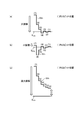
- FIG. 6 is a diagram illustrating the relationship between the voltage of a pixel signal and the voltage of a threshold voltage signal, using a 7-bit A / D converter as an example.
- FIG. 6 is a diagram illustrating the relationship between the voltage of a pixel signal and the voltage of a threshold voltage signal, using a 7-bit A / D converter as an example.
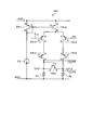
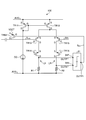
- It is a detailed block diagram of the preamplifier part of 1st Embodiment. It is explanatory drawing of the circuit structural example of a threshold value determination circuit. It is a processing flowchart of a threshold determination circuit (threshold determination path). It is a detailed block diagram of the preamplifier part of the 2nd modification of 1st Embodiment.
- FIG. 1 is a block diagram showing a configuration example of a solid-state image sensor according to the embodiment.
- the solid-state imaging device 1 includes a pixel array unit 2, a row scanning circuit 3, a signal processing unit 4, a timing control unit 5, a column scanning circuit 6, and an image processing unit 7.
- the pixel array unit 2 is provided with a plurality of scanning lines and a plurality of signal lines, and pixel circuits are arranged at the intersections of the respective scanning lines and the respective signal lines to form a two-dimensional array.
- a plurality of pixel circuits are provided in a grid pattern.
- the row scanning circuit 3 sets any one of the plurality of scanning lines in an active state and configures the pixel array unit 2 corresponding to the scanning line in the active state.
- the pixel circuits for one row are driven to output pixel signals.
- the signal processing unit 4 has a plurality of A / D converters, which will be described later, and performs signal processing such as A / D conversion of input pixel signals to generate pixel data.
- the timing control unit 5 controls the timing at which the row scanning circuit 3, the signal processing unit 4, and the column scanning circuit 6 operate.
- the column scanning circuit 6 operates under the control of the timing control unit 5 in synchronization with the operations of the row scanning circuit 3 and the signal processing unit 4, and outputs the signal processed by the signal processing unit 4 for each signal line to pixel data. Are sequentially transferred to the image processing unit 7.
- the image processing unit 7 performs various image processing on image data composed of a plurality of pixel data. In this image processing, for example, demosaicing processing, white balance processing, etc. are executed. Then, the image data after the image processing is transmitted to a recording device such as an external image memory.
- the image processing unit 7 is arranged inside the solid-state image sensor 1, but the image processing unit 7 can be separately provided outside the solid-state image sensor 1.
- each of the circuits in the solid-state imaging device 1 may be arranged on a single semiconductor substrate or may be arranged dispersedly on a plurality of laminated semiconductor substrates.
- FIG. 2 is a diagram illustrating a configuration example of an embodiment of an A / D converter to which the present technology is applied.
- the A / D converter 10 includes a local reference voltage generation unit 11, a DA conversion unit 12, a preamplifier unit 13, a comparator unit 14, a successive conversion logic unit 15, and a rotation logic unit 16.
- a plurality of local reference voltage generation units 11 are provided in the signal processing unit 4, and are used in the A / D converter 10 based on the reference reference signal (reference reference voltage) STref supplied from the reference voltage generation unit 5A.
- a plurality of types of local reference reference signals (local reference reference voltages) Sref are generated and output.
- the DA converter 12 uses a plurality of types of local reference reference signals Sref generated by the local reference voltage generator 11, and controls the digital / analog (D) of the control data D CNT under the control of a sequential conversion logic unit and a rotation logic unit described later. / A) conversion is performed and the threshold voltage signal S th is output.
- the preamplifier unit 13 amplifies the pixel signal S VSL and the threshold voltage signal S th input from the pixel signal input terminal T VSL of the pixel array unit 2, and outputs differential signals OUTP and OUTN.
- the comparator unit 14 compares the differential signals OUTP and OUTN output from the preamplifier unit and outputs a comparison result D CMP .
- the successive conversion logic unit 15 outputs digital control data D SAR (for example, 13 bits) for generating the threshold voltage signal S th from the comparison result data D CMP .
- the pixel data is sequential conversion logic unit 15, and stores the comparison result data D CMP inputted, an analog / digital (A / D) conversion result of a pixel signal S VSL on the basis of the comparison result data D CMP stored D VSL is output from the output terminal TD OUT .
- the rotation logic unit 16 generates and outputs the data DROT based on the pseudo random number data D PN supplied from the pseudo random number generation unit 4B provided in the signal processing unit 5.
- the A / D converter 10 sets the value (“1” or “0”) of all bits by performing successive comparison from the most significant bit to the least significant bit of the pixel data D VSL that is the A / D conversion result. is doing.
- the successive conversion logic unit 15 sets all bits to the center voltage (Vrc) as an initial value.
- the pseudo random number generation unit 4B supplies the rotation logic unit 16 with the pseudo random number data D PN .
- the preamplifier unit 13 amplifies the difference between the input pixel signal S VSL and the threshold voltage signal S th , generates differential signals OUTP and OUTN, and outputs them to the comparator unit 14.
- the comparator unit 14 compares the voltages of the differential signals OUTP and OUTN and outputs the comparison result data D CMP to the successive conversion logic unit 15.
- Sequential conversion logic unit 15 control data D SAR of the DA converter 12 according to the result of the comparison result data D CMP, to store data generation and the comparison result data D CMP of D ROT.
- the DA conversion unit 12 uses the plurality of types of local reference reference signals Sref generated by the local reference voltage generation unit 11 to perform digital / analog (D / A) conversion of the input control data D CNT to generate the threshold voltage signal S.
- the th is output to the preamplifier unit 13.
- the successive conversion logic unit 15 determines and stores the value of each bit. Then, when the values of all the bits are determined, the stored data is output from the output terminal TD OUT as A / D conversion result data.
- FIG. 3 is a diagram illustrating the relationship between the voltage of the pixel signal and the voltage of the threshold voltage signal, using the 7-bit A / D converter as an example.
- the lower side is a state where the voltage is low (white side), and the upper side is a state where the voltage is high (black side).
- the horizontal axis is time.
- the x-th bit at the time of A / D conversion is represented by (x).
- the input signal at the time of MSB conversion corresponds to (7)
- the LSB corresponds to (1).
- FIG. 3A shows a large difference between the voltage of the pixel signal S VSL and the voltage of the threshold voltage signal S th voltage at the start of comparison, but when the difference is within the A / D conversion range, FIG.
- FIG. 3C shows the voltage of the pixel signal S VSL and the threshold voltage signal. This is the case where the voltage difference of S th is extremely large (excessive amplitude) and is outside the range of A / D conversion.
- the successive conversion A / D converter in order to change the threshold voltage S th so as to approach the pixel signal S VSL according to the comparison result of the comparator, when the pixel signal is within the range (FIG. 3A, ( In (b)), at the time of LSB conversion (1), the difference between the pixel signal S VSL and the threshold voltage S th is small and is 1 LSB or less.
- the difference between the pixel signal S VSL and the threshold voltage S th is large even at the time of LSB conversion (1) and is not less than 1 LSB. Since the comparison time of the comparator changes exponentially with respect to the input signal, the comparison time difference due to this input difference appears as streaking.
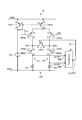
- FIG. 4 is a detailed configuration diagram of the preamplifier unit 13 of the first embodiment.
- the preamplifier unit 13 has a source terminal S connected to a power supply line AVD, a gate terminal G connected to a drain terminal D, and a diode-connected P-channel MOS transistor TR11, and a power supply line AVD connected to a source terminal S and a gate.
- the terminal G is connected to the gate terminal G of the P-channel MOS transistor TR11, and the P-channel MOS transistor TR12 functions as a current mirror circuit in cooperation with the P-channel MOS transistor TR11.
- One end of the P-channel MOS transistor TR11 has a drain terminal D. And a constant current source CC whose other end is connected to the ground line AVS.
- the pixel signal S VSL is input to the gate terminal G
- the source terminal S is connected to the drain terminal D of the P-channel MOS transistor TR12
- the source terminal S is a P-channel MOS transistor.
- the threshold voltage signal S th is input to the gate terminal G
- the source terminal S is connected to the drain terminal D of the P channel MOS transistor TR12
- the source terminal S is the P channel MOS transistor TR15.
- a P-channel MOS transistor TR16 which is connected to the drain terminal D of the MOS transistor TR15 and a bias voltage BIAS is input to the gate terminal G and functions as a cascode circuit, and one end of which is connected to the drain terminal D of the P-channel MOS transistor TR16.
- a second load resistor R2 having an end connected to the ground line AVS.
- one input terminal is connected to the drain terminal of the P-channel MOS transistor TR14 to receive the first output signal OUTP, and the other input terminal is connected to the drain terminal of the P-channel MOS transistor TR16.
- the second output signal OUTN is input, the threshold value determination circuit 21 that outputs the determination result signal S EV by comparing the first output signal OUTP and the second output signal OUTN is provided.
- the drain terminal D is connected to the connection point CP1 of the drain terminal D of the P-channel MOS transistor TR13 and the source terminal of the P-channel MOS transistor TR14, and the drain terminal D of the P-channel MOS transistor TR15 and the P-channel MOS transistor are connected.
- the source terminal D is connected to the connection point CP2 of the source terminal of the transistor TR16, and the determination result signal S EV output from the threshold value determination circuit 21 is input to the gate terminal G to short-circuit the connection points CP1 and CP2.
- an N-channel MOS transistor TR17 functioning as an element (switch).
- the N-channel MOS transistor TR17 constitutes a clamp circuit.
- the P-channel MOS transistor TR13, P-channel MOS transistor TR14, P-channel MOS transistor TR15, P-channel MOS transistor TR16, first load resistor R1 and second load resistor R2 form a differential amplifier DA. .
- the difference between the voltages of the pixel signal S VSL and the threshold voltage signal S th during the LSB conversion is small, and thus the first output signal OUTP output from the preamplifier unit 13 is generated.
- the difference between the second output signal OUTN and the second output signal OUTN is also small.
- the output of the preamplifier unit 13 is also obtained in the LSB conversion. , The difference between the first output signal OUTP and the second output signal OUTN remains large.
- the pixel signal S VSL is determined to be within the A / D conversion range and the N-channel MOS transistor is determined.
- the TR17 remains in the off state (open state). After that, normal A / D conversion processing is executed.
- FIG. 5 is an explanatory diagram of a circuit configuration example of the comparator unit 14.
- the comparator section 14 roughly includes an amplification section (amplification stage) 14A and a latch section 14B.
- the source terminal S is connected to the digital power supply DVD
- the gate terminal G is connected to the clock signal line CLK
- the drain terminal D is connected to the drain terminal of the P-channel MOS transistor TR21.
- An N-channel MOS transistor TR22 whose gate terminal G is connected to the positive side input terminal INP, a P-channel MOS transistor TR23 whose source terminal S is connected to the digital power supply DVD, and whose gate terminal is connected to the clock signal line CLK,
- the drain terminal D is connected to the drain terminal D of the P-channel MOS transistor TR23, the gate terminal G is connected to the negative side input terminal INN, and the drain terminal D is the source of the N-channel MOS transistor TR22.
- a terminal S and a source terminal S of the N-channel MOS transistor TR24 are commonly connected, a gate terminal G is connected to the clock signal line CLK, and a source terminal S is connected to the digital ground DVS.
- the amplifier 14A includes inverters TR31, TR32 and TR33, TR34, which cooperate to amplify the signal.
- the latch unit 14B has a source terminal S connected to the digital power supply DVD, a gate terminal G connected to the clock signal line CLK, a P-channel MOS transistor TR41, a source terminal S connected to the digital power supply DVD, and a drain terminal D.
- the P-channel MOS transistor TR42 connected to the drain terminal D of the P-channel MOS transistor TR41, the drain terminal D connected to the drain terminal D of the P-channel MOS transistor TR41 and the drain terminal D of the P-channel MOS transistor TR42, and the gate terminal G Is an N-channel MOS transistor TR43 connected to the drain terminal D of the P-channel MOS transistor TR31 and the drain terminal D of the N-channel MOS transistor TR32, and the drain terminal D is an N-channel MOS transistor.
- the source terminal S is connected to the digital ground DVS
- the gate terminal G is provided with an N-channel MOS transistor TR44 connected to the gate terminal G of the P-channel MOS transistor TR42, a.
- the latch unit 14B has a source terminal S connected to the digital power supply DVD, a gate terminal G connected to the clock signal line CLK, a P-channel MOS transistor TR45, a source terminal S connected to the digital power supply DVD, and a drain terminal.
- D is connected to the drain terminal D of the P-channel MOS transistor TR45
- the gate terminal G is connected to the drain terminal D of the P-channel MOS transistor TR42 and the drain terminal D of the N-channel MOS transistor TR43.
- the terminal D is connected to the drain terminal D of the P-channel MOS transistor TR45 and the drain terminal D of the P-channel MOS transistor TR46
- the gate terminal G is connected to the drain terminal D of the P-channel MOS transistor TR33.
- the N-channel MOS transistor TR47 connected to the drain D of the N-channel MOS transistor TR34, the drain terminal D is connected to the source terminal S of the N-channel MOS transistor TR47, the source terminal S is connected to the digital ground DVS, and the gate terminal G Of the N-channel MOS transistor TR48 connected to the gate terminal G of the P-channel MOS transistor TR46.
- the comparator unit 14 outputs the comparator output OUTP according to the input signals INP and INN at the rising edge of the clock signal line CLK.
- FIG. 6 is a processing flowchart of the excessive input determination circuit (threshold determination circuit).
- the threshold voltage S th is set to the excessive input determination voltage V th for determining the excessive input (step S11).
- the function of the D / A converter 12 may be expanded, or a separate setting circuit may be provided.
- the threshold value determination circuit 21 is used to compare the pixel signal S VSL with the excessive input determination voltage V th , and whether or not the pixel signal S VSL is lower than the excessive input determination voltage V th (the range of the A / D converter 10 when the input is excessive). It is determined whether or not it is outside (step S12).
- the threshold determination circuit may make the determination using the comparator unit 14.
- the threshold determination circuit 21 is the gate terminal of the P-channel MOS transistor TR13 which is one input terminal of the differential amplifier. It is determined that no excessive input (excessive voltage input) is applied to G, and the "L" level determination result signal S EV is output to the gate terminal G of the N-channel MOS transistor TR17.
- the N-channel MOS transistor TR17 maintains the off state (open state) (step S14).
- the differential amplifier DA maintains the normal operation state.
- step S12 when the pixel signal S VSL is lower than the excessive input determination voltage V th in the determination of step S12 (in the case of excessive input and outside the range of the A / D converter 10) in the determination of step S12, (step S12). Yes), and it is determined that an excessive input (excessive voltage input) is applied to the gate terminal G of the P-channel MOS transistor TR13 that is one input terminal of the differential amplifier DA, and an "H" level determination result signal. S EV is output to the gate terminal G of the N-channel MOS transistor TR17.
- step S13 the N-channel MOS transistor TR17 is turned on (closed) (step S13).
- step S13 the connection point CP1 and the connection point CP2 are short-circuited, and the output voltages OUTP and OUTN become substantially equal.
- the voltage difference input to the comparator unit 14 becomes a very small value.
- the input to the comparator unit 14 can be made small even at the time of excessive input operation, and the conversion speed can be made the same as that of other pixel signals, so that the deterioration of streaking can be suppressed.
- the threshold voltage S th is once set to the excessive input determination voltage V th, and the determination result of the threshold determination circuit 21 is directly output to the gate terminal G of the N-channel MOS transistor TR17.
- a / D conversion is performed as a normal operation, and when the determination result of the comparator unit 14 is “H” continuously from the upper bits, the excessive input is exceeded.
- the operation of the first embodiment is realized only by changing the N-channel MOS transistor TR17, the wiring from the successive conversion logic unit 15 to the gate terminal G, and the control program of the successive conversion logic unit 15. It becomes possible to do.
- FIG. 7 is a detailed configuration diagram of the preamplifier unit of the second modification of the first embodiment. 7, the same parts as those in FIG. 4 are designated by the same reference numerals.
- the difference between the preamplifier unit 13A of the second modification of the first embodiment and the preamplifier unit 13 of the first embodiment is that the voltage of the pixel signal S VSL is compared with a reference comparison voltage V th corresponding to a predetermined excessive input state.
- the drain terminal D is connected to the connection point CP11 of the drain terminal D and the resistor R1 of the P-channel MOS transistor TR14, a drain terminal D and the resistance of the P-channel MOS transistor TR16 Te
- the source terminal S is connected to the connection point CP12 of R2
- the determination result signal S EVA output from the comparison and determination circuit 25 is input to the gate terminal G to function as a switch for short-circuiting the connection points CP11 and CP12.
- the channel MOS transistor TR17A is provided.
- the N-channel MOS transistor TR17A when the voltage of the pixel signal S VSL becomes lower than the reference comparison voltage V th corresponding to the predetermined excessive input state, the N-channel MOS transistor TR17A is turned on. Since it is in the (closed state), the connection point CP11 and the connection point CP12 are short-circuited, the voltages of the preamplifier outputs OUTP and OUTN become substantially equal, and the voltage difference input to the comparator unit 14 can be reduced.
- FIG. 8 is a detailed configuration diagram of the preamplifier section of the third modification example of the first embodiment. 8, the same parts as those in FIG. 4 are designated by the same reference numerals.
- the preamplifier unit 13B of the third modification of the first embodiment is different from the preamplifier unit 13 of the first embodiment in that the voltage of the pixel signal S VSL is compared with a reference comparison voltage V th corresponding to a predetermined excessive input state.
- the comparison determination circuit 25 for outputting the determination result signal S EVB is provided, and the determination result of the comparison determination circuit 25 is input to the gate terminal G of the N-channel MOS transistor TR17B.
- the N-channel MOS transistor TR17B when the voltage of the pixel signal S VSL becomes lower than the reference comparison voltage V th corresponding to the predetermined excessive input state, the N-channel MOS transistor TR17B is turned on. Since it is in the (closed state), the voltages of the preamplifier outputs OUTP and OUTN are substantially equal, and the voltage difference input to the comparator unit 14 can be reduced.
- the configuration of the MOS transistor at the input stage of the preamplifier section 13B is the P-channel MOS transistor configuration, but it is also possible to adopt the N-channel MOS transistor configuration.
- FIG. 9 is a detailed configuration diagram of the preamplifier unit of the second embodiment. 9, the same parts as those in the first embodiment shown in FIG. 4 are designated by the same reference numerals.
- the preamplifier unit 13C of the second embodiment is different from the preamplifier unit 13 of the first embodiment in that it includes an N-channel MOS transistor TR51 functioning as a diode instead of the N-channel MOS transistor TR17 and the threshold value judgment circuit 21. .
- the N-channel MOS transistor TR51 has the drain terminal D connected to the connection point CP11 of the drain terminal D of the P-channel MOS transistor TR14 and the resistor R1 and the connection point of the drain terminal D of the P-channel MOS transistor TR16 and the resistor R2.
- the source terminal S is connected to CP12, and the gate terminal G is connected to the connection point CP11.
- this method does not require a comparison time for excessive input determination or a feedback signal from the successive conversion logic unit 15.
- the gate terminal G of the N-channel MOS transistor TR51 functioning as a diode is also one of the characteristics that are connected to the pixel signal S VSL side.
- FIG. 10 is a detailed configuration diagram of the preamplifier unit of the first modified example of the second embodiment.
- the preamplifier unit 13D of the second embodiment is different from the preamplifier unit 13 of the first embodiment in that the N-channel MOS transistor TR52 functioning as a diode is provided instead of the N-channel MOS transistor TR17 and the threshold value judgment circuit 14. .
- the N-channel MOS transistor TR52 has the drain terminal D connected to the connection point CP1 of the drain terminal D of the P-channel MOS transistor TR13 and the source terminal S of the P-channel MOS transistor TR14, and the drain terminal of the P-channel MOS transistor TR15.
- the source terminal S is connected to the connection point CP2 of the source terminals S of the D and P channel MOS transistors TR16, and the gate terminal G is connected to the connection point CP1.
- the N-channel MOS transistor TR52 is The ON state (conduction state) is established, and the differential voltage between the first output signal OUTP and the second output signal OUTN can be reduced.
- the comparison time for threshold determination and the feedback signal from the successive conversion logic unit 15 are unnecessary.
- the gate terminal G of the N-channel MOS transistor TR52 functioning as a diode is connected to the pixel signal S VSL side. It is also one of the features. However, in order to match the load capacitance, it is also possible to connect an N-channel MOS transistor similar to TR52 to the CP2 side gate and drain, and connect the CP1 side to the source.
- the configuration of the MOS transistor at the input stage of the preamplifier section 13C is the P-channel MOS transistor configuration, but it is also possible to adopt the N-channel MOS transistor configuration.
- FIG. 11 is a detailed configuration diagram of the preamplifier unit according to the third embodiment. 11, the same parts as those in the first embodiment of FIG. 4 are designated by the same reference numerals.
- the preamplifier unit 13E of the third embodiment is different from the preamplifier unit 13 of the first embodiment in that the reference pixel signal conversion is performed based on the determination result signal S EV output by the threshold value determination circuit 21 instead of the N-channel MOS transistor TR17.
- the point is that the P-channel MOS transistor TR53 is applied to the gate terminal G of the P-channel MOS transistor TR13 as the initial voltage VSET corresponding to the time.
- the drain terminal D is connected to the gate terminal G of the P-channel MOS transistor TR13, and the gate terminal G is connected to the output terminal OUTP1 of the threshold value judgment circuit 21.
- the threshold value determination circuit 21 detects that the voltage of the pixel signal S VSL has become lower than the reference comparison voltage V th corresponding to a predetermined excessive input state
- the P-channel MOS Since the transistor TR53 is turned on (closed), the initial voltage VSET is applied to the gate terminal G of the P-channel MOS transistor TR13 of the preamplifier section 13E, and the same conversion as that at the time of converting the reference pixel signal is performed. Therefore, the influence on the other columns is the same as that at the time of converting the reference pixel signal, so that the influence after CDS (Correlated Double Sampling) is small, and the deterioration of the streaking amount can be suppressed.
- CDS Correlated Double Sampling
- FIG. 12 is a detailed configuration diagram of the preamplifier unit of the first modification of the third embodiment. 12, the same parts as those in the third embodiment shown in FIG. 11 are designated by the same reference numerals.
- the preamplifier unit 13F of the first modified example of the third embodiment is different from the preamplifier unit 13E of the third embodiment in that the voltage of the pixel signal S VSL is compared with a reference comparison voltage V th corresponding to a predetermined excessive input state.
- a threshold judgment circuit 30 for outputting the judgment result signal S EVF to the gate terminal G of the P-channel MOS transistor TR53.
- the P-channel MOS transistor TR53 when the voltage of the pixel signal S VSL becomes lower than the reference comparison voltage V th corresponding to the predetermined excessive input state, the P-channel MOS transistor TR53 is turned on. Since it is in the (closed state), the initial voltage VSET is applied to the gate terminal G of the P-channel MOS transistor TR13 of the preamplifier unit 13F, and the same conversion as that at the time of converting the reference pixel signal is performed, so that there is an influence on other columns. Becomes the same as when the reference pixel signal is converted, the influence after CDS (Correlated Double Sampling) becomes small, and the deterioration of the streaking amount can be suppressed.
- CDS Correlated Double Sampling
- FIG. 13 is an explanatory diagram of an example of the initial voltage setting circuit.
- the initial voltage setting circuit guarantees the drain terminal-source terminal voltage Vds of the P-channel MOS transistor TR12 functioning as a current source by the voltage drop of the resistor R3, and at the same time, the gate terminal of the P-channel MOS transistor TR13 of the preamplifier section 13.
- the initial value voltage VSET applied to G is defined and set.
- FIG. 14 is a schematic configuration block diagram of the signal processing unit of the fourth embodiment.
- the signal processing unit 4A shown in FIG. 14 is an example in which one A / D converter processes each of eight pixels in a time-division manner, and for simplification of the drawing, 2n (n: natural number).
- n A / D converters 10-1 to 10-n are shown. In reality, the remaining n A / D converters are arranged above the output signal lines from the pixels extending upward.
- the A / D converters 10-1 to 10-n have the same configuration as the A / D converter 10 shown in FIG. 2, and in FIG. 14, the DA conversion unit 12 and the preamplifier unit are used. 13, the comparator unit 14, the successive conversion logic unit 15, and the rotation logic unit 16 are illustrated.
- each A / D converter 10-1 of the 16 pixels of the pixels PX1 to PX4, the pixels PX11 to PX14, the pixels PX21 to PX24, and the pixels PX31 to PX34 in the case of FIG. Pixels are assigned.
- pixel PX1 eight pixels of a pixel PX1, a pixel PX3, a pixel PX11, a pixel PX13, a pixel PX21, a pixel PX23, a pixel PX31, and a pixel PX33 are allocated to the A / D converter 10-1 shown in the figure. Has been.
- pixels of pixel PX2, pixel PX4, pixel PX12, pixel PX14, pixel PX22, pixel PX24, pixel PX32, and pixel PX3 are assigned.
- the A / D converter 10-1 performs processing in the order of pixel PX1 ⁇ pixel PX3 ⁇ pixel PX11 ⁇ pixel PX13 ⁇ pixel PX21 ⁇ pixel PX23 ⁇ pixel PX31 ⁇ pixel PX33, for example, when data is read once.
- the DA conversion unit 12 of the A / D converter 10-1 uses the plurality of types of local standard reference signals Sref generated by the local reference voltage generation unit 11. , And performs digital / analog (D / A) conversion of the control data D CNT under the control of the later-described successive conversion logic unit and rotation logic unit, and outputs the threshold voltage signal S th to the preamplifier 13.
- the preamplifier unit 13 amplifies the pixel signal S VSL corresponding to the pixel PX1 input from the pixel signal input terminal TSL1 and the threshold voltage signal S th input from the DA converter 12, and outputs the amplified signal to the comparator unit 14. .
- the comparator unit 14 compares the preamplifier outputs and outputs the comparison result data D CMP to the successive conversion logic unit 15.
- the comparison result data D CMP outputs a sequential conversion control data D SAR for performing sequential conversion control for analog / digital conversion, and stores the comparison result data D CMP inputted, stores and outputs the pixel data D VSL is an analog / digital (a / D) conversion result of the pixel signal S VSL from the output terminal TD OUT based on the comparison result data D CMP.
- the A / D converter 10-1 receives the pixel PX3 input from the pixel signal input terminal TSL2 and the pixel signal input terminal TSL3 in the same manner.
- the pixel signal S VSL corresponding to each of the pixels PX33 input from the pixel signal input terminal TSL8 is subjected to analog / digital (A / D) conversion, and output from the output terminal TD OUT .
- the A / D converters 10-2 to 10-n and the n A / D converters simultaneously perform the same processing in parallel.
- the number of A / D converters is about 1 as compared with the case where A / D converters are provided for each pixel. / 8, which makes it possible to reduce the circuit area of the signal processing unit 4A, and hence the installation area of the solid-state image sensor, and to reduce the size of the apparatus.
- FIG. 15 is a block diagram of an example of an indirect light time-of-flight distance sensor to which the present technology is applied.
- An indirect-time of flight type distance sensor 100 includes a sensor chip 101 and a circuit chip 102 stacked on the sensor chip 101.
- the pixel array unit 112 includes a plurality of pixels 111 arranged in an array on the sensor chip 101 in a two-dimensional grid pattern.
- the pixel array unit 112 may be arranged in a matrix and may include a plurality of column signal lines. Each column signal line is connected to each pixel.
- a vertical drive circuit 113, a column signal processing unit 114, a timing adjustment circuit 115, and an output circuit 116 are arranged on the circuit chip 102.
- the vertical drive circuit 113 is configured to drive pixels and output pixel signals to the column signal processing unit 114.
- the column signal processing unit 114 performs A / D conversion processing on the input pixel signal, and outputs the pixel data subjected to A / D conversion processing to the output circuit 116.
- the output circuit 116 performs CDS (Correlated Double Sampling) processing or the like on the pixel data from the column signal processing unit 114, and outputs the pixel data to the signal processing circuit in the subsequent stage.
- CDS Correlated Double Sampling
- the timing control circuit 115 is configured to control the drive timing of each vertical drive circuit 113.
- the column signal processing unit 114 and the output circuit 116 operate in synchronization with the vertical synchronizing signal output from the timing control circuit 115.
- FIG. 16 is a circuit diagram showing a configuration example of a pixel according to the embodiment of the present technology.
- a plurality of pixels 111 are arranged in a two-dimensional grid pattern, and each pixel 111 receives infrared light and is photoelectrically converted into a pixel signal.
- the vertical signal line VSL1 and the vertical signal line VSL2 are arranged in the vertical direction for each column of the pixels 111.
- M is an integer
- a total of 2 ⁇ M vertical signal lines are wired.
- Each pixel has two taps.
- the vertical signal line VSL1 is connected to the tap A of the pixel 111
- the vertical signal line VSL2 is connected to the tap B of the pixel 111.
- the vertical signal line VSL1 transmits the pixel signal AINP1
- the vertical signal line VSL2 transmits the pixel signal AINP2.
- the vertical driving circuit 113 sequentially selects and drives the rows of the pixel area 112, and causes the pixel signals AINP1 and AINP2 to be simultaneously output for each pixel block 221 in the rows. In other words, the vertical drive circuit 113 drives the 2kth row and the 2k + 1th row of the pixel 111 at the same time.
- the pixel 111 includes a photodiode 121, two transfer transistors 122 and 123, two reset transistors 124 and 125, two taps (floating diffusion layers 126 and 127), two amplification transistors 128 and 129, and two selection transistors 130. 131 is provided.
- the photodiode 121 photoelectrically converts the received light to generate an electric charge.
- the photodiode 121 is arranged on the back surface with respect to the front surface with the surface on which the circuit is arranged on the semiconductor substrate as the front surface.
- Such a solid-state image sensor is called a backside illumination type solid-state image sensor. Note that instead of the backside illumination type, a frontside illumination type configuration in which the photodiode 121 is arranged on the front surface can also be used.
- the transfer transistor 122 and the transfer transistor 123 sequentially transfer charges from the photodiode 121 to the TAPA 126 and TAPB 127 in accordance with the transfer signal TRG from the vertical drive circuit 113.
- the TAPA 126 and TAPB 127 accumulate the transferred charges and generate a voltage according to the amount of the accumulated charges.
- the overflow transistor 132 is a transistor that sequentially discharges the charges of the photodiode 121 to the high-potential side power supply VDD, and has a function of resetting the photodiode 121.
- the reset transistors 124 and 125 are for extracting charges from the respective TAPA 126 and TAPB 127 in accordance with the reset signal RSTp from the vertical drive circuit 113 to initialize the charge amount.
- the amplification transistors 128 and 129 amplify the voltages of the TAPA 126 and TAPB 127, respectively.
- the selection transistors 130 and 131 output the signal of the amplified voltage as a pixel signal to the column signal processing unit 114 via two vertical signal lines (for example, VSL1 and VSL2). To do.
- the vertical signal line and the vertical signal line VSL2 are connected to the input of one A / D converter 10 in the column signal processing unit 114.
- the circuit configuration of the pixel 111 is not limited to the configuration illustrated in FIG. 15 as long as the pixel signal can be generated by photoelectric conversion.
- the fifth embodiment as in the fourth embodiment, it is possible to reduce the installation area of the solid-state image sensor and to downsize the indirect light time-of-flight distance sensor.
- a comparator circuit that compares threshold voltages to determine whether an excessive input of pixel signals has been input; A result of the comparison is input to a control terminal, and a first transistor forming a clamp circuit; A / D converter provided with.
- the clamp circuit includes a threshold value determination circuit that determines whether or not a signal having a value equal to or greater than a predetermined excessive input threshold value is input as the pixel signal, On the basis of the output of the threshold value judgment circuit, the first transistor short-circuits the first predetermined position and the second predetermined position which are connected during clamping.
- the A / D converter according to any one of (1) to (3).
- a pair of differential pair transistors forming an input current line and a reference current line, A pair of bias transistors for controlling a bias current flowing through the differential pair transistors, A diode having an anode connected to the first predetermined position and a cathode connected to the second predetermined position with respect to a first predetermined position and a second predetermined position to be connected at the time of clamping, A / D converter.
- a pixel array section in which a plurality of pixels for photoelectric conversion are arranged in an array;
- a signal processing unit that reads an analog pixel signal from the pixel array unit and performs signal processing,
- the signal processing unit includes an A / D converter that performs analog / digital conversion of the analog pixel signal,
- the A / D converter includes a comparator circuit that compares a pixel signal and a threshold voltage for determining whether an excessive input is input, A result of the comparison is input as a control terminal, a first transistor forming a clamp circuit, Electronic equipment equipped with.
- a pixel array section in which a plurality of pixels for photoelectric conversion are arranged in an array;
- a signal processing unit that reads an analog pixel signal from the pixel array unit and performs signal processing,
- the signal processing unit includes an A / D converter that performs analog / digital conversion of the analog pixel signal,
- the A / D converter includes a pair of differential pair transistors forming an input current line and a reference current line, A pair of bias transistors for controlling a bias current flowing through the differential pair transistors, A diode having an anode connected to the first predetermined position and a cathode connected to the second predetermined position with respect to a first predetermined position and a second predetermined position to be connected at the time of clamping;
- Electronic equipment equipped with
Landscapes
- Engineering & Computer Science (AREA)
- Multimedia (AREA)
- Signal Processing (AREA)
- Theoretical Computer Science (AREA)
- Analogue/Digital Conversion (AREA)
- Transforming Light Signals Into Electric Signals (AREA)
Abstract
本開示のA/D変換器(10)は、画素信号(SVSL)の過大入力が入力されたかどうか判断する閾値電圧(Vth)の比較を行う比較器回路(21)と、その比較結果が制御端子に入力され、クランプ回路を構成する第1のトランジスタ(TR17)と、を備え、クランプ回路(TR17)をオン状態(閉状態)とすることで第1のトランジスタ(TR17)によりクランプ時に接続される第1の所定位置(CP1)と第2の所定位置(CP2)に流れる電流を等しくする、もしくは第1の所定位置(CP1)と第2の所定位置(CP2)の電圧を等しくするので、画素信号ライン側(TR13、TR14,R1)に過大入力が印加された場合にストリーキングを抑制することができる。
Description
本開示は、A/D変換器及び電子機器に関する。
近年、半導体微細加工技術を応用したCMOS(Complementary Metal Oxide Semiconductor)イメージセンサ等の撮像素子がディジタルカメラやスマートフォン等において広く採用されている。
これらの撮像素子においては、各画素内に設けられた光電変換素子としてのフォトダイオードにおいて、被写体から入射した光が光電変換され、得られた電荷の量に対応する電圧信号が増幅トランジスタ及び垂直信号線を介して読み出されてコンパレータを有するA/D変換器によりアナログ/ディジタル(A/D)変換されて撮像データとして出力される。
CMOS等の撮像素子を用いた撮像装置では、高輝度な被写体を撮像した場合、A/D変換部の一斉反転による電源ノイズの影響によって、撮像画像上で左右方向に延びる帯状のラインノイズ、いわゆるストリーキングが発生することがあり、これを抑制するための技術が提案されている(例えば、特許文献1参照)。
ところで、CMOS等の撮像素子を用いた撮像装置において、逐次変換型のA/D変換器を用いて、高輝度な被写体を撮像した場合、すなわち、画素信号ライン側に過大入力が印加されている場合には、A/D変換部を構成しているプリアンプ部の差動対トランジスタのそれぞれに流れる電流が大きく異なる。
このため、下位ビットの変換時においても差動対トランジスタに流れる電流は大きく異なった状態となっており、コンパレータの比較時間は入力信号に対して指数関数で変わるために、この入力差分による比較時間差がストリーキングとなって表れる虞があった。
本開示は、このような状況に鑑みてなされたものであり、画素信号ライン側に過大入力が印加された場合にストリーキングを抑制することができるA/D変換器及び電子機器を提供することを目的としている。
上記目的を達成するために、本開示のA/D変換器は、画素信号の過大入力が入力されたかどうか判断する閾値電圧の比較を行う比較器回路と、その比較結果が制御端子に入力され、クランプ回路を構成する第1のトランジスタと、を備える。
クランプ回路をオン状態(閉状態)とすることで第1のトランジスタによりクランプ時に接続される第1の所定位置と第2の所定位置に流れる電流を等しくする、もしくは第1の所定位置と第2の所定位置の電圧を等しくする、ことでストリーキングを抑制することができる。
本開示によれば、差動アンプ出力に発生する電圧差を抑制してストリーキングを抑制することができる。なお、ここに記載された効果は必ずしも限定されるものではなく、本開示中に記載されたいずれかの効果であってもよい。
以下に、本開示の実施形態について図面に基づいて詳細に説明する。なお、以下の各実施形態において、同一の部位には同一の符号を付することにより重複する説明を省略する。
(1)第1実施形態
[固体撮像素子の構成例]
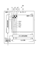
図1は、実施形態における固体撮像素子の一構成例を示すブロック図である。
固体撮像素子1は、画素アレイ部2、行走査回路3、信号処理部4、タイミング制御部5、列走査回路6及び画像処理部7を備えている。
[固体撮像素子の構成例]
図1は、実施形態における固体撮像素子の一構成例を示すブロック図である。
固体撮像素子1は、画素アレイ部2、行走査回路3、信号処理部4、タイミング制御部5、列走査回路6及び画像処理部7を備えている。
上記構成において、画素アレイ部2は、複数の走査線と、複数の信号線とが設けられており、各走査線と各信号線の交差部には、それぞれ画素回路が配置されて、二次元格子状に複数の画素回路が設けられている。
行走査回路3は、タイミング制御部5の制御下で、複数の走査線のうちいずれかの走査線をアクティブ状態とし、当該アクティブ状態とした走査線に対応する画素アレイ部2を構成している一行分の画素回路を駆動して画素信号を出力させるものである。
信号処理部4は、複数の後述するA/D変換器を有し、入力された画素信号のA/D変換等の信号処理を行って画素データを生成する。
タイミング制御部5は、行走査回路3、信号処理部4および列走査回路6のそれぞれが動作するタイミングを制御する。
タイミング制御部5は、行走査回路3、信号処理部4および列走査回路6のそれぞれが動作するタイミングを制御する。
列走査回路6は、タイミング制御部5の制御下で、行走査回路3及び信号処理部4の動作に同期して動作し、信号処理部4において信号線ごとに信号処理された信号を画素データとして順次画像処理部7に転送する。
画像処理部7は、複数の画素データから構成される画像データに対し、様々な画像処理を実行する。
この画像処理においては、例えば、デモザイク処理やホワイトバランス処理などが実行される。
そして、画像処理後の画像データは、外部の画像メモリ等の記録装置に送信される。
この画像処理においては、例えば、デモザイク処理やホワイトバランス処理などが実行される。
そして、画像処理後の画像データは、外部の画像メモリ等の記録装置に送信される。
以上の説明においては、画像処理部7を固体撮像素子1内に配置していたが、この画像処理部7を固体撮像素子1の外部に別体に設けることも可能である。
また、固体撮像素子1内の回路のそれぞれは、単一の半導体基板に配置してもよいし、積層した複数の半導体基板に分散して配置してもよい。
[A/D変換器の構成例]
図2は、本技術を適用したA/D変換器の一実施形態の構成例を説明する図である。
A/D変換器10は、図2に示すように、ローカル参照電圧生成部11、DA変換部12、プリアンプ部13、コンパレータ部14、逐次変換ロジック部15及びローテーションロジック部16を備えている。
図2は、本技術を適用したA/D変換器の一実施形態の構成例を説明する図である。
A/D変換器10は、図2に示すように、ローカル参照電圧生成部11、DA変換部12、プリアンプ部13、コンパレータ部14、逐次変換ロジック部15及びローテーションロジック部16を備えている。
ローカル参照電圧生成部11は、信号処理部4に複数設けられており、参照電圧生成部5Aから供給された基準参照信号(基準参照電圧)STrefに基づいて、当該A/D変換器10において用いる複数種類のローカル基準参照信号(ローカル基準参照電圧)Srefを生成し、出力する。
DA変換部12は、ローカル参照電圧生成部11が生成した複数種類のローカル基準参照信号Srefを用い、後述の逐次変換ロジック部及びローテーションロジック部の制御下で制御データDCNTのディジタル/アナログ(D/A)変換を行って閾値電圧信号Sthを出力する。
プリアンプ部13は、画素アレイ部2の画素信号入力端子TVSLから入力された画素信号SVSL及び閾値電圧信号Sthを増幅し、差動信号OUTP、OUTNを出力する。
コンパレータ部14は、プリアンプ部から出力された差動信号OUTP、OUTNを比較し、比較結果DCMPを出力する。
逐次変換ロジック部15は、比較結果データDCMPから閾値電圧信号Sth生成用のディジタル制御データDSAR(例えば、13ビット)を出力する。また、逐次変換ロジック部15は、入力された比較結果データDCMPを記憶し、記憶した比較結果データDCMPに基づいて画素信号SVSLのアナログ/ディジタル(A/D)変換結果である画素データDVSLを出力端子TDOUTから出力する。
ローテーションロジック部16は、信号処理部5に設けられた疑似乱数生成部4Bから供給された疑似乱数データDPNに基づいてデータDROTを生成して出力する。
[A/D変換器の概要動作]
ここで、A/D変換器10の概要動作について説明する。
ここで、A/D変換器10の概要動作について説明する。
A/D変換器10は、A/D変換結果となる画素データDVSLの最上位ビットから最下位ビットまで逐次比較を行うことにより、全ビットの値(“1”又は“0”)を設定している。
まず、逐次変換ロジック部15は、初期値としてすべてのビットをセンター電圧(Vrc)に設定する。
これと並行して疑似乱数生成部4Bはローテーションロジック部16に、疑似乱数データDPNを供給する。
プリアンプ部13は、入力された画素信号SVSL及び閾値電圧信号Sthの差分を増幅し、差動信号OUTP、OUTNを生成し、コンパレータ部14に出力する。
コンパレータ部14は、差動信号OUTP、OUTNの電圧を比較し、比較結果データDCMPとして逐次変換ロジック部15に出力する。
コンパレータ部14は、差動信号OUTP、OUTNの電圧を比較し、比較結果データDCMPとして逐次変換ロジック部15に出力する。
逐次変換ロジック部15は、比較結果データDCMPの結果に応じてDA変換部12の制御データDSAR、DROTの生成および比較結果データDCMPのデータを記憶する。
DA変換部12は、ローカル参照電圧生成部11が生成した複数種類のローカル基準参照信号Srefを用い、入力された制御データDCNTのディジタル/アナログ(D/A)変換を行って閾値電圧信号Sthをプリアンプ部13に出力する。
以下、同様にして最上位ビット(MSB)~最下位ビット(LSB)まで逐次比較を行い、逐次変換ロジック部15は、各ビットの値を確定し記憶することとなる。
そして、全てのビットの値が確定すると、記憶したデータをA/D変換結果データとして出力端子TDOUTから出力することとなる。
そして、全てのビットの値が確定すると、記憶したデータをA/D変換結果データとして出力端子TDOUTから出力することとなる。
[従来のA/D変換器の問題点]
ここで、A/D変換器における従来技術の問題点について説明する。
図3は、7ビットA/D変換器を例とした、画素信号の電圧と閾値電圧信号の電圧との関係説明図である。
ここで、A/D変換器における従来技術の問題点について説明する。
図3は、7ビットA/D変換器を例とした、画素信号の電圧と閾値電圧信号の電圧との関係説明図である。
図3の画素信号SVSLにおいては、下側が電圧が低い状態(白色側)であり、上側が電圧が高い状態(黒色側)である。横軸は、時間である。
図3において、A/D変換時の第xビットは(x)と表示するものとする。例えば、MSB変換時の入力信号は(7)に対応し、LSBは(1)に対応している。
図3において、A/D変換時の第xビットは(x)と表示するものとする。例えば、MSB変換時の入力信号は(7)に対応し、LSBは(1)に対応している。
図3(a)は、比較開始時点において画素信号SVSLの電圧と閾値電圧信号Sth電圧の電圧との差が大きいがA/D変換のレンジ内の場合、図3(b)は、比較開始時点において、画素信号SVSLの電圧と閾値電圧信号Sthの電圧との差が小さくA/D変換のレンジ内の場合、図3(c)は、画素信号SVSLの電圧と閾値電圧信号Sthの電圧差が非常に大きく(過大振幅)A/D変換のレンジ外の場合である。
逐次変換型のA/D変換器ではコンパレータの比較結果に応じて閾値電圧Sthを画素信号SVSLに近づける様に変更するために、画素信号がレンジ内の場合(図3(a)、(b))には、LSB変換時(1)には画素信号SVSLと閾値電圧Sthの差が小さく1LSB以下となる。
これらに対し、図3(c)に示す例の場合には、LSB変換時(1)においても画素信号SVSLと閾値電圧Sthの差が大きく1LSB以下となっていない。コンパレータの比較時間は入力信号に対して指数関数で変わるために、この入力差分による比較時間差がストリーキングとなって表れる。
[第1実施形態のコンパレータ部の詳細構成]
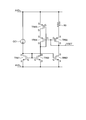
図4は、第1実施形態のプリアンプ部13の詳細構成図である。
プリアンプ部13は、電源ラインAVDにソース端子Sが接続され、ゲート端子Gがドレイン端子Dに接続されダイオード接続とされたPチャネルMOSトランジスタTR11と、電源ラインAVDにソース端子Sが接続され、ゲート端子GがPチャネルMOSトランジスタTR11のゲート端子Gに接続され、PチャネルMOSトランジスタTR11と共働してカレントミラー回路として機能するPチャネルMOSトランジスタTR12と、一端がPチャネルMOSトランジスタTR11のドレイン端子Dに接続され、他端がグランドラインAVSに接続された定電流源CCと、を備えている。
図4は、第1実施形態のプリアンプ部13の詳細構成図である。
プリアンプ部13は、電源ラインAVDにソース端子Sが接続され、ゲート端子Gがドレイン端子Dに接続されダイオード接続とされたPチャネルMOSトランジスタTR11と、電源ラインAVDにソース端子Sが接続され、ゲート端子GがPチャネルMOSトランジスタTR11のゲート端子Gに接続され、PチャネルMOSトランジスタTR11と共働してカレントミラー回路として機能するPチャネルMOSトランジスタTR12と、一端がPチャネルMOSトランジスタTR11のドレイン端子Dに接続され、他端がグランドラインAVSに接続された定電流源CCと、を備えている。
また、プリアンプ部13は、ゲート端子Gに画素信号SVSLが入力され、ソース端子SがPチャネルMOSトランジスタTR12のドレイン端子Dに接続されたPチャネルMOSトランジスタTR13と、ソース端子SがPチャネルMOSトランジスタTR13のドレイン端子Dに接続され、ゲート端子Gにバイアス電圧BIASが入力されて、カスコード回路として機能するPチャネルMOSトランジスタTR14と、一端がPチャネルMOSトランジスタTR14のドレイン端子Dに接続され他端がグランドラインAVSに接続された第一の負荷抵抗R1と、を備えている。
さらに、プリアンプ部13は、ゲート端子Gに閾値電圧信号Sthが入力され、ソース端子SがPチャネルMOSトランジスタTR12のドレイン端子Dに接続されたPチャネルMOSトランジスタTR15と、ソース端子SがPチャネルMOSトランジスタTR15のドレイン端子Dに接続され、ゲート端子Gにバイアス電圧BIASが入力されて、カスコード回路として機能するPチャネルMOSトランジスタTR16と、一端がPチャネルMOSトランジスタTR16のドレイン端子Dに接続され他端がグランドラインAVSに接続された第二の負荷抵抗R2と、を備えている。
さらにまた、プリアンプ部13は、一方の入力端子がPチャネルMOSトランジスタTR14のドレイン端子に接続されて第1出力信号OUTPが入力され、他方の入力端子がPチャネルMOSトランジスタTR16のドレイン端子に接続されて第2出力信号OUTNが入力され、第1出力信号OUTP及び第2出力信号OUTNを比較して判別結果信号SEVを出力する閾値判定回路21と、を備えている。
また、プリアンプ部13は、PチャネルMOSトランジスタTR13のドレイン端子D及びPチャネルMOSトランジスタTR14のソース端子の接続点CP1にドレイン端子Dが接続され、PチャネルMOSトランジスタTR15のドレイン端子D及びPチャネルMOSトランジスタTR16のソース端子の接続点CP2にソース端子Dが接続され、ゲート端子Gに閾値判定回路21が出力した判別結果信号SEVが入力されて接続点CP1及び接続点CP2を短絡するためのスイッチング素子(スイッチ)として機能するNチャネルMOSトランジスタTR17と、を備えている。
上記構成において、NチャネルMOSトランジスタTR17は、クランプ回路を構成している。
また、PチャネルMOSトランジスタTR13、PチャネルMOSトランジスタTR14、PチャネルMOSトランジスタTR15、PチャネルMOSトランジスタTR16、第一の負荷抵抗R1及び第二の負荷抵抗R2は、差動アンプDAを構成している。
また、PチャネルMOSトランジスタTR13、PチャネルMOSトランジスタTR14、PチャネルMOSトランジスタTR15、PチャネルMOSトランジスタTR16、第一の負荷抵抗R1及び第二の負荷抵抗R2は、差動アンプDAを構成している。
画素信号SVSLが所定のA/D変換レンジ内の場合は、LSB変換時に画素信号SVSLと閾値電圧信号Sthの電圧の差分は小さいため、プリアンプ部13の出力である第1出力信号OUTP及び第2出力信号OUTNの差分も小さくなっている。
一方、画素信号SVSLが所定のA/D変換レンジを超える過大入力信号の場合で、NチャネルMOSトランジスタTR17をオフ状態(開状態)とした場合には、LSB変換においてもプリアンプ部13の出力である第1出力信号OUTP及び第2出力信号OUTNの差分は大きいままである。
この場合にNチャネルMOSトランジスタTR17をオン状態(閉状態)とすることで、負荷抵抗R1、R2に流れる電流を等しくでき、第1出力信号OUTP及び第2出力信号OUTNは同電位となる。
したがって、後段に接続するコンパレータ部14の変換時間を同じにすることが出来、コンパレータの変換スピード差によるストリーキング劣化を低減する事が可能となる。
したがって、後段に接続するコンパレータ部14の変換時間を同じにすることが出来、コンパレータの変換スピード差によるストリーキング劣化を低減する事が可能となる。
ここで、過大入力信号の判定方法について記載する。
通常のA/D変換処理前に閾値電圧Sthを過大入力判定電圧Vthに設定し、その過大入力判定電圧Vthと画素信号SVSLの電圧との比較を閾値判定回路21を用いて行う。この結果、画素信号SVSLの電圧の方が低い(閾値電圧としての過大入力判定電圧Vthが高い)場合は、画素信号SVSLは、A/D変換のレンジ外(過大入力信号)であると判定され、NチャネルMOSトランジスタTR17をオン状態(閉状態)とする。
通常のA/D変換処理前に閾値電圧Sthを過大入力判定電圧Vthに設定し、その過大入力判定電圧Vthと画素信号SVSLの電圧との比較を閾値判定回路21を用いて行う。この結果、画素信号SVSLの電圧の方が低い(閾値電圧としての過大入力判定電圧Vthが高い)場合は、画素信号SVSLは、A/D変換のレンジ外(過大入力信号)であると判定され、NチャネルMOSトランジスタTR17をオン状態(閉状態)とする。
一方、画素信号SVSLの電圧の方が高い(閾値電圧としての過大入力判定電圧Vthが低い)場合は、画素信号SVSLは、A/D変換のレンジ内と判定され、NチャネルMOSトランジスタTR17をオフ状態(開状態)のままとする。
その後、通常のA/D変換処理が実行される。
その後、通常のA/D変換処理が実行される。
[コンパレータ部の回路構成例]
ここで、コンパレータ部14の回路構成例について説明する。
図5は、コンパレータ部14の回路構成例の説明図である。
コンパレータ部14は、図5に示すように、大別すると、増幅部(増幅段)14A、ラッチ部14Bを備えている。
増幅部14Aは、ソース端子Sがディジタル電源DVDに接続され、ゲート端子Gがクロック信号ラインCLKに接続されたPチャネルMOSトランジスタTR21と、ドレイン端子DがPチャネルMOSトランジスタTR21のドレイン端子に接続され、ゲート端子Gが正側入力端子INPに接続されたNチャネルMOSトランジスタTR22と、ソース端子Sがディジタル電源DVDに接続され、ゲート端子がクロック信号ラインCLKに接続されたPチャネルMOSトランジスタTR23と、ドレイン端子DがPチャネルMOSトランジスタTR23のドレイン端子Dに接続され、ゲート端子Gが負側入力端子INNに接続されたNチャネルMOSトランジスタTR24とドレイン端子DがNチャネルMOSトランジスタTR22のソース端子S及びNチャネルMOSトランジスタTR24のソース端子Sに共通接続され、ゲート端子Gがクロック信号ラインCLKに接続され、ソース端子SがディジタルグランドDVSに接続されたNチャネルMOSトランジスタTR25と、を備えている。
また、増幅部14AはインバータTR31、TR32およびTR33、TR34を備えており、これらが共働することにより、信号の増幅を行っている。
ここで、コンパレータ部14の回路構成例について説明する。
図5は、コンパレータ部14の回路構成例の説明図である。
コンパレータ部14は、図5に示すように、大別すると、増幅部(増幅段)14A、ラッチ部14Bを備えている。
増幅部14Aは、ソース端子Sがディジタル電源DVDに接続され、ゲート端子Gがクロック信号ラインCLKに接続されたPチャネルMOSトランジスタTR21と、ドレイン端子DがPチャネルMOSトランジスタTR21のドレイン端子に接続され、ゲート端子Gが正側入力端子INPに接続されたNチャネルMOSトランジスタTR22と、ソース端子Sがディジタル電源DVDに接続され、ゲート端子がクロック信号ラインCLKに接続されたPチャネルMOSトランジスタTR23と、ドレイン端子DがPチャネルMOSトランジスタTR23のドレイン端子Dに接続され、ゲート端子Gが負側入力端子INNに接続されたNチャネルMOSトランジスタTR24とドレイン端子DがNチャネルMOSトランジスタTR22のソース端子S及びNチャネルMOSトランジスタTR24のソース端子Sに共通接続され、ゲート端子Gがクロック信号ラインCLKに接続され、ソース端子SがディジタルグランドDVSに接続されたNチャネルMOSトランジスタTR25と、を備えている。
また、増幅部14AはインバータTR31、TR32およびTR33、TR34を備えており、これらが共働することにより、信号の増幅を行っている。
ラッチ部14Bは、ソース端子Sがディジタル電源DVDに接続され、ゲート端子Gがクロック信号ラインCLKに接続されたPチャネルMOSトランジスタTR41と、ソース端子Sがディジタル電源DVDに接続され、ドレイン端子DがPチャネルMOSトランジスタTR41のドレイン端子Dに接続されたPチャネルMOSトランジスタTR42と、ドレイン端子DがPチャネルMOSトランジスタTR41のドレイン端子D及びPチャネルMOSトランジスタTR42のドレイン端子Dに接続され、ゲート端子GがPチャネルMOSトランジスタTR31のドレイン端子D及びNチャネルMOSトランジスタTR32のドレイン端子Dに接続されたNチャネルMOSトランジスタTR43と、ドレイン端子DがNチャネルMOSトランジスタTR43のソース端子Sに接続され、ソース端子SがディジタルグランドDVSに接続され、ゲート端子GがPチャネルMOSトランジスタTR42のゲート端子Gに接続されたNチャネルMOSトランジスタTR44と、を備えている。
また、ラッチ部14Bは、ソース端子Sがディジタル電源DVDに接続され、ゲート端子Gがクロック信号ラインCLKに接続されたPチャネルMOSトランジスタTR45と、ソース端子Sがディジタル電源DVDに接続され、ドレイン端子DがPチャネルMOSトランジスタTR45のドレイン端子Dに接続され、ゲート端子GがPチャネルMOSトランジスタTR42のドレイン端子D及びNチャネルMOSトランジスタTR43のドレイン端子Dに接続されたPチャネルMOSトランジスタTR46と、ドレイン端子DがPチャネルMOSトランジスタTR45のドレイン端子D及びPチャネルMOSトランジスタTR46のドレイン端子Dに接続され、ゲート端子GがPチャネルMOSトランジスタTR33のドレイン端子D及びNチャネルMOSトランジスタTR34のドレインDに接続されたNチャネルMOSトランジスタTR47と、ドレイン端子DがNチャネルMOSトランジスタTR47のソース端子Sに接続され、ソース端子SがディジタルグランドDVSに接続され、ゲート端子GがPチャネルMOSトランジスタTR46のゲート端子Gに接続されたNチャネルMOSトランジスタTR48と、を備えている。
上記構成において、コンパレータ部14は、クロック信号ラインCLKの立ち上がり時の入力信号INP,INNに応じて、コンパレータ出力OUTPを出力する。
[閾値判定回路の動作]
図6は、過大入力判定回路(閾値判定用回路)の処理フローチャートである。
まず、閾値電圧Sthを過大入力と判定する過大入力判定電圧Vthに設定する(ステップS11)。
ここで、電圧の設定の方法は、D/A変換部12の機能を拡張してもよいし、別途設定回路を設けるようにしてもよい。
図6は、過大入力判定回路(閾値判定用回路)の処理フローチャートである。
まず、閾値電圧Sthを過大入力と判定する過大入力判定電圧Vthに設定する(ステップS11)。
ここで、電圧の設定の方法は、D/A変換部12の機能を拡張してもよいし、別途設定回路を設けるようにしてもよい。
続いて、閾値判定回路21を用いて、画素信号SVSLと過大入力判定電圧Vthの比較を行い、過大入力判定電圧Vthより低いか否か(過大入力でA/D変換器10のレンジ外かどうか)を判定する(ステップS12)。閾値判定回路はコンパレータ部14を用いて判定を行ってもよい。
閾値判定回路21は、ステップS12の判定において、画素信号SVSLが過大入力判定電圧より高い場合は(ステップS12;No)、差動アンプの一方の入力端子であるPチャネルMOSトランジスタTR13のゲート端子Gに過大入力(過大電圧入力)は印加されていないと判定して、“L”レベルの判別結果信号SEVをNチャネルMOSトランジスタTR17のゲート端子Gに出力する。
この結果、NチャネルMOSトランジスタTR17は、オフ状態(開状態)を維持する(ステップS14)。
この結果、差動アンプDAは、通常の動作状態を維持することとなる。
この結果、差動アンプDAは、通常の動作状態を維持することとなる。
これに対し、閾値判定回路21は、ステップS12の判定において、画素信号SVSLが過大入力判定電圧Vthより低い場合(過大入力でA/D変換器10のレンジ外の場合)は(ステップS12;Yes)、差動アンプDAの一方の入力端子であるPチャネルMOSトランジスタTR13のゲート端子Gに過大入力(過大電圧入力)が印加されていると判定して、“H”レベルの判別結果信号SEVをNチャネルMOSトランジスタTR17のゲート端子Gに出力する。
この結果、NチャネルMOSトランジスタTR17をオン状態(閉状態)とする(ステップS13)。
この結果、接続点CP1及び接続点CP2が短絡され、出力電圧OUTP,OUTNは、ほぼ等しくなる。
この結果、接続点CP1及び接続点CP2が短絡され、出力電圧OUTP,OUTNは、ほぼ等しくなる。
これにより、過大入力電圧印加時においても、コンパレータ部14に入力される電圧差分は非常に小さな値となる。これにより過大入力動作時においてもコンパレータ部14への入力を小さくすることが出来、変換スピードを他の画素信号と同様にすることが出来るため、ストリーキングの劣化を抑制することが可能となる。
[第1実施形態の効果]
以上の説明のように、本第1実施形態によれば、差動アンプDAに過大入力が印加された場合でも、下位ビット変換時の応答時間を差動アンプDAに過大入力が印加されていない場合と同様とすることができ、ストリーキングの劣化を抑制することが可能となる。
以上の説明のように、本第1実施形態によれば、差動アンプDAに過大入力が印加された場合でも、下位ビット変換時の応答時間を差動アンプDAに過大入力が印加されていない場合と同様とすることができ、ストリーキングの劣化を抑制することが可能となる。
[第1実施形態の第1変形例]
以上の説明においては、一度閾値電圧Sthを過大入力判定電圧Vthに設定し閾値判定回路21の判定結果を直接NチャネルMOSトランジスタTR17のゲート端子Gに出力する構成を採っていた。
しかしながら、一度過大入力判定電圧Vthに設定するのではなく、通常動作としてA/D変換を行っていき、上位から数Bit続けてコンパレータ部14の判定結果が“H”の場合に、過大入力と判定し、NMOSトランジスタTR17をオン状態にするといった構成にすることも可能である。この場合は過大入力判定電圧Vthへの設定および過大入力判定を行う必要が無いので、実際のA/D変換以外に余計なA/D変換時間が不要となり、処理の高速化が図れる。
以上の説明においては、一度閾値電圧Sthを過大入力判定電圧Vthに設定し閾値判定回路21の判定結果を直接NチャネルMOSトランジスタTR17のゲート端子Gに出力する構成を採っていた。
しかしながら、一度過大入力判定電圧Vthに設定するのではなく、通常動作としてA/D変換を行っていき、上位から数Bit続けてコンパレータ部14の判定結果が“H”の場合に、過大入力と判定し、NMOSトランジスタTR17をオン状態にするといった構成にすることも可能である。この場合は過大入力判定電圧Vthへの設定および過大入力判定を行う必要が無いので、実際のA/D変換以外に余計なA/D変換時間が不要となり、処理の高速化が図れる。
このような構成を採ることにより、NチャネルMOSトランジスタTR17、逐次変換ロジック部15からゲート端子Gへの配線及び逐次変換ロジック部15の制御プログラムを変更するだけで、第1実施形態の動作を実現することが可能となる。
[第1実施形態の第2変形例]
図7は、第1実施形態の第2変形例のプリアンプ部の詳細構成図である。
図7において、図4と同様の部分には、同一の符号を付すものとする。
第1実施形態の第2変形例のプリアンプ部13Aが第1実施形態のプリアンプ部13と異なる点は、画素信号SVSLの電圧を所定の過大入力状態に相当する基準比較電圧Vthと比較して判別結果信号SEVAを出力する比較判定回路25と、PチャネルMOSトランジスタTR14のドレイン端子D及び抵抗R1の接続点CP11にドレイン端子Dが接続され、PチャネルMOSトランジスタTR16のドレイン端子D及び抵抗R2の接続点CP12にソース端子Sが接続され、ゲート端子Gに比較判定回路25が出力した判別結果信号SEVAが入力されて接続点CP11及び接続点CP12を短絡するためのスイッチとして機能するNチャネルMOSトランジスタTR17Aと、を備えた点である。
図7は、第1実施形態の第2変形例のプリアンプ部の詳細構成図である。
図7において、図4と同様の部分には、同一の符号を付すものとする。
第1実施形態の第2変形例のプリアンプ部13Aが第1実施形態のプリアンプ部13と異なる点は、画素信号SVSLの電圧を所定の過大入力状態に相当する基準比較電圧Vthと比較して判別結果信号SEVAを出力する比較判定回路25と、PチャネルMOSトランジスタTR14のドレイン端子D及び抵抗R1の接続点CP11にドレイン端子Dが接続され、PチャネルMOSトランジスタTR16のドレイン端子D及び抵抗R2の接続点CP12にソース端子Sが接続され、ゲート端子Gに比較判定回路25が出力した判別結果信号SEVAが入力されて接続点CP11及び接続点CP12を短絡するためのスイッチとして機能するNチャネルMOSトランジスタTR17Aと、を備えた点である。
本第1実施形態の第2変形例によっても、画素信号SVSLの電圧が所定の過大入力状態に相当する基準比較電圧Vthよりも低くなった場合には、NチャネルMOSトランジスタTR17Aをオン状態(閉状態)とするので、接続点CP11及び接続点CP12が短絡され、プリアンプ出力OUTP、OUTNの電圧はほぼ等しくなり、コンパレータ部14に入力される電圧差を小さくすることが可能となる。
[第1実施形態の第3変形例]
図8は、第1実施形態の第3変形例のプリアンプ部の詳細構成図である。
図8において、図4と同様の部分には、同一の符号を付すものとする。
第1実施形態の第3変形例のプリアンプ部13Bが第1実施形態のプリアンプ部13と異なる点は、画素信号SVSLの電圧を所定の過大入力状態に相当する基準比較電圧Vthと比較して判別結果信号SEVBを出力する比較判定回路25、を備え、比較判定回路25の判定結果をNチャネルMOSトランジスタTR17Bのゲート端子Gに入力するようにした点である。
図8は、第1実施形態の第3変形例のプリアンプ部の詳細構成図である。
図8において、図4と同様の部分には、同一の符号を付すものとする。
第1実施形態の第3変形例のプリアンプ部13Bが第1実施形態のプリアンプ部13と異なる点は、画素信号SVSLの電圧を所定の過大入力状態に相当する基準比較電圧Vthと比較して判別結果信号SEVBを出力する比較判定回路25、を備え、比較判定回路25の判定結果をNチャネルMOSトランジスタTR17Bのゲート端子Gに入力するようにした点である。
本第1実施形態の第3変形例によっても、画素信号SVSLの電圧が所定の過大入力状態に相当する基準比較電圧Vthよりも低くなった場合には、NチャネルMOSトランジスタTR17Bをオン状態(閉状態)とするので、プリアンプ出力OUTP、OUTNの電圧はほぼ等しくなり、コンパレータ部14に入力される電圧差を小さくすることが可能となる。
[第1実施形態の第4変形例]
以上の説明においては、プリアンプ部13Bの入力段のMOSトランジスタの構成をPチャネルMOSトランジスタ構成としていたが、NチャネルMOSトランジスタ構成を採るようにすることも可能である。
以上の説明においては、プリアンプ部13Bの入力段のMOSトランジスタの構成をPチャネルMOSトランジスタ構成としていたが、NチャネルMOSトランジスタ構成を採るようにすることも可能である。
(2)第2実施形態
[第2実施形態のコンパレータ部の詳細構成]
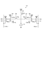
図9は、第2実施形態のプリアンプ部の詳細構成図である。
図9において、図4の第1実施形態と同様の部分には、同一の符号を付すものとする。
[第2実施形態のコンパレータ部の詳細構成]
図9は、第2実施形態のプリアンプ部の詳細構成図である。
図9において、図4の第1実施形態と同様の部分には、同一の符号を付すものとする。
第2実施形態のプリアンプ部13Cが第1実施形態のプリアンプ部13と異なる点は、NチャネルMOSトランジスタTR17及び閾値判定回路21に代えてダイオードとして機能するNチャネルMOSトランジスタTR51を備えた点である。
上記構成において、NチャネルMOSトランジスタTR51は、PチャネルMOSトランジスタTR14のドレイン端子D及び抵抗R1の接続点CP11にドレイン端子Dが接続され、PチャネルMOSトランジスタTR16のドレイン端子D及び抵抗R2の接続点CP12にソース端子Sが接続され、ゲート端子Gが接続点CP11に接続されている。
画素信号SVSLの電圧と閾値電圧信号Sthの電圧との差が大きく、第1出力信号OUTPと第2出力信号OUTNとの差分が大きい場合はNチャネルMOSトランジスタTR51がオン状態(導通状態)となり、第1出力信号OUTPと第2出力信号OUTNとの差分電圧をNチャネルMOSトランジスタTR51のダイオードとしての閾値電圧まで小さくすることが可能となる。この方式では第1実施形態と比較して、過大入力判定の比較時間や逐次変換ロジック部15からのフィードバック信号が不要となる。
また過大入力は画素信号SVSL側からしか印加されないため、ダイオードとして機能するNチャネルMOSトランジスタTR51のゲート端子Gが画素信号SVSL側に接続されていることも特徴の1つである。
ただし、負荷容量を合わせるために、TR51と同様のNチャネルMOSトランジスタをCP12側ゲート、ドレインを接続、CP11側にソースを接続することも可能である。
ただし、負荷容量を合わせるために、TR51と同様のNチャネルMOSトランジスタをCP12側ゲート、ドレインを接続、CP11側にソースを接続することも可能である。
[第2実施形態の第1変形例のコンパレータ部の詳細構成]
図10は、第2実施形態の第1変形例のプリアンプ部の詳細構成図である。
図10において、図4の第1実施形態と同様の部分には、同一の符号を付すものとする。
第2実施形態のプリアンプ部13Dが第1実施形態のプリアンプ部13と異なる点は、NチャネルMOSトランジスタTR17及び閾値判定回路14に代えてダイオードとして機能するNチャネルMOSトランジスタTR52を備えた点である。
図10は、第2実施形態の第1変形例のプリアンプ部の詳細構成図である。
図10において、図4の第1実施形態と同様の部分には、同一の符号を付すものとする。
第2実施形態のプリアンプ部13Dが第1実施形態のプリアンプ部13と異なる点は、NチャネルMOSトランジスタTR17及び閾値判定回路14に代えてダイオードとして機能するNチャネルMOSトランジスタTR52を備えた点である。
上記構成において、NチャネルMOSトランジスタTR52は、PチャネルMOSトランジスタTR13のドレイン端子D及びPチャネルMOSトランジスタTR14のソース端子Sの接続点CP1にドレイン端子Dが接続され、PチャネルMOSトランジスタTR15のドレイン端子D及びPチャネルMOSトランジスタTR16のソース端子Sの接続点CP2にソース端子Sが接続され、ゲート端子Gが接続点CP1に接続されている。
上記構成によれば、画素信号SVSLの電圧と閾値電圧信号Sthの電圧との差が大きく、第1出力信号OUTPと第2出力信号OUTNとの差分が大きい場合はNチャネルMOSトランジスタTR52がオン状態(導通状態)となり、第1出力信号OUTPと第2出力信号OUTNとの差分電圧を小さくすることが可能となる。この方式では第1実施形態と比較して、閾値判定の比較時間や逐次変換ロジック部15からのフィードバック信号が不要となる。
この場合においても、第2実施形態と同様に、過大入力は画素信号SVSL側からしか印加されないため、ダイオードとして機能するNチャネルMOSトランジスタTR52のゲート端子Gが画素信号SVSL側に接続されていることも特徴の1つである。
ただし、負荷容量を合わせるために、TR52と同様のNチャネルMOSトランジスタをCP2側ゲート、ドレインを接続、CP1側にソースを接続することも可能である。
ただし、負荷容量を合わせるために、TR52と同様のNチャネルMOSトランジスタをCP2側ゲート、ドレインを接続、CP1側にソースを接続することも可能である。
[第2実施形態の第2変形例]
以上の説明においては、プリアンプ部13Cの入力段のMOSトランジスタの構成をPチャネルMOSトランジスタ構成としていたが、NチャネルMOSトランジスタ構成を採るようにすることも可能である。
以上の説明においては、プリアンプ部13Cの入力段のMOSトランジスタの構成をPチャネルMOSトランジスタ構成としていたが、NチャネルMOSトランジスタ構成を採るようにすることも可能である。
(3)第3実施形態
[第3実施形態のコンパレータ部の詳細構成]
図11は、第3実施形態のプリアンプ部の詳細構成図である。
図11において、図4の第1実施形態と同様の部分には、同一の符号を付すものとする。
[第3実施形態のコンパレータ部の詳細構成]
図11は、第3実施形態のプリアンプ部の詳細構成図である。
図11において、図4の第1実施形態と同様の部分には、同一の符号を付すものとする。
第3実施形態のプリアンプ部13Eが第1実施形態のプリアンプ部13と異なる点は、NチャネルMOSトランジスタTR17に代えて閾値判定回路21が出力した判別結果信号SEVに基づいて、基準画素信号変換時に相当する初期電圧VSETとしてPチャネルMOSトランジスタTR13のゲート端子Gに印加するPチャネルMOSトランジスタTR53を備えた点である。
上記構成において、PチャネルMOSトランジスタTR53は、PチャネルMOSトランジスタTR13のゲート端子Gにドレイン端子Dが接続され、閾値判定回路21の出力端子OUTP1にゲート端子Gが接続されている。
本第3実施形態によれば、画素信号SVSLの電圧が所定の過大入力状態に相当する基準比較電圧Vthよりも低くなったことを閾値判定回路21が検出した場合には、PチャネルMOSトランジスタTR53をオン状態(閉状態)とするので、プリアンプ部13EのPチャネルMOSトランジスタTR13のゲート端子Gには、初期電圧VSETが印加され、基準画素信号変換時と同様の変換を行うこととなるため、他カラムに与える影響は基準画素信号変換時と同じとなるため、CDS(Correlated Double Sampling)後の影響は小さくなり、ストリーキング量の劣化を抑制することが可能となる。
[第3実施形態の第1変形例のプリアンプ部の詳細構成]
図12は、第3実施形態の第1変形例のプリアンプ部の詳細構成図である。
図12において、図11の第3実施形態と同様の部分には、同一の符号を付すものとする。
第3実施形態の第1変形例のプリアンプ部13Fが第3実施形態のプリアンプ部13Eと異なる点は、画素信号SVSLの電圧を所定の過大入力状態に相当する基準比較電圧Vthと比較して判別結果信号SEVFをPチャネルMOSトランジスタTR53のゲート端子Gに出力する閾値判定回路30を備えた点である。
図12は、第3実施形態の第1変形例のプリアンプ部の詳細構成図である。
図12において、図11の第3実施形態と同様の部分には、同一の符号を付すものとする。
第3実施形態の第1変形例のプリアンプ部13Fが第3実施形態のプリアンプ部13Eと異なる点は、画素信号SVSLの電圧を所定の過大入力状態に相当する基準比較電圧Vthと比較して判別結果信号SEVFをPチャネルMOSトランジスタTR53のゲート端子Gに出力する閾値判定回路30を備えた点である。
本第3実施形態の第1変形例によっても、画素信号SVSLの電圧が所定の過大入力状態に相当する基準比較電圧Vthよりも小さくなった場合には、PチャネルMOSトランジスタTR53をオン状態(閉状態)とするので、プリアンプ部13FのPチャネルMOSトランジスタTR13のゲート端子Gには、初期電圧VSETが印加され、基準画素信号変換時と同様の変換を行うために、他カラムに与える影響は基準画素信号変換時と同じとなり、CDS(Correlated Double Sampling)後の影響は小さくなり、ストリーキング量の劣化を抑制することが可能となる。
ここで、上記実施形態で用いていた初期電圧設定回路の構成について簡単に説明する。
図13は、初期電圧設定回路の一例の説明図である。
初期電圧設定回路は、抵抗R3の電圧降下により電流源として機能しているPチャネルMOSトランジスタTR12のドレイン端子-ソース端子間電圧Vdsを保証するととともに、プリアンプ部13のPチャネルMOSトランジスタTR13のゲート端子Gに印加する初期値電圧VSETを規定し、設定している。
図13は、初期電圧設定回路の一例の説明図である。
初期電圧設定回路は、抵抗R3の電圧降下により電流源として機能しているPチャネルMOSトランジスタTR12のドレイン端子-ソース端子間電圧Vdsを保証するととともに、プリアンプ部13のPチャネルMOSトランジスタTR13のゲート端子Gに印加する初期値電圧VSETを規定し、設定している。
(4)第4実施形態
以上の各実施形態においては、一画素を処理するA/D変換器について説明したが、本第4実施形態は、複数画素について順次A/D変換処理を行うA/D変換器を複数備えた信号処理部の実施形態である。
以上の各実施形態においては、一画素を処理するA/D変換器について説明したが、本第4実施形態は、複数画素について順次A/D変換処理を行うA/D変換器を複数備えた信号処理部の実施形態である。
[第4実施形態の信号処理部の概要構成]
図14は、第4実施形態の信号処理部の概要構成ブロック図である。
図14に示す信号処理部4Aは、一つのA/D変換器においてそれぞれ8個の画素について時分割で処理を行う場合の例であり、図示の簡略化のため、2n個(n:自然数)設けたA/D変換器のうち、n個のA/D変換器10-1~10-nを図示している。実際においては、上に延びている画素からの出力信号ラインの上方に残りのn個のA/D変換器が配置されている。
図14は、第4実施形態の信号処理部の概要構成ブロック図である。
図14に示す信号処理部4Aは、一つのA/D変換器においてそれぞれ8個の画素について時分割で処理を行う場合の例であり、図示の簡略化のため、2n個(n:自然数)設けたA/D変換器のうち、n個のA/D変換器10-1~10-nを図示している。実際においては、上に延びている画素からの出力信号ラインの上方に残りのn個のA/D変換器が配置されている。
この場合において、A/D変換器10-1~10-nは、図2に示したA/D変換器10と同様の構成を採っており、図14においては、DA変換部12、プリアンプ部13、コンパレータ部14、逐次変換ロジック部15及びローテーションロジック部16を図示している。
各A/D変換器10-1においては、図14に示す場合、画素PX1~PX4、画素PX11~PX14、画素PX21~PX24及び画素PX31~PX34の16個の画素のうち、半分の8個の画素が割り当てられている。
具体的には、図示しているA/D変換器10-1については、画素PX1、画素PX3、画素PX11、画素PX13、画素PX21、画素PX23、画素PX31、画素PX33の8個の画素が割り当てられている。
同様に図示していないA/D変換器については、画素PX2、画素PX4、画素PX12、画素PX14、画素PX22、画素PX24、画素PX32、画素PX3の8個の画素が割り当てられている。
(第4実施形態の信号処理部の基本動作)
ここで、第4実施形態の信号処理部4Aの基本動作について説明する。
信号処理部4Aを構成しているA/D変換器10-1~10-n及び図示しないn個のA/D変換器は、同期してそれぞれ独立して処理を行っているため、A/D変換器10-1を例として基本動作を説明する。
ここで、第4実施形態の信号処理部4Aの基本動作について説明する。
信号処理部4Aを構成しているA/D変換器10-1~10-n及び図示しないn個のA/D変換器は、同期してそれぞれ独立して処理を行っているため、A/D変換器10-1を例として基本動作を説明する。
A/D変換器10-1は、例えば、1回のデータ読み出しに際し、画素PX1→画素PX3→画素PX11→画素PX13→画素PX21→画素PX23→画素PX31→画素PX33の順番で処理を行う。
すなわち、1回のデータ読み出しの第1の処理タイミングにおいては、A/D変換器10-1のDA変換部12は、ローカル参照電圧生成部11が生成した複数種類のローカル基準参照信号Srefを用い、後述の逐次変換ロジック部及びローテーションロジック部の制御下で制御データDCNTのディジタル/アナログ(D/A)変換を行って閾値電圧信号Sthをプリアンプ13に出力する。
これにより、プリアンプ部13は、画素信号入力端子TSL1から入力された画素PX1に対応する画素信号SVSL及びDA変換器12から入力された閾値電圧信号Sthを増幅し、コンパレータ部14に出力する。
コンパレータ部14は、プリアンプ出力を比較し、比較結果データDCMPを逐次変換ロジック部15に出力する。
逐次変換ロジック部15は、比較結果データDCMPをアナログ/ディジタル変換時の逐次変換制御を行うための逐次変換制御データDSARを出力するとともに、入力された比較結果データDCMPを記憶し、記憶した比較結果データDCMPに基づいて画素信号SVSLのアナログ/ディジタル(A/D)変換結果である画素データDVSLを出力端子TDOUTから出力する。
以下、同様にして、第2の処理タイミング~第8の処理タイミングにおいて、A/D変換器10-1は、画素信号入力端子TSL2から入力された画素PX3、画素信号入力端子TSL3から入力された画素PX11、画素信号入力端子TSL4から入力された画素PX13、画素信号入力端子TSL5から入力された画素PX21、画素信号入力端子TSL6から入力された画素PX23、画素信号入力端子TSL7から入力された画素PX31、画素信号入力端子TSL8から入力された画素PX33のそれぞれに対応する画素信号SVSLのアナログ/ディジタル(A/D)変換を実施し、出力端子TDOUTから出力する処理を行う。
このとき、A/D変換器10-2~10-n及び図示しないn個のA/D変換器も同様の処理を同時並行して行う。
以上の説明のように、本第4実施形態によれば、第1実施形態の効果に加えて、A/D変換器の個数を画素別にA/D変換器を設ける場合と比較して約1/8とすることができ、信号処理部4Aの回路面積、ひいては、固体撮像素子の設置面積を小さくし、装置の小型化を図ることが可能となる。
(5)第5実施形態
図15は、本技術を適用した間接光飛行時間型距離センサの一例のブロック図である。
間接光飛行時間(Indirect-Time of Flight)型距離センサ100は、センサチップ101およびセンサチップ101に積層された回路チップ102を備えている。
図15は、本技術を適用した間接光飛行時間型距離センサの一例のブロック図である。
間接光飛行時間(Indirect-Time of Flight)型距離センサ100は、センサチップ101およびセンサチップ101に積層された回路チップ102を備えている。
画素アレイ部112は、センサチップ101上に二次元のグリッドパターンでアレイ状に配置された複数の画素(pixel)111を有している。ここで、画素アレイ部112は、行列上に配置されていても良く、また、複数の列信号線を含んでも良い。それぞれの列信号線はそれぞれの画素に接続されている。
回路チップ102には、垂直駆動回路113、カラム信号処理部114、タイミング調整回路115および出力回路116が配置されている。
回路チップ102には、垂直駆動回路113、カラム信号処理部114、タイミング調整回路115および出力回路116が配置されている。
垂直駆動回路113は、画素を駆動し、カラム信号処理部114に画素信号を出力するように構成されている。
カラム信号処理部114は、入力された画素信号に対して、A/D変換処理を実施し、A/D変換処理した画素データを出力回路116に出力する。
出力回路116は、カラム信号処理部114からの画素データに対して、CDS(Correlated Double Sampling)処理などを実行し、後段の信号処理回路に画素データを出力する。
カラム信号処理部114は、入力された画素信号に対して、A/D変換処理を実施し、A/D変換処理した画素データを出力回路116に出力する。
出力回路116は、カラム信号処理部114からの画素データに対して、CDS(Correlated Double Sampling)処理などを実行し、後段の信号処理回路に画素データを出力する。
タイミング制御回路115は、それぞれの垂直駆動回路113の駆動タイミングを制御するように構成されている。カラム信号処理部114、出力回路116は、タイミング制御回路115が出力した垂直同期信号と同期して動作している。
ここで、画素アレイ部112を構成している画素111について詳細に説明する。
図16は、本技術の形態における画素の一構成例を示す回路図である。
画素アレイ部112には、二次元状のグリッドパターンで複数の画素111が配置されており、それぞれの画素111は赤外光を受光し、画素信号に光電変換可能な構成となっている。
図16は、本技術の形態における画素の一構成例を示す回路図である。
画素アレイ部112には、二次元状のグリッドパターンで複数の画素111が配置されており、それぞれの画素111は赤外光を受光し、画素信号に光電変換可能な構成となっている。
また、画素111の列ごとに、垂直方向に垂直信号線VSL1及び垂直信号線VSL2が配線される。画素アレイ部112内の列の総数をM(Mは、整数)とすると、合計で2×M本の垂直信号線が配線される。それぞれの画素において、2つのタップを有している。垂直信号線VSL1は画素111のタップAに接続され、垂直信号線VSL2は画素111のタップBに接続される。また、垂直信号線VSL1は、画素信号AINP1を伝送し、垂直信号線VSL2は、画素信号AINP2を伝送する。
垂直駆動回路113は、画素エリア112の行を順に選択して駆動し、その行において画素ブロック221ごとに画素信号AINP1および画素信号AINP2を同時に出力させる。言い換えれば、垂直駆動回路113は、画素111の2k行目および2k+1行目を同時に駆動する。
画素111は、フォトダイオード121、二つの転送トランジスタ122、123、二つのリセットトランジスタ124、125、2つのタップ(浮遊拡散層126、127)、二つの増幅トランジスタ128、129及び二つの選択トランジスタ130、131を備える。
フォトダイオード121は、受光した光を光電変換して電荷を生成するものである。このフォトダイオード121は、半導体基板において回路を配置する面を表面として、表面に対する裏面に配置される。このような固体撮像素子は、裏面照射型の固体撮像素子と呼ばれる。なお、裏面照射型の代わりに、表面にフォトダイオード121を配置する表面照射型の構成を用いることもできる。
転送トランジスタ122及び転送トランジスタ123は、垂直駆動回路113からの転送信号TRGに従ってフォトダイオード121からTAPA126、TAPB127にそれぞれシーケンシャルに電荷を転送するものである。
TAPA126およびTAPB127は、転送された電荷を蓄積して、蓄積した電荷の量に応じた電圧を生成するものである。
TAPA126およびTAPB127は、転送された電荷を蓄積して、蓄積した電荷の量に応じた電圧を生成するものである。
オーバーフロートランジスタ132は、フォトダイオード121の電荷をシーケンシャルに高電位側電源VDDに排出するトランジスタで、フォトダイオード121をリセットする機能を持つ。
リセットトランジスタ124、125は、垂直駆動回路113からのリセット信号RSTpに従ってTAPA126、TAPB127のそれぞれから電荷を引き抜いて、電荷量を初期化するものである。
増幅トランジスタ128、129は、TAPA126、TAPB127の電圧をそれぞれ増幅するものである。選択トランジスタ130、131は、垂直駆動回路113からの選択信号SELpに従って、増幅された電圧の信号を画素信号としてふたつの垂直信号線(例えば、VSL1、VSL2)を介してカラム信号処理部114へ出力するものである。垂直信号線および垂直信号線VSL2は、カラム信号処理部114内の一つのA/D変換器10の入力に接続されている。
なお、画素111の回路構成は、光電変換により画素信号を生成することができるものであれば、図15に例示した構成に限定されない。
本第5実施形態によれば、第4実施形態と同様に、固体撮像素子の設置面積を小さくし、間接光飛行時間型距離センサの小型化を図ることが可能となる。
なお、本明細書に記載された効果はあくまで例示であって限定されるものでは無く、また他の効果があってもよい。
なお、本技術は以下のような構成も採ることができる。
(1)
画素信号の過大入力が入力されたかどうか判断する閾値電圧の比較を行う比較器回路と、
前記比較の結果が制御端子に入力され、クランプ回路を構成する第1のトランジスタと、
を備えたA/D変換器。
(2)
クランプ時に接続される第1の所定位置と第2の所定位置に流れる電流を等しくし、あるいは、前記第1の所定位置と前記第2の所定位置の電圧を等しくする、
(1)記載のA/D変換器。
(3)
入力電流ライン及び参照電流ラインを構成する一対の差動対トランジスタと、
前記差動対トランジスタに流すバイアス電流を制御する一対のバイアストランジスタと、を有し、
前記第1のトランジスタは、前記一対のバイアストランジスタに対し、上流側あるいは下流側のいずれかに設けられている、
(1)又は(2)記載のA/D変換器。
(4)
前記クランプ回路は、前記画素信号として所定の過大入力閾値以上の信号が入力されたか否かを判定する閾値判定回路を備え、
前記閾値判定回路の出力に基づいて、前記第1のトランジスタは、クランプ時に接続される第1の所定位置と第2の所定位置とを短絡状態とする、
(1)~(3)のいずれか1つに記載のA/D変換器。
(5)
入力電流ライン及び参照電流ラインを構成する一対の差動対トランジスタと、
前記差動対トランジスタに流すバイアス電流を制御する一対のバイアストランジスタと、
クランプ時に接続すべき第1の所定位置と第2の所定位置に対し、前記第1の所定位置にアノードが接続され、前記第2の所定位置にカソードが接続されたダイオードを備える、
A/D変換器。
(6)
光電変換を行う複数の画素がアレイ状に配置された画素アレイ部と、
前記画素アレイ部からアナログ画素信号を読み出して信号処理を行う信号処理部と、を備え、
前記信号処理部は、前記アナログ画素信号のアナログ/ディジタル変換を行うA/D変換器を含み、
前記A/D変換器は、画素信号と過大入力が入力されたかどうか判断する閾値電圧の比較を行う比較器回路と、
前記比較の結果が制御端子として入力され、クランプ回路を構成する第1のトランジスタと、
を備えた電子機器。
(7)
光電変換を行う複数の画素がアレイ状に配置された画素アレイ部と、
前記画素アレイ部からアナログ画素信号を読み出して信号処理を行う信号処理部と、を備え、
前記信号処理部は、前記アナログ画素信号のアナログ/ディジタル変換を行うA/D変換器を含み、
前記A/D変換器は、入力電流ライン及び参照電流ラインを構成する一対の差動対トランジスタと、
前記差動対トランジスタに流すバイアス電流を制御する一対のバイアストランジスタと、
クランプ時に接続すべき第1の所定位置と第2の所定位置に対し、前記第1の所定位置にアノードが接続され、前記第2の所定位置にカソードが接続されたダイオードと、
を備えた電子機器。
(1)
画素信号の過大入力が入力されたかどうか判断する閾値電圧の比較を行う比較器回路と、
前記比較の結果が制御端子に入力され、クランプ回路を構成する第1のトランジスタと、
を備えたA/D変換器。
(2)
クランプ時に接続される第1の所定位置と第2の所定位置に流れる電流を等しくし、あるいは、前記第1の所定位置と前記第2の所定位置の電圧を等しくする、
(1)記載のA/D変換器。
(3)
入力電流ライン及び参照電流ラインを構成する一対の差動対トランジスタと、
前記差動対トランジスタに流すバイアス電流を制御する一対のバイアストランジスタと、を有し、
前記第1のトランジスタは、前記一対のバイアストランジスタに対し、上流側あるいは下流側のいずれかに設けられている、
(1)又は(2)記載のA/D変換器。
(4)
前記クランプ回路は、前記画素信号として所定の過大入力閾値以上の信号が入力されたか否かを判定する閾値判定回路を備え、
前記閾値判定回路の出力に基づいて、前記第1のトランジスタは、クランプ時に接続される第1の所定位置と第2の所定位置とを短絡状態とする、
(1)~(3)のいずれか1つに記載のA/D変換器。
(5)
入力電流ライン及び参照電流ラインを構成する一対の差動対トランジスタと、
前記差動対トランジスタに流すバイアス電流を制御する一対のバイアストランジスタと、
クランプ時に接続すべき第1の所定位置と第2の所定位置に対し、前記第1の所定位置にアノードが接続され、前記第2の所定位置にカソードが接続されたダイオードを備える、
A/D変換器。
(6)
光電変換を行う複数の画素がアレイ状に配置された画素アレイ部と、
前記画素アレイ部からアナログ画素信号を読み出して信号処理を行う信号処理部と、を備え、
前記信号処理部は、前記アナログ画素信号のアナログ/ディジタル変換を行うA/D変換器を含み、
前記A/D変換器は、画素信号と過大入力が入力されたかどうか判断する閾値電圧の比較を行う比較器回路と、
前記比較の結果が制御端子として入力され、クランプ回路を構成する第1のトランジスタと、
を備えた電子機器。
(7)
光電変換を行う複数の画素がアレイ状に配置された画素アレイ部と、
前記画素アレイ部からアナログ画素信号を読み出して信号処理を行う信号処理部と、を備え、
前記信号処理部は、前記アナログ画素信号のアナログ/ディジタル変換を行うA/D変換器を含み、
前記A/D変換器は、入力電流ライン及び参照電流ラインを構成する一対の差動対トランジスタと、
前記差動対トランジスタに流すバイアス電流を制御する一対のバイアストランジスタと、
クランプ時に接続すべき第1の所定位置と第2の所定位置に対し、前記第1の所定位置にアノードが接続され、前記第2の所定位置にカソードが接続されたダイオードと、
を備えた電子機器。
2 画素アレイ部
4 信号処理部
10 A/D変換器
11 ローカル参照電圧生成部
12 DA変換部
13、13A~13F プリアンプ部
14 コンパレータ部
14A 増幅部
14B ラッチ部
15 逐次変換ロジック部
16 ローテーションロジック部 21 閾値判定回路 CP1、CP11 接続点(第1の所定位置)
CP2、CP12 接続点(第2の所定位置)
TR17、TR17A、TR17B NチャネルMOSトランジスタ(クランプ回路)
TR51、TR52 NチャネルMOSトランジスタ(クランプ回路)
TR53 PチャネルMOSトランジスタ(スイッチング素子)
DA 差動アンプ
SEV 判別結果信号
4 信号処理部
10 A/D変換器
11 ローカル参照電圧生成部
12 DA変換部
13、13A~13F プリアンプ部
14 コンパレータ部
14A 増幅部
14B ラッチ部
15 逐次変換ロジック部
16 ローテーションロジック部 21 閾値判定回路 CP1、CP11 接続点(第1の所定位置)
CP2、CP12 接続点(第2の所定位置)
TR17、TR17A、TR17B NチャネルMOSトランジスタ(クランプ回路)
TR51、TR52 NチャネルMOSトランジスタ(クランプ回路)
TR53 PチャネルMOSトランジスタ(スイッチング素子)
DA 差動アンプ
SEV 判別結果信号
Claims (6)
- 画素信号の過大入力が入力されたかどうか判断する閾値電圧の比較を行う比較器回路と、
前記比較の結果が制御端子に入力され、クランプ回路を構成する第1のトランジスタと、
を備えたA/D変換器。 - クランプ時に接続される第1の所定位置と第2の所定位置に流れる電流を等しくし、あるいは、前記第1の所定位置と前記第2の所定位置の電圧を等しくする、
請求項1記載のA/D変換器。 - 入力電流ライン及び参照電流ラインを構成する一対の差動対トランジスタと、
前記差動対トランジスタに流すバイアス電流を制御する一対のバイアストランジスタと、を有し、
前記第1のトランジスタは、前記一対のバイアストランジスタに対し、上流側あるいは下流側のいずれかに設けられている、
請求項2記載のA/D変換器。 - 前記クランプ回路は、前記画素信号として所定の過大入力閾値以上の信号が入力されたか否かを判定する閾値判定回路を備え、
前記閾値判定回路の出力に基づいて、前記第1のトランジスタは、クランプ時に接続される第1の所定位置と第2の所定位置とを短絡状態とする、
請求項1記載のA/D変換器。 - 入力電流ライン及び参照電流ラインを構成する一対の差動対トランジスタと、
前記差動対トランジスタに流すバイアス電流を制御する一対のバイアストランジスタと、
クランプ時に接続すべき第1の所定位置と第2の所定位置に対し、前記第1の所定位置にアノードが接続され、前記第2の所定位置にカソードが接続されたダイオードを備える、
A/D変換器。 - 光電変換を行う複数の画素がアレイ状に配置された画素アレイ部と、
前記画素アレイ部からアナログ画素信号を読み出して信号処理を行う信号処理部と、を備え、
前記信号処理部は、前記アナログ画素信号のアナログ/ディジタル変換を行うA/D変換器を含み、
前記A/D変換器は、画素信号と過大入力が入力されたかどうか判断する閾値電圧の比較を行う比較器回路と、
前記比較の結果が制御端子として入力され、クランプ回路を構成する第1のトランジスタと、
を備えた電子機器。
Priority Applications (4)
| Application Number | Priority Date | Filing Date | Title |
|---|---|---|---|
| CN201980067151.XA CN112997476B (zh) | 2018-10-24 | 2019-10-02 | A/d转换器和电子设备 |
| US17/273,570 US11283460B2 (en) | 2018-10-24 | 2019-10-02 | A/D converter and electronic equipment |
| DE112019005341.8T DE112019005341T5 (de) | 2018-10-24 | 2019-10-02 | A/d-wandler und elektronisches gerät |
| JP2020553031A JP7464531B2 (ja) | 2018-10-24 | 2019-10-02 | A/d変換器及び電子機器 |
Applications Claiming Priority (2)
| Application Number | Priority Date | Filing Date | Title |
|---|---|---|---|
| JP2018-200376 | 2018-10-24 | ||
| JP2018200376 | 2018-10-24 |
Publications (1)
| Publication Number | Publication Date |
|---|---|
| WO2020085016A1 true WO2020085016A1 (ja) | 2020-04-30 |
Family
ID=70330690
Family Applications (1)
| Application Number | Title | Priority Date | Filing Date |
|---|---|---|---|
| PCT/JP2019/038839 Ceased WO2020085016A1 (ja) | 2018-10-24 | 2019-10-02 | A/d変換器及び電子機器 |
Country Status (6)
| Country | Link |
|---|---|
| US (1) | US11283460B2 (ja) |
| JP (1) | JP7464531B2 (ja) |
| CN (1) | CN112997476B (ja) |
| DE (1) | DE112019005341T5 (ja) |
| TW (1) | TWI835869B (ja) |
| WO (1) | WO2020085016A1 (ja) |
Cited By (2)
| Publication number | Priority date | Publication date | Assignee | Title |
|---|---|---|---|---|
| US20150371280A1 (en) * | 2014-06-24 | 2015-12-24 | Arris Enterprises, Inc. | Tracking ad preferences in adaptive bit rate systems |
| WO2022074940A1 (ja) * | 2020-10-08 | 2022-04-14 | ソニーセミコンダクタソリューションズ株式会社 | 固体撮像素子、および、撮像装置 |
Families Citing this family (1)
| Publication number | Priority date | Publication date | Assignee | Title |
|---|---|---|---|---|
| US10735683B1 (en) * | 2019-04-09 | 2020-08-04 | Obsidian Sensors, Inc. | Systems and methods for low-power image digitization |
Citations (3)
| Publication number | Priority date | Publication date | Assignee | Title |
|---|---|---|---|---|
| JP2005252529A (ja) * | 2004-03-03 | 2005-09-15 | Sony Corp | 固体撮像装置、画素信号読出方法 |
| WO2013038958A1 (ja) * | 2011-09-12 | 2013-03-21 | シャープ株式会社 | クランプ回路及びそれを用いた信号処理システム |
| JP2013172270A (ja) * | 2012-02-20 | 2013-09-02 | Sony Corp | 比較器、ad変換器、固体撮像装置、カメラシステム、および電子機器 |
Family Cites Families (4)
| Publication number | Priority date | Publication date | Assignee | Title |
|---|---|---|---|---|
| JP4650445B2 (ja) * | 2007-04-02 | 2011-03-16 | ソニー株式会社 | クランプ信号生成装置およびクランプ信号生成方法 |
| US20090021623A1 (en) * | 2007-07-18 | 2009-01-22 | Micron Technology, Inc. | Systems, methods and devices for a CMOS imager having a pixel output clamp |
| JP2010220111A (ja) * | 2009-03-18 | 2010-09-30 | Toshiba Corp | クランプ回路およびそれを備えた固体撮像装置 |
| JP6407083B2 (ja) * | 2015-03-30 | 2018-10-17 | キヤノン株式会社 | 光電変換装置、および、光電変換システム |
-
2019
- 2019-09-26 TW TW108134764A patent/TWI835869B/zh active
- 2019-10-02 WO PCT/JP2019/038839 patent/WO2020085016A1/ja not_active Ceased
- 2019-10-02 US US17/273,570 patent/US11283460B2/en active Active
- 2019-10-02 CN CN201980067151.XA patent/CN112997476B/zh active Active
- 2019-10-02 JP JP2020553031A patent/JP7464531B2/ja active Active
- 2019-10-02 DE DE112019005341.8T patent/DE112019005341T5/de active Granted
Patent Citations (3)
| Publication number | Priority date | Publication date | Assignee | Title |
|---|---|---|---|---|
| JP2005252529A (ja) * | 2004-03-03 | 2005-09-15 | Sony Corp | 固体撮像装置、画素信号読出方法 |
| WO2013038958A1 (ja) * | 2011-09-12 | 2013-03-21 | シャープ株式会社 | クランプ回路及びそれを用いた信号処理システム |
| JP2013172270A (ja) * | 2012-02-20 | 2013-09-02 | Sony Corp | 比較器、ad変換器、固体撮像装置、カメラシステム、および電子機器 |
Cited By (4)
| Publication number | Priority date | Publication date | Assignee | Title |
|---|---|---|---|---|
| US20150371280A1 (en) * | 2014-06-24 | 2015-12-24 | Arris Enterprises, Inc. | Tracking ad preferences in adaptive bit rate systems |
| US11869038B2 (en) * | 2014-06-24 | 2024-01-09 | Arris Enterprises Llc | Tracking ad preferences in adaptive bit rate systems |
| WO2022074940A1 (ja) * | 2020-10-08 | 2022-04-14 | ソニーセミコンダクタソリューションズ株式会社 | 固体撮像素子、および、撮像装置 |
| US12356100B2 (en) | 2020-10-08 | 2025-07-08 | Sony Semiconductor Solutions Corporation | Solid-state imaging element and imaging apparatus |
Also Published As
| Publication number | Publication date |
|---|---|
| US20210258017A1 (en) | 2021-08-19 |
| DE112019005341T5 (de) | 2021-08-26 |
| JPWO2020085016A1 (ja) | 2021-09-30 |
| CN112997476A (zh) | 2021-06-18 |
| TW202023266A (zh) | 2020-06-16 |
| TWI835869B (zh) | 2024-03-21 |
| CN112997476B (zh) | 2024-12-17 |
| US11283460B2 (en) | 2022-03-22 |
| JP7464531B2 (ja) | 2024-04-09 |
Similar Documents
| Publication | Publication Date | Title |
|---|---|---|
| JP7531390B2 (ja) | 固体撮像装置、ad変換回路および電流補償回路 | |
| CN110121037A (zh) | 具有双重转换增益读出的图像传感器 | |
| JP2012160845A (ja) | 撮像装置 | |
| US10728483B2 (en) | Comparator with correlated double sampling scheme, CMOS image sensor including the same, and operating method thereof | |
| US11303836B2 (en) | Solid-state imaging device and electronic equipment | |
| JP6794985B2 (ja) | 固体撮像装置および固体撮像装置の駆動方法 | |
| CN113301279A (zh) | 图像传感器和包括图像传感器的成像设备 | |
| US10447957B2 (en) | Unit pixel and operating method thereof and CMOS image sensor using the same | |
| JP7464531B2 (ja) | A/d変換器及び電子機器 | |
| WO2012144218A1 (ja) | 固体撮像装置および固体撮像装置の駆動方法 | |
| TW202508300A (zh) | 分散式斜坡線性補償電路 | |
| CN109906605B (zh) | 摄像装置和电子设备 | |
| TWI840395B (zh) | 固態攝像元件及電子機器 | |
| CN116132836A (zh) | 使用输出电压限幅的模数转换电路及其操作方法 | |
| US8587689B2 (en) | Time AD converter and solid state image pickup device | |
| KR20230071033A (ko) | 출력 전압 클리핑을 이용하는 아날로그 디지털 변환 회로 및 그것의 동작 방법 | |
| US10715758B2 (en) | Amplification circuit performing primary and secondary amplifications | |
| KR102955180B1 (ko) | 판단 지연을 감소시키기 위한 아날로그 디지털 변환 회로 및 그것의 동작 방법 | |
| TW202322574A (zh) | 類比數位轉換電路 | |
| JP2023159864A (ja) | 判定遅延を減少させるためのアナログ-デジタル変換回路およびその動作方法 | |
| TW202322618A (zh) | 類比數位轉換電路及其操作方法 | |
| CN116132835A (zh) | 使用自动调零时段优化的模数转换电路及其操作方法 | |
| KR20230149690A (ko) | 판단 지연을 감소시키기 위한 아날로그 디지털 변환 회로 및 그것의 동작 방법 | |
| KR20230071039A (ko) | 오토 제로 구간 최적화를 이용하는 아날로그 디지털 변환 회로 및 그것의 동작 방법 | |
| CN116170706A (zh) | 用于优化双转换增益操作的模数转换电路及其操作方法 |
Legal Events
| Date | Code | Title | Description |
|---|---|---|---|
| 121 | Ep: the epo has been informed by wipo that ep was designated in this application |
Ref document number: 19875631 Country of ref document: EP Kind code of ref document: A1 |
|
| ENP | Entry into the national phase |
Ref document number: 2020553031 Country of ref document: JP Kind code of ref document: A |
|
| 122 | Ep: pct application non-entry in european phase |
Ref document number: 19875631 Country of ref document: EP Kind code of ref document: A1 |