WO2020071357A1 - 接合構造体の製造方法 - Google Patents
接合構造体の製造方法Info
- Publication number
- WO2020071357A1 WO2020071357A1 PCT/JP2019/038727 JP2019038727W WO2020071357A1 WO 2020071357 A1 WO2020071357 A1 WO 2020071357A1 JP 2019038727 W JP2019038727 W JP 2019038727W WO 2020071357 A1 WO2020071357 A1 WO 2020071357A1
- Authority
- WO
- WIPO (PCT)
- Prior art keywords
- reflow
- pressure
- solder
- test
- atmosphere
- Prior art date
Links
Images

Classifications
-
- B—PERFORMING OPERATIONS; TRANSPORTING
- B23—MACHINE TOOLS; METAL-WORKING NOT OTHERWISE PROVIDED FOR
- B23K—SOLDERING OR UNSOLDERING; WELDING; CLADDING OR PLATING BY SOLDERING OR WELDING; CUTTING BY APPLYING HEAT LOCALLY, e.g. FLAME CUTTING; WORKING BY LASER BEAM
- B23K1/00—Soldering, e.g. brazing, or unsoldering
- B23K1/008—Soldering within a furnace
-
- B—PERFORMING OPERATIONS; TRANSPORTING
- B23—MACHINE TOOLS; METAL-WORKING NOT OTHERWISE PROVIDED FOR
- B23K—SOLDERING OR UNSOLDERING; WELDING; CLADDING OR PLATING BY SOLDERING OR WELDING; CUTTING BY APPLYING HEAT LOCALLY, e.g. FLAME CUTTING; WORKING BY LASER BEAM
- B23K1/00—Soldering, e.g. brazing, or unsoldering
- B23K1/0008—Soldering, e.g. brazing, or unsoldering specially adapted for particular articles or work
- B23K1/0016—Brazing of electronic components
-
- H—ELECTRICITY
- H01—ELECTRIC ELEMENTS
- H01L—SEMICONDUCTOR DEVICES NOT COVERED BY CLASS H10
- H01L24/00—Arrangements for connecting or disconnecting semiconductor or solid-state bodies; Methods or apparatus related thereto
- H01L24/01—Means for bonding being attached to, or being formed on, the surface to be connected, e.g. chip-to-package, die-attach, "first-level" interconnects; Manufacturing methods related thereto
- H01L24/10—Bump connectors ; Manufacturing methods related thereto
- H01L24/11—Manufacturing methods
-
- H—ELECTRICITY
- H01—ELECTRIC ELEMENTS
- H01L—SEMICONDUCTOR DEVICES NOT COVERED BY CLASS H10
- H01L24/00—Arrangements for connecting or disconnecting semiconductor or solid-state bodies; Methods or apparatus related thereto
- H01L24/01—Means for bonding being attached to, or being formed on, the surface to be connected, e.g. chip-to-package, die-attach, "first-level" interconnects; Manufacturing methods related thereto
- H01L24/10—Bump connectors ; Manufacturing methods related thereto
- H01L24/12—Structure, shape, material or disposition of the bump connectors prior to the connecting process
- H01L24/13—Structure, shape, material or disposition of the bump connectors prior to the connecting process of an individual bump connector
-
- H—ELECTRICITY
- H01—ELECTRIC ELEMENTS
- H01L—SEMICONDUCTOR DEVICES NOT COVERED BY CLASS H10
- H01L24/00—Arrangements for connecting or disconnecting semiconductor or solid-state bodies; Methods or apparatus related thereto
- H01L24/80—Methods for connecting semiconductor or other solid state bodies using means for bonding being attached to, or being formed on, the surface to be connected
- H01L24/81—Methods for connecting semiconductor or other solid state bodies using means for bonding being attached to, or being formed on, the surface to be connected using a bump connector
-
- H—ELECTRICITY
- H05—ELECTRIC TECHNIQUES NOT OTHERWISE PROVIDED FOR
- H05K—PRINTED CIRCUITS; CASINGS OR CONSTRUCTIONAL DETAILS OF ELECTRIC APPARATUS; MANUFACTURE OF ASSEMBLAGES OF ELECTRICAL COMPONENTS
- H05K3/00—Apparatus or processes for manufacturing printed circuits
- H05K3/30—Assembling printed circuits with electric components, e.g. with resistor
- H05K3/32—Assembling printed circuits with electric components, e.g. with resistor electrically connecting electric components or wires to printed circuits
- H05K3/34—Assembling printed circuits with electric components, e.g. with resistor electrically connecting electric components or wires to printed circuits by soldering
- H05K3/3494—Heating methods for reflowing of solder
-
- B—PERFORMING OPERATIONS; TRANSPORTING
- B23—MACHINE TOOLS; METAL-WORKING NOT OTHERWISE PROVIDED FOR
- B23K—SOLDERING OR UNSOLDERING; WELDING; CLADDING OR PLATING BY SOLDERING OR WELDING; CUTTING BY APPLYING HEAT LOCALLY, e.g. FLAME CUTTING; WORKING BY LASER BEAM
- B23K2101/00—Articles made by soldering, welding or cutting
- B23K2101/36—Electric or electronic devices
- B23K2101/42—Printed circuits
-
- H—ELECTRICITY
- H01—ELECTRIC ELEMENTS
- H01L—SEMICONDUCTOR DEVICES NOT COVERED BY CLASS H10
- H01L2224/00—Indexing scheme for arrangements for connecting or disconnecting semiconductor or solid-state bodies and methods related thereto as covered by H01L24/00
- H01L2224/01—Means for bonding being attached to, or being formed on, the surface to be connected, e.g. chip-to-package, die-attach, "first-level" interconnects; Manufacturing methods related thereto
- H01L2224/02—Bonding areas; Manufacturing methods related thereto
- H01L2224/04—Structure, shape, material or disposition of the bonding areas prior to the connecting process
- H01L2224/0401—Bonding areas specifically adapted for bump connectors, e.g. under bump metallisation [UBM]
-
- H—ELECTRICITY
- H01—ELECTRIC ELEMENTS
- H01L—SEMICONDUCTOR DEVICES NOT COVERED BY CLASS H10
- H01L2224/00—Indexing scheme for arrangements for connecting or disconnecting semiconductor or solid-state bodies and methods related thereto as covered by H01L24/00
- H01L2224/01—Means for bonding being attached to, or being formed on, the surface to be connected, e.g. chip-to-package, die-attach, "first-level" interconnects; Manufacturing methods related thereto
- H01L2224/02—Bonding areas; Manufacturing methods related thereto
- H01L2224/04—Structure, shape, material or disposition of the bonding areas prior to the connecting process
- H01L2224/05—Structure, shape, material or disposition of the bonding areas prior to the connecting process of an individual bonding area
- H01L2224/05001—Internal layers
- H01L2224/05073—Single internal layer
-
- H—ELECTRICITY
- H01—ELECTRIC ELEMENTS
- H01L—SEMICONDUCTOR DEVICES NOT COVERED BY CLASS H10
- H01L2224/00—Indexing scheme for arrangements for connecting or disconnecting semiconductor or solid-state bodies and methods related thereto as covered by H01L24/00
- H01L2224/01—Means for bonding being attached to, or being formed on, the surface to be connected, e.g. chip-to-package, die-attach, "first-level" interconnects; Manufacturing methods related thereto
- H01L2224/02—Bonding areas; Manufacturing methods related thereto
- H01L2224/04—Structure, shape, material or disposition of the bonding areas prior to the connecting process
- H01L2224/05—Structure, shape, material or disposition of the bonding areas prior to the connecting process of an individual bonding area
- H01L2224/05001—Internal layers
- H01L2224/05099—Material
- H01L2224/051—Material with a principal constituent of the material being a metal or a metalloid, e.g. boron [B], silicon [Si], germanium [Ge], arsenic [As], antimony [Sb], tellurium [Te] and polonium [Po], and alloys thereof
- H01L2224/05138—Material with a principal constituent of the material being a metal or a metalloid, e.g. boron [B], silicon [Si], germanium [Ge], arsenic [As], antimony [Sb], tellurium [Te] and polonium [Po], and alloys thereof the principal constituent melting at a temperature of greater than or equal to 950°C and less than 1550°C
- H01L2224/05155—Nickel [Ni] as principal constituent
-
- H—ELECTRICITY
- H01—ELECTRIC ELEMENTS
- H01L—SEMICONDUCTOR DEVICES NOT COVERED BY CLASS H10
- H01L2224/00—Indexing scheme for arrangements for connecting or disconnecting semiconductor or solid-state bodies and methods related thereto as covered by H01L24/00
- H01L2224/01—Means for bonding being attached to, or being formed on, the surface to be connected, e.g. chip-to-package, die-attach, "first-level" interconnects; Manufacturing methods related thereto
- H01L2224/02—Bonding areas; Manufacturing methods related thereto
- H01L2224/04—Structure, shape, material or disposition of the bonding areas prior to the connecting process
- H01L2224/05—Structure, shape, material or disposition of the bonding areas prior to the connecting process of an individual bonding area
- H01L2224/0554—External layer
- H01L2224/05599—Material
- H01L2224/056—Material with a principal constituent of the material being a metal or a metalloid, e.g. boron [B], silicon [Si], germanium [Ge], arsenic [As], antimony [Sb], tellurium [Te] and polonium [Po], and alloys thereof
- H01L2224/05638—Material with a principal constituent of the material being a metal or a metalloid, e.g. boron [B], silicon [Si], germanium [Ge], arsenic [As], antimony [Sb], tellurium [Te] and polonium [Po], and alloys thereof the principal constituent melting at a temperature of greater than or equal to 950°C and less than 1550°C
- H01L2224/05644—Gold [Au] as principal constituent
-
- H—ELECTRICITY
- H01—ELECTRIC ELEMENTS
- H01L—SEMICONDUCTOR DEVICES NOT COVERED BY CLASS H10
- H01L2224/00—Indexing scheme for arrangements for connecting or disconnecting semiconductor or solid-state bodies and methods related thereto as covered by H01L24/00
- H01L2224/01—Means for bonding being attached to, or being formed on, the surface to be connected, e.g. chip-to-package, die-attach, "first-level" interconnects; Manufacturing methods related thereto
- H01L2224/10—Bump connectors; Manufacturing methods related thereto
- H01L2224/11—Manufacturing methods
- H01L2224/113—Manufacturing methods by local deposition of the material of the bump connector
- H01L2224/1131—Manufacturing methods by local deposition of the material of the bump connector in liquid form
- H01L2224/1132—Screen printing, i.e. using a stencil
-
- H—ELECTRICITY
- H01—ELECTRIC ELEMENTS
- H01L—SEMICONDUCTOR DEVICES NOT COVERED BY CLASS H10
- H01L2224/00—Indexing scheme for arrangements for connecting or disconnecting semiconductor or solid-state bodies and methods related thereto as covered by H01L24/00
- H01L2224/01—Means for bonding being attached to, or being formed on, the surface to be connected, e.g. chip-to-package, die-attach, "first-level" interconnects; Manufacturing methods related thereto
- H01L2224/10—Bump connectors; Manufacturing methods related thereto
- H01L2224/12—Structure, shape, material or disposition of the bump connectors prior to the connecting process
- H01L2224/13—Structure, shape, material or disposition of the bump connectors prior to the connecting process of an individual bump connector
- H01L2224/13001—Core members of the bump connector
- H01L2224/13099—Material
- H01L2224/131—Material with a principal constituent of the material being a metal or a metalloid, e.g. boron [B], silicon [Si], germanium [Ge], arsenic [As], antimony [Sb], tellurium [Te] and polonium [Po], and alloys thereof
- H01L2224/13101—Material with a principal constituent of the material being a metal or a metalloid, e.g. boron [B], silicon [Si], germanium [Ge], arsenic [As], antimony [Sb], tellurium [Te] and polonium [Po], and alloys thereof the principal constituent melting at a temperature of less than 400°C
- H01L2224/13109—Indium [In] as principal constituent
-
- H—ELECTRICITY
- H01—ELECTRIC ELEMENTS
- H01L—SEMICONDUCTOR DEVICES NOT COVERED BY CLASS H10
- H01L2224/00—Indexing scheme for arrangements for connecting or disconnecting semiconductor or solid-state bodies and methods related thereto as covered by H01L24/00
- H01L2224/01—Means for bonding being attached to, or being formed on, the surface to be connected, e.g. chip-to-package, die-attach, "first-level" interconnects; Manufacturing methods related thereto
- H01L2224/10—Bump connectors; Manufacturing methods related thereto
- H01L2224/12—Structure, shape, material or disposition of the bump connectors prior to the connecting process
- H01L2224/13—Structure, shape, material or disposition of the bump connectors prior to the connecting process of an individual bump connector
- H01L2224/13001—Core members of the bump connector
- H01L2224/13099—Material
- H01L2224/131—Material with a principal constituent of the material being a metal or a metalloid, e.g. boron [B], silicon [Si], germanium [Ge], arsenic [As], antimony [Sb], tellurium [Te] and polonium [Po], and alloys thereof
- H01L2224/13101—Material with a principal constituent of the material being a metal or a metalloid, e.g. boron [B], silicon [Si], germanium [Ge], arsenic [As], antimony [Sb], tellurium [Te] and polonium [Po], and alloys thereof the principal constituent melting at a temperature of less than 400°C
- H01L2224/13111—Tin [Sn] as principal constituent
-
- H—ELECTRICITY
- H01—ELECTRIC ELEMENTS
- H01L—SEMICONDUCTOR DEVICES NOT COVERED BY CLASS H10
- H01L2224/00—Indexing scheme for arrangements for connecting or disconnecting semiconductor or solid-state bodies and methods related thereto as covered by H01L24/00
- H01L2224/01—Means for bonding being attached to, or being formed on, the surface to be connected, e.g. chip-to-package, die-attach, "first-level" interconnects; Manufacturing methods related thereto
- H01L2224/10—Bump connectors; Manufacturing methods related thereto
- H01L2224/12—Structure, shape, material or disposition of the bump connectors prior to the connecting process
- H01L2224/13—Structure, shape, material or disposition of the bump connectors prior to the connecting process of an individual bump connector
- H01L2224/13001—Core members of the bump connector
- H01L2224/13099—Material
- H01L2224/131—Material with a principal constituent of the material being a metal or a metalloid, e.g. boron [B], silicon [Si], germanium [Ge], arsenic [As], antimony [Sb], tellurium [Te] and polonium [Po], and alloys thereof
- H01L2224/13101—Material with a principal constituent of the material being a metal or a metalloid, e.g. boron [B], silicon [Si], germanium [Ge], arsenic [As], antimony [Sb], tellurium [Te] and polonium [Po], and alloys thereof the principal constituent melting at a temperature of less than 400°C
- H01L2224/13113—Bismuth [Bi] as principal constituent
-
- H—ELECTRICITY
- H01—ELECTRIC ELEMENTS
- H01L—SEMICONDUCTOR DEVICES NOT COVERED BY CLASS H10
- H01L2224/00—Indexing scheme for arrangements for connecting or disconnecting semiconductor or solid-state bodies and methods related thereto as covered by H01L24/00
- H01L2224/01—Means for bonding being attached to, or being formed on, the surface to be connected, e.g. chip-to-package, die-attach, "first-level" interconnects; Manufacturing methods related thereto
- H01L2224/10—Bump connectors; Manufacturing methods related thereto
- H01L2224/12—Structure, shape, material or disposition of the bump connectors prior to the connecting process
- H01L2224/13—Structure, shape, material or disposition of the bump connectors prior to the connecting process of an individual bump connector
- H01L2224/13001—Core members of the bump connector
- H01L2224/13099—Material
- H01L2224/131—Material with a principal constituent of the material being a metal or a metalloid, e.g. boron [B], silicon [Si], germanium [Ge], arsenic [As], antimony [Sb], tellurium [Te] and polonium [Po], and alloys thereof
- H01L2224/13101—Material with a principal constituent of the material being a metal or a metalloid, e.g. boron [B], silicon [Si], germanium [Ge], arsenic [As], antimony [Sb], tellurium [Te] and polonium [Po], and alloys thereof the principal constituent melting at a temperature of less than 400°C
- H01L2224/13116—Lead [Pb] as principal constituent
-
- H—ELECTRICITY
- H01—ELECTRIC ELEMENTS
- H01L—SEMICONDUCTOR DEVICES NOT COVERED BY CLASS H10
- H01L2224/00—Indexing scheme for arrangements for connecting or disconnecting semiconductor or solid-state bodies and methods related thereto as covered by H01L24/00
- H01L2224/01—Means for bonding being attached to, or being formed on, the surface to be connected, e.g. chip-to-package, die-attach, "first-level" interconnects; Manufacturing methods related thereto
- H01L2224/10—Bump connectors; Manufacturing methods related thereto
- H01L2224/12—Structure, shape, material or disposition of the bump connectors prior to the connecting process
- H01L2224/13—Structure, shape, material or disposition of the bump connectors prior to the connecting process of an individual bump connector
- H01L2224/13001—Core members of the bump connector
- H01L2224/13099—Material
- H01L2224/131—Material with a principal constituent of the material being a metal or a metalloid, e.g. boron [B], silicon [Si], germanium [Ge], arsenic [As], antimony [Sb], tellurium [Te] and polonium [Po], and alloys thereof
- H01L2224/13117—Material with a principal constituent of the material being a metal or a metalloid, e.g. boron [B], silicon [Si], germanium [Ge], arsenic [As], antimony [Sb], tellurium [Te] and polonium [Po], and alloys thereof the principal constituent melting at a temperature of greater than or equal to 400°C and less than 950°C
- H01L2224/13118—Zinc [Zn] as principal constituent
-
- H—ELECTRICITY
- H01—ELECTRIC ELEMENTS
- H01L—SEMICONDUCTOR DEVICES NOT COVERED BY CLASS H10
- H01L2224/00—Indexing scheme for arrangements for connecting or disconnecting semiconductor or solid-state bodies and methods related thereto as covered by H01L24/00
- H01L2224/01—Means for bonding being attached to, or being formed on, the surface to be connected, e.g. chip-to-package, die-attach, "first-level" interconnects; Manufacturing methods related thereto
- H01L2224/10—Bump connectors; Manufacturing methods related thereto
- H01L2224/12—Structure, shape, material or disposition of the bump connectors prior to the connecting process
- H01L2224/13—Structure, shape, material or disposition of the bump connectors prior to the connecting process of an individual bump connector
- H01L2224/13001—Core members of the bump connector
- H01L2224/13099—Material
- H01L2224/131—Material with a principal constituent of the material being a metal or a metalloid, e.g. boron [B], silicon [Si], germanium [Ge], arsenic [As], antimony [Sb], tellurium [Te] and polonium [Po], and alloys thereof
- H01L2224/13117—Material with a principal constituent of the material being a metal or a metalloid, e.g. boron [B], silicon [Si], germanium [Ge], arsenic [As], antimony [Sb], tellurium [Te] and polonium [Po], and alloys thereof the principal constituent melting at a temperature of greater than or equal to 400°C and less than 950°C
- H01L2224/1312—Antimony [Sb] as principal constituent
-
- H—ELECTRICITY
- H01—ELECTRIC ELEMENTS
- H01L—SEMICONDUCTOR DEVICES NOT COVERED BY CLASS H10
- H01L2224/00—Indexing scheme for arrangements for connecting or disconnecting semiconductor or solid-state bodies and methods related thereto as covered by H01L24/00
- H01L2224/01—Means for bonding being attached to, or being formed on, the surface to be connected, e.g. chip-to-package, die-attach, "first-level" interconnects; Manufacturing methods related thereto
- H01L2224/10—Bump connectors; Manufacturing methods related thereto
- H01L2224/12—Structure, shape, material or disposition of the bump connectors prior to the connecting process
- H01L2224/13—Structure, shape, material or disposition of the bump connectors prior to the connecting process of an individual bump connector
- H01L2224/13001—Core members of the bump connector
- H01L2224/13099—Material
- H01L2224/131—Material with a principal constituent of the material being a metal or a metalloid, e.g. boron [B], silicon [Si], germanium [Ge], arsenic [As], antimony [Sb], tellurium [Te] and polonium [Po], and alloys thereof
- H01L2224/13138—Material with a principal constituent of the material being a metal or a metalloid, e.g. boron [B], silicon [Si], germanium [Ge], arsenic [As], antimony [Sb], tellurium [Te] and polonium [Po], and alloys thereof the principal constituent melting at a temperature of greater than or equal to 950°C and less than 1550°C
- H01L2224/13139—Silver [Ag] as principal constituent
-
- H—ELECTRICITY
- H01—ELECTRIC ELEMENTS
- H01L—SEMICONDUCTOR DEVICES NOT COVERED BY CLASS H10
- H01L2224/00—Indexing scheme for arrangements for connecting or disconnecting semiconductor or solid-state bodies and methods related thereto as covered by H01L24/00
- H01L2224/01—Means for bonding being attached to, or being formed on, the surface to be connected, e.g. chip-to-package, die-attach, "first-level" interconnects; Manufacturing methods related thereto
- H01L2224/10—Bump connectors; Manufacturing methods related thereto
- H01L2224/12—Structure, shape, material or disposition of the bump connectors prior to the connecting process
- H01L2224/13—Structure, shape, material or disposition of the bump connectors prior to the connecting process of an individual bump connector
- H01L2224/13001—Core members of the bump connector
- H01L2224/13099—Material
- H01L2224/131—Material with a principal constituent of the material being a metal or a metalloid, e.g. boron [B], silicon [Si], germanium [Ge], arsenic [As], antimony [Sb], tellurium [Te] and polonium [Po], and alloys thereof
- H01L2224/13138—Material with a principal constituent of the material being a metal or a metalloid, e.g. boron [B], silicon [Si], germanium [Ge], arsenic [As], antimony [Sb], tellurium [Te] and polonium [Po], and alloys thereof the principal constituent melting at a temperature of greater than or equal to 950°C and less than 1550°C
- H01L2224/13147—Copper [Cu] as principal constituent
-
- H—ELECTRICITY
- H01—ELECTRIC ELEMENTS
- H01L—SEMICONDUCTOR DEVICES NOT COVERED BY CLASS H10
- H01L2224/00—Indexing scheme for arrangements for connecting or disconnecting semiconductor or solid-state bodies and methods related thereto as covered by H01L24/00
- H01L2224/01—Means for bonding being attached to, or being formed on, the surface to be connected, e.g. chip-to-package, die-attach, "first-level" interconnects; Manufacturing methods related thereto
- H01L2224/10—Bump connectors; Manufacturing methods related thereto
- H01L2224/12—Structure, shape, material or disposition of the bump connectors prior to the connecting process
- H01L2224/13—Structure, shape, material or disposition of the bump connectors prior to the connecting process of an individual bump connector
- H01L2224/13001—Core members of the bump connector
- H01L2224/13099—Material
- H01L2224/13198—Material with a principal constituent of the material being a combination of two or more materials in the form of a matrix with a filler, i.e. being a hybrid material, e.g. segmented structures, foams
- H01L2224/13199—Material of the matrix
- H01L2224/1329—Material of the matrix with a principal constituent of the material being a polymer, e.g. polyester, phenolic based polymer, epoxy
-
- H—ELECTRICITY
- H01—ELECTRIC ELEMENTS
- H01L—SEMICONDUCTOR DEVICES NOT COVERED BY CLASS H10
- H01L2224/00—Indexing scheme for arrangements for connecting or disconnecting semiconductor or solid-state bodies and methods related thereto as covered by H01L24/00
- H01L2224/01—Means for bonding being attached to, or being formed on, the surface to be connected, e.g. chip-to-package, die-attach, "first-level" interconnects; Manufacturing methods related thereto
- H01L2224/10—Bump connectors; Manufacturing methods related thereto
- H01L2224/12—Structure, shape, material or disposition of the bump connectors prior to the connecting process
- H01L2224/13—Structure, shape, material or disposition of the bump connectors prior to the connecting process of an individual bump connector
- H01L2224/13001—Core members of the bump connector
- H01L2224/13099—Material
- H01L2224/13198—Material with a principal constituent of the material being a combination of two or more materials in the form of a matrix with a filler, i.e. being a hybrid material, e.g. segmented structures, foams
- H01L2224/13199—Material of the matrix
- H01L2224/13294—Material of the matrix with a principal constituent of the material being a liquid not provided for in groups H01L2224/132 - H01L2224/13291
-
- H—ELECTRICITY
- H01—ELECTRIC ELEMENTS
- H01L—SEMICONDUCTOR DEVICES NOT COVERED BY CLASS H10
- H01L2224/00—Indexing scheme for arrangements for connecting or disconnecting semiconductor or solid-state bodies and methods related thereto as covered by H01L24/00
- H01L2224/01—Means for bonding being attached to, or being formed on, the surface to be connected, e.g. chip-to-package, die-attach, "first-level" interconnects; Manufacturing methods related thereto
- H01L2224/10—Bump connectors; Manufacturing methods related thereto
- H01L2224/12—Structure, shape, material or disposition of the bump connectors prior to the connecting process
- H01L2224/13—Structure, shape, material or disposition of the bump connectors prior to the connecting process of an individual bump connector
- H01L2224/13001—Core members of the bump connector
- H01L2224/13099—Material
- H01L2224/13198—Material with a principal constituent of the material being a combination of two or more materials in the form of a matrix with a filler, i.e. being a hybrid material, e.g. segmented structures, foams
- H01L2224/13298—Fillers
- H01L2224/13299—Base material
- H01L2224/133—Base material with a principal constituent of the material being a metal or a metalloid, e.g. boron [B], silicon [Si], germanium [Ge], arsenic [As], antimony [Sb], tellurium [Te] and polonium [Po], and alloys thereof
- H01L2224/13301—Base material with a principal constituent of the material being a metal or a metalloid, e.g. boron [B], silicon [Si], germanium [Ge], arsenic [As], antimony [Sb], tellurium [Te] and polonium [Po], and alloys thereof the principal constituent melting at a temperature of less than 400°C
- H01L2224/13309—Indium [In] as principal constituent
-
- H—ELECTRICITY
- H01—ELECTRIC ELEMENTS
- H01L—SEMICONDUCTOR DEVICES NOT COVERED BY CLASS H10
- H01L2224/00—Indexing scheme for arrangements for connecting or disconnecting semiconductor or solid-state bodies and methods related thereto as covered by H01L24/00
- H01L2224/01—Means for bonding being attached to, or being formed on, the surface to be connected, e.g. chip-to-package, die-attach, "first-level" interconnects; Manufacturing methods related thereto
- H01L2224/10—Bump connectors; Manufacturing methods related thereto
- H01L2224/12—Structure, shape, material or disposition of the bump connectors prior to the connecting process
- H01L2224/13—Structure, shape, material or disposition of the bump connectors prior to the connecting process of an individual bump connector
- H01L2224/13001—Core members of the bump connector
- H01L2224/13099—Material
- H01L2224/13198—Material with a principal constituent of the material being a combination of two or more materials in the form of a matrix with a filler, i.e. being a hybrid material, e.g. segmented structures, foams
- H01L2224/13298—Fillers
- H01L2224/13299—Base material
- H01L2224/133—Base material with a principal constituent of the material being a metal or a metalloid, e.g. boron [B], silicon [Si], germanium [Ge], arsenic [As], antimony [Sb], tellurium [Te] and polonium [Po], and alloys thereof
- H01L2224/13301—Base material with a principal constituent of the material being a metal or a metalloid, e.g. boron [B], silicon [Si], germanium [Ge], arsenic [As], antimony [Sb], tellurium [Te] and polonium [Po], and alloys thereof the principal constituent melting at a temperature of less than 400°C
- H01L2224/13311—Tin [Sn] as principal constituent
-
- H—ELECTRICITY
- H01—ELECTRIC ELEMENTS
- H01L—SEMICONDUCTOR DEVICES NOT COVERED BY CLASS H10
- H01L2224/00—Indexing scheme for arrangements for connecting or disconnecting semiconductor or solid-state bodies and methods related thereto as covered by H01L24/00
- H01L2224/01—Means for bonding being attached to, or being formed on, the surface to be connected, e.g. chip-to-package, die-attach, "first-level" interconnects; Manufacturing methods related thereto
- H01L2224/10—Bump connectors; Manufacturing methods related thereto
- H01L2224/12—Structure, shape, material or disposition of the bump connectors prior to the connecting process
- H01L2224/13—Structure, shape, material or disposition of the bump connectors prior to the connecting process of an individual bump connector
- H01L2224/13001—Core members of the bump connector
- H01L2224/13099—Material
- H01L2224/13198—Material with a principal constituent of the material being a combination of two or more materials in the form of a matrix with a filler, i.e. being a hybrid material, e.g. segmented structures, foams
- H01L2224/13298—Fillers
- H01L2224/13299—Base material
- H01L2224/133—Base material with a principal constituent of the material being a metal or a metalloid, e.g. boron [B], silicon [Si], germanium [Ge], arsenic [As], antimony [Sb], tellurium [Te] and polonium [Po], and alloys thereof
- H01L2224/13301—Base material with a principal constituent of the material being a metal or a metalloid, e.g. boron [B], silicon [Si], germanium [Ge], arsenic [As], antimony [Sb], tellurium [Te] and polonium [Po], and alloys thereof the principal constituent melting at a temperature of less than 400°C
- H01L2224/13313—Bismuth [Bi] as principal constituent
-
- H—ELECTRICITY
- H01—ELECTRIC ELEMENTS
- H01L—SEMICONDUCTOR DEVICES NOT COVERED BY CLASS H10
- H01L2224/00—Indexing scheme for arrangements for connecting or disconnecting semiconductor or solid-state bodies and methods related thereto as covered by H01L24/00
- H01L2224/01—Means for bonding being attached to, or being formed on, the surface to be connected, e.g. chip-to-package, die-attach, "first-level" interconnects; Manufacturing methods related thereto
- H01L2224/10—Bump connectors; Manufacturing methods related thereto
- H01L2224/12—Structure, shape, material or disposition of the bump connectors prior to the connecting process
- H01L2224/13—Structure, shape, material or disposition of the bump connectors prior to the connecting process of an individual bump connector
- H01L2224/13001—Core members of the bump connector
- H01L2224/13099—Material
- H01L2224/13198—Material with a principal constituent of the material being a combination of two or more materials in the form of a matrix with a filler, i.e. being a hybrid material, e.g. segmented structures, foams
- H01L2224/13298—Fillers
- H01L2224/13299—Base material
- H01L2224/133—Base material with a principal constituent of the material being a metal or a metalloid, e.g. boron [B], silicon [Si], germanium [Ge], arsenic [As], antimony [Sb], tellurium [Te] and polonium [Po], and alloys thereof
- H01L2224/13301—Base material with a principal constituent of the material being a metal or a metalloid, e.g. boron [B], silicon [Si], germanium [Ge], arsenic [As], antimony [Sb], tellurium [Te] and polonium [Po], and alloys thereof the principal constituent melting at a temperature of less than 400°C
- H01L2224/13316—Lead [Pb] as principal constituent
-
- H—ELECTRICITY
- H01—ELECTRIC ELEMENTS
- H01L—SEMICONDUCTOR DEVICES NOT COVERED BY CLASS H10
- H01L2224/00—Indexing scheme for arrangements for connecting or disconnecting semiconductor or solid-state bodies and methods related thereto as covered by H01L24/00
- H01L2224/01—Means for bonding being attached to, or being formed on, the surface to be connected, e.g. chip-to-package, die-attach, "first-level" interconnects; Manufacturing methods related thereto
- H01L2224/10—Bump connectors; Manufacturing methods related thereto
- H01L2224/12—Structure, shape, material or disposition of the bump connectors prior to the connecting process
- H01L2224/13—Structure, shape, material or disposition of the bump connectors prior to the connecting process of an individual bump connector
- H01L2224/13001—Core members of the bump connector
- H01L2224/13099—Material
- H01L2224/13198—Material with a principal constituent of the material being a combination of two or more materials in the form of a matrix with a filler, i.e. being a hybrid material, e.g. segmented structures, foams
- H01L2224/13298—Fillers
- H01L2224/13299—Base material
- H01L2224/133—Base material with a principal constituent of the material being a metal or a metalloid, e.g. boron [B], silicon [Si], germanium [Ge], arsenic [As], antimony [Sb], tellurium [Te] and polonium [Po], and alloys thereof
- H01L2224/13317—Base material with a principal constituent of the material being a metal or a metalloid, e.g. boron [B], silicon [Si], germanium [Ge], arsenic [As], antimony [Sb], tellurium [Te] and polonium [Po], and alloys thereof the principal constituent melting at a temperature of greater than or equal to 400°C and less than 950°C
- H01L2224/13318—Zinc [Zn] as principal constituent
-
- H—ELECTRICITY
- H01—ELECTRIC ELEMENTS
- H01L—SEMICONDUCTOR DEVICES NOT COVERED BY CLASS H10
- H01L2224/00—Indexing scheme for arrangements for connecting or disconnecting semiconductor or solid-state bodies and methods related thereto as covered by H01L24/00
- H01L2224/01—Means for bonding being attached to, or being formed on, the surface to be connected, e.g. chip-to-package, die-attach, "first-level" interconnects; Manufacturing methods related thereto
- H01L2224/10—Bump connectors; Manufacturing methods related thereto
- H01L2224/12—Structure, shape, material or disposition of the bump connectors prior to the connecting process
- H01L2224/13—Structure, shape, material or disposition of the bump connectors prior to the connecting process of an individual bump connector
- H01L2224/13001—Core members of the bump connector
- H01L2224/13099—Material
- H01L2224/13198—Material with a principal constituent of the material being a combination of two or more materials in the form of a matrix with a filler, i.e. being a hybrid material, e.g. segmented structures, foams
- H01L2224/13298—Fillers
- H01L2224/13299—Base material
- H01L2224/133—Base material with a principal constituent of the material being a metal or a metalloid, e.g. boron [B], silicon [Si], germanium [Ge], arsenic [As], antimony [Sb], tellurium [Te] and polonium [Po], and alloys thereof
- H01L2224/13317—Base material with a principal constituent of the material being a metal or a metalloid, e.g. boron [B], silicon [Si], germanium [Ge], arsenic [As], antimony [Sb], tellurium [Te] and polonium [Po], and alloys thereof the principal constituent melting at a temperature of greater than or equal to 400°C and less than 950°C
- H01L2224/1332—Antimony [Sb] as principal constituent
-
- H—ELECTRICITY
- H01—ELECTRIC ELEMENTS
- H01L—SEMICONDUCTOR DEVICES NOT COVERED BY CLASS H10
- H01L2224/00—Indexing scheme for arrangements for connecting or disconnecting semiconductor or solid-state bodies and methods related thereto as covered by H01L24/00
- H01L2224/01—Means for bonding being attached to, or being formed on, the surface to be connected, e.g. chip-to-package, die-attach, "first-level" interconnects; Manufacturing methods related thereto
- H01L2224/10—Bump connectors; Manufacturing methods related thereto
- H01L2224/12—Structure, shape, material or disposition of the bump connectors prior to the connecting process
- H01L2224/13—Structure, shape, material or disposition of the bump connectors prior to the connecting process of an individual bump connector
- H01L2224/13001—Core members of the bump connector
- H01L2224/13099—Material
- H01L2224/13198—Material with a principal constituent of the material being a combination of two or more materials in the form of a matrix with a filler, i.e. being a hybrid material, e.g. segmented structures, foams
- H01L2224/13298—Fillers
- H01L2224/13299—Base material
- H01L2224/133—Base material with a principal constituent of the material being a metal or a metalloid, e.g. boron [B], silicon [Si], germanium [Ge], arsenic [As], antimony [Sb], tellurium [Te] and polonium [Po], and alloys thereof
- H01L2224/13338—Base material with a principal constituent of the material being a metal or a metalloid, e.g. boron [B], silicon [Si], germanium [Ge], arsenic [As], antimony [Sb], tellurium [Te] and polonium [Po], and alloys thereof the principal constituent melting at a temperature of greater than or equal to 950°C and less than 1550°C
- H01L2224/13339—Silver [Ag] as principal constituent
-
- H—ELECTRICITY
- H01—ELECTRIC ELEMENTS
- H01L—SEMICONDUCTOR DEVICES NOT COVERED BY CLASS H10
- H01L2224/00—Indexing scheme for arrangements for connecting or disconnecting semiconductor or solid-state bodies and methods related thereto as covered by H01L24/00
- H01L2224/01—Means for bonding being attached to, or being formed on, the surface to be connected, e.g. chip-to-package, die-attach, "first-level" interconnects; Manufacturing methods related thereto
- H01L2224/10—Bump connectors; Manufacturing methods related thereto
- H01L2224/12—Structure, shape, material or disposition of the bump connectors prior to the connecting process
- H01L2224/13—Structure, shape, material or disposition of the bump connectors prior to the connecting process of an individual bump connector
- H01L2224/13001—Core members of the bump connector
- H01L2224/13099—Material
- H01L2224/13198—Material with a principal constituent of the material being a combination of two or more materials in the form of a matrix with a filler, i.e. being a hybrid material, e.g. segmented structures, foams
- H01L2224/13298—Fillers
- H01L2224/13299—Base material
- H01L2224/133—Base material with a principal constituent of the material being a metal or a metalloid, e.g. boron [B], silicon [Si], germanium [Ge], arsenic [As], antimony [Sb], tellurium [Te] and polonium [Po], and alloys thereof
- H01L2224/13338—Base material with a principal constituent of the material being a metal or a metalloid, e.g. boron [B], silicon [Si], germanium [Ge], arsenic [As], antimony [Sb], tellurium [Te] and polonium [Po], and alloys thereof the principal constituent melting at a temperature of greater than or equal to 950°C and less than 1550°C
- H01L2224/13347—Copper [Cu] as principal constituent
-
- H—ELECTRICITY
- H01—ELECTRIC ELEMENTS
- H01L—SEMICONDUCTOR DEVICES NOT COVERED BY CLASS H10
- H01L2224/00—Indexing scheme for arrangements for connecting or disconnecting semiconductor or solid-state bodies and methods related thereto as covered by H01L24/00
- H01L2224/01—Means for bonding being attached to, or being formed on, the surface to be connected, e.g. chip-to-package, die-attach, "first-level" interconnects; Manufacturing methods related thereto
- H01L2224/10—Bump connectors; Manufacturing methods related thereto
- H01L2224/15—Structure, shape, material or disposition of the bump connectors after the connecting process
- H01L2224/16—Structure, shape, material or disposition of the bump connectors after the connecting process of an individual bump connector
- H01L2224/161—Disposition
- H01L2224/16135—Disposition the bump connector connecting between different semiconductor or solid-state bodies, i.e. chip-to-chip
- H01L2224/16145—Disposition the bump connector connecting between different semiconductor or solid-state bodies, i.e. chip-to-chip the bodies being stacked
-
- H—ELECTRICITY
- H01—ELECTRIC ELEMENTS
- H01L—SEMICONDUCTOR DEVICES NOT COVERED BY CLASS H10
- H01L2224/00—Indexing scheme for arrangements for connecting or disconnecting semiconductor or solid-state bodies and methods related thereto as covered by H01L24/00
- H01L2224/01—Means for bonding being attached to, or being formed on, the surface to be connected, e.g. chip-to-package, die-attach, "first-level" interconnects; Manufacturing methods related thereto
- H01L2224/10—Bump connectors; Manufacturing methods related thereto
- H01L2224/15—Structure, shape, material or disposition of the bump connectors after the connecting process
- H01L2224/16—Structure, shape, material or disposition of the bump connectors after the connecting process of an individual bump connector
- H01L2224/161—Disposition
- H01L2224/16151—Disposition the bump connector connecting between a semiconductor or solid-state body and an item not being a semiconductor or solid-state body, e.g. chip-to-substrate, chip-to-passive
- H01L2224/16221—Disposition the bump connector connecting between a semiconductor or solid-state body and an item not being a semiconductor or solid-state body, e.g. chip-to-substrate, chip-to-passive the body and the item being stacked
- H01L2224/16225—Disposition the bump connector connecting between a semiconductor or solid-state body and an item not being a semiconductor or solid-state body, e.g. chip-to-substrate, chip-to-passive the body and the item being stacked the item being non-metallic, e.g. insulating substrate with or without metallisation
- H01L2224/16227—Disposition the bump connector connecting between a semiconductor or solid-state body and an item not being a semiconductor or solid-state body, e.g. chip-to-substrate, chip-to-passive the body and the item being stacked the item being non-metallic, e.g. insulating substrate with or without metallisation the bump connector connecting to a bond pad of the item
-
- H—ELECTRICITY
- H01—ELECTRIC ELEMENTS
- H01L—SEMICONDUCTOR DEVICES NOT COVERED BY CLASS H10
- H01L2224/00—Indexing scheme for arrangements for connecting or disconnecting semiconductor or solid-state bodies and methods related thereto as covered by H01L24/00
- H01L2224/80—Methods for connecting semiconductor or other solid state bodies using means for bonding being attached to, or being formed on, the surface to be connected
- H01L2224/80001—Methods for connecting semiconductor or other solid state bodies using means for bonding being attached to, or being formed on, the surface to be connected by connecting a bonding area directly to another bonding area, i.e. connectorless bonding, e.g. bumpless bonding
- H01L2224/802—Applying energy for connecting
- H01L2224/80213—Applying energy for connecting using a reflow oven
-
- H—ELECTRICITY
- H01—ELECTRIC ELEMENTS
- H01L—SEMICONDUCTOR DEVICES NOT COVERED BY CLASS H10
- H01L2224/00—Indexing scheme for arrangements for connecting or disconnecting semiconductor or solid-state bodies and methods related thereto as covered by H01L24/00
- H01L2224/80—Methods for connecting semiconductor or other solid state bodies using means for bonding being attached to, or being formed on, the surface to be connected
- H01L2224/81—Methods for connecting semiconductor or other solid state bodies using means for bonding being attached to, or being formed on, the surface to be connected using a bump connector
- H01L2224/81009—Pre-treatment of the bump connector or the bonding area
- H01L2224/81048—Thermal treatments, e.g. annealing, controlled pre-heating or pre-cooling
-
- H—ELECTRICITY
- H01—ELECTRIC ELEMENTS
- H01L—SEMICONDUCTOR DEVICES NOT COVERED BY CLASS H10
- H01L2224/00—Indexing scheme for arrangements for connecting or disconnecting semiconductor or solid-state bodies and methods related thereto as covered by H01L24/00
- H01L2224/80—Methods for connecting semiconductor or other solid state bodies using means for bonding being attached to, or being formed on, the surface to be connected
- H01L2224/81—Methods for connecting semiconductor or other solid state bodies using means for bonding being attached to, or being formed on, the surface to be connected using a bump connector
- H01L2224/81053—Bonding environment
- H01L2224/81054—Composition of the atmosphere
- H01L2224/81065—Composition of the atmosphere being reducing
-
- H—ELECTRICITY
- H01—ELECTRIC ELEMENTS
- H01L—SEMICONDUCTOR DEVICES NOT COVERED BY CLASS H10
- H01L2224/00—Indexing scheme for arrangements for connecting or disconnecting semiconductor or solid-state bodies and methods related thereto as covered by H01L24/00
- H01L2224/80—Methods for connecting semiconductor or other solid state bodies using means for bonding being attached to, or being formed on, the surface to be connected
- H01L2224/81—Methods for connecting semiconductor or other solid state bodies using means for bonding being attached to, or being formed on, the surface to be connected using a bump connector
- H01L2224/81053—Bonding environment
- H01L2224/81054—Composition of the atmosphere
- H01L2224/81075—Composition of the atmosphere being inert
-
- H—ELECTRICITY
- H01—ELECTRIC ELEMENTS
- H01L—SEMICONDUCTOR DEVICES NOT COVERED BY CLASS H10
- H01L2224/00—Indexing scheme for arrangements for connecting or disconnecting semiconductor or solid-state bodies and methods related thereto as covered by H01L24/00
- H01L2224/80—Methods for connecting semiconductor or other solid state bodies using means for bonding being attached to, or being formed on, the surface to be connected
- H01L2224/81—Methods for connecting semiconductor or other solid state bodies using means for bonding being attached to, or being formed on, the surface to be connected using a bump connector
- H01L2224/81053—Bonding environment
- H01L2224/8109—Vacuum
-
- H—ELECTRICITY
- H01—ELECTRIC ELEMENTS
- H01L—SEMICONDUCTOR DEVICES NOT COVERED BY CLASS H10
- H01L2224/00—Indexing scheme for arrangements for connecting or disconnecting semiconductor or solid-state bodies and methods related thereto as covered by H01L24/00
- H01L2224/80—Methods for connecting semiconductor or other solid state bodies using means for bonding being attached to, or being formed on, the surface to be connected
- H01L2224/81—Methods for connecting semiconductor or other solid state bodies using means for bonding being attached to, or being formed on, the surface to be connected using a bump connector
- H01L2224/81053—Bonding environment
- H01L2224/81091—Under pressure
-
- H—ELECTRICITY
- H01—ELECTRIC ELEMENTS
- H01L—SEMICONDUCTOR DEVICES NOT COVERED BY CLASS H10
- H01L2224/00—Indexing scheme for arrangements for connecting or disconnecting semiconductor or solid-state bodies and methods related thereto as covered by H01L24/00
- H01L2224/80—Methods for connecting semiconductor or other solid state bodies using means for bonding being attached to, or being formed on, the surface to be connected
- H01L2224/81—Methods for connecting semiconductor or other solid state bodies using means for bonding being attached to, or being formed on, the surface to be connected using a bump connector
- H01L2224/8119—Arrangement of the bump connectors prior to mounting
- H01L2224/81192—Arrangement of the bump connectors prior to mounting wherein the bump connectors are disposed only on another item or body to be connected to the semiconductor or solid-state body
-
- H—ELECTRICITY
- H01—ELECTRIC ELEMENTS
- H01L—SEMICONDUCTOR DEVICES NOT COVERED BY CLASS H10
- H01L2224/00—Indexing scheme for arrangements for connecting or disconnecting semiconductor or solid-state bodies and methods related thereto as covered by H01L24/00
- H01L2224/80—Methods for connecting semiconductor or other solid state bodies using means for bonding being attached to, or being formed on, the surface to be connected
- H01L2224/81—Methods for connecting semiconductor or other solid state bodies using means for bonding being attached to, or being formed on, the surface to be connected using a bump connector
- H01L2224/812—Applying energy for connecting
- H01L2224/8121—Applying energy for connecting using a reflow oven
- H01L2224/81211—Applying energy for connecting using a reflow oven with a graded temperature profile
-
- H—ELECTRICITY
- H01—ELECTRIC ELEMENTS
- H01L—SEMICONDUCTOR DEVICES NOT COVERED BY CLASS H10
- H01L2224/00—Indexing scheme for arrangements for connecting or disconnecting semiconductor or solid-state bodies and methods related thereto as covered by H01L24/00
- H01L2224/80—Methods for connecting semiconductor or other solid state bodies using means for bonding being attached to, or being formed on, the surface to be connected
- H01L2224/81—Methods for connecting semiconductor or other solid state bodies using means for bonding being attached to, or being formed on, the surface to be connected using a bump connector
- H01L2224/8138—Bonding interfaces outside the semiconductor or solid-state body
- H01L2224/81399—Material
- H01L2224/814—Material with a principal constituent of the material being a metal or a metalloid, e.g. boron [B], silicon [Si], germanium [Ge], arsenic [As], antimony [Sb], tellurium [Te] and polonium [Po], and alloys thereof
- H01L2224/81438—Material with a principal constituent of the material being a metal or a metalloid, e.g. boron [B], silicon [Si], germanium [Ge], arsenic [As], antimony [Sb], tellurium [Te] and polonium [Po], and alloys thereof the principal constituent melting at a temperature of greater than or equal to 950°C and less than 1550°C
- H01L2224/81447—Copper [Cu] as principal constituent
-
- H—ELECTRICITY
- H01—ELECTRIC ELEMENTS
- H01L—SEMICONDUCTOR DEVICES NOT COVERED BY CLASS H10
- H01L2224/00—Indexing scheme for arrangements for connecting or disconnecting semiconductor or solid-state bodies and methods related thereto as covered by H01L24/00
- H01L2224/80—Methods for connecting semiconductor or other solid state bodies using means for bonding being attached to, or being formed on, the surface to be connected
- H01L2224/81—Methods for connecting semiconductor or other solid state bodies using means for bonding being attached to, or being formed on, the surface to be connected using a bump connector
- H01L2224/818—Bonding techniques
- H01L2224/81801—Soldering or alloying
- H01L2224/81815—Reflow soldering
-
- H—ELECTRICITY
- H01—ELECTRIC ELEMENTS
- H01L—SEMICONDUCTOR DEVICES NOT COVERED BY CLASS H10
- H01L24/00—Arrangements for connecting or disconnecting semiconductor or solid-state bodies; Methods or apparatus related thereto
- H01L24/01—Means for bonding being attached to, or being formed on, the surface to be connected, e.g. chip-to-package, die-attach, "first-level" interconnects; Manufacturing methods related thereto
- H01L24/02—Bonding areas ; Manufacturing methods related thereto
- H01L24/04—Structure, shape, material or disposition of the bonding areas prior to the connecting process
- H01L24/05—Structure, shape, material or disposition of the bonding areas prior to the connecting process of an individual bonding area
-
- H—ELECTRICITY
- H01—ELECTRIC ELEMENTS
- H01L—SEMICONDUCTOR DEVICES NOT COVERED BY CLASS H10
- H01L24/00—Arrangements for connecting or disconnecting semiconductor or solid-state bodies; Methods or apparatus related thereto
- H01L24/01—Means for bonding being attached to, or being formed on, the surface to be connected, e.g. chip-to-package, die-attach, "first-level" interconnects; Manufacturing methods related thereto
- H01L24/10—Bump connectors ; Manufacturing methods related thereto
- H01L24/15—Structure, shape, material or disposition of the bump connectors after the connecting process
- H01L24/16—Structure, shape, material or disposition of the bump connectors after the connecting process of an individual bump connector
-
- H—ELECTRICITY
- H05—ELECTRIC TECHNIQUES NOT OTHERWISE PROVIDED FOR
- H05K—PRINTED CIRCUITS; CASINGS OR CONSTRUCTIONAL DETAILS OF ELECTRIC APPARATUS; MANUFACTURE OF ASSEMBLAGES OF ELECTRICAL COMPONENTS
- H05K2203/00—Indexing scheme relating to apparatus or processes for manufacturing printed circuits covered by H05K3/00
- H05K2203/08—Treatments involving gases
- H05K2203/085—Using vacuum or low pressure
-
- H—ELECTRICITY
- H05—ELECTRIC TECHNIQUES NOT OTHERWISE PROVIDED FOR
- H05K—PRINTED CIRCUITS; CASINGS OR CONSTRUCTIONAL DETAILS OF ELECTRIC APPARATUS; MANUFACTURE OF ASSEMBLAGES OF ELECTRICAL COMPONENTS
- H05K2203/00—Indexing scheme relating to apparatus or processes for manufacturing printed circuits covered by H05K3/00
- H05K2203/08—Treatments involving gases
- H05K2203/086—Using an inert gas
-
- H—ELECTRICITY
- H05—ELECTRIC TECHNIQUES NOT OTHERWISE PROVIDED FOR
- H05K—PRINTED CIRCUITS; CASINGS OR CONSTRUCTIONAL DETAILS OF ELECTRIC APPARATUS; MANUFACTURE OF ASSEMBLAGES OF ELECTRICAL COMPONENTS
- H05K2203/00—Indexing scheme relating to apparatus or processes for manufacturing printed circuits covered by H05K3/00
- H05K2203/08—Treatments involving gases
- H05K2203/087—Using a reactive gas
Definitions
- the present invention relates to a method for manufacturing a joint structure.
- a joint structure in which a joint component such as an electronic component is joined to a substrate is formed by applying a solder paste containing a solder alloy and a flux to an electrode portion on the surface of the substrate, and then applying the solder paste to the electrode portion of the electronic component. And heating (reflow) by contacting the electrode portion on the surface of the substrate through the substrate.
- the board and the electronic component are joined via a joint made of solder paste.
- Patent Document 1 a method of reducing the atmosphere in a reflow furnace to a pressure lower than the atmospheric pressure and performing reflow (hereinafter also referred to as vacuum reflow) has been known (for example, Patent Document 1).
- vacuum reflow a method of reducing the atmosphere in the reflow furnace to a pressure lower than the atmospheric pressure and performing reflow
- the magnitude of the pressure to be reduced in the reflow furnace is increased, a large amount of voids are discharged out of the joint during reflow, so that the solder material (solder foil, solder paste, or the like) is easily scattered. As a result, there has been a problem that short-circuiting between electrodes of the joint component, contamination of the substrate, and the like occur.
- the present invention has been made in view of the above circumstances, and it is an object of the present invention to provide a method for manufacturing a joint structure in which voids in a joint portion are reduced and scattering of a solder material is suppressed.
- the present inventors in the reflow step, after melting the solder alloy in a state where the atmosphere in the reflow furnace is reduced to a pressure lower than atmospheric pressure, and then reduced the pressure to a lower pressure It has been found that by melting the solder alloy by the method described above, it is possible to obtain a joint structure in which voids in the joint portion are reduced and the scattering of the solder material is suppressed.
- the gist of the present invention is as follows.
- the method for manufacturing a joint structure according to the present invention includes a reflow step of heating a solder material and a first member in contact with each other in a reflow furnace to melt a solder alloy forming the solder material, reflow process, a first reflow process to melt the atmosphere the solder alloy in a state of reduced pressure first to the pressure P 1 is lower than the atmospheric pressure of the reflow furnace, after the first reflow process, the reflow furnace and a second reflow process to melt the solder alloy in a state of reduced pressure as low as the second pressure P 2 than the first pressure P 1 atmosphere.
- the first member and the second member are heated in a reflow furnace in a state where the first member and the second member are in contact with each other via a solder material, thereby forming the solder material.
- the solder alloy may be melted.
- a ratio (P 2 / P 1 ) of the second pressure P 2 to the first pressure P 1 is preferably 0.0017 to 0.8.
- the method of manufacturing a joined structure according to the present invention in the first reflow process, the first hold time T 1 and held at the peak temperature, and in the second reflow process, the second holding time T 2 and held at the peak temperature,
- the ratio (T 2 / T 1 ) of the second holding time T 2 to the first holding time T 1 is preferably 0.017 to 59.
- the reflow step further includes, after the second reflow step, a third step of pressurizing an atmosphere in the reflow furnace to atmospheric pressure at a temperature equal to or higher than a melting point of the solder alloy. It is preferable to include a reflow step.
- FIG. 1 is a graph showing an example of a reflow temperature profile and a change in pressure in a reflow furnace in the method for manufacturing a joined structure according to the present embodiment.
- the solder material is heated in a reflow furnace in a state where the substrate (first member) and the joint component (second member) are in contact with each other via a solder material.
- a reflow process to melt the solder alloy constituting the said reflow step first reflow process to melt the solder alloy in a state of reduced pressure atmosphere of the reflow furnace to a first pressure P 1 is lower than the atmospheric pressure
- a second reflow process to melt the solder alloy in a state where the rear first reflow process and vacuum atmosphere of the reflow furnace lower to the second pressure P 2 than the first pressure P 1.
- the solder material used in the method for manufacturing a joint structure according to the present embodiment is not particularly limited, and for example, a solder foil made of a solder alloy, a solder paste made of a solder alloy powder and a flux, or the like can be used.
- the solder alloy include a Sn-Ag alloy, a Sn-Ag-Cu alloy (SAC alloy), a Sn-Ag-Cu-Sb alloy, a Sn-Ag-Cu-Bi alloy, and a Sn-Ag alloy.
- solder alloys such as -Sb-based alloys, Sn-Cu-based alloys, Sn-Bi-based alloys, Sn-Zn-based alloys, Sn-In-based alloys, and Pb-Sn-based alloys can be used.
- the flux is not particularly limited, and for example, a known flux including a base resin, an activator, a solvent, a thixotropic agent, and the like can be used.
- Such a solder material can be arranged on the surface of the substrate (first member) by using a known method such as printing with a solder printing apparatus, transfer printing, coating with a dispenser, mounting with a mounter, or the like.
- the substrate (first member) is not particularly limited, and for example, a known substrate such as a printed substrate, a DBC substrate, a base plate, a lead frame, and a silicon wafer can be used.
- the joining component (second member) is arranged so as to be in contact with the substrate (first member) via the solder material.
- the joining component (second member) is not particularly limited, and is, for example, a known joining component such as a chip component (such as an IC chip), a resistor, a diode, a capacitor, a transistor, a semiconductor chip (such as a Si chip), and a heat sink. Can be used.
- the method for manufacturing a joint structure according to the present embodiment exhibits excellent effects even when a Si chip is used as the joint component.
- the method for manufacturing the joined structure according to the present embodiment is not limited to the first member being the substrate.
- the first member other than the substrate include a chip component (such as an IC chip), a resistor, a diode, a capacitor, a transistor, a semiconductor chip (such as a Si chip), and a heat sink.
- the method for manufacturing a joint structure according to the present embodiment is not limited to the second member being a joint component.
- the second member other than the joining component include a printed board, a DBC board, a base plate, a lead frame, a heat sink, and the like.
- the solder material and the first member are heated in contact with each other without using the second member, and the solder alloy constituting the solder material is melted. Is also good.
- the joint structure formed in this manner include a solder bump and the like.
- the substrate (first member) and the joint component (second member) that have come into contact with each other via the solder material are arranged in a reflow furnace.
- the reflow furnace has a shutter that can be opened and closed, and the furnace can be hermetically closed by closing the shutter. Further, in the reflow furnace, the atmosphere in the furnace can be reduced to about 10 Pa by exhausting the gas in the furnace using a vacuum pump. Further, an inert gas such as nitrogen and a reducing gas such as formic acid and hydrogen can be introduced into the reflow furnace.
- the reflow furnace in which the substrate (first member) and the joining component (second member) that are in contact with each other via the solder material are arranged, exhausts the gas in the reflow furnace, and then purges an inert gas such as nitrogen. It is preferable to reduce the oxygen concentration in the reflow furnace by repeating the step of introducing.
- FIG. 1 is a graph showing an example of a reflow temperature profile and a change in pressure in a reflow furnace in the method for manufacturing a joined structure according to the present embodiment.
- the atmosphere in the reflow furnace to melt the solder alloy in a state of reduced pressure first to 1 pressure P 1 is lower than atmospheric pressure (first reflow process).
- first reflow process the atmosphere in the reflow furnace to melt the solder alloy in a state of reduced pressure first to 1 pressure P 1 is lower than atmospheric pressure (first reflow process).
- heating the reflow furnace, before the solder alloy melts i.e., before reaching the melting point of the solder reflow temperature alloys
- reducing the pressure of the atmosphere in the reflow furnace to a first pressure P 1 is lower than the atmospheric pressure .
- the heating rate is not particularly limited and can be appropriately selected according to the solder material, and can be, for example, in the range of 0.5 to 5.0 ° C./s.
- the first pressure P 1 is not particularly limited and may be suitably selected in accordance with the solder material, for example, it can be in the range of 200 Pa ⁇ 30000 Pa.
- T 1 holds the first hold time.
- the peak temperature is not particularly limited and can be appropriately selected depending on the solder material, and can be, for example, in the range of 230 to 400 ° C.
- the first hold time T 1 is not particularly limited and may be suitably selected in accordance with the solder material, for example, be in the range of 10 ⁇ 300 s, preferably a range of 30 ⁇ 120s can do.
- the manufacturing method of the bonded structure of the present embodiment although the solder alloy is subjected to reduced pressure to the first pressure P 1 before melting, is not limited thereto, the solder alloy is melted from the start, i.e., it may initiate a vacuum to said first pressure P 1 after becoming higher than the melting point of the solder reflow temperature alloys.
- a method of manufacturing a joined structure according to the present embodiment has been first hold time T 1 held at the peak temperature, it is not limited thereto, it may not be performed held at the peak temperature.
- the second pressure P 2 is not particularly limited and may be suitably selected in accordance with the solder material, for example, it can be in the range of 50 Pa ⁇ 5000 Pa.
- T 2 After depressurizing the atmosphere in the reflow furnace to a second pressure P 2, with keeping the reflow temperature to a peak temperature, T 2 holds the second holding time.
- the peak temperature can be in the same range as the peak temperature in the first reflow step.
- the second holding time T 2 are not particularly limited and may be suitably selected in accordance with the solder material, for example, be in the range of 10 ⁇ 300 s, preferably a range of 30 ⁇ 120s can do.
- the second holding time T 2 was held at the peak temperature, it is not limited thereto, it may not be performed held at the peak temperature.
- the ratio (P 2 / P 1 ) of the second pressure P 2 to the first pressure P 1 is preferably 0.0017 or more, and more preferably 0.8 or less. Further, the ratio P 2 / P 1 is more preferably 0.05 or more, particularly preferably 0.1 or more, more preferably 0.5 or less, and 0.25 or less. Is particularly preferred.
- the ratio (T 2 / T 1 ) of the second holding time T 2 to the first holding time T 1 is preferably 0.017 or more, and more preferably 59 or less. Further, T 2 / T 1 is more preferably 0.33 or more, and more preferably 3 or less.
- the atmosphere in the reflow furnace is pressurized to an atmospheric pressure at a temperature equal to or higher than the melting point of the solder alloy (third reflow step).
- the pressure can be increased to the atmospheric pressure by introducing an inert gas such as nitrogen into the reflow furnace.
- the atmosphere in the reflow furnace is pressurized to atmospheric pressure at a temperature equal to or higher than the melting point of the solder alloy, but is not limited thereto.
- the atmosphere in the reflow furnace may be pressurized to atmospheric pressure at a temperature lower than the melting point of the solder alloy.
- a preheating step may be performed before the above-described reflow step.
- the preheating step is performed, for example, by heating and holding the substrate and the bonding component contacted via the solder material to a preheating temperature in the reflow furnace.
- the preheating temperature is not particularly limited and can be appropriately selected depending on the solder material, and can be, for example, in the range of 120 to 310 ° C.
- the holding time at the preheating temperature is not particularly limited and can be appropriately selected depending on the solder material, and can be, for example, in a range of 0 to 900 s.
- the gas in the reflow furnace may be evacuated using a vacuum pump while maintaining the preheat temperature, and then the atmosphere in the reflow furnace may be pressurized to atmospheric pressure.
- a reducing gas such as formic acid or hydrogen may be introduced.
- the introduction of the reducing gas may be started before exhausting the gas in the reflow furnace, and may be continuously introduced in the preheating step.
- the gas in the reflow furnace may be evacuated using a vacuum pump, and then a reducing gas such as formic acid or hydrogen may be introduced.
- the method for manufacturing a joint structure includes a reflow step of heating a solder material and a first member in contact with each other in a reflow furnace and melting a solder alloy constituting the solder material, the reflow process, a first reflow process to melt the solder alloy in a state of reduced pressure atmosphere in the reflow furnace to a first pressure P 1 is lower than the atmospheric pressure, after the first reflow process, the atmosphere in the reflow furnace and a second reflow process to melt the solder alloy in a state where the pressure was reduced to lower the second pressure P 2 than the first pressure P 1.
- the second reflow step small voids remaining in the joint in the first reflow step can be discharged out of the joint.
- the second reflow process the comparison with the first reflow process, the amount of voids is discharged to the outside of the joint is small, vacuum wherein to a second pressure P 2 lower than the first pressure P 1 Even if it does, the scattering of the solder material can be suppressed.
- the reflow step is configured such that the first member and the second member are heated in a reflow furnace in a state where the first member and the second member are in contact with each other via a solder material, thereby forming the solder material. May be melted. Also in such a configuration, it is possible to reduce voids in the joint portion and suppress scattering of the solder material.
- a ratio (P 2 / P 1 ) of the second pressure P 2 to the first pressure P 1 is preferably 0.0017 to 0.8.
- the method of manufacturing a joined structure according to the present embodiment in the first reflow process, the first hold time T 1 and held at the peak temperature, and in the second reflow process, the second holding time T 2 and held at peak temperature
- the ratio (T 2 / T 1 ) of the second holding time T 2 to the first holding time T 1 is preferably 0.017 to 59.
- the reflow step further includes: after the second reflow step, pressurizing the atmosphere in the reflow furnace to atmospheric pressure at a temperature equal to or higher than the melting point of the solder alloy. It is preferable to include three reflow steps. With such a configuration, it is possible to obtain a bonded structure in which voids in the bonded portion are further reduced.
- Test 1 ⁇ Preparation of test board> (Test Nos. 1-1 to 1-14)
- a substrate of an oxygen-free Cu plate (size: 44 ⁇ 35 mm) via a solder foil (size: 10 ⁇ 10 mm, thickness: 100 ⁇ m) made of alloy A (96.5Sn / 3.0Ag / 0.5Cu); It was placed in a reflow furnace of a reflow apparatus (trade name: VS1, manufactured by Origin Electric Co.) in a state of contact with an Au / Ni-plated Si chip (size: 10 ⁇ 10 mm). Then, by performing a preheating step and a reflow step described later, the test No. Test substrates 1-1 to 1-14 were produced.
- the preheating step first, heating was performed at a heating rate of 1.7 ° C / s to a preheating temperature of 200 ° C in a nitrogen atmosphere. Then, at the preheating temperature, the gas in the reflow furnace is evacuated using a vacuum pump and maintained for 30 seconds, and then the formic acid (3%) is introduced to pressurize the atmosphere in the reflow furnace to atmospheric pressure and maintained for 240 seconds. did.
- the reflow step first, after reducing the pressure of the atmosphere in the reflow furnace to the first pressure P 1, and heated to a peak temperature 250 ° C. at a heating rate of 2.6 ° C. / s, the first hold time T 1 holding (First reflow step). Then, after reducing the pressure of the atmosphere in the reflow furnace to a second pressure P 2, the second holding time T 2 holds (second reflow process). Finally, at a peak temperature of 250 ° C., the pressure was increased to atmospheric pressure by introducing nitrogen into the reflow furnace. Table 1 shows detailed conditions of the first reflow step and the second reflow step.
- Test Nos. 2-1 to 2-6 Except that the second reflow step was not performed, test Nos. Test Nos. As in the case of 1-1 to 1-14. Test substrates 2-1 to 2-6 were produced. Table 1 shows detailed conditions of the reflow process.
- Test No. 1-15 A Ni-plated Cu plate (size: 44 ⁇ 35 mm) through a solder foil (size: 15 ⁇ 15 mm, thickness: 100 ⁇ m) made of alloy A (96.5Sn / 3.0Ag / 0.5Cu); It was placed in a reflow furnace of a reflow apparatus (trade name: VS1, manufactured by Origin Electric Co.) in a state of contact with a Ni plate (size: 15 ⁇ 15 mm). In the reflow process, test No. 1 was performed except that the temperature was raised to the peak temperature at the atmospheric pressure, and after reaching the peak temperature, the pressure was reduced to the first pressure P1. Test substrates were prepared in the same manner as in 1-1 to 1-14. Table 1 shows detailed conditions of the reflow process.
- test No. 2--7 Except that the second reflow step was not performed, test Nos.
- a test substrate was prepared in the same manner as in 1-15. Table 1 shows detailed conditions of the reflow process.
- ⁇ Void evaluation> An X-ray transmission photograph was taken at the mounting location of the Si chip on each test substrate.
- the imaging apparatus used was TUX-3100 (manufactured by Mars Token Co.), and the imaging conditions were: tube voltage: 75.0 V, tube current: 80.0 ⁇ A, filament current: 3.130 A.
- the photographed photograph was binarized to calculate the void ratio of the joint.
- the test No. The test substrates Nos. 1-1 to 1-14 are test Nos.
- test substrates 2-1 to 2-6 the value of the first pressure P 1 in the first reflow step, and the total holding time (T 1 + T 2) at the peak temperature in the first reflow step and the second reflow step ) was compared with a test substrate having the same value, thereby calculating a reduction rate of the void fraction.
- Table 1 shows the results.
- Test Nos Satisfying all the constituent requirements of the present invention.
- the test substrates No. 1-1 to 1-15 have the test Nos. In which the second reflow step is not performed. Compared with the test substrates 2-1 to 2-7, the voids at the joints can be reduced and the scattering of the solder material can be suppressed.
- Test board 2 ⁇ Preparation of test board> (Test No. 3-1) First, an alloy A (96.5Sn / 3.0Ag / 0.5Cu) powder and a flux (2-ethyl-1,3-hexanediol: 90% by mass, stearamide: 10% by mass) were mixed and soldered. A paste was made. Next, the solder paste was applied to a substrate of an oxygen-free Cu plate (size: 44 ⁇ 35 mm) using a 200 ⁇ m-thick metal mask so as to have an aperture ratio of 100%. The thickness of the applied solder paste was 200 ⁇ m.
- an Au / Ni-plated Si chip (size: 10 ⁇ 10 mm) is mounted, and a substrate of an oxygen-free Cu plate (size: 44 ⁇ 35 mm) and an Au / Ni-plated Si chip are mounted via the solder paste.
- the chip (size: 10 ⁇ 10 mm) was placed in a reflow furnace of a reflow apparatus (trade name: VS1, manufactured by Origin Electric Co.) in a state of contact with the chip (size: 10 ⁇ 10 mm). Then, by performing a preheating step and a reflow step described later, the test No. A test substrate 3-1 was produced.
- the reflow step first, after reducing the pressure of the atmosphere in the reflow furnace to the first pressure P 1, and heated to a peak temperature 250 ° C. at a heating rate of 2.6 ° C. / s, the first hold time T 1 holding (First reflow step). Then, after reducing the pressure of the atmosphere in the reflow furnace to a second pressure P 2, the second holding time T 2 holds (second reflow process). Finally, at a peak temperature of 250 ° C., the pressure was increased to atmospheric pressure by introducing nitrogen into the reflow furnace. Table 2 shows detailed conditions of the reflow process.
- test No. 3-2 Except that the preheating step was performed in a nitrogen atmosphere, test Nos. A test substrate was prepared in the same manner as in 3-1.
- Test No. 3-3 Without preheating step, the under formic acid atmosphere, after reducing the pressure of the atmosphere in the reflow furnace to the first pressure P 1, except that heated to a peak temperature, Test No. A test substrate was prepared in the same manner as in 3-1.
- Test No. 3-4 Test No. 2 was conducted except that alloy B (89.0 Sn / 3.0 Ag / 8.0 Sb) was used as the solder powder and the peak temperature in the reflow process was changed.
- a test substrate was prepared in the same manner as in 3-1.
- Test No. 1 was performed except that alloy C (95.0 Pb / 5.0 Sn) was used as the solder powder, the preheating holding temperature was 230 ° C., and the first pressure P 1 and the peak temperature in the reflow process were changed.
- a test substrate was prepared in the same manner as in 3-1. Table 2 shows detailed conditions of the reflow process.
- Test Nos. 4-1 to 4-5 Except that the second reflow step was not performed, each of Test Nos. Test Nos. As in 3-1 to 3-5. Test substrates 4-1 to 4-5 were produced. Table 2 shows detailed conditions of the reflow process.
- the test substrates Nos. 3-1 to 3-5 have the test Nos. In which the second reflow step is not performed. Compared to the test substrates 4-1 to 4-5, voids at the joints can be reduced, and scattering of the solder material can be suppressed.
- solder paste was prepared by mixing alloy A (96.5Sn / 3.0Ag / 0.5Cu) powder and flux.
- a paste flux product name: paste flux (RMA type) manufactured by KOKI Co., Ltd.
- a glass epoxy substrate size: 50 ⁇ 50 mm, thickness: 1.6 mm
- preflux trade name “Tough Ace”, manufactured by Shikoku Chemicals
- the solder paste was applied to the substrate using a 150 ⁇ m-thick metal mask so as to have an aperture ratio of 400%, and placed in a reflow furnace of a reflow apparatus (trade name: VS1, manufactured by Origin Electric Co., Ltd.).
- the thickness of the applied solder paste was 150 ⁇ m. Then, by performing a preheating step and a reflow step described later, the test No. 5 test substrates were produced.
- the preheating step first, heating was performed at a heating rate of 1.7 ° C / s to a preheating temperature of 200 ° C in a nitrogen atmosphere. Then, at this preheating temperature, the gas in the reflow furnace is evacuated using a vacuum pump and maintained for 30 seconds, and then the formic acid (3%) is introduced to pressurize the atmosphere in the reflow furnace to atmospheric pressure and maintained for 240 seconds. did.
- the reflow furnace was heated to a peak temperature of 250 ° C. at a temperature increasing rate of 2.6 ° C./s, and then heated for 60 s (first pressure P 1 ). Holding time T 1 ) was held (first reflow step).
- second pressure P 2 the atmosphere was held for 60 s (second holding time T 2 ) (second reflow step).
- the pressure was increased to atmospheric pressure by introducing nitrogen into the reflow furnace. Table 3 shows the conditions of the first reflow step and the second reflow step.
- Test No. 6 Except that the second reflow step was not performed, test Nos. As in Test No. 5, 6 test substrates were produced. Table 3 shows detailed conditions of the reflow process.
- Test Nos. Satisfying all the constituent requirements of the present invention.
- the test substrate of Test No. 5 which does not perform the second reflow process is the test substrate of Test No. 5.
- the voids at the joints can be reduced and the scattering of the solder material can be suppressed.
Landscapes
- Engineering & Computer Science (AREA)
- Microelectronics & Electronic Packaging (AREA)
- Manufacturing & Machinery (AREA)
- Mechanical Engineering (AREA)
- Computer Hardware Design (AREA)
- Power Engineering (AREA)
- Electric Connection Of Electric Components To Printed Circuits (AREA)
Abstract
本発明に係る接合構造体の製造方法は、リフロー炉内で、はんだ材料と第1部材とを接触させた状態で加熱し、前記はんだ材料を構成するはんだ合金を溶融させるリフロー工程を備え、前記リフロー工程は、前記リフロー炉内の雰囲気を大気圧よりも低い第1圧力P1まで減圧した状態で前記はんだ合金を溶融させる第1リフロー工程と、前記第1リフロー工程後、前記リフロー炉内の雰囲気を前記第1圧力P1よりも低い第2圧力P2まで減圧した状態で前記はんだ合金を溶融させる第2リフロー工程と、を含む。
Description
本願は、日本国特願2018-186574号の優先権を主張し、引用によって本願明細書の記載に組み込まれる。
本発明は、接合構造体の製造方法に関する。
電子部品等の接合部品が基板に接合された接合構造体は、例えば、はんだ合金とフラックスとを含むソルダペーストを基板表面の電極部に塗布し、その後、電子部品の電極部を、前記ソルダペーストを介して前記基板表面の電極部に接触させて加熱(リフロー)することにより、製造することができる。このような接合構造体は、ソルダペーストからなる接合部を介して、基板と電子部品とが接合される。
従来、このような接合構造体では、リフロー時に発生するガスが接合部中にボイド(気泡)となって残存することが問題となっていた。特に、接合部品としてSiチップを用いた接合構造体では、接合部中に多量のボイドが発生することが知られている。接合部中にボイドが存在すると、接合部品と基板との接触面積が低下して電気抵抗が増加するため、接合構造体の電気的な信頼性を損なう。また、接合部中のボイドは熱伝導を妨げるため、接合構造体の放熱性を低下させる。
近年、リフロー炉内の雰囲気を大気圧よりも低い圧力に減圧してリフロー(以下、真空リフローともいう)を行う方法が知られている(例えば、特許文献1)。当該方法では、リフロー炉内の雰囲気を減圧することにより、接合部中に形成されたボイドが膨張して接合部の外へ排出されやすくなるため、接合部中のボイドを低減することができる。
真空リフローでは、リフロー炉内において減圧する圧力の大きさが大きいほど、ボイドが接合部の外へ排出されやすくなるため、結果として、接合部中のボイドをより低減することができる。しかしながら、リフロー炉内において減圧する圧力の大きさを大きくすると、リフロー時にボイドが多量に接合部の外へ排出されるため、はんだ材料(はんだ箔、ソルダペースト等)が飛散しやすくなる。その結果、接合部品の電極間のショート、基板の汚染等を生じさせるという問題があった。このような問題は、接合部品がはんだ材料を介して基板に接合された接合構造体だけでなく、基板にはんだ材料を塗布することにより形成された接合構造体(例えば、はんだバンプ等)でも生じていた。
本発明は、上記事情に鑑みてなされたものであり、接合部におけるボイドを低減し、かつ、はんだ材料の飛散を抑制した接合構造体の製造方法を提供することを課題とする。
はんだ溶融直後は、ガスが多量に発生し、接合部中に形成されたボイド内部の圧力が高くなる。これにより、ボイドは膨張し、接合部の外へ排出されやすくなる。一方、はんだが溶融してある程度の時間が経過すると、ガスの発生量が少なくなり、接合部中に形成されたボイド内部の圧力とリフロー炉内の圧力との差が小さくなる。これにより、ボイドは接合部の外へ排出されにくくなり、結果として、接合部中に小さなボイドとして残存する。このような事情に鑑みて、本発明者らは、リフロー工程において、リフロー炉内の雰囲気を大気圧よりも低い圧力まで減圧した状態ではんだ合金を溶融させた後、さらに低い圧力まで減圧した状態ではんだ合金を溶融させることにより、接合部におけるボイドを低減し、かつ、はんだ材料の飛散を抑制した接合構造体が得られることを見出した。本発明の要旨は、以下の通りである。
本発明に係る接合構造体の製造方法は、リフロー炉内で、はんだ材料と第1部材とを接触させた状態で加熱し、前記はんだ材料を構成するはんだ合金を溶融させるリフロー工程を備え、前記リフロー工程は、前記リフロー炉内の雰囲気を大気圧よりも低い第1圧力P1まで減圧した状態で前記はんだ合金を溶融させる第1リフロー工程と、前記第1リフロー工程後、前記リフロー炉内の雰囲気を前記第1圧力P1よりも低い第2圧力P2まで減圧した状態で前記はんだ合金を溶融させる第2リフロー工程と、を含む。
本発明に係る接合構造体の製造方法において、前記リフロー工程は、リフロー炉内で、はんだ材料を介して第1部材と第2部材とを接触させた状態で加熱し、前記はんだ材料を構成するはんだ合金を溶融させてもよい。
本発明に係る接合構造体の製造方法において、前記第1圧力P1に対する前記第2圧力P2の比(P2/P1)は、0.0017~0.8であることが好ましい。
本発明に係る接合構造体の製造方法において、前記第1リフロー工程では、ピーク温度で第1保持時間T1保持し、前記第2リフロー工程では、ピーク温度で第2保持時間T2保持し、前記第1保持時間T1に対する前記第2保持時間T2の比(T2/T1)は、0.017~59であることが好ましい。
本発明に係る接合構造体の製造方法において、前記リフロー工程は、さらに、前記第2リフロー工程後、前記はんだ合金の融点以上の温度で、前記リフロー炉内の雰囲気を大気圧まで加圧する第3リフロー工程を含むことが好ましい。
以下、本発明の実施形態に係る接合構造体の製造方法について説明する。
<接合構造体の製造方法>
本実施形態に係る接合構造体の製造方法は、リフロー炉内で、はんだ材料を介して基板(第1部材)と接合部品(第2部材)とを接触させた状態で加熱し、前記はんだ材料を構成するはんだ合金を溶融させるリフロー工程を備え、前記リフロー工程は、前記リフロー炉内の雰囲気を大気圧よりも低い第1圧力P1まで減圧した状態で前記はんだ合金を溶融させる第1リフロー工程と、前記第1リフロー工程後、前記リフロー炉内の雰囲気を前記第1圧力P1よりも低い第2圧力P2まで減圧した状態で前記はんだ合金を溶融させる第2リフロー工程と、を含む。
本実施形態に係る接合構造体の製造方法は、リフロー炉内で、はんだ材料を介して基板(第1部材)と接合部品(第2部材)とを接触させた状態で加熱し、前記はんだ材料を構成するはんだ合金を溶融させるリフロー工程を備え、前記リフロー工程は、前記リフロー炉内の雰囲気を大気圧よりも低い第1圧力P1まで減圧した状態で前記はんだ合金を溶融させる第1リフロー工程と、前記第1リフロー工程後、前記リフロー炉内の雰囲気を前記第1圧力P1よりも低い第2圧力P2まで減圧した状態で前記はんだ合金を溶融させる第2リフロー工程と、を含む。
本実施形態に係る接合構造体の製造方法に用いられるはんだ材料としては、特に限定されず、例えば、はんだ合金からなるはんだ箔、はんだ合金粉末とフラックスとからなるソルダペースト等を用いることができる。前記はんだ合金としては、例えば、Sn-Ag系合金、Sn-Ag-Cu系合金(SAC系合金)、Sn-Ag-Cu-Sb系合金、Sn-Ag-Cu-Bi系合金、Sn-Ag-Sb系合金、Sn-Cu系合金、Sn-Bi系合金、Sn-Zn系合金、Sn-In系合金、Pb-Sn系合金等の公知のはんだ合金を用いることができる。前記フラックスとしては、特に限定されず、例えば、ベース樹脂、活性剤、溶剤、チキソ剤等を含む公知のフラックスを用いることができる。
このようなはんだ材料は、はんだ印刷装置による印刷、転写印刷、ディスペンサーによる塗布、マウンターによる搭載等の公知の方法を用いて、基板(第1部材)の表面に配置することができる。前記基板(第1部材)としては、特に限定されず、例えば、プリント基板、DBC基板、ベースプレート板、リードフレーム、シリコンウエハ等の公知の基板を用いることができる。
そして、前記はんだ材料を介して前記基板(第1部材)と接触するように、前記接合部品(第2部材)を配置する。前記接合部品(第2部材)としては、特に限定されず、例えば、チップ部品(ICチップ等)、抵抗器、ダイオード、コンデンサ、トランジスタ、半導体チップ(Siチップ等)、ヒートシンク等の公知の接合部品を用いることができる。特に、本実施形態に係る接合構造体の製造方法は、前記接合部品としてSiチップを用いた場合にも、優れた効果を発揮する。
ここで、本実施形態に係る接合構造体の製造方法は、第1部材が基板であることに限定されるものではない。基板以外の第1部材としては、例えば、チップ部品(ICチップ等)、抵抗器、ダイオード、コンデンサ、トランジスタ、半導体チップ(Siチップ等)、ヒートシンク等が挙げられる。また、本実施形態に係る接合構造体の製造方法は、第2部材が接合部品であることに限定されるものではない。接合部品以外の第2部材としては、例えば、プリント基板、DBC基板、ベースプレート、リードフレーム、ヒートシンク等が挙げられる。
なお、本実施形態に係る接合構造体の製造方法では、第2部材を用いず、はんだ材料と第1部材とを接触させた状態で加熱し、前記はんだ材料を構成するはんだ合金を溶融させてもよい。このようにして形成される接合構造体としては、例えば、はんだバンプ等が挙げられる。
はんだ材料を介して接触した基板(第1部材)と接合部品(第2部材)とは、リフロー炉内に配置される。当該リフロー炉は、開閉可能なシャッターを有しており、当該シャッターを閉めることにより、炉内を密閉することができる。また、前記リフロー炉は、真空ポンプを用いて炉内の気体を排気することにより、炉内の雰囲気を10Pa程度まで減圧することができる。さらに、前記リフロー炉内には、窒素等の不活性ガス、ギ酸、水素等の還元ガス等を導入することができる。
なお、はんだ材料を介して接触した基板(第1部材)と接合部品(第2部材)とを配置した前記リフロー炉は、該リフロー炉内の気体を排気した後、窒素等の不活性ガスを導入する工程を繰り返すことにより、前記リフロー炉内の酸素濃度を低下させておくことが好ましい。
次に、リフロー炉内で、前記はんだ材料を介して前記基板(第1部材)と前記接合部品(第2部材)とを接触させた状態で加熱し、前記はんだ材料を構成するはんだ合金を溶融させる(リフロー工程)。図1は、本実施形態に係る接合構造体の製造方法におけるリフロー温度プロファイル及びリフロー炉内の圧力変化の一例を示すグラフである。
前記リフロー工程では、まず、前記リフロー炉内の雰囲気を大気圧よりも低い第1圧力P1まで減圧した状態で前記はんだ合金を溶融させる(第1リフロー工程)。以下、前記第1リフロー工程について、詳細に説明する。
まず、リフロー炉内を加熱し、はんだ合金が溶融する前、すなわち、リフロー温度がはんだ合金の融点に達する前に、前記リフロー炉内の雰囲気を大気圧よりも低い第1圧力P1まで減圧する。はんだ合金が溶融する前に前記第1圧力P1への減圧を行うことにより、はんだ材料の飛散をより抑制することができる。なお、昇温速度は、特に限定されず、はんだ材料に応じて適宜選択することができ、例えば、0.5~5.0℃/sの範囲とすることができる。また、前記第1圧力P1は、特に限定されず、はんだ材料に応じて適宜選択することができ、例えば、200Pa~30000Paの範囲とすることができる。
続いて、リフロー炉内をさらに加熱し、リフロー温度がピーク温度に達した後、第1保持時間T1保持する。前記ピーク温度は、特に限定されず、はんだ材料に応じて適宜選択することができ、例えば、230~400℃の範囲とすることができる。また、前記第1保持時間T1は、特に限定されず、はんだ材料に応じて適宜選択することができ、例えば、10~300sの範囲とすることができ、好ましくは、30~120sの範囲とすることができる。
なお、本実施形態に係る接合構造体の製造方法は、はんだ合金が溶融する前に前記第1圧力P1への減圧を行ったが、これに限定されるものではなく、はんだ合金が溶融し始めてから、すなわち、リフロー温度がはんだ合金の融点以上になってから前記第1圧力P1への減圧を開始してもよい。
また、本実施形態に係る接合構造体の製造方法は、ピーク温度で第1保持時間T1保持したが、これに限定されるものではなく、ピーク温度での保持を行わなくてもよい。
前記リフロー工程では、前記第1リフロー工程後、前記リフロー炉内の雰囲気を前記第1圧力P1よりも低い第2圧力P2まで減圧した状態で前記はんだ合金を溶融させる(第2リフロー工程)。以下、前記第2リフロー工程について、詳細に説明する。
まず、前記第1リフロー工程において第1保持時間T1での保持が終了した後、リフロー温度をピーク温度に保つとともに、前記リフロー炉内の雰囲気を前記第1圧力P1よりも低い第2圧力P2まで減圧する。前記第2圧力P2は、特に限定されず、はんだ材料に応じて適宜選択することができ、例えば、50Pa~5000Paの範囲とすることができる。
前記リフロー炉内の雰囲気を第2圧力P2まで減圧した後、リフロー温度をピーク温度に保つとともに、第2保持時間T2保持する。前記ピーク温度は、前記第1リフロー工程におけるピーク温度と同様の範囲とすることができる。また、前記第2保持時間T2は、特に限定されず、はんだ材料に応じて適宜選択することができ、例えば、10~300sの範囲とすることができ、好ましくは、30~120sの範囲とすることができる。
なお、本実施形態に係る接合構造体の製造方法は、ピーク温度で第2保持時間T2保持したが、これに限定されるものではなく、ピーク温度での保持を行わなくてもよい。
前記第1圧力P1に対する前記第2圧力P2の比(P2/P1)は、0.0017以上であることが好ましく、0.8以下であることが好ましい。また、前記P2/P1は、0.05以上であることがより好ましく、0.1以上であることが特に好ましく、0.5以下であることがより好ましく、0.25以下であることが特に好ましい。
前記第1保持時間T1に対する前記第2保持時間T2の比(T2/T1)は、0.017以上であることが好ましく、59以下であることが好ましい。また、前記T2/T1は、0.33以上であることがより好ましく、3以下であることがより好ましい。
前記リフロー工程では、さらに、前記第2リフロー工程後、前記はんだ合金の融点以上の温度で、前記リフロー炉内の雰囲気を大気圧まで加圧する(第3リフロー工程)。具体的には、リフロー炉内に窒素等の不活性ガスを導入することにより大気圧まで加圧することができる。
なお、本実施形態に係る接合構造体の製造方法では、前記はんだ合金の融点以上の温度で、前記リフロー炉内の雰囲気を大気圧まで加圧したが、これに限定されるものではなく、前記はんだ合金の融点未満の温度で、前記リフロー炉内の雰囲気を大気圧まで加圧してもよい。
本実施形態に係る接合構造体の製造方法は、上述のリフロー工程の前に、予熱工程を行ってもよい。前記予熱工程は、例えば、前記リフロー炉内で、前記はんだ材料を介して接触させた前記基板と前記接合部品とを予熱温度まで加熱して保持することにより行う。前記予熱温度は、特に限定されず、はんだ材料に応じて適宜選択することができ、例えば、120~310℃の範囲とすることができる。また、前記予熱温度における保持時間は、特に限定されず、はんだ材料に応じて適宜選択することができ、例えば、0~900sの範囲とすることができる。
前記予熱工程では、前記予熱温度での保持中に、真空ポンプを用いて前記リフロー炉内の気体を排気し、保持した後、前記リフロー炉内の雰囲気を大気圧まで加圧してもよい。また、前記リフロー炉内の雰囲気を大気圧まで加圧する際、ギ酸、水素等の還元ガスを導入してもよい。前記予熱工程において、前記リフロー炉内に還元ガスを導入することにより、上述のリフロー工程において、接合部におけるボイドをより低減することができる。なお、前記還元ガスは、前記リフロー炉内の気体を排気する前に導入を開始し、前記予熱工程において連続して導入し続けてもよい。また、前記予熱工程を開始する前に、真空ポンプを用いて前記リフロー炉内の気体を排気した後、ギ酸、水素等の還元ガスを導入してもよい。
本実施形態に係る接合構造体の製造方法では、リフロー炉内で、はんだ材料と第1部材とを接触させた状態で加熱し、前記はんだ材料を構成するはんだ合金を溶融させるリフロー工程を備え、前記リフロー工程は、リフロー炉内の雰囲気を大気圧よりも低い第1圧力P1まで減圧した状態ではんだ合金を溶融させる第1リフロー工程と、該第1リフロー工程後、リフロー炉内の雰囲気を前記第1圧力P1よりも低い第2圧力P2まで減圧した状態ではんだ合金を溶融させる第2リフロー工程と、を含む。これにより、前記第2リフロー工程では、前記第1リフロー工程において接合部に残った小さなボイドを、接合部の外へ排出することができる。その結果、接合部におけるボイドを低減することができる。また、前記第2リフロー工程では、前記第1リフロー工程に比べて、接合部の外へ排出されるボイドの量が少ないため、前記第1圧力P1よりも低い前記第2圧力P2まで減圧したとしても、はんだ材料の飛散を抑制することができる。
本実施形態に係る接合構造体の製造方法において、前記リフロー工程は、リフロー炉内で、はんだ材料を介して第1部材と第2部材とを接触させた状態で加熱し、前記はんだ材料を構成するはんだ合金を溶融させてもよい。斯かる構成においても、接合部におけるボイドを低減し、かつ、はんだ材料の飛散を抑制することができる。
本実施形態に係る接合構造体の製造方法において、前記第1圧力P1に対する前記第2圧力P2の比(P2/P1)は、0.0017~0.8であることが好ましい。斯かる構成により、接合部におけるボイドをより低減し、かつ、はんだ材料の飛散をより抑制した接合構造体が得られる。
本実施形態に係る接合構造体の製造方法において、前記第1リフロー工程では、ピーク温度で第1保持時間T1保持し、前記第2リフロー工程では、ピーク温度で第2保持時間T2保持し、前記第1保持時間T1に対する前記第2保持時間T2の比(T2/T1)は、0.017~59であることが好ましい。斯かる構成により、接合部におけるボイドをより低減し、かつ、はんだ材料の飛散をより抑制した接合構造体が得られる。
本実施形態に係る接合構造体の製造方法において、前記リフロー工程は、さらに、前記第2リフロー工程後、前記はんだ合金の融点以上の温度で、前記リフロー炉内の雰囲気を大気圧まで加圧する第3リフロー工程を含むことが好ましい。斯かる構成により、接合部におけるボイドをより低減した接合構造体が得られる。
以下、本発明の実施例について説明するが、本発明は、以下の実施例に限定されるものではない。
[試験1]
<試験基板の作製>
(試験No.1-1~1-14)
合金A(96.5Sn/3.0Ag/0.5Cu)からなるはんだ箔(サイズ:10×10mm、厚さ:100μm)を介して、無酸素Cu板(サイズ:44×35mm)の基板と、Au/NiめっきされたSiチップ(サイズ:10×10mm)とが接触した状態でリフロー装置(商品名:VS1、オリジン電気社製)のリフロー炉内に配置した。そして、後述する予熱工程及びリフロー工程を行うことにより、試験No.1-1~1-14の試験基板を作製した。
<試験基板の作製>
(試験No.1-1~1-14)
合金A(96.5Sn/3.0Ag/0.5Cu)からなるはんだ箔(サイズ:10×10mm、厚さ:100μm)を介して、無酸素Cu板(サイズ:44×35mm)の基板と、Au/NiめっきされたSiチップ(サイズ:10×10mm)とが接触した状態でリフロー装置(商品名:VS1、オリジン電気社製)のリフロー炉内に配置した。そして、後述する予熱工程及びリフロー工程を行うことにより、試験No.1-1~1-14の試験基板を作製した。
予熱工程では、まず、窒素雰囲気下において、昇温速度1.7℃/sで予熱温度200℃まで加熱した。そして、該予熱温度において、真空ポンプを用いてリフロー炉内の気体を排気して30s保持した後、ギ酸(3%)を導入することによりリフロー炉内の雰囲気を大気圧まで加圧して240s保持した。
続いて、リフロー工程では、まず、リフロー炉内の雰囲気を第1圧力P1へ減圧した後、昇温速度2.6℃/sでピーク温度250℃まで加熱し、第1保持時間T1保持した(第1リフロー工程)。次に、リフロー炉内の雰囲気を第2圧力P2まで減圧した後、第2保持時間T2保持した(第2リフロー工程)。最後に、ピーク温度250℃にて、リフロー炉内に窒素を導入することにより大気圧まで加圧した。前記第1リフロー工程及び前記第2リフロー工程の詳細な条件を表1に示す。
(試験No.2-1~2-6)
前記第2リフロー工程を行わなかったこと以外は、試験No.1-1~1-14と同様に試験No.2-1~2-6の試験基板を作製した。リフロー工程の詳細な条件を表1に示す。
前記第2リフロー工程を行わなかったこと以外は、試験No.1-1~1-14と同様に試験No.2-1~2-6の試験基板を作製した。リフロー工程の詳細な条件を表1に示す。
(試験No.1-15)
合金A(96.5Sn/3.0Ag/0.5Cu)からなるはんだ箔(サイズ:15×15mm、厚さ:100μm)を介して、NiめっきCu板(サイズ:44×35mm)の基板と、Ni板(サイズ:15×15mm)とが接触した状態でリフロー装置(商品名:VS1、オリジン電気社製)のリフロー炉内に配置した。リフロー工程では、ピーク温度まで大気圧で昇温し、ピーク温度に到達してから第1圧力P1へ減圧を行ったこと以外は、試験No.1-1~1-14と同様に試験基板を作製した。リフロー工程の詳細な条件を表1に示す。
合金A(96.5Sn/3.0Ag/0.5Cu)からなるはんだ箔(サイズ:15×15mm、厚さ:100μm)を介して、NiめっきCu板(サイズ:44×35mm)の基板と、Ni板(サイズ:15×15mm)とが接触した状態でリフロー装置(商品名:VS1、オリジン電気社製)のリフロー炉内に配置した。リフロー工程では、ピーク温度まで大気圧で昇温し、ピーク温度に到達してから第1圧力P1へ減圧を行ったこと以外は、試験No.1-1~1-14と同様に試験基板を作製した。リフロー工程の詳細な条件を表1に示す。
(試験No.2-7)
前記第2リフロー工程を行わなかったこと以外は、試験No.1-15と同様に試験基板を作製した。リフロー工程の詳細な条件を表1に示す。
前記第2リフロー工程を行わなかったこと以外は、試験No.1-15と同様に試験基板を作製した。リフロー工程の詳細な条件を表1に示す。
<ボイド評価>
各試験基板のSiチップ搭載箇所におけるX線透過写真を撮影した。撮影装置はTUX-3100(マース東研社製)を用い、撮影条件は管電圧:75.0V、管電流:80.0μA、フィラメント電流:3.130Aとした。次に、撮影した写真を二値化処理することにより、接合部のボイド率を算出した。なお、試験No.1-1~1-14の試験基板は、試験No.2-1~2-6の試験基板のうち、第1リフロー工程における第1圧力P1の値、並びに、第1リフロー工程及び第2リフロー工程におけるピーク温度での合計保持時間(T1+T2)が等しい試験基板と比較することにより、ボイド率の低減率を算出した。結果を表1に示す。
各試験基板のSiチップ搭載箇所におけるX線透過写真を撮影した。撮影装置はTUX-3100(マース東研社製)を用い、撮影条件は管電圧:75.0V、管電流:80.0μA、フィラメント電流:3.130Aとした。次に、撮影した写真を二値化処理することにより、接合部のボイド率を算出した。なお、試験No.1-1~1-14の試験基板は、試験No.2-1~2-6の試験基板のうち、第1リフロー工程における第1圧力P1の値、並びに、第1リフロー工程及び第2リフロー工程におけるピーク温度での合計保持時間(T1+T2)が等しい試験基板と比較することにより、ボイド率の低減率を算出した。結果を表1に示す。
<飛散評価>
各試験基板を上面から目視で観察し、下記の基準に基づき評価した。
◎:飛散がほとんど無かった。
○:飛散がわずかに確認された。
×:飛散が多く確認された。
各試験基板を上面から目視で観察し、下記の基準に基づき評価した。
◎:飛散がほとんど無かった。
○:飛散がわずかに確認された。
×:飛散が多く確認された。

表1の結果から分かるように、本発明の構成要件をすべて満たす試験No.1-1~1-15の試験基板は、第2リフロー工程を行わない試験No.2-1~2-7の試験基板と比較して、接合部におけるボイドを低減し、かつ、はんだ材料の飛散を抑制することができる。
[試験2]
<試験基板の作製>
(試験No.3-1)
まず、合金A(96.5Sn/3.0Ag/0.5Cu)粉末とフラックス(2-エチルー1,3-ヘキサンジオール:90質量%、ステアリン酸アミド:10質量%)とを混合して、ソルダペーストを作製した。次に、無酸素Cu板(サイズ:44×35mm)の基板に該ソルダペーストを、厚さ200μmのメタルマスクを用いて開口率100%となるように塗布した。塗布したソルダペーストの厚さは200μmであった。その後、Au/NiめっきされたSiチップ(サイズ:10×10mm)を搭載し、該ソルダペーストを介して、無酸素Cu板(サイズ:44×35mm)の基板と、Au/NiめっきされたSiチップ(サイズ:10×10mm)とが接触した状態でリフロー装置(商品名:VS1、オリジン電気社製)のリフロー炉内に配置した。そして、後述する予熱工程及びリフロー工程を行うことにより、試験No.3-1の試験基板を作製した。
予熱工程では、まず、ギ酸(3%)雰囲気下において、昇温速度1.7℃/sで予熱温度200℃まで加熱し、240s保持した。
続いて、リフロー工程では、まず、リフロー炉内の雰囲気を第1圧力P1へ減圧した後、昇温速度2.6℃/sでピーク温度250℃まで加熱し、第1保持時間T1保持した(第1リフロー工程)。次に、リフロー炉内の雰囲気を第2圧力P2まで減圧した後、第2保持時間T2保持した(第2リフロー工程)。最後に、ピーク温度250℃にて、リフロー炉内に窒素を導入することにより大気圧まで加圧した。リフロー工程の詳細な条件を表2に示す。
(試験No.3-2)
予熱工程を窒素雰囲気下で行ったこと以外は、試験No.3-1と同様に試験基板を作製した。
予熱工程を窒素雰囲気下で行ったこと以外は、試験No.3-1と同様に試験基板を作製した。
(試験No.3-3)
予熱工程を行わず、ギ酸雰囲気下において、リフロー炉内の雰囲気を第1圧力P1へ減圧した後、ピーク温度まで加熱したこと以外は、試験No.3-1と同様に試験基板を作製した。
予熱工程を行わず、ギ酸雰囲気下において、リフロー炉内の雰囲気を第1圧力P1へ減圧した後、ピーク温度まで加熱したこと以外は、試験No.3-1と同様に試験基板を作製した。
(試験No.3-4)
はんだ粉末として合金B(89.0Sn/3.0Ag/8.0Sb)を用い、リフロー工程におけるピーク温度を変更したこと以外は、試験No.3-1と同様に試験基板を作製した。
はんだ粉末として合金B(89.0Sn/3.0Ag/8.0Sb)を用い、リフロー工程におけるピーク温度を変更したこと以外は、試験No.3-1と同様に試験基板を作製した。
(試験No.3-5)
はんだ粉末として合金C(95.0Pb/5.0Sn)を用い、予熱保持温度を230℃とし、さらに、リフロー工程における第1圧力P1及びピーク温度を変更したこと以外は、試験No.3-1と同様に試験基板を作製した。リフロー工程の詳細な条件を表2に示す。
はんだ粉末として合金C(95.0Pb/5.0Sn)を用い、予熱保持温度を230℃とし、さらに、リフロー工程における第1圧力P1及びピーク温度を変更したこと以外は、試験No.3-1と同様に試験基板を作製した。リフロー工程の詳細な条件を表2に示す。
(試験No.4-1~4-5)
第2リフロー工程を行わなかったこと以外は、それぞれ、試験No.3-1~3-5と同様に試験No.4-1~4-5の試験基板を作製した。リフロー工程の詳細な条件を表2に示す。
第2リフロー工程を行わなかったこと以外は、それぞれ、試験No.3-1~3-5と同様に試験No.4-1~4-5の試験基板を作製した。リフロー工程の詳細な条件を表2に示す。
<ボイド評価>
試験1と同様の方法で、ボイドの評価を行った。結果を表2に示す。
試験1と同様の方法で、ボイドの評価を行った。結果を表2に示す。
<飛散評価>
試験1と同様の方法で、ボイドの評価を行った。結果を表2に示す。
試験1と同様の方法で、ボイドの評価を行った。結果を表2に示す。
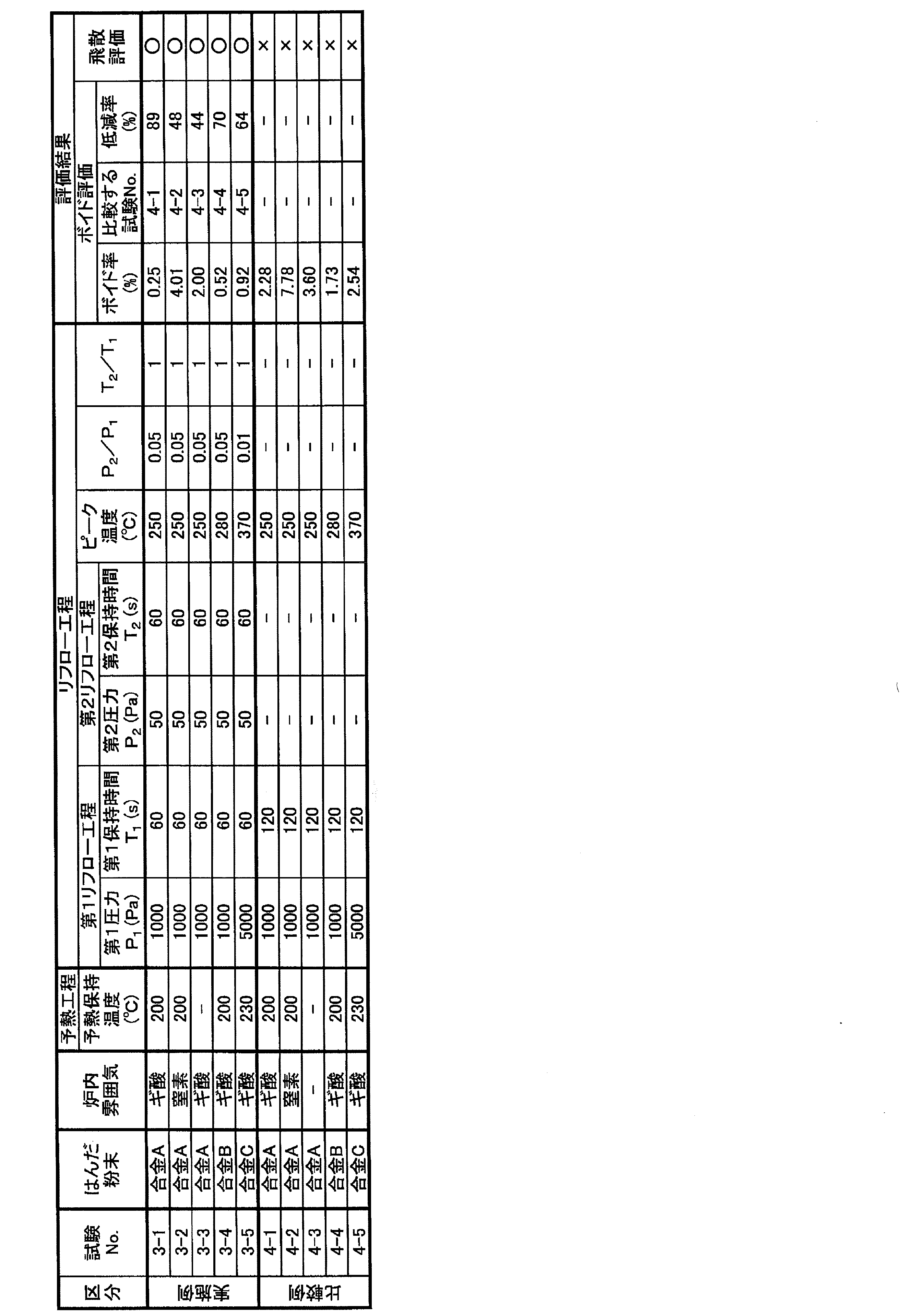
表2の結果から分かるように、本発明の構成要件をすべて満たす試験No.3-1~3-5の試験基板は、第2リフロー工程を行わない試験No.4-1~4-5の試験基板と比較して、接合部におけるボイドを低減し、かつ、はんだ材料の飛散を抑制することができる。
[試験3]
<試験基板の作製>
(試験No.5)
まず、合金A(96.5Sn/3.0Ag/0.5Cu)粉末とフラックスとを混合して、ソルダペーストを作製した。前記フラックスは、ペーストフラックス(弘輝社製、製品名:ペーストフラックス(RMAタイプ))を用いた。次に、ガラスエポキシ基板(サイズ:50×50mm、厚み:1.6mm)を準備した。前記基板上には銅箔にてφ0.2mmのパターンを形成し、プリフラックス(商品名「タフエース」、四国化成社製)で処理した。前記基板に前記ソルダペーストを、厚さ150μmのメタルマスクを用いて開口率400%となるように塗布し、リフロー装置(商品名:VS1、オリジン電気社製)のリフロー炉内に配置した。塗布したソルダペーストの厚さは150μmであった。そして、後述する予熱工程及びリフロー工程を行うことにより、試験No.5の試験基板を作製した。
予熱工程では、まず、窒素雰囲気下において、昇温速度1.7℃/sで予熱温度200℃まで加熱した。そして、該予熱温度において、真空ポンプを用いてリフロー炉内の気体を排気して30s保持した後、ギ酸(3%)を導入することによりリフロー炉内の雰囲気を大気圧まで加圧して240s保持した。
続いて、リフロー工程では、まず、リフロー炉内の雰囲気を5000Pa(第1圧力P1)へ減圧した後、昇温速度2.6℃/sでピーク温度250℃まで加熱し、60s(第1保持時間T1)保持した(第1リフロー工程)。次に、リフロー炉内の雰囲気を100Pa(第2圧力P2)まで減圧した後、60s(第2保持時間T2)保持した(第2リフロー工程)。最後に、ピーク温度250℃にて、リフロー炉内に窒素を導入することにより大気圧まで加圧した。前記第1リフロー工程及び前記第2リフロー工程の条件を表3に示す。
(試験No.6)
第2リフロー工程を行わなかったこと以外は、試験No.5と同様に試験No.6の試験基板を作製した。リフロー工程の詳細な条件を表3に示す。
第2リフロー工程を行わなかったこと以外は、試験No.5と同様に試験No.6の試験基板を作製した。リフロー工程の詳細な条件を表3に示す。
<ボイド評価>
試験1と同様の方法で、ボイドの評価を行った。結果を表3に示す。
試験1と同様の方法で、ボイドの評価を行った。結果を表3に示す。
<飛散評価>
試験1と同様の方法で、ボイドの評価を行った。結果を表3に示す。
試験1と同様の方法で、ボイドの評価を行った。結果を表3に示す。

表3の結果から分かるように、本発明の構成要件をすべて満たす試験No.5の試験基板は、第2リフロー工程を行わない試験No.6の試験基板と比較して、接合部におけるボイドを低減し、かつ、はんだ材料の飛散を抑制することができる。
Claims (5)
- リフロー炉内で、はんだ材料と第1部材とを接触させた状態で加熱し、前記はんだ材料を構成するはんだ合金を溶融させるリフロー工程を備え、
前記リフロー工程は、
前記リフロー炉内の雰囲気を大気圧よりも低い第1圧力P1まで減圧した状態で前記はんだ合金を溶融させる第1リフロー工程と、
前記第1リフロー工程後、前記リフロー炉内の雰囲気を前記第1圧力P1よりも低い第2圧力P2まで減圧した状態で前記はんだ合金を溶融させる第2リフロー工程と、
を含む、接合構造体の製造方法。 - 前記リフロー工程は、リフロー炉内で、はんだ材料を介して第1部材と第2部材とを接触させた状態で加熱し、前記はんだ材料を構成するはんだ合金を溶融させる、請求項1に記載の接合構造体の製造方法。
- 前記第1圧力P1に対する前記第2圧力P2の比(P2/P1)は、0.0017~0.8である、請求項1又は2に記載の接合構造体の製造方法。
- 前記第1リフロー工程では、ピーク温度で第1保持時間T1保持し、
前記第2リフロー工程では、ピーク温度で第2保持時間T2保持し、
前記第1保持時間T1に対する前記第2保持時間T2の比(T2/T1)は、0.017~59である、請求項1~3のいずれか一つに記載の接合構造体の製造方法。 - 前記リフロー工程は、さらに、前記第2リフロー工程後、前記はんだ合金の融点以上の温度で、前記リフロー炉内の雰囲気を大気圧まで加圧する第3リフロー工程を含む、請求項1~4のいずれか一つに記載の接合構造体の製造方法。
Priority Applications (4)
| Application Number | Priority Date | Filing Date | Title |
|---|---|---|---|
| EP19869346.7A EP3838465B1 (en) | 2018-10-01 | 2019-10-01 | Method for producing bonded structure |
| KR1020217005009A KR102259122B1 (ko) | 2018-10-01 | 2019-10-01 | 접합 구조체의 제조 방법 |
| US17/276,990 US11446752B2 (en) | 2018-10-01 | 2019-10-01 | Method for producing joined structure |
| CN201980058479.5A CN112654453B (zh) | 2018-10-01 | 2019-10-01 | 接合结构体的制造方法 |
Applications Claiming Priority (2)
| Application Number | Priority Date | Filing Date | Title |
|---|---|---|---|
| JP2018-186574 | 2018-10-01 | ||
| JP2018186574A JP6709944B2 (ja) | 2018-10-01 | 2018-10-01 | 接合構造体の製造方法 |
Publications (1)
| Publication Number | Publication Date |
|---|---|
| WO2020071357A1 true WO2020071357A1 (ja) | 2020-04-09 |
Family
ID=70055169
Family Applications (1)
| Application Number | Title | Priority Date | Filing Date |
|---|---|---|---|
| PCT/JP2019/038727 WO2020071357A1 (ja) | 2018-10-01 | 2019-10-01 | 接合構造体の製造方法 |
Country Status (7)
| Country | Link |
|---|---|
| US (1) | US11446752B2 (ja) |
| EP (1) | EP3838465B1 (ja) |
| JP (1) | JP6709944B2 (ja) |
| KR (1) | KR102259122B1 (ja) |
| CN (1) | CN112654453B (ja) |
| TW (1) | TWI825188B (ja) |
| WO (1) | WO2020071357A1 (ja) |
Citations (5)
| Publication number | Priority date | Publication date | Assignee | Title |
|---|---|---|---|---|
| JP2005205418A (ja) * | 2004-01-20 | 2005-08-04 | Denso Corp | 接合構造体の製造方法 |
| JP2010000513A (ja) * | 2008-06-18 | 2010-01-07 | Sharp Corp | 接合構造体の製造方法 |
| JP2012129482A (ja) * | 2010-12-17 | 2012-07-05 | Toshiba Corp | 半導体装置の製造方法 |
| JP2016155141A (ja) * | 2015-02-24 | 2016-09-01 | 株式会社タムラ製作所 | はんだ接合構造体の製造方法 |
| WO2017057651A1 (ja) | 2015-09-30 | 2017-04-06 | オリジン電気株式会社 | 還元ガス用ソルダペースト、半田付け製品の製造方法 |
Family Cites Families (15)
| Publication number | Priority date | Publication date | Assignee | Title |
|---|---|---|---|---|
| US5440101A (en) * | 1993-04-19 | 1995-08-08 | Research, Incorporated | Continuous oven with a plurality of heating zones |
| JP3649950B2 (ja) * | 1999-06-14 | 2005-05-18 | 株式会社日立製作所 | 冷却部品取付方法 |
| JP2001058259A (ja) * | 1999-06-18 | 2001-03-06 | Shinko Seiki Co Ltd | 半田付け方法及び半田付け装置 |
| JP2001077524A (ja) * | 1999-09-03 | 2001-03-23 | Fujitsu Ltd | リフロー半田付け装置及びリフロー半田付け方法 |
| JP4404000B2 (ja) * | 2005-04-05 | 2010-01-27 | トヨタ自動車株式会社 | 接合構造体の製造方法 |
| JP4956963B2 (ja) * | 2005-11-02 | 2012-06-20 | 富士通セミコンダクター株式会社 | リフロー装置、リフロー方法、および半導体装置の製造方法 |
| JP2007180447A (ja) | 2005-12-28 | 2007-07-12 | Toyota Industries Corp | 半田付け方法、半田付け装置、及び半導体装置の製造方法 |
| DE102007005345B4 (de) * | 2007-02-02 | 2014-06-18 | Seho Systemtechnik Gmbh | Verfahren zum Reflow-Löten sowie Vorrichtung zur Durchführung des Verfahrens |
| JP5378078B2 (ja) * | 2009-06-19 | 2013-12-25 | 株式会社東芝 | 半導体装置の製造方法 |
| US8061578B2 (en) * | 2010-02-03 | 2011-11-22 | Indium Corporation | Solder preform |
| JP5540916B2 (ja) * | 2010-06-15 | 2014-07-02 | デクセリアルズ株式会社 | 接続構造体の製造方法 |
| WO2012070264A1 (ja) | 2010-11-23 | 2012-05-31 | 三菱電機株式会社 | リフローはんだ付け装置およびリフローはんだ付け方法 |
| JP5835533B2 (ja) * | 2013-07-23 | 2015-12-24 | 千住金属工業株式会社 | はんだ付け装置及び真空はんだ付け方法 |
| MY176643A (en) * | 2016-11-22 | 2020-08-19 | Senju Metal Industry Co | Soldering method |
| CN107222982B (zh) | 2017-05-25 | 2019-09-03 | 杭州晶志康电子科技有限公司 | 一种smt贴片工艺 |
-
2018
- 2018-10-01 JP JP2018186574A patent/JP6709944B2/ja active Active
-
2019
- 2019-10-01 WO PCT/JP2019/038727 patent/WO2020071357A1/ja unknown
- 2019-10-01 KR KR1020217005009A patent/KR102259122B1/ko active IP Right Grant
- 2019-10-01 TW TW108135550A patent/TWI825188B/zh active
- 2019-10-01 CN CN201980058479.5A patent/CN112654453B/zh active Active
- 2019-10-01 EP EP19869346.7A patent/EP3838465B1/en active Active
- 2019-10-01 US US17/276,990 patent/US11446752B2/en active Active
Patent Citations (5)
| Publication number | Priority date | Publication date | Assignee | Title |
|---|---|---|---|---|
| JP2005205418A (ja) * | 2004-01-20 | 2005-08-04 | Denso Corp | 接合構造体の製造方法 |
| JP2010000513A (ja) * | 2008-06-18 | 2010-01-07 | Sharp Corp | 接合構造体の製造方法 |
| JP2012129482A (ja) * | 2010-12-17 | 2012-07-05 | Toshiba Corp | 半導体装置の製造方法 |
| JP2016155141A (ja) * | 2015-02-24 | 2016-09-01 | 株式会社タムラ製作所 | はんだ接合構造体の製造方法 |
| WO2017057651A1 (ja) | 2015-09-30 | 2017-04-06 | オリジン電気株式会社 | 還元ガス用ソルダペースト、半田付け製品の製造方法 |
Non-Patent Citations (1)
| Title |
|---|
| See also references of EP3838465A4 |
Also Published As
| Publication number | Publication date |
|---|---|
| EP3838465B1 (en) | 2024-01-17 |
| JP2020055011A (ja) | 2020-04-09 |
| CN112654453A (zh) | 2021-04-13 |
| US20210260679A1 (en) | 2021-08-26 |
| EP3838465A4 (en) | 2021-12-01 |
| EP3838465A1 (en) | 2021-06-23 |
| US11446752B2 (en) | 2022-09-20 |
| CN112654453B (zh) | 2023-03-24 |
| JP6709944B2 (ja) | 2020-06-17 |
| EP3838465C0 (en) | 2024-01-17 |
| TWI825188B (zh) | 2023-12-11 |
| KR20210029820A (ko) | 2021-03-16 |
| KR102259122B1 (ko) | 2021-06-01 |
| TW202021717A (zh) | 2020-06-16 |
Similar Documents
| Publication | Publication Date | Title |
|---|---|---|
| CN109923951B (zh) | 软钎焊方法 | |
| JPH06297185A (ja) | 動的ハンダペースト組成物 | |
| JPWO2011027820A1 (ja) | 鉛フリーはんだ合金、接合用部材及びその製造法、並びに電子部品 | |
| JP2018511482A5 (ja) | ||
| JP5031677B2 (ja) | 接合構造体の製造方法 | |
| WO2015178374A1 (ja) | はんだバンプの形成方法及びはんだボール固定用はんだペースト | |
| JP3400408B2 (ja) | フリップチップ実装方法 | |
| TW201615314A (zh) | 焊料膏 | |
| JP2001274539A (ja) | 電子デバイス搭載プリント配線板の電極接合方法 | |
| WO2020071357A1 (ja) | 接合構造体の製造方法 | |
| JP4008799B2 (ja) | 無鉛はんだペースト組成物およびはんだ付け方法 | |
| JP4747281B2 (ja) | Au−Sn合金はんだペーストを用いた基板と素子の接合方法 | |
| JP6089243B2 (ja) | 接合構造体の製造方法 | |
| KR102122166B1 (ko) | 솔더 페이스트용 플럭스, 솔더 페이스트, 솔더 페이스트를 사용한 솔더 범프의 형성 방법 및 접합체의 제조 방법 | |
| JP5391584B2 (ja) | ボイド発生の少ないAu−Sn合金はんだペーストを用いた基板と素子の接合方法 | |
| JP2016157766A (ja) | はんだバンプのリフロー方法 | |
| JP2017087248A (ja) | はんだペースト組成物 | |
| JP2004001030A (ja) | はんだペーストおよび半導体装置の製造方法 | |
| JP2000052027A (ja) | 耐高温用金属接合法 | |
| JP2016140870A (ja) | はんだバンプの形成方法 | |
| JPWO2019117041A1 (ja) | ソルダペースト、接合構造体及び接合構造体の製造方法 | |
| JPH05259632A (ja) | プリント配線板およびその製造方法 | |
| JP2004311679A (ja) | はんだ付け方法とそのプリント配線板 | |
| JP2022129960A (ja) | フラックス、ソルダペースト、及び、接合構造体の製造方法 | |
| JP2004022849A (ja) | フレキシブルプリント配線基板並びに無鉛半田付け方法 |
Legal Events
| Date | Code | Title | Description |
|---|---|---|---|
| 121 | Ep: the epo has been informed by wipo that ep was designated in this application |
Ref document number: 19869346 Country of ref document: EP Kind code of ref document: A1 |
|
| ENP | Entry into the national phase |
Ref document number: 20217005009 Country of ref document: KR Kind code of ref document: A |
|
| ENP | Entry into the national phase |
Ref document number: 2019869346 Country of ref document: EP Effective date: 20210316 |
|
| NENP | Non-entry into the national phase |
Ref country code: DE |