WO2020071022A1 - 樹脂フィルムおよびその製造方法 - Google Patents
樹脂フィルムおよびその製造方法Info
- Publication number
- WO2020071022A1 WO2020071022A1 PCT/JP2019/034084 JP2019034084W WO2020071022A1 WO 2020071022 A1 WO2020071022 A1 WO 2020071022A1 JP 2019034084 W JP2019034084 W JP 2019034084W WO 2020071022 A1 WO2020071022 A1 WO 2020071022A1
- Authority
- WO
- WIPO (PCT)
- Prior art keywords
- resin film
- conductive
- resin
- compound
- weight
- Prior art date
- Legal status (The legal status is an assumption and is not a legal conclusion. Google has not performed a legal analysis and makes no representation as to the accuracy of the status listed.)
- Ceased
Links
Images

Classifications
-
- C—CHEMISTRY; METALLURGY
- C08—ORGANIC MACROMOLECULAR COMPOUNDS; THEIR PREPARATION OR CHEMICAL WORKING-UP; COMPOSITIONS BASED THEREON
- C08J—WORKING-UP; GENERAL PROCESSES OF COMPOUNDING; AFTER-TREATMENT NOT COVERED BY SUBCLASSES C08B, C08C, C08F, C08G or C08H
- C08J7/00—Chemical treatment or coating of shaped articles made of macromolecular substances
- C08J7/04—Coating
- C08J7/044—Forming conductive coatings; Forming coatings having anti-static properties
-
- B—PERFORMING OPERATIONS; TRANSPORTING
- B32—LAYERED PRODUCTS
- B32B—LAYERED PRODUCTS, i.e. PRODUCTS BUILT-UP OF STRATA OF FLAT OR NON-FLAT, e.g. CELLULAR OR HONEYCOMB, FORM
- B32B3/00—Layered products comprising a layer with external or internal discontinuities or unevennesses, or a layer of non-planar shape; Layered products comprising a layer having particular features of form
- B32B3/10—Layered products comprising a layer with external or internal discontinuities or unevennesses, or a layer of non-planar shape; Layered products comprising a layer having particular features of form characterised by a discontinuous layer, i.e. formed of separate pieces of material
- B32B3/14—Layered products comprising a layer with external or internal discontinuities or unevennesses, or a layer of non-planar shape; Layered products comprising a layer having particular features of form characterised by a discontinuous layer, i.e. formed of separate pieces of material characterised by a face layer formed of separate pieces of material which are juxtaposed side-by-side
-
- B—PERFORMING OPERATIONS; TRANSPORTING
- B32—LAYERED PRODUCTS
- B32B—LAYERED PRODUCTS, i.e. PRODUCTS BUILT-UP OF STRATA OF FLAT OR NON-FLAT, e.g. CELLULAR OR HONEYCOMB, FORM
- B32B7/00—Layered products characterised by the relation between layers; Layered products characterised by the relative orientation of features between layers, or by the relative values of a measurable parameter between layers, i.e. products comprising layers having different physical, chemical or physicochemical properties; Layered products characterised by the interconnection of layers
- B32B7/02—Physical, chemical or physicochemical properties
- B32B7/025—Electric or magnetic properties
-
- C—CHEMISTRY; METALLURGY
- C08—ORGANIC MACROMOLECULAR COMPOUNDS; THEIR PREPARATION OR CHEMICAL WORKING-UP; COMPOSITIONS BASED THEREON
- C08J—WORKING-UP; GENERAL PROCESSES OF COMPOUNDING; AFTER-TREATMENT NOT COVERED BY SUBCLASSES C08B, C08C, C08F, C08G or C08H
- C08J5/00—Manufacture of articles or shaped materials containing macromolecular substances
- C08J5/18—Manufacture of films or sheets
-
- C—CHEMISTRY; METALLURGY
- C08—ORGANIC MACROMOLECULAR COMPOUNDS; THEIR PREPARATION OR CHEMICAL WORKING-UP; COMPOSITIONS BASED THEREON
- C08J—WORKING-UP; GENERAL PROCESSES OF COMPOUNDING; AFTER-TREATMENT NOT COVERED BY SUBCLASSES C08B, C08C, C08F, C08G or C08H
- C08J7/00—Chemical treatment or coating of shaped articles made of macromolecular substances
- C08J7/04—Coating
-
- C—CHEMISTRY; METALLURGY
- C08—ORGANIC MACROMOLECULAR COMPOUNDS; THEIR PREPARATION OR CHEMICAL WORKING-UP; COMPOSITIONS BASED THEREON
- C08J—WORKING-UP; GENERAL PROCESSES OF COMPOUNDING; AFTER-TREATMENT NOT COVERED BY SUBCLASSES C08B, C08C, C08F, C08G or C08H
- C08J7/00—Chemical treatment or coating of shaped articles made of macromolecular substances
- C08J7/04—Coating
- C08J7/042—Coating with two or more layers, where at least one layer of a composition contains a polymer binder
-
- C—CHEMISTRY; METALLURGY
- C08—ORGANIC MACROMOLECULAR COMPOUNDS; THEIR PREPARATION OR CHEMICAL WORKING-UP; COMPOSITIONS BASED THEREON
- C08K—Use of inorganic or non-macromolecular organic substances as compounding ingredients
- C08K3/00—Use of inorganic substances as compounding ingredients
- C08K3/18—Oxygen-containing compounds, e.g. metal carbonyls
- C08K3/20—Oxides; Hydroxides
- C08K3/22—Oxides; Hydroxides of metals
-
- C—CHEMISTRY; METALLURGY
- C09—DYES; PAINTS; POLISHES; NATURAL RESINS; ADHESIVES; COMPOSITIONS NOT OTHERWISE PROVIDED FOR; APPLICATIONS OF MATERIALS NOT OTHERWISE PROVIDED FOR
- C09D—COATING COMPOSITIONS, e.g. PAINTS, VARNISHES OR LACQUERS; FILLING PASTES; CHEMICAL PAINT OR INK REMOVERS; INKS; CORRECTING FLUIDS; WOODSTAINS; PASTES OR SOLIDS FOR COLOURING OR PRINTING; USE OF MATERIALS THEREFOR
- C09D5/00—Coating compositions, e.g. paints, varnishes or lacquers, characterised by their physical nature or the effects produced; Filling pastes
- C09D5/24—Electrically-conducting paints
-
- C—CHEMISTRY; METALLURGY
- C09—DYES; PAINTS; POLISHES; NATURAL RESINS; ADHESIVES; COMPOSITIONS NOT OTHERWISE PROVIDED FOR; APPLICATIONS OF MATERIALS NOT OTHERWISE PROVIDED FOR
- C09D—COATING COMPOSITIONS, e.g. PAINTS, VARNISHES OR LACQUERS; FILLING PASTES; CHEMICAL PAINT OR INK REMOVERS; INKS; CORRECTING FLUIDS; WOODSTAINS; PASTES OR SOLIDS FOR COLOURING OR PRINTING; USE OF MATERIALS THEREFOR
- C09D7/00—Features of coating compositions, not provided for in group C09D5/00; Processes for incorporating ingredients in coating compositions
- C09D7/40—Additives
- C09D7/60—Additives non-macromolecular
- C09D7/61—Additives non-macromolecular inorganic
-
- C—CHEMISTRY; METALLURGY
- C08—ORGANIC MACROMOLECULAR COMPOUNDS; THEIR PREPARATION OR CHEMICAL WORKING-UP; COMPOSITIONS BASED THEREON
- C08J—WORKING-UP; GENERAL PROCESSES OF COMPOUNDING; AFTER-TREATMENT NOT COVERED BY SUBCLASSES C08B, C08C, C08F, C08G or C08H
- C08J2367/00—Characterised by the use of polyesters obtained by reactions forming a carboxylic ester link in the main chain; Derivatives of such polymers
Definitions
- the present invention relates to a resin film and a method for producing the same.
- Thermoplastic resin films especially biaxially oriented polyester films, have excellent properties such as mechanical properties, electrical properties, dimensional stability, transparency, and chemical resistance. Widely used in applications.
- various optics including display members such as touch panels, liquid crystal display panels (LCD), plasma display panels (PDP), and organic electroluminescence (organic EL).
- display members such as touch panels, liquid crystal display panels (LCD), plasma display panels (PDP), and organic electroluminescence (organic EL).
- LCD liquid crystal display panels
- PDP plasma display panels
- organic EL organic electroluminescence
- Patent Literature 1 describes a method of applying antistatic to a polyester resin and coating the same
- Patent Literature 2 describes a method of coating a styrene sulfonic acid copolymer.
- the antistatic property fluctuates due to environmental changes such as humidity and temperature during use, and elapsed time from manufacture.
- scratch resistance is provided for the purpose of suppressing surface scraping due to contact or slippage on the transport roll during processing.
- a hard coat film formed by laminating a layer (hard coat layer) made of an ultraviolet (UV) curable resin is used.
- UV ultraviolet
- a scratch-resistant layer is not cracked. Workability that neatly punches through is required. If the workability is poor, cracks will occur at the ends, impairing the design properties, or the fragments will lead to defects.
- Patent Document 3 proposes a film in which a conductive material is mixed in a hard coat layer
- Patent Document 4 proposes a laminated film in which the upper surface of an antistatic layer is further coated with a hard coat layer.
- Patent Literature 3 fails to sufficiently satisfy both the scratch resistance and the antistatic property. Further, in the technique of Patent Document 4, the antistatic performance becomes insufficient in the step after the hard coat processing.
- an object of the present invention is to provide a technique capable of solving the above-mentioned disadvantages and stably mass-producing a resin film capable of achieving both antistatic properties and scratch resistance.
- the resin film of the present invention has the following configuration.
- At least one surface has an insulating phase (A) and a conductive phase (B) measured by a conductivity measurement mode (conductive AFM) of AFM (Atomic Force Microscope (atomic force microscope)).
- conductive AFM conductivity measurement mode
- AFM Atomic Force Microscope
- the insulating phase (A) of the conductive I A and the conductive phase (B) of the conductive I B ratio I A / I B is 100 or more in the surface alpha, is 100,000 (1) or ( The resin film according to 2).
- the resin film according to 2). (4) The resin film according to any one of (1) to (3), wherein a change in haze on the surface ⁇ before and after the rubbing treatment is 3.0% or less.
- the resin film according to any one of (1) to (4), wherein the elastic modulus (G A ) of the insulating phase (A) on the surface ⁇ is from 2000 MPa to 50,000 MPa.
- the resin film according to any one of (1) to (5) is a laminate of two or more layers including a support substrate and a layer (X) having a surface formed thereon.
- the insulating phase (A) contains metal oxide particles (a) containing at least one metal element selected from the group consisting of Si, Al, Ti, Zr, Se and Fe.
- the resin film of the present invention has both antistatic properties and scratch resistance, has little change in antistatic properties depending on the environment (ie, has excellent stability), and reduces the number of steps in the manufacturing process to reduce the manufacturing load. You can do it.
- FIG. 2 is a schematic diagram showing a distribution of conductivity obtained by conducting a conductivity measurement mode (conductive AFM) measurement of the surface of the resin film of the present invention by AFM (Atomic Force Microscope).
- conductive AFM conductivity measurement mode
- AFM Anamic Force Microscope
- the resin film of the present invention has at least one surface having an insulating phase (A) and a conductive phase (B) measured by a conductive measurement mode (conductive AFM) of AFM (Atomic Force Microscope).
- conductive AFM conductive measurement mode of AFM
- FIG. 1 shows a schematic diagram of the distribution of conductivity measured on the surface of the resin film of the present invention by conductive AFM.
- the resin film of the present invention needs to have two domains having different physical properties on at least one surface. Specifically, when the surface is measured by the conductive AFM method, a domain having a relatively high conductivity (hereinafter referred to as a conductive phase (B)) and a domain having a relatively low conductivity (hereinafter referred to as an insulating phase (A)) Must be present).
- a conductive phase (B) a domain having a relatively high conductivity
- A insulating phase
- the image obtained by the conductive AFM measurement is binarized by “ScionImage” (maximum value: 10 nA, minimum value: 0 pA, threshold value 180 (black is set to 0, white is set to 255, and black to white is set to In the gray scale represented by 256 levels, a conductive image is created by setting the area where 10 nA or more flows to 255 (white) and the area of 0 pA to 0 (black), and a gray scale 180 is obtained in the obtained conductive image. A portion where the current value represented by the above color tone is high is colored white, and a portion where the current value represented by a color tone less than 180 is low is colored black)) to obtain a conductive image.
- the obtained conductive image of 1 ⁇ m ⁇ 1 ⁇ m is vertically and horizontally divided into 40 regions, and divided into 1600 regions of 25 nm ⁇ 25 nm.
- a white color is referred to as a conductive phase (B).
- the present inventors have studied, the material used to impart antistatic properties, is often configured as a set of low hardness polymer or low molecular weight material, It has been confirmed that its characteristics are easily changed by external stimuli such as pressure, temperature and humidity.
- an insulating phase (A) which is a domain substantially free of an antistatic component, on the film surface, the antistatic property and the scratch resistance are compatible, and the antistatic property is stabilized. I found what I could achieve.
- the area occupied by the insulating phase (A) needs to be 40% or more and 80% or less. If the area occupied by the entire surface ⁇ is less than 40%, the antistatic performance may be unstable, or the scratch resistance may be insufficient, which is not practical. On the other hand, if the area occupying the entire surface ⁇ exceeds 80%, the antistatic performance is insufficient, which is not preferable.
- control of the compatibility of the resin material and adjustment of the coating and drying conditions, and when using a filler material, the amount of the filler material and the particle diameter are used. Can be adjusted. A specific method for measuring each region, a preferable coating composition, and a manufacturing method will be described later. A particularly preferred range of the area occupying the entire surface ⁇ of the insulating phase (A) is from 40% to 60%.
- the haze change before and after rubbing the surface ⁇ of the resin film of the present invention will be described.
- the haze indicates a value defined by JIS K7136 (2000)
- the haze of the film is mainly treated as an index indicating the transparency of the film.
- the transparency is reduced. Therefore, comparing the haze values before and after the rubbing treatment is equivalent to evaluating the amount of surface flaws caused by the rubbing treatment.
- the surface ⁇ of the resin film of the present invention preferably has a haze change of 3.0% or less before and after rubbing under the conditions described below.
- a haze change of 3.0% or less before and after rubbing under the conditions described below.
- it exceeds 3.0% it means that the hardness of the coating film is insufficient, or sufficient film-forming properties are not obtained, or the formation of the insulating phase (A) described below is insufficient.
- the specific method of the rubbing treatment and the method of measuring the haze will be described later. It is more preferably at most 2.5%, further preferably at most 1.9%.
- the surface ⁇ of the resin film of the present invention needs to have a surface resistivity of 1 ⁇ 10 10 ⁇ / ⁇ or less.
- the surface resistivity is a value obtained by a measurement method described later, and is an index indicating the average conductivity of the resin film surface in a macroscopic range as compared with the measurement in the conductivity measurement mode of the AFM. If the surface resistivity exceeds 1 ⁇ 10 10 ⁇ / ⁇ , the above-mentioned ratio of the insulating phase (A) is too large or the performance of the conductive phase (B) is insufficient. Performance cannot be obtained.
- the method for measuring the surface resistivity will be described later.
- the surface resistivity is preferably 1 ⁇ 10 9 ⁇ / ⁇ or less, particularly preferably 1 ⁇ 10 7 ⁇ / ⁇ or less.
- the lower limit is not particularly limited, but is preferably 1 ⁇ 10 4 ⁇ / ⁇ or more in a practical configuration from the viewpoint of film forming property and cost.
- the resin constituting the resin film in the present invention is not particularly limited, and examples thereof include known acrylic resins, polyester resins, urethane resins, melamine resins, and epoxy resins.
- an acrylic resin and a melamine resin are preferred from the viewpoint of stability in the case of being produced by a preferred production method described later.
- the resin film in the present invention may be any one having a surface ⁇ satisfying the above-mentioned conditions on at least one surface, and may be a single-layer film or a laminated film. It may have a layer formed on at least one surface or both surfaces of the support substrate.
- the “layer” in the present invention refers to a boundary from the surface of the laminate to the thickness direction, where the composition of constituent elements, the shape of inclusions such as particles, and the physical properties in the thickness direction are discontinuous with adjacent parts.
- the laminated body is subjected to various composition / elemental analysis apparatuses (FT-IR, XPS, XRF, EDAX, SIMS, EPMA, EELS, etc.) in the thickness direction from the surface, an electron microscope (transmission type, scanning type) or When a cross section is observed with an optical microscope, it refers to a portion that is distinguished by the discontinuous boundary surface and has a finite thickness.
- composition / elemental analysis apparatuses FT-IR, XPS, XRF, EDAX, SIMS, EPMA, EELS, etc.
- the resin film of the present invention preferably has a layer (X) on at least one surface of the support substrate, which is designed from the viewpoint of antistatic properties and scratch resistance, and the layer (X) has the surface. It is preferable to have ⁇ .
- the resin constituting the layer (X) the resins listed above as the resin constituting the resin film can be preferably used.
- the method for forming the layer (X) is not particularly limited as long as the above-mentioned conditions can be satisfied, but it is preferable that the layer (X) is formed from a coating composition.
- a film to which a coating composition described later is applied may be prepared in the course of forming the supporting base material, or after forming the supporting base material, the coating composition is applied to the supporting base material, and dried and wound. You may.
- the thickness of the layer (X) is preferably 10 to 2000 nm, more preferably 40 to 1000 nm, and further preferably 80 to 800 nm.
- the thickness is from 10 nm to 2000 nm, the functions desired to be imparted by the layer (X), that is, antistatic properties, scratch resistance and coating film quality can be obtained, which is preferable.
- the conductive phase (B) and the insulating phase (A) are observed on at least one surface when measured by the conductive AFM.
- Atomic force microscope is a method of measuring the uneven shape by scanning the surface shape using a cantilever having a sharp tip at the atomic level.In this measurement, a cantilever having conductivity is used, and the cantilever is used. -By applying a voltage between samples, it is possible to detect and map the generation of a weak current on the film surface. Such a measurement is referred to as a conductivity measurement mode or a conductive AFM (c-AFM).
- Conductive AFM measurement can detect a minute current (tunnel current) that seeps out of the insulating air layer, and a slight difference in conductivity in a minute area directly below the cantilever (the conductivity of the film surface). ) Can be detected efficiently. Details and a measuring method will be described later.
- the average domain diameter of the insulating phase (A) on the surface ⁇ is preferably from 50 nm to 200 nm, particularly preferably from 50 nm to 100 nm. If the average domain diameter of the insulating phase (A) is less than 50 nm, the scratch resistance may be reduced and the antistatic performance may be unstable. On the other hand, when the average domain diameter of the insulating phase (A) exceeds 200 nm, formation of a conductive path is hindered, and as a result, sufficient antistatic properties may not be obtained.
- the control can be performed using the particle diameter.
- Conductive I A conductive I B and the insulating phase of the conductive phase (B) (A)] There is a preferable numerical range for the current value (conductivity index) obtained when the resin film of the present invention is measured by the conductive AFM.
- Conductive phase Specifically (B) of the conductive I B and the insulating phase (A) the ratio I B / I A conductive I B is 100 or more, preferably 100,000 or less, 3000 100,000 Particularly preferred.
- the conductivity ratio I B / I A is less than 100, the formation of the above-described separated structure of the insulating phase (A) and the conductive phase (B) becomes insufficient, and the case where the scratch resistance is insufficient or the electrification occurs. Prevention performance may be unstable.
- the upper limit is not particularly limited, but is preferably 100,000 or less. Details and a measuring method will be described later.
- the surface ⁇ of the resin film of the present invention has a preferable numerical range for the elastic modulus measured by an atomic force microscope.
- modulus G A is 50000MPa is preferably from more than 2000MPa insulating phase (A), and particularly preferably more than 5000 MPa 20000 MPa.
- A 2000MPa insulating phase
- the above-mentioned scratch resistance may not be obtained, or the stability of antistatic performance may not be obtained.
- it exceeds 50,000 MPa the workability of the film may be reduced, for example, cracks may easily occur when the film is processed.
- the surface ⁇ of the resin film of the present invention there is a preferred range in the ratio G A / G B modulus G B of the elastic modulus G A and the electrically conductive phase (B) of the insulating phase (A).
- the G A / G B is 4 or more and 20 or less, more preferably 6 to 16, particularly preferably 8 to 12.
- G A / G B is less than 4 or more than 20, the hardness of the resin film is biased toward the flexible side or the hard side, so that it may be difficult to achieve both scratch resistance and workability.
- the elastic modulus G B of the conductive phase (B) is preferably not more than 2000MPa or more 500 MPa. If it is less than 500 MPa, the scratch resistance of the resin film may decrease, and if it exceeds 2000 MPa, the workability may decrease.
- the elastic modulus measurement by the atomic force microscope is a compression test using a probe of an extremely small part, and is a degree of deformation due to a pressing force.
- the elastic modulus of the surface ⁇ and its elasticity are measured.
- the spatial distribution can be measured. Specifically, by obtaining a force curve, which will be described later, in each region detected as the conductive phase (B) or the insulating phase (A) in the above-described conductivity measurement, elastic modulus information of each region is obtained. Becomes possible.
- the probe at the tip of the cantilever is brought into contact with the surface ⁇ , and the deflection of the cantilever obtained by measuring the force curve with a pressing force of 55 nN. The amount can be measured.
- the spatial resolution depends on the scanning range and the number of scanning lines of the atomic force microscope, but under practical measurement conditions, the lower limit is about 50 nm. Details and a measuring method will be described later.
- the resin film of the present invention may be a single-layer film or a laminated film, but is preferably in the form of a support base material and a layer having a surface ⁇ on at least one surface thereof (X ) Is a laminated resin film.
- the resin used as the supporting substrate is not particularly limited, but polyester is mentioned from the viewpoint of heat resistance and cost.
- the support base material is preferably a layer mainly composed of polyester (hereinafter, a layer mainly composed of polyester used as a support base material may be called a polyester film).
- the main component refers to a component that accounts for 50% by weight or more of the entire resin constituting the layer.
- the content of the particles in the support substrate is preferably 0.1% by weight or less based on the entire support substrate.
- the internal haze can be reduced to 0.2% or less, and a resin film having excellent transparency can be obtained.
- polyester is a generic term for polymers having an ester bond in the main chain, and includes ethylene terephthalate, propylene terephthalate, ethylene-2,6-naphthalate, butylene terephthalate, propylene-2,6-naphthalate, ethylene- ⁇ , ⁇
- Those containing at least one component selected from -bis (2-chlorophenoxy) ethane-4,4'-dicarboxylate and the like can be preferably used.
- the polyester film using the above polyester is preferably biaxially oriented.
- a biaxially oriented polyester film is generally formed by stretching a polyester sheet or film in an unstretched state about 2.5 to 5 times in a longitudinal direction and a width direction orthogonal to the longitudinal direction, and then performing a heat treatment to obtain a crystal. This means that the orientation has been completed and shows a biaxial orientation pattern in wide-angle X-ray diffraction.
- thermal stability, especially dimensional stability and mechanical strength are sufficient, and flatness is also good.
- additives for example, antioxidants, heat stabilizers, weather stabilizers, ultraviolet absorbers, organic lubricants, pigments, dyes, organic or inorganic fine particles, fillers, antistatic An agent, a nucleating agent and the like may be added to such an extent that the characteristics are not deteriorated.
- the thickness of the polyester film is not particularly limited and is appropriately selected depending on the application and type. However, from the viewpoint of mechanical strength, handling properties, and the like, it is usually preferably from 10 to 500 ⁇ m, more preferably from 15 to 250 ⁇ m. , Most preferably from 20 to 200 ⁇ m. Further, the polyester film may be a composite film obtained by co-extrusion or a film obtained by laminating the obtained films by various methods.
- the resin film of the present invention is obtained by applying a coating composition containing metal oxide particles (a) and a binder component onto a polyester film, and drying the solvent when the coating composition contains a solvent. It can be obtained by forming a layer (X) thereon.
- a solvent when a solvent is contained in the coating composition, it is preferable to use an aqueous solvent as the solvent (use an aqueous coating agent).
- an aqueous solvent when used as the solvent, rapid evaporation of the solvent in the drying step can be suppressed, and not only can a uniform composition layer be formed, but also the environmental load is excellent.
- the aqueous solvent is soluble in water or water such as alcohols such as methanol, ethanol, isopropyl alcohol and butanol; ketones such as acetone and methyl ethyl ketone; glycols such as ethylene glycol, diethylene glycol and propylene glycol.
- alcohols such as methanol, ethanol, isopropyl alcohol and butanol
- ketones such as acetone and methyl ethyl ketone
- glycols such as ethylene glycol, diethylene glycol and propylene glycol.
- a method of converting the metal oxide particles (a) and the binder component into an aqueous coating a method of adding a hydrophilic group such as carboxylic acid or sulfonic acid to the metal oxide particles (a) or the binder component, or an emulsifier is used. To emulsify the emulsion.
- a hydrophilic group such as carboxylic acid or sulfonic acid
- the method of applying the coating composition (x) to the polyester film is preferably an in-line coating method.
- the in-line coating method is a method of performing application in a process of manufacturing a polyester film. Specifically, it refers to a method in which coating is performed at any stage from melt extrusion of a polyester resin to biaxial stretching, heat treatment, and winding, and is generally substantially non-reflective obtained by melt extrusion and quenching.
- the coating composition is applied to any one of the above-mentioned A film and B film before the completion of the crystal orientation, and then the polyester film is uniaxially or biaxially stretched to form a solvent. It is preferable to adopt a method of performing a heat treatment at a temperature higher than the boiling point to complete the crystal orientation of the polyester film and to provide the layer (X) and the surface ⁇ . According to this method, the production of the polyester film and the application and drying of the coating composition (that is, the formation of the layer (X)) can be performed at the same time.
- a method of applying a coating composition to a film (B film) uniaxially stretched in the longitudinal direction, and then stretching the film in the width direction and performing heat treatment is excellent.
- the stretching step is one time less than the method of biaxial stretching, defects and cracks in the composition layer due to stretching are less likely to occur, and transparency, smoothness, and antistatic properties are excellent. This is because a composition layer can be formed.
- the surface arrangement of the metal oxide particles (a) is promoted by performing the stretching treatment after applying the coating composition, and
- the particles (a) are promoted to be an aggregate having anisotropy, and as a result, the shape of the insulating phase (A) of the layer (X) is optimized, the antistatic property is exhibited, and the scratch resistance is improved. Workability and stability of antistatic performance with aging and humidity can be improved.
- the layer (X) is preferably provided by an inline coating method from the above various advantages.
- any known method such as a bar coating method, a reverse coating method, a gravure coating method, a die coating method, and a blade coating method can be used.
- the best method for forming the layer (X) in the present invention is a method in which a coating composition using an aqueous solvent is applied on a polyester film by an in-line coating method, dried, and heat-treated. More preferably, a method of in-line coating the coating composition on the B film after uniaxial stretching is used.
- drying can be performed at a temperature in the range of 80 to 130 ° C. in order to complete the removal of the solvent from the coating composition.
- the heat treatment can be performed at a temperature in the range of 160 to 240 ° C. in order to complete the crystal orientation of the polyester film, complete the thermosetting of the coating composition, and complete the formation of the layer (X).
- PET polyethylene terephthalate
- a film unstretched PET film
- B film uniaxially oriented PET film
- One side of the B film is coated with the coating composition of the present invention prepared at a predetermined concentration.
- a surface treatment such as a corona discharge treatment may be performed on the coated surface of the PET film before the coating.
- a surface treatment such as a corona discharge treatment
- the wettability of the coating composition to the PET film is improved, the repelling of the coating composition is prevented, and a layer (X) having a uniform coating thickness can be formed.
- the end of the PET film is gripped with a clip and guided to a heat treatment zone (preheating zone) at 80 to 130 ° C. to dry the solvent of the coating composition. After drying, the film is stretched 1.1 to 5.0 times in the width direction. Subsequently, it is led to a heat treatment zone (heat fixing zone) at 160 to 240 ° C., and heat treated for 1 to 30 seconds to complete the crystal orientation.
- the resin film thus obtained is a resin film having excellent transparency, scratch resistance and antistatic properties.
- an intermediate layer may be provided between the layer (X) and the support base material.
- the film In the process of providing the layer (X) of the present invention, the film may be scratched. Therefore, in the present invention, it is preferable that the layer (X) and the supporting substrate are directly laminated.
- the resin film of the present invention is not limited in the configuration of the supporting substrate, and may be, for example, a single-layer configuration including only the A layer, a lamination configuration of the A layer / B layer, that is, a two-layer, two-layer configuration, an A layer / B layer / A layer laminated structure, that is, a two-layer three-layer laminated structure, A layer / B layer / C layer laminated structure, a three-layer three-layer laminated structure, and the like.
- the method for laminating the support substrate in the resin film of the present invention is not limited, and examples thereof include a lamination method by coextrusion, a lamination method by lamination, and a method by a combination thereof. From the viewpoint of production stability, it is preferable to employ a co-extrusion method.
- a laminate different resin configurations may be used for the purpose of imparting different functions to the respective layers.
- the B layer is composed of homopolyethylene terephthalate from the viewpoint of transparency, and the A layer is provided with a slipperiness.
- a method of adding particles can be used.
- the layer (X) in the resin film of the present invention is preferably produced by applying a coating composition constituting the layer (X) to at least one surface of a supporting substrate and then performing a heat treatment.
- the coating composition can specifically include metal oxide particles, an acrylic resin, a binder resin, and a conductive compound. Further, in addition to the above components, various additives may be contained. Hereinafter, the preferable form of the component contained in the coating composition will be described in detail.
- the insulating phase (A) contains metal oxide particles (a) containing at least one metal element selected from the group consisting of Si, Al, Ti, Zr, Se, and Fe. Is preferred.
- metal oxide particles (a) containing at least one metal element selected from the group consisting of Si, Al, Ti, Zr, Se, and Fe. Is preferred.
- metal oxide particles (a) used in the resin film of the present invention specifically, silicon dioxide (silica) (SiO 2 ), aluminum oxide (Al 2 O 3 ), titanium dioxide (TiO 2 ), dioxide Examples include zirconium (ZrO 2 ), selenium dioxide (SeO 2 ), and iron oxide (Fe 2 O 3 ) particles. One of these may be used alone, or two or more thereof may be used in combination.
- titanium oxide (TiO 2 ) particles, aluminum oxide (Al 2 O 3 ) particles, and zirconium oxide (ZrO 2 ) particles are used as the metal oxide particles (a), interference unevenness of the resin film is suppressed, Scratch resistance can be imparted, which is preferable.
- the metal oxide particles (a) used in the resin film of the present invention have a particle diameter of 10 to 100 nm, a dense nano-rough structure is formed on the surface of the resin film, and the frictional force is dispersed. It is preferable because of excellent scratch resistance.
- the particle diameter of the metal oxide particles (a) in the present invention means a particle diameter determined by a scanning electron microscope (SEM) by the following method.
- a small piece cut in a direction perpendicular to the surface of the resin film is prepared using a microtome, and the cross section is magnified and photographed at a magnification of 100,000 using a scanning transmission electron microscope (SEM). From the cross-sectional photograph, the particle size distribution of the particles present in the film is determined using image analysis software Image-Pro Plus (Nippon Roper Co., Ltd.). The cross-sectional photograph is selected from different arbitrary measurement visual fields, the diameter (equivalent circle diameter) of 200 or more particles arbitrarily selected from the cross-sectional photograph is measured, and the horizontal axis is the particle diameter, and the vertical axis is plotted as the particle abundance ratio.
- a volume-based particle size distribution is obtained.
- the particle diameter serving as the horizontal axis is based on the class at every 10 nm interval starting from 0 nm, and the abundance ratio of the particles serving as the vertical axis is calculated according to the following formula: Total volume of detection particles / total volume of all detection particles ". From the chart of the particle abundance ratio obtained as described above, the particle size of the peak top indicating the maximum is read.
- the metal oxide particles (a) used in the resin film of the present invention are further a composition (AD) having an acrylic resin (D) on part or all of the surface of the metal oxide particles (a). Is preferred.
- the composition (AD) having the acrylic resin (D) By forming the composition (AD) having the acrylic resin (D), the metal oxide particles (a) in the resin film can be nano-dispersed, and when a force is applied to the resin film, the force is applied to the particles. Can be dispersed. As a result, the scratch resistance of the resin film can be improved. Further, it is preferable because the transparency of the resin film can be maintained.
- the metal oxide particles (a) described later are coated with the acrylic resin (D).
- the method include a surface treatment. Specifically, the following methods (i) to (iv) are exemplified.
- the surface treatment refers to a treatment for adsorbing and adhering the acrylic resin (D) to all or a part of the surface of the metal oxide (a) having a specific element.
- a dissolver a high-speed mixer, a homomixer, a kneader, a ball mill, a roll mill, a sand mill, a paint shaker, an SC mill, an annular mill, a pin mill and the like can be used.
- the rotating shaft is rotated at a peripheral speed of 5 to 15 m / s using the above device.
- the rotation time is 5 to 10 hours.
- the bead diameter is preferably 0.05 to 0.5 mm, more preferably 0.08 to 0.5 mm, and particularly preferably 0.08 to 0.2 mm.
- the method of mixing and stirring can be performed by shaking the container by hand, using a magnetic stirrer or a stirring blade, ultrasonic irradiation, vibration dispersion, and the like.
- the object to be measured is centrifuged with a Hitachi tabletop ultracentrifuge (Hitachi Koki Co., Ltd .: CS150NX) (rotation speed: 3000 rpm, separation time: 30 minutes), and the metal oxide particles (a) (and metal oxide After sedimentation of the acrylic resin (D) adsorbed on the surface of the particles (a), the supernatant is removed, and the sediment is concentrated to dryness.
- Hitachi tabletop ultracentrifuge Hitachi Koki Co., Ltd .: CS150NX
- the precipitate that has been concentrated and dried is analyzed by X-ray photoelectron spectroscopy (XPS) to confirm the presence or absence of the acrylic resin (D) on the surface of the metal oxide particles (a).
- XPS X-ray photoelectron spectroscopy
- the metal oxide particles (a) contained in the insulating phase (A) are composed of the composition (AD) having the acrylic resin (D) on part or all of its surface.
- the composition (AD) having the acrylic resin (D) the metal oxide particles (a) in the resin film can be nano-dispersed. When force is applied, the force can be dispersed into the particles. As a result, the scratch resistance of the resin film can be improved.
- the acrylic resin (D) in the present invention the monomer unit (d 1) of the formula (1), a monomer unit represented by formula (2) (d 2), is expressed by equation (3) It is preferable that the resin has a monomer unit (d 3 ).
- the R 1 group represents a hydrogen element or a methyl group, and n represents an integer of 9 or more and 34 or less.
- the group R 2 represents a hydrogen element or a methyl group.
- the group R 4 represents a group containing two or more saturated carbon rings.
- the R 3 group represents a hydrogen element or a methyl group.
- the R 5 group is a hydroxyl group, a carboxyl group, a tertiary amino group, a quaternary ammonium base, a sulfonic acid group, or a phosphoric acid group. Represents a group.
- the acrylic resin (D) in the present invention is preferably a resin having a monomer unit (d 1 ) represented by the formula (1).
- the dispersibility of the metal oxide particles (a) in an aqueous solvent (the details of the aqueous solvent will be described later) is unstable. Becomes When an acrylic resin having a monomer unit in which n is less than 9 in the formula (1) is used, the metal oxide particles (a) are violently aggregated in the coating composition, and in some cases, the metal oxide particles (a) are dissolved in an aqueous solvent. ) May settle. As a result, the transparency of the resin film may be impaired, or the resin film may become a projection, leading to a defect.
- an acrylic resin having a monomer unit in which n exceeds 34 in the formula (1) has remarkably low solubility in an aqueous solvent, so that the acrylic resin easily aggregates in the aqueous solvent.
- Such aggregates are larger than the wavelength of visible light, and when it becomes impossible to obtain a resin film having good transparency, or when the coating film is further laminated on the surface layer of the laminated film of the present invention, interference spots become poor. There are cases.
- the metal oxide particles (a) are dispersed in an aqueous solvent by an appropriate interaction, while being dried.
- Is a conductive material because a plurality of metal oxide particles (a) have anisotropy and are finely aggregated at the nano-order level in a resin film to form a non-circular insulating domain on the surface of the resin film. Can be suppressed, and the antistatic property against aging can be improved.
- the acrylic resin (D) in the present invention to have the monomer unit (d 1 ) represented by the formula (1), the (meth) acrylate monomer (d 1 ′) represented by the following formula (4) Need to be used as a raw material for polymerization.
- n in the formula (4) is an integer of 9 or more and 34 or less is preferable, and more preferably 11 or more and 32 or less of (meth) Acrylate monomers, more preferably 13 to 30 (meth) acrylate monomers.
- the (meth) acrylate monomer (d 1 ′) is not particularly limited as long as n in the formula (4) is from 9 to 34, and specifically, decyl (meth) acrylate, dodecyl ( (Meth) acrylate, tridecyl (meth) acrylate, tetradecyl (meth) acrylate, 1-methyltridecyl (meth) acrylate, hexadecyl (meth) acrylate, octadecyl (meth) acrylate, eicosyl (meth) acrylate, docosyl (meth) acrylate, Examples thereof include tetracosyl (meth) acrylate and triacontyl (meth) acrylate, and particularly preferred are dodecyl (meth) acrylate and tridecyl (meth) acrylate. These may be used alone or as a mixture of two or more.
- the acrylic resin (D) in the present invention is a resin having a monomer unit (d 2 ) represented by the formula (2).
- the function as steric hindrance becomes insufficient, and the metal oxide particles (a) aggregate or form in the coating composition.
- the metal oxide particles (a) may settle, or may settle in an aqueous solvent in some cases. As a result, the transparency of the resin film may be impaired, or the resin film may become a projection, leading to a defect.
- the acrylic resin (D) in the present invention to have the monomer unit (d 2 ) represented by the formula (2), the (meth) acrylate monomer (d 2 ′) represented by the following formula (5) Need to be used as a raw material for polymerization.
- the (meth) acrylate monomer (d 2 ′) represented by the formula (5) a cross-linked condensed cyclic compound (having a structure in which two or more rings share and bond two elements each) And various cyclic structures such as spirocyclic (having a structure in which two cyclic structures are bonded by sharing one carbon element), specifically, compounds having a bicyclo, tricyclo, tetracyclo group or the like.
- a (meth) acrylate containing a bicyclo group is particularly preferable from the viewpoint of compatibility with the binder.
- Examples of the (meth) acrylate containing a bicyclo group include isobornyl (meth) acrylate, bornyl (meth) acrylate, dicyclopentanyl (meth) acrylate, dicyclopentenyl (meth) acrylate, adamantyl (meth) acrylate, and dimethyladamantyl.
- (Meth) acrylate and the like can be mentioned, and isobonyl (meth) acrylate is particularly preferable.
- the acrylic resin (D) in the present invention is preferably a resin having a monomer unit (d 3 ) represented by the formula (3).
- the acrylic resin (D) in the present invention to have the monomer unit (d 3 ) represented by the formula (3), the (meth) acrylate monomer (d 3 ′) represented by the formula (6) is used as a raw material. And need to be polymerized.
- Examples of (meth) acrylate monomers having a hydroxyl group include 2-hydroxyethyl (meth) acrylate, 2-hydroxypropyl (meth) acrylate, 2,3-dihydroxybutyl (meth) acrylate, 4-hydroxybutyl (meth) acrylate, and polyethylene.
- Monoesters of polyhydric alcohols such as glycol mono (meth) acrylate and (meth) acrylic acid, and compounds obtained by ring-opening polymerization of ⁇ -caprolactone to the monoesters, and particularly 2-hydroxyethyl ( Meth) acrylate and 2-hydroxypropyl (meth) acrylate are preferred.
- Examples of the (meth) acrylate monomer having a carboxyl group include ⁇ , ⁇ -unsaturated carboxylic acids such as acrylic acid, methacrylic acid, itaconic acid, fumaric acid, and maleic acid, or hydroxyalkyl (meth) acrylate and acid anhydride. And the like, and particularly preferred are acrylic acid and methacrylic acid.
- tertiary amino group-containing monomer examples include N, N-dimethylaminoethyl (meth) acrylate, N, N-diethylaminoethyl (meth) acrylate, and N, N-dimethylaminopropyl (meth) acrylate.
- N, N-dialkylamino such as dialkylaminoalkyl (meth) acrylate, N, N-dimethylaminoethyl (meth) acrylamide, N, N-diethylaminoethyl (meth) acrylamide, N, N-dimethylaminopropyl (meth) acrylamide Alkyl (meth) acrylamide and the like are mentioned, and N, N-dimethylaminoethyl (meth) acrylate is particularly preferable.
- the quaternary ammonium group-containing monomer is preferably a monomer obtained by allowing a quaternizing agent such as epihalohydrin, benzyl halide, or alkyl halide to act on the tertiary amino group-containing monomer, and specifically, 2- (methacryloyloxy).
- a quaternizing agent such as epihalohydrin, benzyl halide, or alkyl halide
- Ethyltrimethylammonium chloride 2- (methacryloyloxy) ethyltrimethylammonium bromide, (meth) acryloyloxyalkyltrialkylammonium salts such as 2- (methacryloyloxy) ethyltrimethylammonium dimethylphosphate, methacryloylaminopropyltrimethylammonium chloride, methacryloylamino (Meth) acryloylaminoalkyltrialkylammonium salts such as propyltrimethylammonium bromide, tetrabutyl Tetra (meth) acrylates such as ammonium (meth) acrylate, and tri-alkyl benzyl ammonium (meth) acrylates such as trimethylbenzylammonium (meth) acrylate.
- 2- (methacryloyloxy) ethyl trimethyl ammonium chloride are preferred.
- sulfonic acid group-containing monomer examples include (meth) acrylamide-alkanesulfonic acid such as butylacrylamidesulfonic acid and 2-acrylamido-2-methylpropanesulfonic acid, and sulfoalkyl (meth) such as 2-sulfoethyl (meth) acrylate.
- acrylamide-alkanesulfonic acid such as butylacrylamidesulfonic acid and 2-acrylamido-2-methylpropanesulfonic acid
- sulfoalkyl (meth) such as 2-sulfoethyl (meth) acrylate.
- Acrylates and the like can be mentioned, and 2-sulfoethyl (meth) acrylate is particularly preferable.
- Examples of the phosphoric acid group-containing acrylic monomer include acid phosphooxyethyl (meth) acrylate, and particularly preferred is acid phosphooxyethyl (meth) acrylate.
- the acrylic resin (D) is a resin having the monomer unit (d 3 ) represented by the formula (3), and the R 5 group in the formula (3) is a hydroxyl group or a carboxyl group. This is preferable in that it has a high adsorptivity with metal oxide particles (a) described later and can form a stronger film.
- the content of the acrylic resin (D) in the resin film is preferably from 5 to 30% by weight, and by setting the content within this range, the adsorption of the metal oxide particles (a) and the acrylic resin (D) can be achieved. Is strengthened, and the scratch resistance of the resin film can be improved.
- the content of the acrylic resin (D) is more preferably 5% by weight or more and 30% by weight or less based on the entire resin film, and the content of the acrylic resin (D) in the resin film is 10% by weight.
- the content is more preferably at least 30% by weight.
- the content in the resin film refers to the content in the solid content ([(weight of coating composition)-(weight of solvent)]) of the coating composition forming the resin film.
- the resin film of the present invention when the content of the metal oxide particles (a) in the resin film is 15 to 50% by weight based on the entire resin film, the resin film is filled with the metal oxide particles (a). As a result, the conductive material is prevented from being exposed on the surface of the resin film, and the antistatic performance is easily stabilized. In addition, it is preferable that the area of the particle component be increased because the hardness of the entire resin film is improved and the scratch resistance is excellent.
- the content of the metal oxide particles (a) is preferably 20 to 50% by weight, more preferably 30 to 50% by weight.
- the resin film and layer (X) of the present invention preferably contain a binder resin as a component.
- the binder resin includes known acrylic resins, polyester resins, urethane resins, and copolymers thereof.
- urethane resin for example, a resin having a structural unit derived from the polyisocyanate compound (I) and a polyol (II) unit can be used.
- the polyurethane resin may have other units (for example, a carboxylic acid unit, an amine unit, etc.) other than the polyisocyanate compound (I) unit and the polyol (II) unit.
- polyurethane resin examples include a polyacrylic polyurethane resin, a polyether polyurethane resin, and a polyester polyurethane resin.
- the polyurethane resins may be used alone or in combination of two or more.
- the polyisocyanate compound (I) is not particularly limited as long as it has two or more isocyanate groups.
- polyisocyanate compound (I) examples include polyisocyanates (for example, aliphatic polyisocyanates, alicyclic polyisocyanates, araliphatic polyisocyanates, aromatic polyisocyanates, etc.), modified polyisocyanates [or derivatives, for example, (Such as dimers and trimers), carbodiimides, biurets, allophanates, uretdiones, and polyamine-modified products].
- the polyisocyanate compound (I) may be used alone or in combination of two or more.
- aliphatic polyisocyanate examples include, but are not particularly limited to, aliphatic diisocyanates [eg, alkane diisocyanates (eg, tetramethylene diisocyanate, hexamethylene diisocyanate, 2,2,4-trimethylhexamethylene diisocyanate, dodecamethylene diisocyanate, lysine diisocyanate) , 2-methylpentane-1,5-diisocyanate, C2-20 alkane diisocyanate such as 3-methylpentane-1,5-diisocyanate, preferably C4-12 alkane diisocyanate)] aliphatic having three or more isocyanate groups
- Polyisocyanates for example, aliphatic tri to hexaisocyanates such as 1,4,8-triisocyanatooctane
- polyisocyanates for example, aliphatic tri to hexaisocyanates such as 1,4,8-triiso
- the alicyclic polyisocyanate is not particularly restricted but includes, for example, alicyclic diisocyanates ⁇ eg, cycloalkane diisocyanates (eg, C5-8 cycloalkane diisocyanates such as methyl-2,4- or 2,6-cyclohexane diisocyanate, etc.) ), Isocyanatoalkyl cycloalkane isocyanates [eg, isocyanato C1-6 alkyl C5-10 cycloalkane isocyanates such as 3-isocyanatomethyl-3,5,5-trimethylcyclohexyl isocyanate (isophorone diisocyanate, IPDI)], di ( Isocyanatoalkyl) cycloalkane [eg, di (isocyanato C1-6 alkyl) C5-10 cycloalkane such as hydrogenated xylylene diisocyanate], di (isocyanatocyclic) Alkyl) alkan
- the araliphatic polyisocyanate is not particularly limited.
- araliphatic diisocyanates ⁇ eg, di (isocyanatoalkyl) arenes [eg, xylylene diisocyanate (XDI), tetramethyl xylylene diisocyanate (TMXDI) (1, Bis (isocyanato C1-6 alkyl) C6-12 arenes such as 3- or 1,4-bis (1-isocyanato-1-methylethyl) benzene), etc.]
- XDI xylylene diisocyanate
- TXDI tetramethyl xylylene diisocyanate
- C6-12 Bis (isocyanato C1-6 alkyl) C6-12 arenes such as 3- or 1,4-bis (1-isocyanato-1-methylethyl) benzene
- ⁇ Aromatic aliphatic polyisocyanates having three or more isocyanate groups (For example,
- aromatic polyisocyanate examples include, but are not limited to, aromatic diisocyanates ⁇ eg, arene diisocyanates [eg, o-, m- or p-phenylene diisocyanate, chlorophenylene diisocyanate, tolylene diisocyanate, naphthalene diisocyanate (NDI), etc.).
- aromatic diisocyanates ⁇ eg, arene diisocyanates [eg, o-, m- or p-phenylene diisocyanate, chlorophenylene diisocyanate, tolylene diisocyanate, naphthalene diisocyanate (NDI), etc.).
- Bis (isocyanato diisocyanate), di (isocyanatoaryl) alkane for example, diphenylmethane diisocyanate (MDI) (eg, 2,4′-diphenylmethane diisocyanate, 4,4′-diphenylmethane diisocyanate), and bis (isocyanato diisocyanate) C6-10 aryl) C1-10 alkane, etc.]
- MDI diphenylmethane diisocyanate
- 4′-diphenylmethane diisocyanate eg, 2,4′-diphenylmethane diisocyanate, 4,4′-diphenylmethane diisocyanate
- bis (isocyanato diisocyanate) C6-10 aryl) C1-10 alkane, etc.] ⁇ Aromatic polyisocyanate having three or more isocyanate groups (eg, 4 4'-2,2 ', and aromatic tri or he
- polyisocyanate compound (I) it is preferable to use an alicyclic polyisocyanate as the polyisocyanate compound (I) from the viewpoint of crack resistance.
- the polyol (II) is not particularly limited as long as it has two or more hydroxyl groups.
- Polyol (II) includes, for example, polyacryl polyol, polyester polyol, polyether polyol, polyurethane polyol and the like.
- the polyol (II) may be used alone or in combination of two or more.
- the polyacryl polyol is, for example, a copolymer having a (meth) acrylate unit and a unit derived from a component having a hydroxyl group (a component unit having a hydroxyl group).
- the polyacryl polyol may have units other than the (meth) acrylate unit and the component unit having a hydroxyl group.
- polyester polyol examples include a copolymer having a polyvalent carboxylic acid component unit and a polyol component unit.
- the polyester polyol may have units other than the polyvalent carboxylic acid component unit and the polyol component unit.
- polyether polyol examples include a copolymer obtained by adding an alkylene oxide to a polyhydric alcohol.
- the polyhydric alcohol is not particularly limited, and for example, the above-mentioned dihydric alcohols and the like can be used. Polyhydric alcohols may be used alone or in combination of two or more.
- Alkylene oxide is not particularly limited, and includes, for example, alkylene oxides having 2 to 12 carbon atoms, such as ethylene oxide, propylene oxide, and butylene oxide.
- the alkylene oxides may be used alone or in combination of two or more.
- the polyurethane resin may contain a chain extender as a constituent component (or may have a constituent unit derived from the chain extender).
- the chain extender is not particularly limited, and includes, for example, glycols (eg, C2-6 alkanediol such as ethylene glycol, 1,4-butanediol, neopentyl glycol, 1,6-hexanediol), polyhydric alcohols Common chain extenders such as glycerin (eg, C2-6 alkanetri to hexaol such as glycerin, trimethylolpropane, and pentaerythritol) and diamines (eg, ethylenediamine, hexamethylenediamine, etc.) may be used.
- glycols eg, C2-6 alkanediol such as ethylene glycol, 1,4-butanediol, neopentyl glycol, 1,6-hexanediol
- Common chain extenders such as glycerin (eg, C2-6 alkanetri to hexaol such as
- the resin film or layer (X) of the present invention preferably contains an ether component.
- the stress generated during processing can be reduced due to the high flexibility of the polyether structure, and the workability can be improved.
- the resin film of the present invention preferably contains a urethane component together with an ether component.
- a urethane component and an ether component are contained in the resin film or layer (X)
- the compatibility is controlled, and when the metal oxide particles (a) are contained in the resin film or layer (X), the resin film or layer (X) is removed.
- (X) It is easy to form the insulating phase (A) on the surface.
- the method for causing the resin film or layer (X) to contain a urethane component and an ether component is not particularly limited, and examples thereof include a method using a urethane resin component having an ether bond.
- urethane resin obtained by reacting a polyether polyol compound with an isocyanate compound.
- having an ether component means having an ether bond
- having a urethane component means having a urethane bond.
- the hydrophilicity of the urethane resin component increases. Therefore, a metal oxide particle (a) or a composition (AD) having an acrylic resin (D) on part or all of the surface of the metal oxide particle (a), and a coating composition (x) containing a urethane resin component Is applied to at least one surface of the polyester film serving as a support substrate, and then heated to form the layer (X), the urethane resin component having a high hydrophilicity is present in the layer (X) in the polyester film side as the base layer.
- a metal oxide particle (a) or a composition (AD) having an acrylic resin (D) on part or all of the surface of the metal oxide particle (a) and a coating composition (x) containing a urethane resin component Is applied to at least one surface of the polyester film serving as a support substrate, and then heated to form the layer (X), the urethane resin component having a high hydrophilicity is present in the layer (X) in the polyester film side as the base layer.
- composition (AD) having the acrylic resin (D) on part or all of the surface of the metal oxide particles (a) and the metal oxide particles (a), which are relatively low in hydrophilicity, are formed on the layer (X). Can be formed in the vicinity of the surface.
- the surface of the layer (X) has a phase separation structure in which the metal oxide particles (a) are located near the surface of the layer (X) and the urethane resin component is located near the interface of the layer (X) with the base material layer. Since a domain (island component) having a high elastic modulus can be formed in the vicinity, the scratch resistance is exhibited, and the workability is exhibited in the inner layer of the layer (X) by the stress relaxation by the soft urethane resin component. It is preferable because both scratch resistance and workability can be achieved at a high level.
- the resin film of the present invention preferably contains a conductive compound (b) as a component of the conductive phase (B).
- the conductive compound (b) is not particularly limited.
- a carbon-based material such as carbon nanotube (CNT), a polymer material having a conductive structure represented by a polythiophene structure, and a free acid state
- An acidic polymer or the like can be used alone or in combination. From the viewpoint of initial characteristics of antistatic performance, it is particularly preferable to use a mixed component of a compound having a polythiophene structure and an acidic polymer in a free acid state.
- the compound having a polythiophene structure for example, a compound having a structure in which the 3- and 4-positions of the thiophene ring are substituted can be used. Further, a compound in which an oxygen atom is bonded to carbon atoms at the 3- and 4-positions of the thiophene ring can be suitably used. In the case where a hydrogen atom or a carbon atom is directly bonded to the carbon atom, it may not be easy to make the coating liquid aqueous.
- the above compound can be produced, for example, by the methods disclosed in JP-A-2000-6324, EP 602713, and US Pat. No. 5,391,472, but other methods may also be used.
- 3,4-ethylenedioxythiophene is obtained, and then potassium peroxodisulfate and sulfuric acid are added to an aqueous polystyrenesulfonic acid solution.
- an acidic polymer such as polystyrenesulfonic acid is added to polythiophene such as poly (3,4-ethylenedioxythiophene).
- a composite composition can be obtained.
- ⁇ Aqueous coating compositions containing poly-3,4-ethylenedioxythiophene and polystyrenesulfonic acid; C For example, those sold as “Baytron” P by Starck (Germany) can be used.
- examples of the acidic polymer in a free acid state include a polymer carboxylic acid, a polymer sulfonic acid, and a polyvinyl sulfonic acid.
- examples of the polymer carboxylic acid include polyacrylic acid, polymethacrylic acid, and polymaleic acid.
- examples of the polymer sulfonic acid include, for example, polystyrene sulfonic acid, and polystyrene sulfonic acid is most preferable in terms of antistatic properties.
- the free acid may be in the form of a partially neutralized salt.
- the molecular weight of the high molecular carboxylic acid or high molecular sulfonic acid is not particularly limited, but the weight average molecular weight is preferably 1,000 or more and 1,000,000 or less, more preferably 5,000 or more, from the viewpoint of the stability and antistatic property of the coating agent. 150,000 or less.
- alkali salts such as lithium salts and sodium salts, and ammonium salts may be partially contained. It is considered that the salt in which the polyanion is neutralized also acts as a topant. This is because the equilibrium of polystyrenesulfonic acid and ammonium salt, which function as very strong acids, shifts to the acidic side due to the progress of the equilibrium reaction after neutralization.
- the conductive phase (B) when the conductive phase (B) is formed by a coating composition containing at least one compound selected from a melamine compound, an oxazoline compound, a carbodiimide compound, an isocyanate compound, and an epoxy compound, Since the film has a dense crosslinked structure, the film is excellent in stability of scratch resistance and antistatic performance, and thus is preferable. Therefore, the conductive phase (B) of the resin film of the present invention preferably contains components derived from a melamine compound, an oxazoline compound, a carbodiimide compound, an isocyanate compound, and an epoxy compound.
- a coating composition (x) containing a melamine compound, an oxazoline compound, and a carbodiimide compound when used, a nitrogen-containing functional group is introduced into the resin film, so that the polarity is improved, and the coating layer and the Adhesion with a metal layer such as a sputtering layer and a vapor deposition layer is improved, which is preferable.
- the melamine compound may exhibit an increase in resistance value in some cases in the presence of a conductive material. Therefore, at least one selected from an oxazoline compound, a carbodiimide compound, and an isocyanate compound. It is preferable to use a coating composition (x) containing seeds.
- two or more types of materials may be used in combination from crosslinking agents such as melamine compounds, oxazoline compounds, carbodiimide compounds, isocyanate compounds, and epoxy compounds.
- crosslinking agents such as melamine compounds, oxazoline compounds, carbodiimide compounds, isocyanate compounds, and epoxy compounds.
- crosslinking agents such as melamine compounds, oxazoline compounds, carbodiimide compounds, isocyanate compounds, and epoxy compounds.
- crosslinking agents such as melamine compounds, oxazoline compounds, carbodiimide compounds, isocyanate compounds, and epoxy compounds.
- crosslinking agents such as melamine compounds, oxazoline compounds, carbodiimide compounds, isocyanate compounds, and epoxy compounds.
- a coating composition (x) containing at least two selected from oxazoline compounds, carbodiimide compounds, and isocyanate compounds.
- the melamine-based compound examples include melamine, a methylolated melamine derivative obtained by condensing melamine and formaldehyde, a compound partially or completely etherified by reacting a lower alcohol with methylolated melamine, and a mixture thereof. Can be used. Specifically, a compound having a triazine and a methylol group is particularly preferable.
- the melamine compound in the present invention is a component derived from the melamine compound when the melamine compound described below forms a crosslinked structure with a urethane resin, an acrylic resin, an oxazoline compound, or a carbodiimide compound, an isocyanate compound, an epoxy compound, or the like.
- the melamine-based compound may be any of a monomer, a condensate composed of a multimer of a dimer or more, or a mixture thereof.
- the lower alcohol used for the etherification methyl alcohol, ethyl alcohol, isopropyl alcohol, n-butanol, isobutanol and the like can be used.
- the group includes an imino group, a methylol group, or an alkoxymethyl group such as a methoxymethyl group or a butoxymethyl group in one molecule, and is an imino group-type methylated melamine resin, a methylol group-type melamine resin, a methylol group-type methyl group.
- Melamine resins fully alkylated methylated melamine resins, and the like. Among them, a methylolated melamine resin is most preferable. Further, an acidic catalyst such as p-toluenesulfonic acid may be used in order to promote the thermal curing of the melamine compound.
- the oxazoline compound refers to an oxazoline compound described below or an oxazoline compound when the oxazoline compound forms a crosslinked structure with a urethane resin (d-2), an acrylic resin (D), a melamine compound, an isocyanate compound, a carbodiimide compound, or the like. It means a component derived from a compound.
- the oxazoline compound is not particularly limited as long as the compound has an oxazoline group as a functional group in the compound, and includes at least one or more monomers having an oxazoline group, and at least one other monomer. Those comprising an oxazoline group-containing copolymer obtained by copolymerizing monomers are preferred.
- Examples of the monomer having an oxazoline group include 2-vinyl-2-oxazoline, 2-vinyl-4-methyl-2-oxazoline, 2-vinyl-5-methyl-2-oxazoline, 2-isopropenyl-2-oxazoline, 2-Isopropenyl-4-methyl-2-oxazoline, 2-isopropenyl-5-ethyl-2-oxazoline and the like can be used, and one or a mixture of two or more thereof can also be used. Among them, 2-isopropenyl-2-oxazoline is preferred because it is easily available industrially.
- the at least one other monomer used for the oxazoline group-containing monomer is not particularly limited as long as it is a monomer copolymerizable with the oxazoline group-containing monomer.
- Acrylates or methacrylates such as methyl acrylate, methyl methacrylate, ethyl acrylate, ethyl methacrylate, butyl acrylate, butyl methacrylate, 2-ethylhexyl acrylate, and 2-ethylhexyl methacrylate; acrylic acid; Unsaturated carboxylic acids such as methacrylic acid, itaconic acid and maleic acid, unsaturated nitriles such as acrylonitrile and methacrylonitrile, acrylamide, methacrylamide, N-methylolacrylamide, N-methylolmethacrylic Unsaturated amides such as amides, vinyl esters such as vinyl acetate and vinyl propionate, vinyl ether
- Halogen- ⁇ , ⁇ -unsaturated monomers, ⁇ , ⁇ -unsaturated aromatic monomers such as styrene and ⁇ -methylstyrene can be used, and one or a mixture of two or more thereof can be used. Can also.
- the carbodiimide compound in the present invention is a carbodiimide compound described below, or a component derived from the carbodiimide compound when the carbodiimide compound forms a crosslinked structure with a urethane resin, an acrylic resin, a melamine compound, an isocyanate compound, or an oxazoline compound.
- the carbodiimide compound is not particularly limited as long as the compound has one or two or more carbodiimide groups or cyanamide groups having a tautomeric relationship in the molecule as a functional group in the compound.
- a carbodiimide compound is obtained by polycondensing a diisocyanate compound in the presence of a catalyst.
- the diisocyanate compound as a starting material of the carbodiimide compound aromatic, aliphatic, alicyclic diisocyanate and the like can be used, and specifically, tolylene diisocyanate, xylene diisocyanate, diphenylmethane diisocyanate, hexamethylene diisocyanate, cyclohexane diisocyanate , Isophorone diisocyanate, dicyclohexyl diisocyanate, and the like.
- the resin film was fixed to a sample table using a conductive tape (carbon double-sided tape for SEM (aluminum base material, 8 mm width), manufactured by Nissin EM Co., Ltd.) so as to cover four sides of the resin film about 3 mm from the end.
- a conductive tape carbon double-sided tape for SEM (aluminum base material, 8 mm width), manufactured by Nissin EM Co., Ltd.
- Measuring device Atomic force microscope (AFM) manufactured by Burker Corporation Measurement mode: Conductive AFM (contact mode) Cantilever: Bruker AXS SCM-PIC (Material: Si, spring constant K: 0.2 (N / m), tip radius of curvature R: 20 (nm)) Measurement atmosphere: 23 ° C, measurement range in air: 1 ( ⁇ m) square resolution: 512 x 512 Cantilever movement speed: 10 ( ⁇ m / s) Maximum indentation load: 10 (nN).
- AFM Atomic force microscope
- the “C-AFM Current” image is selected, and the image displayed on the screen is binarized by “ScionImage” (maximum value: 10 nA, minimum value: 0 pA, threshold value 180 (black is 0, white is 255, and In a gray scale representing 256 levels from black to white, a region where 10 nA or more flows is set to 255 (white), and a region of 0 pA is set to 0 (black) to form a conductive image.
- “ScionImage” maximum value: 10 nA, minimum value: 0 pA, threshold value 180 (black is 0, white is 255, and In a gray scale representing 256 levels from black to white, a region where 10 nA or more flows is set to 255 (white), and a region of 0 pA is set to 0 (black) to form a conductive image.
- a portion having a high current value represented by a gray scale of 180 or more is colored white, and a portion having a low current value represented by a color less than 180 is colored black)), and the conductivity of the surface ⁇ is determined.
- the operation of performing the binarization processing according to the above procedure corresponds to dividing an image into an insulating region and a conductive region with a current value of 7.2 nA as a boundary value.
- the conductive image of 1 ⁇ m ⁇ 1 ⁇ m obtained by the presence or absence of the insulating phase (A) and the conductive phase (B) (1-1) is vertically and horizontally divided into 40, and divided into 1600 regions of 25 nm ⁇ 25 nm. .
- the region has an insulating phase (A) and a conductive phase (B). That is, when there is no bias in conductivity, when an image consisting of only the insulating phase (A) is obtained, when an image consisting of only the conductive layer (B) is obtained, or when the size of any phase is less than 25 nm square.
- the measurement range was arbitrarily selected and the measurement was performed 10 times. When a black portion and a white portion were observed 8 times or more, it was determined that the sample had the insulating phase (A) and the conductive phase (B).
- the average domain diameter of the black portion was determined by software (Image processing software ImageJ / Developed by: National Institutes of Health (USA) NIH)), a radius value calculated using a circle approximation by the Analytical Particles (particle analysis) function was adopted as the average domain diameter. Note that the handling of the data at the end of the measurement region was excluded from the measurement by validating the Exclude on edges of Analyze Particles (particle analysis).
- element detection of the insulating phase (A) on the surface ⁇ observed with a field emission scanning electron microscope (model number S-4800) manufactured by Hitachi High-Technologies Corporation using a QUANTAX Flat QUAD System (model number Xflash 5060FQ) manufactured by Bruker AXS. was measured, and when at least one metal element selected from the group consisting of Si, Al, Ti, Zr, Se, and Fe was detected, it was determined to have the metal oxide (a).
- the insulating phase (A) of the surface ⁇ has the metal oxide (a) in 50% or more of the insulating phase (A)
- the insulating phase (A) of the surface ⁇ contains the metal oxide (a). I decided that.
- the cantilever warpage sensitivity, spring constant, and tip curvature were configured.
- the spring constant and the tip curvature vary depending on the individual cantilevers, as a range that does not affect the measurement, the spring constant is 0.1 (N / m) or more and 0.4 (N / m) or less, and the tip curvature radius 25 ( nm)
- the spring constant is 0.1 (N / m) or more and 0.4 (N / m) or less
- the tip curvature radius 25 ( nm) A cantilever satisfying the following conditions was adopted and used for measurement. The measurement conditions are shown below.
- Measuring device Atomic force microscope (AFM) manufactured by Burker Corporation Measurement mode: Sampling force curve in Ramp mode Cantilever: Bruker AXS SCM-PIC (Material: Si, spring constant K: 0.2 (N / m), tip radius of curvature R: 20 (nm)) Measurement atmosphere: 23 ° C, number of measurements in air: 10-point cantilever moving speed: 10 ( ⁇ m / s) Maximum indentation load: 10 (nN).
- AFM Atomic force microscope
- RRamp mode was used for measurement. First, in the scan mode, the place where the measurement was performed was determined from the conductive phase (B) and the insulating phase (A) obtained by the above-described conductivity measurement, and the position was moved to the center of the image by OFFSET. Then, the mode was switched to the Ramp mode, and a force curve was collected.
- the obtained force curve was analyzed by analysis software “NanoScope Analysis V1.40” to obtain a surface elastic modulus. It repeated ten times for each conductive phase (B) and insulating phase of (A) the same measurement, employing the average value of the total of eight excluding the maximum value and the minimum value as the phase of the elastic modulus G A and G B did.
- a black glossy tape (vinyl tape No. 200-50-21: black, manufactured by Yamato Co., Ltd.) was adhered to the surface opposite to the surface ⁇ of the resin film so as not to catch bubbles.
- This sample is placed in a dark room 30 cm directly below a three-wavelength fluorescent lamp (manufactured by Panasonic Corporation, three-wavelength daylight (FL 15 EX-N 15 W)), and the degree of interference unevenness is visually observed while changing the viewing angle. Then, the following evaluation was performed. B and above were evaluated as good.
- Antistatic performance (-1) Initial antistatic property The antistatic property was measured by surface resistivity.
- the resin film to be measured is left at 23% relative humidity and 25 ° C. for 24 hours, and in that atmosphere, a digital ultra-high resistance / micro ammeter R8340A and a resistive chamber 12702A (Advantest Co., Ltd.) , A main electrode: ⁇ 50 mm, a counter electrode: ⁇ 103 mm), and an application voltage of 100 V was applied for 10 seconds, followed by measurement.
- the unit is ⁇ / ⁇ .
- the surface ⁇ of the sample was evaluated, and the average value measured 10 times in total was defined as the surface resistivity (R1) of the sample. 1 ⁇ 10 8 ⁇ / ⁇ or less was good, and 1 ⁇ 10 10 ⁇ / ⁇ or less was a practically usable level, and 1 ⁇ 10 10 ⁇ / ⁇ was a practically problematic level.
- Tables show the characteristics and the like of the resin films obtained in the following Examples and Comparative Examples.
- Emulsion (EM-1) containing composition (AD) having acrylic resin (D) on the surface of metal oxide particles (a) 100 parts by weight of isopropyl alcohol as a solvent was charged into a usual acrylic resin reaction tank equipped with a stirrer, a thermometer, and a reflux condenser, heated and stirred, and maintained at 100 ° C.
- the dispersion treatment was performed by using a homomixer, and rotating at a peripheral speed of 10 m / s for 5 hours.
- the obtained composition (AD) was centrifuged by a Hitachi tabletop ultracentrifuge (Hitachi Koki Co., Ltd .: CS150NX) (rotation speed 3000 rpm, separation time 30 minutes), and the metal oxide particles (a) were obtained. After the sedimentation (and the acrylic resin (D) adsorbed on the surface of the metal oxide particles (a)), the supernatant was removed, and the sediment was concentrated to dryness. The concentrated and dried precipitate was analyzed by X-ray photoelectron spectroscopy (XPS). As a result, it was confirmed that the acrylic resin (D) was present on the surface of the metal oxide particles (a). That is, the acrylic resin (D) is adsorbed and adhered to the surface of the metal oxide particles (a), and the obtained composition (AD) is applied to the surface of the metal oxide particles (a) by the acrylic resin (D). ).
- XPS X-ray photoelectron spectroscopy
- EM-4 was obtained in the same manner as in 2.
- EM-5 was obtained in the same manner as in 2.
- Reference Example 2 was repeated except that tin-antimony-based oxide particles (T-1 series (manufactured by Mitsubishi Materials Electronic Chemical Co., Ltd., number average particle diameter 60 nm): A-4) were used as the metal oxide particles (a).
- T-1 series manufactured by Mitsubishi Materials Electronic Chemical Co., Ltd., number average particle diameter 60 nm
- EM-7 was obtained by the method.
- Emulsion (EM-9) containing composition (AD) having acrylic resin (D) on the surface of metal oxide particles (a) 100 parts by weight of isopropyl alcohol as a solvent was charged into a usual acrylic resin reaction tank equipped with a stirrer, a thermometer, and a reflux condenser, heated and stirred, and maintained at 100 ° C.
- EM EM-9 was obtained in the same manner as in Reference Example 2, except that the acrylic resin (D-2) was used as the acrylic resin.
- Emulsion (EM-10) containing composition (AD) having acrylic resin (D) on the surface of metal oxide particles (a) Same as Reference Example 1 except that the addition ratio (weight ratio) of the metal oxide particles (a) and the acrylic resin (D-1) was changed to (A) / (D-1) 20/80. Thus, EM-10 was obtained.
- Emulsion (EM-11) containing composition (AD) having acrylic resin (D) on the surface of metal oxide particles (a) Same as Reference Example 1 except that the addition ratio (weight ratio) of the metal oxide particles (a) and the acrylic resin (D-1) was changed to (A) / (D-1) 80/20. Thus, EM-11 was obtained.
- Reference Example 2 was repeated except that “Nanouse (registered trademark)” ZR (a number average particle diameter of 20 nm manufactured by Nissan Chemical Industries, Ltd .: A-7) containing a Zr element was used as the metal oxide particles (a).
- EM-12 was obtained in the same manner.
- Conductive compound B-1 7.18 parts by weight of an aqueous solution containing 20.8 parts by weight of polystyrenesulfonic acid as an acidic polymer compound, 49 parts by weight of a 1% by weight aqueous solution of iron (III) sulfate, and 3,4-ethylenedioxythiophene as a thiophene compound. 8 parts by weight and 117 parts by weight of a 10.9% by weight aqueous solution of peroxodisulfuric acid were added. The mixture was stirred at 18 ° C. for 23 hours.
- a coating composition 1 was prepared as follows. ⁇ Coating composition> The following emulsion was mixed with the aqueous solvent at the ratio shown in the table to obtain a coating composition 1.
- PET pellets substantially containing no particles are sufficiently vacuum-dried, supplied to an extruder, melted at 285 ° C., extruded into a sheet shape from a T-shaped die, and squeezed.
- the coating composition 1 was applied to the corona discharge treated surface of the uniaxially stretched film using a bar coat. Both ends in the width direction of the uniaxially stretched film coated with the coating composition are gripped with clips and guided to a preheating zone. After the temperature is set to 75 ° C., the temperature is then set to 110 ° C. using a radiation heater, and then the temperature is set to 110 ° C. At 90 ° C., and the coating composition was dried to form a layer (X). Continuously stretched 3.5 times in the width direction in a heating zone (stretching zone) at 120 ° C., and then heat-treated in a heat treatment zone (thermosetting zone) at 230 ° C.
- the thickness of the PET film measured by observing the cross section of the obtained laminated polyester film using a transmission electron microscope (TEM) was 50 ⁇ m
- the thickness of the layer (X) was 1000 nm.
- the properties and the like of the obtained laminated polyester film are shown in the table. It had excellent initial surface resistivity, change rate after one month, transparency, scratch resistance, and interference unevenness.
- Example 2 A resin film was obtained in the same manner as in Example 1, except that the coating composition in the coating liquid was changed as described below. The characteristics and the like of the obtained resin film are shown in the table.
- ⁇ Coating composition> The following emulsion was mixed with the aqueous solvent at the ratio shown in the table to obtain a coating composition 2.
- Emulsion (EM-2) containing composition (AD) having acrylic resin (D) on the surface of metal oxide particles (a): 100 parts by weight Melamine-based compound ("Beckamine” manufactured by DIC Corporation) (Registered trademark) APM) (C-1): 20 parts by weight, conductive compound (B-1): 25 parts by weight (solid content weight)
- a resin film was obtained in the same manner as in Example 1, except that the coating composition in the coating liquid was changed as described below. The characteristics and the like of the obtained resin film are shown in the table.
- a resin film was obtained in the same manner as in Example 1, except that the coating composition in the coating liquid was changed as described below. The characteristics and the like of the obtained resin film are shown in the table.
- a resin film was obtained in the same manner as in Example 1, except that the coating composition in the coating liquid was changed as described below. The characteristics and the like of the obtained resin film are shown in the table.
- a resin film was obtained in the same manner as in Example 1, except that the coating composition in the coating liquid was changed as described below. The characteristics and the like of the obtained resin film are shown in the table.
- a resin film was obtained in the same manner as in Example 1, except that the coating composition in the coating liquid was changed as described below. The characteristics and the like of the obtained resin film are shown in the table.
- a resin film was obtained in the same manner as in Example 1, except that the coating composition in the coating liquid was changed as described below. The characteristics and the like of the obtained resin film are shown in the table.
- Emulsion (EM-8) containing composition (AD) having acrylic resin (D) on the surface of metal oxide particles (a): 100 parts by weight Melamine-based compound ("Beckamine” (manufactured by DIC Corporation) (Registered trademark) APM) (C-1): 20 parts by weight, conductive compound (B-1): 25 parts by weight (solid content weight)
- a resin film was obtained in the same manner as in Example 1, except that the coating composition in the coating liquid was changed as described below. The characteristics and the like of the obtained resin film are shown in the table.
- ⁇ Coating composition> The following emulsion was mixed with the aqueous solvent at the ratio shown in the table to obtain a coating composition 9.
- Emulsion (EM-2) containing composition (AD) having acrylic resin (D) on the surface of metal oxide particles (a): 100 parts by weight Melamine-based compound ("Beckamine” manufactured by DIC Corporation) (Registered trademark) APM) (C-1): 40 parts by weight, conductive compound (B-1): 25 parts by weight (solid content weight)
- a resin film was obtained in the same manner as in Example 1, except that the coating composition in the coating liquid was changed as described below. The characteristics and the like of the obtained resin film are shown in the table.
- Emulsion (EM-2) containing composition (AD) having acrylic resin (D) on the surface of metal oxide particles (a): 100 parts by weight Isocyanate compound (C-2): Daiichi Kogyo Pharmaceutical ( "Elastron” (registered trademark) E-37 (solid content: 28%, solvent: water): 20 parts by weight; conductive compound (B-1): 25 parts by weight (solids weight)
- EM-2 Emulsion (EM-2) containing composition (AD) having acrylic resin (D) on the surface of metal oxide particles
- a) 100 parts by weight
- conductive compound (B-1): 25 parts by weight (solids weight) ⁇ Example 11>
- a resin film was obtained in the same manner as in Example 1, except that the coating composition in the coating liquid was changed as described below. The
- Example 12> A resin film was obtained in the same manner as in Example 1, except that the coating composition in the coating liquid was changed as described below. The characteristics and the like of the obtained resin film are shown in the table.
- ⁇ Coating composition> The following emulsion was mixed with the aqueous solvent at the ratio shown in the table to obtain a coating composition 12.
- Example 14> A resin film was obtained in the same manner as in Example 1, except that the coating composition in the coating liquid was changed as described below. The characteristics and the like of the obtained resin film are shown in the table.
- ⁇ Coating composition> The following emulsion was mixed with the aqueous solvent at the ratio shown in the table to obtain a coating composition 2.
- Emulsion (EM-2) containing composition (AD) having acrylic resin (D) on the surface of metal oxide particles (a): 100 parts by weight Melamine-based compound ("Beckamine” (manufactured by DIC Corporation) (Registered trademark) APM) (C-1): 10 parts by weight, carbodiimide-based compound ("Carbodilide” (registered trademark) V-04B, manufactured by Nisshinbo Industries, Ltd.) (C-3): 10 parts by weight, conductive compound (B -1): 25 parts by weight (weight of solids)
- a resin film was obtained in the same manner as in Example 1, except that the coating composition in the coating liquid was changed as described below. The characteristics and the like of the obtained resin film are shown in the table.
- ⁇ Coating composition> The following emulsion was mixed with the aqueous solvent at the ratio shown in the table to obtain a coating composition 2.
- Example 16> A resin film was obtained in the same manner as in Example 1, except that the coating composition in the coating liquid was changed as described below.
- Emulsion (EM-2) containing composition (AD) having acrylic resin (D) on the surface of metal oxide particles (a): 100 parts by weight Melamine-based compound ("Beckamine” (manufactured by DIC Corporation) (Registered trademark) APM) (C-1): 20 parts by weight.
- EM-2 Emulsion (EM-2) containing composition (AD) having acrylic resin (D) on the surface of metal oxide particles
- a resin film was obtained in the same manner as in Example 1, except that the coating composition in the coating liquid was changed as described below. The characteristics and the like of the obtained resin film are shown in the table.
- Acrylic resin (D-3) 100 parts by weight Melamine-based compound ("Beckamine” (registered trademark) APM manufactured by DIC Corporation) (C-1): 20 parts by weight Conductive compound (B-1): 25 parts by weight (weight of solids)
- C-1 20 parts by weight
- Conductive compound (B-1) 25 parts by weight (weight of solids)
- ⁇ Coating composition> The following emulsion was mixed with the aqueous solvent at the ratio shown in the table to obtain a coating composition 15.
- a resin film was obtained in the same manner as in Example 1, except that the coating composition in the coating liquid was changed as described below. The characteristics and the like of the obtained resin film are shown in the table.
- a resin film was obtained in the same manner as in Example 1, except that the coating composition in the coating liquid was changed as described below. The characteristics and the like of the obtained resin film are shown in the table.
- Emulsion (EM-2) containing composition (AD) having acrylic resin (D) on the surface of metal oxide particles (a): 100 parts by weight Melamine-based compound ("Beckamine” manufactured by DIC Corporation) (Registered trademark) APM) (C-1): 20 parts by weight, conductive compound (B-1): 10 parts by weight (solid content weight)
- EM-2 Emulsion (EM-2) containing composition (AD) having acrylic resin (D) on the surface of metal oxide particles
- C-1 20 parts by weight
- conductive compound (B-1) 10 parts by weight (solid content weight)
- Emulsion (EM-12) containing composition (AD) having acrylic resin (D) on the surface of metal oxide particles (a): 100 parts by weight Melamine-based compound ("Beckamine” (manufactured by DIC Corporation) (Registered trademark) APM) (C-1): 20 parts by weight, conductive compound (B-1): 25 parts by weight (solid content weight)
- the present invention relates to a resin film having both antistatic properties and scratch resistance, and having little change depending on the environment of antistatic properties.
- the present invention can be suitably used as a plastic film used for processing various industrial products, particularly a hard coat film used for display applications, a hard coat film used for molding and decoration applications, and a base material for metal lamination.
Landscapes
- Chemical & Material Sciences (AREA)
- Organic Chemistry (AREA)
- Engineering & Computer Science (AREA)
- Medicinal Chemistry (AREA)
- Polymers & Plastics (AREA)
- Chemical Kinetics & Catalysis (AREA)
- Health & Medical Sciences (AREA)
- Materials Engineering (AREA)
- Manufacturing & Machinery (AREA)
- Life Sciences & Earth Sciences (AREA)
- Wood Science & Technology (AREA)
- Inorganic Chemistry (AREA)
- Laminated Bodies (AREA)
- Coating Of Shaped Articles Made Of Macromolecular Substances (AREA)
- Manufacture Of Macromolecular Shaped Articles (AREA)
Abstract
Description
(1)少なくとも一方の表面が、AFM(Atomic Force Microscope(原子間力顕微鏡))の導電測定モード(コンダクティブAFM)により測定される絶縁相(A)と導電相(B)を有し、前記絶縁相(A)と導電相(B)を有する表面を表面αとしたとき、前記表面αにおける絶縁相(A)の占める面積が40%以上、80%以下であり、前記表面αの表面抵抗率が1010Ω/□以下である樹脂フィルム。
(2)前記表面αにおける絶縁相(A)の平均ドメイン径が50nm以上200nm以下である(1)に記載の樹脂フィルム。
(3)前記表面αにおける前記絶縁相(A)の導電性IAと前記導電相(B)の導電性IBの比IA/IBが100以上、100000以下である(1)または(2)に記載の樹脂フィルム。
(4)前記表面αにおける擦過処理前後のヘイズ変化が3.0%以下である(1)から(3)のいずれかに記載の樹脂フィルム。
(5)前記表面αにおける、絶縁相(A)の弾性率(GA)が2000MPa以上50000MPa以下である(1)から(4)のいずれかに記載の樹脂フィルム。
(6)前記表面αにおける、絶縁相(A)の弾性率(GA)と導電相(B)の弾性率(GB)の比、GA/GBが4以上20以下である(1)から(5)のいずれかに記載の樹脂フィルム。
(7)支持基材とその表面の形成された層(X)を含む2層以上の積層体である(1)から(6)のいずれかに記載の樹脂フィルム。
(8)前記絶縁相(A)がSi、Al、Ti、Zr,Se、Feからなる群から選ばれる、少なくとも1種の金属元素を含む金属酸化物粒子(a)を含有する(1)から(7)のいずれかに記載の樹脂フィルム
(9)前記導電相(B)が、ポリチオフェン系導電性化合物(b)とエポキシ樹脂、メラミン樹脂、オキサゾリン化合物、カルボジイミド化合物、イソシアネート化合物から選ばれる少なくとも1種類の架橋剤(c)を含有する(1)から(8)のいずれかに記載の樹脂フィルム。
(10)(1)から(9)のいずれかに記載の樹脂フィルムの製造方法であって、結晶配向が完了する前のポリエステルフィルムの少なくとも片面に、塗料組成物(x)を塗布した後、少なくとも一方向に延伸処理及び熱処理を施す工程を含み、前記塗料組成物(x)が、金属酸化物粒子(a)、導電性成分(b)、エポキシ樹脂、メラミン樹脂、オキサゾリン化合物、カルボジイミド化合物、イソシアネート化合物から選ばれる少なくとも1種類の架橋剤(c)を含有する樹脂フィルムの製造方法。
本発明における樹脂フィルムを構成する樹脂は、特に限られるものでは無く、例えば、公知のアクリル樹脂やポリエステル樹脂、ウレタン樹脂、メラミン樹脂、エポキシ樹脂などが挙げられる。本発明においては、後述する好ましい製造方法にて作成する場合の安定性の観点から、アクリル樹脂およびメラミン樹脂であることが好ましい。
本発明の樹脂フィルムは、支持基材の少なくとも一方の面に、帯電防止性および耐スクラッチ性の観点から設計された、層(X)を有することが好ましく、また、層(X)が前記表面αを有することが好ましい。層(X)を構成する樹脂は、前述の樹脂フィルムを構成する樹脂として挙げられた樹脂を好ましく用いることができる。層(X)の形成方法は、前述の条件満たすことができれば特に限定されないが、塗料組成物により形成されていることが好ましい。支持基材の製膜途中で後述する塗料組成物を塗布したフィルムを作成してもよいし、支持基材の製膜後、塗料組成物を支持基材に塗布し、乾燥、巻き取りを行ってもよい。
本発明の樹脂フィルムは、少なくとも一方の表面が、コンダクティブAFMにて測定した際に導電相(B)と絶縁相(A)が観察されるものである。ここで原子間力顕微鏡による導電性測定について概要を説明する。原子感力顕微鏡は原子レベルの鋭い先端を有するカンチレバーを用いて、表面の形状を走査することで凹凸形状を計測する手法であるが、この測定の際に導電性を有するカンチレバーを使用し、カンチレバー-試料間に電圧を印加することで、フィルム表面の微弱な電流の発生を検知、マッピングすることが出来る。このような測定を導電測定モードあるいはコンダクティブAFM(Conductive AFM:c-AFM)を呼称される。コンダクティブAFMの測定では、絶縁性の空気層を超えて染み出す微細な電流(トンネル電流)を検知することが可能であり、カンチレバー直下の微小領域の僅かな導電性の違い(フィルム表面の導電性)を効率よく検出することが可能となる。詳細および測定方法については後述する。
本発明の樹脂フィルムをコンダクティブAFMにて測定した際に得られる電流値(導電性の指標)には好ましい数値範囲が存在する。具体的には導電相(B)の導電性IBと前記絶縁相(A)の導電性IBの比IB/IAが100以上、100000以下であることが好ましく、3000以上100000以下が特に好ましい。導電性の比IB/IAが100に満たない場合には、前述の絶縁相(A)と導電相(B)の分離構造の形成が不十分となり、耐スクラッチ性が不足する場合や帯電防止性能が不安定となる場合がある。一方上限については特に制限されないが、100000以下であることが好ましい。詳細および測定方法については後述する。
また、本発明の樹脂フィルムの表面αは、原子間力顕微鏡により測定される弾性率に好ましい数値範囲が存在する。具体的には絶縁相(A)の弾性率GAは2000MPa以上50000MPa以下が好ましく、5000MPa以上20000MPa以下が特に好ましい。2000MPaに満たない場合には前述の耐スクラッチ性が得られない場合や、帯電防止性能の安定性が得られない場合がある。一方で50000MPaを超える場合にはフィルムを加工する際に割れが発生しやすくなるなど、フィルムの加工性が低減する場合がある。
前述したとおり、本発明の樹脂フィルムは、単層フィルムであっても、積層フィルムであってもよいが、好ましい形態としては、支持基材とその少なくとも一方の表面に表面αを有する層(X)が積層された樹脂フィルムである。支持基材として用いられる樹脂は特に限られるものでは無いが、耐熱性およびコストの観点からは、ポリエステルが挙げられる。支持基材は、ポリエステルを主成分とする層であることが好ましい(以下支持基材として用いられるポリエステルを主成分とする層をポリエステルフィルムと呼ぶ場合がある)。なお、本発明において主成分とは、層を構成する樹脂全体に対して50重量%以上をしめる成分をあらわす。
本発明の樹脂フィルムの製造方法について以下に例を示して説明するが、以下に示す材料、使用量、割合、処理内容、処理手順等は、本発明の趣旨を逸脱しない限り適宜変更することができる。したがって、本発明の範囲は以下に示す例により限定的に解釈されるべきものではない。
本発明の樹脂フィルムにおける層(X)は、層(X)を構成する塗料組成物を支持基材の少なくとも片面に塗布した後、熱処理することで製造されることが好ましい。塗料組成物は、具体的には、金属酸化物粒子、アクリル樹脂、バインダー樹脂、導電性化合物を含むことができる。また前記の成分に加えて、各種添加剤を含んでも良い。以下、塗料組成物に含む成分の好ましい形態について詳細を記載する。
本発明の樹脂フィルムでは、絶縁相(A)がSi、Al、Ti、Zr、Se、Feからなる群から選ばれる、少なくとも1種の金属元素を含む金属酸化物粒子(a)を含有することが好ましい。金属酸化物粒子(a)を含有することで、樹脂フィルム表層にナノ凹凸構造が形成され、滑り性が良化し、耐スクラッチ性に優れることができる。本発明の樹脂フィルムに用いられる金属酸化物粒子(a)としては、具体的には、二酸化珪素(シリカ)(SiO2)、酸化アルミニウム(Al2O3)、二酸化チタン(TiO2)、二酸化ジルコニウム(ZrO2)、二酸化セレン(SeO2)、酸化鉄(Fe2O3)粒子などが挙げられる。これらは1種類を単独で用いてもよく、2種類以上を併用しても良い。
ミクロトームを用いて、樹脂フィルムの表面に対して垂直方向に切削した小片を作成し、その断面を走査透過型電子顕微鏡(SEM)を用いて100000倍に拡大観察して撮影する。その断面写真よりフィルム中に存在する粒子の粒度分布を画像解析ソフトImage-Pro Plus(日本ローパー(株))を用いて求める。断面写真は異なる任意の測定視野から選び出し、断面写真中から任意に選び出した200個以上の粒子の直径(円相当径)を測定し、横軸を粒子径、縦軸を粒子の存在比率としてプロットした体積基準粒度分布を得る。前記、体積基準粒度分布において、横軸を担う粒子径は、0nmを初点とした10nm間隔毎の階級により、縦軸を担う粒子の存在比率は、計算式「存在比率=該当する粒子径を持つ検出粒子の合計体積/全検出粒子の合計体積」により表す。上記により得られた粒子の存在比率のチャートから、極大を示すピークトップの粒子径を読み取る。
前述したとおり、本発明の樹脂フィルムにおいて、絶縁相(A)に含有する金属酸化物粒子(a)が、その表面の一部または全部に、アクリル樹脂(D)を有する組成物(AD)であることが好ましい。アクリル樹脂(D)を有する組成物(AD)を用いることで、樹脂フィルム中の金属酸化物粒子(a)をナノ分散させることができ、樹脂フィルムの透明性を維持すると共に、樹脂フィルムに力が加わった際に該力を粒子へ分散させることができる。その結果、樹脂フィルムの耐スクラッチ性を向上させることが可能となる。


ここで、本発明におけるアクリル樹脂(D)は、式(1)で表されるモノマー単位(d1)を有する樹脂であることが好ましい。



本発明の樹脂フィルムおよび層(X)では、成分として、バインダー樹脂を含有することが好ましい。バインダー樹脂とは、公知のアクリル樹脂やポリエステル樹脂、ウレタン樹脂、およびそれらの共重合体が含まれる。
あれば、特に限定されない。
ポリエーテルポリオールとしては、例えば、多価アルコールにアルキレンオキシドを付加させた共重合体などである。多価アルコールとしては、特に限定されず、例えば、上記した二価アルコールなどを使用することができる。多価アルコールは、単独で用いても2種以上を併用してもよい。
本発明の樹脂フィルムでは、導電相(B)の成分として、導電性化合物(b)を含有することが好ましい。導電性化合物(b)としては特に限定されず、例えばカーボンナノチューブ(Carbon nano-tube:CNT)のような炭素系材料、ポリチオフェン構造に代表される導電性構造を有する高分子材料、遊離酸状態の酸性高分子などを単体もしくは組み合わせて用いることが出来る。帯電防止性能の初期特性の観点から、ポリチオフェン構造を有する化合物と遊離酸状態の酸性高分子の混合成分とすることが特に好ましい。
本発明の樹脂フィルムにおいては、導電相(B)が、メラミン化合物、オキサゾリン化合物、カルボジイミド化合物、イソシアネート化合物、エポキシ化合物から選ばれる少なくとも1種の化合物を含有する塗料組成物により形成されると、樹脂フィルムが緻密架橋構造となるため、耐スクラッチ性および帯電防止性能の安定性に優れ好ましい。そのため、本発明の樹脂フィルムの導電相(B)は、メラミン化合物、オキサゾリン化合物、カルボジイミド化合物、イソシアネート化合物、エポキシ化合物に由来する成分を含むことが好ましい。
特に、その中でもメラミン化合物、オキサゾリン化合物、カルボジイミド化合物を含む塗料組成物(x)を用いると、樹脂フィルムに窒素含有官能基が導入されるため、極性力が向上し、次加工にて塗布層やスパッタ層、蒸着層など金属層との接着性が向上し、好ましい。
さらに導電性との両立の観点からは、メラミン化合物については一部導電性材料との共存下で抵抗値の上昇が見られる場合があるため、オキサゾリン化合物、カルボジイミド化合物、イソシアネート化合物から選ばれる少なくとも1種を含む塗料組成物(x)を用いることが好ましい。
本発明における特性の測定方法および効果の評価方法は次のとおりである。
(1-1)AFMによる表面αの導電性
層表面の導電性の測定は、AFM(Burker Corporation製 DimensionIcon)を用い、導電測定モード(コンダクティブAFM)を用いて解析を実施した。具体的には、コンダクティブAFMのマニュアルに従い、下記の条件にて測定を実施した。なおサンプルは以下の方法で固定し、層表面からサンプルステージへの導電性を確保した。まず樹脂フィルムを1cm×1cmのサイズに切り出した。続いてステンレス性の試料台上に樹脂フィルムを、導電性を測定する層表面が上に向くように配置した。更に樹脂フィルムの四辺を端部から3mm程度を覆う用に導電性テープ(日新EM株式会社製、SEM用カーボン両面テープ(アルミ基材、8mm幅))を用いて試料台に固定した。
測定装置 : Burker Corporation製原子間力顕微鏡(AFM)
測定モード : コンダクティブAFM(コンタクトモード)
カンチレバー: ブルカーAXS社製 SCM-PIC
(材質:Si、バネ定数K:0.2(N/m)、先端曲率半径R:20(nm))
測定雰囲気 : 23℃・大気中
測定範囲 : 1(μm)四方
分解能 : 512×512
カンチレバー移動速度: 10(μm/s)
最大押し込み荷重 : 10(nN)。
印加電圧 : 10 V
測定後「C-AFM Current」像を選択し、該画面に表示される像を「ScionImage」で二値化(最大値:10nA、最小値:0pA、閾値180(黒を0、白を255とし、黒から白を256段階に表すグレースケールにおいて、10nA以上流れる領域を255(白)、0pAの領域を0(黒)になるように設定して導電性像を作成し、得られた導電性像においてグレースケール180以上の色味で表される電流値が高い部分を白、グレースケール180未満の色味で表される電流値が低い部分を黒と色分け))し、表面αの導電性像とした。なお、上記の手順に従って二値化処理を施す操作は、電流値7.2nAを境界値として、画像を絶縁領域と導電領域に区分することに相当する。
(1-1)で求めた1μm×1μmの導電性像を縦横それぞれ40分割し、25nm×25nmの1600個の領域に分ける。その1600個の領域において、1個の領域全てが黒一色のもの、白一色のもののいずれも有する場合、絶縁相(A)および導電相(B)を有することとした。すなわち、導電性に偏りがなく、絶縁相(A)のみからなる画像が得られる場合や導電層(B)のみからなる画像が得られる場合、またはいずれの相の大きさも25nm四方に満たない場合には、絶縁相(A)および導電相(B)の2つの相を有さないと判断した。
また、任意に測定範囲を選択して10回測定し、8回以上黒色部と白色部が見られたら絶縁相(A)および導電相(B)を有すると判断した。
(1-1)で求めた導電性像における1600個の領域において、二値化した画像において領域全てが黒一色となる領域すべてについて、導電性データを抽出し、その平均値を絶縁相(A)の導電性(IA)とした。同様に(1-1)で求めた導電性像における1600個の領域において、1個の領域全てが白一色のものすべてについて弾性率を測定し、その平均値を導電相(B)の導電性(IB)とした。また、任意に測定範囲を選択して10回測定し、最大値と最小値を除いた合計8回の平均値を採用した。
(1-1)で求めた導電性像について、黒い部分の面積比率をソフトウェア(画像処理ソフトImageJ/開発元:アメリカ国立衛生研究所(NIH))のAnalize Particles(粒子解析)機能により占有面積率の合計として算出し、絶縁相(A)の面積比率とした。
(1-1)で求めた導電性像について、黒い部分の平均ドメイン径をソフトウェア(画像処理ソフトImageJ/開発元:アメリカ国立衛生研究所(NIH))のAnalize Particles(粒子解析)機能により円近似を用いて算出される半径の値を平均ドメイン径として採用した。なお測定領域端部のデータの扱いについては、Analize Particles(粒子解析)のExclude on edgesを有効とすることで、測定から除外した。
SEM(走査型電子顕微鏡)を用いて表面αの表面を10万倍の倍率で観察することにより、ポリエステルフィルム上の表面αの絶縁相(A)について、EDX(エネルギー分散型X線分光法)による元素分析を実施し、金属酸化物(a)の含有有無を判断した。
なお、表面αの絶縁相(A)のうち、50%以上の絶縁相(A)で金属酸化物(a)を有する場合、表面αの絶縁相(A)は金属酸化物(a)を含有すると判断した。
層表面の表面弾性率の測定は、AFM(Burker Corporation製 DimensionIcon)を用い、PeakForceQNMモードにて測定を実施し、得られたフォースカーブから付属の解析ソフト「NanoScopeAnalysis V1.40」を用いて、JKR接触理論に基づいた解析を行い、表面弾性率を求めた。
測定装置 : Burker Corporation製原子間力顕微鏡(AFM)
測定モード : Rampモードにてフォースカーブを採取
カンチレバー: ブルカーAXS社製 SCM-PIC
(材質:Si、バネ定数K:0.2(N/m)、先端曲率半径R:20(nm))
測定雰囲気 : 23℃・大気中
測定回数 : 10点
カンチレバー移動速度: 10(μm/s)
最大押し込み荷重 : 10(nN)。
以下の条件で擦過処理を実施した後の樹脂フィルムの表面における傷の発生の有無を目視で確認し、下記評価を実施した。
[擦過処理]樹脂フィルムの表面をスチールウール(ボンスター#0000、日本スチールウール(株)製)を荷重200g/cm2で10往復擦過する。
S:傷なし
A:傷1~5本
B:傷6~10本
C:傷11~15本
D:傷16本以上。
ヘイズの測定は、常態(23℃、相対湿度50%)において、樹脂フィルムサンプルを40時間放置した後、日本電色工業(株)製濁度計「NDH5000」を用いて、JIS K 7136「透明材料のヘイズの求め方」(2000年版)に準ずる方式で行った。なお、サンプルの表面αが積層された面側から光を照射して測定した。サンプルは一辺50mmの正方形のものを10サンプル準備し、それぞれ1回ずつ、合計10回測定した平均値をサンプルのヘイズ値とした。
(2)と同様にして擦過処理を施したのち、上記の方法で再度ヘイズ測定を実施した。
樹脂フィルムの表面αの反対面に黒色光沢テープ(ヤマト(株)製、ビニ-ルテープNo.200-50-21:黒)を、気泡を噛み込まないように貼り合わせた。
B:干渉ムラがわずかに見える
C:干渉ムラが強い。
(5-1)初期の帯電防止性
帯電防止性は、表面抵抗率により測定した。表面抵抗率の測定は、測定する樹脂フィルムを、相対湿度23%、25℃において24時間放置し、その雰囲気下でデジタル超高抵抗/微小電流計R8340Aおよびレジスティビティ・チェンバ 12702A(アドバンテスト(株)製、主電極:Φ50mm、対抗電極:Φ103mm)を用い、印加電圧100V、10秒間印加後、測定を行った。単位は、Ω/□である。サンプルの表面αを評価し、合計10回測定した平均値をサンプルの表面抵抗率(R1)とした。
1×10⁸Ω/□以下は良好であり、1×1010Ω/□以下は実用使用可能なレベル、1×1010Ω/□を超える場合は実用上問題あるレベルとした。
樹脂フィルムを作成後、相対湿度23%、25℃の条件にて、樹脂フィルムの帯電防止評価を行う面を上にした状態で30日間保管した後、(5-1)と同様の方法で評価を実施した。得られた値から経時変化率(初期の表面抵抗率(Ω/□)/1ヵ月後の表面抵抗率(Ω/□)を求め、経時変化率が3倍未満であると良好、10倍未満を実用可能レベルとした。
樹脂フィルムを作成後、105℃、相対湿度5%の条件で1時間静置した後、評価を行う以外は(5-1)と同様の方法で評価を実施した。(乾燥時の表面抵抗率(Ω/□)/初期の表面抵抗率(Ω/□))が1以下であることが好ましく、5倍未満を実用レベルとした。
<参考例1>金属酸化物粒子(a)の表面にアクリル樹脂(D)を有する組成物(AD)を含有するエマルジョン(EM-1)
攪拌機、温度計、還流冷却管の備わった通常のアクリル樹脂反応槽に、溶剤としてイソプロピルアルコール100重量部を仕込み、加熱攪拌して100℃に保持した。
この中に、(メタ)アクリレート(d’-1)として、n=19のエイコシルメタクリレート40重量部、(メタ)アクリレート(d’-2)として、2個の環を有するイソボニルメタクリレート40重量部、その他水酸基を有する(メタ)アクリレート(d’-3)として、2-ヒドロキシエチルアクリレート20重量部からなる混合物を3時間かけて滴下した。そして、滴下終了後、100℃で1時間加熱し、次にt-ブチルパーオキシ2-エチルヘキサノエート1重量部からなる追加触媒混合液を仕込んだ。次いで、100℃で3時間加熱した後冷却し、アクリル樹脂(D-1)を得た。
金属酸化物粒子(a)およびアクリル樹脂(D-1)の添加量比(重量比)は、(A)/(D-1)=50/50とした(なお重量比は、小数点第1位を四捨五入して求めた)。分散処理は、ホモミキサーを用いて行い、周速10m/sで5時間回転させることによって行った。また、最終的に得られた組成物(BA)における、金属酸化物粒子(a)とアクリル樹脂(B)の重量比は、(A)/(D-1)=50/50であった(なお、重量比は小数点第1位を四捨五入して求めた)。
金属酸化物粒子(a)の表面にアクリル樹脂(D)を有する組成物(AD)を含有するエマルジョン(EM-2)
金属酸化物粒子(a)およびアクリル樹脂(D-1)の添加量比(重量比)を、(A)/(D-1)=60/40に変更した以外は、参考例1と同様にして、EM-2を得た。
金属酸化物粒子(a)の表面にアクリル樹脂(D)を有する組成物(AD)を含有するエマルジョン(EM-3)
金属酸化物粒子(a)およびアクリル樹脂(D-1)の添加量比(重量比)を、(A)/(D-1)=70/30に変更した以外は、参考例1と同様にして、EM-3を得た。
金属酸化物粒子(a)の表面にアクリル樹脂(D)を有する組成物(AD)を含有するエマルジョン(EM-4)
金属酸化物粒子(a)としてAl元素を含む金属酸化物粒子(“NanoTek”Al2O3スラリー(シーアイ化成株式会社製 数平均粒子径50nm):A-2)を用いた以外は、参考例2と同様にして、EM-4を得た。
金属酸化物粒子(a)の表面にアクリル樹脂(D)を有する組成物(AD)を含有するエマルジョン(EM-5)
金属酸化物粒子(a)としてAl元素を含む金属酸化物粒子(“NanoTek”Al2O3スラリー(シーアイ化成株式会社製 数平均粒子径200nm):A-3)を用いた以外は、参考例2と同様にして、EM-5を得た。
金属酸化物粒子(a)の表面にアクリル樹脂(D)を有する組成物(AD)を含有するエマルジョン(EM-6)
金属酸化物粒子(a)として、スズ-アンチモン系酸化物粒子(T-1シリーズ(三菱マテリアル電子化成株式会社製 数平均粒子径60nm):A-4)を用いた以外は、参考例2と同様にして、EM-6を得た。
金属酸化物粒子(a)の表面にアクリル樹脂(D)を有する組成物(AD)を含有するエマルジョン(EM-7)
金属酸化物粒子(a)として、Zr元素を含む“ナノユース(登録商標)”ZR(日産化学工業株式会社製 数平均粒子径90nm):A-5を使用した以外は、参考例2と同様の方法で、EM―7を得た。
金属酸化物粒子(a)の表面にアクリル樹脂(D)を有する組成物(AD)を含有するエマルジョン(EM-8)
金属酸化物粒子(a)として、Si元素を含む“スノーテックス(登録商標)”コロイダルシリカスラリー(日産化学工業株式会社製 数平均粒子径80nm):A-6を使用した以外は、参考例2と同様の方法で、EM-8を得た。
金属酸化物粒子(a)の表面にアクリル樹脂(D)を有する組成物(AD)を含有するエマルジョン(EM-9)
攪拌機、温度計、還流冷却管の備わった通常のアクリル樹脂反応槽に、溶剤としてイソプロピルアルコール100重量部を仕込み、加熱攪拌して100℃に保持した。
この中に、(メタ)アクリレート(d’-1)として、n=19のエイコシルメタクリレート40重量部、(メタ)アクリレート(d’-2)として、2個の環を有するイソボニルメタクリレート40重量部、その他水酸基を有する(メタ)アクリレート(d’-3)として、2-ヒドロキシエチルアクリレート10重量部、2,2,2-トリフルオロエチルアクリレ-ト(d’-4)10重量部からなる混合物を3時間かけて滴下した。そして、滴下終了後、100℃で1時間加熱し、次にt-ブチルパーオキシ2-エチルヘキサノエート1重量部からなる追加触媒混合液を仕込んだ。次いで、100℃で3時間加熱した後冷却し、アクリル樹脂(D-2)を得た。
窒素ガス雰囲気下かつ常温(25℃)下で、容器1に、水100重量部、ポリエチレングリコールモノメタクリレート(エチレンオキシドの繰り返し単位が16)1重量部および過硫酸アンモニウム0.5重量部を仕込み、これを70℃に昇温し、溶解させ、70℃の溶液1を得た。次に、常温(25℃)下で、容器2に、下記の原料を下記の比率で添加し、攪拌し、溶液2を得た。
・ポリエチレングリコールモノメタクリレート(エチレンオキシドの繰り返し単位が16)5モル部
・メタクリル酸メチル 62モル部
・アクリル酸エチル 30モル部
・アクリル酸 2モル部
・N-メチロールアクリルアミド 1モル部
その後、100重量部の溶液2に対し、水50重量部を添加し、溶液3を得た。窒素ガス雰囲気下で、溶液1を反応器に移し、反応器内の溶液の温度を70℃に保ちつつ、溶液3を溶液1に3時間かけて連続滴下せしめた。滴下終了後、更に85度で2時間攪拌したのち、25度まで冷却し、アンモニア水で中和して、アクリル樹脂(D-3)エマルジョンを得た。
金属酸化物粒子(a)の表面にアクリル樹脂(D)を有する組成物(AD)を含有するエマルジョン(EM-10)
金属酸化物粒子(a)およびアクリル樹脂(D-1)の添加量比(重量比)を、(A)/(D-1)=20/80に変更した以外は、参考例1と同様にして、EM-10を得た。
金属酸化物粒子(a)の表面にアクリル樹脂(D)を有する組成物(AD)を含有するエマルジョン(EM-11)
金属酸化物粒子(a)およびアクリル樹脂(D-1)の添加量比(重量比)を、(A)/(D-1)=80/20に変更した以外は、参考例1と同様にして、EM-11を得た。
金属酸化物粒子(a)の表面にアクリル樹脂(D)を有する組成物(AD)を含有するエマルジョン(EM-12)
金属酸化物粒子(a)として、Zr元素を含む“ナノユース(登録商標)”ZR((日産化学工業株式会社製 数平均粒子径20nm):A-7)を使用した以外は、参考例2と同様の方法で、EM-12を得た。
酸性ポリマー化合物であるポリスチレンスルホン酸を20.8重量部含む1887重量部の水溶液中に、1重量%硫酸鉄(III)水溶液49重量部、チオフェン化合物である3,4-エチレンジオキシチオフェン8.8重量部、および10.9重量%のペルオキソ二硫酸水溶液117重量部を加えた。この混合物を18℃で、23時間攪拌した。ついで、この混合物に、154重量部の陽イオン交換樹脂および232重量部の陰イオン交換樹脂を加えて、2時間攪拌した後、イオン交換樹脂をろ別して、ポリ(3,4-エチレンジオキシチオフェン)とポリスチレンスルホン酸からなる混合物の水分散体B-1(固形分濃度は1.3重量%)を得た。
ポリスチレンスルホン酸アンモニウム塩(重量平均分子量:75,000)を水に希釈し、ポリスチレンスルホン酸アンモニウム塩の水溶液B-2(固形分濃度5重量%)を得た。
はじめに、塗料組成物1を次の通り調製した。
<塗料組成物>
水系溶媒に、下記エマルジョンを表に記載の比率で混合し、塗料組成物1を得た。
・金属酸化物粒子(a)の表面にアクリル樹脂(D)を有する組成物(AD)を含有するエマルジョン(EM-1):100重量部
・メラミン系化合物(DIC(株)製“ベッカミン”(登録商標) APM)(C-1):20重量部
・導電性化合物(B-1):25重量部(固形分重量)
<積層ポリエステルフィルム>
次いで、実質的に粒子を含有しないPETペレット(極限粘度0.63dl/g)を充分に真空乾燥した後、押し出し機に供給し285℃で溶融し、T字型口金よりシート状に押し出し、静電印加キャスト法を用いて表面温度25℃の鏡面キャスティングドラムに巻き付けて冷却固化せしめた。この未延伸フィルムを90℃に加熱して長手方向に3.4倍延伸し、一軸延伸フィルム(Bフィルム)とした。
塗液中の塗料組成物を下記の通り変更した以外は、実施例1と同様の方法で樹脂フィルムを得た。得られた樹脂フィルムの特性などを表に示す。
<塗料組成物>
水系溶媒に、下記エマルジョンを表に記載の比率で混合し、塗料組成物2を得た。
・金属酸化物粒子(a)の表面にアクリル樹脂(D)を有する組成物(AD)を含有するエマルジョン(EM-2):100重量部
・メラミン系化合物(DIC(株)製“ベッカミン”(登録商標) APM)(C-1):20重量部
・導電性化合物(B-1):25重量部(固形分重量)
<実施例3>
塗液中の塗料組成物を下記の通り変更した以外は、実施例1と同様の方法で樹脂フィルムを得た。得られた樹脂フィルムの特性などを表に示す。
<塗料組成物>
水系溶媒に、下記エマルジョンを表に記載の比率で混合し、塗料組成物3を得た。
・金属酸化物粒子(a)の表面にアクリル樹脂(D)を有する組成物(AD)を含有するエマルジョン(EM-3):100重量部
・メラミン系化合物(DIC(株)製“ベッカミン”(登録商標) APM)(C-1):20重量部
・導電性化合物(B-1):25重量部(固形分重量)
<実施例4>
塗液中の塗料組成物を下記の通り変更した以外は、実施例1と同様の方法で樹脂フィルムを得た。得られた樹脂フィルムの特性などを表に示す。
<塗料組成物>
水系溶媒に、下記エマルジョンを表に記載の比率で混合し、塗料組成物4を得た。
・金属酸化物粒子(a)の表面にアクリル樹脂(D)を有する組成物(AD)を含有するエマルジョン(EM-4):100重量部
・メラミン系化合物(DIC(株)製“ベッカミン”(登録商標) APM)(C-1):20重量部
・導電性化合物(B-1):25重量部(固形分重量)
<実施例5>
塗液中の塗料組成物を下記の通り変更した以外は、実施例1と同様の方法で樹脂フィルムを得た。得られた樹脂フィルムの特性などを表に示す。
<塗料組成物>
水系溶媒に、下記エマルジョンを表に記載の比率で混合し、塗料組成物5を得た。
・金属酸化物粒子(a)の表面にアクリル樹脂(D)を有する組成物(AD)を含有するエマルジョン(EM-5):100重量部
・メラミン系化合物(DIC(株)製“ベッカミン”(登録商標) APM)(C-1):20重量部
・導電性化合物(B-1):25重量部(固形分重量)
<実施例6>
塗液中の塗料組成物を下記の通り変更した以外は、実施例1と同様の方法で樹脂フィルムを得た。得られた樹脂フィルムの特性などを表に示す。
<塗料組成物>
水系溶媒に、下記エマルジョンを表に記載の比率で混合し、塗料組成物6を得た。
・金属酸化物粒子(a)の表面にアクリル樹脂(D)を有する組成物(AD)を含有するエマルジョン(EM-6):100重量部
・メラミン系化合物(DIC(株)製“ベッカミン”(登録商標) APM)(C-1):20重量部
・導電性化合物(B-1):25重量部(固形分重量)
<実施例7>
塗液中の塗料組成物を下記の通り変更した以外は、実施例1と同様の方法で樹脂フィルムを得た。得られた樹脂フィルムの特性などを表に示す。
<塗料組成物>
水系溶媒に、下記エマルジョンを表に記載の比率で混合し、塗料組成物7を得た。
・金属酸化物粒子(a)の表面にアクリル樹脂(D)を有する組成物(AD)を含有するエマルジョン(EM-7):100重量部
・メラミン系化合物(DIC(株)製“ベッカミン”(登録商標) APM)(C-1):20重量部
・導電性化合物(B-1):25重量部(固形分重量)
<実施例8>
塗液中の塗料組成物を下記の通り変更した以外は、実施例1と同様の方法で樹脂フィルムを得た。得られた樹脂フィルムの特性などを表に示す。
<塗料組成物>
水系溶媒に、下記エマルジョンを表に記載の比率で混合し、塗料組成物8を得た。
・金属酸化物粒子(a)の表面にアクリル樹脂(D)を有する組成物(AD)を含有するエマルジョン(EM-8):100重量部
・メラミン系化合物(DIC(株)製“ベッカミン”(登録商標) APM)(C-1):20重量部
・導電性化合物(B-1):25重量部(固形分重量)
<実施例9>
塗液中の塗料組成物を下記の通り変更した以外は、実施例1と同様の方法で樹脂フィルムを得た。得られた樹脂フィルムの特性などを表に示す。
<塗料組成物>
水系溶媒に、下記エマルジョンを表に記載の比率で混合し、塗料組成物9を得た。
・金属酸化物粒子(a)の表面にアクリル樹脂(D)を有する組成物(AD)を含有するエマルジョン(EM-2):100重量部
・メラミン系化合物(DIC(株)製“ベッカミン”(登録商標) APM)(C-1):40重量部
・導電性化合物(B-1):25重量部(固形分重量)
<実施例10>
塗液中の塗料組成物を下記の通り変更した以外は、実施例1と同様の方法で樹脂フィルムを得た。得られた樹脂フィルムの特性などを表に示す。
<塗料組成物>
水系溶媒に、下記エマルジョンを表に記載の比率で混合し、塗料組成物10を得た。
・金属酸化物粒子(a)の表面にアクリル樹脂(D)を有する組成物(AD)を含有するエマルジョン(EM-2):100重量部
・イソシアネート化合物(C-2):第一工業製薬(株)製“エラストロン”(登録商標) E-37(固形分濃度28%、溶媒:水):20重量部
・導電性化合物(B-1):25重量部(固形分重量)
<実施例11>
塗液中の塗料組成物を下記の通り変更した以外は、実施例1と同様の方法で樹脂フィルムを得た。得られた樹脂フィルムの特性などを表に示す。
<塗料組成物>
水系溶媒に、下記エマルジョンを表に記載の比率で混合し、塗料組成物11を得た。
・金属酸化物粒子(a)の表面にアクリル樹脂(D)を有する組成物(AD)を含有するエマルジョン(EM-2):100重量部
・カルボジイミド系化合物(日清紡製“カルボジライド”(登録商標) V-04B)(C-3):20重量部
・導電性化合物(B-1):25重量部(固形分重量)
<実施例12>
塗液中の塗料組成物を下記の通り変更した以外は、実施例1と同様の方法で樹脂フィルムを得た。得られた樹脂フィルムの特性などを表に示す。
<塗料組成物>
水系溶媒に、下記エマルジョンを表に記載の比率で混合し、塗料組成物12を得た。
・金属酸化物粒子(a)の表面にアクリル樹脂(D)を有する組成物(AD)を含有するエマルジョン(EM-9):100重量部
・メラミン系化合物(DIC(株)製“ベッカミン”(登録商標) APM):20重量部
・導電性化合物(B-1):25重量部(固形分重量)
<実施例13>
層(X)の厚みを80nmに変更した以外は、実施例2と同様の方法で樹脂フィルムを得た。得られた樹脂フィルムの特性などを表に示す。
塗液中の塗料組成物を下記の通り変更した以外は、実施例1と同様の方法で樹脂フィルムを得た。得られた樹脂フィルムの特性などを表に示す。
<塗料組成物>
水系溶媒に、下記エマルジョンを表に記載の比率で混合し、塗料組成物2を得た。
・金属酸化物粒子(a)の表面にアクリル樹脂(D)を有する組成物(AD)を含有するエマルジョン(EM-2):100重量部
・メラミン系化合物(DIC(株)製“ベッカミン”(登録商標) APM)(C-1):10重量部
・カルボジイミド系化合物(日清紡(株)製“カルボジライド”(登録商標) V-04B)(C-3):10重量部
・導電性化合物(B-1):25重量部(固形分重量)
<実施例15>
塗液中の塗料組成物を下記の通り変更した以外は、実施例1と同様の方法で樹脂フィルムを得た。得られた樹脂フィルムの特性などを表に示す。
<塗料組成物>
水系溶媒に、下記エマルジョンを表に記載の比率で混合し、塗料組成物2を得た。
・金属酸化物粒子(a)の表面にアクリル樹脂(D)を有する組成物(AD)を含有するエマルジョン(EM-2):100重量部
・イソシアネート化合物(C-2):第一工業製薬(株)製“エラストロン”(登録商標) E-37(固形分濃度28%、溶媒:水):10重量部
・カルボジイミド系化合物(日清紡(株)製“カルボジライド”(登録商標) V-04B)(C-3):10重量部
・導電性化合物(B-1):25重量部(固形分重量)
<実施例16>
塗液中の塗料組成物を下記の通り変更した以外は、実施例1と同様の方法で樹脂フィルムを得た。得られた樹脂フィルムの特性などを表に示す。
<塗料組成物>
水系溶媒に、下記エマルジョンを表に記載の比率で混合し、塗料組成物2を得た。
・金属酸化物粒子(a)の表面にアクリル樹脂(D)を有する組成物(AD)を含有するエマルジョン(EM-2):100重量部
・イソシアネート化合物(C-2):第一工業製薬(株)製“エラストロン”(登録商標) E-37(固形分濃度28%、溶媒:水):5重量部
・カルボジイミド系化合物(日清紡(株)製“カルボジライド”(登録商標) V-04B)(C-3):15重量部
・導電性化合物(B-1):25重量部(固形分重量)
<実施例17>
水系溶媒に、下記エマルジョンを表に記載の比率で混合し、塗料組成物2を得た。
・金属酸化物粒子(a)の表面にアクリル樹脂(D)を有する組成物(AD)を含有するエマルジョン(EM-2):100重量部
・メラミン系化合物(DIC(株)製“ベッカミン”(登録商標) APM)(C-1):20重量部
・導電性化合物(B-2):25重量部(固形分重量)
<実施例18>
水系溶媒に、下記エマルジョンを表に記載の比率で混合し、塗料組成物2を得た。
・金属酸化物粒子(a)の表面にアクリル樹脂(D)を有する組成物(AD)を含有するエマルジョン(EM-3):100重量部
・メラミン系化合物(DIC(株)製“ベッカミン”(登録商標) APM)(C-1):20重量部
・導電性化合物(B-2):25重量部(固形分重量)
<実施例19>
水系溶媒に、下記エマルジョンを表に記載の比率で混合し、塗料組成物2を得た。
・金属酸化物粒子(a)の表面にアクリル樹脂(D)を有する組成物(AD)を含有するエマルジョン(EM-1):100重量部
・メラミン系化合物(DIC(株)製“ベッカミン”(登録商標) APM)(C-1):20重量部
・導電性化合物(B-2):25重量部(固形分重量)
<比較例1>
塗液中の塗料組成物を下記の通り変更した以外は、実施例1と同様の方法で樹脂フィルムを得た。得られた樹脂フィルムの特性などを表に示す。
<塗料組成物>
水系溶媒に、下記エマルジョンを表に記載の比率で混合し、塗料組成物13を得た。
・金属酸化物粒子(a)の表面にアクリル樹脂(D)を有する組成物(AD)を含有するエマルジョン(EM-2):100重量部
・メラミン系化合物(DIC(株)製“ベッカミン”(登録商標) APM)(C-1):20重量部
<比較例2>
塗液中の塗料組成物を下記の通り変更した以外は、実施例1と同様の方法で樹脂フィルムを得た。得られた樹脂フィルムの特性などを表に示す。
<塗料組成物>
水系溶媒に、下記エマルジョンを表に記載の比率で混合し、塗料組成物14を得た。
・アクリル樹脂(D-3):100重量部
・メラミン系化合物(DIC(株)製“ベッカミン”(登録商標) APM)(C-1):20重量部
・導電性化合物(B-1):25重量部(固形分重量)
<比較例3>
塗液中の塗料組成物を下記の通り変更した以外は、実施例1と同様の方法で樹脂フィルムを得た。得られた樹脂フィルムの特性などを表に示す。
<塗料組成物>
水系溶媒に、下記エマルジョンを表に記載の比率で混合し、塗料組成物15を得た。
・金属酸化物粒子(a)の表面にアクリル樹脂(D)を有する組成物(AD)を含有するエマルジョン(EM-10):100重量部
・メラミン系化合物(DIC(株)製“ベッカミン”(登録商標) APM)(C-1):20重量部
・導電性化合物(B-1):25重量部(固形分重量)
<比較例4>
塗液中の塗料組成物を下記の通り変更した以外は、実施例1と同様の方法で樹脂フィルムを得た。得られた樹脂フィルムの特性などを表に示す。
<塗料組成物>
水系溶媒に、下記エマルジョンを表に記載の比率で混合し、塗料組成物16を得た。
・金属酸化物粒子(a)の表面にアクリル樹脂(D)を有する組成物(AD)を含有するエマルジョン(EM-11):100重量部
・メラミン系化合物(DIC(株)製“ベッカミン”(登録商標) APM)(C-1):20重量部
・導電性化合物(B-1):25重量部(固形分重量)
<比較例5>
塗液中の塗料組成物を下記の通り変更した以外は、実施例1と同様の方法で樹脂フィルムを得た。得られた樹脂フィルムの特性などを表に示す。
<塗料組成物>
水系溶媒に、下記エマルジョンを表に記載の比率で混合し、塗料組成物17を得た。
・金属酸化物粒子(a)の表面にアクリル樹脂(D)を有する組成物(AD)を含有するエマルジョン(EM-2):100重量部
・メラミン系化合物(DIC(株)製“ベッカミン”(登録商標) APM)(C-1):20重量部
・導電性化合物(B-1):10重量部(固形分重量)
<比較例6>
塗液中の塗料組成物を下記の通り変更した以外は、実施例1と同様の方法で樹脂フィルムを得た。得られた樹脂フィルムの特性などを表に示す。
<塗料組成物>
水系溶媒に、下記エマルジョンを表に記載の比率で混合し、塗料組成物18を得た。
・金属酸化物粒子(a)の表面にアクリル樹脂(D)を有する組成物(AD)を含有するエマルジョン(EM-12):100重量部
・メラミン系化合物(DIC(株)製“ベッカミン”(登録商標) APM)(C-1):20重量部
・導電性化合物(B-1):25重量部(固形分重量)


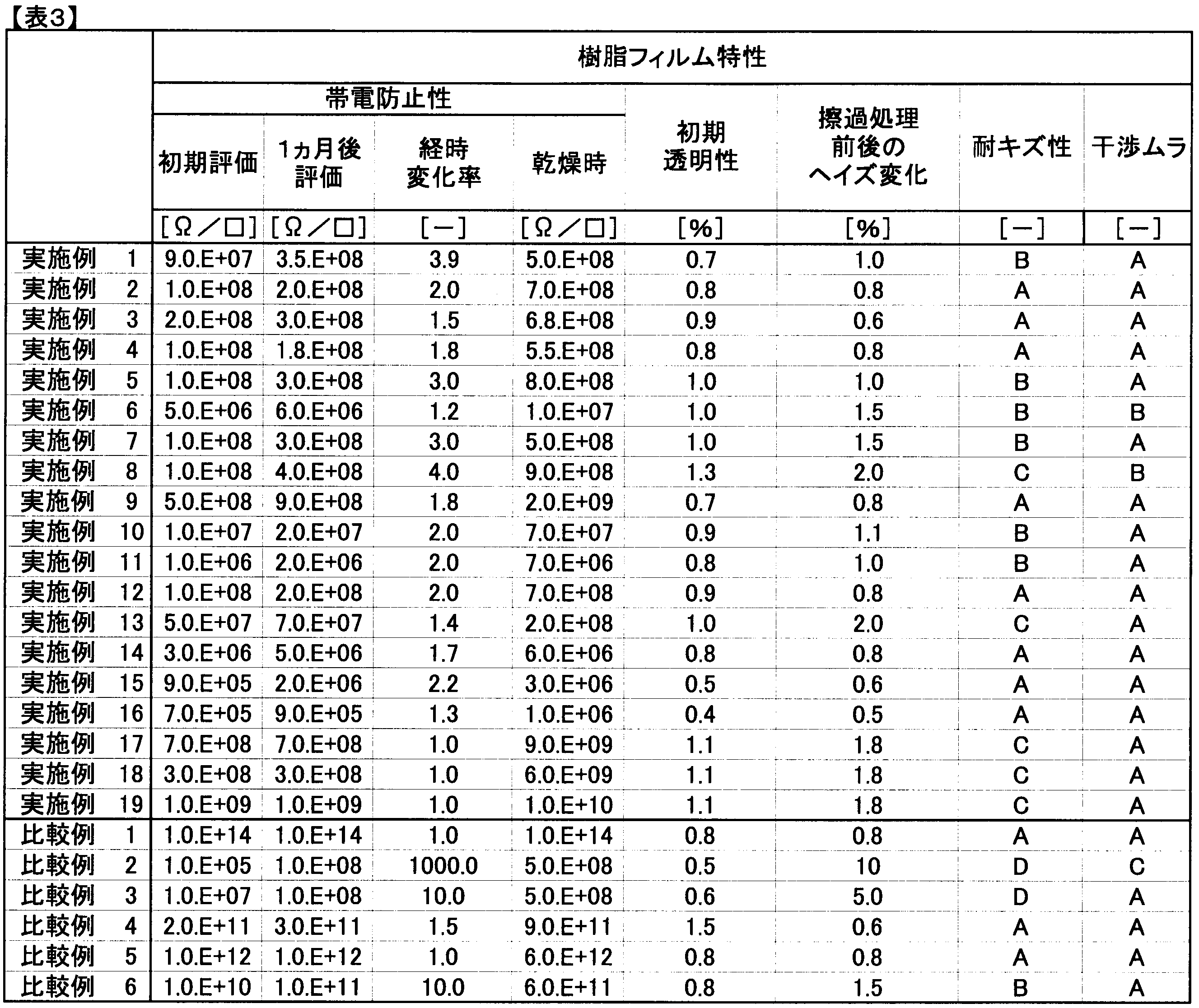
Claims (10)
- 少なくとも一方の表面が、AFM(Atomic Force Microscope(原子間力顕微鏡))の導電測定モード(コンダクティブAFM)により測定される絶縁相(A)と導電相(B)を有し、前記絶縁相(A)と導電相(B)を有する表面を表面αとしたとき、前記表面αにおける絶縁相(A)の占める面積が40%以上80%以下であり、前記表面αの表面抵抗率が1.0×10¹⁰Ω/□以下である樹脂フィルム。
- 前記表面αにおける絶縁相(A)の平均ドメイン径が50nm以上200nm以下である請求項1に記載の樹脂フィルム。
- 前記表面αにおける前記絶縁相(A)の導電性IAと前記導電相(B)の導電性IBの比IA/IBが100以上、100000以下である請求項1または2に記載の樹脂フィルム。
- 前記表面αにおける擦過処理前後のヘイズ変化が3.0%以下である請求項1から3のいずれかに記載の樹脂フィルム。
- 前記表面αにおける、絶縁相(A)の弾性率(GA)が2000MPa以上50000MPa以下である請求項1から4のいずれかに記載の樹脂フィルム。
- 前記表面αにおける、絶縁相(A)の弾性率(GA)と導電相(B)の弾性率(GB)の比、GA/GBが4以上20以下である請求項1から5のいずれかに記載の樹脂フィルム。
- 支持基材とその表面の形成された層(X)を含む2層以上の積層体である請求項1から6のいずれかに記載の樹脂フィルム。
- 前記絶縁相(A)がSi、Al、Ti、Zr,Se、Feからなる群から選ばれる、少なくとも1種の金属元素を含む金属酸化物粒子(a)を含有する請求項1から7のいずれかに記載の樹脂フィルム
- 前記導電相(B)が、ポリチオフェン系導電性化合物(b)とエポキシ樹脂、メラミン樹脂、オキサゾリン化合物、カルボジイミド化合物、イソシアネート化合物から選ばれる少なくとも1種類の架橋剤(c)を含有する請求項1から8のいずれかに記載の樹脂フィルム。
- 請求項1から9のいずれかに記載の樹脂フィルムの製造方法であって、結晶配向が完了する前のポリエステルフィルムの少なくとも片面に、塗料組成物(x)を塗布した後、少なくとも一方向に延伸処理及び熱処理を施す工程を含み、前記塗料組成物(x)が、金属酸化物粒子(a)、導電性成分(b)、エポキシ樹脂、メラミン樹脂、オキサゾリン化合物、カルボジイミド化合物、イソシアネート化合物から選ばれる少なくとも1種類の架橋剤(c)を含有する樹脂フィルムの製造方法。
Priority Applications (3)
| Application Number | Priority Date | Filing Date | Title |
|---|---|---|---|
| CN201980060968.4A CN112739753B (zh) | 2018-10-05 | 2019-08-30 | 树脂膜及其制造方法 |
| KR1020217008096A KR102826914B1 (ko) | 2018-10-05 | 2019-08-30 | 수지 필름 및 그 제조 방법 |
| JP2019547738A JP7419817B2 (ja) | 2018-10-05 | 2019-08-30 | 樹脂フィルムおよびその製造方法 |
Applications Claiming Priority (4)
| Application Number | Priority Date | Filing Date | Title |
|---|---|---|---|
| JP2018-189784 | 2018-10-05 | ||
| JP2018189784 | 2018-10-05 | ||
| JP2019017674 | 2019-02-04 | ||
| JP2019-017674 | 2019-02-04 |
Publications (1)
| Publication Number | Publication Date |
|---|---|
| WO2020071022A1 true WO2020071022A1 (ja) | 2020-04-09 |
Family
ID=70055792
Family Applications (1)
| Application Number | Title | Priority Date | Filing Date |
|---|---|---|---|
| PCT/JP2019/034084 Ceased WO2020071022A1 (ja) | 2018-10-05 | 2019-08-30 | 樹脂フィルムおよびその製造方法 |
Country Status (5)
| Country | Link |
|---|---|
| JP (1) | JP7419817B2 (ja) |
| KR (1) | KR102826914B1 (ja) |
| CN (1) | CN112739753B (ja) |
| TW (1) | TWI848977B (ja) |
| WO (1) | WO2020071022A1 (ja) |
Cited By (1)
| Publication number | Priority date | Publication date | Assignee | Title |
|---|---|---|---|---|
| JP2022065639A (ja) * | 2020-10-15 | 2022-04-27 | 東レ株式会社 | 積層フィルム |
Citations (5)
| Publication number | Priority date | Publication date | Assignee | Title |
|---|---|---|---|---|
| JP2002079617A (ja) * | 2000-07-07 | 2002-03-19 | Teijin Ltd | 帯電防止性積層ポリエステルフィルム |
| JP2003292655A (ja) * | 2002-04-04 | 2003-10-15 | Teijin Dupont Films Japan Ltd | 帯電防止性積層ポリエステルフィルム |
| JP2011227436A (ja) * | 2010-03-30 | 2011-11-10 | Toray Ind Inc | 光学用ポリエステルフィルム |
| WO2016136518A1 (ja) * | 2015-02-27 | 2016-09-01 | 東レ株式会社 | 積層フィルムおよびその製造方法 |
| JP2018086823A (ja) * | 2016-11-30 | 2018-06-07 | 東レ株式会社 | 積層フィルム |
Family Cites Families (7)
| Publication number | Priority date | Publication date | Assignee | Title |
|---|---|---|---|---|
| JPS61204240A (ja) | 1985-03-08 | 1986-09-10 | Diafoil Co Ltd | 二軸延伸ポリエステルフイルム |
| JP4744256B2 (ja) | 2005-09-30 | 2011-08-10 | 三洋電機株式会社 | 室外ユニット |
| KR100699624B1 (ko) * | 2005-11-16 | 2007-03-23 | 주식회사 에이스 디지텍 | 대전방지 고해상 방현 필름의 제조방법 및 이를 이용한 대전방지 고해상 방현 필름 |
| US20100035031A1 (en) | 2006-12-22 | 2010-02-11 | Dai Nippon Printing Co., Ltd. | Optical layered body, method for producing the same, and composition for antistatic layer |
| JP5359652B2 (ja) | 2009-07-29 | 2013-12-04 | 大日本印刷株式会社 | 光学積層体、偏光板及び画像表示装置 |
| JP6070547B2 (ja) * | 2012-03-16 | 2017-02-01 | 東レ株式会社 | 積層フィルムおよびその製造方法 |
| CN104861189B (zh) * | 2015-05-25 | 2018-04-13 | 华南理工大学 | 一种原位合成聚3,4‑乙撑二氧噻吩/纳米金属银透明导电涂层的方法 |
-
2019
- 2019-08-30 JP JP2019547738A patent/JP7419817B2/ja active Active
- 2019-08-30 WO PCT/JP2019/034084 patent/WO2020071022A1/ja not_active Ceased
- 2019-08-30 KR KR1020217008096A patent/KR102826914B1/ko active Active
- 2019-08-30 CN CN201980060968.4A patent/CN112739753B/zh active Active
- 2019-09-17 TW TW108133408A patent/TWI848977B/zh active
Patent Citations (5)
| Publication number | Priority date | Publication date | Assignee | Title |
|---|---|---|---|---|
| JP2002079617A (ja) * | 2000-07-07 | 2002-03-19 | Teijin Ltd | 帯電防止性積層ポリエステルフィルム |
| JP2003292655A (ja) * | 2002-04-04 | 2003-10-15 | Teijin Dupont Films Japan Ltd | 帯電防止性積層ポリエステルフィルム |
| JP2011227436A (ja) * | 2010-03-30 | 2011-11-10 | Toray Ind Inc | 光学用ポリエステルフィルム |
| WO2016136518A1 (ja) * | 2015-02-27 | 2016-09-01 | 東レ株式会社 | 積層フィルムおよびその製造方法 |
| JP2018086823A (ja) * | 2016-11-30 | 2018-06-07 | 東レ株式会社 | 積層フィルム |
Cited By (2)
| Publication number | Priority date | Publication date | Assignee | Title |
|---|---|---|---|---|
| JP2022065639A (ja) * | 2020-10-15 | 2022-04-27 | 東レ株式会社 | 積層フィルム |
| JP7753774B2 (ja) | 2020-10-15 | 2025-10-15 | 東レ株式会社 | 積層フィルム |
Also Published As
| Publication number | Publication date |
|---|---|
| TWI848977B (zh) | 2024-07-21 |
| TW202028317A (zh) | 2020-08-01 |
| KR20210069633A (ko) | 2021-06-11 |
| CN112739753B (zh) | 2023-09-12 |
| CN112739753A (zh) | 2021-04-30 |
| KR102826914B1 (ko) | 2025-06-30 |
| JPWO2020071022A1 (ja) | 2021-09-02 |
| JP7419817B2 (ja) | 2024-01-23 |
Similar Documents
| Publication | Publication Date | Title |
|---|---|---|
| JP7226308B2 (ja) | 積層ポリエステルフィルムおよびその製造方法 | |
| CN105555849B (zh) | 层合膜及其制造方法 | |
| KR20140138643A (ko) | 적층 필름 및 그 제조 방법 | |
| TWI680874B (zh) | 積層薄膜及其製造方法 | |
| CN103796831B (zh) | 涂布膜 | |
| JP7419817B2 (ja) | 樹脂フィルムおよびその製造方法 | |
| KR102537733B1 (ko) | 적층 필름 및 그 제조 방법 | |
| WO2015046137A1 (ja) | 離型フィルム及び基材レス両面粘着シート | |
| JP2021138071A (ja) | 積層フィルムおよびその製造方法 | |
| JP2022152150A (ja) | ガスバリア性フィルム用ベースフィルム、ガスバリア性フィルム用ベースフィルムの製造方法、ガスバリア性フィルム、およびガスバリア性フィルムの製造方法 | |
| JP2015016677A (ja) | 離型ポリエステルフィルム | |
| JP2019048447A (ja) | 積層フィルムおよびその製造方法 | |
| JP2021160175A (ja) | 積層フィルムおよびその製造方法 | |
| JP2015027735A (ja) | 離型ポリエステルフィルム | |
| JP2018122548A (ja) | 積層フィルムおよびその製造方法 | |
| JP6787063B2 (ja) | 積層フィルムおよびその製造方法 | |
| JP2015062998A (ja) | 離型ポリエステルフィルム | |
| JP2015013449A (ja) | 離型ポリエステルフィルム | |
| JP2015027736A (ja) | 離型ポリエステルフィルム | |
| JP2015091904A (ja) | 基材レス両面粘着シート | |
| JP2015063000A (ja) | 離型ポリエステルフィルム | |
| JP2015062999A (ja) | 離型ポリエステルフィルム |
Legal Events
| Date | Code | Title | Description |
|---|---|---|---|
| ENP | Entry into the national phase |
Ref document number: 2019547738 Country of ref document: JP Kind code of ref document: A |
|
| 121 | Ep: the epo has been informed by wipo that ep was designated in this application |
Ref document number: 19869060 Country of ref document: EP Kind code of ref document: A1 |
|
| ENP | Entry into the national phase |
Ref document number: 20217008096 Country of ref document: KR Kind code of ref document: A |
|
| NENP | Non-entry into the national phase |
Ref country code: DE |
|
| 122 | Ep: pct application non-entry in european phase |
Ref document number: 19869060 Country of ref document: EP Kind code of ref document: A1 |