WO2020067537A1 - メタルマスク材料及びその製造方法とメタルマスク - Google Patents
メタルマスク材料及びその製造方法とメタルマスク Download PDFInfo
- Publication number
- WO2020067537A1 WO2020067537A1 PCT/JP2019/038416 JP2019038416W WO2020067537A1 WO 2020067537 A1 WO2020067537 A1 WO 2020067537A1 JP 2019038416 W JP2019038416 W JP 2019038416W WO 2020067537 A1 WO2020067537 A1 WO 2020067537A1
- Authority
- WO
- WIPO (PCT)
- Prior art keywords
- metal mask
- mask material
- plane
- less
- sample
- Prior art date
- Legal status (The legal status is an assumption and is not a legal conclusion. Google has not performed a legal analysis and makes no representation as to the accuracy of the status listed.)
- Ceased
Links
Images


Classifications
-
- C—CHEMISTRY; METALLURGY
- C21—METALLURGY OF IRON
- C21D—MODIFYING THE PHYSICAL STRUCTURE OF FERROUS METALS; GENERAL DEVICES FOR HEAT TREATMENT OF FERROUS OR NON-FERROUS METALS OR ALLOYS; MAKING METAL MALLEABLE, e.g. BY DECARBURISATION OR TEMPERING
- C21D8/00—Modifying the physical properties of ferrous metals or ferrous alloys by deformation combined with, or followed by, heat treatment
- C21D8/02—Modifying the physical properties of ferrous metals or ferrous alloys by deformation combined with, or followed by, heat treatment during manufacturing of plates or strips
- C21D8/0221—Modifying the physical properties of ferrous metals or ferrous alloys by deformation combined with, or followed by, heat treatment during manufacturing of plates or strips characterised by the working steps
- C21D8/0226—Hot rolling
-
- B—PERFORMING OPERATIONS; TRANSPORTING
- B21—MECHANICAL METAL-WORKING WITHOUT ESSENTIALLY REMOVING MATERIAL; PUNCHING METAL
- B21C—MANUFACTURE OF METAL SHEETS, WIRE, RODS, TUBES, PROFILES OR LIKE SEMI-MANUFACTURED PRODUCTS OTHERWISE THAN BY ROLLING; AUXILIARY OPERATIONS USED IN CONNECTION WITH METAL-WORKING WITHOUT ESSENTIALLY REMOVING MATERIAL
- B21C47/00—Winding-up, coiling or winding-off metal wire, metal band or other flexible metal material characterised by features relevant to metal processing only
- B21C47/02—Winding-up or coiling
-
- C—CHEMISTRY; METALLURGY
- C21—METALLURGY OF IRON
- C21D—MODIFYING THE PHYSICAL STRUCTURE OF FERROUS METALS; GENERAL DEVICES FOR HEAT TREATMENT OF FERROUS OR NON-FERROUS METALS OR ALLOYS; MAKING METAL MALLEABLE, e.g. BY DECARBURISATION OR TEMPERING
- C21D1/00—General methods or devices for heat treatment, e.g. annealing, hardening, quenching or tempering
- C21D1/74—Methods of treatment in inert gas, controlled atmosphere, vacuum or pulverulent material
-
- C—CHEMISTRY; METALLURGY
- C21—METALLURGY OF IRON
- C21D—MODIFYING THE PHYSICAL STRUCTURE OF FERROUS METALS; GENERAL DEVICES FOR HEAT TREATMENT OF FERROUS OR NON-FERROUS METALS OR ALLOYS; MAKING METAL MALLEABLE, e.g. BY DECARBURISATION OR TEMPERING
- C21D6/00—Heat treatment of ferrous alloys
- C21D6/001—Heat treatment of ferrous alloys containing Ni
-
- C—CHEMISTRY; METALLURGY
- C21—METALLURGY OF IRON
- C21D—MODIFYING THE PHYSICAL STRUCTURE OF FERROUS METALS; GENERAL DEVICES FOR HEAT TREATMENT OF FERROUS OR NON-FERROUS METALS OR ALLOYS; MAKING METAL MALLEABLE, e.g. BY DECARBURISATION OR TEMPERING
- C21D6/00—Heat treatment of ferrous alloys
- C21D6/007—Heat treatment of ferrous alloys containing Co
-
- C—CHEMISTRY; METALLURGY
- C21—METALLURGY OF IRON
- C21D—MODIFYING THE PHYSICAL STRUCTURE OF FERROUS METALS; GENERAL DEVICES FOR HEAT TREATMENT OF FERROUS OR NON-FERROUS METALS OR ALLOYS; MAKING METAL MALLEABLE, e.g. BY DECARBURISATION OR TEMPERING
- C21D8/00—Modifying the physical properties of ferrous metals or ferrous alloys by deformation combined with, or followed by, heat treatment
- C21D8/02—Modifying the physical properties of ferrous metals or ferrous alloys by deformation combined with, or followed by, heat treatment during manufacturing of plates or strips
-
- C—CHEMISTRY; METALLURGY
- C21—METALLURGY OF IRON
- C21D—MODIFYING THE PHYSICAL STRUCTURE OF FERROUS METALS; GENERAL DEVICES FOR HEAT TREATMENT OF FERROUS OR NON-FERROUS METALS OR ALLOYS; MAKING METAL MALLEABLE, e.g. BY DECARBURISATION OR TEMPERING
- C21D8/00—Modifying the physical properties of ferrous metals or ferrous alloys by deformation combined with, or followed by, heat treatment
- C21D8/02—Modifying the physical properties of ferrous metals or ferrous alloys by deformation combined with, or followed by, heat treatment during manufacturing of plates or strips
- C21D8/0221—Modifying the physical properties of ferrous metals or ferrous alloys by deformation combined with, or followed by, heat treatment during manufacturing of plates or strips characterised by the working steps
- C21D8/0236—Cold rolling
-
- C—CHEMISTRY; METALLURGY
- C21—METALLURGY OF IRON
- C21D—MODIFYING THE PHYSICAL STRUCTURE OF FERROUS METALS; GENERAL DEVICES FOR HEAT TREATMENT OF FERROUS OR NON-FERROUS METALS OR ALLOYS; MAKING METAL MALLEABLE, e.g. BY DECARBURISATION OR TEMPERING
- C21D8/00—Modifying the physical properties of ferrous metals or ferrous alloys by deformation combined with, or followed by, heat treatment
- C21D8/02—Modifying the physical properties of ferrous metals or ferrous alloys by deformation combined with, or followed by, heat treatment during manufacturing of plates or strips
- C21D8/0221—Modifying the physical properties of ferrous metals or ferrous alloys by deformation combined with, or followed by, heat treatment during manufacturing of plates or strips characterised by the working steps
- C21D8/0242—Flattening; Dressing; Flexing
-
- C—CHEMISTRY; METALLURGY
- C21—METALLURGY OF IRON
- C21D—MODIFYING THE PHYSICAL STRUCTURE OF FERROUS METALS; GENERAL DEVICES FOR HEAT TREATMENT OF FERROUS OR NON-FERROUS METALS OR ALLOYS; MAKING METAL MALLEABLE, e.g. BY DECARBURISATION OR TEMPERING
- C21D8/00—Modifying the physical properties of ferrous metals or ferrous alloys by deformation combined with, or followed by, heat treatment
- C21D8/02—Modifying the physical properties of ferrous metals or ferrous alloys by deformation combined with, or followed by, heat treatment during manufacturing of plates or strips
- C21D8/0247—Modifying the physical properties of ferrous metals or ferrous alloys by deformation combined with, or followed by, heat treatment during manufacturing of plates or strips characterised by the heat treatment
- C21D8/0252—Modifying the physical properties of ferrous metals or ferrous alloys by deformation combined with, or followed by, heat treatment during manufacturing of plates or strips characterised by the heat treatment with application of tension
-
- C—CHEMISTRY; METALLURGY
- C21—METALLURGY OF IRON
- C21D—MODIFYING THE PHYSICAL STRUCTURE OF FERROUS METALS; GENERAL DEVICES FOR HEAT TREATMENT OF FERROUS OR NON-FERROUS METALS OR ALLOYS; MAKING METAL MALLEABLE, e.g. BY DECARBURISATION OR TEMPERING
- C21D8/00—Modifying the physical properties of ferrous metals or ferrous alloys by deformation combined with, or followed by, heat treatment
- C21D8/02—Modifying the physical properties of ferrous metals or ferrous alloys by deformation combined with, or followed by, heat treatment during manufacturing of plates or strips
- C21D8/0247—Modifying the physical properties of ferrous metals or ferrous alloys by deformation combined with, or followed by, heat treatment during manufacturing of plates or strips characterised by the heat treatment
- C21D8/0268—Modifying the physical properties of ferrous metals or ferrous alloys by deformation combined with, or followed by, heat treatment during manufacturing of plates or strips characterised by the heat treatment between cold rolling steps
-
- C—CHEMISTRY; METALLURGY
- C21—METALLURGY OF IRON
- C21D—MODIFYING THE PHYSICAL STRUCTURE OF FERROUS METALS; GENERAL DEVICES FOR HEAT TREATMENT OF FERROUS OR NON-FERROUS METALS OR ALLOYS; MAKING METAL MALLEABLE, e.g. BY DECARBURISATION OR TEMPERING
- C21D8/00—Modifying the physical properties of ferrous metals or ferrous alloys by deformation combined with, or followed by, heat treatment
- C21D8/02—Modifying the physical properties of ferrous metals or ferrous alloys by deformation combined with, or followed by, heat treatment during manufacturing of plates or strips
- C21D8/0247—Modifying the physical properties of ferrous metals or ferrous alloys by deformation combined with, or followed by, heat treatment during manufacturing of plates or strips characterised by the heat treatment
- C21D8/0273—Final recrystallisation annealing
-
- C—CHEMISTRY; METALLURGY
- C21—METALLURGY OF IRON
- C21D—MODIFYING THE PHYSICAL STRUCTURE OF FERROUS METALS; GENERAL DEVICES FOR HEAT TREATMENT OF FERROUS OR NON-FERROUS METALS OR ALLOYS; MAKING METAL MALLEABLE, e.g. BY DECARBURISATION OR TEMPERING
- C21D8/00—Modifying the physical properties of ferrous metals or ferrous alloys by deformation combined with, or followed by, heat treatment
- C21D8/02—Modifying the physical properties of ferrous metals or ferrous alloys by deformation combined with, or followed by, heat treatment during manufacturing of plates or strips
- C21D8/0278—Modifying the physical properties of ferrous metals or ferrous alloys by deformation combined with, or followed by, heat treatment during manufacturing of plates or strips involving a particular surface treatment
-
- C—CHEMISTRY; METALLURGY
- C21—METALLURGY OF IRON
- C21D—MODIFYING THE PHYSICAL STRUCTURE OF FERROUS METALS; GENERAL DEVICES FOR HEAT TREATMENT OF FERROUS OR NON-FERROUS METALS OR ALLOYS; MAKING METAL MALLEABLE, e.g. BY DECARBURISATION OR TEMPERING
- C21D9/00—Heat treatment, e.g. annealing, hardening, quenching or tempering, adapted for particular articles; Furnaces therefor
- C21D9/46—Heat treatment, e.g. annealing, hardening, quenching or tempering, adapted for particular articles; Furnaces therefor for sheet metals
-
- C—CHEMISTRY; METALLURGY
- C22—METALLURGY; FERROUS OR NON-FERROUS ALLOYS; TREATMENT OF ALLOYS OR NON-FERROUS METALS
- C22C—ALLOYS
- C22C38/00—Ferrous alloys, e.g. steel alloys
- C22C38/002—Ferrous alloys, e.g. steel alloys containing In, Mg, or other elements not provided for in one single group C22C38/001 - C22C38/60
-
- C—CHEMISTRY; METALLURGY
- C22—METALLURGY; FERROUS OR NON-FERROUS ALLOYS; TREATMENT OF ALLOYS OR NON-FERROUS METALS
- C22C—ALLOYS
- C22C38/00—Ferrous alloys, e.g. steel alloys
- C22C38/02—Ferrous alloys, e.g. steel alloys containing silicon
-
- C—CHEMISTRY; METALLURGY
- C22—METALLURGY; FERROUS OR NON-FERROUS ALLOYS; TREATMENT OF ALLOYS OR NON-FERROUS METALS
- C22C—ALLOYS
- C22C38/00—Ferrous alloys, e.g. steel alloys
- C22C38/04—Ferrous alloys, e.g. steel alloys containing manganese
-
- C—CHEMISTRY; METALLURGY
- C22—METALLURGY; FERROUS OR NON-FERROUS ALLOYS; TREATMENT OF ALLOYS OR NON-FERROUS METALS
- C22C—ALLOYS
- C22C38/00—Ferrous alloys, e.g. steel alloys
- C22C38/06—Ferrous alloys, e.g. steel alloys containing aluminium
-
- C—CHEMISTRY; METALLURGY
- C22—METALLURGY; FERROUS OR NON-FERROUS ALLOYS; TREATMENT OF ALLOYS OR NON-FERROUS METALS
- C22C—ALLOYS
- C22C38/00—Ferrous alloys, e.g. steel alloys
- C22C38/08—Ferrous alloys, e.g. steel alloys containing nickel
-
- C—CHEMISTRY; METALLURGY
- C22—METALLURGY; FERROUS OR NON-FERROUS ALLOYS; TREATMENT OF ALLOYS OR NON-FERROUS METALS
- C22C—ALLOYS
- C22C38/00—Ferrous alloys, e.g. steel alloys
- C22C38/10—Ferrous alloys, e.g. steel alloys containing cobalt
-
- C—CHEMISTRY; METALLURGY
- C22—METALLURGY; FERROUS OR NON-FERROUS ALLOYS; TREATMENT OF ALLOYS OR NON-FERROUS METALS
- C22C—ALLOYS
- C22C38/00—Ferrous alloys, e.g. steel alloys
- C22C38/10—Ferrous alloys, e.g. steel alloys containing cobalt
- C22C38/105—Ferrous alloys, e.g. steel alloys containing cobalt containing Co and Ni
-
- C—CHEMISTRY; METALLURGY
- C23—COATING METALLIC MATERIAL; COATING MATERIAL WITH METALLIC MATERIAL; CHEMICAL SURFACE TREATMENT; DIFFUSION TREATMENT OF METALLIC MATERIAL; COATING BY VACUUM EVAPORATION, BY SPUTTERING, BY ION IMPLANTATION OR BY CHEMICAL VAPOUR DEPOSITION, IN GENERAL; INHIBITING CORROSION OF METALLIC MATERIAL OR INCRUSTATION IN GENERAL
- C23C—COATING METALLIC MATERIAL; COATING MATERIAL WITH METALLIC MATERIAL; SURFACE TREATMENT OF METALLIC MATERIAL BY DIFFUSION INTO THE SURFACE, BY CHEMICAL CONVERSION OR SUBSTITUTION; COATING BY VACUUM EVAPORATION, BY SPUTTERING, BY ION IMPLANTATION OR BY CHEMICAL VAPOUR DEPOSITION, IN GENERAL
- C23C14/00—Coating by vacuum evaporation, by sputtering or by ion implantation of the coating forming material
- C23C14/04—Coating on selected surface areas, e.g. using masks
- C23C14/042—Coating on selected surface areas, e.g. using masks using masks
-
- C—CHEMISTRY; METALLURGY
- C23—COATING METALLIC MATERIAL; COATING MATERIAL WITH METALLIC MATERIAL; CHEMICAL SURFACE TREATMENT; DIFFUSION TREATMENT OF METALLIC MATERIAL; COATING BY VACUUM EVAPORATION, BY SPUTTERING, BY ION IMPLANTATION OR BY CHEMICAL VAPOUR DEPOSITION, IN GENERAL; INHIBITING CORROSION OF METALLIC MATERIAL OR INCRUSTATION IN GENERAL
- C23C—COATING METALLIC MATERIAL; COATING MATERIAL WITH METALLIC MATERIAL; SURFACE TREATMENT OF METALLIC MATERIAL BY DIFFUSION INTO THE SURFACE, BY CHEMICAL CONVERSION OR SUBSTITUTION; COATING BY VACUUM EVAPORATION, BY SPUTTERING, BY ION IMPLANTATION OR BY CHEMICAL VAPOUR DEPOSITION, IN GENERAL
- C23C16/00—Chemical coating by decomposition of gaseous compounds, without leaving reaction products of surface material in the coating, i.e. chemical vapour deposition [CVD] processes
- C23C16/04—Coating on selected surface areas, e.g. using masks
- C23C16/042—Coating on selected surface areas, e.g. using masks using masks
-
- C—CHEMISTRY; METALLURGY
- C23—COATING METALLIC MATERIAL; COATING MATERIAL WITH METALLIC MATERIAL; CHEMICAL SURFACE TREATMENT; DIFFUSION TREATMENT OF METALLIC MATERIAL; COATING BY VACUUM EVAPORATION, BY SPUTTERING, BY ION IMPLANTATION OR BY CHEMICAL VAPOUR DEPOSITION, IN GENERAL; INHIBITING CORROSION OF METALLIC MATERIAL OR INCRUSTATION IN GENERAL
- C23F—NON-MECHANICAL REMOVAL OF METALLIC MATERIAL FROM SURFACE; INHIBITING CORROSION OF METALLIC MATERIAL OR INCRUSTATION IN GENERAL; MULTI-STEP PROCESSES FOR SURFACE TREATMENT OF METALLIC MATERIAL INVOLVING AT LEAST ONE PROCESS PROVIDED FOR IN CLASS C23 AND AT LEAST ONE PROCESS COVERED BY SUBCLASS C21D OR C22F OR CLASS C25
- C23F1/00—Etching metallic material by chemical means
- C23F1/02—Local etching
-
- C—CHEMISTRY; METALLURGY
- C21—METALLURGY OF IRON
- C21D—MODIFYING THE PHYSICAL STRUCTURE OF FERROUS METALS; GENERAL DEVICES FOR HEAT TREATMENT OF FERROUS OR NON-FERROUS METALS OR ALLOYS; MAKING METAL MALLEABLE, e.g. BY DECARBURISATION OR TEMPERING
- C21D2201/00—Treatment for obtaining particular effects
- C21D2201/05—Grain orientation
-
- H—ELECTRICITY
- H10—SEMICONDUCTOR DEVICES; ELECTRIC SOLID-STATE DEVICES NOT OTHERWISE PROVIDED FOR
- H10K—ORGANIC ELECTRIC SOLID-STATE DEVICES
- H10K71/00—Manufacture or treatment specially adapted for the organic devices covered by this subclass
- H10K71/10—Deposition of organic active material
- H10K71/16—Deposition of organic active material using physical vapour deposition [PVD], e.g. vacuum deposition or sputtering
- H10K71/166—Deposition of organic active material using physical vapour deposition [PVD], e.g. vacuum deposition or sputtering using selective deposition, e.g. using a mask
-
- H—ELECTRICITY
- H10—SEMICONDUCTOR DEVICES; ELECTRIC SOLID-STATE DEVICES NOT OTHERWISE PROVIDED FOR
- H10K—ORGANIC ELECTRIC SOLID-STATE DEVICES
- H10K71/00—Manufacture or treatment specially adapted for the organic devices covered by this subclass
- H10K71/40—Thermal treatment, e.g. annealing in the presence of a solvent vapour
Definitions
- the present invention relates to a metal mask material and a metal mask used in the manufacture of an organic EL display (OLED) and the like.
- the metal mask for the OLED is fixed in a state in which tension is added to the window frame-shaped frame so as not to be warped or sagged. As shown in FIG. Alternatively, it is deposited on a substrate 2 such as a film substrate.
- the metal mask has a mask hole formed so as to correspond to RGB of the pixel of the OLED at a ratio of 1: 1 and includes a plurality of mask portions having the same size as the OLED at equal intervals.
- the metal mask it is necessary to form the mask holes so as to correspond to the RGB of the pixels of the OLED to be manufactured at a ratio of 1: 1. Therefore, the pitch interval between the mask holes 1a is at least as large as the pixel density of the OLED. And the hole diameter of the mask hole 1a is also reduced accordingly.
- the thickness of the metal mask inhibits the organic EL light emitting material 3a from being deposited on the substrate 2, thereby forming RGB.
- Some of the sub-pixels may be formed thinner than a desired thickness.
- a metal plate having a thickness approximately equal to the pitch interval is used for the metal mask 1.
- one surface of the metal plate is so shaped that the hole diameter of the mask hole 1a has a cross-sectional shape that expands from the substrate 2 side toward the evaporation source 3 side of the organic EL light emitting material 3a.
- the metal mask 1 is manufactured by etching about 30 to 70% of the plate thickness from below (hereinafter, referred to as “half etching”).
- Patent Document 6 discloses that an internal stress of a metal plate is removed by an annealing process, a sample taken out of the metal plate after the annealing process is etched, and whether or not the curvature k of the warp is 0.008 mm ⁇ 1 or less.
- a manufacturing method including a step of inspecting is disclosed. However, the inspection step is merely a step of selecting a long metal plate for obtaining a vapor deposition mask having good vapor deposition characteristics from a plurality of manufactured long metal plates. It does not disclose a method for specifying a metal structure of a metal plate. Therefore, in the manufacturing method disclosed in Patent Document 6, it is difficult to specify manufacturing conditions for controlling the residual stress of the metal plate in an appropriate range before manufacturing the long metal plate.
- Patent Document 7 discloses a manufacturing method including an inspection step of inspecting the degree of thermal recovery before and after performing a heat treatment on a sample taken from a manufactured long metal plate in order to solve such a technical problem. I do.
- the inspection process disclosed in Patent Literature 7 is based on using a long metal plate having a small residual strain and a small variation as a long metal plate as a base of a vapor deposition mask. Does not disclose a method of identifying Therefore, in the manufacturing method disclosed in Patent Document 7, it is difficult to specify manufacturing conditions for controlling the residual stress of the metal plate in an appropriate range before manufacturing the long metal plate.
- Patent Document 8 discloses that the X-ray diffraction intensities of the main crystal orientations (111), (200), (220), and (311) of the rolled surface are within a certain range in consideration of the fact that the etching rate varies depending on the crystal orientation.
- a metal mask material made of an Fe—Ni-based alloy satisfying the following relationship is disclosed.
- the metal mask material disclosed in Patent Document 8 is characterized in that it can be etched uniformly and accurately because it is not strongly oriented only in a specific direction.
- Patent Document 8 discloses that the degree of orientation of (200), (220), and (311) of the metal mask material includes the degree of cold rolling before the final recrystallization annealing, the crystal grain size number of the final recrystallization annealing, and the final cold rolling.
- Patent Document 9 a sample having a length of 150 mm and a width of 30 mm is cut out, the sample is etched from one side, and the amount of warpage when 60% of the thickness of the sample is removed is 15 mm or less.
- a metal mask material that is at least 01 mm and less than 0.10 mm.
- the patent document does not disclose reducing the amount of warpage from the viewpoint of the fine structure of the metal mask.
- JP-A-2004-183023 JP-A-2017-88915 International Publication No. 00/70108 JP-A-2003-27188 JP 2004-115905 A JP 2014-101543 A JP-A-2015-78401 JP 2014-101543 A International Publication No. WO2018 / 043641
- the present invention has been made in view of such a problem, and an object of the present invention is to provide a metal mask material for an OLED in which the amount of warpage is reduced, a manufacturing method thereof, and a metal mask.
- the gist of the present invention for solving the above problems is as follows.
- (1) In mass%, Ni: 35.0 to 37.0%, Co: 0.00 to 0.50%, the balance being Fe and impurities, A metal mask material having a thickness of 5.00 ⁇ m or more and 50.00 ⁇ m or less, A sample of the metal mask material having a square shape of 100 mm on a side is etched from one side thereof until the thickness of the sample becomes 2/5, and the sample obtained when the etched sample is placed on a surface plate 3.
- the metal mask material according to claim 1 wherein the maximum amount of warpage of the four corners is 5.0 mm or less.
- (2) The metal mask material according to (1), further containing, by mass%, C: 0.05% or less and Ca: 0.0005% or less.
- the impurities are: Si: 0.30% or less, Mn: 0.70% or less, Al: 0.01% or less, Mg: 0.0005% or less, P: 0.030% or less, S: 0
- the average lattice spacing of ⁇ 111 ⁇ planes from 1.45 ⁇ m to 7.11 ⁇ m below the surface satisfies the following formulas (1-1) and (1-2).
- the metal mask material according to any one of (3). ⁇ D ⁇ 0.00030 (1-1) ⁇ D
- the definition of D M and D L in the above formulas are as follows.
- D M average lattice spacing (unit: nm) of ⁇ 111 ⁇ plane obtained by oblique incidence X-ray diffraction
- D L Reference value of lattice spacing of ⁇ 111 ⁇ plane (unit: nm) or average lattice spacing of ⁇ 111 ⁇ plane calculated from average lattice constant of bulk (unit: nm)
- H w111 in the above formula is an average half width of the ⁇ 111 ⁇ plane from 1.45 ⁇ m to 7.11 ⁇ m below the surface, obtained by oblique incidence X-ray diffraction
- t is a plate of the metal mask material.
- I 311 is the diffraction intensity of the ⁇ 311 ⁇ plane.
- R in the above formula is a residual stress value measured by using the X-ray stress measurement method, and ⁇ is the X-ray stress value. This is an error calculated when a residual stress value is measured using a stress measurement method.
- the present invention it is possible to provide a metal mask material having a small amount of warpage and capable of performing precise etching corresponding to a higher pixel density of an OLED, and a metal mask using the metal mask material.
- 11 is a graph showing the relationship between the average lattice spacing of ⁇ 111 ⁇ planes from the surface of the metal mask material of the production example to 10.0 ⁇ m and the amount of warpage of the metal mask material.
- 11 is a graph showing the relationship between the average value of the half width of the diffraction peak on the ⁇ 111 ⁇ plane from the surface of the metal mask material of the production example to 7.0 ⁇ m and the amount of warpage of the metal mask material. It is the schematic explaining the influence which a uniform distortion gives to the diffraction angle in an X-ray diffraction peak, and the influence which a non-uniform distortion gives to the half value width of an X-ray diffraction peak.
- (A) and (B) are X-ray diffraction patterns measured by oblique incidence X-ray diffraction by changing the incident angle of X-rays on the surface of the metal mask material.
- (A) is an X-ray diffraction pattern of a metal mask material observed based on the X-ray diffraction method of the concentrated optical system
- (B) is a measurement result of the X-ray diffraction method of the concentrated optical system. It is a graph of the relationship between the average distance of the obtained ⁇ 200 ⁇ plane, and the amount of said warpage.
- a depth r from the surface of the metal mask material to 7.0 ⁇ m and a ratio r (r I 111 / I 200 ) of the integrated intensity I 111 of the ⁇ 111 ⁇ plane to the integrated intensity I 200 of the ⁇ 200 ⁇ plane.
- 6 is a graph showing a relationship with the graph.
- 9 is a graph showing a relationship between r max and the amount of warpage of a metal mask material.
- A) is a graph showing the relationship between the value of r (1) and the amount of warpage of each production example
- (B) is a graph showing the relationship between the value of r (2) and the amount of warpage of each production example.
- (C) is a graph which shows the relationship between the value of r (3) of each manufacture example, and the amount of curvature.
- (A) and (b) show sample Nos.
- each of the graphs is plotted on a graph in which the vertical axis is a value of “2 ⁇ (deg)” and the horizontal axis is a value of “sin 2 ⁇ ”.
- FIG. 10 is a graph plotting residual stress values calculated from X-ray diffraction peaks on the ⁇ 220 ⁇ plane using an X-ray diffraction method of a concentrated optical system and errors in residual stress values for each of a to e.
- (A) and (b) show sample Nos.
- each of the graphs is plotted on a graph in which the vertical axis is a value of “2 ⁇ (deg)” and the horizontal axis is a value of “sin 2 ⁇ ”.
- Sample No. 9 is a graph plotting the values of sin 2 [psi as coordinates in ⁇ 220 ⁇ diffraction peak position of the plane (2 ⁇ (deg)) and the [psi angles in the [psi angles.
- Sample No. 9 is a graph showing the relationship between the parameters b and c of the approximate curve (6-5) and the amount of warpage for each of a to e.
- Sample No. 9 is a graph showing the relationship between the parameters d and e of the approximate curve (6-5) and the amount of warp for each of a to e. It is a graph which shows the relationship between each final annealing temperature of the metal mask material of a manufacture example, and oxide film thickness.
- FIG. 4 is a graph showing a depth profile of an oxygen concentration from a surface of a metal mask material measured using an Auger electron spectrometer.
- FIG. 3 is a schematic explanatory view showing a step of depositing an organic EL light emitting material on a substrate and a use state of a metal mask in the step.
- the metal mask material of the present invention contains the following components, with the balance being iron and impurities.
- Nickel (Ni) is a main component for suppressing the coefficient of thermal expansion of the alloy to be low, and therefore, it is necessary to adjust the Ni content to 35.00% or more. However, if the Ni content is too high, a bainite structure is likely to be formed in the steel after hot rolling or hot forging. Therefore, the Ni content is 37.0% or less.
- a part of iron may be changed to the following composition from the viewpoint of reducing inclusions such as spinel.
- the contents of C, Ca, Mn, Si, Mg and Al may be 0%.
- Carbon (C) increases the strength of the metal mask material. However, if C is excessively contained, inclusions derived from carbides of the alloy increase. Therefore, the C content that may be contained in the metal mask material is preferably set to 0.05% or less.
- Ca forms a solid solution in the sulfide, finely disperses the sulfide, and makes the shape of the sulfide spherical. If the Ca content is too low, that is, if the Ca content with respect to the S content is too low, Ca does not easily form a solid solution with the sulfide, and the sulfide does not easily become spheroidized. On the other hand, if the Ca content is too large, the Ca content relative to the S content is too high, and Ca that did not form a solid solution with the sulfide may form a coarse oxide, resulting in poor etching. Therefore, the Ca content is preferably set to 0.0005% or less. The preferable range of the Ca amount is 0.0001% or less.
- Mn 0 to 0.70%
- Manganese (Mn) is actively used as a deoxidizer instead of Mg and Al to avoid spinel formation.
- the Mn content is preferably set to 0.70% or less.
- the preferred range of the Mn content is 0.30% or less.
- Si Silicon (Si) is positively deoxidized by Mn and Si instead of deoxidized by Mg and Al in order to avoid generation of spinel.
- Si increases the coefficient of thermal expansion of the alloy.
- the metal mask material may be used under a temperature environment of about 200 ° C. so that the organic EL light emitting material emitted from the evaporation source can pass through the mask hole. Therefore, in the metal mask material of the present invention, Si is limited to 0.30% or less.
- MnO—SiO 2 as a deoxidation product is a vitrified soft inclusion, which is stretched and divided during hot rolling to be refined. Therefore, the hydrogen embrittlement resistance is enhanced.
- the Si content exceeds 0.30%, the strength becomes too high. In this case, the workability of the alloy decreases.
- the preferable range of the Si content is set to 0.01% or less.
- Mg Magnesium (Mg) deoxidizes steel. However, if the Mg content exceeds 0.0005%, coarse inclusions may be generated, resulting in poor etching. Further, it is preferable that the content of Mg is low in order to avoid formation of spinel. Therefore, the Mg content is preferably set to 0.0001% or less.
- Al deoxidizes steel.
- the Al content exceeds 0.010%, coarse inclusions may be generated, resulting in poor etching.
- the content of Al is preferably small in order to avoid the formation of spinel. Therefore, the preferable range of the Al content is set to 0.001% or less.
- the composition of the metal mask material of the present invention includes components such as P and S as impurities.
- the content of impurities is limited within the following range.
- P 0.030% or less; S: 0.015% or less
- P and S are elements that form inclusions by combining with alloying elements such as Mn in the metal mask material
- P is limited to 0.030% or less and S: 0.015% or less.
- P 0.003% or less and S: 0.0015% or less.
- the present invention can be applied to a metal mask material having a plate thickness of 50.00 ⁇ m or less, similarly to a normal mask material. Since it is required to form a high-definition pattern, the plate thickness tends to be thin. That is, the present invention can be applied to a metal mask material having a plate thickness of 30.00 ⁇ m or less, 25.00 ⁇ m or less, 20.00 ⁇ m or less, 15.00 ⁇ m or less, and 10.00 ⁇ m or less.
- the lower limit is not particularly limited, but may be 5.00 ⁇ m for reasons of production by rolling.
- a 100-mm square sample is cut out of a metal mask material, and one-sided surface of the sample is etched to remove 3/5 of the thickness of the sample.
- the sample after etching is placed on a surface plate. Place.
- the maximum value of the floating amount of the placed sample from the square platen is defined as the amount of warpage of the metal mask material.
- the etching method is not particularly limited, the sample may be immersed in an etching solution such as an aqueous solution of ferric chloride after protecting one surface of the sample with a resist.
- the lower the amount of warpage the better, and it may be 5.0 mm or less.
- the upper limit of the amount of warpage may be 4.5 mm, 4.0 mm, 3.5 mm, 3.0 mm, 2.5 mm, 2.0 mm, 1.5 mm, 1.0 mm, and 0.5 mm.
- the amount of warpage can be evaluated in a state that is closest to the actual state of etching at the time of manufacture of a mask when measured on a surface plate.
- a state that is closest to the actual state of etching at the time of manufacture of a mask when measured on a surface plate.
- the amount of warpage there is an example in which the upper end of a strip-shaped cut sample is suspended in contact with a vertical surface plate, and the distance (horizontal distance) at which the lower end of the cut sample is away from the vertical surface plate is defined as the amount of warpage (Patent Document 9) .
- the amount of warpage on the surface cannot be evaluated (three-dimensional evaluation).
- the metal mask material Before half-etching, the metal mask material is flat and has no deformation, but after half-etching, the above-described warpage occurs. On the other hand, before and after half-etching the metal mask material, the thickness of the metal mask material changes and the balance of the residual stress of the metal mask material changes, so that the strain distribution in the thickness direction and the amount of warpage are related. .
- the present inventors thought that, if a parameter directly or indirectly related to the strain in the thickness direction of the metal mask material was specified, the residual stress of the metal mask material could be controlled by controlling the parameter. Therefore, the embodiment of the present invention is characterized in that the amount of warpage is suppressed by controlling a parameter directly or indirectly related to the strain in the thickness direction of the metal mask material.
- the slip plane is a ⁇ 111 ⁇ plane. From this, the present inventors believe that the ⁇ 111 ⁇ plane spacing in the thickness direction of the metal mask material is related to the distribution of uniform strain in the thickness direction, and consider the ⁇ 111 ⁇ plane in the thickness direction of the metal mask material. We conducted intensive research on the relationship between the interval and the amount of warpage after half-etching.
- the average lattice spacing of the ⁇ 111 ⁇ plane measured by oblique incidence X-ray diffraction in the thickness direction, and the average lattice spacing of the ⁇ 111 ⁇ plane calculated from the average lattice constant of the bulk The present inventors have found that a metal mask material is manufactured so that the difference between the two can be reduced, and the amount of warpage can be reduced by using the metal mask material.
- the first embodiment is based on this finding.
- the sample No. The metal mask materials a to e were manufactured. For each of these metal mask materials, the lattice spacing of the ⁇ 111 ⁇ plane in the thickness direction was measured under the following conditions.
- sample No. In the compositions a to e the Ni content is 36.0%, and the balance is iron and impurities.
- the contents of impurities such as Al, Mg, Mn, Si, P, and S were all below the detection limit.
- the “final annealing temperature (° C.)” in Table 1 is an annealing temperature in a tension annealing step performed after the final rolling step.
- the annealing temperature in the tension annealing step performed after the final rolling step is referred to as “final annealing temperature (° C.)”.
- the lattice spacing of the ⁇ 111 ⁇ plane in the thickness direction was measured by oblique incidence X-ray diffraction.
- the cathode of the X-ray diffractometer was Co, and the tube voltage and current at the time of measurement were 40 kV and 135 mA, respectively.
- the oblique incidence X-ray diffraction method is performed by using a parallel beam optical system of Rigaku SmartLab, and the optical axis of the incident X-ray is at an angle ( ⁇ ) of 0.2 ° or 0.4 ° with respect to the surface of the sample.
- the X-ray mass absorption coefficient was converted into the penetration depth in the direction perpendicular to the surface.
- FIG. 1 shows measurement results of the penetration depth (depth from the surface) in the direction perpendicular to the surface measured for each of the incident angles of the parallel beam optical system and the lattice spacing of the ⁇ 111 ⁇ plane at the depth position. .
- the change in the lattice spacing of the ⁇ 111 ⁇ plane is large. All of the metal mask materials a to e have similar changes.
- the lattice spacing of the ⁇ 111 ⁇ plane is more stable than the change in the lattice spacing of the ⁇ 111 ⁇ plane in the region from the surface to 1 ⁇ m.
- the sample changes differently depending on the sample.
- the average lattice spacing (unit: nm) of ⁇ 111 ⁇ planes obtained by the oblique incidence X-ray diffraction method refers to the lattice spacing of the ⁇ 111 ⁇ plane in a region having a depth of 1.0 ⁇ m or more below the surface. It is determined by directly measuring and averaging each depth by the incident X-ray diffraction method.
- the depth at which the lattice spacing of the ⁇ 111 ⁇ plane is measured by the oblique incidence X-ray diffraction method is preferably from 1.45 ⁇ m to 7.11 ⁇ m below the surface.
- FIG. 9 For each of the metal mask materials a, b, c, d, and e, an average lattice spacing of ⁇ 111 ⁇ planes obtained by measuring from the surface to 10.0 ⁇ m using an oblique incidence X-ray diffraction method; 9 is a graph showing a relationship with a warpage amount. As can be seen from FIG. 3, the amount of warpage decreases as the average lattice spacing of the ⁇ 111 ⁇ plane obtained by measurement using the oblique incidence X-ray diffraction method increases.
- the reference value of the lattice spacing of the ⁇ 111 ⁇ plane of the metal mask material (Fe-36 mass% Ni) of a, b, c, d, and e is the lattice of the ⁇ 111 ⁇ plane where the amount of warpage after half-etching is zero.
- the surface spacing was used.
- the reference value of the lattice spacing of the ⁇ 111 ⁇ plane is obtained by approximating the measured value of the amount of warpage of these samples by an exponential function using the average lattice spacing of the ⁇ 111 ⁇ plane as a parameter.
- the value on the horizontal axis of the approximate curve where the value on the vertical axis (the amount of warpage) is 0 is the reference value for the lattice spacing of the ⁇ 111 ⁇ plane.
- the sample No. The reference value of the lattice spacing between the ⁇ 111 ⁇ planes of the metal mask materials a, b, c, d, and e is 0.20763 nm.
- ⁇ D) is 0.00030 nm or less, and the amount of warpage is reduced to 5.0 mm or less.
- the sample No. was used as a reference value of the lattice spacing of the ⁇ 111 ⁇ plane.
- the average lattice spacing of ⁇ 111 ⁇ planes calculated from the average lattice constant of each bulk obtained by measuring the metal mask materials a, b, c, d, and e by the concentration method may be used.
- the diffraction pattern of the ⁇ 111 ⁇ plane cannot be directly observed by the X-ray diffraction method using the concentration method.
- the average lattice constant of the bulk of the alloy constituting the metal mask material is measured by using the X-ray diffraction method using the concentration method, and the ⁇ 111 ⁇ plane of the ⁇ 111 ⁇ plane is determined from the average lattice constant of the bulk by the following means.
- the average lattice plane spacing ( DL (unit: nm)) is calculated.
- the value of the Nelson-Riley function 1/2 ⁇ ⁇ cos 2 ⁇ / sin 2 ⁇ + (cos 2 ⁇ ) / ⁇ is calculated from the incident angle (2 ⁇ ) measured by the concentration method of X-ray diffraction.
- the plotted values are plotted on the x-coordinate and the average lattice spacing of ⁇ 111 ⁇ planes obtained from the Bragg diffraction condition is set on the y-coordinate.
- the value of the y-intercept of the straight line obtained by the least-squares method is calculated, and this value is calculated as the average lattice spacing of the ⁇ 111 ⁇ plane. You may use as.
- the metal mask material according to the first embodiment is based on this finding, and the average lattice spacing of ⁇ 111 ⁇ planes from 1.45 ⁇ m to 7.11 ⁇ m below the surface is as follows (1-1) and (1) -2) is satisfied.
- ⁇ D ⁇ 0.00030 (1-1) ⁇ D
- D M and D L in the above formulas are as follows.
- D M average lattice spacing (unit: nm) of ⁇ 111 ⁇ plane obtained by oblique incidence X-ray diffraction
- D L Reference value of lattice spacing of ⁇ 111 ⁇ plane (unit: nm) or average lattice spacing of ⁇ 111 ⁇ plane calculated from average lattice constant of bulk (unit: nm)
- a reference value of the lattice plane interval of the ⁇ 111 ⁇ plane is calculated using the Rietvelt method or literature values such as Non-Patent Document 1, and the calculated average lattice plane distance is calculated as follows. It may be a value of the D L. Also, the reference value of the lattice spacing of the ⁇ 111 ⁇ plane of a metal mask material having a Ni content between 35.0% and 37.0% is calculated using Vegard's law. good. Specifically, the average lattice spacing of the ⁇ 111 ⁇ planes of metal mask materials having different Ni contents (35.0% or more and 37.0% or less) were measured, and the average of the measured ⁇ 111 ⁇ planes was measured. By interpolating or extrapolating from the lattice spacing, a reference value of the lattice spacing of the ⁇ 111 ⁇ plane of the metal mask material may be calculated.
- the absolute value ( ⁇ D) is related to the amount of warpage, and the smaller the ⁇ D is, the more preferable. Therefore, in order to further increase the etching accuracy, the ⁇ D is preferably set to 0.00020 or less, and more preferably, to 0.00015 or less.
- Lattice strain includes uniform strain and non-uniform strain.
- non-uniform strain is an amount related to dislocation density.
- uniform distortion shifts the diffraction angle at the X-ray diffraction peak, while non-uniform distortion has the effect of expanding the half-width of the X-ray diffraction peak (FIG. 6).
- the uniform strain clarifies the microstructure of the device under test, and the microstructure affects the residual stress of the device under test.
- the slip plane is a ⁇ 111 ⁇ plane. From this, the present inventors believe that the half-value width of the X-ray diffraction peak on the ⁇ 111 ⁇ plane in the thickness direction of the metal mask material is related to the distribution of uniform strain and non-uniform strain in the thickness direction. Intensive research was conducted on the relationship between the half width of the X-ray diffraction peak on the ⁇ 111 ⁇ plane in the thickness direction of the mask material and the amount of warpage.
- the present inventors have found that the metal mask material is manufactured so as to reduce the average half width of the ⁇ 111 ⁇ plane in the plate thickness direction, and the warpage amount can be reduced by using the metal mask material. .
- the average half width of the ⁇ 111 ⁇ plane needs to consider the influence of the thickness of the metal mask material. This is because the metal mask material is microscopically “rigid”, and the uniform and non-uniform strain of the metal mask material can be said to be a deformation as a rigid body. Further, even if the metal mask material has the same average half width of the ⁇ 111 ⁇ plane, it is considered that the degree of deformation is small if the bending moment is large.
- the sample No. For each of the metal mask materials a to e, the half width of the ⁇ 111 ⁇ plane in the thickness direction was measured by oblique incidence X-ray diffraction.
- the measurement conditions of the oblique incidence X-ray diffraction method were the same as those in the first embodiment.
- half etching was performed in the same manner as in the first embodiment. The amount of warpage of each of a to e was measured.
- FIG. 4 shows the measurement results of the penetration depth (depth from the surface) in the direction perpendicular to the surface measured at each of the incident angles of the parallel beam optical system and the half value width of the ⁇ 111 ⁇ plane at the depth position.
- the change in the half-value width of the ⁇ 111 ⁇ plane is large. All of the metal mask materials a to e have similar changes.
- the half-width of the ⁇ 111 ⁇ plane is smaller than the change in the lattice spacing of the ⁇ 111 ⁇ plane in the region up to 1.45 ⁇ m below the surface. And stable, but changes differently depending on the sample.
- FIG. A graph showing the relationship between the average half width of the ⁇ 111 ⁇ plane from a depth of 1.45 ⁇ m below the surface to 7.11 ⁇ m and the amount of warpage for each of the metal mask materials a, b, c, d, and e. It is.
- the value on the horizontal axis is a value in which the thickness is taken into consideration in the average half width of the ⁇ 111 ⁇ plane, and is given by the following equation.
- the amount of warpage decreases as the half width decreases.
- the amount of warpage decreases. Since the metal mask of the present invention is made of the same material as the metal mask material, t in the above X (H will , t) is the thickness ( ⁇ m) of the metal mask.
- the amount of warp sharply decreases from a value of X ( Hwill , t) of less than 0.550, the amount of warp becomes less than 6.0 mm, and the value of X ( Hwill , t) becomes less than 0.5 mm. When it is 545 or less, the amount of warpage becomes 5.0 mm or less.
- the metal mask material according to the second embodiment is based on this finding and is characterized by satisfying the following expression (2-1).
- H w111 in the above formula is the average half-width of the ⁇ 111 ⁇ plane from 1.45 ⁇ m to 7.11 ⁇ m below the surface, obtained by oblique incidence X-ray diffraction, and t is the metal mask material and metal. This is the thickness ( ⁇ m) of the mask.
- X (H will, t) the amount of warpage value is 0.540 following is reduced to 3.0mm or less, the warpage value of X (H will, t) is 0.530 or less The amount has been reduced to less than 2.0 mm.
- the value of X (H will , t) from a depth of 1.45 ⁇ m below the surface to 7.11 ⁇ m is 0.545 or less, preferably 0.540 or less, more preferably 0.530 or less. It is.
- the slip plane is a ⁇ 111 ⁇ plane. From this, the present inventors believe that the ⁇ 111 ⁇ plane spacing in the thickness direction of the metal mask material is related to the distribution of uniform strain in the thickness direction, and consider the ⁇ 111 ⁇ plane in the thickness direction of the metal mask material. An intensive study was conducted on the relationship between the interval and the amount of warpage.
- the X-ray of the ⁇ 111 ⁇ plane is different. Diffraction peaks can be measured, the intensity of which depends on the angle of incidence of X-rays on the surface of the metal mask material. Also, as shown in FIGS. 7A and 7B, the integrated intensity of the ⁇ 111 ⁇ plane shows a large change due to the incident angle of the X-ray compared to the integrated intensity of the X-ray diffraction of the ⁇ 200 ⁇ plane.
- the present inventors have found.
- Table 2 shows the incident angles (°) with respect to the surfaces of the oblique incidence X-ray diffraction patterns a to i denoted by reference numerals a to i in FIG. 7A and the oblique angles a ′ to i ′ ⁇ in FIG.
- Angle of incidence (°) of the incident X-ray diffraction patterns a to i with respect to the surface shows the angle ( ⁇ ) of the optical axis of the incident X-ray with respect to the surface of the sample and the penetration depth ( ⁇ m) of the incident X-ray from the surface. .
- the warpage of the metal mask material was large.
- the present inventors have found that the change in the ratio with the integrated intensity of the surface is large.
- the present inventors have also found that the warpage of the metal mask material is reduced when the ratio between the integrated intensity of the ⁇ 111 ⁇ plane and the integrated intensity of the ⁇ 200 ⁇ plane near the depth of 2 to 3 ⁇ m is extremely large. Found.
- the third embodiment is based on this finding.
- FIG. 8B is a graph showing the relationship between the average spacing of the ⁇ 200 ⁇ plane and the amount of warpage obtained from the measurement result of the concentrated optical system by the X-ray diffraction method.
- the thickness direction of the ⁇ 111 ⁇ plane of the lattice spacing, ⁇ 111 ⁇ plane of the integrated intensity I 111, the measurement of the integrated intensity I 200 of the ⁇ 200 ⁇ plane was carried out by oblique incidence X-ray diffraction method.
- the cathode of the X-ray diffractometer was Co, and the tube voltage and current at the time of measurement were 40 kV and 135 mA, respectively.
- the oblique incidence X-ray diffraction method is performed by using a parallel beam optical system of Rigaku SmartLab, and the optical axis of the incident X-ray is at an angle ( ⁇ ) of 0.2 ° or 0.4 ° with respect to the surface of the sample.
- the X-ray mass absorption coefficient was converted into the penetration depth in the direction perpendicular to the surface.
- the magnitude (r value) of the integrated intensity I111 of the ⁇ 111 ⁇ plane based on the integrated intensity I200 of the ⁇ 200 ⁇ plane is expected to reflect the relationship between the interval between the ⁇ 111 ⁇ planes and the amount of warpage.
- the integrated intensity is obtained by removing the background of the X-ray diffraction peak using evaluation software of an X-ray diffractometer and fitting the X-ray diffraction peak after the background removal using a split Voigt function. can get. Further, based on the results of Table 3 and FIG.
- the average lattice spacing (ave-d) of the ⁇ 111 ⁇ plane and the maximum value of r (r max ) in the region from the depth of 1.00 ⁇ m from the surface to 7.00 ⁇ m were measured. Further, the sample No. of the metal mask material shown in Table 1 was used. After measuring the tensile strength (TS) for each of a to e, half-etching was performed as in the first embodiment, and the amount of warpage was measured. Table 4 shows the results.
- FIG. 10 is a graph showing a relationship between r max and the amount of warpage.
- Samples b and e had the effect of strong processing, and their distribution was approximated by a Gauss function.
- Samples a, b, c, and d have a random microstructure, and the amount of warpage increases as the r max value approaches sample e. From this, it is considered that the random microstructures of the samples a, b, c, and d and the microstructure obtained by the strong working cooperatively act on the amount of warpage after half-etching. , c, approximating the relationship the Hill equation with r max value and the amount of warpage d.
- Samples a and b have both a strongly processed component and a random component, that is, the intermediate structure is out of the scope of the present invention because of the large non-uniformity.
- r max satisfies the following equation (3-1) or (3-2)
- the metal mask material according to the third embodiment is based on this finding, and is characterized by satisfying one of the following equations (3-1) and (3-2).
- r max ⁇ 9.5 (3-1) r max ⁇ 20 (3-2)
- r I 111 / I 200 ⁇ (3-3)
- I 111 is the integrated intensity of the ⁇ 111 ⁇ plane from 1.45 ⁇ m to 7.11 ⁇ m below the surface, obtained by oblique incidence X-ray diffraction
- I 200 is the integrated intensity of the ⁇ 200 ⁇ plane from 1.45 ⁇ m to 7.11 ⁇ m below the surface, obtained by grazing incidence X-ray diffraction
- r max is the maximum value of the intensity ratio r defined by the equation (3-3).
- the etching rate depending on the crystal orientation there is a difference in the etching rate depending on the crystal orientation, and when the material is not strongly oriented in a specific orientation, the etching is performed uniformly.
- the specific direction is preferentially easily etched or hardly etched, so that the etching becomes non-uniform and the etching accuracy is reduced.
- the metal mask material is an Fe—Ni alloy, and its main crystal planes are (111) plane, (200) plane, (220) plane, and (311) plane. Therefore, it is considered that the diffraction intensity of each of the (111) plane, the (200) plane, the (220) plane, and the (311) plane is related to the distribution of the uniform strain in the thickness direction.
- the intense research was conducted on the relationship between the diffraction intensity of each of the (200), (220), and (311) planes and the amount of warpage after half-etching.
- the diffraction intensity of the (200) plane is over a certain range
- the diffraction intensity of the (311) plane is below a certain range
- (200) It has been found that when the total diffraction intensity of the plane and the (220) plane is equal to or more than a certain value, good etching properties are exhibited. That is, in order to uniformly and accurately etch the metal mask material, it has been found that a material having a diffraction intensity that satisfies the following equations (4-1) to (4-3) should be used. .
- the diffraction intensity of each of the ⁇ 111 ⁇ plane, the ⁇ 200 ⁇ plane, the ⁇ 220 ⁇ plane, and the ⁇ 311 ⁇ plane is considered to be related to the distribution of uniform strain in the thickness direction. Therefore, the sample No.
- the sample No For each of a ⁇ e, based on the sum of the diffraction intensity I 111, the diffraction intensity I 200 on ⁇ 200 ⁇ plane, the diffraction intensity I 220 on ⁇ 220 ⁇ plane, ⁇ 311 ⁇ diffraction at surface intensity I 311 in ⁇ 111 ⁇ plane
- the diffraction intensities I 111 , I 200 , I 220 and I 311 were obtained by removing the background from the X-ray diffraction peak obtained by the concentrated X-ray diffraction using evaluation software of an X-ray diffractometer, respectively. It is obtained by fitting to the X-ray diffraction peak after background removal using a split Voigt function.
- the cathode of the X-ray diffractometer was Co, and the tube voltage and current at the time of measurement were 40 kV and 135 mA, respectively.
- TS tensile strength
- FIG. 11A is a graph showing the relationship between the value of r (1) and the amount of warpage of the metal mask material after half etching
- FIG. 11B is a graph showing the value of r (2) and the metal mask material
- 11C is a graph showing the relationship between the amount of warpage after half-etching
- FIG. 11C is a graph showing the relationship between the value of r (3) and the amount of warpage of the metal mask material after half-etching.
- Sample No. with a warpage of 5.0 mm or less was used. It can be seen that c to e all satisfy the conditions of the following formulas (4-1) to (4-3).
- the main crystal planes of the metal mask material are the (111) plane, the (200) plane, the (220) plane, and the (311) plane. Then, the inventors considered that the diffraction intensity of these crystal planes was related to the balance of the residual stress of the metal mask material.
- the present inventors have studied the relationship between the diffraction peak on the ⁇ 220 ⁇ plane of the metal mask material and the residual stress by using the X-ray stress measurement method (sin 2 s method).
- the angle ( ⁇ (deg)) between the normal direction of the sample surface and the normal of the ⁇ 220 ⁇ plane and the diffraction of the ⁇ 220 ⁇ plane at the angle ⁇ are determined using the X-ray diffraction method of the concentrated optical system.
- the peak position (2 ⁇ (deg)) was measured.
- Table 8 shows the residual stress values calculated by the above-mentioned X-ray stress measurement method (sin 2 ⁇ ) and errors in calculating the residual stress values by using the above equation (5-2).
- the “error” refers to the angle ( ⁇ (deg)) between the normal direction of the sample surface and the ⁇ 220 ⁇ surface normal using the X-ray diffraction method of the concentrated optical system, and the angle ⁇ . Is an error that occurs when the relationship with the diffraction peak position (2 ⁇ (deg)) of the ⁇ 220 ⁇ plane is approximated by the equation (5-2) by the least squares method.
- the sample No. of the metal mask material shown in Table 1 was used. After measuring the tensile strength (TS) for each of a to e, half-etching was performed as in the first embodiment, and the amount of warpage was measured. Table 8 shows the results.
- Sample No. is plotted on a graph in which the vertical axis represents the value of “error (MPa)” and the horizontal axis represents the value of “residual stress (MPa)”. Plotting the residual stress values (MPa) and errors (MPa) of a to e is as shown in FIG. Sample No. c, d, and e have a warpage of less than 5.0 mm and satisfy the following expression (5-1). On the other hand, Sample Nos. A and b in which the amount of warpage exceeded 5.0 mm did not satisfy Expression (5-1). The metal mask material according to the fifth embodiment is based on this finding and is characterized by satisfying the following expression (5-1).
- ⁇ can be calculated by the method disclosed in Non-Patent Document 3. Specifically, as shown in the following equation, the reliability (1-k) of the t distribution having a degree of freedom of a natural number (n-2) obtained by subtracting 2 from the number of measurement points n of the concentrated X-ray diffraction is described. ⁇ may be calculated using the value.
- t (n ⁇ 2, k) is a reliability (1-k) in a t distribution having a degree of freedom of a natural number (n ⁇ 2) obtained by subtracting 2 from the number of measurement points n of the concentrated X-ray diffraction.
- the reliability ratio (1-k) is one confidence interval.
- the sample Nos. As described above, the sample Nos.
- the relationship between the residual stress value calculated by the above-described X-ray stress measurement method (sin 2 ⁇ ) and the error in calculating the residual stress value using the X-ray stress measurement method is represented by the above equation.
- the metal mask material When (5-1) is not satisfied, the metal mask material has a warpage of more than 5.0 mm.
- the main crystal planes of the metal mask material are the (111) plane, the (200) plane, the (220) plane, and the (311) plane. Then, the inventors considered that the diffraction intensity of these crystal planes was related to the balance of the residual stress of the metal mask material.
- the present inventors have studied the relationship between the diffraction peak on the ⁇ 220 ⁇ plane of the metal mask material and the residual stress by using the X-ray stress measurement method (sin 2 s method).
- the diffraction peak position (2 ⁇ (deg)) of the ⁇ 220 ⁇ plane at each angle is plotted on a graph in which the vertical axis is the value of “2 ⁇ (deg)” and the horizontal axis is the value of “sin 2 ⁇ ”. And plotting the value of sin 2 at the ⁇ angle ⁇ as coordinates, a stress distribution in the depth direction is actually obtained. It has been found that the parameters of the approximate expression in this graph are related to the amount of warpage after half-etching.
- FIGS. 14-1 and 14-2 the coordinates plotted in FIGS. 12-1 (a) and (b) and FIGS. 12-2 (c) to (e) are as follows.
- the present inventors have found that it can be approximated by a curve.
- the “approximate curves (6-5)” in FIG. 14A and FIG. It is an approximate curve defined by the following equation (6-5) in each of the graphs a to e.
- the values of the parameters a to e of the “approximate curve (6-5)” in FIGS. 14A and 14B are as shown in Table 9.
- FIGS. 15A and 15B show the relationship between the warpage after half-etching and the parameters b to e.
- the warpage after half etching is 5. 0 mm.
- I is a parameter proportional to the second moment of area when the cross-sectional shape is rectangular.
- the value of the parameter I of the sample No. e is 1.728.
- the metal mask material according to the sixth embodiment is based on such knowledge, and b, c, d, and e in the following equation (6-5) satisfy conditions (6-1) to (6-4) below. ).
- b / I ⁇ 0.09 (6-1) 0.02 ⁇
- / I (6-4) 2 ⁇ a + b ⁇ sin2 ⁇ + c ⁇ sin (d ⁇ sin2 ⁇ + e) (6-5)
- I (z ⁇ t 3 ) / 12 t: thickness ( ⁇ m) z: 0.00768
- Equation (6-5) is the diffraction peak position (2 ⁇ (deg) of the ⁇ 220 ⁇ plane at the angle ⁇ between the plane normal and the ⁇ 220 ⁇ plane normal, obtained by X-ray residual stress measurement under the conditions in Table 6. )) Is an approximate curve when the horizontal axis is sin2 ⁇ and the vertical axis is 2 ⁇ (deg). The approximate curve is obtained by the least square method.
- the metal mask material of the present invention including the above-described first to sixth embodiments preferably has an oxide film thickness of 4.5 nm or less measured by Auger electron spectroscopy.
- the thickness of the oxide film measured by Auger electron spectroscopy is 1 of the maximum value of the oxygen concentration detected in the depth direction from the surface (depth position 0) of the metal mask material by Auger electron spectroscopy. / 2.
- the depth from the surface is obtained by conversion from the product of the sputtering rate and the sputtering time.
- the sputtering rate, using the silicon thermal oxide film is a standard sample of known oxide film thickness, ion sputtering by the ion gun Auger electron spectrometer to be used, SiO the time the oxygen concentration becomes 1/2 2 It is calculated from the known oxide film thickness and the time required to reach the interface, as the time required to reach the interface between Si and Si.
- the thickness of the oxide film measured by Auger electron spectroscopy is more than 4.5 nm, the productivity at the time of etching is reduced, and the etching accuracy is lowered, which is not suitable.
- productivity at the time of etching is reduced, and the etching accuracy is lowered, which is not suitable.
- the thickness of the oxide film is set to 4.5 nm or less, productivity at the time of etching is increased and etching accuracy is improved, which is preferable.
- the oxide film thickness is preferably as small as possible, it is difficult to completely eliminate the oxide film, so the oxide film thickness may be 0.5 nm or more.
- the thickness of the oxide film is preferably 3.0 nm or less, more preferably 2.8 nm or less.
- the 0.2% proof stress of the metal mask material of the present invention and the metal mask of the present invention is preferably from 330 MPa to 850 MPa.
- the 0.2% proof stress is a value measured at room temperature. If the 0.2% proof stress is less than 330 MPa, there is a possibility that a problem may occur in that productivity is reduced due to generation of wrinkles or breakage due to handling of the etching step or transportation.
- the 0.2% proof stress of the steel foil is measured based on a test method based on a metal material tensile test method specified in JIS Z2241. The shape of the test piece is No. 13B, and the tensile direction is the rolling direction.
- the metal mask material of the present invention preferably has an average arithmetic surface roughness Ra in a direction perpendicular to the rolling direction of 0.02 ⁇ m or more and 0.10 ⁇ m or less.
- Ra average arithmetic surface roughness
- a roll having a surface roughness Ra of 0.01 ⁇ m or more and 0.30 ⁇ m or less in a direction perpendicular to the circumferential direction is used, and the rolling speed is set to 1.5 m / m.
- a method such as cold rolling at s or more can be used.
- the raw materials are melted in a vacuum atmosphere having a degree of vacuum of 10 -1 (Torr) or less to obtain a molten metal having a desired composition of the metal mask material.
- a slab is cast after adding a deoxidizing agent such as Mn, Si, Mg, or Al to increase the cleanliness of the molten metal.
- the slab casting process is a process of producing a slab having a thickness of 150 mm to 250 mm by continuous casting after melting an Fe—Ni alloy having the above-described steel composition in an electric furnace and refining the molten metal. Is also good.
- the casting step may be performed by electro-slag remelting or vacuum electro-slag-remelting.
- a slab of a metal mask material is hot-forged to produce a steel slab, and the steel slab is hot-rolled to a thickness of 3.0 mm to 200 mm, followed by coiling (winding step).
- the coiled hot-rolled plate is formed into a metal mask material having a plate thickness of 5.00 ⁇ m to 50.00 ⁇ m by alternately performing cold rolling and annealing.
- the temperature in the hot forging step and the hot rolling step is a temperature lower than the melting point of the metal mask material to prevent agglomeration of inclusions.
- the temperature is preferably in the range of ⁇ 200 ° C. or lower.
- the number of times of cold rolling and the rolling reduction are not particularly limited, but rolling is preferably performed so that the rolling reduction in the final rolling step is in the range of 30.0% or more and 95.0% or less.
- the preferred temperature range for the final annealing step is 650-900 ° C.
- the length of time to be maintained in the above temperature range, the rate of temperature rise and the rate of cooling are not particularly limited, but are performed in a reducing atmosphere of hydrogen, carbon monoxide, hydrocarbon (CH 4 , C 3 H 8 etc.) gas, etc. It is preferable to reduce the thickness of the oxide film.
- the metal masks of the first to sixth embodiments described above are adjusted by adjusting the rolling reduction of each step (rolling each time), the rolling reduction of the final rolling, and the final annealing temperature in the cold rolling within the aforementioned ranges. At least one of the materials can be manufactured.
- Metal mask of the present invention Since the metal mask material of the present invention has a reduced amount of warpage due to etching, the metal mask material according to the present invention can be etched with high precision, and a metal mask manufactured using this material has a high definition. It can be suitably used for production of OLEDs having a high resolution.
- a general method can be applied to the method for manufacturing the metal mask of the present invention, and there is no particular limitation. That is, after forming a resist on both surfaces of the metal mask material of the present invention, exposure and development are performed. Then, after one surface is wet-etched, the resist is removed, and a protective layer that is not etched is formed. Thereafter, the other surface is wet-etched in the same manner as described above, and then the resist is removed to obtain a metal mask portion. Further, a frame can be welded to the metal mask portion as needed. As the resist, the etching solution, and the protective layer, general ones can be applied.
- a method selected from affixing a dry film, applying a photosensitive material, or the like can be used.
- a method of dipping or spraying an acidic solution such as a ferric chloride solution can be applied.
- the protective layer only needs to have chemical resistance to the etching solution.
- Example 1 Under the conditions of Tables 10 and 11, the sample No. was adjusted by adjusting the rolling reduction and the annealing temperature of the cold rolling. 1 to 6 metal mask materials were produced. The element components described in Table 10 are the same as those of Sample No. It is a composition of the metal mask material of 1-6, and "CC" of Table 10 shows that the slab was manufactured by continuous casting. The final annealing was performed by maintaining the atmosphere in a hydrogen gas atmosphere for 4.0 seconds or more.
- ⁇ ⁇ Sample No. was measured using an Auger electron spectrometer (manufactured by ULVAC-PHI, model: SAM670X). The oxide film thickness of the metal mask materials 1 to 6 was measured. The sample has a depth profile of oxygen concentration as shown in FIG. Each sample No. In the depth profiles of the oxygen concentrations of 1 to 6, the depth at which the oxygen concentration became 1/2 of the maximum value of the oxygen concentration was defined as the oxide film thickness of the sample.
- the oxide film thickness of the metal mask material of the present invention example was less than 3.5 nm as shown in FIG. These sample Nos. Each of 1 to 6 was cut into a 100 mm square, one side of the cut sample was covered with a resist, and then half-etched by dipping in a ferric chloride aqueous solution until the plate thickness became 2/5. went. Sample No. The warpage amounts of 2 to 6 were all 5.0 mm or less. On the other hand, the sample No. In No. 1, the amount of warpage was more than 5.0 mm. Table 11 shows the measurement results of the amount of warpage. The symbol “a” in FIG. The measurement result of the oxide film thickness of a is shown. However, the sample No. The final annealing temperature (° C.) of a is 500 ° C. Sample No. The oxide film thickness of Sample No. 1 was 2.9 nm, The oxide film thickness of 4 to 6 was 2.8 nm or less.
- the values are plotted on the x-axis and the average lattice spacing of ⁇ 111 ⁇ planes obtained from the Bragg diffraction conditions are plotted on the y-axis. Then, the value of the y-intercept of the straight line obtained by the least-squares method is obtained. And the average lattice spacing (D L ) of ⁇ 111 ⁇ planes calculated from the average lattice constant of the bulk.
- D L was 0.20762nm.
- Sample No. Table 12 shows the measurement results of
- the yield strength (YS) in Table 12 is a 0.2% proof stress measured based on a test method based on a metal material tensile test method specified in JIS Z2241.
- Table 10 and Table 11 sample No. For each of 1 to 6, the average half-width (H w111 ) of the ⁇ 111 ⁇ plane from 1.45 ⁇ m to 7.11 ⁇ m below the surface was measured by oblique incidence X-ray diffraction, and the following formula X (H will , t).
- the sample No. For each of Nos. 1 to 6, the tensile strength (TS), the yield strength (YS), and the amount of warpage in half etching were measured.
- Table 13 shows the measurement results.
- the yield strength (YS) in Table 13 is a 0.2% proof stress measured based on a test method based on a metal material tensile test method specified in JIS Z2241. Sample No.
- Table 10 and Table 11 sample No. For each of 1-6 measures the integrated intensity I 200 of the integrated intensity I 111 and ⁇ 200 ⁇ plane of the ⁇ 111 ⁇ plane of the subsurface 1.45 ⁇ m to 7.11 ⁇ m by using an oblique incidence X-ray diffractometry Then, the integrated intensity ratio r ( I 111 / I 200 ) of the integrated intensity I 111 of the ⁇ 111 ⁇ plane to the integrated intensity I 200 of the ⁇ 200 ⁇ plane was obtained.
- Table 14 shows the maximum value r max of the integrated intensity ratio r.
- the yield strength (YS) in Table 14 is a 0.2% proof stress measured based on a test method based on a metal material tensile test method specified in JIS Z2241.
- r max satisfies either the following formula (3-1) or (3-2). r max ⁇ 9.5 (3-1); r max ⁇ 20 (3-2)
- Table 10 and Table 11 sample No. The diffraction intensity of each of ⁇ 111 ⁇ plane, ⁇ 200 ⁇ plane, ⁇ 220 ⁇ plane and ⁇ 311 ⁇ plane was measured for each of 1 to 6 by concentrated X-ray diffraction. Further, using the measurement results, the respective values of r (1) to r (3) defined by the above-described equations were obtained.
- Sample No. Table 15 shows the values of r (1), r (2) and r (3) for each of 1 to 6.
- the sample No. For each of Nos. 1 to 6, the tensile strength (TS), the yield strength (YS), and the amount of warpage in half etching were measured.
- Table 15 shows the measurement results.
- the yield strength (YS) in Table 15 is a 0.2% proof stress measured based on a test method based on a metal material tensile test method specified in JIS Z2241. Sample No. 2 to 6 satisfy all of the above-mentioned equations (4-1) to (4-3).
- Table 10 and Table 11 sample No. For each of 1 to 6, the angle ( ⁇ (deg)) between the normal direction of the sample surface and the normal of the ⁇ 220 ⁇ plane using the X-ray diffraction method of the concentrated optical system under the conditions shown in Table 6. And the diffraction peak position (2 ⁇ (deg)) of the ⁇ 220 ⁇ plane at the angle ⁇ was measured. Next, the diffraction peak position (2 ⁇ (deg)) of the ⁇ 220 ⁇ plane at each ⁇ angle is plotted on a graph in which the vertical axis represents the value of “2 ⁇ (deg)” and the horizontal axis represents the value of “sin 2 ⁇ ”. The value of sin 2 at the angle was plotted as coordinates.
- a least-squares approximate straight line was obtained from all the coordinates of each ⁇ angle, and the residual stress value was measured using an X-ray stress measurement method (sin 2 ⁇ method). Further, an error caused by the approximation using the least squares approximation straight line was calculated. Table 16 shows the measured values of the residual stress and the error. The values shown in Table 7 were used as the constants used for calculating the residual stress value.
- TS tensile strength
- YS yield strength
- amount of warpage in half etching were measured.
- Table 16 shows the measurement results.
- the yield strength (YS) in Table 16 is a 0.2% proof stress measured based on a test method based on a metal material tensile test method specified in JIS Z2241.
- the Y value calculated by the following equation was calculated, and the calculated Y value was compared with the error ⁇ of the residual stress value R obtained by the concentrated X-ray diffraction.
- the error ⁇ is calculated using the value of the t distribution with respect to one confidence interval in a t distribution in which a natural number obtained by subtracting 2 from the number of measurement points of the concentrated X-ray diffraction has a degree of freedom.
- Table 10 and Table 11 sample No. For each of 1 to 6, the angle ( ⁇ (deg)) between the normal direction of the sample surface and the normal of the ⁇ 220 ⁇ plane using the X-ray diffraction method of the concentrated optical system under the conditions shown in Table 6. And the diffraction peak position (2 ⁇ (deg)) of the ⁇ 220 ⁇ plane at the angle ⁇ was measured. Next, the diffraction peak position (2 ⁇ (deg)) of the ⁇ 220 ⁇ plane at each ⁇ angle is plotted on a graph in which the vertical axis represents the value of “2 ⁇ (deg)” and the horizontal axis represents the value of “sin 2 ⁇ ”. The value of sin 2 at the angle was plotted as coordinates. A least-squares approximate straight line was obtained from all the coordinates of each ⁇ angle, and the residual stress value was measured using an X-ray stress measurement method (sin 2 ⁇ method).
- the error caused by the approximation using the least squares approximation straight line was calculated.
- Table 18 shows the measured values of the residual stress and the error.
- the error ⁇ is calculated using the value of the t distribution with respect to one confidence interval in a t distribution in which a natural number obtained by subtracting 2 from the number of measurement points of the concentrated X-ray diffraction has a degree of freedom. The values shown in Table 7 were used as the constants used for calculating the residual stress value.
- TS tensile strength
- YS yield strength
- amount of warpage in half etching were measured.
- Table 18 shows the measurement results.
- the yield strength (YS) in Table 18 is a 0.2% proof stress measured based on a test method based on a metal material tensile test method specified in JIS Z2241.
- the metal mask material of the present invention reduces the amount of warpage due to etching, high-precision etching is possible, and the metal mask according to the present invention can be suitably used for manufacturing OLEDs with high resolution. .
Landscapes
- Chemical & Material Sciences (AREA)
- Engineering & Computer Science (AREA)
- Mechanical Engineering (AREA)
- Materials Engineering (AREA)
- Organic Chemistry (AREA)
- Metallurgy (AREA)
- Crystallography & Structural Chemistry (AREA)
- Physics & Mathematics (AREA)
- Thermal Sciences (AREA)
- Chemical Kinetics & Catalysis (AREA)
- General Chemical & Material Sciences (AREA)
- Electroluminescent Light Sources (AREA)
- Analysing Materials By The Use Of Radiation (AREA)
- Heat Treatment Of Sheet Steel (AREA)
- Electrodes For Cathode-Ray Tubes (AREA)
- Physical Vapour Deposition (AREA)
Abstract
Description
(1)質量%にて、Ni:35.0~37.0%、Co:0.00~0.50%を含有し、残部がFe及び不純物からなり、
板厚が5.00μm以上50.00μm以下であるメタルマスク材料であって、
一辺が100mmの正方形の前記メタルマスク材料の試料を、当該試料の板厚が2/5になるまでその片側からエッチングをし、エッチングをした前記試料を定盤に載置した時の、前記試料の4角の浮き上がり量のうち最大値である反り量が5.0mm以下であることを特徴とするメタルマスク材料。
(2)更に、質量%にて、C:0.05%以下、Ca:0.0005%以下を含有することを特徴とする、(1)に記載のメタルマスク材料。
(3)前記不純物は、Si:0.30%以下、Mn:0.70%以下、Al:0.01%以下、Mg:0.0005%以下、P:0.030%以下、S:0.015%以下に制限されることを特徴とする、(1)又は(2)に記載のメタルマスク材料。
(4)表面下1.45μmから7.11μmまでの{111}面の平均格子面間隔が下記(1-1)式および(1-2)式を満足することを特徴とする(1)~(3)のうちいずれかに記載のメタルマスク材料。
ΔD≦0.00030・・・(1-1)
ΔD=|DM-DL|・・・(1-2)
但し、上記式中のDM及びDLの定義は、下記の通りである。
DM:斜角入射X線回折法によって得られる{111}面の平均格子面間隔(単位:nm);
DL:{111}面の格子面間隔の基準値(単位:nm)又はバルクの平均の格子定数から算出される{111}面の平均格子面間隔(単位:nm)
(5)下記(2-1)式を満足することを特徴とする(1)~(3)のうちいずれかに記載のメタルマスク材料。

(6)下記(3-1)式又は(3-2)式のいずれかを満足することを特徴とする(1)~(3)のうちいずれかに記載のメタルマスク材料。
rmax<9.5・・・(3-1)
rmax≧20・・・(3-2)
r=I111/I200・・(3-3)
但し、I111は、斜角入射X線回折法によって得られる、表面下1.45μmから7.11μmまでの{111}面の積分強度;
I200は、斜角入射X線回折法によって得られる、表面下1.45μmから7.11μmまでの{200}面の積分強度;
rmaxは、(3-3)式で定義される強度比rの最大値である。
(7)下記(4-1)式~(4-3)式を満足することを特徴とする(1)~(3)のうちいずれかに記載のメタルマスク材料。
0.385≦I200/{I111+I200+I220+I311}・・・(4-1)
I311/{I111+I200+I220+I311}≦0.08・・・(4-2)
0.93≦{I220+I200}/{I111+I200+I220+I311}・・・(4-3)
但し、上記式中のI200は、集中法X線回折によって得られる{200}面の回折強度であり、I111は{111}面の回折強度であり、I220は{220}面の回折強度であり、I311は前記{311}面の回折強度である。
(8)X線応力測定法を用いて残留応力を測定した際に算出される誤差が、下記(5-1)式を満足することを特徴とする(1)~(3)のうちいずれかに記載のメタルマスク材料。
σ≦α+β×R+γ×R2・・・(5-1)
但し、α=211.1;β=5.355;γ=0.034886;上記式中のRは、前記X線応力測定法を用いて測定された残留応力値であり、σは前記X線応力測定法を用いて残留応力値を測定した際に算出される誤差である。
(9)X線応力測定法を用いて応力を測定した時に、前記メタルマスク材料の面法線と{220}面法線との成す角度(Ψ(deg))と、前記角度Ψにおける{220}面の回折ピーク位置(2θ(deg))との関係が下記(6-5)式で表され、且つ前記(6-5)式の係数であるb、c、d、eが下記(6-1)式~(6-4)式を満たすことを特徴とする(1)~(3)のうちいずれかに記載のメタルマスク材料。
b/I≦0.09・・・(6-1)
0.02≦|c|・・・(6-2)
d/I≦12・・・(6-3)
2≧|e|/I・・・(6-4)
2θ=a+b×sin2Ψ+c×sin(d×sin2Ψ+e)・・・(6-5)
但し、I=(z×t3)/12
t:板厚(μm)
z:0.000768
(10)オージェ電子分光法により測定された酸化皮膜厚が4.5nm以下であることを特徴とする(4)~(9)のうちいずれかに記載のメタルマスク材料。
(11)0.2%耐力が330MPa以上850MPa以下であることを特徴とする(4)~(10)のうちいずれかに記載のメタルマスク材料。
(12)圧延方向と直角方向の平均算術表面粗さRaが0.02μm以上0.10μm以下であることを特徴とする、(4)~(11)に記載のメタルマスク材料。
(13)(1)~(3)のうちいずれかに記載の組成を有する合金を溶製する工程と、
前記溶製された合金から鋼片を得る工程と、
前記鋼片を熱間圧延して巻取ることにより熱間圧延板を得る巻取工程と、
前記巻取工程後に前記熱間圧延板に対して冷間圧延と焼鈍とを少なくとも1回ずつ交互に行うことによって板厚5.00~50.00μmの鋼箔を得る工程と、
テンションアニール工程とを含み、
前記テンションアニール工程は最終圧延工程後に行われ、最終圧延工程での圧下率は30.0%以上95.0%以下であって、前記テンションアニール工程は焼鈍温度が300~900℃であって、還元雰囲気で行われることを特徴とする、(1)~(12)のうちいずれかに記載のメタルマスク材料の製造方法。
(14)(1)~(12)のうちいずれかのメタルマスク材料を用いたことを特徴とする、メタルマスク。
本発明のメタルマスク材料は、以下の成分を含有し、残部は鉄及び不純物からなる。
ニッケル(Ni)は合金の熱膨張係数を低く抑えるための主要成分であり、そのためにはNi含有量を35.00%以上に調整することが必要である。しかしながら、Ni含有量が高すぎれば、熱間圧延後又は熱間鍛造後において、鋼中にベイナイト組織が生成しやすくなる。したがって、Ni含有量は37.0%以下である。
Ni量との関連でその添加量を増していくと合金の熱膨張係数を一段と低下させることができる成分である。しかし、非常に価格の高い元素であるため、Co含有量の上限を 0.50%とする。
本発明のメタルマスク材料の組成は、スピネル等の介在物を低減する観点から、鉄の一部を以下の組成に変えても良い。C、Ca、Mn、Si、Mg及びAlの含有量は0%であっても良い。
炭素(C)は、メタルマスク材料の強度を高める。しかしながら、Cが過剰に含有されれば、合金の炭化物由来の介在物が増加する。したがって、メタルマスク材料に含有しても良いC含有量は、0.05%以下にするとよい。
カルシウム(Ca)は、硫化物に固溶して、硫化物を微細分散させ、硫化物の形状を球状化する。Ca含有量が低すぎれば、つまりS含有量に対するCa含有量が低すぎれば、Caが硫化物に固溶しにくく、硫化物が球状化されにくい。一方、Caが大きすぎれば、S含有量に対するCa含有量が高すぎ、硫化物に固溶しなかったCaが粗大な酸化物を形成し、エッチング不良を生じるおそれがある。このため、Ca量は0.0005%以下とすることが好ましい。Ca量の好ましい範囲は、0.0001%以下にするとよい。
マンガン(Mn)は、スピネルの生成を避けるため、Mg及びAlの代わりに脱酸剤として積極的に用いられる。しかし、Mn含有量が高すぎれば、粒界に偏析して粒界破壊を助長して、耐水素脆化性がかえって悪くなる。したがって、Mn含有量は、0.70%以下にすることが好ましい。Mn含有量の好ましい範囲は0.30%以下にするとよい。
珪素(Si)は、スピネルの生成を避けるために、Mg、Alによる脱酸の代わりにMn、Siによる脱酸が積極的に行われる。しかし、Siは合金の熱膨張係数を増加させる。メタルマスク材料は、蒸着源から放出された有機EL発光材料がマスク孔を通過できるように、200℃程度の温度環境下で使用される場合がある。そのため、本発明のメタルマスク材料は、Siは0.30%以下に制限される。脱酸生成物のMnO-SiO2はガラス化した軟質の介在物であり、熱間圧延中に延伸及び分断されて微細化される。そのため、耐水素脆化特性が高まる。一方、Si含有量が0.30%を超えれば、強度が高くなり過ぎる。この場合、合金の加工性が低下する。Si含有量の好ましい範囲は0.01%以下にするとよい。
マグネシウム(Mg)は鋼を脱酸する。しかし、Mg含有量が0.0005%を超えれば、粗大な介在物が生成してエッチング不良を生じるおそれがある。また、スピネルの生成を避けるためにMgの含有量は低い方が好ましい。したがって、Mg含有量は0.0001%以下とすることが好ましい。
アルミニウム(Al)は鋼を脱酸する。一方、Al含有量が0.010%を超えれば、粗大な介在物が生成してエッチング不良を生じるおそれがある。また、スピネルの生成を避けるためにAlの含有量は少ない方が好ましい。したがって、Al含有量の好ましい範囲は0.001%以下にするとよい。
本発明のメタルマスク材料の組成は、不純物として、P、S等の成分が挙げられる。不純物の含有量は、以下の範囲内に制限される。
P、Sは、メタルマスク材料中にMn等の合金元素と結合して介在物を生成する元素であるので、P:0.030%以下、S:0.015%以下に制限される。好ましくは、P:0.003%以下、S:0.0015%以下にすると良い。
本発明は、通常のマスク材料と同様に板厚50.00μm以下のメタルマスク材料に適用することができる。高精細のパターンを形成することが求められているため、板厚は薄くなる傾向にある。すなわち、板厚が30.00μm以下、25.00μm以下、20.00μm以下、15.00μm以下、10.00μm以下のメタルマスク材料に適用することができる。下限は、特に限定されないが、圧延による製造上の理由から5.00μmとしてよい。
メタルマスク材料から、1辺100mmの正方形の試料を切り出し、当該試料の片側の面からエッチングすることにより前記試料の板厚の3/5を除去した後、エッチング後の試料を定盤上に載置する。前記載置された試料の4角の定盤からの浮き上がり量のうち最大値を、そのメタルマスク材料の反り量とする。エッチング方法は特に限定しないが、前記サンプルの一方の面をレジストで保護した後、塩化第二鉄水溶液等のエッチング液中に前記サンプルを浸漬してもよい。
まず、前記第1の態様の一例であるメタルマスク材料の第1実施形態について詳述する。
メタルマスク材料の板厚方向の{111}面間隔と、反り量との関係を以下の通り説明する。

ΔD≦0.00030・・・(1-1)
ΔD=|DM-DL|・・・(1-2)
但し、上記式中のDM及びDLの定義は、下記の通りである。
DM:斜角入射X線回折法によって得られる{111}面の平均格子面間隔(単位:nm);
DL:{111}面の格子面間隔の基準値(単位:nm)又はバルクの平均の格子定数から算出される{111}面の平均格子面間隔(単位:nm)
次に、第2実施形態について詳述する。
メタルマスク材料の板厚方向の{111}面の平均半値幅と、ハーフエッチング後の反り量との関係を以下の通り説明する。
尚、斜角入射X線回折法の測定条件は、第1実施形態と同じ条件とした。また、前記半値幅の測定後、第1実施形態と同様にハーフエッチングを行い、表1のメタルマスク材料の試料No.a~eのそれぞれの反り量を測定した。


次に、第3実施形態について詳述する。

メタルマスク材料の板厚方向におけるr(=I111/I200)値と、ハーフエッチング後の反り量との関係を以下の通り説明する。
尚、前記X線回折装置の対陰極はCoであり、測定時の管電圧及び電流はそれぞれ40kV及び135mAとした。また、斜角入射X線回折法は、リガク製SmartLabの平行ビーム光学系を用いて行い、入射X線の光軸が試料の表面に対して角度(θ)0.2°、0.4°、0.6°、0.8°、1.0°、2.0°、3.0°、4.0°、5.0°、6.0°、8.0°、10.0°、12.0°、15.0°、20.0°のそれぞれになるようにX線を試料の表面に入射させた際における、前記試料へのX線質量吸収係数を計算し、算出されたX線質量吸収係数を表面垂直方向の侵入深さを換算した。入射側に5.0°のソーラースリット、受光側にソーラースリット5.0°を設置し、平行スリットアナライザー(PSA)なし、受光スリット1(RS1)=受光スリット2(RS2)=1.0mmとして測定した。その結果を表3及び図9に示す。

また、表3及び図9の結果に基づいて、表1のメタルマスク材料の試料No.a~eのそれぞれについて、表面から1.00μmの深さから7.00μmまでの領域における{111}面の平均格子面間隔(ave-d)、rの最大値(rmax)を測定した。また、表1のメタルマスク材料の試料No.a~eのそれぞれについて引張強度(TS)を測定した後、第1実施形態と同様にハーフエッチングを行い、反り量を測定した。その結果を表4に示す。
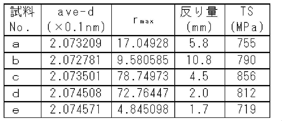
rmax<9.5・・・(3-1)
rmax≧20 ・・・(3-2)
rmax<9.5・・・(3-1)
rmax≧20 ・・・(3-2)
r=I111/I200・・(3-3)
但し、I111は、斜角入射X線回折法によって得られる、表面下1.45μmから7.11μmまでの{111}面の積分強度;
I200は、斜角入射X線回折法によって得られる、表面下1.45μmから7.11μmまでの{200}面の積分強度;
rmaxは、(3-3)式で定義される強度比rの最大値である。
次に、第4実施形態について詳述する。
I311/{I111+I200+I220+I311}≦0.08・・・(4-2)
0.93≦{I220+I200}/{I111+I200+I220+I311}・・・(4-3)
メタルマスク材料の{111}面、{220}面、{311}面及び{200}面の回折強度と、ハーフエッチング後の反り量との関係を以下の通り説明する。
r(1)=I200/{I111+I200+I220+I311}
r(2)=I311/{I111+I200+I220+I311}
r(3)={I220+I200}/{I111+I200+I220+I311}
また、表1のメタルマスク材料の試料No.a~eのそれぞれについて引張強度(TS)を測定した後、第1実施形態と同様にハーフエッチングを行い、反り量を測定した。その結果を表5に示す。

0.385≦r(1)=I200/{I111+I200+I220+I311}・・・(4-1)
r(2)=I311/{I111+I200+I220+I311}≦0.08・・・(4-2)
0.93≦r(3)={I220+I200}/{I111+I200+I220+I311}・・・(4-3)
次に、第5実施形態について詳述する。
メタルマスク材料の残留応力値の誤差σと、ハーフエッチング後の反り量との関係を以下の通り説明する。
R=Slope×K=Slope×{-E/(2×(1+ν))}×cotθ0×π/100・・・(5-2)

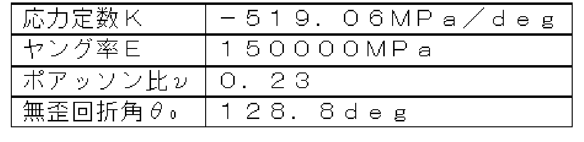

但し、α=211.1;β=5.355;γ=0.034886;上記式中のRは、集中法X線回折によって得られる残留応力値であり、σは前記集中法X線回折によって得られる残留応力値の誤差である。



次に、第6実施形態について詳述する。
メタルマスク材料の残留応力値の誤差σと、ハーフエッチング後の反り量との関係を以下の通り説明する。

0.02≦|c|・・・(6-2)
d/I≦12・・・(6-3)
2≧|e|/I・・・(6-4)
但し、I=(z×t3)/12
t:試料厚み(μm)
z:0.000768
b/I≦0.09・・・(6-1)
0.02≦|c|・・・(6-2)
d/I≦12・・・(6-3)
2≧|e|/I・・・(6-4)
2θ=a+b×sin2Ψ+c×sin(d×sin2Ψ+e)・・・(6-5)
但し、I=(z×t3)/12
t:板厚(μm)
z:0.000768
前述した第1実施形態~第6実施形態を含む本発明のメタルマスク材料は、オージェ電子分光法により測定された酸化皮膜厚が4.5nm以下であることが好ましい。ここで、「オージェ電子分光法により測定された酸化皮膜厚」とは、オージェ電子分光法によってメタルマスク材料の表面(深さ位置0)から深さ方向に検出された酸素濃度の最大値の1/2となる深さ位置をいう。表面からの深さは、スパッタリングレートとスパッタリング時間との積より換算して得られる。前記スパッタリングレートは、既知の酸化皮膜厚の標準試料であるシリコン熱酸化膜を用いて、使用するオージェ電子分光装置のイオン銃によるイオンスパッタリングを行い、酸素濃度が1/2となる時点をSiO2とSiとの界面に到達した時間とし、既知の酸化皮膜厚と前記界面に到達した時間から、算出されたものである。
本発明のメタルマスク材料及び本発明のメタルマスクの0.2%耐力は、330MPa以上850MPa以下であることが好ましい。なお、0.2%耐力は、常温での測定値である。0.2%耐力が330MPa未満では、エッチング工程や搬送の取り扱いによる皺や折れの発生により、生産性が低下する問題が起きる可能性がある。なお、鋼箔の0.2%耐力は、JIS Z2241に規定する金属材料引張試験方法に準拠する試験方法に基づいて測定される。試験片の形状は13B号、引張方向は圧延方向とする。鋼箔の皺や折れを防止する観点からは、特に、0.2%耐力の上限を限定する必要はない。しかしながら、取り扱いの容易性、及び工業的な圧延による加工硬化によって強度を得る際の安定性やエッチング後の反りとの相関を考慮すると、850MPaが鋼箔の0.2%耐力の実質的な上限となる。
また、本発明のメタルマスク材料は、圧延方向に対して直角方向の平均算術表面粗さRaが0.02μm以上0.10μm以下であることが好ましい。エッチング前にレジスト塗布を行う際、表面粗度が細かい方がレジストと材料の密着性が良くなり、非エッチング箇所へエッチング液が浸透し難くなる。そのため、エッチング後の部品寸法のバラつきを抑えることが可能になる。Ra:0.02μm以上0.10μm以下に調整するには、円周方向と直角方向のロール表面粗さRa:0.01μm以上0.30μm以下のロールを使用し、圧延速度を1.5m/s以上にて冷間圧延する等の方法を用いることができる。
本発明のメタルマスク材料の製造方法に関する実施形態を説明する。但し、その製造方法は以下に示す第7実施形態に係る製造方法に限定されることを意図しない。
まず、真空度が10-1(Torr)以下の真空雰囲気中で原料を溶解し、目的とするメタルマスク材料の組成の溶湯を得る。この時、Mn、Si、Mg、Al等の脱酸剤を加えて溶湯の清浄度を高めてからスラブに鋳造する。尚、スラブの鋳造工程は、前述した鋼組成を有するFe-Ni合金を電気炉で溶製し、前記溶湯を精錬した後、連続鋳造により、厚さが150mm~250mmのスラブを製造する工程としても良い。また、エレクトロスラグ再溶解(Electro-Slag-Remelting)或いは真空アーク再溶解(Vacuum electro-Slag-Remelting)にて、鋳造工程を行っても良い。
本発明のメタルマスク材料は、エッチングによる反り量が低減されるため、本発明に係るメタルマスク材料は精度の高いエッチングが可能であって、この材料を用いて製造されるメタルマスクは、高精細な解像度のOLEDの製造等に好適に使用できる。
本発明のメタルマスクの製造方法は、一般的な方法が適用でき、特に限定されるものではない。すなわち、本発明のメタルマスク材料の両面にレジストを形成した後、露光、現像する。その後、一方の面をウェットエッチングした後、レジストを除去し、エッチングされない保護層を形成する。その後、他方の面を上記と同様にウェットエッチングした後、レジストを除去することで、メタルマスク部が得られる。さらに、上記メタルマスク部に必要に応じてフレームを溶接することが可能である。レジストやエッチング液、保護層は一般的なものが適用できる。具体的には、レジストは、ドライフィルムの貼り付け、感光材の塗布等から選ばれる手法が使用できる。エッチング液は、塩化第二鉄液等の酸性溶液を浸漬またはスプレーする手法が適用できる。保護層は上記エッチング液に対する化学的耐性を有するものであればよい。
表10、11の条件にて、冷間圧延の圧下率と焼鈍温度を調整することにより、試料No.1~6のメタルマスク材料を製造した。表10に記載された元素成分は、試料No.1~6のメタルマスク材料の組成であり、表10の”CC”は連続鋳造によってスラブが製造されたことを示す。また、最終焼鈍は、水素ガス雰囲気化で4.0秒以上保定することにより行った。


ΔD=|DM-DL|・・・(1-2)
但し、DMは、斜角入射X線回折法によって得られる、表面下1.45μmから7.11μmまでの{111}面の平均格子面間隔(単位:nm)である。
ΔD≦0.00030・・・(1-1)
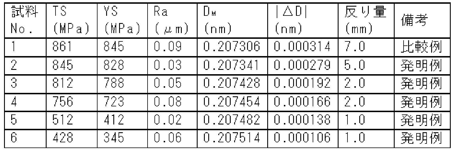
表10及び表11の試料No.1~6のそれぞれについて、斜角入射X線回折法を用いて表面下1.45μmから7.11μmまでの{111}面の平均半値幅(Hw111)を測定して、下記式X(Hwill,t)の値を求めた。また、試料No.1~6のそれぞれについて、引張強さ(TS)、降伏強度(YS)及びハーフエッチングの反り量を測定した。これらの測定結果を表13に示す。尚、表13の降伏強度(YS)は、JIS Z2241に規定する金属材料引張試験方法に準拠する試験方法に基づいて測定された0.2%耐力である。試料No.2~6は、ハーフエッチングの反り量が5.0mm以下であり、試料No.3~6は、表面下1.45μmから7.11μmまでの{111}面の平均半値幅が下記式(2-1)を満たしている。


表10及び表11の試料No.1~6のそれぞれについて、斜角入射X線回折法を用いて表面下1.45μmから7.11μmまでの{111}面の積分強度I111及び{200}面の積分強度I200を測定して、{200}面の積分強度I200に対する{111}面の積分強度I111の積分強度比r(=I111/I200)を求めた。前記積分強度比rのうち、最大値rmaxを表14に示す。また、試料No.1~6のそれぞれについて、引張強さ(TS)、降伏強度(YS)及びハーフエッチングの反り量を測定した。これらの測定結果を表14に示す。表14の降伏強度(YS)は、JIS Z2241に規定する金属材料引張試験方法に準拠する試験方法に基づいて測定された0.2%耐力である。
rmax<9.5・・・(3-1);rmax≧20・・・(3-2)

表10及び表11の試料No.1~6のそれぞれについて、集中法X線回折により{111}面、{200}面、{220}面、{311}面のそれぞれの回折強度を測定した。また、測定結果を用いて、前述した式で定義されるr(1)~r(3)のそれぞれの値を求めた。
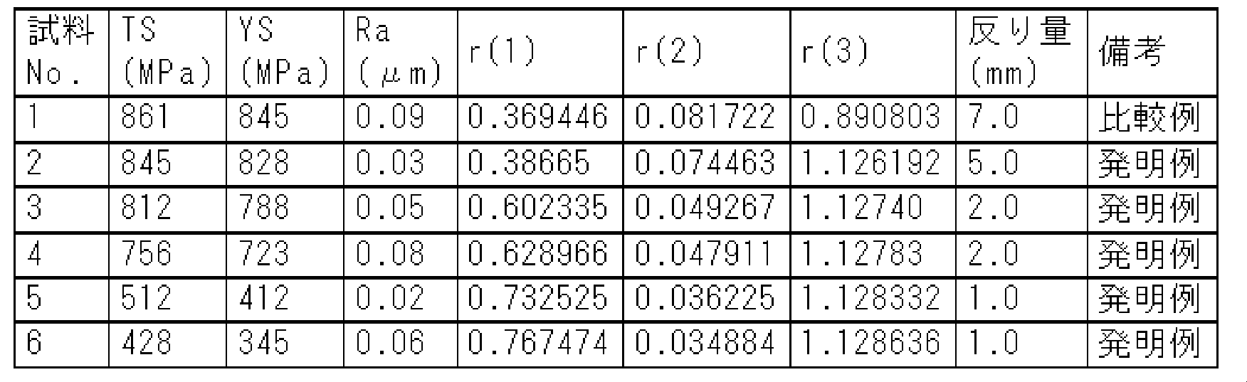
表10及び表11の試料No.1~6のそれぞれについて、表6の条件にて、集中法光学系のX線回折法を用いて、試料面の法線方向と{220}面法線との成す角度(Ψ(deg))と、前記角度Ψにおける{220}面の回折ピーク位置(2θ(deg))を測定した。次いで、縦軸を「2θ(deg)」の値とし、横軸を「sin2Ψ」の値とするグラフ上に、各Ψ角における{220}面の回折ピーク位置(2θ(deg))及び当該Ψ角におけるsin2Ψの値を座標としてプロットした。各Ψ角の全ての座標から最小二乗近似直線を求め、X線応力測定法(sin2Ψ法)を用いて残留応力値を測定した。また、前記最小二乗近似直線を用いた近似により生じる誤差を算出した。前記残留応力の測定値及び前記誤差を表16に示す。尚、残留応力値の算出に用いた各定数として、表7に示された値を用いた。
但し、α=211.1;β=5.355;γ=0.034886;上記式中のRは、集中法X線回折によって得られる残留応力値である。
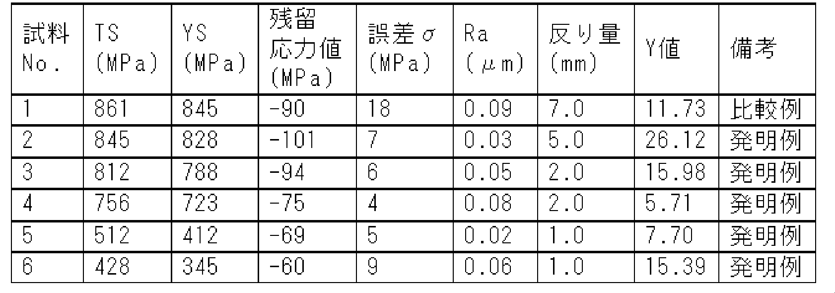
表10及び表11の試料No.1~6のそれぞれについて、表6の条件にて、集中法光学系のX線回折法を用いて、試料面の法線方向と{220}面法線との成す角度(Ψ(deg))と、前記角度Ψにおける{220}面の回折ピーク位置(2θ(deg))を測定した。次いで、縦軸を「2θ(deg)」の値とし、横軸を「sin2Ψ」の値とするグラフ上に、各Ψ角における{220}面の回折ピーク位置(2θ(deg))及び当該Ψ角におけるsin2Ψの値を座標としてプロットした。各Ψ角の全ての座標から最小二乗近似直線を求め、X線応力測定法(sin2Ψ法)を用いて残留応力値を測定した。

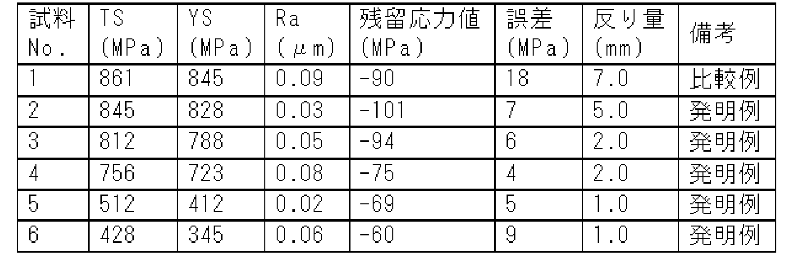
1a・・・マスク孔
2・・・基板
3・・・有機EL発光材料の蒸着源
3a・・・有機EL発光材料
Claims (14)
- 質量%にて、Ni:35.0~37.0%、Co:0.00~0.50%を含有し、残部がFe及び不純物からなり、
板厚が5.00μm以上50.00μm以下であるメタルマスク材料であって、
一辺が100mmの正方形の前記メタルマスク材料の試料を、当該試料の板厚が2/5になるまでその片側からエッチングをし、エッチングをした前記試料を定盤に載置した時の、前記試料の4角の浮き上がり量のうち最大値である反り量が5.0mm以下であることを特徴とするメタルマスク材料。 - 更に、質量%にて、C:0.05%以下、Ca:0.0005%以下を含有することを特徴とする、請求項1に記載のメタルマスク材料。
- 前記不純物は、Si:0.30%以下、Mn:0.70%以下、Al:0.01%以下、Mg:0.0005%以下、P:0.030%以下、S:0.015%以下に制限されることを特徴とする、請求項1又は2に記載のメタルマスク材料。
- 表面下1.45μmから7.11μmまでの{111}面の平均格子面間隔が下記(1-1)式および(1-2)式を満足することを特徴とする、請求項1~3のうちいずれか1項に記載のメタルマスク材料。
ΔD≦0.00030・・・(1-1)
ΔD=|DM-DL|・・・(1-2)
但し、上記式中のDM及びDLの定義は、下記の通りである。
DM:斜角入射X線回折法によって得られる{111}面の平均格子面間隔(単位:nm);
DL:{111}面の格子面間隔の基準値(単位:nm)又はバルクの平均の格子定数から算出される{111}面の平均格子面間隔(単位:nm) - 下記(2-1)式を満足することを特徴とする、請求項1~3のうちいずれか1項に記載のメタルマスク材料。

- 下記(3-1)式又は(3-2)式のいずれかを満足することを特徴とする、請求項1~3のうちいずれか1項に記載のメタルマスク材料。
rmax<9.5・・・(3-1)
rmax≧20 ・・・(3-2)
r=I111/I200・・(3-3)
但し、I111は、斜角入射X線回折法によって得られる、表面下1.45μmから7.11μmまでの{111}面の積分強度;
I200は、斜角入射X線回折法によって得られる、表面下1.45μmから7.11μmまでの{200}面の積分強度;
rmaxは、(3-3)式で定義される積分強度比の最大値である。 - 下記(4-1)式~(4-3)式を満足することを特徴とする、請求項1~3のうちいずれか1項に記載のメタルマスク材料。
0.385≦I200/{I111+I200+I220+I311}・・・(4-1)
I311/{I111+I200+I220+I311}≦0.08・・・(4-2)
0.93≦{I220+I200}/{I111+I200+I220+I311}・・・(4-3)
但し、上記式中のI200は、集中法X線回折によって得られる{200}面の回折強度であり、I111は{111}面の回折強度であり、I220は{220}面の回折強度であり、I311は前記{311}面の回折強度である。 - X線応力測定法を用いて残留応力を測定した際に算出される誤差が、下記(5-1)式を満足することを特徴とする、請求項1~3のうちいずれか1項に記載のメタルマスク材料。
σ≦α+β×R+γ×R2・・・(5-1)
但し、α=211.1;β=5.355;γ=0.034886;上記式中のRは、前記X線応力測定法を用いて測定された残留応力値であり、σは前記X線応力測定法を用いて残留応力値を測定した際に算出される誤差である。 - X線応力測定法を用いて応力を測定した時に、前記メタルマスク材料の面法線と{220}面法線との成す角度(Ψ(deg))と、前記角度Ψにおける{220}面の回折ピーク位置(2θ(deg))との関係が下記(6-5)式で表され、且つ前記(6-5)式の係数であるb、c、d、eが下記(6-1)式~(6-4)式を満たすことを特徴とする、請求項1~3のうちいずれか1項に記載のメタルマスク材料。
b/I≦0.09・・・(6-1)
0.02≦|c|・・・(6-2)
d/I≦12・・・(6-3)
2≧|e|/I・・・(6-4)
2θ=a+b×sin2Ψ+c×sin(d×sin2Ψ+e)・・・(6-5)
但し、I=(z×t3)/12
t:板厚(μm)
z:0.000768 - オージェ電子分光法により測定された酸化皮膜厚が4.5nm以下であることを特徴とする、請求項4~9のうちいずれか1項に記載のメタルマスク材料。
- 0.2%耐力が330MPa以上850MPa以下であることを特徴とする、請求項4~10のうちいずれか1項に記載のメタルマスク材料。
- 圧延方向と直角方向の平均算術表面粗さRaが0.02μm以上0.10μm以下であることを特徴とする、請求項4~11のうちいずれか1項に記載のメタルマスク材料。
- 請求項1~3のうちいずれか1項に記載の組成を有する合金を溶製する工程と、
前記溶製された合金から鋼片を得る工程と、
前記鋼片を熱間圧延して巻取ることにより熱間圧延板を得る巻取工程と、
前記巻取工程後に前記熱間圧延板に対して冷間圧延と焼鈍とを少なくとも1回ずつ交互に行うことによって板厚5.00~50.00μmの鋼箔を得る工程と、
テンションアニール工程とを含み、
前記テンションアニール工程は最終圧延工程後に行われ、最終圧延工程での圧下率は30.0%以上95.0%以下であって、前記テンションアニール工程は焼鈍温度が300~900℃であって、還元雰囲気で行われることを特徴とする、請求項1~12のうちいずれか1項に記載のメタルマスク材料の製造方法。 - 請求項1~12のうちいずれか1項のメタルマスク材料を用いたことを特徴とする、メタルマスク。
Priority Applications (5)
| Application Number | Priority Date | Filing Date | Title |
|---|---|---|---|
| EP19866278.5A EP3859029A4 (en) | 2018-09-27 | 2019-09-27 | METAL MASK MATERIAL, METHOD FOR ITS PRODUCTION AND METAL MASK |
| JP2019559127A JP6704540B1 (ja) | 2018-09-27 | 2019-09-27 | メタルマスク材料及びその製造方法とメタルマスク |
| CN201980063786.2A CN112752860A (zh) | 2018-09-27 | 2019-09-27 | 金属掩膜材料及其制造方法、金属掩膜 |
| US17/280,765 US12037673B2 (en) | 2018-09-27 | 2019-09-27 | Metal mask material, method for manufacturing same, and metal mask |
| KR1020217009057A KR102684761B1 (ko) | 2018-09-27 | 2019-09-27 | 메탈 마스크 재료 및 그의 제조 방법과 메탈 마스크 |
Applications Claiming Priority (12)
| Application Number | Priority Date | Filing Date | Title |
|---|---|---|---|
| JP2018183001 | 2018-09-27 | ||
| JP2018183002 | 2018-09-27 | ||
| JP2018183007 | 2018-09-27 | ||
| JP2018-182992 | 2018-09-27 | ||
| JP2018-183001 | 2018-09-27 | ||
| JP2018182993 | 2018-09-27 | ||
| JP2018-183007 | 2018-09-27 | ||
| JP2018182992 | 2018-09-27 | ||
| JP2018183006 | 2018-09-27 | ||
| JP2018-182993 | 2018-09-27 | ||
| JP2018-183006 | 2018-09-27 | ||
| JP2018-183002 | 2018-09-27 |
Publications (2)
| Publication Number | Publication Date |
|---|---|
| WO2020067537A1 true WO2020067537A1 (ja) | 2020-04-02 |
| WO2020067537A9 WO2020067537A9 (ja) | 2020-08-20 |
Family
ID=69951964
Family Applications (1)
| Application Number | Title | Priority Date | Filing Date |
|---|---|---|---|
| PCT/JP2019/038416 Ceased WO2020067537A1 (ja) | 2018-09-27 | 2019-09-27 | メタルマスク材料及びその製造方法とメタルマスク |
Country Status (7)
| Country | Link |
|---|---|
| US (1) | US12037673B2 (ja) |
| EP (1) | EP3859029A4 (ja) |
| JP (1) | JP6704540B1 (ja) |
| KR (1) | KR102684761B1 (ja) |
| CN (1) | CN112752860A (ja) |
| TW (1) | TWI805853B (ja) |
| WO (1) | WO2020067537A1 (ja) |
Cited By (4)
| Publication number | Priority date | Publication date | Assignee | Title |
|---|---|---|---|---|
| CN115369355A (zh) * | 2022-10-25 | 2022-11-22 | 浙江众凌科技有限公司 | 一种用于oled像素沉积的金属掩膜版及加工方法 |
| WO2024004613A1 (ja) * | 2022-06-30 | 2024-01-04 | 日鉄ケミカル&マテリアル株式会社 | Fe-Ni合金箔、Fe-Ni合金箔の製造方法、および部品 |
| WO2024143061A1 (ja) * | 2022-12-28 | 2024-07-04 | Toppanホールディングス株式会社 | メタルマスク用基材、メタルマスク、および、メタルマスクの製造方法 |
| JP2026052793A (ja) * | 2024-09-12 | 2026-03-25 | Toppanホールディングス株式会社 | メタルマスク、およびメタルマスクの製造方法 |
Families Citing this family (3)
| Publication number | Priority date | Publication date | Assignee | Title |
|---|---|---|---|---|
| KR102854300B1 (ko) * | 2022-01-11 | 2025-09-05 | 주식회사 오럼머티리얼 | 마스크의 인장력 제어 방법 및 프레임 일체형 마스크의 제조 방법 |
| JP2023111881A (ja) * | 2022-01-31 | 2023-08-10 | 大日本印刷株式会社 | マスクの検査方法、マスクの製造方法、マスクの検査装置、プログラム、記録媒体及びマスク |
| WO2023191594A1 (ko) * | 2022-03-31 | 2023-10-05 | 스템코 주식회사 | 금속판과 이를 활용한 증착 마스크 및 그 제조 방법 |
Citations (11)
| Publication number | Priority date | Publication date | Assignee | Title |
|---|---|---|---|---|
| WO2000070108A1 (fr) | 1999-05-12 | 2000-11-23 | Toyo Kohan Co., Ltd. | Materiau pour masque perfore, masque perfore et tube de reception d'images couleurs comportant ce masque perfore |
| JP2003027188A (ja) | 2001-07-19 | 2003-01-29 | Sumitomo Metal Ind Ltd | シャド−マスク用インバ−合金とその製造法 |
| JP2004115905A (ja) | 2002-09-30 | 2004-04-15 | Hitachi Metals Ltd | 低熱膨張合金及び低熱膨張合金板 |
| JP2004183023A (ja) | 2002-12-02 | 2004-07-02 | Hitachi Metals Ltd | メタルマスク |
| JP2010214447A (ja) * | 2009-03-18 | 2010-09-30 | Hitachi Metals Ltd | エッチング加工用素材の製造方法及びエッチング加工用素材 |
| JP2014101543A (ja) | 2012-11-20 | 2014-06-05 | Jx Nippon Mining & Metals Corp | メタルマスク材料及びメタルマスク |
| JP2015078401A (ja) | 2013-10-15 | 2015-04-23 | 大日本印刷株式会社 | 金属板、金属板の製造方法、および金属板を用いて蒸着マスクを製造する方法 |
| JP2017088915A (ja) | 2015-11-04 | 2017-05-25 | Jx金属株式会社 | メタルマスク材料及びメタルマスク |
| JP2017088914A (ja) * | 2015-11-04 | 2017-05-25 | Jx金属株式会社 | メタルマスク材料及びメタルマスク |
| WO2018043642A1 (ja) * | 2016-08-31 | 2018-03-08 | 日立金属株式会社 | メタルマスク用素材およびその製造方法 |
| WO2018043641A1 (ja) | 2016-08-31 | 2018-03-08 | 日立金属株式会社 | メタルマスク用素材およびその製造方法 |
Family Cites Families (14)
| Publication number | Priority date | Publication date | Assignee | Title |
|---|---|---|---|---|
| JP2590657B2 (ja) | 1991-12-12 | 1997-03-12 | 日本鋼管株式会社 | 焼鈍時の密着焼付防止性およびガス放散性に優れたFe−Ni合金およびその製造方法 |
| JPH0762495A (ja) | 1993-08-20 | 1995-03-07 | Nkk Corp | エッチング加工性に優れた電子機器用合金薄板 |
| US5308723A (en) * | 1992-01-24 | 1994-05-03 | Nkk Corporation | Thin metallic sheet for shadow mask |
| US5605582A (en) * | 1992-01-24 | 1997-02-25 | Nkk Corporation | Alloy sheet having high etching performance |
| KR100244233B1 (en) * | 1997-12-03 | 2000-02-01 | Lg Electronics Inc | Shadow mask for cathode ray tube and method of manufacturing thereof |
| KR100244232B1 (en) * | 1997-12-03 | 2000-02-01 | Lg Electronics Inc | Shadow mask for cathode ray tube and method of manufacturing thereof |
| KR100523430B1 (ko) * | 2002-08-23 | 2005-10-25 | 닛꼬 긴조꾸 가꼬 가부시키가이샤 | 에칭 후의 형상이 양호한 섀도우 마스크용 연강조 및철-니켈계 합금조 |
| US20040261911A1 (en) * | 2003-06-30 | 2004-12-30 | Yuko Kondo | Strip material used for shadow mask having improved post-etching shape |
| DE102006005250B4 (de) * | 2006-02-02 | 2010-04-29 | Thyssenkrupp Vdm Gmbh | Eisen-Nickel-Legierung |
| JP5382257B1 (ja) * | 2013-01-10 | 2014-01-08 | 大日本印刷株式会社 | 金属板、金属板の製造方法、および金属板を用いて蒸着マスクを製造する方法 |
| JP6356029B2 (ja) * | 2014-09-25 | 2018-07-11 | 東京エレクトロン株式会社 | メタルハードマスクおよびその製造方法 |
| CN105803333A (zh) * | 2015-01-20 | 2016-07-27 | 日立金属株式会社 | Fe-Ni系合金薄板的制造方法 |
| KR102509663B1 (ko) * | 2015-07-17 | 2023-03-14 | 도판 인사츠 가부시키가이샤 | 메탈 마스크용 기재의 제조 방법, 증착용 메탈 마스크의 제조 방법, 메탈 마스크용 기재, 및, 증착용 메탈 마스크 |
| JP6998139B2 (ja) * | 2017-06-28 | 2022-01-18 | 株式会社ジャパンディスプレイ | 蒸着マスク |
-
2019
- 2019-09-27 US US17/280,765 patent/US12037673B2/en active Active
- 2019-09-27 EP EP19866278.5A patent/EP3859029A4/en active Pending
- 2019-09-27 CN CN201980063786.2A patent/CN112752860A/zh active Pending
- 2019-09-27 JP JP2019559127A patent/JP6704540B1/ja active Active
- 2019-09-27 TW TW108135338A patent/TWI805853B/zh active
- 2019-09-27 WO PCT/JP2019/038416 patent/WO2020067537A1/ja not_active Ceased
- 2019-09-27 KR KR1020217009057A patent/KR102684761B1/ko active Active
Patent Citations (11)
| Publication number | Priority date | Publication date | Assignee | Title |
|---|---|---|---|---|
| WO2000070108A1 (fr) | 1999-05-12 | 2000-11-23 | Toyo Kohan Co., Ltd. | Materiau pour masque perfore, masque perfore et tube de reception d'images couleurs comportant ce masque perfore |
| JP2003027188A (ja) | 2001-07-19 | 2003-01-29 | Sumitomo Metal Ind Ltd | シャド−マスク用インバ−合金とその製造法 |
| JP2004115905A (ja) | 2002-09-30 | 2004-04-15 | Hitachi Metals Ltd | 低熱膨張合金及び低熱膨張合金板 |
| JP2004183023A (ja) | 2002-12-02 | 2004-07-02 | Hitachi Metals Ltd | メタルマスク |
| JP2010214447A (ja) * | 2009-03-18 | 2010-09-30 | Hitachi Metals Ltd | エッチング加工用素材の製造方法及びエッチング加工用素材 |
| JP2014101543A (ja) | 2012-11-20 | 2014-06-05 | Jx Nippon Mining & Metals Corp | メタルマスク材料及びメタルマスク |
| JP2015078401A (ja) | 2013-10-15 | 2015-04-23 | 大日本印刷株式会社 | 金属板、金属板の製造方法、および金属板を用いて蒸着マスクを製造する方法 |
| JP2017088915A (ja) | 2015-11-04 | 2017-05-25 | Jx金属株式会社 | メタルマスク材料及びメタルマスク |
| JP2017088914A (ja) * | 2015-11-04 | 2017-05-25 | Jx金属株式会社 | メタルマスク材料及びメタルマスク |
| WO2018043642A1 (ja) * | 2016-08-31 | 2018-03-08 | 日立金属株式会社 | メタルマスク用素材およびその製造方法 |
| WO2018043641A1 (ja) | 2016-08-31 | 2018-03-08 | 日立金属株式会社 | メタルマスク用素材およびその製造方法 |
Non-Patent Citations (3)
| Title |
|---|
| "Iron and Steel Handbook", article "X-Ray Diffraction Analysis" |
| "Iron and Steel", 2002, SOCIETY OF MATERIAL SCIENCES JAPAN, article "Standard for X-Ray Stress Measurement", pages: 81 |
| ONO, F.KITTAKA, T.MAETA, H., PHYSICA B+C, vol. 119, pages 78 - 83 |
Cited By (5)
| Publication number | Priority date | Publication date | Assignee | Title |
|---|---|---|---|---|
| WO2024004613A1 (ja) * | 2022-06-30 | 2024-01-04 | 日鉄ケミカル&マテリアル株式会社 | Fe-Ni合金箔、Fe-Ni合金箔の製造方法、および部品 |
| EP4545664A4 (en) * | 2022-06-30 | 2025-10-22 | Nippon Steel Chemical & Mat Co Ltd | IRON-NICKEL ALLOY SHEET, METHOD FOR MANUFACTURING IRON-NICKEL ALLOY SHEET, AND COMPONENT |
| CN115369355A (zh) * | 2022-10-25 | 2022-11-22 | 浙江众凌科技有限公司 | 一种用于oled像素沉积的金属掩膜版及加工方法 |
| WO2024143061A1 (ja) * | 2022-12-28 | 2024-07-04 | Toppanホールディングス株式会社 | メタルマスク用基材、メタルマスク、および、メタルマスクの製造方法 |
| JP2026052793A (ja) * | 2024-09-12 | 2026-03-25 | Toppanホールディングス株式会社 | メタルマスク、およびメタルマスクの製造方法 |
Also Published As
| Publication number | Publication date |
|---|---|
| TWI805853B (zh) | 2023-06-21 |
| EP3859029A1 (en) | 2021-08-04 |
| KR20210049888A (ko) | 2021-05-06 |
| US20210340664A1 (en) | 2021-11-04 |
| US12037673B2 (en) | 2024-07-16 |
| KR102684761B1 (ko) | 2024-07-15 |
| EP3859029A4 (en) | 2022-11-02 |
| JP6704540B1 (ja) | 2020-06-03 |
| CN112752860A (zh) | 2021-05-04 |
| TW202031913A (zh) | 2020-09-01 |
| WO2020067537A9 (ja) | 2020-08-20 |
| JPWO2020067537A1 (ja) | 2021-02-15 |
Similar Documents
| Publication | Publication Date | Title |
|---|---|---|
| JP6704540B1 (ja) | メタルマスク材料及びその製造方法とメタルマスク | |
| JPWO2018043642A1 (ja) | メタルマスク用素材およびその製造方法 | |
| US6229255B1 (en) | Shadow mask in color CRT having specific materials | |
| JP6807038B2 (ja) | メタルマスク用素材およびその製造方法 | |
| CN100354446C (zh) | 用于制造荫罩的具有较低热膨胀系数的铁镍合金 | |
| WO1998051833A1 (fr) | Materiau de type tole d'acier en alliage invar pour masque perfore, procede de production de ce materiau, masque perfore, et tube d'images couleur | |
| JP2011012334A (ja) | フォトエッチング加工用ステンレス鋼板およびその製造方法 | |
| KR100595393B1 (ko) | 내식성이 우수한 섀도우 마스크 소재용 FeNi계 합금및 섀도우 마스크 재료 | |
| US6316869B1 (en) | Shadow mask in color CRT | |
| JP3288656B2 (ja) | Fe−Ni系シャドウマスク用材料 | |
| CN1219902C (zh) | 蚀刻后的形状良好的荫罩条材 | |
| JP2001152292A (ja) | 磁気特性に優れたセミテンションマスク用Fe−Ni系合金並びにそれを用いたセミテンションマスク及びカラーブラウン管 | |
| JP2523603B2 (ja) | 高精細度シヤドウマスク | |
| JP2795028B2 (ja) | エッチング加工性に優れたシャドウマスク用金属薄板 | |
| TW200303928A (en) | Low thermal expansion alloy sheet and method for manufacturing the same | |
| JP3623620B2 (ja) | シャドウマスク用素材のエッチング性評価方法及びエッチング後にスジむらが発生しないシャドウマスク用素材 | |
| JP3288655B2 (ja) | Fe−Ni系シャドウマスク用材料 | |
| Kempf et al. | Relationships between strain, microstructure and oxide growth at the nano‐and microscale | |
| JP3309680B2 (ja) | エッチング性に優れた電子部品用低熱膨張合金薄板 | |
| JP3309679B2 (ja) | エッチング性に優れた電子部品用低熱膨張合金薄板 | |
| JPH07268558A (ja) | シャドウマスク用オーステナイトFe−Ni系合金原板およびその製造方法 | |
| JP2003003244A (ja) | フォトエッチング加工用ステンレス鋼板およびその製造方法 | |
| JPH05311358A (ja) | シャドウマスク材 | |
| JP2000219913A (ja) | エッチング性に優れた電子部品用低熱膨張合金の分塊圧延方法 | |
| CN1318651A (zh) | 荫罩用Fe-Ni合金和杂质观察法和电子线透过孔均匀性判别法 |
Legal Events
| Date | Code | Title | Description |
|---|---|---|---|
| ENP | Entry into the national phase |
Ref document number: 2019559127 Country of ref document: JP Kind code of ref document: A |
|
| 121 | Ep: the epo has been informed by wipo that ep was designated in this application |
Ref document number: 19866278 Country of ref document: EP Kind code of ref document: A1 |
|
| ENP | Entry into the national phase |
Ref document number: 20217009057 Country of ref document: KR Kind code of ref document: A |
|
| NENP | Non-entry into the national phase |
Ref country code: DE |
|
| ENP | Entry into the national phase |
Ref document number: 2019866278 Country of ref document: EP Effective date: 20210428 |