WO2020021772A1 - スパッタリングターゲット及びスパッタリングターゲットの製造方法 - Google Patents
スパッタリングターゲット及びスパッタリングターゲットの製造方法 Download PDFInfo
- Publication number
- WO2020021772A1 WO2020021772A1 PCT/JP2019/013572 JP2019013572W WO2020021772A1 WO 2020021772 A1 WO2020021772 A1 WO 2020021772A1 JP 2019013572 W JP2019013572 W JP 2019013572W WO 2020021772 A1 WO2020021772 A1 WO 2020021772A1
- Authority
- WO
- WIPO (PCT)
- Prior art keywords
- plane
- target
- sputtering
- cobalt
- sputtering target
- Prior art date
- Legal status (The legal status is an assumption and is not a legal conclusion. Google has not performed a legal analysis and makes no representation as to the accuracy of the status listed.)
- Ceased
Links
Images


Classifications
-
- C—CHEMISTRY; METALLURGY
- C22—METALLURGY; FERROUS OR NON-FERROUS ALLOYS; TREATMENT OF ALLOYS OR NON-FERROUS METALS
- C22C—ALLOYS
- C22C19/00—Alloys based on nickel or cobalt
- C22C19/07—Alloys based on nickel or cobalt based on cobalt
-
- B—PERFORMING OPERATIONS; TRANSPORTING
- B21—MECHANICAL METAL-WORKING WITHOUT ESSENTIALLY REMOVING MATERIAL; PUNCHING METAL
- B21B—ROLLING OF METAL
- B21B37/00—Control devices or methods specially adapted for metal-rolling mills or the work produced thereby
- B21B37/16—Control of thickness, width, diameter or other transverse dimensions
-
- B—PERFORMING OPERATIONS; TRANSPORTING
- B21—MECHANICAL METAL-WORKING WITHOUT ESSENTIALLY REMOVING MATERIAL; PUNCHING METAL
- B21B—ROLLING OF METAL
- B21B45/00—Devices for surface or other treatment of work, specially combined with or arranged in, or specially adapted for use in connection with, metal-rolling mills
- B21B45/004—Heating the product
-
- C—CHEMISTRY; METALLURGY
- C22—METALLURGY; FERROUS OR NON-FERROUS ALLOYS; TREATMENT OF ALLOYS OR NON-FERROUS METALS
- C22F—CHANGING THE PHYSICAL STRUCTURE OF NON-FERROUS METALS AND NON-FERROUS ALLOYS
- C22F1/00—Changing the physical structure of non-ferrous metals or alloys by heat treatment or by hot or cold working
- C22F1/10—Changing the physical structure of non-ferrous metals or alloys by heat treatment or by hot or cold working of nickel or cobalt or alloys based thereon
-
- C—CHEMISTRY; METALLURGY
- C23—COATING METALLIC MATERIAL; COATING MATERIAL WITH METALLIC MATERIAL; CHEMICAL SURFACE TREATMENT; DIFFUSION TREATMENT OF METALLIC MATERIAL; COATING BY VACUUM EVAPORATION, BY SPUTTERING, BY ION IMPLANTATION OR BY CHEMICAL VAPOUR DEPOSITION, IN GENERAL; INHIBITING CORROSION OF METALLIC MATERIAL OR INCRUSTATION IN GENERAL
- C23C—COATING METALLIC MATERIAL; COATING MATERIAL WITH METALLIC MATERIAL; SURFACE TREATMENT OF METALLIC MATERIAL BY DIFFUSION INTO THE SURFACE, BY CHEMICAL CONVERSION OR SUBSTITUTION; COATING BY VACUUM EVAPORATION, BY SPUTTERING, BY ION IMPLANTATION OR BY CHEMICAL VAPOUR DEPOSITION, IN GENERAL
- C23C14/00—Coating by vacuum evaporation, by sputtering or by ion implantation of the coating forming material
- C23C14/22—Coating by vacuum evaporation, by sputtering or by ion implantation of the coating forming material characterised by the process of coating
- C23C14/34—Sputtering
- C23C14/3407—Cathode assembly for sputtering apparatus, e.g. Target
- C23C14/3414—Metallurgical or chemical aspects of target preparation, e.g. casting, powder metallurgy
-
- H—ELECTRICITY
- H01—ELECTRIC ELEMENTS
- H01F—MAGNETS; INDUCTANCES; TRANSFORMERS; SELECTION OF MATERIALS FOR THEIR MAGNETIC PROPERTIES
- H01F41/00—Apparatus or processes specially adapted for manufacturing or assembling magnets, inductances or transformers; Apparatus or processes specially adapted for manufacturing materials characterised by their magnetic properties
- H01F41/14—Apparatus or processes specially adapted for manufacturing or assembling magnets, inductances or transformers; Apparatus or processes specially adapted for manufacturing materials characterised by their magnetic properties for applying magnetic films to substrates
- H01F41/18—Apparatus or processes specially adapted for manufacturing or assembling magnets, inductances or transformers; Apparatus or processes specially adapted for manufacturing materials characterised by their magnetic properties for applying magnetic films to substrates by cathode sputtering
- H01F41/183—Sputtering targets therefor
-
- C—CHEMISTRY; METALLURGY
- C22—METALLURGY; FERROUS OR NON-FERROUS ALLOYS; TREATMENT OF ALLOYS OR NON-FERROUS METALS
- C22F—CHANGING THE PHYSICAL STRUCTURE OF NON-FERROUS METALS AND NON-FERROUS ALLOYS
- C22F1/00—Changing the physical structure of non-ferrous metals or alloys by heat treatment or by hot or cold working
Definitions
- the present invention relates to a sputtering target and a method for manufacturing a sputtering target.
- a method for forming a thin film material used for a device such as a semiconductor device there is a sputtering method.
- the magnetron sputtering method in which the film forming speed is improved is often used.
- target magnetron sputtering method sputtering target
- problems For example, when the magnetic field leaking from the magnet disposed on the back surface of the target to the target surface is weak, the magnetic flux density on the target surface is reduced, and the sputtering efficiency is significantly reduced.
- Patent Document 1 there is a technique for improving the sputtering efficiency of a cobalt target by reducing the magnetic permeability in a direction parallel to the sputtering surface and increasing the magnetic permeability in a direction perpendicular to the sputtering surface (for example, Patent Document 1). reference).
- an object of the present invention is to provide a sputtering target and a method for manufacturing a sputtering target with further improved sputtering efficiency.
- a sputtering target is a cobalt target having a sputtering surface and a purity of 99.95 wt% or more.
- Plane intensity ratio (I (002) + I (004) ) / (I (100) + I (002) + I (101) + I (102) + I (110) + I (103) + I ( 112) + I (004) ) is 0.85 or more.
- the amount of the axis of easy magnetization C oriented perpendicular to the sputtering surface of the cobalt target is extremely high, so that the effect of trapping plasma near the sputtering surface is enhanced and the sputtering efficiency is greatly improved. Furthermore, since the direction of the axis of easy magnetization C is uniformly aligned on the sputtering surface, a film having a uniform film thickness distribution and a film having a uniform sheet resistance are formed on the substrate by using the target.
- the relative magnetic permeability along the sputtering surface may be less than 5.
- the relative magnetic permeability along the sputtering surface is less than 5
- the magnetic flux density leaking perpendicular to the sputtering surface is extremely high.
- the effect of trapping plasma near the sputtering surface is enhanced, and the sputtering efficiency is greatly improved.
- a film having a uniform film thickness distribution and a film having a uniform sheet resistance are formed on the substrate.
- the half value width of the X-ray diffraction peak corresponding to the (002) plane of the hexagonal close-packed lattice structure along the sputtering surface may be 0.3 ° or less.
- the half value width of the X-ray diffraction peak corresponding to the (002) plane of the hexagonal close-packed lattice structure along the sputtering plane is 0.3 ° or less, the axis of easy magnetization C This means that the directions are uniformly aligned on the sputtering surface. Thereby, the effect of trapping plasma near the sputtering surface is enhanced, and the sputtering efficiency is greatly improved. Further, when the target is used, a film having a uniform film thickness distribution and a film having a uniform sheet resistance are formed on the substrate.
- a cobalt ingot is subjected to hot forging and hot rolling to form a cobalt plate.
- the first vacuum heating is performed on the cobalt plate at a temperature higher than a transition temperature at which a transition from a hexagonal close-packed lattice structure to a face-centered cubic structure is made.
- the cobalt plate is vacuum cooled so that the temperature of the cobalt plate is lower than the transition temperature.
- Cold rolling is performed on the cobalt sheet so that the rolling reduction is 17% or more and 35% or less.
- the second vacuum heating is performed on the cobalt plate at a temperature lower than the transition temperature.
- the amount of the axis of easy magnetization C oriented perpendicular to the sputtering surface of the cobalt target is significantly increased, so that the effect of trapping plasma near the sputtering surface is enhanced, and the sputtering efficiency is reduced. Greatly improved. Furthermore, since the direction of the axis of easy magnetization C is uniformly aligned on the sputtering surface, a film having a uniform film thickness distribution and a film having a uniform sheet resistance are formed on the substrate by using the target.
- a sputtering target with further improved sputtering efficiency and a method for manufacturing a sputtering target are provided.
- FIG. 1A is a schematic perspective view of a target according to the present embodiment.
- FIG. 2B is a schematic perspective view of the target according to the reference example. It is a flowchart which shows the manufacturing process of the target which concerns on this embodiment.
- FIG. 3 is a schematic diagram illustrating a process of manufacturing a target corresponding to FIG. 2.
- 5 is an X-ray diffraction measurement result of the target according to the embodiment. It is a graph which shows the ratio of the peak intensity of XRD.
- FIG. 1A is a schematic perspective view of the target according to the present embodiment.
- FIG. 1B is a schematic perspective view of a target according to a reference example.
- the target 100 according to the present embodiment shown in FIG. 1A is a sputtering target having a purity of cobalt of 99.95 wt% or more, for example, a purity of cobalt of 5N (99.999) wt% or more.
- FIG. 1A shows a disk-shaped target 100 as an example.
- the XY axis plane corresponds to a plane parallel to the sputtering surface 10a and the back surface 10b of the target 100.
- the Z axis corresponds to the thickness direction of the target 100.
- the target 100 has a sputtering surface 10a and a back surface 10b opposite to the sputtering surface 10a.
- the sputtering surface 10a is a surface that is exposed to plasma (sputtering gas) during sputtering film formation.
- the back surface 10b is a surface facing a magnet (not shown). That is, a magnet is arranged on the side of the back surface 10b, and the target 100 is used as a target for magnetron sputtering. If necessary, a backing plate may be provided on the back surface 10b side.
- the outer shape of the target 100 is 100 mm or more and 500 mm or less, for example, 400 mm.
- the target 100 is not limited to a disk shape but may be a rectangular plate.
- the horizontal length is 250 mm or more and 500 mm or less
- the vertical length is 100 mm or more and 150 mm or less.
- the thickness of the target 100 is 2 mm or more and 6 mm or less, for example, 3 mm.
- the target 100 is formed of a hexagonal close-packed lattice structure (hcp) of cobalt, and its easy axis of magnetization C is preferentially oriented perpendicular to the sputtering surface 10a of the target 100.
- hcp hexagonal close-packed lattice structure
- the magnetic flux B leaking from the magnet arranged on the back surface 10b side of the target 100 to the sputtering surface 10a via the inside of the target 100 increases, and the magnetic flux density near the sputtering surface 10a decreases. Get higher.
- the target 100 has uniform magnetic characteristics.
- a film having a uniform film thickness distribution and a film having a uniform sheet resistance are formed on the substrate.
- the axis of easy magnetization C of the hexagonal close-packed lattice structure of cobalt is obliquely inclined with respect to the sputtering surface 10a, or oriented in parallel, or If a face-centered cubic (fcc) crystal of cobalt remains, magnetic flux from a magnet easily enters the inside of the target 101, and the magnetic flux density near the sputtering surface 10a decreases. Alternatively, the variation in the magnetic flux density near the sputtering surface 10a may increase.
- the (002) plane and the (004) plane of the hexagonal close-packed lattice structure are the sputtering planes in the entire area of the sputtering plane 10a. It is oriented along 10a.
- the hcp (002) plane and the hcp (004) are planes perpendicular to the easy axis C.
- the (100), (002), (101), (102), (110), (103), and (103) planes of the hexagonal close-packed lattice structure along the sputtering surface 10a Intensity ratio of X-ray diffraction peaks corresponding to (112) plane and (004) plane (I (002) + I (004) ) / (I (100) + I (002) + I (101) + I (102) + I (110 ) ) + I (103) + I (112) + I (004) ) is 0.85 or more as an average value of a plurality of points measured on the sputtering surface 10a. In this intensity ratio, 0.9 or more is more preferable, and 0.95 or more is still more preferable. If the above intensity ratio is less than 0.85, a sufficiently uniform film thickness distribution and a uniform sheet resistance distribution may not be obtained, which is not preferable.
- the relative magnetic permeability ⁇ along the sputtering surface 10a is less than 5 as an average of a plurality of points measured on the sputtering surface 10a. If the relative magnetic permeability ⁇ is 5 or more, a sufficiently uniform film thickness distribution and a uniform sheet resistance distribution may not be obtained, which is not preferable.
- the half-value width of the X-ray diffraction peak corresponding to the (002) plane of the hexagonal close-packed lattice structure along the sputtering surface 10a is 0.3 ° or less as an average value of a plurality of points measured on the sputtering surface 10a. It is. If the half width is larger than 0.3 °, a sufficiently uniform film thickness distribution and a uniform sheet resistance distribution may not be obtained, which is not preferable.
- the magnetic permeability in the XY axis direction of the target 100 can be reduced, and the leakage magnetic flux density from the magnet to the sputtering surface 10a increases. Further, the unevenness of the magnetic flux density near the sputtering surface 10a is reduced.
- a film having a uniform film thickness distribution and a film having a uniform sheet resistance are formed on the substrate.
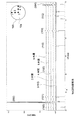
- FIG. 2 is a flowchart showing a process of manufacturing the target according to the present embodiment.
- 3 (a) to 3 (d) are schematic views showing a process of manufacturing a target corresponding to FIG.
- a cobalt material is melted by an electron beam in a crucible or the like, and after the melted cobalt material is cooled, a cobalt ingot 100i shown in FIG. 3A is formed. .
- the cobalt plate 100p is cooled to or near room temperature, and then the cobalt plate 100p is subjected to vacuum heating (first vacuum heating) at a temperature higher than 449 ° C.
- This 449 ° C. is a phase transition temperature of cobalt.
- the temperature of cobalt changes from a temperature lower than 449 ° C. to a temperature higher than 449 ° C.
- cobalt changes from a hexagonal close-packed lattice structure to a face-centered cubic structure.
- the cobalt plate 100p is heated in a vacuum.
- the cobalt plate 100p If, after performing hot rolling at 1000 ° C. or higher, the cobalt plate 100p is rapidly cooled to a temperature lower than the transition temperature, it can be transformed from the face-centered cubic structure to the hexagonal close-packed lattice structure by supercooling.
- the face-centered cubic structure that did not exist remains on the cobalt plate 100p. That is, a hexagonal close-packed lattice structure and a face-centered cubic structure are mixed in the quenched cobalt plate 100p. Then, even if the process proceeds to the subsequent process in this state, the state where the hexagonal close-packed lattice structure and the face-centered cubic structure coexist continues in the cobalt plate 100p.
- the present embodiment after performing hot rolling at 1000 ° C. or higher, vacuum heating is performed on the cobalt plate 100p at a temperature higher than the transition temperature. As a result, the crystal structure of the cobalt plate 100p is once reset to the face-centered cubic structure.
- the cobalt plate 100p is cooled in a vacuum. That is, since the cobalt plate 100p is cooled under the condition that there is no atmosphere such as an inert gas or air around the periphery of the cobalt plate 100p, the cobalt plate 100p is not rapidly cooled, but is gradually cooled over a long time.
- the temperature of the cobalt plate 100p becomes lower than the transition temperature, the face-centered cubic structure is changed to the hexagonal close-packed lattice structure, and the cobalt plate 100p having the hexagonal close-packed lattice structure is formed.
- cold rolling is performed on the cobalt sheet 100p.
- the cobalt plate 100p is regarded as a rectangular parallelepiped
- cold rolling is performed on each of the two sets of opposite sides of the rectangular parallelepiped. That is, cold rolling is performed in two orthogonal axial directions.
- the rolling reduction in this cold rolling is 17% or more and 35% or less, preferably 17% or more and 30% or less, and more preferably 17% or more and 25% or less.
- the rolling reduction is lower than 17%, the (002) plane and the (004) plane of the hexagonal close-packed lattice structure are warped and oriented from the sputtering surface 10a, and when the rolling reduction is higher than 35%, cracks occur in the cobalt plate 100p. Or may be undesirable.
- the easy magnetization axis C of the hexagonal close-packed lattice structure randomly oriented in the cobalt plate 100p is sputtered.
- the entire surface 10a is aligned in the thickness direction (C-axis direction) of the cobalt plate 100p. That is, the (002) plane and the (004) plane of the hexagonal close-packed lattice structure are oriented along the sputtering surface 10a over the entire area of the sputtering surface 10a.
- vacuum heating is again performed on the cobalt plate 100p at a temperature lower than the transition temperature (for example, 400 ° C. or more and less than 449 ° C.). Since this vacuum heating is performed at a temperature lower than the transition temperature, the cobalt plate 100p maintains a hexagonal close-packed lattice structure. Further, by this vacuum heating, a small amount of the face-centered cubic structure metastable in the cobalt plate 100p is transformed into a hexagonal close-packed lattice structure. Further, the stress applied to the cobalt plate 100p by the cold rolling is reduced by the vacuum heating.
- the transition temperature for example, 400 ° C. or more and less than 449 ° C.
- the cobalt plate 100p is cut into a predetermined shape to form the target 100.
- FIG. 4 shows the results of X-ray diffraction measurement of the target according to the present embodiment.
- a disk-shaped target was used as the target 100.
- the measurement points are a total of five points at each position of the outer periphery 1, the middle 2, the center 3, the middle 4, and the outer periphery 5 on the sputtering surface 10a.
- the angle formed by the line connecting the outer circumference 1 and the center 3 and the line connecting the outer circumference 5 and the center 3 is 90 °.
- the thickness of the target 100 is 3 mm, and the outer diameter is 400 mm.
- the X-ray diffraction measurement conditions are as follows. Scanning method: 2 ⁇ / ⁇ method Target: Cu Tube voltage: 40 kV Tube current: 100 mA Scan speed: 5 ° / min Sampling width: 0.02 ° Divergence slit: 1 ° Scattering slit: 1 ° Light receiving slit: 0.3mm
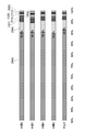
- FIG. 5 is a graph showing the ratio of the peak intensity of XRD. Here, the indication of 50% or less is omitted.
- FIG. 5 shows the (100), (002), (101), (102), (110), (103), and (112) planes of the hexagonal close-packed lattice structure at each measurement point. And the sum of the intensities of the X-ray diffraction peaks corresponding to the (004) plane (I (100) + I (002) + I (101) + I (102) + I (110) + I (103) + I (112) + I (004) ), The ratio (%) of the intensity I (002) + I (004) , which is the sum of the X-ray diffraction peaks corresponding to the (002) plane and the (004) plane.
- the average value of the ratio (%) of I (002) + I (004) shown in FIG. 5 was 95.1% as shown in Table 1. That is, the intensity ratio of the X-ray diffraction peak (I (002) + I (004) ) / (I (100) + I (002) + I (101) + I (102) + I (110) + I (103) + I in the target 100. It can be seen that (112) + I (004) ) is 0.85 or more as an average value of five measurements on the sputtering surface 10a.
- I derived the maximum value of I (002) + I (004 ) when the I max, the minimum value was I min, the formula A (I max -I min) / ( I max + I min) ( The variation ⁇ of ( 002) + I (004) was 0.008%, indicating excellent in-plane distribution characteristics.
- the half-value width of the peak belonging to the (002) plane of the hexagonal close-packed lattice structure is preferably 0.3 ° or less, and was 0.18 ° or less as an average value of five points measured.
- the variation ⁇ of the half width of the peak derived from Equation A was 0.06 °.
- the second vacuum heating when the second vacuum heating is omitted, a face-centered cubic structure may remain in the cobalt target, and a peak attributed to fcc (200) may be observed in the cobalt target.
- the average value of the half-value width of the peak attributed to fcc (200) of the cobalt target is 0.61 °, which is half of the peak attributed to the (002) plane of the hexagonal close-packed lattice structure.
- the average value of the value width is 0.50 °. Therefore, the ratio R of the half width of the peak belonging to hcp (002) to the half width of the peak belonging to fcc (200) of the cobalt target when the second vacuum heating is omitted is 0.82.
- the target 100 of the present embodiment is subjected to the second vacuum heating, even if a trace amount of the face-centered cubic structure remains, the target 100 belongs to fcc (200) as compared with the case where the second vacuum heating is not performed.
- the intensity of the peak that becomes weaker becomes weaker, and the half-value width of the peak attributed to fcc (200) becomes wider.
- the intensity of the peak belonging to hcp (002) becomes stronger, and the half-value width of the peak belonging to hcp (002) becomes narrower. Therefore, in the present embodiment, the ratio R can be estimated to be 0.82 or more.
- Table 1 shows the maximum relative magnetic permeability ( ⁇ max ) of the target in addition to the intensity ratio of the X-ray diffraction peak and the half-value width of the peak belonging to (002).
- the maximum relative magnetic permeability ⁇ max is the maximum value of the relative magnetic permeability along the sputtering surface 10a in the applied magnetic field range.
- the maximum relative magnetic permeability of the target 100 is in the range of 4.2 or more and 4.6 or less on the sputtering surface 10a.
- the variation ⁇ in the maximum relative magnetic permeability derived from the formula A was 0.045.
- the relative magnetic permeability along the sputtering surface 10a was less than 5, indicating an excellent relative magnetic permeability.
- 10a sputtering surface 10b: back surface 100, 101: target 100i: cobalt ingot 100b: cobalt block 100p: cobalt plate
Landscapes
- Chemical & Material Sciences (AREA)
- Engineering & Computer Science (AREA)
- Mechanical Engineering (AREA)
- Organic Chemistry (AREA)
- Materials Engineering (AREA)
- Metallurgy (AREA)
- Power Engineering (AREA)
- Chemical Kinetics & Catalysis (AREA)
- Physics & Mathematics (AREA)
- Thermal Sciences (AREA)
- Crystallography & Structural Chemistry (AREA)
- Manufacturing & Machinery (AREA)
- Manufacturing Of Magnetic Record Carriers (AREA)
- Physical Vapour Deposition (AREA)
Abstract
Description
走査方法:2θ/θ法
ターゲット:Cu
管電圧:40kV
管電流:100mA
スキャンスピード:5°/min
サンプリング幅:0.02°
発散slit:1°
散乱slit:1°
受光slit:0.3mm

10b…裏面
100、101…ターゲット
100i…コバルトインゴット
100b…コバルトブロック
100p…コバルト板
Claims (4)
- スパッタリング面を有し、純度が99.95wt%以上であるコバルトターゲットであり、
前記スパッタリング面に沿った六方最密格子構造の(100)面、(002)面、(101)面、(102)面、(110)面、(103)面、(112)面、及び(004)面に相当するX線回折ピークの強度比(I(002)+I(004))/(I(100)+I(002)+I(101)+I(102)+I(110)+I(103)+I(112)+I(004))が0.85以上である
スパッタリングターゲット。 - 請求項1に記載のスパッタリングターゲットであって、
前記スパッタリング面に沿った比透磁率が5未満である
スパッタリングターゲット。 - 請求項1~3のいずれか1つに記載のスパッタリングターゲットであって、
前記スパッタリング面に沿った六方最密格子構造の(002)面に相当するX線回折ピークの半値幅が0.3°以下である
スパッタリングターゲット。 - コバルトインゴットに対して熱間鍛造及び熱間圧延を行ってコバルト板を形成し、
前記コバルト板に対して、六方最密格子構造から面心立方構造に転移する転移温度よりも高い温度で第1真空加熱を行い、
前記コバルト板が前記転移温度よりも低い温度になるように前記コバルト板を真空冷却し、
前記コバルト板に対して、圧下率が17%以上35%以下になるように冷間圧延を行い、
前記コバルト板に対して、前記転移温度よりも低い温度で第2真空加熱を行う
スパッタリングターゲットの製造方法。
Priority Applications (4)
| Application Number | Priority Date | Filing Date | Title |
|---|---|---|---|
| KR1020207003711A KR102330578B1 (ko) | 2018-07-27 | 2019-03-28 | 스퍼터링 타겟 및 스퍼터링 타겟의 제조 방법 |
| JP2019536603A JP6698950B1 (ja) | 2018-07-27 | 2019-03-28 | スパッタリングターゲット及びスパッタリングターゲットの製造方法 |
| US16/759,149 US11421315B2 (en) | 2018-07-27 | 2019-03-28 | Sputtering target and method of producing sputtering target |
| CN201980004037.2A CN111051566B (zh) | 2018-07-27 | 2019-03-28 | 溅射靶及溅射靶的制造方法 |
Applications Claiming Priority (2)
| Application Number | Priority Date | Filing Date | Title |
|---|---|---|---|
| JP2018140853 | 2018-07-27 | ||
| JP2018-140853 | 2018-07-27 |
Publications (1)
| Publication Number | Publication Date |
|---|---|
| WO2020021772A1 true WO2020021772A1 (ja) | 2020-01-30 |
Family
ID=69180393
Family Applications (1)
| Application Number | Title | Priority Date | Filing Date |
|---|---|---|---|
| PCT/JP2019/013572 Ceased WO2020021772A1 (ja) | 2018-07-27 | 2019-03-28 | スパッタリングターゲット及びスパッタリングターゲットの製造方法 |
Country Status (6)
| Country | Link |
|---|---|
| US (1) | US11421315B2 (ja) |
| JP (1) | JP6698950B1 (ja) |
| KR (1) | KR102330578B1 (ja) |
| CN (1) | CN111051566B (ja) |
| TW (1) | TWI746992B (ja) |
| WO (1) | WO2020021772A1 (ja) |
Citations (4)
| Publication number | Priority date | Publication date | Assignee | Title |
|---|---|---|---|---|
| JP2001200356A (ja) * | 1999-11-01 | 2001-07-24 | Praxair St Technol Inc | 低透磁率コバルトスパッターターゲットの製造方法 |
| JP2001514325A (ja) * | 1997-08-26 | 2001-09-11 | ザ アルタ グループ インコーポレイテッド | 高純度コバルトスパッターターゲット及びその製造方法 |
| JP2003306751A (ja) * | 2002-04-16 | 2003-10-31 | Daido Steel Co Ltd | Co系スパッタリングターゲットの製造方法 |
| WO2014157187A1 (ja) * | 2013-03-27 | 2014-10-02 | Jx日鉱日石金属株式会社 | コバルトスパッタリングターゲット及びその製造方法 |
Family Cites Families (9)
| Publication number | Priority date | Publication date | Assignee | Title |
|---|---|---|---|---|
| JP4419346B2 (ja) * | 2001-06-27 | 2010-02-24 | 三菱マテリアル株式会社 | スパッタリングターゲット及びその配置方法 |
| JP2003073817A (ja) * | 2001-08-31 | 2003-03-12 | Mitsubishi Materials Corp | スパッタリングターゲット及びその配置方法 |
| CN100507071C (zh) * | 2003-12-31 | 2009-07-01 | 上海贝岭股份有限公司 | 一种用于制作磁性直流磁控溅射钴靶材的方法 |
| JP4963037B2 (ja) * | 2006-05-01 | 2012-06-27 | 株式会社アルバック | スパッタリング用コバルトターゲット及びその製造方法 |
| JP5204460B2 (ja) * | 2007-10-24 | 2013-06-05 | 三井金属鉱業株式会社 | 磁気記録膜用スパッタリングターゲットおよびその製造方法 |
| CN101429646B (zh) * | 2008-12-12 | 2012-06-27 | 厦门大学 | 无诱导磁场下产生面内单轴磁各向异性的薄膜的制备方法 |
| CN102634763A (zh) * | 2012-04-19 | 2012-08-15 | 同济大学 | 脉冲激光沉积制备四氧化三钴薄膜电极材料的方法及其应用 |
| CN103451586B (zh) * | 2012-06-01 | 2015-12-09 | 宁波江丰电子材料股份有限公司 | 钴靶材热处理方法 |
| CN104694894B (zh) * | 2013-12-05 | 2017-07-04 | 有研亿金新材料股份有限公司 | 一种高透磁钴靶及其制备方法 |
-
2019
- 2019-03-28 CN CN201980004037.2A patent/CN111051566B/zh active Active
- 2019-03-28 KR KR1020207003711A patent/KR102330578B1/ko active Active
- 2019-03-28 JP JP2019536603A patent/JP6698950B1/ja active Active
- 2019-03-28 WO PCT/JP2019/013572 patent/WO2020021772A1/ja not_active Ceased
- 2019-03-28 US US16/759,149 patent/US11421315B2/en active Active
- 2019-06-14 TW TW108120577A patent/TWI746992B/zh active
Patent Citations (4)
| Publication number | Priority date | Publication date | Assignee | Title |
|---|---|---|---|---|
| JP2001514325A (ja) * | 1997-08-26 | 2001-09-11 | ザ アルタ グループ インコーポレイテッド | 高純度コバルトスパッターターゲット及びその製造方法 |
| JP2001200356A (ja) * | 1999-11-01 | 2001-07-24 | Praxair St Technol Inc | 低透磁率コバルトスパッターターゲットの製造方法 |
| JP2003306751A (ja) * | 2002-04-16 | 2003-10-31 | Daido Steel Co Ltd | Co系スパッタリングターゲットの製造方法 |
| WO2014157187A1 (ja) * | 2013-03-27 | 2014-10-02 | Jx日鉱日石金属株式会社 | コバルトスパッタリングターゲット及びその製造方法 |
Also Published As
| Publication number | Publication date |
|---|---|
| JP6698950B1 (ja) | 2020-05-27 |
| JPWO2020021772A1 (ja) | 2020-08-06 |
| KR20200028421A (ko) | 2020-03-16 |
| CN111051566B (zh) | 2021-11-09 |
| US11421315B2 (en) | 2022-08-23 |
| KR102330578B1 (ko) | 2021-11-24 |
| US20210172056A1 (en) | 2021-06-10 |
| TWI746992B (zh) | 2021-11-21 |
| CN111051566A (zh) | 2020-04-21 |
| TW202014529A (zh) | 2020-04-16 |
Similar Documents
| Publication | Publication Date | Title |
|---|---|---|
| JP2020004969A (ja) | 保磁力傾斜型Nd−Fe−B系磁性体及びその製造方法 | |
| KR20190100915A (ko) | 육방정 질화붕소 박막과 그 제조 방법 | |
| JP2010013678A (ja) | 銅スパッタリングターゲット材及びスパッタリング方法 | |
| JP2018016823A (ja) | 放熱部材用銅合金板材およびその製造方法 | |
| KR101991150B1 (ko) | 코발트 스퍼터링 타깃 및 그 제조 방법 | |
| JP2018046277A (ja) | 窒化ガリウム系膜ならびにその製造方法 | |
| JP4963037B2 (ja) | スパッタリング用コバルトターゲット及びその製造方法 | |
| WO2020054104A1 (ja) | MgO焼結体スパッタリングターゲット | |
| JP6698950B1 (ja) | スパッタリングターゲット及びスパッタリングターゲットの製造方法 | |
| JP6340621B2 (ja) | Niスパッタリングターゲット及びその製造方法 | |
| US11072842B2 (en) | Rare earth thin film magnet and method for producing same | |
| JPWO2014038022A1 (ja) | Nd−Fe−B薄膜磁石およびその製造方法 | |
| Tong et al. | The effects of the growth pressure and annealing conditions on perpendicular magnetic anisotropy of sputtered NdFeCo films on Si (1 1 1) | |
| JP2017098538A (ja) | Mn−X系磁性材料 | |
| CN108624852B (zh) | 一种高居里温度的铁锆非晶多层膜及其制备方法 | |
| Wang et al. | Effect of high magnetic fields on the morphology of soft magnetic α′-FeN films | |
| Moskalev et al. | Structural investigation of magnetron sputtered Ta/NixMn100-x/Ta thin films | |
| JP6631029B2 (ja) | 永久磁石、及び、それを備えた回転機 | |
| Min et al. | Control of stress and plasma-induced heating during dc magnetron sputtering of permalloy films for microelectromechanical systems | |
| JP6261075B2 (ja) | 磁気力顕微鏡用探針の製造方法 | |
| Yang et al. | Characteristics of Ni films deposited on SiO2/Si (1 0 0) and MgO (0 0 1) by direct current magnetron sputtering system with the oblique target | |
| Li et al. | Sputtering pressure effects on microstructure and grain orientation distribution in FePt thin films | |
| JP5567042B2 (ja) | Tft用銅スパッタリングターゲット材 | |
| Tunaboylu et al. | Phase transformation and paired-plate precipitate formation in Pb0. 91La0. 09Zr0. 65Ti0. 35O3 films grown on sapphire substrates | |
| JP2017183319A (ja) | マンガンアルミニウム系磁石 |
Legal Events
| Date | Code | Title | Description |
|---|---|---|---|
| ENP | Entry into the national phase |
Ref document number: 2019536603 Country of ref document: JP Kind code of ref document: A |
|
| ENP | Entry into the national phase |
Ref document number: 20207003711 Country of ref document: KR Kind code of ref document: A |
|
| 121 | Ep: the epo has been informed by wipo that ep was designated in this application |
Ref document number: 19841297 Country of ref document: EP Kind code of ref document: A1 |
|
| NENP | Non-entry into the national phase |
Ref country code: DE |
|
| 122 | Ep: pct application non-entry in european phase |
Ref document number: 19841297 Country of ref document: EP Kind code of ref document: A1 |