WO2020003458A1 - 半導体検査装置 - Google Patents
半導体検査装置 Download PDFInfo
- Publication number
- WO2020003458A1 WO2020003458A1 PCT/JP2018/024678 JP2018024678W WO2020003458A1 WO 2020003458 A1 WO2020003458 A1 WO 2020003458A1 JP 2018024678 W JP2018024678 W JP 2018024678W WO 2020003458 A1 WO2020003458 A1 WO 2020003458A1
- Authority
- WO
- WIPO (PCT)
- Prior art keywords
- measurement
- electron beam
- sample
- output
- irradiation
- Prior art date
- Legal status (The legal status is an assumption and is not a legal conclusion. Google has not performed a legal analysis and makes no representation as to the accuracy of the status listed.)
- Ceased
Links
Images














Classifications
-
- G—PHYSICS
- G01—MEASURING; TESTING
- G01R—MEASURING ELECTRIC VARIABLES; MEASURING MAGNETIC VARIABLES
- G01R31/00—Arrangements for testing electric properties; Arrangements for locating electric faults; Arrangements for electrical testing characterised by what is being tested not provided for elsewhere
- G01R31/28—Testing of electronic circuits, e.g. by signal tracer
- G01R31/302—Contactless testing
- G01R31/305—Contactless testing using electron beams
- G01R31/307—Contactless testing using electron beams of integrated circuits
-
- G—PHYSICS
- G01—MEASURING; TESTING
- G01R—MEASURING ELECTRIC VARIABLES; MEASURING MAGNETIC VARIABLES
- G01R31/00—Arrangements for testing electric properties; Arrangements for locating electric faults; Arrangements for electrical testing characterised by what is being tested not provided for elsewhere
- G01R31/28—Testing of electronic circuits, e.g. by signal tracer
- G01R31/302—Contactless testing
- G01R31/305—Contactless testing using electron beams
-
- G—PHYSICS
- G01—MEASURING; TESTING
- G01R—MEASURING ELECTRIC VARIABLES; MEASURING MAGNETIC VARIABLES
- G01R31/00—Arrangements for testing electric properties; Arrangements for locating electric faults; Arrangements for electrical testing characterised by what is being tested not provided for elsewhere
- G01R31/28—Testing of electronic circuits, e.g. by signal tracer
- G01R31/2851—Testing of integrated circuits [IC]
- G01R31/2855—Environmental, reliability or burn-in testing
- G01R31/286—External aspects, e.g. related to chambers, contacting devices or handlers
- G01R31/2868—Complete testing stations; systems; procedures; software aspects
-
- G—PHYSICS
- G01—MEASURING; TESTING
- G01R—MEASURING ELECTRIC VARIABLES; MEASURING MAGNETIC VARIABLES
- G01R31/00—Arrangements for testing electric properties; Arrangements for locating electric faults; Arrangements for electrical testing characterised by what is being tested not provided for elsewhere
- G01R31/28—Testing of electronic circuits, e.g. by signal tracer
- G01R31/2851—Testing of integrated circuits [IC]
- G01R31/2882—Testing timing characteristics
-
- G—PHYSICS
- G01—MEASURING; TESTING
- G01R—MEASURING ELECTRIC VARIABLES; MEASURING MAGNETIC VARIABLES
- G01R31/00—Arrangements for testing electric properties; Arrangements for locating electric faults; Arrangements for electrical testing characterised by what is being tested not provided for elsewhere
- G01R31/28—Testing of electronic circuits, e.g. by signal tracer
- G01R31/317—Testing of digital circuits
- G01R31/31728—Optical aspects, e.g. opto-electronics used for testing, optical signal transmission for testing electronic circuits, electro-optic components to be tested in combination with electronic circuits, measuring light emission of digital circuits
-
- G—PHYSICS
- G01—MEASURING; TESTING
- G01R—MEASURING ELECTRIC VARIABLES; MEASURING MAGNETIC VARIABLES
- G01R31/00—Arrangements for testing electric properties; Arrangements for locating electric faults; Arrangements for electrical testing characterised by what is being tested not provided for elsewhere
- G01R31/28—Testing of electronic circuits, e.g. by signal tracer
- G01R31/317—Testing of digital circuits
- G01R31/3181—Functional testing
- G01R31/3183—Generation of test inputs, e.g. test vectors, patterns or sequences
-
- G—PHYSICS
- G01—MEASURING; TESTING
- G01R—MEASURING ELECTRIC VARIABLES; MEASURING MAGNETIC VARIABLES
- G01R31/00—Arrangements for testing electric properties; Arrangements for locating electric faults; Arrangements for electrical testing characterised by what is being tested not provided for elsewhere
- G01R31/28—Testing of electronic circuits, e.g. by signal tracer
- G01R31/302—Contactless testing
- G01R31/308—Contactless testing using non-ionising electromagnetic radiation, e.g. optical radiation
- G01R31/311—Contactless testing using non-ionising electromagnetic radiation, e.g. optical radiation of integrated circuits
Definitions
- the present invention relates to a semiconductor inspection apparatus, and more particularly, to a semiconductor device failure analysis technique using a microdevice characteristic evaluation apparatus using an electron microscope.
- LSIs large-scale integrated circuits
- the number of transistors, the number of wirings, and the number of contacts increase, and the failure analysis of a failed device becomes complicated, and the sensitivity of failure detection technology for a small device is increased. Is required.
- a micro device refers to a microstructure such as an element integrated in an LSI or a wiring formed in the LSI.
- a failure detection technique a nanoprobing apparatus that measures electrical characteristics by directly contacting a measurement probe with a fine area has attracted attention. According to this, a measurement probe can be brought into direct contact with a terminal of a nanodevice such as a transistor of a 10 nm generation process, and its electrical characteristics can be evaluated, which is a great feature not found in other analysis techniques.
- EBAC Electro Beam Absorption Current
- an absorption current flowing locally between the irradiation position of the electron beam and the measurement probe is detected, and the obtained change in the signal amount is associated with the scanning of the electron beam as a contrast, so that an image (EBAC image) is obtained.
- the EBAC image can be visualized including the internal information of the measurement sample, for example, the shape of the wiring formed in the depth direction of the sample. If there is a break in the wiring, the amount of absorption current detection depends on whether the electron beam irradiation position is on the wiring before the break or on the wiring beyond the break, as viewed from the contact point of the measuring probe. EBAC images are expressed with different contrasts. As a result, it is possible to easily grasp the failure location of the device without destroying the defective portion.
- EBAC observation has the following problems.
- (1) The contrast of an EBAC image is low for a defect having low resistance, and it is difficult to detect a defect portion. For example, taking a wiring failure as an example, in the case of an open fault such as a disconnection, a defective portion has a high resistance and a strong contrast can be obtained. Difficult to detect.
- an EBIC Electro Beam Induced Current
- the EBIC is a drift current generated by electrons and holes generated when an electron beam enters the vicinity of the junction, and a signal due to the EBIC reaction is a very strong current signal.
- the current signal flowing into the EBAC apparatus ranges from about 10 nA due to the EBIC reaction to about 0.001 nA due to the structure portion through which a small amount of current flows. Even if such a wide-range signal is divided into, for example, 256 gradations to display the density of an image, the fineness of the information is lost, and the information is easily lost.
- an amplifier used for EBAC observation may be saturated due to an excessive current flowing, and a difference in contrast cannot be displayed in a saturated region. In such a case, the current distribution information that should be obtained originally is missing, and as a result, it becomes difficult to physically interpret the phenomenon occurring in the microdevice.
- an advantage of using a nanoprobing apparatus is that various electrical characteristics of a micro device can be measured, and device failure analysis can be performed from various viewpoints. Therefore, there is provided a semiconductor inspection apparatus capable of executing an analysis using a plurality of electric characteristic map images or an analysis using an electric characteristic map image in cooperation with an analysis using another analysis method.
- a semiconductor inspection apparatus includes a sample table on which a sample is placed, an electron optical system that irradiates the sample with an electron beam, a measurement probe that is in contact with the sample, and a measurement probe from the measurement probe.
- the timing of starting the irradiation and the timing of freezing the irradiation of the electron beam, the first measurement period in which the measuring instrument measures the output from the measurement probe in a state where the electron beam is irradiated on the sample, and the irradiation of the electron beam A second measurement period in which the measuring instrument measures the output from the measurement probe after the freeze is set, and the measured value of the output from the measurement probe in response to the irradiation of the sample with the electron beam is set to the first measurement period.
- a first measurement value measured during a measurement period and a first measurement value measured during a second measurement period Determined from the difference between the second measurement value.
- a semiconductor inspection apparatus is a sample stage on which a sample is placed, an electron optical system that irradiates the sample with an electron beam, and a measurement probe that is in contact with the sample, A measuring device that measures the output from the measuring probe, a detector that detects signal electrons emitted by the interaction between the electron beam and the sample, and an output from the measuring probe in response to the irradiation of the sample with the electron beam.
- An electronic information system scans the sample two-dimensionally under the first imaging condition, and the information processing device creates an SEM image from a signal detected by the detector.
- virtual coordinates are set based on the SEM image
- the electron optical system scans the sample two-dimensionally under the second imaging condition
- the information processing apparatus measures the output from the measurement probe measured by the measuring instrument.
- the information processing device By coordinate transformation based the virtual coordinates to the first imaging condition and the second imaging condition, to identify on the electrical characteristic map image the position specified by the virtual coordinates.
- FIG. 7 is a diagram illustrating a time change of a voltage signal and a measurement timing in that case.
- FIG. 7 is a diagram illustrating a time change of a current signal and a measurement timing in that case.
- FIG. 5 is a diagram for explaining a method of calculating a measurement value in voltage mapping measurement. It is an example of a sample.
- FIG. 7 is a schematic diagram of an EBAC image of the sample shown in FIG. 6.
- FIG. 9 is a diagram illustrating resistance dependence of a gradation difference in an EBAC image. 2 is an example of measurement by the measurement circuit of FIG.
- FIG. 10 is current distribution data corresponding to the EBAC image shown in FIG. 2 is an example of measurement by the measurement circuit of FIG.
- FIG. 1 is a schematic diagram of a micro device characteristic evaluation device of a first embodiment. It is a schematic diagram of a micro device characteristic evaluation device of a second embodiment.
- FIG. 9 is a schematic diagram of a micro device characteristic evaluation device according to a third embodiment. It is a schematic diagram of a micro device characteristic evaluation device of a fourth embodiment. It is the schematic of the micro device characteristic evaluation apparatus of 5th Example. It is the schematic of the micro device characteristic evaluation apparatus of a 6th Example. It is the schematic of the micro device characteristic evaluation apparatus of 7th Example. It is a figure explaining the probing position setting operation in an 8th example.
- FIG. 1 is a schematic diagram of a micro device characteristic evaluation apparatus according to an embodiment of the present invention.
- the scanning electron microscope has an electron optical system 1, a detector 2, and a vacuum chamber 4 as its main components, and is controlled by a control device 12 connected by a communication cable 14.
- a measurement sample 5 is placed on a sample table 6 in a vacuum chamber 4, and the measurement probe 3 is in contact with the measurement sample 5.
- the measurement probe 3 is connected to a driving device (not shown) for moving the sample surface of the measurement sample 5, and is brought into contact with the measurement sample 5 by the operation of the driving device.
- the output of the measurement probe 3 is connected to the differential amplifier 7 through the measurement cable 13, and the output signal of the differential amplifier 7 is input to the semiconductor parameter analyzer 8.
- the semiconductor parameter analyzer 8 is a measuring device for a parametric test of a semiconductor device such as a current-voltage measurement and a capacitance measurement. A measuring instrument according to the measurement object and the content of the measurement may be used.
- the semiconductor parameter analyzer 8 is connected to the information processing device 9 through a communication cable 14.
- the cable for transmitting the analog signal is referred to as a measurement cable 13 (solid line)
- the cable for transmitting the digital signal is referred to as a communication cable 14 (solid line).
- the transfer characteristics, communication protocols, and the like may be different for each connected device.
- the information processing device 9 controls the electron microscope, and creates and displays an SEM image from a signal detected from the detector 2, an EBAC image from a signal detected from the measurement probe 3, and an electric characteristic map image of the present embodiment.
- a personal computer or the like can be applied.
- the detector 2 detects signal electrons emitted by the interaction between the electron beam from the electron optical system 1 and the measurement sample 5. A plurality of detectors may be provided according to differences in the energy of signal electrons to be detected.
- the amplification factor of the differential amplifier 7 is controlled by the information processing device 9. Thus, when the output signal of the differential amplifier 7 is excessive, the amplification factor can be reduced.
- the measuring circuit in FIG. 1 has a configuration suitable for measuring a voltage as an electric characteristic and creating a voltage map image as an electric characteristic map image. Further, the voltage map image in the present embodiment can obtain high detection sensitivity for low-resistance defects as described later, and is therefore suitable for defect detection and failure analysis of low-resistance metal wiring and the like.
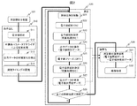
- FIG. 2 shows a flow of creating a voltage map image by the micro device characteristic evaluation device of FIG.
- the flow mainly includes condition setting for measurement (S10), measurement (S20), and imaging of measured values (S30).
- S10 condition setting for measurement
- S20 measurement
- S30 imaging of measured values
- an electron beam is irradiated to an arbitrary position on the sample surface (S11).
- the signal of the measurement probe obtained as a result is amplified by the differential amplifier 7, and high-frequency random noise is removed from the voltage signal using the integration processing of the semiconductor parameter analyzer 8 (S12).
- the integration process is a process in which signals mixed with random noise are added for a predetermined period and averaged as shown in FIG. Thereby, the influence of random noise can be removed.
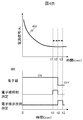
- FIG. 4A shows a pattern observed at the time of voltage measurement, which is a low-frequency noise unique to the microdevice characteristic evaluation apparatus.
- the output signal (voltage signal) drifts due to the influence of vibration of an exhaust pump for exhausting the vacuum chamber 4 or electric noise of the evaluation device. In addition, it is not only the voltage signal that is affected by such low frequency noise.
- a current map image is created as an electric characteristic map image, a current signal is detected (the configuration of the device in that case will be described later). However, the current signal also has low frequency noise.
- FIG. 4B is a pattern observed at the time of current measurement, and shows a change in an output signal (current signal) having a time constant due to the capacitance when the measurement sample 5 is a high-resistance sample (such as a semiconductor).
- the information processing device 9 obtains a time zone having the least time change from the time change of the voltage signal data (or the current signal data) of the measurement sample 5 from which the random noise has been removed, for example, by differential analysis.
- time zones t1 to t3 can be detected as time zones with little time change. Therefore, the measurement timing is set so that the measurement is performed during the time period t1 to t3 (S14).
- a measurement timing chart for the signal waveform 401 is 403
- a measurement timing chart for the signal waveform 402 is 404.
- the irradiation of the electron beam to the measurement sample 5 is frozen at t2 between the time zones t1 and t3, and the time zones t1 and t2 immediately before that and the time zones t2 and t3 immediately after that.
- the output signal is measured at.
- Each of the time zones t1 to t2 and each of the time zones t2 to t3 must have a time for performing an integration process for removing high-frequency random noise.
- FIG. 5 shows a state of the measurement.
- the measurement probe 3 is in contact with one point 502 of the sample surface 501, and the electron beam 500 scans on the sample surface 501 in the X direction and the Y direction.
- a cell virtually shown on the sample surface 501 indicates the irradiation position of the electron beam 500, and corresponds to one pixel of the voltage map image.
- the irradiation position is moved to, for example, the position 503 (S21), and irradiation of the electron beam 500 is started (S22).
- the output signal is measured at the measurement timings t1 to t2 determined in the condition setting (S23).
- the information processing device 9 stores the output data (herein referred to as “electron beam irradiation data”) on which the integration process has been performed in the database 11 (S24). Subsequently, at time t2, the irradiation of the position 503 of the electron beam 500 is frozen (S25), and the output signal is measured at the measurement timings t2 to t3 determined in the condition setting (S26). Also in this measurement, the integration processing by the semiconductor parameter analyzer 8 is performed. The information processing device 9 stores the output data (herein referred to as “electron beam non-irradiation data”) on which the integration process has been performed in the database 11 (S27).
- the information processing device 9 determines whether irradiation and measurement have been completed at all irradiation positions (S28), and moves to the next irradiation position if not completed. For example, the irradiation position is moved to a position 504 adjacent to the position 503 in the X direction (S21), and irradiation with the electron beam 500 is started (S22). When the irradiation of the electron beam to all the irradiation positions and the measurement have been completed, the measurement is terminated, and the measurement results at all the irradiation positions are stored in the database 11.
- the flow of the measurement (S20) in FIG. 2 shows a large flow, and is not limited to this.
- the electron beam irradiation data and the electron beam non-irradiation data do not need to be stored in the database 11 for each irradiation, but are stored in a unit.
- the information processing device 9 temporarily stores the data and completes the measurement. You may make it save in the database 11 later.
- the information processing device 9 controls the gain of the differential amplifier 7 so that the measurement by the semiconductor parameter analyzer 8 can be appropriately performed, the output data is not converted to the output value of the semiconductor parameter analyzer 8 but to the differential amplifier 7. It is desirable to store a value obtained by correcting the gain of the above as output data.
- the output data and the gain of the differential amplifier 7 may be stored as a set.
- Imaging (S30) is performed using the electron beam irradiation data and the electron beam non-irradiation data obtained in the measurement (S20).
- the difference between the electron beam irradiation data and the electron beam non-irradiation data is calculated as a measured value (S31).
- This operation removes the influence of low frequency noise from the measured value.
- the measurer can display the numerical value according to the analysis viewpoint.
- a numerical mapping image can be created and displayed.
- loss of information such as crushed black can be avoided, and wide-range analysis can be performed.
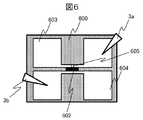
- FIG. 6 shows an example of a sample used as an analysis target.
- a resistor 602 is formed over an insulator layer 600, and electrodes 603 and 604 are provided with the resistor 602 interposed therebetween.
- the measurement probe 3a connected to the + terminal of the differential amplifier 7 is in contact with the electrode 603, and the measurement probe 3b connected to the-terminal of the differential amplifier 7 is in contact with the electrode 604.
- the insulator layer 600 is formed of a SiO 2 layer
- the resistor 602 is formed of Si
- the electrodes 603 and 604 are formed of Al.
- a plurality of samples having different resistance values were prepared as the resistance value of the resistor 602.
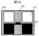
- FIG. 7A When the sample shown in FIG. 6 is observed by EBAC, when the resistance value of the resistor 602 is high (for example, on the order of several tens of k ⁇ ), as shown in FIG. 7A, the EBAC image 610 is separated from the resistor 602 by a boundary. Strong contrast is displayed. From this, it can be determined that there is a resistor at the contrast change point. This corresponds to performing an open fault defect detection in the failure analysis of the semiconductor device. However, as the resistance value of the resistor 602 decreases, the difference between the high contrast portion 611 and the low contrast portion 613 decreases.
- FIG. 7B is a diagram illustrating the resistance dependence of the gradation difference in the EBAC image 610.
- the horizontal axis represents the resistance value of the resistor 602
- the vertical axis represents the gradation difference between the low contrast portion 613 and the background portion 612 corresponding to the insulator layer 600.
- the electron dose (probe current) applied to the sample is 1 nA.
- the gradation difference from the background portion 612 increases, and when the resistance value of the resistor 602 is on the order of several hundred ⁇ , the resistance value of the resistor 602 changes.
- the gradation difference 620 becomes very small. For this reason, it is impossible to visually recognize the contrast difference from the EBAC image.
- the voltage generated when a 100 ⁇ resistor is irradiated with an electron beam with an electron dose of 1 nA is 0.1 ⁇ V. Therefore, in order to enable detection of a defect such as a short-circuit of a wiring, a very small voltage of about 0.1 ⁇ V is required. It is necessary to determine the difference between the voltage signals.
- FIG. 8 shows the result of measurement of the same sample using the measurement circuit in the micro device characteristic evaluation device of FIG.
- FIG. 8 shows a voltage signal amount measured by the semiconductor parameter analyzer 8 in the measurement circuit in FIG. 1 when the region of the electrode 603 or the electrode 604 is irradiated with an electron beam in the sample shown in FIG.
- the measurement was performed on three types of samples in which the resistance value of the resistor 602 was 803 ⁇ , 290 ⁇ , and 186 ⁇ , respectively.
- the position of the measurement probe 3 was as shown in FIG. 6, and the irradiation current of the electron beam was also 1 nA, which was the same as in the above-mentioned EBAC observation.
- the gain of the differential amplifier 7 is set to 1000 times, and the measuring method is as described with reference to FIGS.
- the voltage map image of the present embodiment can be formed by shading the magnitude of the voltage signal amount to obtain a pixel value at the electron beam irradiation position.
- a result using a voltage amplifier (gain 100000 times) instead of the differential amplifier 7 is also shown.
- the absolute value of the voltage value output from the differential amplifier 7 tends to decrease as the resistance value of the resistor 602 decreases.
- the fact that such a difference in resistance can be detected by the measurement circuit of the present embodiment means that abnormality detection of a low resistance failure has become possible.
- the voltage amplifier shown as the comparative example the data was buried in the noise, and the value could not be obtained.
- the minimum measuring voltage of a general measuring instrument used for a parametric test of a semiconductor device is about 0.5 ⁇ V.
- the measurement circuit of the present embodiment enables a small difference of about 0.1 ⁇ V between the voltage signals. For this reason, the measurement circuit of the present embodiment thoroughly removed noise. Since the differential amplifier 7 amplifies the difference between the two measurement cables, it is possible to remove noise applied to both measurement cables in the same manner. Next, as described above, the integrating process is performed by the measuring device, and the random noise that cannot be removed by the differential amplifier 7 is removed. Furthermore, low-frequency noise is removed by measuring at the measurement timing determined by the condition setting described with reference to FIG.
- the types of noise that can be dealt with are each determined for the noise removal method, and high sensitivity detection is realized by utilizing a wide range of methods.
- the information processing device 9 adjusts the amplification factor of the differential amplifier 7 or the integrated amount by a measuring device. As described above, the information processing device 9 not only acquires and processes the measurement data, but also plays a role of providing an optimal noise removal step according to the type of noise included in the measurement data.
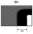
- FIG. 9 is an example of an EBAC image obtained by observing a semiconductor layer.
- the darkened portion 900 is a reaction from the semiconductor layer.
- FIG. 10 shows the result of measurement using the measurement circuit in the micro device characteristic evaluation apparatus of FIG. This is a graph obtained by measuring the current value of a portion 900 of a blackened portion. From this, it can be recognized that although the EBAC image has been blackened, a current change exists in that region. As described above, detailed information can be obtained even in an area where information cannot be obtained from the EBAC image, and physical interpretation in such an area can be performed.
- the contrast of the EBAC image is based on the amount of absorption current.
- the amount of absorbed current changes depending on the nanoscale internal structure of the measurement sample and the complicated behavior of the incident electrons, and thus, only visual observation of the contrast limits the information obtained.
- the present embodiment since the voltage value can be accurately measured by the micro device characteristic evaluation apparatus of FIG. 1, the present embodiment has a potential to obtain information that cannot be obtained by the conventional EBAC image. I have.
- FIG. 11 shows voltage values measured by irradiating the position 605 shown in FIG. 6 with an electron beam for each sample.
- the horizontal axis shows the resistance value of the resistor 602
- the vertical axis shows the voltage value (however, this voltage value is a value after amplification by a differential amplifier).
- FIG. 11 it was found that the six samples were divided into two groups by making a graph focusing on the numerical value of the voltage value.
- the two groups differed in the size of the resistor 602.
- the group 701 had a resistor width of 10 ⁇ m
- the group 702 had a resistor width of 1 ⁇ m.
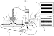
- FIG. 12 shows a first embodiment of the micro device characteristic evaluation apparatus.
- the differential amplifier 7 is connected to the semiconductor parameter analyzer 8 and the EBAC control device 21 through the switch 20. By this switching, it is possible to switch between electric characteristic map observation and EBAC observation.
- the EBAC control device 21 outputs the output of the differential amplifier 7 as a signal indicating the amount of absorption current at the irradiation position of the electron beam, and causes the information processing device 9 to image the EBAC image 22.
- the measurement circuit in the micro device characteristic evaluation apparatus shown in FIG. 12 is adapted to the low-resistance failure analysis that is difficult to detect in the EBAC image, and detects and analyzes defects in the wiring structure of the LSI device. Can be used for such.
- polishing is performed until the measurement contact of the LSI device comes to the surface.
- the polished LSI device is used as a measurement sample 5, and the measurement probe 3 is brought into contact with the contact exposed on the surface.
- the output of the differential amplifier 7 is switched to the EBAC control device 21, and the desired Search for the wiring section.
- the output of the differential amplifier 7 is switched to the semiconductor parameter analyzer 8, the observation is switched to the voltage map observation, and the voltage map image 15 is used for detailed analysis.
- the semiconductor parameter analyzer 8 the observation is switched to the voltage map observation, and the voltage map image 15 is used for detailed analysis.
- FIG. 13 shows a second embodiment of the micro device characteristic evaluation apparatus.
- This embodiment relates to a GUI (Graphical User Interface) of a micro device characteristic evaluation apparatus, in order to analyze an electric characteristic map image in detail, designates a part of the electric characteristic map image from a user interface, and measures a designated portion. Display values graphically. As a result, the details of the point of interest can be immediately grasped as numerical data, which is useful for analyzing an electrical phenomenon occurring in the sample.
- GUI Graphic User Interface
- the analysis data of the present embodiment is displayed on the two-screen monitors 10a and 10b.
- a linear mark 25 can be drawn on the GUI on the voltage map image 15 displayed on the monitor 10b.
- the information processing device 9 specifies the position specified by the mark 25 on the voltage map image 15 and displays the measured value of the position as a graph 26 on the monitor 10b.
- the graph 26 displays the position specified by the mark 25 on the horizontal axis and the measured value (voltage value in this case) at that position on the vertical axis.
- FIG. 14 shows a third embodiment of the micro device characteristic evaluation apparatus.
- the present embodiment also enables the GUI of the micro device characteristic evaluation apparatus to perform an electric characteristic map observation on a plurality of samples and to compare the observation results (electric characteristic map images) side by side. Further, a predetermined portion of the electric characteristic map image is designated from the user interface, and the measured value of this portion is displayed as a graph.
- the analysis data of the present embodiment is also displayed on the two-screen monitors 10a and 10b.
- the voltage map images 15a to 15d displayed on the screen monitor 10b point marks 30a to 30d for the user to specify the positions to be compared can be specified on the GUI.
- the measured value at the specified position is extracted from the database 11, and the monitor 10a sets the measured value at the specified position (in this case, the voltage value) on the monitor 10a and the horizontal axis indicates the name of the sample to be compared. It is displayed as a graph 31.
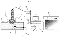
- FIG. 15 shows a fourth embodiment of the micro device characteristic evaluation apparatus.
- a current signal is acquired from the measurement probe 3 and a current map image 35 is created.
- the output of the measuring probe 3 is connected to the semiconductor parameter analyzer 8 through the measuring cable 13.
- Observation using the voltage map image assumes detection of an abnormality in the low-resistance wiring structure of the LSI device, whereas observation using the current map image assumes detection of an abnormality in the PN junction of the semiconductor layer of the LSI device. Since the measurement accuracy of a measuring instrument for a parametric test of a general semiconductor device such as the semiconductor parameter analyzer 8 has sufficient accuracy for the present application, the measuring circuit of the present embodiment uses the measuring probe 3 The output is connected to the semiconductor parameter analyzer 8 as it is.
- the current distribution amount of the semiconductor layer can be observed by observing the current map image of the semiconductor layer. By comparing this with a semiconductor simulation or the like, a semiconductor structure such as a doping amount can be estimated.
- FIG. 16 shows a fifth embodiment of the micro device characteristic evaluation apparatus.
- the present embodiment is a micro device characteristic evaluation apparatus that creates a pulse response map image 41 as an electric characteristic map image.
- the output of the measurement probe 3 is connected to the oscilloscope 40 through the measurement cable 13.
- the oscilloscope 40 is connected to the information processing device 9 through the communication cable 14.
- an incident electron beam to be irradiated is incident at a predetermined interval and a pulse width.
- the oscilloscope 40 measures a probe current 42 generated in a pulse form by the pulsed electron beam, measures a pulse rise time 43, and transmits the pulse data to the information processing apparatus 9 as numerical data.
- the information processing device 9 determines the pixel value of each pixel by dividing the pulse rise time 43 measured by the oscilloscope 40 into, for example, 256 gradations, and creates a pulse response map image 41 as a numerical mapping image.
- the pulse response map image 41 shown in FIG. 16 schematically shows an image observed for the wiring structure of the LSI device.
- the metal wiring portion is displayed in black because the pulse probe current rises rapidly, whereas the insulating layer portion is basically displayed in white.
- the region 44 where the metal wirings are close to each other has a capacitance component, a contrast according to the magnitude of the capacitance component appears.
- the inter-wiring capacitance causing signal delay and noise can be observed from the pulse response map image 41.
- Abnormalities can be analyzed from the contrast appearing in the pulse response map image, and abnormalities can be analyzed by comparing a normal device sample with a defective device sample.
- the present invention is not limited to this example, and the pulse response characteristic in response to irradiation with the pulsed electron beam can be broadly measured as the electrical characteristic. .
- the pulse response characteristic in response to irradiation with the pulsed electron beam can be broadly measured as the electrical characteristic.
- measurement of a pulse width, a pulse current value, and the like can be considered.
- FIG. 17 shows a sixth embodiment of the micro device characteristic evaluation apparatus.
- a sectional voltage map image is created.
- the measurement sample is a sample 45 obtained by obliquely polishing a bare silicon wafer into which oxygen ions have been implanted.
- An electrode 46 for measuring electric characteristics is provided on the front surface of the sample table 6 from the back surface of the sample 45, and the sample 45 is mounted on the electrode 46.
- the semiconductor parameter analyzer 8 By bringing the measurement probe 3 into contact with the electrode 46, a change in potential on the back surface of the sample 45 can be measured by the semiconductor parameter analyzer 8.
- the output of the measurement probe 3 is directly connected to the semiconductor parameter analyzer 8 through the measurement cable 13 in order to measure a high resistance sample called a bare silicon wafer.
- a differential amplifier is not used, measurement is performed according to the flowchart of FIG. 2 in order to remove the influence of high frequency random noise and low frequency noise.
- the measurement accuracy is enhanced by making the reference potential of the vacuum chamber 4 and the reference potential of the semiconductor parameter analyzer 8 common.
- the surface of the sample 45 polished obliquely is irradiated with an electron beam.
- the potential V1 is measured from the measurement probe 3 by irradiating the first electron beam irradiation position P1 with the electron beam.
- the electron beam is scanned, and the irradiation position P2 is irradiated with the electron beam to measure the potential V2.
- a value obtained by subtracting the potential V1 from the potential V2 is a potential difference Vmap1 between the depth position Pd2 (the position in the depth direction of the irradiation position P2, the same applies hereinafter) and the depth position Pd1, and the potential difference Vmap1 is determined by the position.
- the potential V3 is measured by irradiating the irradiation position P3 with an electron beam.
- the value obtained by subtracting the potential V2 from the potential V3 becomes a potential difference Vmap2 between the depth position Pd2 and the depth position Pd3, and the potential difference Vmap1 is stored in the database 11 together with the position data (Pd2, Pd3).
- the same operation is repeated along the obliquely polished surface.
- the scanning of the electron beam, the potential measurement, and the calculation of the depth position are automatically performed. For example, the depth position can be calculated based on the horizontal distance between the polishing start position and the electron beam irradiation position and the inclination angle of the polished surface.
- the position data (Pd1, Pd2), (Pd2, Pd3), etc. stored in the database 11 indicate the depth of the silicon section, and the potential difference data Vmap1, Vmap2, etc., corresponding to this position are imaged as grayscale display. Thus, a sectional voltage map can be created.
- FIG. 18 shows a seventh embodiment of the micro device characteristic evaluation apparatus.
- a simulator is used together.
- FIG. 18 shows an example in which a voltage map image is created as an electric characteristic map image, and the configuration of a measurement circuit of the micro device characteristic evaluation apparatus is the same as that in FIG. Note that the measurement circuit can be configured according to the electric characteristics for creating the electric characteristic map image.
- the semiconductor parameter analyzer 8 is shown as an example of a measuring instrument used for measuring electric characteristics, an oscilloscope, an impedance analyzer, an LCR meter, or the like can be used according to the electric characteristics to be measured.
- the information processing apparatus 9 in the present embodiment enables parallel processing calculation by a GPU (Graphics Processing Unit).
- a GPU Graphics Processing Unit
- a two-dimensional simulation of the voltage mapping expected from the structure of the measurement sample is executed, and data collection and image processing for creating a voltage map image are performed.
- a part of the GPU processor is reserved for voltage measurement and voltage map image creation / display.
- the structure of the measurement sample 5 is used as a simulation model, which is generated when an electron beam is incident on this structure. The required voltage is calculated for each position on the sample surface.
- the voltage map image 15 obtained by actual measurement of the measurement sample 5 is displayed on the monitor 10b, and the simulation image 50 predicted by the above-described simulation is displayed on the monitor 10a, and by comparing the two, it is possible to estimate the presence or absence of an abnormality.
- the application of the information processing device 9 capable of parallel processing calculation processing by the GPU irrespective of the combined use of the simulator is effective because the creation of the electric characteristic map has a large calculation load. is there.
- FIG. 19 shows an eighth embodiment of the micro device characteristic evaluation apparatus.
- the measurement probe 3 is automatically brought into contact with the plurality of contacts on the sample surface, and the electrical characteristic mapping measurement (for example, voltage mapping measurement) of the plurality of wiring structures can be automatically performed.
- the configuration of the micro device characteristic evaluation apparatus is the same as that of FIG. 1 when performing voltage mapping measurement.
- the information processing device 9 controls the driving device of the measurement probe 3 so as to move the measurement probe 3 onto a desired contact and make contact therewith.
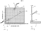
- the probing position setting operation in the eighth embodiment will be described with reference to FIG.
- three contacts 55a to 55c are formed on the surface of the sample 5, and the measurement probe 3a is in contact with the first contact 55a, and the measurement probe 3b is in contact with the third contact 55c. Is shown.
- the measuring probe 3a is moved to the contact 55b, and the electric current is measured while the measuring probe is in contact with the contacts 55b and 55c. It is assumed that characteristic mapping measurement is performed.
- the information processing device 9 sets three-dimensional virtual coordinates 56 in the X, Y, and Z directions, and controls the movement of the measurement probe 3 according to the virtual coordinates 56.
- FIG. 19 shows a state in which virtual coordinates in the X and Y directions and virtual coordinates in the Z direction set by the information processing device 9 are superimposed on the measurement sample 5 for convenience of explanation.
- the virtual coordinates in the X and Y directions can be appropriately set in the SEM image.
- the position coordinates of the first contact 55a are (0, 0)
- the second contact to be the destination is
- the position coordinate of 55b is (7, 5).
- the measurement probe 3 can obtain an appropriate contact by the elastic tip contacting the contact 55 with a predetermined contact pressure. For this reason, in order to move the contact that is in contact, the tip is once moved in the Z direction until it is completely separated from the contact (pulled up), then moved in the (X, Y) direction, and then re-determined at the predetermined contact. It is necessary to move (pull down) in the Z direction so as to come into contact with the destination contact by pressure. For this reason, it is necessary to grasp the amount of drive in the Z direction by the drive device from the state where the contact is properly contacted to the state where the contact is completely separated, and this is specified by the scale of the virtual coordinates in the Z direction.
- the measurement sample 5 is irradiated with an electron beam while the measurement probe 3 is in contact with the contacts 55a and 55c, and the voltage is measured.
- the measurement probe 3a is pulled up in the Z direction while irradiating the electron beam. It is assumed that the measurement voltage becomes 0 at the scale 5 in the Z direction.
- the information processing device 9 can control the contact / non-contact of the measurement probe 3 with the contact 55 by driving the driving device to move the measurement probe 3 up and down by five divisions.
- the scale in the Z direction is equally divided at an arbitrary time based on the drive time of the measuring probe 3 in the Z direction, and this time interval is virtually associated with the scale in the Z direction. This can be achieved by: For example, one graduation in the Z direction can be set as driving the measuring probe 3 in the Z direction for 5 seconds by the driving device.
- the measurer specifies the positions of the plurality of contacts using the virtual coordinates, and the information processing device 9 automatically moves the measurement probe 3 sequentially toward the specified virtual coordinates (X, Y). Then, by bringing the sample into contact with the contact of the measurement sample 5, automatic measurement can be performed. Thereby, the information processing device 9 can display the voltage map images palpated at a plurality of places on the monitor, and can obtain a high measurement throughput.
- the virtual coordinates of the present embodiment can be used not only for setting the probing position but also for setting the electron beam irradiation position.
- FIG. 20 shows a ninth embodiment of the micro device characteristic evaluation apparatus.
- the micro device characteristic evaluation device of the present embodiment has the EBAC control device 21 for acquiring the dynamic EBAC image 62.
- the output of the measurement probe 3 is input to the EBAC controller 21 or the oscilloscope 40 by the switch 60. Further, a voltage amplifier 61 for amplifying the output of the measurement probe 3 is provided between the switch 60 and the EBAC control device 21.
- the measurement sample 5 is irradiated with a pulsed electron beam
- the EBAC controller 21 measures the amount of absorption current in synchronization with the pulsed electron beam
- the information processing device 9 creates an EBAC image based on the measured amount of absorption current. This makes it possible to obtain a dynamic EBAC image that is different from a normal EBAC image and reflects the capacitance component in the measurement sample. Since the EBAC observation can observe a wide range of the sample surface at high speed, the dynamic EBAC observation confirms the approximate abnormal part, and for the electric characteristic mapping measurement that requires time for the measurement processing, the measurement area is narrowed down to a pulse response map image. By creating and analyzing 41, it is possible to efficiently perform abnormality detection and analysis.
- FIG. 21 shows a tenth embodiment of the micro device characteristic evaluation apparatus.
- a voltage signal is applied to the measurement sample 5 from a probe different from a probe for acquiring an electric characteristic map image, and a voltage contrast image 66 obtained at this time and an electric characteristic map (voltage Map) and an image.
- a signal applied to the probe is not limited to a static DC signal, and a signal form such as a dynamic high-frequency signal is not limited.
- the measuring probe 3 is connected to the semiconductor parameter analyzer 8 through the voltage signal applying cable 65 and the measuring cable 13, respectively.
- the voltage signal application cable 65 is merely distinguished from the measurement cable 13 as a function, and is a cable for transmitting an analog signal, and the same cable as the measurement cable 13 may be used.
- a predetermined voltage signal is applied to the measurement sample 5 from the semiconductor parameter analyzer 8 through the measurement probe 3a.
- the information processing device 9 creates a voltage contrast image 66 based on the detection signal from the detector 2.
- the output voltage from the measurement probe 3b is measured by the semiconductor parameter analyzer 8, and a voltage map image is created.
- the measurement method for creating the voltage map image follows the flow of FIG. 2, but in the example of FIG. 21, the purpose is to detect and analyze a defect such as an open fault, and the obtained signal is relatively large.
- the amplification by the differential amplifier as in the device characteristic evaluation apparatus is not performed, and the semiconductor parameter analyzer 8 measures the output voltage from the measurement probe 3b as it is.
- FIGS. An eleventh embodiment of the micro device characteristic evaluation apparatus will be described with reference to FIGS.
- a method of setting virtual coordinates in electrical characteristic mapping measurement will be described.
- the first embodiment, the ninth embodiment, and the tenth embodiment examples in which the cooperative analysis with another evaluation method is performed have been described.
- the second embodiment see FIG.
- the measured values are graphed by designating the region in the electric characteristic map image.
- the region is determined from the SEM image or an image obtained by another evaluation method, for example, the EBAC image. It is also conceivable to use a GUI in which electrical characteristics are specified and measured, and the measured values are graphed.
- the positional relationship between the various electric characteristic map images, the EBAC images, and the voltage contrast images is matched based on the SEM image created by the information processing device 9 based on the detection signal from the detector 2.
- the SEM image is used as a reference because the SEM image shows the structure of the sample in detail, and it is easy to set a reference position for setting virtual coordinates.
- the configuration of the micro device characteristic evaluation device is the same as the configuration of FIG. 1, but a measurement circuit is configured according to the electrical characteristics to be measured and the evaluation method to be applied.
- FIG. 22 is an example of an SEM image 70 acquired by the micro device characteristic evaluation device.
- the field of view of the SEM image is set according to the region to be evaluated.
- two wirings 71 and 72 can be observed on the sample surface. Therefore, three of the corners of the wires 71 and 72 are respectively matched with the first marker 73, the second marker 74, and the third marker 75, and these are registered in the information processing device 9 as reference positions. Note that, as will be described later, at least three markers are required because they serve as references for virtual two-dimensional coordinates, and it is desirable that the positions of the markers be set as far away from each other as possible in the SEM image 70.
- the marker is set using the corner of the wiring as a mark, but the structure of the sample serving as the mark is not limited to the wiring. It is not limited to the structure of the sample, and may be a foreign matter. Further, the shapes of the markers 73 to 75 are not limited to those shown in the drawings.
- virtual coordinates (X, Y) are set.
- the virtual marker 76 is set by the information processing device 9 with the first marker 73 as the origin (0, 0).
- the EBAC image and the electrical characteristic map image are associated with the positional relationship.
- the range in which the electron beam is operated is the same as when the SEM image is created. Can be shared by the EBAC image and the electric characteristic map image as the same.
- virtual values are set based on the imaging conditions (electron beam deflection control amount, magnification change amount, etc.) when the SEM image is obtained and when the EBAC image or the electric characteristic map image is obtained. By performing coordinate conversion of the coordinates, the position of the EBAC image and the position of the electric characteristic map image corresponding to the position specified by the virtual coordinates can be specified for each of the EBAC image and the electric characteristic map image.
- the position specified on the EBAC image is converted into a position on virtual coordinates, and the electric characteristics are calculated based on the virtual coordinates.
- the measured value can be obtained.
- the present invention has been described with reference to a plurality of embodiments.
- the present invention is not limited to the above embodiments, but includes various modifications.
- the above-described embodiments have been described in order to explain the present invention in an easy-to-understand manner, and are not necessarily limited to those having all the configurations described above.
- a part of the configuration of one embodiment can be replaced with the configuration of another embodiment, and the configuration of one embodiment can be added to the configuration of another embodiment.
Landscapes
- Engineering & Computer Science (AREA)
- Physics & Mathematics (AREA)
- General Engineering & Computer Science (AREA)
- General Physics & Mathematics (AREA)
- Microelectronics & Electronic Packaging (AREA)
- Computer Hardware Design (AREA)
- Computer Vision & Pattern Recognition (AREA)
- Health & Medical Sciences (AREA)
- Electromagnetism (AREA)
- Toxicology (AREA)
- Environmental & Geological Engineering (AREA)
- Tests Of Electronic Circuits (AREA)
- Testing Or Measuring Of Semiconductors Or The Like (AREA)
- Crystals, And After-Treatments Of Crystals (AREA)
- Led Devices (AREA)
- Analysing Materials By The Use Of Radiation (AREA)
Abstract
Description
(1)低抵抗性の欠陥に対してEBAC像のコントラストが弱く、欠陥箇所の検知が難しい。例えば、配線不良を例にとると、断線のようなオープン障害の場合は欠陥箇所が高抵抗となり強いコントラストを得られるが、配線ショートの場合はEBAC像に強いコントラストが得られない場合が多く、検知が難しい。
(2)EBAC像の画像処理において、コントラストの黒潰れなど、映像信号のデジタル処理やアンプの特性に起因してEBAC情報の欠損が生じることがある。
Claims (17)
- 試料を載置する試料台と、
前記試料に電子線を照射する電子光学系と、
前記試料に接触される測定探針と、
前記測定探針からの出力を測定する測定器と、
前記試料への前記電子線の照射に応答した前記測定探針からの出力の測定値を取得する情報処理装置とを有し、
前記情報処理装置は、前記試料に対して前記電子線の照射を開始するタイミング及び前記電子線の照射をフリーズするタイミングと、前記電子線が前記試料に照射された状態で前記測定器が前記測定探針からの出力を測定する第1の測定期間と、前記電子線の照射がフリーズされた後に前記測定器が前記測定探針からの出力を測定する第2の測定期間とを設定し、
前記試料への前記電子線の照射に応答した前記測定探針からの出力の測定値を、前記第1の測定期間に測定された第1の測定値と前記第2の測定期間に測定された第2の測定値との差から求める半導体検査装置。 - 請求項1において、
前記情報処理装置は、前記試料に対して前記電子線を照射したときの前記測定探針からの出力の時間変化を検出し、前記第1の測定期間及び前記第2の測定期間が前記時間変化の少ない時間帯に含まれるように設定する半導体検査装置。 - 請求項2において、
前記第1の測定値は、前記測定器が前記第1の測定期間において測定した測定値を積算処理した値であり、前記第2の測定値は、前記測定器が前記第2の測定期間において測定した測定値を積算処理した値である半導体検査装置。 - 請求項3において、
前記測定器は、前記電子線の照射に応答して前記測定探針に生じる電圧信号を測定する半導体検査装置。 - 請求項3において、
前記試料に接触される第1の測定探針及び第2の測定探針と、
前記第1の測定探針からの出力が第1の入力端子に接続され、前記第2の測定探針からの出力が第2の入力端子に接続される差動アンプとを有し、
前記測定器は、前記差動アンプから出力される電圧信号を測定する半導体検査装置。 - 請求項5において、
前記情報処理装置は、前記差動アンプのゲインを制御する半導体検査装置。 - 請求項3において、
前記測定器は、前記電子線の照射に応答して前記測定探針に生じる電流信号を測定する半導体検査装置。 - 請求項3において、
前記電子光学系は前記試料上を2次元に走査し、
前記情報処理装置は、前記電子線の照射に応答した前記測定探針からの出力の測定値を、前記電子線の照射位置と対応付けて記憶する半導体検査装置。 - 請求項8において、
前記情報処理装置は、前記電子線の照射位置に対応する画素の画素値を、前記電子線の照射に応答した前記測定探針からの出力の測定値に基づき決定した数値マッピング画像を作成する半導体検査装置。 - 請求項8において、
前記電子線と前記試料との相互作用により放出される信号電子を検出する検出器を有し、
前記情報処理装置は、前記検出器から検出された信号からSEM像を作成し、前記SEM像に基づき仮想座標を設定する半導体検査装置。 - 請求項10において、
前記情報処理装置は、前記仮想座標により指定された位置に前記測定探針を移動させる半導体検査装置。 - 試料を載置する試料台と、
前記試料に電子線を照射する電子光学系と、
前記試料に接触される測定探針と、
前記測定探針からの出力を測定する測定器と、
前記電子線と前記試料との相互作用により放出される信号電子を検出する検出器と、
前記試料への前記電子線の照射に応答した前記測定探針からの出力の測定値を取得する情報処理装置とを有し、
前記電子光学系は第1の撮像条件により前記試料上を2次元に走査し、前記情報処理装置は、前記検出器から検出された信号からSEM像を作成し、前記SEM像に基づき仮想座標を設定し、
前記電子光学系は第2の撮像条件により前記試料上を2次元に走査し、前記情報処理装置は、前記測定器により測定された前記測定探針からの出力の測定値に基づき電気特性マップ像を作成し、
前記情報処理装置は、前記仮想座標を前記第1の撮像条件及び前記第2の撮像条件に基づき座標変換することにより、前記仮想座標により指定された位置を前記電気特性マップ像上で特定する半導体検査装置。 - 請求項12において、
前記情報処理装置は、前記電気特性マップ像の画素値を、前記電気特性マップ像の画素に対応する位置への前記電子線の照射に応答した前記測定探針からの出力の測定値に基づき決定する半導体検査装置。 - 請求項12において、
前記電子線の照射に応答した前記測定探針からの出力より、前記電子線の照射位置における吸収電流量を示す信号を出力するEBAC(Electron Beam Absorbed Current)制御装置を有し、
前記電子光学系は第3の撮像条件により前記試料上を2次元に走査し、前記情報処理装置は、前記EBAC制御装置が出力した信号からEBAC像を作成し、前記仮想座標を前記第1の撮像条件及び前記第3の撮像条件に基づき座標変換することにより、前記EBAC像上の位置を前記仮想座標上の位置に変換する半導体検査装置。 - 請求項12において、
前記測定器が測定する前記測定探針からの出力の測定値は電圧値または電流値である半導体検査装置。 - 請求項12において、
前記電子光学系は、前記試料にパルス電子線を照射し、
前記測定器が測定する前記測定探針からの出力の測定値はパルス応答特性である半導体検査装置。 - 請求項16において、
前記パルス電子線の照射に応答した前記測定探針からの出力より、前記パルス電子線と同期して、前記パルス電子線の照射位置における吸収電流量を示す信号を出力するEBAC(Electron Beam Absorbed Current)制御装置を有し、
前記電子光学系は第4の撮像条件により前記試料上を2次元に走査し、前記情報処理装置は、前記EBAC制御装置が出力した信号から動的EBAC像を作成し、前記仮想座標を前記第1の撮像条件及び前記第4の撮像条件に基づき座標変換することにより、前記動的EBAC像上の位置を前記仮想座標上の位置に変換する半導体検査装置。
Priority Applications (6)
| Application Number | Priority Date | Filing Date | Title |
|---|---|---|---|
| US17/256,083 US11719746B2 (en) | 2018-06-28 | 2018-06-28 | Semiconductor inspection device |
| JP2020526821A JP7159312B2 (ja) | 2018-06-28 | 2018-06-28 | 半導体検査装置 |
| PCT/JP2018/024678 WO2020003458A1 (ja) | 2018-06-28 | 2018-06-28 | 半導体検査装置 |
| CN201880095003.4A CN112313782B (zh) | 2018-06-28 | 2018-06-28 | 半导体检查装置 |
| KR1020207036872A KR102440165B1 (ko) | 2018-06-28 | 2018-06-28 | 반도체 검사 장치 |
| TW108120621A TWI716901B (zh) | 2018-06-28 | 2019-06-14 | 半導體檢查裝置 |
Applications Claiming Priority (1)
| Application Number | Priority Date | Filing Date | Title |
|---|---|---|---|
| PCT/JP2018/024678 WO2020003458A1 (ja) | 2018-06-28 | 2018-06-28 | 半導体検査装置 |
Publications (1)
| Publication Number | Publication Date |
|---|---|
| WO2020003458A1 true WO2020003458A1 (ja) | 2020-01-02 |
Family
ID=68986750
Family Applications (1)
| Application Number | Title | Priority Date | Filing Date |
|---|---|---|---|
| PCT/JP2018/024678 Ceased WO2020003458A1 (ja) | 2018-06-28 | 2018-06-28 | 半導体検査装置 |
Country Status (6)
| Country | Link |
|---|---|
| US (1) | US11719746B2 (ja) |
| JP (1) | JP7159312B2 (ja) |
| KR (1) | KR102440165B1 (ja) |
| CN (1) | CN112313782B (ja) |
| TW (1) | TWI716901B (ja) |
| WO (1) | WO2020003458A1 (ja) |
Cited By (4)
| Publication number | Priority date | Publication date | Assignee | Title |
|---|---|---|---|---|
| US20210270891A1 (en) * | 2018-06-28 | 2021-09-02 | Hitachi High-Tech Corporation | Semiconductor Inspection Device |
| CN114170092A (zh) * | 2020-09-10 | 2022-03-11 | Imec 非营利协会 | 用于对电子显微镜图像进行去噪的方法 |
| JPWO2022219695A1 (ja) * | 2021-04-13 | 2022-10-20 | ||
| JP2026062066A (ja) * | 2024-09-30 | 2026-04-09 | 東芝情報システム株式会社 | 半導体検査装置及び半導体検査方法 |
Families Citing this family (8)
| Publication number | Priority date | Publication date | Assignee | Title |
|---|---|---|---|---|
| US11410830B1 (en) * | 2019-03-23 | 2022-08-09 | Kla Corporation | Defect inspection and review using transmissive current image of charged particle beam system |
| TWI741747B (zh) * | 2020-08-20 | 2021-10-01 | 鴻勁精密股份有限公司 | 作業裝置之壓接機構 |
| JP7507838B2 (ja) | 2021-11-30 | 2024-06-28 | イノヴェータム・インストゥルメンツ・インコーポレイテッド | 荷電粒子ビームを使用するプローブ先端のx-yロケーションの識別 |
| TWI799024B (zh) * | 2021-12-22 | 2023-04-11 | 技嘉科技股份有限公司 | 自動量測訊號的控制系統與方法 |
| US12306241B2 (en) | 2022-02-14 | 2025-05-20 | Innovatum Instruments Inc. | Automated probe landing |
| JP2025522959A (ja) * | 2022-07-08 | 2025-07-17 | アプライド マテリアルズ インコーポレイテッド | パッケージング基板を試験するための方法およびパッケージング基板を試験するための装置 |
| WO2024257200A1 (ja) * | 2023-06-13 | 2024-12-19 | 株式会社日立ハイテク | 電子線応用装置及び時定数計測方法 |
| CN119199225A (zh) * | 2024-09-20 | 2024-12-27 | 无锡卓海科技股份有限公司 | 一种可拍照记录的万用表及电路板测试系统和方法 |
Citations (13)
| Publication number | Priority date | Publication date | Assignee | Title |
|---|---|---|---|---|
| JPH02157665A (ja) * | 1988-12-09 | 1990-06-18 | Fujitsu Ltd | 電子ビームテスタ |
| JP2001156136A (ja) * | 1999-11-30 | 2001-06-08 | Jeol Ltd | 荷電粒子ビームを用いたホールの検査方法 |
| JP2002176088A (ja) * | 2000-12-08 | 2002-06-21 | Nec Corp | 半導体デバイス検査装置 |
| JP2002310954A (ja) * | 2001-04-18 | 2002-10-23 | Shimadzu Corp | 試料解析装置 |
| JP2004146802A (ja) * | 2002-10-02 | 2004-05-20 | Jeol Ltd | 半導体ウェハ試料の検査方法および装置 |
| JP2004296771A (ja) * | 2003-03-27 | 2004-10-21 | Renesas Technology Corp | 半導体検査装置及び検査方法 |
| JP2005210067A (ja) * | 2003-12-24 | 2005-08-04 | Hitachi High-Technologies Corp | プローブナビゲーション方法及び装置並びに不良検査装置 |
| JP2008041757A (ja) * | 2006-08-02 | 2008-02-21 | Nec Electronics Corp | 半導体検査装置および半導体検査方法 |
| JP2008166702A (ja) * | 2006-12-06 | 2008-07-17 | Jeol Ltd | 荷電粒子ビーム装置 |
| JP2008204775A (ja) * | 2007-02-20 | 2008-09-04 | Jeol Ltd | 荷電粒子ビーム装置 |
| JP2009117774A (ja) * | 2007-11-09 | 2009-05-28 | Renesas Technology Corp | 半導体装置の不良解析方法および不良解析装置 |
| JP2011185633A (ja) * | 2010-03-05 | 2011-09-22 | Toshiba Corp | 電子部品の検査方法及び検査装置 |
| JP2013187510A (ja) * | 2012-03-09 | 2013-09-19 | Hitachi High-Technologies Corp | 半導体検査装置および半導体検査方法 |
Family Cites Families (35)
| Publication number | Priority date | Publication date | Assignee | Title |
|---|---|---|---|---|
| US4812623A (en) * | 1985-02-05 | 1989-03-14 | D. H. Haden Limited | Electrical apparatus |
| IN165839B (ja) * | 1985-02-05 | 1990-01-20 | Haden D H Ltd | |
| KR100200215B1 (ko) * | 1996-04-08 | 1999-06-15 | 윤종용 | 상관 신경 회로망을 이용한 납땜 검사 장치 및방법 |
| CN100382272C (zh) * | 1999-11-05 | 2008-04-16 | 拓普康株式会社 | 半导体器件检查装置 |
| JP3749107B2 (ja) * | 1999-11-05 | 2006-02-22 | ファブソリューション株式会社 | 半導体デバイス検査装置 |
| JP4767650B2 (ja) * | 1999-11-05 | 2011-09-07 | 株式会社トプコン | 半導体デバイス検査装置 |
| JP4312910B2 (ja) * | 1999-12-02 | 2009-08-12 | 株式会社日立製作所 | レビューsem |
| JP3955445B2 (ja) * | 2001-06-11 | 2007-08-08 | 株式会社ルネサステクノロジ | 半導体装置の検査方法及び試料検査装置 |
| US6819117B2 (en) | 2002-01-30 | 2004-11-16 | Credence Systems Corporation | PICA system timing measurement & calibration |
| JP2004340652A (ja) | 2003-05-14 | 2004-12-02 | Hitachi Ltd | 欠陥検査装置および陽電子線応用装置 |
| JP4629493B2 (ja) * | 2005-05-11 | 2011-02-09 | ルネサスエレクトロニクス株式会社 | 半導体装置の検査方法 |
| TWI512304B (zh) | 2005-09-13 | 2015-12-11 | 荏原製作所股份有限公司 | 半導體裝置及其檢查方法 |
| JP4467588B2 (ja) | 2007-02-28 | 2010-05-26 | 株式会社日立ハイテクノロジーズ | 試料検査装置及び吸収電流像の作成方法 |
| JP5352135B2 (ja) | 2007-06-25 | 2013-11-27 | 株式会社日立ハイテクノロジーズ | 検査装置及び検査方法 |
| JP2009141090A (ja) * | 2007-12-06 | 2009-06-25 | Renesas Technology Corp | 走査型電子顕微鏡 |
| JP2010040803A (ja) * | 2008-08-06 | 2010-02-18 | Hitachi High-Technologies Corp | 電子ビームを用いた半導体検査装置 |
| JP2010135684A (ja) | 2008-12-08 | 2010-06-17 | Renesas Technology Corp | 電子ビーム吸収電流解析方法及び電子ビーム吸収電流解析器 |
| WO2011155044A1 (ja) * | 2010-06-10 | 2011-12-15 | 株式会社島津製作所 | Tftアレイ検査の電子線走査方法およびtftアレイ検査装置 |
| JP5684612B2 (ja) * | 2011-03-09 | 2015-03-18 | 株式会社日立ハイテクサイエンス | X線分析装置 |
| WO2013012616A2 (en) | 2011-07-15 | 2013-01-24 | Orbotech Ltd. | Electrical inspection of electronic devices using electron-beam induced plasma probes |
| JP5983275B2 (ja) * | 2012-10-09 | 2016-08-31 | 富士通株式会社 | 検査装置および検査方法 |
| JP2014143348A (ja) * | 2013-01-25 | 2014-08-07 | Renesas Electronics Corp | 半導体装置の不良解析方法、および不良解析装置 |
| WO2014119676A1 (ja) * | 2013-02-01 | 2014-08-07 | 浜松ホトニクス株式会社 | 半導体デバイス検査装置及び半導体デバイス検査方法 |
| JP6117625B2 (ja) * | 2013-06-07 | 2017-04-19 | 三星電子株式会社Samsung Electronics Co.,Ltd. | 電子線検査装置及び電子線検査方法 |
| JP5453664B1 (ja) * | 2013-07-16 | 2014-03-26 | Wafer Integration株式会社 | 自己検知型カンチレバーを用いた走査型探針顕微鏡式プローバ |
| JP6283501B2 (ja) * | 2013-11-12 | 2018-02-21 | 浜松ホトニクス株式会社 | 周波数解析装置及び周波数解析方法 |
| WO2016002003A1 (ja) | 2014-07-01 | 2016-01-07 | 株式会社日立ハイテクノロジーズ | 基板検査装置及び方法 |
| KR102104059B1 (ko) * | 2014-07-31 | 2020-04-23 | 삼성전자 주식회사 | 전도성 원자힘 현미경 장치 및 전도성 원자힘 현미경 장치의 동작 방법 |
| JP6520356B2 (ja) * | 2015-04-28 | 2019-05-29 | 新東工業株式会社 | 検査装置および検査方法 |
| KR102234251B1 (ko) * | 2015-07-29 | 2021-04-01 | 주식회사 히타치하이테크 | 동적인 응답 해석 프로버 장치 |
| CN107923939B (zh) * | 2015-09-02 | 2021-11-19 | 株式会社日立高新技术 | 电路检查方法以及样品检查装置 |
| JP6865044B2 (ja) * | 2017-01-19 | 2021-04-28 | 浜松ホトニクス株式会社 | 検査方法、検査装置、及びマーキング形成方法 |
| US20190152595A1 (en) * | 2017-11-17 | 2019-05-23 | Bigfoot Technologies Inc. | Apparatus for Sustained Surveillance and Deterrence with Unmanned Aerial Vehicles (UAV) |
| WO2020003458A1 (ja) * | 2018-06-28 | 2020-01-02 | 株式会社日立ハイテクノロジーズ | 半導体検査装置 |
| CN117280224A (zh) * | 2021-05-21 | 2023-12-22 | 株式会社日立高新技术 | 试样检查装置 |
-
2018
- 2018-06-28 WO PCT/JP2018/024678 patent/WO2020003458A1/ja not_active Ceased
- 2018-06-28 KR KR1020207036872A patent/KR102440165B1/ko active Active
- 2018-06-28 US US17/256,083 patent/US11719746B2/en active Active
- 2018-06-28 CN CN201880095003.4A patent/CN112313782B/zh active Active
- 2018-06-28 JP JP2020526821A patent/JP7159312B2/ja active Active
-
2019
- 2019-06-14 TW TW108120621A patent/TWI716901B/zh active
Patent Citations (13)
| Publication number | Priority date | Publication date | Assignee | Title |
|---|---|---|---|---|
| JPH02157665A (ja) * | 1988-12-09 | 1990-06-18 | Fujitsu Ltd | 電子ビームテスタ |
| JP2001156136A (ja) * | 1999-11-30 | 2001-06-08 | Jeol Ltd | 荷電粒子ビームを用いたホールの検査方法 |
| JP2002176088A (ja) * | 2000-12-08 | 2002-06-21 | Nec Corp | 半導体デバイス検査装置 |
| JP2002310954A (ja) * | 2001-04-18 | 2002-10-23 | Shimadzu Corp | 試料解析装置 |
| JP2004146802A (ja) * | 2002-10-02 | 2004-05-20 | Jeol Ltd | 半導体ウェハ試料の検査方法および装置 |
| JP2004296771A (ja) * | 2003-03-27 | 2004-10-21 | Renesas Technology Corp | 半導体検査装置及び検査方法 |
| JP2005210067A (ja) * | 2003-12-24 | 2005-08-04 | Hitachi High-Technologies Corp | プローブナビゲーション方法及び装置並びに不良検査装置 |
| JP2008041757A (ja) * | 2006-08-02 | 2008-02-21 | Nec Electronics Corp | 半導体検査装置および半導体検査方法 |
| JP2008166702A (ja) * | 2006-12-06 | 2008-07-17 | Jeol Ltd | 荷電粒子ビーム装置 |
| JP2008204775A (ja) * | 2007-02-20 | 2008-09-04 | Jeol Ltd | 荷電粒子ビーム装置 |
| JP2009117774A (ja) * | 2007-11-09 | 2009-05-28 | Renesas Technology Corp | 半導体装置の不良解析方法および不良解析装置 |
| JP2011185633A (ja) * | 2010-03-05 | 2011-09-22 | Toshiba Corp | 電子部品の検査方法及び検査装置 |
| JP2013187510A (ja) * | 2012-03-09 | 2013-09-19 | Hitachi High-Technologies Corp | 半導体検査装置および半導体検査方法 |
Cited By (11)
| Publication number | Priority date | Publication date | Assignee | Title |
|---|---|---|---|---|
| US20210270891A1 (en) * | 2018-06-28 | 2021-09-02 | Hitachi High-Tech Corporation | Semiconductor Inspection Device |
| US11719746B2 (en) * | 2018-06-28 | 2023-08-08 | Hitachi High-Tech Corporation | Semiconductor inspection device |
| CN114170092A (zh) * | 2020-09-10 | 2022-03-11 | Imec 非营利协会 | 用于对电子显微镜图像进行去噪的方法 |
| EP4231227A3 (en) * | 2020-09-10 | 2023-11-15 | Imec VZW | Method for denoising an electron microscope image |
| US12243193B2 (en) | 2020-09-10 | 2025-03-04 | Imec Vzw | Method for de-noising an electron microscope image |
| CN114170092B (zh) * | 2020-09-10 | 2025-11-28 | Imec非营利协会 | 用于对电子显微镜图像进行去噪的方法 |
| JPWO2022219695A1 (ja) * | 2021-04-13 | 2022-10-20 | ||
| WO2022219695A1 (ja) * | 2021-04-13 | 2022-10-20 | 株式会社日立ハイテク | 試料検査装置、検査システム、薄片試料作製装置および試料の検査方法 |
| JP7538339B2 (ja) | 2021-04-13 | 2024-08-21 | 株式会社日立ハイテク | 試料検査装置、検査システム、薄片試料作製装置および試料の検査方法 |
| US12562335B2 (en) | 2021-04-13 | 2026-02-24 | Hitachi High-Tech Corporation | Sample inspection apparatus, inspection system, thin piece sample fabrication apparatus, and method for inspecting sample |
| JP2026062066A (ja) * | 2024-09-30 | 2026-04-09 | 東芝情報システム株式会社 | 半導体検査装置及び半導体検査方法 |
Also Published As
| Publication number | Publication date |
|---|---|
| JPWO2020003458A1 (ja) | 2021-07-08 |
| US11719746B2 (en) | 2023-08-08 |
| TW202001250A (zh) | 2020-01-01 |
| KR102440165B1 (ko) | 2022-09-06 |
| CN112313782A (zh) | 2021-02-02 |
| US20210270891A1 (en) | 2021-09-02 |
| CN112313782B (zh) | 2023-10-13 |
| KR20210013158A (ko) | 2021-02-03 |
| JP7159312B2 (ja) | 2022-10-24 |
| TWI716901B (zh) | 2021-01-21 |
Similar Documents
| Publication | Publication Date | Title |
|---|---|---|
| JP7159312B2 (ja) | 半導体検査装置 | |
| TW201704766A (zh) | 加熱粒子束以識別缺陷 | |
| JP2006105960A (ja) | 試料検査方法及び試料検査装置 | |
| JP3776902B2 (ja) | 基板検査装置、基板検査方法、プログラムおよび半導体装置の製造方法 | |
| US10712384B2 (en) | Circuit inspection method and sample inspection apparatus | |
| JP2008166702A (ja) | 荷電粒子ビーム装置 | |
| KR102707286B1 (ko) | 시료 검사 장치 | |
| JP2004296771A (ja) | 半導体検査装置及び検査方法 | |
| JP5296751B2 (ja) | 試料検査装置及び吸収電流像の作成方法 | |
| JP4290316B2 (ja) | 配線ショート箇所の検査方法及び検査装置 | |
| JP7538339B2 (ja) | 試料検査装置、検査システム、薄片試料作製装置および試料の検査方法 | |
| KR102189053B1 (ko) | 동적인 응답 해석 프로버 장치 | |
| JP2008210987A (ja) | 半導体素子の解析装置及びその解析方法 | |
| Jatzkowski et al. | Localization of weak points in thin dielectric layers by Electron Beam Absorbed Current (EBAC) Imaging | |
| JP2011043346A (ja) | 半導体デバイス検査方法及び装置 | |
| Smith et al. | Combining a Nanoprobing Setup with PFIB Sample Deprocessing | |
| JP2010135679A (ja) | 半導体検査装置及び検査方法 | |
| US20130088585A1 (en) | Surface imaging with materials identified by color | |
| JP2010123934A (ja) | 半導体検査装置のデータ処理方法とデータ表示方法と半導体検査装置 |
Legal Events
| Date | Code | Title | Description |
|---|---|---|---|
| 121 | Ep: the epo has been informed by wipo that ep was designated in this application |
Ref document number: 18924255 Country of ref document: EP Kind code of ref document: A1 |
|
| ENP | Entry into the national phase |
Ref document number: 2020526821 Country of ref document: JP Kind code of ref document: A Ref document number: 20207036872 Country of ref document: KR Kind code of ref document: A |
|
| NENP | Non-entry into the national phase |
Ref country code: DE |
|
| 122 | Ep: pct application non-entry in european phase |
Ref document number: 18924255 Country of ref document: EP Kind code of ref document: A1 |