WO2019244697A1 - プラズマ処理方法及びプラズマ処理装置 - Google Patents
プラズマ処理方法及びプラズマ処理装置 Download PDFInfo
- Publication number
- WO2019244697A1 WO2019244697A1 PCT/JP2019/022952 JP2019022952W WO2019244697A1 WO 2019244697 A1 WO2019244697 A1 WO 2019244697A1 JP 2019022952 W JP2019022952 W JP 2019022952W WO 2019244697 A1 WO2019244697 A1 WO 2019244697A1
- Authority
- WO
- WIPO (PCT)
- Prior art keywords
- frequency power
- period
- film
- supplied
- plasma processing
- Prior art date
- Legal status (The legal status is an assumption and is not a legal conclusion. Google has not performed a legal analysis and makes no representation as to the accuracy of the status listed.)
- Ceased
Links
Images


Classifications
-
- H—ELECTRICITY
- H01—ELECTRIC ELEMENTS
- H01J—ELECTRIC DISCHARGE TUBES OR DISCHARGE LAMPS
- H01J37/00—Discharge tubes with provision for introducing objects or material to be exposed to the discharge, e.g. for the purpose of examination or processing thereof
- H01J37/32—Gas-filled discharge tubes
- H01J37/32009—Arrangements for generation of plasma specially adapted for examination or treatment of objects, e.g. plasma sources
- H01J37/32082—Radio frequency generated discharge
- H01J37/32174—Circuits specially adapted for controlling the RF discharge
-
- H—ELECTRICITY
- H01—ELECTRIC ELEMENTS
- H01J—ELECTRIC DISCHARGE TUBES OR DISCHARGE LAMPS
- H01J37/00—Discharge tubes with provision for introducing objects or material to be exposed to the discharge, e.g. for the purpose of examination or processing thereof
- H01J37/32—Gas-filled discharge tubes
- H01J37/32009—Arrangements for generation of plasma specially adapted for examination or treatment of objects, e.g. plasma sources
- H01J37/32082—Radio frequency generated discharge
- H01J37/32137—Radio frequency generated discharge controlling of the discharge by modulation of energy
- H01J37/32155—Frequency modulation
- H01J37/32165—Plural frequencies
-
- H—ELECTRICITY
- H10—SEMICONDUCTOR DEVICES; ELECTRIC SOLID-STATE DEVICES NOT OTHERWISE PROVIDED FOR
- H10P—GENERIC PROCESSES OR APPARATUS FOR THE MANUFACTURE OR TREATMENT OF DEVICES COVERED BY CLASS H10
- H10P72/00—Handling or holding of wafers, substrates or devices during manufacture or treatment thereof
- H10P72/04—Apparatus for manufacture or treatment
- H10P72/0402—Apparatus for fluid treatment
- H10P72/0418—Apparatus for fluid treatment for etching
- H10P72/0421—Apparatus for fluid treatment for etching for drying etching
-
- H—ELECTRICITY
- H05—ELECTRIC TECHNIQUES NOT OTHERWISE PROVIDED FOR
- H05H—PLASMA TECHNIQUE; PRODUCTION OF ACCELERATED ELECTRICALLY-CHARGED PARTICLES OR OF NEUTRONS; PRODUCTION OR ACCELERATION OF NEUTRAL MOLECULAR OR ATOMIC BEAMS
- H05H1/00—Generating plasma; Handling plasma
- H05H1/24—Generating plasma
- H05H1/46—Generating plasma using applied electromagnetic fields, e.g. high frequency or microwave energy
-
- H—ELECTRICITY
- H01—ELECTRIC ELEMENTS
- H01J—ELECTRIC DISCHARGE TUBES OR DISCHARGE LAMPS
- H01J37/00—Discharge tubes with provision for introducing objects or material to be exposed to the discharge, e.g. for the purpose of examination or processing thereof
- H01J37/32—Gas-filled discharge tubes
- H01J37/32009—Arrangements for generation of plasma specially adapted for examination or treatment of objects, e.g. plasma sources
- H01J37/32082—Radio frequency generated discharge
- H01J37/32137—Radio frequency generated discharge controlling of the discharge by modulation of energy
- H01J37/32146—Amplitude modulation, includes pulsing
-
- H—ELECTRICITY
- H01—ELECTRIC ELEMENTS
- H01J—ELECTRIC DISCHARGE TUBES OR DISCHARGE LAMPS
- H01J37/00—Discharge tubes with provision for introducing objects or material to be exposed to the discharge, e.g. for the purpose of examination or processing thereof
- H01J37/32—Gas-filled discharge tubes
- H01J37/32009—Arrangements for generation of plasma specially adapted for examination or treatment of objects, e.g. plasma sources
- H01J37/32082—Radio frequency generated discharge
- H01J37/32174—Circuits specially adapted for controlling the RF discharge
- H01J37/32183—Matching circuits
-
- H—ELECTRICITY
- H01—ELECTRIC ELEMENTS
- H01J—ELECTRIC DISCHARGE TUBES OR DISCHARGE LAMPS
- H01J37/00—Discharge tubes with provision for introducing objects or material to be exposed to the discharge, e.g. for the purpose of examination or processing thereof
- H01J37/32—Gas-filled discharge tubes
- H01J37/32431—Constructional details of the reactor
- H01J37/32532—Electrodes
- H01J37/32577—Electrical connecting means
-
- H—ELECTRICITY
- H01—ELECTRIC ELEMENTS
- H01J—ELECTRIC DISCHARGE TUBES OR DISCHARGE LAMPS
- H01J37/00—Discharge tubes with provision for introducing objects or material to be exposed to the discharge, e.g. for the purpose of examination or processing thereof
- H01J37/32—Gas-filled discharge tubes
- H01J37/32431—Constructional details of the reactor
- H01J37/32697—Electrostatic control
- H01J37/32706—Polarising the substrate
-
- H—ELECTRICITY
- H05—ELECTRIC TECHNIQUES NOT OTHERWISE PROVIDED FOR
- H05H—PLASMA TECHNIQUE; PRODUCTION OF ACCELERATED ELECTRICALLY-CHARGED PARTICLES OR OF NEUTRONS; PRODUCTION OR ACCELERATION OF NEUTRAL MOLECULAR OR ATOMIC BEAMS
- H05H1/00—Generating plasma; Handling plasma
- H05H1/24—Generating plasma
-
- H—ELECTRICITY
- H10—SEMICONDUCTOR DEVICES; ELECTRIC SOLID-STATE DEVICES NOT OTHERWISE PROVIDED FOR
- H10P—GENERIC PROCESSES OR APPARATUS FOR THE MANUFACTURE OR TREATMENT OF DEVICES COVERED BY CLASS H10
- H10P14/00—Formation of materials, e.g. in the shape of layers or pillars
- H10P14/60—Formation of materials, e.g. in the shape of layers or pillars of insulating materials
- H10P14/61—Formation of materials, e.g. in the shape of layers or pillars of insulating materials using masks
-
- H—ELECTRICITY
- H10—SEMICONDUCTOR DEVICES; ELECTRIC SOLID-STATE DEVICES NOT OTHERWISE PROVIDED FOR
- H10P—GENERIC PROCESSES OR APPARATUS FOR THE MANUFACTURE OR TREATMENT OF DEVICES COVERED BY CLASS H10
- H10P50/00—Etching of wafers, substrates or parts of devices
- H10P50/20—Dry etching; Plasma etching; Reactive-ion etching
- H10P50/24—Dry etching; Plasma etching; Reactive-ion etching of semiconductor materials
- H10P50/242—Dry etching; Plasma etching; Reactive-ion etching of semiconductor materials of Group IV materials
-
- H—ELECTRICITY
- H10—SEMICONDUCTOR DEVICES; ELECTRIC SOLID-STATE DEVICES NOT OTHERWISE PROVIDED FOR
- H10P—GENERIC PROCESSES OR APPARATUS FOR THE MANUFACTURE OR TREATMENT OF DEVICES COVERED BY CLASS H10
- H10P50/00—Etching of wafers, substrates or parts of devices
- H10P50/20—Dry etching; Plasma etching; Reactive-ion etching
- H10P50/26—Dry etching; Plasma etching; Reactive-ion etching of conductive or resistive materials
- H10P50/264—Dry etching; Plasma etching; Reactive-ion etching of conductive or resistive materials by chemical means
- H10P50/266—Dry etching; Plasma etching; Reactive-ion etching of conductive or resistive materials by chemical means by vapour etching only
- H10P50/267—Dry etching; Plasma etching; Reactive-ion etching of conductive or resistive materials by chemical means by vapour etching only using plasmas
-
- H—ELECTRICITY
- H10—SEMICONDUCTOR DEVICES; ELECTRIC SOLID-STATE DEVICES NOT OTHERWISE PROVIDED FOR
- H10P—GENERIC PROCESSES OR APPARATUS FOR THE MANUFACTURE OR TREATMENT OF DEVICES COVERED BY CLASS H10
- H10P50/00—Etching of wafers, substrates or parts of devices
- H10P50/20—Dry etching; Plasma etching; Reactive-ion etching
- H10P50/28—Dry etching; Plasma etching; Reactive-ion etching of insulating materials
- H10P50/282—Dry etching; Plasma etching; Reactive-ion etching of insulating materials of inorganic materials
- H10P50/283—Dry etching; Plasma etching; Reactive-ion etching of insulating materials of inorganic materials by chemical means
-
- H—ELECTRICITY
- H01—ELECTRIC ELEMENTS
- H01J—ELECTRIC DISCHARGE TUBES OR DISCHARGE LAMPS
- H01J2237/00—Discharge tubes exposing object to beam, e.g. for analysis treatment, etching, imaging
- H01J2237/32—Processing objects by plasma generation
- H01J2237/33—Processing objects by plasma generation characterised by the type of processing
- H01J2237/334—Etching
- H01J2237/3341—Reactive etching
-
- H—ELECTRICITY
- H05—ELECTRIC TECHNIQUES NOT OTHERWISE PROVIDED FOR
- H05H—PLASMA TECHNIQUE; PRODUCTION OF ACCELERATED ELECTRICALLY-CHARGED PARTICLES OR OF NEUTRONS; PRODUCTION OR ACCELERATION OF NEUTRAL MOLECULAR OR ATOMIC BEAMS
- H05H2245/00—Applications of plasma devices
- H05H2245/40—Surface treatments
- H05H2245/42—Coating or etching of large items
Definitions
- the exemplary embodiment of the present disclosure relates to a plasma processing method and a plasma processing apparatus.
- plasma processing is performed using a plasma processing apparatus.
- the plasma processing apparatus includes a chamber and a substrate support.
- the substrate support includes a lower electrode and is provided in the chamber.
- high-frequency power is supplied to excite a gas in a chamber, and plasma is generated from the gas.
- another high-frequency power can be supplied to the lower electrode.
- Another high frequency power has a lower frequency than the frequency of the high frequency power for plasma generation. That is, another high frequency power is a bias high frequency power.
- the bias radio frequency power is used to adjust the energy of ions that collide with a substrate provided on a substrate support. The energy of the ions impinging on the substrate will be higher if a bias RF power having a higher power level is supplied to the lower electrode. On the other hand, the energy of the ions colliding with the substrate will be lower if a bias RF power having a lower power level is supplied to the lower electrode.
- Patent Document 1 describes a plasma treatment for etching a silicon nitride film.
- the power level of the bias high-frequency power is set to a high level during the etching of the silicon nitride film.
- the power level of the bias high-frequency power becomes high. And alternately to a lower level.
- a plasma processing method includes performing a first plasma process in a chamber during a first time period, and performing a second plasma process in the chamber during a second time period after the first time period or subsequent to the first time period. Performing a process.
- the first high frequency power is continuously supplied to the lower electrode of the substrate support in the step of performing the first plasma processing and the step of performing the second plasma processing.
- the first high frequency power has a first frequency.
- the substrate support is provided in the chamber.
- the second high-frequency power is supplied as pulsed high-frequency power in a first partial period of the first period and in a second partial period of the second period.
- the second high frequency power is a high frequency power for plasma generation having a second frequency higher than the first frequency.
- the first partial period is a partial period in each cycle of the first high-frequency power.
- the second partial period is a partial period in each cycle of the first high-frequency power and is different from the first partial period.
- the second high-frequency power is supplied as one of a pulsed high-frequency power and a continuous high-frequency power in each cycle of the first high-frequency power in the first period, and Within each period of the first high-frequency power in the period, it is supplied as the other high-frequency power.
- the second high-frequency power is supplied as pulsed high-frequency power in each cycle of the first high-frequency power in the first period, and is not supplied in the second period.
- the plasma processing method it is possible to rapidly change the energy of ions traveling toward the substrate support.
- FIG. 3 is a flowchart of a plasma processing method according to one exemplary embodiment.
- FIG. 1 schematically illustrates a plasma processing apparatus according to one exemplary embodiment.
- FIG. 4 is a diagram schematically illustrating a plasma processing apparatus according to another exemplary embodiment.
- FIG. 4A is a partially enlarged cross-sectional view of an example substrate
- FIGS. 4B and 4C are diagrams of an example substrate in a state after execution of each of a plurality of steps of the method MT1. It is a partially expanded sectional view.
- 6 is an example timing chart related to the method MT1. It is a timing chart which shows an example of 2nd high frequency power as continuous high frequency power.
- 5 is a flowchart of a plasma processing method according to another exemplary embodiment.
- FIG. 1 schematically illustrates a plasma processing apparatus according to one exemplary embodiment.
- FIG. 4 is a diagram schematically illustrating a plasma processing apparatus according to another exemplary embodiment.
- FIG. 4A is a partially enlarged
- FIG. 8A is a partially enlarged cross-sectional view of an example of a substrate
- FIGS. 8B to 8E are examples of a state after execution of each of the plurality of steps of the method MT2.
- FIG. 4 is a partially enlarged cross-sectional view of a substrate.
- FIG. 9 is a flowchart of a plasma processing method according to still another exemplary embodiment.
- FIG. 10A is a partially enlarged cross-sectional view of one example of the substrate, and FIG. 10B is a partially enlarged view of one example of the substrate in a state after the step ST31 of the method MT3 shown in FIG. It is sectional drawing.
- FIG. 11 is a flowchart of a plasma processing method according to still another exemplary embodiment.
- FIG. 12A is a partially enlarged cross-sectional view of an example of a substrate
- FIGS. 12B to 12D show a plurality of steps of the method MT4 shown in FIG.
- FIG. 4 is a partially enlarged cross-sectional view of an example substrate in a state.
- 9 is a flowchart of a plasma processing method according to still another exemplary embodiment.
- FIG. 14A is a partially enlarged cross-sectional view of one example of a substrate, and FIGS. 14B to 14D are views after execution of each of a plurality of steps of the method MT5 shown in FIG.
- FIG. 4 is a partially enlarged cross-sectional view of an example substrate in a state.
- 9 is a flowchart of a plasma processing method according to still another exemplary embodiment.
- FIG. 14A is a partially enlarged cross-sectional view of one example of a substrate
- FIGS. 14B to 14D are views after execution of each of a plurality of steps of the method MT
- FIG. 16A is a partially enlarged cross-sectional view of an example of a substrate
- FIGS. 16B and 16C show a plurality of steps of the method MT6 shown in FIG.
- FIG. 4 is a partially enlarged cross-sectional view of an example substrate in a state.
- 9 is an example timing chart related to the method MT6.
- 9 is a flowchart of a plasma processing method according to still another exemplary embodiment.
- 19 is a timing chart of an example related to the method MT7 shown in FIG.
- FIG. 20A is a partially enlarged cross-sectional view of an example substrate
- FIGS. 20B to 20E are views of the example substrate after each of a plurality of steps of the method MT7. It is a partially expanded sectional view.
- 9 is a flowchart of a plasma processing method according to still another exemplary embodiment.
- 22 is a timing chart illustrating an example related to the method MT8 illustrated in FIG. 21.
- a plasma processing method includes performing a first plasma process in a chamber during a first time period, and performing a second plasma process in the chamber during a second time period after the first time period or subsequent to the first time period. Performing a process.
- the first high frequency power is continuously supplied to the lower electrode of the substrate support in the step of performing the first plasma processing and the step of performing the second plasma processing.
- the first high frequency power has a first frequency.
- the substrate support is provided in the chamber.
- the second high-frequency power is supplied as pulsed high-frequency power in a first partial period of the first period and in a second partial period of the second period.
- the second high frequency power is a high frequency power for plasma generation having a second frequency higher than the first frequency.
- the first partial period is a partial period in each cycle of the first high-frequency power.
- the second partial period is a partial period in each cycle of the first high-frequency power and is different from the first partial period.
- the second high-frequency power is supplied as one of a pulsed high-frequency power and a continuous high-frequency power in each cycle of the first high-frequency power in the first period, and Within each period of the first high-frequency power in the period, it is supplied as the other high-frequency power.
- the second high-frequency power is supplied as pulsed high-frequency power in each cycle of the first high-frequency power in the first period, and is not supplied in the second period.
- the energy of the ions traveling toward the substrate support is different depending on the mode of the second high-frequency power. Specifically, the energy of the ions heading for the substrate support differs depending on whether or not the second high-frequency power is supplied. The energy of the ions toward the substrate support depends on whether the second high frequency power is supplied as pulsed high frequency power or continuous high frequency power. The energy of the ions heading toward the substrate support changes in accordance with the period during which the pulsed high-frequency power is supplied in each cycle of the second high-frequency power and the first high-frequency power.
- the second high-frequency power is supplied as pulsed high-frequency power within a period in which the first high-frequency power output from the first high-frequency power supply has a positive potential. If it is low.
- the energy of the ions heading toward the substrate support is such that the second high-frequency power is supplied as pulsed high-frequency power during a period in which the first high-frequency power output from the first high-frequency power supply has a negative potential. If high.
- the minimum time length during which the above-described mode is maintained may be set to the time length of one cycle of the first high-frequency power. Therefore, it is possible to change the energy of the ions traveling toward the substrate support at high speed.
- the second high frequency power is within a first sub-period within the first period and within a second sub-period within the second period. Is supplied as pulsed high-frequency power.
- the first partial period is included in a period in which the first high-frequency power output from the first high-frequency power supply unit has a negative potential in each cycle of the first high-frequency power.
- the second partial period is included in a period in which the first high-frequency power output from the first high-frequency power supply unit has a positive voltage in each cycle of the first high-frequency power.
- the energy of the ions towards the substrate support is high during the first time period and low during the second time period.
- the second high-frequency power is output from the first high-frequency power supply within each period of the first high-frequency power in the first period. During the period in which the first high-frequency power has a negative potential, it is supplied as pulsed high-frequency power. The second high-frequency power is supplied as continuous high-frequency power in each cycle of the first high-frequency power in the second period.
- the energy of the ions towards the substrate support is high during a first time period and low during a second time period.
- the second high frequency power is provided as a continuous high frequency power within each period of the first high frequency power within a first time period.
- the second high-frequency power has a pulse shape during a period in which the first high-frequency power output from the first high-frequency power supply unit has a positive voltage in each cycle of the first high-frequency power in the second period. It is supplied as high frequency power.
- the energy of the ions towards the substrate support is high during the first time period and low during the second time period.
- a substrate is disposed in a chamber for a first period and a second period.
- the substrate has a base region and a film provided on the base region.
- the film is etched using the processing gas plasma so as to expose the underlying region.
- the film is further etched using the plasma of the processing gas.
- the energy of the ions is reduced during overetching of the film. Therefore, damage to the underlying region is suppressed.
- a substrate is disposed in a chamber for a first period and a second period.
- the substrate has a first film and a second film.
- the first film is provided on the second film.
- the first film is etched using the plasma of the processing gas.
- the second film is etched using the plasma of the processing gas.
- a substrate is placed in a chamber during a first time period.
- the film of the substrate is etched using the plasma of the processing gas.
- the substrate is not placed in the chamber.
- Deposits adhering to the inner wall surface of the chamber are removed using the processing gas plasma in the step of performing the second plasma processing.
- the energy of ions traveling toward the substrate support becomes low, and the energy of ions traveling toward the inner wall surface of the chamber becomes relatively high. As a result, deposits attached to the inner wall surface of the chamber are efficiently removed.
- a substrate is placed in a chamber for a first period and a second period.
- the film of the substrate is etched using the plasma of the process gas to provide a sidewall surface.
- a chemical species from the processing gas plasma or another processing gas from the plasma of the processing gas is deposited on the surface of the substrate whose film has been etched in the step of performing the first plasma processing.
- a deposit containing the species is formed.
- deposit formation and film etching are alternated. During the etching of the film, the sidewall surfaces of the film are protected by the deposit.
- a substrate is placed in a chamber over a first time period and a second time period.
- the film of the substrate is etched using the plasma of the process gas to provide a sidewall surface.
- the surface of the film etched in the step of performing the first plasma processing is altered using plasma of a processing gas or another processing gas.
- the step of performing the first plasma processing and the step of performing the second plasma processing are alternately repeated.
- alteration of the film and etching of the film are performed alternately. Since the side wall surface of the film is altered, the etching of the side wall surface is suppressed during the etching of the film.
- the second high frequency power is within a first sub-period within a first period and within a second sub-period within a second period. Is supplied as pulsed high-frequency power.
- the first partial period is included in a period in which the first high-frequency power output from the first high-frequency power supply unit has a positive voltage in each cycle of the first high-frequency power.
- the second partial period is included in a period in which the first high-frequency power output from the first high-frequency power supply unit has a negative potential in each cycle of the first high-frequency power.
- the energy of the ions toward the substrate support is low during the first time period and high during the second time period.
- the second high frequency power is output from the first high frequency power supply within each cycle of the first high frequency power within the first period.
- the first high-frequency power has a positive voltage
- it is supplied as pulsed high-frequency power.
- the second high-frequency power is supplied as continuous high-frequency power in each cycle of the first high-frequency power in the second period.
- the energy of the ions toward the substrate support is low during a first time period and high during a second time period.
- the second high frequency power is provided as a continuous high frequency power within each period of the first high frequency power within a first time period.
- the second high-frequency power has a pulse-like shape during a period in which the first high-frequency power output from the first high-frequency power supply unit has a negative potential in each cycle of the first high-frequency power in the second period. It is supplied as high frequency power.
- the energy of the ions toward the substrate support is low during a first time period and high during a second time period.
- the substrate is disposed in the chamber for a first period and a second period.
- the substrate has a first film and a second film, and the first film is provided over the second film.
- the first film is etched using the plasma of the processing gas.
- the second film is etched using the plasma of the processing gas.
- each of the first period and the second period has the same time length as one period of the first high-frequency power.
- the second high-frequency power is supplied as pulsed high-frequency power during a period in which the first high-frequency power output from the first high-frequency power supply unit has a negative potential within the first period.
- the second high frequency power is not supplied within the second period.
- the step of performing the first plasma processing and the step of performing the second plasma processing are alternately repeated so as to etch the film of the substrate disposed in the chamber. According to a fourteenth exemplary embodiment, ions generated during a first time period strike the substrate with high energy during a second time period.
- each of the first period and the second period has the same time length as one period of the first high-frequency power.
- the second high-frequency power is supplied as pulsed high-frequency power during a period in which the first high-frequency power output from the first high-frequency power supply unit has a positive voltage within the first period.
- the second high frequency power is not supplied within the second period.
- the step of performing the first plasma processing and the step of performing the second plasma processing are alternately repeated so as to etch the film of the substrate disposed in the chamber. According to a fifteenth exemplary embodiment, ions generated during a first time period strike the substrate with high energy during a second time period.
- a plasma processing apparatus in another exemplary embodiment, includes a chamber, a substrate support, a first high-frequency power supply, a second high-frequency power supply, and a controller.
- the substrate support includes a lower electrode and is provided in the chamber.
- the first high-frequency power supply unit is configured to supply a first high-frequency power having a first frequency to the lower electrode.
- the second high-frequency power supply is configured to supply a second high-frequency power having a second frequency higher than the first frequency to generate plasma.
- the control unit is configured to control the first high-frequency power supply unit and the second high-frequency power supply unit.
- the control unit is configured to control the first high-frequency power supply unit to continuously supply the first high-frequency power to the lower electrode in the first period and in a second period after the first period or in a second period following the first period. Control.
- the control unit supplies the second high-frequency power as pulsed high-frequency power in a first partial period of the first period, and supplies a second high-frequency power in a second partial period of the second period.
- the second high frequency power supply is controlled so as to supply the high frequency power as pulsed high frequency power.
- the first partial period is a partial period in each cycle of the first high-frequency power.
- the second partial period is a partial period within each cycle of the first high-frequency power, and is different from the first partial period.
- the control unit supplies the second high-frequency power as one of the pulsed high-frequency power and the continuous high-frequency power in each cycle of the first high-frequency power in the first period.
- the second high-frequency power supply unit is controlled.
- the control unit controls the second high-frequency power supply unit so as to supply the second high-frequency power as the other high-frequency power in each cycle of the first high-frequency power in the second period.
- the control unit supplies the second high-frequency power as pulsed high-frequency power in each cycle of the first high-frequency power in the first period, and supplies the second high-frequency power in the second period.
- the second high-frequency power supply unit is controlled so as not to be supplied.
- FIG. 1 is a flowchart of a plasma processing method according to one exemplary embodiment.
- the plasma processing method shown in FIG. 1 (hereinafter, referred to as “method MT1”) is performed using a plasma processing apparatus.
- FIG. 2 is a diagram schematically illustrating a plasma processing apparatus according to one exemplary embodiment.
- the plasma processing apparatus shown in FIG. 2 can be used for performing the plasma processing method according to various embodiments of the present disclosure.
- the plasma processing apparatus 1A shown in FIG. 2 is a capacitively-coupled plasma processing apparatus.
- the plasma processing apparatus 1A includes a chamber 10.
- the chamber 10 provides an internal space 10s therein.
- the chamber 10 includes a chamber body 12.
- the chamber main body 12 has a substantially cylindrical shape.
- the internal space 10 s is provided inside the chamber main body 12.
- the chamber main body 12 is formed of, for example, aluminum.
- a film having corrosion resistance is provided on the inner wall surface of the chamber main body 12.
- the film having corrosion resistance may be a film formed from a ceramic such as aluminum oxide or yttrium oxide.
- a passage 12p is formed in the side wall of the chamber body 12.
- the substrate W passes through the passage 12p when transported between the internal space 10s and the outside of the chamber 10.
- the passage 12p can be opened and closed by a gate valve 12g.
- the gate valve 12g is provided along the side wall of the chamber main body 12.
- a support 13 is provided on the bottom of the chamber body 12.
- the support 13 is formed from an insulating material.
- the support part 13 has a substantially cylindrical shape.
- the support portion 13 extends upward from the bottom of the chamber body 12 in the internal space 10s.
- the support 13 supports a substrate support, that is, a support 14.
- the support 14 is provided in the internal space 10s.
- the support base 14 is configured to support the substrate W in the chamber 10, that is, in the internal space 10s.
- the support 14 has a lower electrode 18 and an electrostatic chuck 20.
- the support 14 may further include an electrode plate 16.
- the electrode plate 16 is formed of a conductor such as aluminum, for example, and has a substantially disk shape.
- the lower electrode 18 is provided on the electrode plate 16.
- the lower electrode 18 is formed of a conductor such as aluminum, and has a substantially disk shape.
- the lower electrode 18 is electrically connected to the electrode plate 16.
- the electrostatic chuck 20 is provided on the lower electrode 18.
- the substrate W is placed on the upper surface of the electrostatic chuck 20.
- the electrostatic chuck 20 has a main body and an electrode.
- the main body of the electrostatic chuck 20 has a substantially disk shape and is formed of a dielectric.
- the electrode of the electrostatic chuck 20 is a film-shaped electrode, and is provided in the main body of the electrostatic chuck 20.
- the electrode of the electrostatic chuck 20 is connected to a DC power supply 20p via a switch 20s. When a voltage from the DC power supply 20p is applied to the electrodes of the electrostatic chuck 20, an electrostatic attraction is generated between the electrostatic chuck 20 and the substrate W.
- the substrate W is attracted to the electrostatic chuck 20 by the generated electrostatic attraction, and is held by the electrostatic chuck 20.
- a focus ring FR is arranged on the periphery of the lower electrode 18 so as to surround the edge of the substrate W.
- the focus ring FR is provided to improve the in-plane uniformity of the plasma processing on the substrate W.
- the focus ring FR can be formed from, but not limited to, silicon, silicon carbide, or quartz.
- a flow path 18f is provided inside the lower electrode 18.
- a heat exchange medium for example, a refrigerant
- the heat exchange medium supplied to the flow path 18f is returned to the chiller unit 22 via the pipe 22b.
- the temperature of the substrate W mounted on the electrostatic chuck 20 is adjusted by heat exchange between the heat exchange medium and the lower electrode 18.
- a gas supply line 24 is provided in the plasma processing apparatus 1A.
- the gas supply line 24 supplies the heat transfer gas (for example, He gas) from the heat transfer gas supply mechanism between the upper surface of the electrostatic chuck 20 and the back surface of the substrate W.
- the heat transfer gas for example, He gas
- the plasma processing apparatus 1A further includes an upper electrode 30.
- the upper electrode 30 is provided above the support base 14.
- the upper electrode 30 is supported on the upper part of the chamber main body 12 via a member 32.
- the member 32 is formed from a material having an insulating property. The upper electrode 30 and the member 32 close the upper opening of the chamber body 12.
- the upper electrode 30 may include a top plate 34 and a support 36.
- the lower surface of the top plate 34 is the lower surface on the side of the internal space 10s, and defines the internal space 10s.
- the top plate 34 may be formed of a low-resistance conductor or semiconductor having low Joule heat.
- a plurality of gas discharge holes 34a are formed in the top plate 34. The plurality of gas discharge holes 34a penetrate the top plate 34 in the plate thickness direction.
- the support 36 detachably supports the top plate 34.
- the support 36 is formed from a conductive material such as aluminum.
- a gas diffusion chamber 36 a is provided inside the support 36.
- the support 36 has a plurality of gas holes 36b.
- the plurality of gas holes 36b extend downward from the gas diffusion chamber 36a.
- the plurality of gas holes 36b communicate with the plurality of gas discharge holes 34a, respectively.
- the support 36 has a gas inlet 36c formed therein.
- the gas inlet 36c is connected to the gas diffusion chamber 36a.
- a gas supply pipe 38 is connected to the gas inlet 36c.
- the plasma processing apparatus 1A further includes a gas supply unit GS.
- the gas supply unit GS includes a gas source group 40, a valve group 41, a flow controller group 42, and a valve group 43.
- the gas source group 40 is connected to the gas supply pipe 38 via a valve group 41, a flow controller group 42, and a valve group 43.
- the gas source group 40 includes a plurality of gas sources.
- the multiple gas sources include multiple gas sources utilized in each of the various embodiments.
- Each of the valve group 41 and the valve group 43 includes a plurality of open / close valves.
- the flow controller group 42 includes a plurality of flow controllers.
- Each of the plurality of flow controllers of the flow controller group 42 is a mass flow controller or a pressure control type flow controller.
- Each of the plurality of gas sources of the gas source group 40 is connected to a gas supply pipe via a corresponding open / close valve of the valve group 41, a corresponding flow controller of the flow controller group 42, and a corresponding open / close valve of the valve group 43. 38.
- the shield 46 is provided detachably along the inner wall surface of the chamber main body 12.
- the shield 46 is also provided on the outer periphery of the support 13.
- the shield 46 prevents the etching by-product from adhering to the chamber body 12.
- the shield 46 is formed by forming a film having corrosion resistance on the surface of a member formed of, for example, aluminum.
- the corrosion resistant film may be a film formed from a ceramic such as yttrium oxide.
- a baffle plate 48 is provided between the support 13 and the side wall of the chamber body 12.
- the baffle plate 48 is formed by forming a film having corrosion resistance on the surface of a member formed of, for example, aluminum.
- the corrosion resistant film may be a film formed from a ceramic such as yttrium oxide.
- the baffle plate 48 has a plurality of through holes.
- An exhaust port 12 e is provided below the baffle plate 48 and at the bottom of the chamber body 12.
- An exhaust device 50 is connected to the exhaust port 12e via an exhaust pipe 52.
- the exhaust device 50 has a vacuum pump such as a pressure regulating valve and a turbo molecular pump.
- the plasma processing apparatus 1A may further include an emission analyzer 54.
- the emission analyzer 54 is provided outside the chamber 10.
- the emission analyzer 54 receives light from the plasma through an optically transparent window member formed in the chamber 10.
- the emission analyzer 54 acquires the emission intensity of one or more wavelengths of the plasma.
- the control unit 80 described below can end the process based on the emission intensity obtained by the emission analyzer 54.
- the plasma processing apparatus 1A further includes a first high-frequency power supply unit 61.
- the first high frequency power supply 61 is configured to output a first high frequency power LF.
- the first high frequency power LF has a frequency suitable for mainly drawing ions into the substrate W.
- the first frequency that is the fundamental frequency of the first high-frequency power LF is, for example, a frequency in the range of 50 kHz to 13.56 MHz.
- the first high-frequency power supply 61 is electrically connected to the lower electrode 18 via the matching unit 63.
- the matching unit 63 has a matching circuit.
- the matching circuit of the matching unit 63 is configured to match the impedance on the load side (lower electrode side) of the first high-frequency power supply unit 61 with the output impedance of the first high-frequency power supply unit 61.
- the plasma processing apparatus 1 ⁇ / b> A may further include a directional coupler 65.
- the directional coupler 65 is provided between the first high-frequency power supply unit 61 and the matching unit 63.
- the directional coupler 65 is provided between the first high-frequency power supply unit 61 and the synchronization signal generator 70.
- the directional coupler 65 branches the first high-frequency power LF and supplies it to the synchronization signal generator 70.
- Most of the first high-frequency power LF supplied to the directional coupler 65 is supplied to the matching unit 63.
- the degree of coupling of the directional coupler 65 is 60 dB.
- the synchronization signal generator 70 is configured to generate the synchronization signal SS from the first high frequency power LF. Specifically, the synchronization signal generator 70 receives the branch power of the first high-frequency power LF from the directional coupler 65. The synchronization signal generator 70 generates a synchronization signal SS from the voltage of the branch power of the first high-frequency power LF. The synchronization signal SS includes a synchronization pulse that defines a start point of each cycle of the first high-frequency power. In one embodiment, the synchronization signal generator 70 amplifies the voltage of the branch power of the first high-frequency power LF with an amplifier and outputs an amplified signal. The amplified signal output from the amplifier is input to the comparator. The comparator of the synchronization signal generator 70 generates a synchronization clock signal from the amplified signal. The synchronization signal generator 70 generates a synchronization signal including a synchronization pulse at the rising edge of the synchronization clock signal.
- the plasma processing apparatus 1A further includes a second high-frequency power supply unit 62.
- the second high-frequency power supply unit 62 is configured to output a second high-frequency power HF in order to generate plasma from gas in the chamber 10.
- the second frequency which is the fundamental frequency of the second high-frequency power HF, is higher than the first frequency.
- the second frequency is, for example, a frequency in the range of 27 MHz to 300 MHz.
- the second high-frequency power supply unit 62 is electrically connected to the lower electrode 18 via the matching unit 64.
- the matching unit 64 has a matching circuit.
- the matching circuit of the matching unit 64 is configured to match the impedance on the load side (lower electrode side) of the second high-frequency power supply unit 62 with the output impedance of the second high-frequency power supply unit 62.
- the plasma processing apparatus 1A may further include a directional coupler 66.
- the directional coupler 66 is provided between the second high-frequency power supply unit 62 and the matching unit 64.
- the second high-frequency power supply unit 62 may be electrically connected to the upper electrode 30 via the matching unit 64.
- the plasma processing apparatus 1A may further include a control unit 80.
- the control unit 80 may be a computer including a processor, a storage unit such as a memory, an input device, a display device, a signal input / output interface, and the like.
- the control unit 80 controls each unit of the plasma processing apparatus 1A.
- an operator can perform a command input operation or the like for managing the plasma processing apparatus 1A using the input device.
- the operation status of the plasma processing apparatus 1A can be visualized and displayed on the display device.
- a control program and recipe data are stored in the storage unit of the control unit 80.
- the control program is executed by the processor of the control unit 80 in order to execute various processes in the plasma processing apparatus 1A.
- the processor of the control unit 80 executes the control program and controls each unit of the plasma processing apparatus 1A according to the recipe data, whereby each plasma processing method of various embodiments is executed by the plasma processing apparatus 1A.
- the second high-frequency power supply unit 62 generates the second high-frequency power HF in each cycle of the first high-frequency power LF according to the control signal from the control unit 80 and the synchronization signal SS from the synchronization signal generator 70. Alternatively, the output of the second high-frequency power HF is stopped. Each cycle of the first high-frequency power LF is specified from the synchronization signal SS.
- the second high frequency power supply unit 62 is configured to generate the second high frequency power HF as pulsed high frequency power or continuous high frequency power.
- the pulsed high-frequency power is high-frequency power whose power level has been increased within a specific period within a certain period.
- the power level of the pulsed high-frequency power is greater than zero in a specific period within a certain period, and is zero in a period before and after the specific period.
- the period during which the second high-frequency power HF is output as pulsed high-frequency power in each cycle of the first high-frequency power LF is specified by a control signal from the control unit 80.
- the second high-frequency power supply unit 62 of the plasma processing apparatus 1A has a high-frequency signal generator 62f and an amplifier 62a.
- the high-frequency signal generator 62f generates a high-frequency signal in each cycle of the first high-frequency power LF or generates a high-frequency signal according to the control signal from the control unit 80 and the synchronization signal SS from the synchronization signal generator 70. Stop output. Each cycle of the first high-frequency power LF is specified from the synchronization signal SS.
- the high frequency signal generated by the high frequency signal generator 62f has the second frequency.
- the high-frequency signal generator 62f generates a high-frequency signal as a pulsed high-frequency signal or a continuous high-frequency signal.
- the period during which the high-frequency signal is output as a pulsed high-frequency signal in each cycle of the first high-frequency power LF is specified by a control signal from the control unit 80.
- the high-frequency signal generator 62f is, for example, a function generator.
- the high-frequency signal generated by the high-frequency signal generator 62f is input to the amplifier 62a.
- the second high-frequency power HF is generated by amplifying the high-frequency signal by the amplifier 62a.
- FIG. 3 is a diagram schematically illustrating a plasma processing apparatus according to another exemplary embodiment.
- the plasma processing apparatus 1B will be described with respect to differences between the plasma processing apparatus 1A and the plasma processing apparatus 1B shown in FIG.
- the first high-frequency power supply unit 61 has a high-frequency signal generator 60f and an amplifier 61a.
- the high-frequency signal generator 60f generates a first high-frequency signal as a continuous high-frequency signal.
- the first high frequency signal has a first frequency.
- the high-frequency signal generator 60f is, for example, a function generator.
- the first high-frequency signal is input to the amplifier 61a.
- the first high-frequency power LF is generated by amplifying the first high-frequency signal by the amplifier 61a.
- the second high-frequency power supply unit 62 has a high-frequency signal generator 60f and an amplifier 62a. That is, the second high-frequency power supply unit 62 shares the high-frequency signal generator 60f with the first high-frequency power supply unit 61. Therefore, the first high-frequency power supply 61 and the second high-frequency power supply 62 are synchronized.
- the high frequency signal generator 60f generates a second high frequency signal in addition to the first high frequency signal.
- the second high-frequency signal generated by the high-frequency signal generator 60f has a second frequency.
- the high-frequency signal generator 60f generates the second high-frequency signal or stops the output of the second high-frequency signal within each cycle of the first high-frequency power LF according to the control signal from the control unit 80.
- the high-frequency signal generator 60f can perform timing control of the output of the second high-frequency signal for each cycle of the first high-frequency signal. Since the high-frequency signal generator 60f itself generates the first high-frequency signal, a separate synchronization signal generator is unnecessary for specifying each cycle of the first high-frequency power LF.
- the high-frequency signal generator 60f generates the second high-frequency signal as a pulsed high-frequency signal or a continuous high-frequency signal. A period during which the second high-frequency signal is output as a pulsed high-frequency signal in each cycle of the first high-frequency power LF is specified by a control signal from the control unit 80.
- the second high-frequency signal generated by the high-frequency signal generator 60f is input to the amplifier 62a.
- the second high-frequency power HF is generated by amplifying the second high-frequency signal by the amplifier 62a.
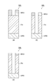
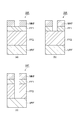
- FIG. 4A, FIG. 4B, FIG. 4C, and FIG. FIG. 4A is a partially enlarged cross-sectional view of an example substrate
- FIGS. 4B and 4C are diagrams of an example substrate in a state after execution of each of a plurality of steps of the method MT1. It is a partially expanded sectional view.
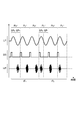
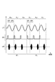
- FIG. 5 is an example timing chart related to the method MT1.
- the vertical axis indicates the first high-frequency power LF, the synchronization signal SS, and the second high-frequency power HF.
- Method MT1 includes step ST11 and step ST12.
- Step ST11 is executed in the first period P 1.
- First time length of the period P 1 of may be a time length m times the one cycle of the first high-frequency power LF. m is a natural number.
- Step ST12 is executed in the second period P 2.
- Second period P 2 is a period following the first period P 1.
- a second plasma process is performed. Duration of the second period P 2 may be a time length n times the one cycle of the first high-frequency power LF. n is a natural number.
- steps ST11 and ST12 a processing gas is supplied into the chamber 10.
- the gas supply unit GS is controlled by the control unit 80 to supply the processing gas.
- the exhaust unit 50 is controlled by the control unit 80 to set the pressure in the chamber 10 to the specified pressure.
- the pressure in the chamber 10 is set to, for example, a pressure in a range from several mTorr to 1000 mTorr.
- the first high-frequency power LF is continuously supplied to the lower electrode 18. That is, in the method MT1, the first high-frequency power LF is continuously fed to the first period P 1 and the second lower electrode 18 over a period P 2.
- the first high-frequency power supply unit 61 is controlled by the control unit 80 in order to supply the first high-frequency power LF to the lower electrode 18.
- the second high frequency power HF as pulsed RF power lower in the first within the first period P 1 of the inside part period SP 1 and the second inner portions period SP 2 in the second period P 2 It is supplied to the electrode 18 (or the upper electrode 30). That is, the second high frequency power HF is supplied as pulsed RF power at the step ST11 first inner portion period SP 1. The second high frequency power HF is supplied as pulsed RF power at the step ST12 second inner partial periods SP 2.
- the second high-frequency power supply unit 62 is controlled by the control unit 80 to supply the second high-frequency power HF.
- the first part period SP 1 is part of a period in each cycle P LF of the first high-frequency power LF.
- the second partial periods SP 2 is a part of the period in each cycle P LF of the first high-frequency power LF, a period different from the first sub-period.
- METHOD In MT1 the first part period SP 1, within each period P LF of the first high-frequency power LF, having a first high frequency power LF is negative potential output from the first RF power supply unit 61 It is included in a period (hereinafter, referred to as a “negative voltage output period”).
- the second partial periods SP 2 for a period of time in the first high frequency power LF output from the first high-frequency power supply 61 in each period P LF of the first high-frequency power LF has a positive voltage (Hereinafter, referred to as “positive voltage output period”).
- the second high-frequency power supply unit 62 can supply pulsed high-frequency power at appropriate timing in each cycle P LF specified by the synchronization signal SS in accordance with a command from the control unit 80. Therefore, in each of the plurality of first partial period SP 1, pulsed high-frequency power can be supplied at the same relative phase with respect to the period of the first high-frequency power LF. Further, in each of the plurality of second partial periods SP 2, pulsed high-frequency power can be supplied at the same relative phase with respect to the period of the first high-frequency power LF.
- the partial period (the first partial period SP 1 or the second partial period SP 2 ) set within the negative voltage output period is the first partial period SP 1 or the second partial period SP 2 within each cycle P LF of the first high-frequency power LF. It may include the point in time when one high frequency power LF has the minimum potential. Partial period set in the positive voltage output period (first part period SP 1 and the second partial periods SP 2), the first high-frequency power LF in each period P LF of the first high-frequency power LF It may include the time point with the highest potential.
- step ST11 plasma is formed from the processing gas in the chamber 10.
- the second high-frequency power HF is supplied as pulsed high-frequency power within the negative voltage output period. Therefore, in step ST11, Vpp (peak value of the voltage) of the substrate on the support 14 is increased, and the energy of ions traveling from the plasma toward the support 14 is relatively high.
- step ST12 the second high-frequency power HF is supplied as pulsed high-frequency power within the positive voltage output period. Therefore, in step ST12, the Vpp of the substrate on the support 14 is reduced, and the energy of ions traveling from the plasma to the support 14 is relatively low.
- the substrate WA to which the method MT1 can be applied has a base region URA and a film FA.
- the film FA is provided on the base region URA.
- the substrate WA may further have a mask MKA.
- the mask MKA is provided on the film FA.
- the mask MKA is patterned so as to partially expose the film FA.
- the base region URA is formed of silicon
- the film FA is formed of silicon oxide
- the mask MKA has a multilayer structure including a photoresist film and an anti-reflection film.
- the anti-reflection film of the mask MKA is provided on the film FA.
- the anti-reflection film of the mask MKA contains silicon.
- the photoresist film of the mask MKA is provided on the anti-reflection film of the mask MKA.
- substrate WA is for a first period P 1 and the second period P 2, is disposed in the chamber 10.
- the substrate WA is placed on a support 14 in the chamber 10.
- the processing gas used in step ST11 and step ST12 may include a fluorocarbon gas such as a C 4 F 8 gas.
- the processing gas used in step ST11 and step ST12 may further include an oxygen-containing gas such as O 2 gas and / or a rare gas such as argon gas.
- step ST11 the film FA is etched by ions from the plasma so as to expose the base region URA.
- Step ST11 is terminated when it is determined from the emission intensity obtained by the emission analyzer 54 that the etching amount of the film FA has decreased. For example, when it is determined that the emission intensity of CO acquired by the emission analyzer 54 is equal to or less than a predetermined value, the step ST11 is ended. Alternatively, the step ST11 ends after the elapse of the predetermined time.
- ions of high energy are supplied to the substrate WA, so that the film FA is etched at a high speed.
- step ST12 As shown in FIG. 4C, the film FA is over-etched.
- step ST12 ions of low energy are supplied to the substrate WA, so that the film FA can be over-etched while suppressing damage to the base region URA.
- FIG. 6 is a timing chart showing an example of the second high-frequency power as continuous high-frequency power.
- the second high-frequency power HF is supplied as one of a pulsed high-frequency power and a continuous high-frequency power in each cycle P LF in the first period P1, and the second high-frequency power is supplied in the second period.
- the power may be supplied as the other high-frequency power.
- the second high frequency power HF is in the first inner period P 1 is supplied as a pulse-like high-frequency power within a negative voltage output period, continuous in the second inner period P 2 It may be supplied as high frequency power.
- the energy of ions towards the support 14 is relatively high in the first inner period P 1, becomes relatively low in the second inner period P 2.
- the second high frequency power HF is in the first inner period P 1 is supplied as a continuous high-frequency power
- a second inner period P 2 as pulsed RF power to the positive voltage output period May be supplied.
- the energy of ions towards the support 14 is relatively high in the first inner period P 1, becomes relatively low in the second inner period P 2.
- FIG. 7 is a flowchart of a plasma processing method according to another exemplary embodiment.
- FIG. 8A is a partially enlarged cross-sectional view of an example substrate.
- FIGS. 8B to 8E are partially enlarged cross-sectional views of an example substrate in a state after execution of each of the plurality of steps of the method MT2 shown in FIG.
- the method MT2 illustrated in FIG. 7 includes a step ST21 and a step ST22.
- Step ST21 like step ST11 way MT1 is executed in the first period P 1.
- a first plasma process is performed.
- Step ST22 like step ST12 way MT1, is performed in the second period P 2.
- Second period P 2 is a period following the first period P 1.
- a second plasma process is performed.
- Method MT2 may further include step ST23 and step ST24.
- Step ST23 is performed in the third period.
- the third period is the period following the second period P 2.
- the time length of the third period may be p times the time length of one cycle of the first high-frequency power LF. p is a natural number.
- a third plasma process is performed in step ST23.
- Step ST24 is performed in the fourth period.
- the fourth period is a period following the third period.
- the time length of the fourth period may be q times the time length of one cycle of the first high-frequency power LF. q is a natural number.
- a fourth plasma process is performed.
- a processing gas is supplied into the chamber 10.
- the gas supply unit GS is controlled by the control unit 80 to supply the processing gas.
- the exhaust unit 50 is controlled by the control unit 80 to set the pressure in the chamber 10 to the specified pressure.
- the pressure in the chamber 10 is set to, for example, a pressure in a range from several mTorr to 1000 mTorr.
- the first high-frequency power LF is continuously supplied to the lower electrode 18. That is, in the method MT2, the first high-frequency power LF is continuously supplied to the lower electrode 18 for the first to fourth periods.
- the first high-frequency power supply unit 61 is controlled by the control unit 80 to supply the first high-frequency power LF to the lower electrode 18.
- the second high frequency power HF as pulsed RF power is supplied by a first inner portion period SP 1 in each of the first period P 1 and the third period. Further, the method MT2, the second high frequency power HF is a second inner partial periods SP 2 in each of the second period P 2 and the fourth period, is supplied to the lower electrode 18 (or the upper electrode 30) You. That is, the second high frequency power HF, in each of the steps ST21 and step ST23, supplied as pulsed RF power at a first inner portion period SP 1. The second high frequency power HF, in each of the steps ST22 and step ST24, supplied as a pulse-like high-frequency power in the second inner partial periods SP 2. In step ST21, step ST22, step ST23, and step ST24, the second high-frequency power supply unit 62 is controlled by the control unit 80 to supply the second high-frequency power HF.
- the first part period SP 1 is contained within the negative voltage output periods within each period P LF of the first high-frequency power LF.
- the second partial periods SP 2 is included in the positive voltage output periods within each period P LF of the first high-frequency power LF.
- steps ST21, ST22, ST23, and ST24 plasma is formed from the processing gas in the chamber 10.
- the second high-frequency power HF is supplied as pulsed high-frequency power within the negative voltage output period. Therefore, in steps ST21 and ST23, Vpp of the substrate on the support 14 is increased, and the energy of ions traveling from the plasma to the support 14 is relatively high.
- step ST22 and step ST24 the second high-frequency power HF is supplied as pulsed high-frequency power within the positive voltage output period. Therefore, in steps ST22 and ST24, the Vpp of the substrate on the support 14 is reduced, and the energy of ions traveling from the plasma toward the support 14 is relatively low.
- the substrate WB to which the method MT2 can be applied has a first film FB1 and a second film FB2.
- the first film FB1 is provided on the second film FB2.
- the substrate WB may further include a base region URB, a third film FB3, and a mask MKB.
- the third film FB3 is provided on the base region URB.
- the second film FB2 is provided on the third film FB3.
- the mask MKB is provided on the first film FB1.
- the mask MKB is patterned so as to partially expose the first film FB1.
- the base region URB is formed from silicon.
- the first film FB1 and the third film FB3 are formed from silicon oxide.
- the second film FB2 is formed from silicon nitride.
- the mask MKB is formed from a photoresist film.
- the substrate WB is placed in the chamber 10 for a first period to a fourth period.
- the substrate WB is placed on the support 14 in the chamber 10.
- Step ST21, the process gas used in the step ST22, step ST23, and step ST24 may include a fluorocarbon gas such as C 4 F 8 gas.
- the processing gas used in step ST21, step ST22, step ST23, and step ST24 may further include an oxygen-containing gas such as O 2 gas and / or a rare gas such as argon gas.
- step ST21 ions from the plasma are irradiated on the first film FB1, and the first film FB1 is etched so as to expose the second film FB2 by chemical ion etching. Is done.
- Step ST21 ends when it is determined from the emission intensity obtained by the emission analyzer 54 that the etching amount of the first film FB1 has decreased. For example, in step ST21, when it is determined that the emission intensity of CO obtained by the emission analyzer 54 is equal to or lower than a predetermined value, or when the emission intensity of CN obtained by the emission analyzer 54 is another predetermined value. If it is determined that this is the case, the process is terminated. Alternatively, the step ST21 ends after the elapse of the predetermined time.
- step ST22 ions from the plasma are irradiated on the second film FB2, and the second film FB2 is etched so as to expose the third film FB3 by chemical ion etching. Is done.
- Step ST22 ends when it is determined from the emission intensity obtained by the emission analyzer 54 that the etching amount of the second film FB2 has decreased. For example, in step ST22, when it is determined that the emission intensity of CN acquired by the emission analyzer 54 is equal to or less than a predetermined value, or when the emission intensity of CO acquired by the emission analyzer 54 is another predetermined value. If it is determined that this is the case, the process is terminated. Alternatively, the step ST22 ends after the elapse of the predetermined time.
- step ST23 ions from the plasma are irradiated on the third film FB3, and the third film FB3 is etched by chemical ion etching so as to expose the base region URB. .
- Step ST23 is terminated when it is determined from the emission intensity obtained by the emission analyzer 54 that the etching amount of the third film FB3 has decreased.
- the process ST23 is ended when it is determined that the emission intensity of CO acquired by the emission analyzer 54 is equal to or less than a predetermined value.
- the step ST23 is ended after the elapse of the predetermined time.
- the third film FB3 is over-etched.
- overetching of the third film FB3 can be performed while suppressing damage to the base region URB.
- this method MT2 it is possible to etch a multilayer film having a film that requires relatively high energy for the etching as the first film FB1, and a film that can be etched with relatively low energy as the second film FB2. It becomes. Further, between the second film FB2 and the base region URB, a multilayer film further having a film requiring relatively high energy as the third film FB3 can be etched.
- the second high-frequency power HF is supplied as one of a pulsed high-frequency power and a continuous high-frequency power in each cycle P LF in the first period P1, and in each period P LF in period P 2 of it may be supplied as the other high-frequency power. Further, in the method MT2, the second high-frequency power HF is supplied as one of the pulsed high-frequency power and the continuous high-frequency power in each cycle P LF in the third period, and the fourth high-frequency power is supplied in the fourth period. May be supplied as the other high-frequency power in each period P LF of .
- the second high-frequency power HF is supplied as pulsed high-frequency power within the negative voltage output period during the first and third periods, and is supplied as the second high-frequency power and the fourth period. During the period, it may be supplied as continuous high-frequency power. Also in this case, the energy of the ions traveling toward the support 14 is relatively high during the first period and the third period, and relatively low during the second period and the fourth period.
- the second high-frequency power HF is supplied as continuous high-frequency power during the first period and the third period, and during the second and fourth periods, the positive voltage output period It may be supplied as a pulsed high-frequency power inside. Also in this case, the energy of the ions traveling toward the support 14 is relatively high during the first period and the third period, and relatively low during the second period and the fourth period.
- FIG. 9 is a flowchart of a plasma processing method according to still another exemplary embodiment.
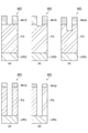
- FIG. 10A is a partially enlarged cross-sectional view of an example substrate.
- FIG. 10B is a partially enlarged cross-sectional view of one example of the substrate in a state after the execution of the step ST31 of the method MT3 shown in FIG.
- the method MT3 illustrated in FIG. 9 includes a step ST31 and a step ST32.
- Step ST31 like step ST11 way MT1 is executed in the first period P 1.
- a first plasma process is performed.
- Step ST32 like step ST12 way MT1, is performed in the second period P 2.
- Second period P 2 is the first or the first subsequent period to period P 1 after the period P 1.
- a second plasma process is performed.
- steps ST31 and ST32 a processing gas is supplied into the chamber 10.
- the gas supply unit GS is controlled by the control unit 80 to supply the processing gas.
- the control unit 80 controls the exhaust device 50 to set the pressure in the chamber 10 to the specified pressure.
- the first high-frequency power LF is continuously supplied to the lower electrode 18. That is, in the method MT3, the first high-frequency power LF is continuously fed to the first period P 1 and the second lower electrode 18 over a period P 2.
- the first high-frequency power supply unit 61 is controlled by the control unit 80 in order to supply the first high-frequency power LF to the lower electrode 18.
- the second high frequency power HF as pulsed RF power lower in the first within the first period P 1 of the inside part period SP 1 and the second inner portions period SP 2 in the second period P 2 It is supplied to the electrode 18 (or the upper electrode 30). That is, the second high frequency power HF is supplied as pulsed RF power at the step ST31 first inner portion period SP 1. The second high frequency power HF is supplied as pulsed RF power at the step ST32 second inner partial periods SP 2.
- the second high-frequency power supply unit 62 is controlled by the control unit 80 to supply the second high-frequency power HF.
- the first part period SP 1 is contained within the negative voltage output periods within each period P LF of the first high-frequency power LF.
- the second partial periods SP 2 is included in the positive voltage output periods within each period P LF of the first high-frequency power LF.
- step ST31 plasma is formed from the processing gas in the chamber 10.
- the second high-frequency power HF is supplied as pulsed high-frequency power within the negative voltage output period. Therefore, in step ST31, Vpp of the substrate on the support 14 is increased, and the energy of ions traveling from the plasma toward the support 14 is relatively high.
- step ST32 the second high frequency power HF is supplied as pulsed high frequency power within the positive voltage output period. Therefore, in step ST32, the Vpp of the substrate on the support 14 is reduced, and the energy of ions traveling from the plasma to the support 14 is relatively low. In step ST32, etching mainly using radicals is performed. Further, in step ST32, the energy of ions traveling toward the inner wall surface of the chamber 10, that is, the inner wall surface that defines the internal space 10s, becomes relatively high.
- the substrate WC to which the method MT3 can be applied has a base region URC and a film FC.
- the film FC is provided on the base region URC.
- the substrate WC may further have a mask MKC.
- the mask MKC is provided on the film FC.
- the mask MKC is patterned so as to partially expose the surface of the film FC.
- the base region URC is formed of TaN
- the film FC is a multilayer film including several magnetic layers
- the mask MKC is formed of silicon oxide.
- the multilayer film of the film FC is, for example, a multilayer film constituting an MRAM element portion, and includes an MTJ (Magnetic Tunnel Junction) structure.
- substrate WC in a first period P 1, is disposed in the chamber 10.
- the substrate WC is placed on the support 14 in the chamber 10.
- the processing gas used in step ST31 and step ST32 may be a mixed gas containing a rare gas such as a Cl 2 gas and an argon gas, or a mixed gas containing a CO gas and an NH 3 gas.
- step ST31 ions from plasma are irradiated to the film FC, and the film FC is etched by chemical ion etching and / or sputtering so as to expose the base region URC.
- Step ST31 is ended when it is determined from the emission intensity obtained by the emission analyzer 54 that the etching amount of the film FC has decreased.
- the step ST31 is ended after the elapse of the predetermined time.
- ions of high energy are supplied to the substrate WC, so that the film FC formed from the difficult-to-etch material can be etched.
- Method MT3 may further include step ST3a.
- Step ST3a is performed between step ST31 and step ST32.
- the substrate WC is carried out from the internal space 10s of the chamber 10. Therefore, step ST32 can be performed in a state where substrate WC is not arranged in chamber 10.
- Method MT3 may further include step ST3b.
- Step ST3b is performed between step ST3a and step ST32.
- step ST3b a dummy substrate is carried into the chamber 10. The dummy substrate is placed on the support 14. Therefore, step ST32 may be performed in a state where the dummy substrate is placed on support base 14.
- step ST31 the deposit adheres to the inner wall surface of the chamber 10.
- the deposit can be an etching by-product.
- step ST32 deposits attached to the inner wall surface of the chamber 10 are removed by chemical species such as ions and / or radicals from plasma.
- the energy of ions towards the support 14 is lowered, the energy of ions becomes higher toward the inner wall surface of the relatively chamber 10. As a result, deposits attached to the inner wall surface of the chamber 10 are efficiently removed.
- the second high-frequency power HF is supplied as one of the pulsed high-frequency power and the continuous high-frequency power in each cycle P LF in the first period P1, and in each period P LF in period P 2 of it may be supplied as the other high-frequency power.
- the second high frequency power HF is in the first inner period P 1 is supplied as a pulse-like high-frequency power within a negative voltage output period, continuous in the second inner period P 2 It may be supplied as high frequency power.
- the energy of the ions heading for the support 14 is relatively high during the first period and relatively low during the second period.
- the second high frequency power HF is in the first inner period P 1 is supplied as a continuous high-frequency power
- a second inner period P 2 pulsed RF power within the positive voltage output period It may be supplied as.
- the energy of the ions heading for the support 14 is relatively high during the first period and relatively low during the second period.
- FIG. 11 is a flowchart of a plasma processing method according to still another exemplary embodiment.
- FIG. 12A is a partially enlarged cross-sectional view of an example substrate.
- FIGS. 12B to 12D are partially enlarged cross-sectional views of an example substrate in a state after execution of each of the plurality of steps of the method MT4 shown in FIG.
- the method MT4 shown in FIG. 11 includes a step ST41 and a step ST42.
- Step ST41 like step ST11 way MT1 is executed in the first period P 1.
- the first period P 1 may be a period having a time length of the same and time length of a single period P LF.
- a first plasma process is performed in step ST42.
- Step ST42 like step ST12 way MT1, is performed in the second period P 2.
- Second period P 2 is a period following the first period P 1.
- Second period P 2 may be a period having a time length of the same and time length of a single period P LF.
- a second plasma process is performed.
- step ST41 a processing gas is supplied into the chamber 10.
- step ST42 the same processing gas as the processing gas used in step ST41 or another processing gas is supplied into the chamber 10.
- the gas supply unit GS is controlled by the control unit 80.
- step ST41 and step ST42 the exhaust unit 50 is controlled by the control unit 80 to set the pressure in the chamber 10 to the specified pressure.
- the pressure in the chamber 10 is set to, for example, a pressure in a range from several mmTorr to 1000 mTorr.
- the first high-frequency power LF is continuously supplied to the lower electrode 18. That is, in the method MT4, the first high-frequency power LF is continuously fed to the first period P 1 and the second lower electrode 18 over a period P 2.
- the first high-frequency power supply unit 61 is controlled by the control unit 80 to supply the first high-frequency power LF to the lower electrode 18.
- the second high frequency power HF as pulsed RF power lower in the first within the first period P 1 of the inside part period SP 1 and the second inner portions period SP 2 in the second period P 2 It is supplied to the electrode 18 (or the upper electrode 30). That is, the second high frequency power HF is supplied as pulsed RF power at the step ST41 first inner portion period SP 1. The second high frequency power HF is supplied as pulsed RF power at the step ST42 second inner partial periods SP 2.
- the second high-frequency power supply unit 62 is controlled by the control unit 80 to supply the second high-frequency power HF.
- first partial periods SP 1 is contained within the negative voltage output periods within each period P LF of the first high-frequency power LF.
- the second partial periods SP 2 is included in the positive voltage output periods within each period P LF of the first high-frequency power LF.
- step ST41 plasma is formed in the chamber 10.
- the second high frequency power HF is supplied as pulsed high frequency power within the negative voltage output period. Therefore, in step ST41, the Vpp of the substrate on the support 14 is increased, and the energy of ions traveling from the plasma to the support 14 is relatively high.
- step ST42 the second high-frequency power HF is supplied as pulsed high-frequency power within the positive voltage output period. Therefore, in step ST42, the Vpp of the substrate on the support 14 is reduced, and the energy of ions traveling from the plasma toward the support 14 is relatively low.
- substrate for a first period P 1 and the second period P 2 is disposed in the chamber 10.
- the substrate is placed on a support 14 in the chamber 10.
- the substrate WD to which the method MT4 can be applied has a base region URD and a film FD as shown in FIG.
- the film FD is provided on the base region URD.
- the substrate WD may further have a mask MKD.
- the mask MKD is provided on the film FD.
- the mask MKD is patterned so as to partially expose the surface of the film FD.
- the underlying region URD is formed of silicon oxide
- the film FD is an organic film or a silicon oxide film
- the mask MKD has a multilayer structure including a photoresist film and an anti-reflection film.
- the anti-reflection film of the mask MKD is provided on the film FD.
- the anti-reflection film of the mask MKD contains silicon.
- the photoresist film of the mask MKD is provided on the antireflection film of the mask MKD.
- the processing gas used in the step ST41 may include an oxygen-containing gas such as an O 2 gas.
- the processing gas used in the step ST41 may further include a rare gas such as an argon gas.
- the processing gas used in the process ST41 may include a fluorocarbon gas such as a C 4 F 8 gas.
- the processing gas used in the process ST41 includes a fluorocarbon gas such as a C 4 F 8 gas, an oxygen-containing gas such as an O 2 gas, and a rare gas such as an argon gas. It may be a mixed gas.
- the processing gas used in the step ST42 may include a fluorocarbon gas such as a C 4 F 8 gas, regardless of whether the film FD is an organic film or a silicon oxide film.
- the processing gas used in the step ST42 may further include an oxygen-containing gas such as an O 2 gas and a rare gas such as an argon gas.
- step ST41 the energy of the ions traveling toward the support 14 is relatively high. Therefore, in step ST41, the film FD is irradiated with ions from the plasma, and the film FD is etched by chemical ion etching. As shown in FIG. 12B, in step ST41, the film FD is etched so as to provide a side wall surface. In step ST42, the energy of the ions traveling toward the support 14 is relatively low. In step ST42, as shown in FIG. 12C, the chemical species from the plasma forms a film of the deposit DP on the surface of the substrate WD. The film of the deposit DP is formed from carbon and / or fluorocarbon species.
- step ST43 it is determined whether or not a stop condition is satisfied.
- the stop condition may be determined based on the emission intensity of the predetermined wavelength acquired by the emission analyzer 54, and may be determined based on the sequence including the steps ST41 and ST42 or the execution time length of the repetition of the sequence. The determination may be made based on this. If it is determined in step ST43 that the stop condition is not satisfied, the sequence including step ST41 and step ST42 is executed again.
- the etching in step ST41 has anisotropy. Therefore, in step ST41, as shown in FIG.
- step ST41 the deposit DP extending on the side wall surface of the substrate WD is left.
- step ST41 the deposit DP extending on another surface (horizontal plane) of the substrate W is removed, and the film FD is further etched. If it is determined in step ST43 that the stop condition is satisfied, the method MT4 ends.
- the steps ST41 and ST42 are alternately repeated. That is, in the method MT4, the formation of the deposit DP (step ST42) and the etching of the film FD (step ST41) are performed alternately. According to the method MT4, during the etching of the film FD, the side wall surface of the film FD is protected by the deposit DP.
- FIG. 13 is a flowchart of a plasma processing method according to still another exemplary embodiment.
- FIG. 14A is a partially enlarged cross-sectional view of an example substrate.
- 14 (b) to 14 (d) are partially enlarged cross-sectional views of an example substrate in a state after execution of each of the plurality of steps of the method MT5 shown in FIG.
- the method MT5 shown in FIG. 13 includes a step ST51 and a step ST52.
- Step ST51 like step ST51 way MT1 is executed in the first period P 1.
- the first period P 1 may be a period having a time length of the same and time length of a single period P LF.
- a first plasma process is performed in step ST51.
- Step ST52 like step ST12 way MT1, is performed in the second period P 2.
- Second period P 2 is a period following the first period P 1.
- Second period P 2 may be a period having a time length of the same and time length of a single period P LF.
- a second plasma process is performed.
- step ST51 a processing gas is supplied into the chamber 10.
- step ST52 the same processing gas as the processing gas used in step ST51 or another processing gas is supplied into the chamber 10.
- the gas supply unit GS is controlled by the control unit 80.
- the control unit 80 controls the exhaust device 50 to set the pressure in the chamber 10 to the specified pressure.
- the pressure in the chamber 10 is set to, for example, a pressure in a range from several mTorr to 1000 mTorr.
- Steps ST51 and ST52 the first high-frequency power LF is continuously supplied to the lower electrode 18. That is, in the method MT5, a first high-frequency power LF is continuously fed to the first period P 1 and the second lower electrode 18 over a period P 2.
- the first high-frequency power supply unit 61 is controlled by the control unit 80 in order to supply the first high-frequency power LF to the lower electrode 18.
- the second high frequency power HF as pulsed RF power lower in the first within the first period P 1 of the inside part period SP 1 and the second inner portions period SP 2 in the second period P 2 It is supplied to the electrode 18 (or the upper electrode 30). That is, the second high frequency power HF is supplied as pulsed RF power at the step ST51 first inner portion period SP 1. The second high frequency power HF is supplied as pulsed RF power at the step ST52 second inner partial periods SP 2.
- the second high-frequency power supply unit 62 is controlled by the control unit 80 to supply the second high-frequency power HF.
- a first partial periods SP 1 is contained within the negative voltage output periods within each period P LF of the first high-frequency power LF.
- second partial periods SP 2 is included in the positive voltage output periods within each period P LF of the first high-frequency power LF.
- step ST51 plasma is formed in the chamber 10.
- the second high frequency power HF is supplied as pulsed high frequency power within the negative voltage output period. Therefore, in step ST51, Vpp of the substrate on the support 14 is increased, and the energy of ions traveling from the plasma toward the support 14 is relatively high.
- step ST52 the second high-frequency power HF is supplied as pulsed high-frequency power within the positive voltage output period. Therefore, in step ST52, Vpp (peak value of the voltage) of the substrate on the support 14 is reduced, and the energy of ions traveling from the plasma to the support 14 is relatively low.
- substrate for a first period P 1 and the second period P 2, is disposed in the chamber 10.
- the substrate is placed on a support 14 in the chamber 10.
- the substrate WE to which the method MT5 can be applied has a base region URE and a film FE as shown in FIG.
- the film FE is provided on the base region URE.
- the substrate WE may further have a mask MKE.
- the mask MKE is provided on the film FE.
- the mask MKE is patterned so as to partially expose the surface of the film FE.
- the base region URE is formed from silicon oxide
- the film FE is formed from polycrystalline silicon
- the mask MKE is formed from silicon oxide.
- the processing gas used in step ST51 may include a halogen-containing gas such as a Cl 2 gas, an HBr gas, and an SF 6 gas.
- the processing gas used in step ST51 may further include an oxygen-containing gas such as an O 2 gas.
- the processing gas may include an oxygen-containing gas such as O 2 gas.
- the processing gas used in step ST52 may further include a rare gas such as an argon gas.
- step ST51 the energy of the ions traveling toward the support 14 is relatively high. Therefore, in step ST51, the film FE is irradiated with ions from the plasma, and the film FE is etched by chemical ion etching. As shown in FIG. 14B, in step ST51, the film FE is etched so as to provide a side wall surface. In step ST52, the energy of the ions traveling toward the support 14 is relatively low. In step ST52, as shown in FIG. 14C, the etching of the film FE is suppressed, and the region including the surface of the film FE is altered to form the altered region MR. For example, the altered region MR is formed by oxidation of silicon in a region including the surface of the film FE.
- step ST53 it is determined whether or not a stop condition is satisfied.
- the stop condition may be determined based on the emission intensity of a predetermined wavelength acquired by the emission analyzer 54, and may be determined based on the sequence including the steps ST51 and ST52 or the execution time length of the repetition of the sequence. The determination may be made based on this. If it is determined in step ST53 that the stop condition is not satisfied, the sequence including steps ST51 and ST52 is executed again. If it is determined in step ST53 that the stop condition is satisfied, the method MT5 ends.
- the steps ST51 and ST52 are alternately repeated. That is, according to the method MT5, the alteration processing of the film FE (step ST52) and the etching of the film FE (step ST51) are alternately performed. In the method MT5, since the side wall surface of the film FE is altered, the etching of the side wall surface in the step ST51 is suppressed as shown in FIG.
- FIG. 15 is a flowchart of a plasma processing method according to still another exemplary embodiment.
- FIG. 16A is a partially enlarged cross-sectional view of an example substrate.
- 16B and 16C are partially enlarged cross-sectional views of an example substrate in a state after execution of each of the plurality of steps of the method MT6 shown in FIG.
- FIG. 17 is an example timing chart related to the method MT6.
- the vertical axis indicates the first high-frequency power LF, the synchronization signal SS, and the second high-frequency power HF.
- the method MT6 shown in FIG. 15 includes a step ST61 and a step ST62.
- Step ST61 like step ST11 way MT1 is executed in the first period P 1.
- a first plasma process is performed.
- Step ST62 like step ST12 way MT1, is performed in the second period P 2.
- Second period P 2 is a period following the first period P 1.
- a second plasma process is performed.
- steps ST61 and ST62 a processing gas is supplied into the chamber 10.
- the gas supply unit GS is controlled by the control unit 80 to supply the processing gas.
- the exhaust unit 50 is controlled by the control unit 80 to set the pressure in the chamber 10 to the specified pressure.
- the pressure in the chamber 10 is set to, for example, a pressure in a range from several mTorr to 1000 mTorr.
- step ST61 and step ST62 the first high-frequency power LF is continuously supplied to the lower electrode 18. That is, in the method MT2, the first high-frequency power LF is continuously fed to the lower electrode 18 first period P 1 and for a second period P 2.
- the first high-frequency power supply section 61 is controlled by the control section 80 in order to supply the first high-frequency power LF to the lower electrode 18.
- the second high frequency power HF as pulsed RF power, the first part period SP within 1 in the first period P 1, and the second partial periods SP in the second period P 2 2 , it is supplied to the lower electrode 18 (or the upper electrode 30). That is, the second high frequency power HF is, in step ST61, supplied as pulsed RF power at a first inner portion period SP 1.
- the second high frequency power HF is, in step ST62, supplied as a pulse-like high-frequency power in the second inner partial periods SP 2.
- the second high-frequency power supply unit 62 is controlled by the control unit 80 to supply the second high-frequency power HF.
- first partial periods SP 1 are included within the positive voltage output periods within each period P LF of the first high-frequency power LF.
- the second partial periods SP 2 is included in the negative voltage output periods within each period P LF of the first high-frequency power LF.
- step ST61 plasma is formed from the processing gas in the chamber 10.
- step ST61 as shown in FIG. 17, the second high frequency power HF is supplied as pulsed high frequency power within the positive voltage output period. Therefore, in step ST61, the Vpp of the substrate on the support 14 is reduced, and the energy of ions traveling from the plasma to the support 14 is relatively low.
- step ST62 the second high-frequency power HF is supplied as pulsed high-frequency power within the negative voltage output period. Therefore, in step ST62, Vpp of the substrate on the support 14 is increased, and the energy of ions traveling from the plasma toward the support 14 is relatively high.
- the substrate WF to which the method MT6 can be applied has a first film FF1 and a second film FF2.
- the first film FF1 is provided on the second film FF2.
- the substrate WF may further have a base region URF and a mask MKF.
- the second film FF2 is provided on the base region URF.
- the mask MKF is provided on the first film FF1.
- the mask MKF is patterned so as to partially expose the first film FF1.
- the underlying region URF is formed from silicon.
- the first film FF1 is an antireflection film containing silicon.
- the second film FF2 is formed from silicon oxide.
- the mask MKF is formed from a photoresist film.
- substrate WF is the first period P 1 and for a second period of time P 2, is disposed in the chamber 10.
- the substrate WF is placed on the support 14 in the chamber 10.
- the processing gas used in step ST61 and step ST62 includes a fluorocarbon gas such as CF 4 gas.
- the processing gas used in step ST61 and step ST62 may further include a rare gas such as an argon gas.
- step ST61 the first film FF1 is irradiated with ions from the plasma so as to expose the second film FF2, and the first film FF1 is etched by chemical ion etching. Etched. Step ST61 is ended when it is determined from the emission intensity obtained by the emission analyzer 54 that the etching amount of the first film FF1 has decreased. Alternatively, the step ST61 ends after the elapse of the predetermined time.
- step ST62 ions from the plasma are irradiated on the second film FF2 so as to expose the base region URF, and the second film FF2 is etched by chemical ion etching.
- the step ST62 ends when it is determined from the emission intensity obtained by the emission analyzer 54 that the etching amount of the second film FB2 has decreased. For example, when it is determined that the emission intensity of CO acquired by the emission analyzer 54 is equal to or less than the predetermined value, the step ST62 is ended. Alternatively, the step ST62 ends after the elapse of the predetermined time.
- the second high-frequency power HF is supplied as one of the pulsed high-frequency power and the continuous high-frequency power in each cycle P LF in the first period P1, and in each period P LF in period P 2 of it may be supplied as the other high-frequency power.
- the second high frequency power HF is in the first inner period P 1 is supplied as a pulse-like high-frequency power within the positive voltage output period, continuous in the second inner period P 2 It may be supplied as high frequency power.
- the energy of ions towards the support table 14, the first period P 1 in a relatively low becomes the second relatively high in the period P 2 of.
- the second high frequency power HF is in the first inner period P 1 is supplied as a continuous high-frequency power, a second inner period P 2 pulsed RF power within a negative voltage output period It may be supplied as.
- FIG. 18 is a flowchart of a plasma processing method according to still another exemplary embodiment.
- FIG. 19 is a timing chart of an example related to the method MT7 shown in FIG.
- FIG. 20A is a partially enlarged cross-sectional view of an example substrate.
- FIGS. 20B to 20E are partially enlarged cross-sectional views of an example substrate after execution of each of the plurality of steps of the method MT7.
- the method MT7 shown in FIG. 18 includes a step ST71 and a step ST72.
- Step ST71 like step ST71 way MT1 is executed in the first period P 1.
- the first period P 1 is a period having a time length of the same and time length of a single period P LF.
- the first start of the period P 1 is coincident with the beginning of the corresponding period P LF.
- Step ST72 like step ST12 way MT1, is performed in the second period P 2.
- Second period P 2 is a period following the first period P 1.
- Second period P 2 is a period having a time length of the same and time length of a single period P LF. Beginning of the second period P 2 coincides with the beginning of the corresponding period P LF.
- a second plasma process is performed.
- the steps ST71 and ST72 are alternately repeated.
- Method MT7 may further include step ST73.
- step ST73 a third plasma process is performed.
- Step ST73 is executed in the third period P 3.
- Third period P 3 is followed in the period in which alternating repetition of steps ST71 and step ST72 is carried out for a period.
- a processing gas is supplied into the chamber 10.
- the gas supply unit GS is controlled by the control unit 80 to supply the processing gas into the chamber 10.
- the exhaust unit 50 is controlled by the control unit 80 to set the pressure in the chamber 10 to the specified pressure.
- the pressure in the chamber 10 is set to, for example, a pressure in a range from several mTorr to 1000 mTorr.
- step ST71, step ST72, and step ST73 the first high-frequency power LF is continuously supplied to the lower electrode 18. That is, in the method MT7, the first high-frequency power LF is continuously fed to the first period P 1 and the second lower electrode 18 over a period P 2. Further, the method MT7, the first high-frequency power LF, even in the third period P 3, are continuously fed. In step ST71, step ST72, and step ST73, the first high-frequency power supply unit 61 is controlled by the control unit 80 to supply the first high-frequency power LF to the lower electrode 18.
- the second high frequency power HF is supplied to the lower electrode 18 (or the upper electrode 30) as pulsed high frequency power. That is, in the method MT7, the second high frequency power HF is supplied to the lower electrode 18 (or the upper electrode 30) as pulsed RF power at a first inner period P 1. Specifically, the method MT7, as shown in FIG. 19, the second high frequency power HF includes a lower electrode 18 (or the upper electrode as a pulsed high-frequency power within the positive voltage output period of the first within the period P 1 30). In step ST72, the second high frequency power HF is not supplied. That is, the second high frequency power HF is not supplied in the second inner period P 2.
- step ST73 the second high frequency power HF is supplied to the lower electrode 18 (or the upper electrode 30) as pulsed RF power within a positive voltage output period in each cycle P LF.
- step ST71, step ST72, and step ST73 the second high-frequency power supply unit 62 is controlled by the control unit 80 to supply and stop the supply of the second high-frequency power HF.
- step ST71 plasma is generated from the processing gas in the chamber 10.
- the Vpp of the substrate on the support 14 in step ST72 is higher than the Vpp of the substrate on the support 14 in step ST71.
- step ST73 the second high frequency power HF is supplied as pulsed high frequency power within the positive voltage output period. Therefore, in step ST73, the Vpp of the substrate on the support 14 is reduced, and the energy of ions traveling from the plasma to the support 14 is relatively low.
- substrate In the method MT7, substrate, over a period and the third period P 3 consisting of the first period P 1 and the second repetition period P 2, is disposed in the chamber 10.
- the substrate is placed on a support 14 in the chamber 10.
- the substrate WG to which the method MT7 can be applied has a base region URG and a film FG as shown in FIG.
- the film FG is provided on the base region URG.
- the substrate WG may further have a mask MKG.
- the mask MKG is provided on the film FG.
- the mask MKG is patterned so as to partially expose the surface of the film FG.
- the base region URG is formed from silicon
- the film FG is formed from silicon oxide
- the mask MKG has a multilayer structure including a photoresist film and an antireflection film.
- the anti-reflection film of the mask MKG is provided on the film FG.
- the anti-reflection film of the mask MKG contains silicon.
- the photoresist film of the mask MKG is provided on the antireflection film of the mask MKG.
- Process gas used in the method MT7 may include a fluorocarbon gas such as C 4 F 8 gas.
- the processing gas used in the method MT7 may further include an oxygen-containing gas such as O 2 gas and a rare gas such as argon gas.
- VVpp of substrate WD in step ST71 is lower than Vpp of substrate WD in step ST72.
- step ST71 since the film FG is etched at a relatively low etching rate, the etching amount of the film FG is small as shown in FIG.
- step ST72 since the film FG is etched at a high etching rate, the etching amount of the film FG is large as shown in FIG.
- step ST7a it is determined whether or not the stop condition is satisfied.
- step ST7a it is determined that the stop condition is satisfied when the number of executions of the sequence including step ST71 and step ST72 reaches the predetermined number. If it is determined in step ST7a that the stop condition is not satisfied, the sequence including step ST71 and step ST72 is executed again. If it is determined in step ST7a that the stop condition is satisfied, the alternate repetition of step ST71 and step ST72 ends.
- the stop condition may be determined based on the emission intensity of a predetermined wavelength acquired by the emission analyzer 54, and may be determined based on the execution time length of the repetition of the sequence including the steps ST71 and ST72. May be done.
- step ST73 the film FG is over-etched as shown in FIG.
- step ST73 ions of low energy are supplied to the substrate WG, so that the film FG can be over-etched while suppressing damage to the base region URG.
- FIG. 21 is a flowchart of a plasma processing method according to still another exemplary embodiment.
- FIG. 22 is a timing chart of an example related to the method MT8 shown in FIG.
- Method MT8 shown in FIG. 21 includes step ST81 and step ST82. Step ST81 and step ST82 are alternately repeated. Step ST82 is the same step as step ST72. Method MT8 may further include step ST8a and step ST83. Step ST8a is the same step as step ST7a. In step ST8a, it is determined whether a stop condition is satisfied. In step ST8a, it is determined that the stop condition is satisfied when the number of executions of the sequence including step ST81 and step 82 has reached a predetermined number.
- the stop condition may be determined based on the emission intensity of a predetermined wavelength acquired by the emission analyzer 54, and may be determined based on the execution time length of the repetition of the sequence including the steps ST81 and ST82. May be done. If it is determined in step ST8a that the stop condition is not satisfied, the sequence including step ST81 and step ST82 is executed again. On the other hand, if it is determined in step ST8a that the stop condition is satisfied, step ST83 is executed. Step ST83 is the same step as step ST73.
- step ST81 the second high frequency power HF is as shown in FIG. 22, is supplied to the lower electrode 18 (or the upper electrode 30) as pulsed RF power within a negative voltage output period of the first within the period P 1 You.
- the processing in step ST81 is otherwise the same as the processing in step ST71.
- the energy of the ions colliding with the substrate in step ST81 is higher than the energy of the ions colliding with the substrate on the support 14 in step ST71. Therefore, the etching rate of the film in step ST81 of method MT8 is higher than the etching rate of the same film in step ST71. Further, the Vpp of the substrate on the support 14 in step ST82 is higher than the Vpp of the substrate on the support 14 in step ST81. Therefore, the method MT8, ions from the plasma generated in the first period P 1 collides with high energy substrates on the support base 14 in the second period P 2. This method MT8 can be performed using the same processing gas as the processing gas used in the method MT7 for etching and over-etching the film FG of the substrate WG.
- the energy of ions traveling toward the support 14 is adjusted in accordance with the mode of the second high-frequency power HF. Specifically, the energy of the ions traveling toward the support 14 differs depending on whether the second high-frequency power HF is supplied. The energy of ions toward the support 14 differs depending on whether the second high-frequency power HF is supplied as pulsed high-frequency power or continuous high-frequency power. The energy of the ions heading toward the support 14 changes according to the period during which the pulsed high-frequency power is supplied from the second high-frequency power HF in each cycle P LF of the first high-frequency power LF.
- the energy of ions traveling toward the support 14 is low when the second high-frequency power HF is supplied as pulsed high-frequency power during the positive voltage output period.
- the energy of the ions heading toward the support 14 is high when the second high frequency power HF is supplied as pulsed high frequency power during the negative voltage output period.
- the minimum time length during which the above-described mode is maintained may be set to the time length of one cycle of the first high-frequency power LF. Therefore, it is possible to change the energy of ions traveling toward the support 14 at high speed.
- the plasma processing methods according to various embodiments may be performed using an inductively coupled plasma processing apparatus.
- the second high frequency power is supplied to the antenna to form an inductive magnetic field in the chamber 10.
- Reference numeral 10 chamber, 14: support base, 18: lower electrode, LF: first high frequency power, HF: second high frequency power, P 1 : first period, P 2 : second period, P LF ... cycle .
Landscapes
- Physics & Mathematics (AREA)
- Engineering & Computer Science (AREA)
- Plasma & Fusion (AREA)
- Chemical & Material Sciences (AREA)
- Analytical Chemistry (AREA)
- Spectroscopy & Molecular Physics (AREA)
- Electromagnetism (AREA)
- Plasma Technology (AREA)
- Drying Of Semiconductors (AREA)
- Treatment Of Fiber Materials (AREA)
Priority Applications (6)
| Application Number | Priority Date | Filing Date | Title |
|---|---|---|---|
| CN202410297503.3A CN118197893A (zh) | 2018-06-22 | 2019-06-10 | Rf系统 |
| KR1020257021647A KR102962906B1 (ko) | 2018-06-22 | 2019-06-10 | 플라즈마 처리 방법 및 플라즈마 처리 장치 |
| KR1020207025526A KR20210019986A (ko) | 2018-06-22 | 2019-06-10 | 플라즈마 처리 방법 및 플라즈마 처리 장치 |
| US16/979,655 US11337297B2 (en) | 2018-06-22 | 2019-06-10 | Plasma processing method and plasma processing apparatus |
| CN201980017894.6A CN111837222B (zh) | 2018-06-22 | 2019-06-10 | 等离子体处理方法及等离子体处理装置 |
| US17/592,509 US11871503B2 (en) | 2018-06-22 | 2022-02-04 | Plasma processing method and plasma processing apparatus |
Applications Claiming Priority (2)
| Application Number | Priority Date | Filing Date | Title |
|---|---|---|---|
| JP2018119087A JP6846387B2 (ja) | 2018-06-22 | 2018-06-22 | プラズマ処理方法及びプラズマ処理装置 |
| JP2018-119087 | 2018-06-22 |
Related Child Applications (2)
| Application Number | Title | Priority Date | Filing Date |
|---|---|---|---|
| US16/979,655 A-371-Of-International US11337297B2 (en) | 2018-06-22 | 2019-06-10 | Plasma processing method and plasma processing apparatus |
| US17/592,509 Continuation US11871503B2 (en) | 2018-06-22 | 2022-02-04 | Plasma processing method and plasma processing apparatus |
Publications (1)
| Publication Number | Publication Date |
|---|---|
| WO2019244697A1 true WO2019244697A1 (ja) | 2019-12-26 |
Family
ID=68984039
Family Applications (1)
| Application Number | Title | Priority Date | Filing Date |
|---|---|---|---|
| PCT/JP2019/022952 Ceased WO2019244697A1 (ja) | 2018-06-22 | 2019-06-10 | プラズマ処理方法及びプラズマ処理装置 |
Country Status (6)
| Country | Link |
|---|---|
| US (2) | US11337297B2 (https=) |
| JP (1) | JP6846387B2 (https=) |
| KR (1) | KR20210019986A (https=) |
| CN (2) | CN118197893A (https=) |
| TW (1) | TWI815911B (https=) |
| WO (1) | WO2019244697A1 (https=) |
Cited By (16)
| Publication number | Priority date | Publication date | Assignee | Title |
|---|---|---|---|---|
| US11476145B2 (en) | 2018-11-20 | 2022-10-18 | Applied Materials, Inc. | Automatic ESC bias compensation when using pulsed DC bias |
| US11699572B2 (en) | 2019-01-22 | 2023-07-11 | Applied Materials, Inc. | Feedback loop for controlling a pulsed voltage waveform |
| US11791138B2 (en) | 2021-05-12 | 2023-10-17 | Applied Materials, Inc. | Automatic electrostatic chuck bias compensation during plasma processing |
| US11798790B2 (en) | 2020-11-16 | 2023-10-24 | Applied Materials, Inc. | Apparatus and methods for controlling ion energy distribution |
| US11848176B2 (en) | 2020-07-31 | 2023-12-19 | Applied Materials, Inc. | Plasma processing using pulsed-voltage and radio-frequency power |
| US11887813B2 (en) | 2021-06-23 | 2024-01-30 | Applied Materials, Inc. | Pulsed voltage source for plasma processing |
| US11901157B2 (en) | 2020-11-16 | 2024-02-13 | Applied Materials, Inc. | Apparatus and methods for controlling ion energy distribution |
| US11948780B2 (en) | 2021-05-12 | 2024-04-02 | Applied Materials, Inc. | Automatic electrostatic chuck bias compensation during plasma processing |
| US11967483B2 (en) | 2021-06-02 | 2024-04-23 | Applied Materials, Inc. | Plasma excitation with ion energy control |
| US11972924B2 (en) | 2022-06-08 | 2024-04-30 | Applied Materials, Inc. | Pulsed voltage source for plasma processing applications |
| US12106938B2 (en) | 2021-09-14 | 2024-10-01 | Applied Materials, Inc. | Distortion current mitigation in a radio frequency plasma processing chamber |
| US12198966B2 (en) | 2017-09-20 | 2025-01-14 | Applied Materials, Inc. | Substrate support with multiple embedded electrodes |
| US12261019B2 (en) | 2021-08-24 | 2025-03-25 | Applied Materials, Inc. | Voltage pulse time-domain multiplexing |
| US12272524B2 (en) | 2022-09-19 | 2025-04-08 | Applied Materials, Inc. | Wideband variable impedance load for high volume manufacturing qualification and on-site diagnostics |
| US12315732B2 (en) | 2022-06-10 | 2025-05-27 | Applied Materials, Inc. | Method and apparatus for etching a semiconductor substrate in a plasma etch chamber |
| US12586768B2 (en) | 2022-08-10 | 2026-03-24 | Applied Materials, Inc. | Pulsed voltage compensation for plasma processing applications |
Families Citing this family (15)
| Publication number | Priority date | Publication date | Assignee | Title |
|---|---|---|---|---|
| US10555412B2 (en) | 2018-05-10 | 2020-02-04 | Applied Materials, Inc. | Method of controlling ion energy distribution using a pulse generator with a current-return output stage |
| JP6846387B2 (ja) * | 2018-06-22 | 2021-03-24 | 東京エレクトロン株式会社 | プラズマ処理方法及びプラズマ処理装置 |
| JP7250663B2 (ja) * | 2018-12-19 | 2023-04-03 | 東京エレクトロン株式会社 | プラズマ処理装置及びインピーダンスの整合方法 |
| US11361947B2 (en) * | 2019-01-09 | 2022-06-14 | Tokyo Electron Limited | Apparatus for plasma processing and method of etching |
| US11508554B2 (en) | 2019-01-24 | 2022-11-22 | Applied Materials, Inc. | High voltage filter assembly |
| KR20220161452A (ko) | 2020-03-31 | 2022-12-06 | 램 리써치 코포레이션 | 염소 (chlorine) 를 사용한 고 종횡비 유전체 에칭 |
| US11495470B1 (en) | 2021-04-16 | 2022-11-08 | Applied Materials, Inc. | Method of enhancing etching selectivity using a pulsed plasma |
| US20220399186A1 (en) | 2021-06-09 | 2022-12-15 | Applied Materials, Inc. | Method and apparatus to reduce feature charging in plasma processing chamber |
| US12148595B2 (en) | 2021-06-09 | 2024-11-19 | Applied Materials, Inc. | Plasma uniformity control in pulsed DC plasma chamber |
| US12525441B2 (en) | 2021-06-09 | 2026-01-13 | Applied Materials, Inc. | Plasma chamber and chamber component cleaning methods |
| US11810760B2 (en) | 2021-06-16 | 2023-11-07 | Applied Materials, Inc. | Apparatus and method of ion current compensation |
| US11776788B2 (en) | 2021-06-28 | 2023-10-03 | Applied Materials, Inc. | Pulsed voltage boost for substrate processing |
| JP2024537515A (ja) * | 2021-11-03 | 2024-10-10 | ラム リサーチ コーポレーション | 高アスペクト比プラズマエッチングにおける金属含有表面の修正 |
| US11694876B2 (en) | 2021-12-08 | 2023-07-04 | Applied Materials, Inc. | Apparatus and method for delivering a plurality of waveform signals during plasma processing |
| US12111341B2 (en) | 2022-10-05 | 2024-10-08 | Applied Materials, Inc. | In-situ electric field detection method and apparatus |
Citations (4)
| Publication number | Priority date | Publication date | Assignee | Title |
|---|---|---|---|---|
| WO2017058341A1 (en) * | 2015-10-03 | 2017-04-06 | Applied Materials, Inc. | Rf power delivery with approximated saw tooth wave pulsing |
| WO2017126184A1 (ja) * | 2016-01-18 | 2017-07-27 | 株式会社 日立ハイテクノロジーズ | プラズマ処理方法およびプラズマ処理装置 |
| JP2018073904A (ja) * | 2016-10-26 | 2018-05-10 | 東京エレクトロン株式会社 | プラズマ処理装置のインピーダンス整合のための方法 |
| JP2018085389A (ja) * | 2016-11-21 | 2018-05-31 | 東芝メモリ株式会社 | ドライエッチング方法及び半導体装置の製造方法 |
Family Cites Families (56)
| Publication number | Priority date | Publication date | Assignee | Title |
|---|---|---|---|---|
| US5352324A (en) * | 1992-11-05 | 1994-10-04 | Hitachi, Ltd. | Etching method and etching apparatus therefor |
| JP3210469B2 (ja) | 1993-03-12 | 2001-09-17 | 株式会社日立製作所 | 半導体集積回路装置の製造方法 |
| US5614060A (en) * | 1995-03-23 | 1997-03-25 | Applied Materials, Inc. | Process and apparatus for etching metal in integrated circuit structure with high selectivity to photoresist and good metal etch residue removal |
| JP3612158B2 (ja) * | 1996-11-18 | 2005-01-19 | スピードファム株式会社 | プラズマエッチング方法及びその装置 |
| KR100521120B1 (ko) * | 1998-02-13 | 2005-10-12 | 가부시끼가이샤 히다치 세이사꾸쇼 | 반도체소자의 표면처리방법 및 장치 |
| KR100528685B1 (ko) * | 1998-03-12 | 2005-11-15 | 가부시끼가이샤 히다치 세이사꾸쇼 | 시료의 표면 가공방법 |
| US7212078B2 (en) * | 2003-02-25 | 2007-05-01 | Tokyo Electron Limited | Method and assembly for providing impedance matching network and network assembly |
| US9997338B2 (en) * | 2005-03-24 | 2018-06-12 | Oerlikon Surface Solutions Ag, Pfäffikon | Method for operating a pulsed arc source |
| JP5192209B2 (ja) * | 2006-10-06 | 2013-05-08 | 東京エレクトロン株式会社 | プラズマエッチング装置、プラズマエッチング方法およびコンピュータ読取可能な記憶媒体 |
| JP5491648B2 (ja) * | 2006-10-06 | 2014-05-14 | 東京エレクトロン株式会社 | プラズマエッチング装置およびプラズマエッチング方法 |
| JP5514413B2 (ja) * | 2007-08-17 | 2014-06-04 | 東京エレクトロン株式会社 | プラズマエッチング方法 |
| JP4607930B2 (ja) * | 2007-09-14 | 2011-01-05 | 株式会社東芝 | プラズマ処理装置およびプラズマ処理方法 |
| US20090139963A1 (en) * | 2007-11-30 | 2009-06-04 | Theodoros Panagopoulos | Multiple frequency pulsing of multiple coil source to control plasma ion density radial distribution |
| JP5319150B2 (ja) * | 2008-03-31 | 2013-10-16 | 東京エレクトロン株式会社 | プラズマ処理装置及びプラズマ処理方法及びコンピュータ読み取り可能な記憶媒体 |
| JP2010108997A (ja) * | 2008-10-28 | 2010-05-13 | Tokyo Electron Ltd | プラズマエッチング方法、プラズマエッチング装置及びコンピュータ記憶媒体 |
| JP5466480B2 (ja) * | 2009-02-20 | 2014-04-09 | 東京エレクトロン株式会社 | プラズマエッチング方法、プラズマエッチング装置および記憶媒体 |
| PL2236641T3 (pl) * | 2009-03-30 | 2012-05-31 | Oerlikon Trading Ag | Sposób wstępnej obróbki podłoży w procesie PVD |
| JP5662079B2 (ja) * | 2010-02-24 | 2015-01-28 | 東京エレクトロン株式会社 | エッチング処理方法 |
| JP5486383B2 (ja) * | 2010-04-13 | 2014-05-07 | 富士フイルム株式会社 | ドライエッチング方法及び装置 |
| US10157729B2 (en) * | 2012-02-22 | 2018-12-18 | Lam Research Corporation | Soft pulsing |
| US9295148B2 (en) * | 2012-12-14 | 2016-03-22 | Lam Research Corporation | Computation of statistics for statistical data decimation |
| US9043525B2 (en) * | 2012-12-14 | 2015-05-26 | Lam Research Corporation | Optimizing a rate of transfer of data between an RF generator and a host system within a plasma tool |
| WO2014164300A1 (en) * | 2013-03-13 | 2014-10-09 | Applied Materials, Inc | Pulsed pc plasma etching process and apparatus |
| CN103295870B (zh) * | 2013-06-05 | 2016-05-04 | 中微半导体设备(上海)有限公司 | 等离子体刻蚀设备及刻蚀方法 |
| JP6180824B2 (ja) * | 2013-07-02 | 2017-08-16 | 東京エレクトロン株式会社 | プラズマエッチング方法及びプラズマエッチング装置 |
| US9318304B2 (en) * | 2013-11-11 | 2016-04-19 | Applied Materials, Inc. | Frequency tuning for dual level radio frequency (RF) pulsing |
| JP6295119B2 (ja) * | 2014-03-25 | 2018-03-14 | 株式会社日立ハイテクノロジーズ | プラズマ処理装置 |
| JP6327970B2 (ja) * | 2014-06-19 | 2018-05-23 | 東京エレクトロン株式会社 | 絶縁膜をエッチングする方法 |
| KR102247560B1 (ko) * | 2014-07-14 | 2021-05-03 | 삼성전자 주식회사 | Rps에서의 플라즈마 생성방법, 및 그 플라즈마 생성방법을 포함한 반도체 소자 제조방법 |
| JP6512962B2 (ja) * | 2014-09-17 | 2019-05-15 | 東京エレクトロン株式会社 | プラズマ処理装置 |
| JPWO2016093269A1 (ja) * | 2014-12-12 | 2017-04-27 | 株式会社ダイヘン | 高周波電源 |
| US9779919B2 (en) * | 2015-01-09 | 2017-10-03 | Hitachi High-Technologies Corporation | Plasma processing apparatus and plasma processing method |
| JP6396822B2 (ja) * | 2015-02-16 | 2018-09-26 | 東京エレクトロン株式会社 | プラズマ処理装置のサセプタの電位を制御する方法 |
| JP6479562B2 (ja) * | 2015-05-07 | 2019-03-06 | 東京エレクトロン株式会社 | プラズマ処理装置の処理条件生成方法及びプラズマ処理装置 |
| US10622197B2 (en) * | 2015-07-21 | 2020-04-14 | Tokyo Electron Limited | Plasma processing apparatus and plasma processing method |
| US9947514B2 (en) * | 2015-09-01 | 2018-04-17 | Mks Instruments, Inc. | Plasma RF bias cancellation system |
| JP6670692B2 (ja) * | 2015-09-29 | 2020-03-25 | 株式会社日立ハイテク | プラズマ処理装置およびプラズマ処理方法 |
| US9577516B1 (en) * | 2016-02-18 | 2017-02-21 | Advanced Energy Industries, Inc. | Apparatus for controlled overshoot in a RF generator |
| US10229816B2 (en) * | 2016-05-24 | 2019-03-12 | Mks Instruments, Inc. | Solid-state impedance matching systems including a hybrid tuning network with a switchable coarse tuning network and a varactor fine tuning network |
| JP6820775B2 (ja) * | 2017-03-17 | 2021-01-27 | 株式会社日立ハイテク | エッチング方法及びプラズマ処理装置 |
| KR102475069B1 (ko) * | 2017-06-30 | 2022-12-06 | 삼성전자주식회사 | 반도체 제조 장치, 이의 동작 방법 |
| KR102435263B1 (ko) * | 2017-07-25 | 2022-08-23 | 삼성전자주식회사 | 플라즈마 처리 장치 및 방법, 및 이를 이용한 반도체 장치의 제조 방법 |
| JP7045152B2 (ja) * | 2017-08-18 | 2022-03-31 | 東京エレクトロン株式会社 | プラズマ処理方法及びプラズマ処理装置 |
| JP6937644B2 (ja) * | 2017-09-26 | 2021-09-22 | 東京エレクトロン株式会社 | プラズマ処理装置及びプラズマ処理方法 |
| KR20250153883A (ko) * | 2017-11-17 | 2025-10-27 | 에이이에스 글로벌 홀딩스 피티이 리미티드 | 플라즈마 프로세싱 시스템에서 변조 공급기들의 개선된 적용 |
| WO2019099870A1 (en) * | 2017-11-17 | 2019-05-23 | Advanced Energy Industries, Inc. | Synchronized pulsing of plasma processing source and substrate bias |
| JP2019186099A (ja) * | 2018-04-12 | 2019-10-24 | 東京エレクトロン株式会社 | プラズマ処理装置 |
| US10555412B2 (en) * | 2018-05-10 | 2020-02-04 | Applied Materials, Inc. | Method of controlling ion energy distribution using a pulse generator with a current-return output stage |
| JP6846387B2 (ja) * | 2018-06-22 | 2021-03-24 | 東京エレクトロン株式会社 | プラズマ処理方法及びプラズマ処理装置 |
| JP7175239B2 (ja) * | 2018-06-22 | 2022-11-18 | 東京エレクトロン株式会社 | 制御方法、プラズマ処理装置、プログラム及び記憶媒体 |
| JP7101096B2 (ja) * | 2018-10-12 | 2022-07-14 | 東京エレクトロン株式会社 | プラズマ処理方法及びプラズマ処理装置 |
| US11017985B2 (en) * | 2018-12-19 | 2021-05-25 | Tokyo Electron Limited | Plasma processing apparatus, impedance matching method, and plasma processing method |
| CN116844934A (zh) * | 2019-02-05 | 2023-10-03 | 东京毅力科创株式会社 | 等离子体处理装置 |
| JP7122268B2 (ja) * | 2019-02-05 | 2022-08-19 | 東京エレクトロン株式会社 | プラズマ処理装置 |
| US11177115B2 (en) * | 2019-06-03 | 2021-11-16 | Applied Materials, Inc. | Dual-level pulse tuning |
| US11232931B2 (en) * | 2019-10-21 | 2022-01-25 | Mks Instruments, Inc. | Intermodulation distortion mitigation using electronic variable capacitor |
-
2018
- 2018-06-22 JP JP2018119087A patent/JP6846387B2/ja active Active
-
2019
- 2019-06-10 US US16/979,655 patent/US11337297B2/en active Active
- 2019-06-10 KR KR1020207025526A patent/KR20210019986A/ko not_active Ceased
- 2019-06-10 WO PCT/JP2019/022952 patent/WO2019244697A1/ja not_active Ceased
- 2019-06-10 CN CN202410297503.3A patent/CN118197893A/zh active Pending
- 2019-06-10 CN CN201980017894.6A patent/CN111837222B/zh active Active
- 2019-06-18 TW TW108120966A patent/TWI815911B/zh active
-
2022
- 2022-02-04 US US17/592,509 patent/US11871503B2/en active Active
Patent Citations (4)
| Publication number | Priority date | Publication date | Assignee | Title |
|---|---|---|---|---|
| WO2017058341A1 (en) * | 2015-10-03 | 2017-04-06 | Applied Materials, Inc. | Rf power delivery with approximated saw tooth wave pulsing |
| WO2017126184A1 (ja) * | 2016-01-18 | 2017-07-27 | 株式会社 日立ハイテクノロジーズ | プラズマ処理方法およびプラズマ処理装置 |
| JP2018073904A (ja) * | 2016-10-26 | 2018-05-10 | 東京エレクトロン株式会社 | プラズマ処理装置のインピーダンス整合のための方法 |
| JP2018085389A (ja) * | 2016-11-21 | 2018-05-31 | 東芝メモリ株式会社 | ドライエッチング方法及び半導体装置の製造方法 |
Cited By (22)
| Publication number | Priority date | Publication date | Assignee | Title |
|---|---|---|---|---|
| US12198966B2 (en) | 2017-09-20 | 2025-01-14 | Applied Materials, Inc. | Substrate support with multiple embedded electrodes |
| US11476145B2 (en) | 2018-11-20 | 2022-10-18 | Applied Materials, Inc. | Automatic ESC bias compensation when using pulsed DC bias |
| US12057292B2 (en) | 2019-01-22 | 2024-08-06 | Applied Materials, Inc. | Feedback loop for controlling a pulsed voltage waveform |
| US11699572B2 (en) | 2019-01-22 | 2023-07-11 | Applied Materials, Inc. | Feedback loop for controlling a pulsed voltage waveform |
| US12237148B2 (en) | 2020-07-31 | 2025-02-25 | Applied Materials, Inc. | Plasma processing assembly using pulsed-voltage and radio-frequency power |
| US11848176B2 (en) | 2020-07-31 | 2023-12-19 | Applied Materials, Inc. | Plasma processing using pulsed-voltage and radio-frequency power |
| US11901157B2 (en) | 2020-11-16 | 2024-02-13 | Applied Materials, Inc. | Apparatus and methods for controlling ion energy distribution |
| US12183557B2 (en) | 2020-11-16 | 2024-12-31 | Applied Materials, Inc. | Apparatus and methods for controlling ion energy distribution |
| US11798790B2 (en) | 2020-11-16 | 2023-10-24 | Applied Materials, Inc. | Apparatus and methods for controlling ion energy distribution |
| US11948780B2 (en) | 2021-05-12 | 2024-04-02 | Applied Materials, Inc. | Automatic electrostatic chuck bias compensation during plasma processing |
| US11791138B2 (en) | 2021-05-12 | 2023-10-17 | Applied Materials, Inc. | Automatic electrostatic chuck bias compensation during plasma processing |
| US12347647B2 (en) | 2021-06-02 | 2025-07-01 | Applied Materials, Inc. | Plasma excitation with ion energy control |
| US11967483B2 (en) | 2021-06-02 | 2024-04-23 | Applied Materials, Inc. | Plasma excitation with ion energy control |
| US11887813B2 (en) | 2021-06-23 | 2024-01-30 | Applied Materials, Inc. | Pulsed voltage source for plasma processing |
| US12125673B2 (en) | 2021-06-23 | 2024-10-22 | Applied Materials, Inc. | Pulsed voltage source for plasma processing applications |
| US12261019B2 (en) | 2021-08-24 | 2025-03-25 | Applied Materials, Inc. | Voltage pulse time-domain multiplexing |
| US12106938B2 (en) | 2021-09-14 | 2024-10-01 | Applied Materials, Inc. | Distortion current mitigation in a radio frequency plasma processing chamber |
| US11972924B2 (en) | 2022-06-08 | 2024-04-30 | Applied Materials, Inc. | Pulsed voltage source for plasma processing applications |
| US12368020B2 (en) | 2022-06-08 | 2025-07-22 | Applied Materials, Inc. | Pulsed voltage source for plasma processing applications |
| US12315732B2 (en) | 2022-06-10 | 2025-05-27 | Applied Materials, Inc. | Method and apparatus for etching a semiconductor substrate in a plasma etch chamber |
| US12586768B2 (en) | 2022-08-10 | 2026-03-24 | Applied Materials, Inc. | Pulsed voltage compensation for plasma processing applications |
| US12272524B2 (en) | 2022-09-19 | 2025-04-08 | Applied Materials, Inc. | Wideband variable impedance load for high volume manufacturing qualification and on-site diagnostics |
Also Published As
| Publication number | Publication date |
|---|---|
| US11337297B2 (en) | 2022-05-17 |
| CN111837222B (zh) | 2024-04-09 |
| KR20250106324A (ko) | 2025-07-09 |
| KR20210019986A (ko) | 2021-02-23 |
| JP6846387B2 (ja) | 2021-03-24 |
| US20210051792A1 (en) | 2021-02-18 |
| CN111837222A (zh) | 2020-10-27 |
| CN118197893A (zh) | 2024-06-14 |
| US11871503B2 (en) | 2024-01-09 |
| TW202002722A (zh) | 2020-01-01 |
| US20220159820A1 (en) | 2022-05-19 |
| JP2019220650A (ja) | 2019-12-26 |
| TWI815911B (zh) | 2023-09-21 |
Similar Documents
| Publication | Publication Date | Title |
|---|---|---|
| JP6846387B2 (ja) | プラズマ処理方法及びプラズマ処理装置 | |
| JP7374362B2 (ja) | プラズマ処理方法及びプラズマ処理装置 | |
| JP7250663B2 (ja) | プラズマ処理装置及びインピーダンスの整合方法 | |
| EP2916344A1 (en) | Method of cleaning plasma processing apparatus | |
| JP7110034B2 (ja) | エッチングする方法及びプラズマ処理装置 | |
| JP2016105461A (ja) | 銅バリア膜をエッチングするための新規方法 | |
| US20140179106A1 (en) | In-situ metal residue clean | |
| US12230479B2 (en) | Processing chamber with multiple plasma units | |
| JP7101096B2 (ja) | プラズマ処理方法及びプラズマ処理装置 | |
| US11017985B2 (en) | Plasma processing apparatus, impedance matching method, and plasma processing method | |
| US20150311040A1 (en) | Plasma processing apparatus | |
| KR102840368B1 (ko) | 에칭 방법 및 기판 처리 장치 | |
| CN109755125A (zh) | 蚀刻方法 | |
| KR20210117944A (ko) | 에칭 방법 및 플라즈마 처리 장치 | |
| TW202018806A (zh) | 蝕刻方法及基板處理裝置 | |
| CN107785253A (zh) | 利用侧边溅射的线边缘粗糙表面改进 |
Legal Events
| Date | Code | Title | Description |
|---|---|---|---|
| 121 | Ep: the epo has been informed by wipo that ep was designated in this application |
Ref document number: 19822638 Country of ref document: EP Kind code of ref document: A1 |
|
| ENP | Entry into the national phase |
Ref document number: 20207025526 Country of ref document: KR Kind code of ref document: A |
|
| NENP | Non-entry into the national phase |
Ref country code: DE |
|
| 122 | Ep: pct application non-entry in european phase |
Ref document number: 19822638 Country of ref document: EP Kind code of ref document: A1 |
|
| WWR | Wipo information: refused in national office |
Ref document number: 1020207025526 Country of ref document: KR |
|
| WWP | Wipo information: published in national office |
Ref document number: 1020257021647 Country of ref document: KR |