WO2019244697A1 - Plasma processing method and plasma processing device - Google Patents
Plasma processing method and plasma processing device Download PDFInfo
- Publication number
- WO2019244697A1 WO2019244697A1 PCT/JP2019/022952 JP2019022952W WO2019244697A1 WO 2019244697 A1 WO2019244697 A1 WO 2019244697A1 JP 2019022952 W JP2019022952 W JP 2019022952W WO 2019244697 A1 WO2019244697 A1 WO 2019244697A1
- Authority
- WO
- WIPO (PCT)
- Prior art keywords
- frequency power
- period
- film
- supplied
- plasma processing
- Prior art date
Links
Images


Classifications
-
- H—ELECTRICITY
- H01—ELECTRIC ELEMENTS
- H01J—ELECTRIC DISCHARGE TUBES OR DISCHARGE LAMPS
- H01J37/00—Discharge tubes with provision for introducing objects or material to be exposed to the discharge, e.g. for the purpose of examination or processing thereof
- H01J37/32—Gas-filled discharge tubes
- H01J37/32009—Arrangements for generation of plasma specially adapted for examination or treatment of objects, e.g. plasma sources
- H01J37/32082—Radio frequency generated discharge
- H01J37/32137—Radio frequency generated discharge controlling of the discharge by modulation of energy
- H01J37/32155—Frequency modulation
- H01J37/32165—Plural frequencies
-
- H—ELECTRICITY
- H01—ELECTRIC ELEMENTS
- H01J—ELECTRIC DISCHARGE TUBES OR DISCHARGE LAMPS
- H01J37/00—Discharge tubes with provision for introducing objects or material to be exposed to the discharge, e.g. for the purpose of examination or processing thereof
- H01J37/32—Gas-filled discharge tubes
- H01J37/32009—Arrangements for generation of plasma specially adapted for examination or treatment of objects, e.g. plasma sources
- H01J37/32082—Radio frequency generated discharge
- H01J37/32174—Circuits specially adapted for controlling the RF discharge
-
- H—ELECTRICITY
- H05—ELECTRIC TECHNIQUES NOT OTHERWISE PROVIDED FOR
- H05H—PLASMA TECHNIQUE; PRODUCTION OF ACCELERATED ELECTRICALLY-CHARGED PARTICLES OR OF NEUTRONS; PRODUCTION OR ACCELERATION OF NEUTRAL MOLECULAR OR ATOMIC BEAMS
- H05H1/00—Generating plasma; Handling plasma
- H05H1/24—Generating plasma
- H05H1/46—Generating plasma using applied electromagnetic fields, e.g. high frequency or microwave energy
-
- H—ELECTRICITY
- H01—ELECTRIC ELEMENTS
- H01J—ELECTRIC DISCHARGE TUBES OR DISCHARGE LAMPS
- H01J37/00—Discharge tubes with provision for introducing objects or material to be exposed to the discharge, e.g. for the purpose of examination or processing thereof
- H01J37/32—Gas-filled discharge tubes
- H01J37/32009—Arrangements for generation of plasma specially adapted for examination or treatment of objects, e.g. plasma sources
- H01J37/32082—Radio frequency generated discharge
- H01J37/32137—Radio frequency generated discharge controlling of the discharge by modulation of energy
- H01J37/32146—Amplitude modulation, includes pulsing
-
- H—ELECTRICITY
- H01—ELECTRIC ELEMENTS
- H01J—ELECTRIC DISCHARGE TUBES OR DISCHARGE LAMPS
- H01J37/00—Discharge tubes with provision for introducing objects or material to be exposed to the discharge, e.g. for the purpose of examination or processing thereof
- H01J37/32—Gas-filled discharge tubes
- H01J37/32009—Arrangements for generation of plasma specially adapted for examination or treatment of objects, e.g. plasma sources
- H01J37/32082—Radio frequency generated discharge
- H01J37/32174—Circuits specially adapted for controlling the RF discharge
- H01J37/32183—Matching circuits
-
- H—ELECTRICITY
- H01—ELECTRIC ELEMENTS
- H01J—ELECTRIC DISCHARGE TUBES OR DISCHARGE LAMPS
- H01J37/00—Discharge tubes with provision for introducing objects or material to be exposed to the discharge, e.g. for the purpose of examination or processing thereof
- H01J37/32—Gas-filled discharge tubes
- H01J37/32431—Constructional details of the reactor
- H01J37/32532—Electrodes
- H01J37/32577—Electrical connecting means
-
- H—ELECTRICITY
- H01—ELECTRIC ELEMENTS
- H01J—ELECTRIC DISCHARGE TUBES OR DISCHARGE LAMPS
- H01J37/00—Discharge tubes with provision for introducing objects or material to be exposed to the discharge, e.g. for the purpose of examination or processing thereof
- H01J37/32—Gas-filled discharge tubes
- H01J37/32431—Constructional details of the reactor
- H01J37/32697—Electrostatic control
- H01J37/32706—Polarising the substrate
-
- H—ELECTRICITY
- H01—ELECTRIC ELEMENTS
- H01L—SEMICONDUCTOR DEVICES NOT COVERED BY CLASS H10
- H01L21/00—Processes or apparatus adapted for the manufacture or treatment of semiconductor or solid state devices or of parts thereof
- H01L21/02—Manufacture or treatment of semiconductor devices or of parts thereof
- H01L21/04—Manufacture or treatment of semiconductor devices or of parts thereof the devices having at least one potential-jump barrier or surface barrier, e.g. PN junction, depletion layer or carrier concentration layer
- H01L21/18—Manufacture or treatment of semiconductor devices or of parts thereof the devices having at least one potential-jump barrier or surface barrier, e.g. PN junction, depletion layer or carrier concentration layer the devices having semiconductor bodies comprising elements of Group IV of the Periodic System or AIIIBV compounds with or without impurities, e.g. doping materials
- H01L21/30—Treatment of semiconductor bodies using processes or apparatus not provided for in groups H01L21/20 - H01L21/26
- H01L21/302—Treatment of semiconductor bodies using processes or apparatus not provided for in groups H01L21/20 - H01L21/26 to change their surface-physical characteristics or shape, e.g. etching, polishing, cutting
- H01L21/306—Chemical or electrical treatment, e.g. electrolytic etching
- H01L21/3065—Plasma etching; Reactive-ion etching
-
- H—ELECTRICITY
- H01—ELECTRIC ELEMENTS
- H01L—SEMICONDUCTOR DEVICES NOT COVERED BY CLASS H10
- H01L21/00—Processes or apparatus adapted for the manufacture or treatment of semiconductor or solid state devices or of parts thereof
- H01L21/02—Manufacture or treatment of semiconductor devices or of parts thereof
- H01L21/04—Manufacture or treatment of semiconductor devices or of parts thereof the devices having at least one potential-jump barrier or surface barrier, e.g. PN junction, depletion layer or carrier concentration layer
- H01L21/18—Manufacture or treatment of semiconductor devices or of parts thereof the devices having at least one potential-jump barrier or surface barrier, e.g. PN junction, depletion layer or carrier concentration layer the devices having semiconductor bodies comprising elements of Group IV of the Periodic System or AIIIBV compounds with or without impurities, e.g. doping materials
- H01L21/30—Treatment of semiconductor bodies using processes or apparatus not provided for in groups H01L21/20 - H01L21/26
- H01L21/31—Treatment of semiconductor bodies using processes or apparatus not provided for in groups H01L21/20 - H01L21/26 to form insulating layers thereon, e.g. for masking or by using photolithographic techniques; After treatment of these layers; Selection of materials for these layers
- H01L21/3105—After-treatment
- H01L21/311—Etching the insulating layers by chemical or physical means
- H01L21/31105—Etching inorganic layers
- H01L21/31111—Etching inorganic layers by chemical means
- H01L21/31116—Etching inorganic layers by chemical means by dry-etching
-
- H—ELECTRICITY
- H01—ELECTRIC ELEMENTS
- H01L—SEMICONDUCTOR DEVICES NOT COVERED BY CLASS H10
- H01L21/00—Processes or apparatus adapted for the manufacture or treatment of semiconductor or solid state devices or of parts thereof
- H01L21/02—Manufacture or treatment of semiconductor devices or of parts thereof
- H01L21/04—Manufacture or treatment of semiconductor devices or of parts thereof the devices having at least one potential-jump barrier or surface barrier, e.g. PN junction, depletion layer or carrier concentration layer
- H01L21/18—Manufacture or treatment of semiconductor devices or of parts thereof the devices having at least one potential-jump barrier or surface barrier, e.g. PN junction, depletion layer or carrier concentration layer the devices having semiconductor bodies comprising elements of Group IV of the Periodic System or AIIIBV compounds with or without impurities, e.g. doping materials
- H01L21/30—Treatment of semiconductor bodies using processes or apparatus not provided for in groups H01L21/20 - H01L21/26
- H01L21/31—Treatment of semiconductor bodies using processes or apparatus not provided for in groups H01L21/20 - H01L21/26 to form insulating layers thereon, e.g. for masking or by using photolithographic techniques; After treatment of these layers; Selection of materials for these layers
- H01L21/32—Treatment of semiconductor bodies using processes or apparatus not provided for in groups H01L21/20 - H01L21/26 to form insulating layers thereon, e.g. for masking or by using photolithographic techniques; After treatment of these layers; Selection of materials for these layers using masks
-
- H—ELECTRICITY
- H01—ELECTRIC ELEMENTS
- H01L—SEMICONDUCTOR DEVICES NOT COVERED BY CLASS H10
- H01L21/00—Processes or apparatus adapted for the manufacture or treatment of semiconductor or solid state devices or of parts thereof
- H01L21/02—Manufacture or treatment of semiconductor devices or of parts thereof
- H01L21/04—Manufacture or treatment of semiconductor devices or of parts thereof the devices having at least one potential-jump barrier or surface barrier, e.g. PN junction, depletion layer or carrier concentration layer
- H01L21/18—Manufacture or treatment of semiconductor devices or of parts thereof the devices having at least one potential-jump barrier or surface barrier, e.g. PN junction, depletion layer or carrier concentration layer the devices having semiconductor bodies comprising elements of Group IV of the Periodic System or AIIIBV compounds with or without impurities, e.g. doping materials
- H01L21/30—Treatment of semiconductor bodies using processes or apparatus not provided for in groups H01L21/20 - H01L21/26
- H01L21/31—Treatment of semiconductor bodies using processes or apparatus not provided for in groups H01L21/20 - H01L21/26 to form insulating layers thereon, e.g. for masking or by using photolithographic techniques; After treatment of these layers; Selection of materials for these layers
- H01L21/3205—Deposition of non-insulating-, e.g. conductive- or resistive-, layers on insulating layers; After-treatment of these layers
- H01L21/321—After treatment
- H01L21/3213—Physical or chemical etching of the layers, e.g. to produce a patterned layer from a pre-deposited extensive layer
- H01L21/32133—Physical or chemical etching of the layers, e.g. to produce a patterned layer from a pre-deposited extensive layer by chemical means only
- H01L21/32135—Physical or chemical etching of the layers, e.g. to produce a patterned layer from a pre-deposited extensive layer by chemical means only by vapour etching only
- H01L21/32136—Physical or chemical etching of the layers, e.g. to produce a patterned layer from a pre-deposited extensive layer by chemical means only by vapour etching only using plasmas
-
- H—ELECTRICITY
- H01—ELECTRIC ELEMENTS
- H01J—ELECTRIC DISCHARGE TUBES OR DISCHARGE LAMPS
- H01J2237/00—Discharge tubes exposing object to beam, e.g. for analysis treatment, etching, imaging
- H01J2237/32—Processing objects by plasma generation
- H01J2237/33—Processing objects by plasma generation characterised by the type of processing
- H01J2237/334—Etching
- H01J2237/3341—Reactive etching
Definitions
- the exemplary embodiment of the present disclosure relates to a plasma processing method and a plasma processing apparatus.
- plasma processing is performed using a plasma processing apparatus.
- the plasma processing apparatus includes a chamber and a substrate support.
- the substrate support includes a lower electrode and is provided in the chamber.
- high-frequency power is supplied to excite a gas in a chamber, and plasma is generated from the gas.
- another high-frequency power can be supplied to the lower electrode.
- Another high frequency power has a lower frequency than the frequency of the high frequency power for plasma generation. That is, another high frequency power is a bias high frequency power.
- the bias radio frequency power is used to adjust the energy of ions that collide with a substrate provided on a substrate support. The energy of the ions impinging on the substrate will be higher if a bias RF power having a higher power level is supplied to the lower electrode. On the other hand, the energy of the ions colliding with the substrate will be lower if a bias RF power having a lower power level is supplied to the lower electrode.
- Patent Document 1 describes a plasma treatment for etching a silicon nitride film.
- the power level of the bias high-frequency power is set to a high level during the etching of the silicon nitride film.
- the power level of the bias high-frequency power becomes high. And alternately to a lower level.
- a plasma processing method includes performing a first plasma process in a chamber during a first time period, and performing a second plasma process in the chamber during a second time period after the first time period or subsequent to the first time period. Performing a process.
- the first high frequency power is continuously supplied to the lower electrode of the substrate support in the step of performing the first plasma processing and the step of performing the second plasma processing.
- the first high frequency power has a first frequency.
- the substrate support is provided in the chamber.
- the second high-frequency power is supplied as pulsed high-frequency power in a first partial period of the first period and in a second partial period of the second period.
- the second high frequency power is a high frequency power for plasma generation having a second frequency higher than the first frequency.
- the first partial period is a partial period in each cycle of the first high-frequency power.
- the second partial period is a partial period in each cycle of the first high-frequency power and is different from the first partial period.
- the second high-frequency power is supplied as one of a pulsed high-frequency power and a continuous high-frequency power in each cycle of the first high-frequency power in the first period, and Within each period of the first high-frequency power in the period, it is supplied as the other high-frequency power.
- the second high-frequency power is supplied as pulsed high-frequency power in each cycle of the first high-frequency power in the first period, and is not supplied in the second period.
- the plasma processing method it is possible to rapidly change the energy of ions traveling toward the substrate support.
- FIG. 3 is a flowchart of a plasma processing method according to one exemplary embodiment.
- FIG. 1 schematically illustrates a plasma processing apparatus according to one exemplary embodiment.
- FIG. 4 is a diagram schematically illustrating a plasma processing apparatus according to another exemplary embodiment.
- FIG. 4A is a partially enlarged cross-sectional view of an example substrate
- FIGS. 4B and 4C are diagrams of an example substrate in a state after execution of each of a plurality of steps of the method MT1. It is a partially expanded sectional view.
- 6 is an example timing chart related to the method MT1. It is a timing chart which shows an example of 2nd high frequency power as continuous high frequency power.
- 5 is a flowchart of a plasma processing method according to another exemplary embodiment.
- FIG. 1 schematically illustrates a plasma processing apparatus according to one exemplary embodiment.
- FIG. 4 is a diagram schematically illustrating a plasma processing apparatus according to another exemplary embodiment.
- FIG. 4A is a partially enlarged
- FIG. 8A is a partially enlarged cross-sectional view of an example of a substrate
- FIGS. 8B to 8E are examples of a state after execution of each of the plurality of steps of the method MT2.
- FIG. 4 is a partially enlarged cross-sectional view of a substrate.
- FIG. 9 is a flowchart of a plasma processing method according to still another exemplary embodiment.
- FIG. 10A is a partially enlarged cross-sectional view of one example of the substrate, and FIG. 10B is a partially enlarged view of one example of the substrate in a state after the step ST31 of the method MT3 shown in FIG. It is sectional drawing.
- FIG. 11 is a flowchart of a plasma processing method according to still another exemplary embodiment.
- FIG. 12A is a partially enlarged cross-sectional view of an example of a substrate
- FIGS. 12B to 12D show a plurality of steps of the method MT4 shown in FIG.
- FIG. 4 is a partially enlarged cross-sectional view of an example substrate in a state.
- 9 is a flowchart of a plasma processing method according to still another exemplary embodiment.
- FIG. 14A is a partially enlarged cross-sectional view of one example of a substrate, and FIGS. 14B to 14D are views after execution of each of a plurality of steps of the method MT5 shown in FIG.
- FIG. 4 is a partially enlarged cross-sectional view of an example substrate in a state.
- 9 is a flowchart of a plasma processing method according to still another exemplary embodiment.
- FIG. 14A is a partially enlarged cross-sectional view of one example of a substrate
- FIGS. 14B to 14D are views after execution of each of a plurality of steps of the method MT
- FIG. 16A is a partially enlarged cross-sectional view of an example of a substrate
- FIGS. 16B and 16C show a plurality of steps of the method MT6 shown in FIG.
- FIG. 4 is a partially enlarged cross-sectional view of an example substrate in a state.
- 9 is an example timing chart related to the method MT6.
- 9 is a flowchart of a plasma processing method according to still another exemplary embodiment.
- 19 is a timing chart of an example related to the method MT7 shown in FIG.
- FIG. 20A is a partially enlarged cross-sectional view of an example substrate
- FIGS. 20B to 20E are views of the example substrate after each of a plurality of steps of the method MT7. It is a partially expanded sectional view.
- 9 is a flowchart of a plasma processing method according to still another exemplary embodiment.
- 22 is a timing chart illustrating an example related to the method MT8 illustrated in FIG. 21.
- a plasma processing method includes performing a first plasma process in a chamber during a first time period, and performing a second plasma process in the chamber during a second time period after the first time period or subsequent to the first time period. Performing a process.
- the first high frequency power is continuously supplied to the lower electrode of the substrate support in the step of performing the first plasma processing and the step of performing the second plasma processing.
- the first high frequency power has a first frequency.
- the substrate support is provided in the chamber.
- the second high-frequency power is supplied as pulsed high-frequency power in a first partial period of the first period and in a second partial period of the second period.
- the second high frequency power is a high frequency power for plasma generation having a second frequency higher than the first frequency.
- the first partial period is a partial period in each cycle of the first high-frequency power.
- the second partial period is a partial period in each cycle of the first high-frequency power and is different from the first partial period.
- the second high-frequency power is supplied as one of a pulsed high-frequency power and a continuous high-frequency power in each cycle of the first high-frequency power in the first period, and Within each period of the first high-frequency power in the period, it is supplied as the other high-frequency power.
- the second high-frequency power is supplied as pulsed high-frequency power in each cycle of the first high-frequency power in the first period, and is not supplied in the second period.
- the energy of the ions traveling toward the substrate support is different depending on the mode of the second high-frequency power. Specifically, the energy of the ions heading for the substrate support differs depending on whether or not the second high-frequency power is supplied. The energy of the ions toward the substrate support depends on whether the second high frequency power is supplied as pulsed high frequency power or continuous high frequency power. The energy of the ions heading toward the substrate support changes in accordance with the period during which the pulsed high-frequency power is supplied in each cycle of the second high-frequency power and the first high-frequency power.
- the second high-frequency power is supplied as pulsed high-frequency power within a period in which the first high-frequency power output from the first high-frequency power supply has a positive potential. If it is low.
- the energy of the ions heading toward the substrate support is such that the second high-frequency power is supplied as pulsed high-frequency power during a period in which the first high-frequency power output from the first high-frequency power supply has a negative potential. If high.
- the minimum time length during which the above-described mode is maintained may be set to the time length of one cycle of the first high-frequency power. Therefore, it is possible to change the energy of the ions traveling toward the substrate support at high speed.
- the second high frequency power is within a first sub-period within the first period and within a second sub-period within the second period. Is supplied as pulsed high-frequency power.
- the first partial period is included in a period in which the first high-frequency power output from the first high-frequency power supply unit has a negative potential in each cycle of the first high-frequency power.
- the second partial period is included in a period in which the first high-frequency power output from the first high-frequency power supply unit has a positive voltage in each cycle of the first high-frequency power.
- the energy of the ions towards the substrate support is high during the first time period and low during the second time period.
- the second high-frequency power is output from the first high-frequency power supply within each period of the first high-frequency power in the first period. During the period in which the first high-frequency power has a negative potential, it is supplied as pulsed high-frequency power. The second high-frequency power is supplied as continuous high-frequency power in each cycle of the first high-frequency power in the second period.
- the energy of the ions towards the substrate support is high during a first time period and low during a second time period.
- the second high frequency power is provided as a continuous high frequency power within each period of the first high frequency power within a first time period.
- the second high-frequency power has a pulse shape during a period in which the first high-frequency power output from the first high-frequency power supply unit has a positive voltage in each cycle of the first high-frequency power in the second period. It is supplied as high frequency power.
- the energy of the ions towards the substrate support is high during the first time period and low during the second time period.
- a substrate is disposed in a chamber for a first period and a second period.
- the substrate has a base region and a film provided on the base region.
- the film is etched using the processing gas plasma so as to expose the underlying region.
- the film is further etched using the plasma of the processing gas.
- the energy of the ions is reduced during overetching of the film. Therefore, damage to the underlying region is suppressed.
- a substrate is disposed in a chamber for a first period and a second period.
- the substrate has a first film and a second film.
- the first film is provided on the second film.
- the first film is etched using the plasma of the processing gas.
- the second film is etched using the plasma of the processing gas.
- a substrate is placed in a chamber during a first time period.
- the film of the substrate is etched using the plasma of the processing gas.
- the substrate is not placed in the chamber.
- Deposits adhering to the inner wall surface of the chamber are removed using the processing gas plasma in the step of performing the second plasma processing.
- the energy of ions traveling toward the substrate support becomes low, and the energy of ions traveling toward the inner wall surface of the chamber becomes relatively high. As a result, deposits attached to the inner wall surface of the chamber are efficiently removed.
- a substrate is placed in a chamber for a first period and a second period.
- the film of the substrate is etched using the plasma of the process gas to provide a sidewall surface.
- a chemical species from the processing gas plasma or another processing gas from the plasma of the processing gas is deposited on the surface of the substrate whose film has been etched in the step of performing the first plasma processing.
- a deposit containing the species is formed.
- deposit formation and film etching are alternated. During the etching of the film, the sidewall surfaces of the film are protected by the deposit.
- a substrate is placed in a chamber over a first time period and a second time period.
- the film of the substrate is etched using the plasma of the process gas to provide a sidewall surface.
- the surface of the film etched in the step of performing the first plasma processing is altered using plasma of a processing gas or another processing gas.
- the step of performing the first plasma processing and the step of performing the second plasma processing are alternately repeated.
- alteration of the film and etching of the film are performed alternately. Since the side wall surface of the film is altered, the etching of the side wall surface is suppressed during the etching of the film.
- the second high frequency power is within a first sub-period within a first period and within a second sub-period within a second period. Is supplied as pulsed high-frequency power.
- the first partial period is included in a period in which the first high-frequency power output from the first high-frequency power supply unit has a positive voltage in each cycle of the first high-frequency power.
- the second partial period is included in a period in which the first high-frequency power output from the first high-frequency power supply unit has a negative potential in each cycle of the first high-frequency power.
- the energy of the ions toward the substrate support is low during the first time period and high during the second time period.
- the second high frequency power is output from the first high frequency power supply within each cycle of the first high frequency power within the first period.
- the first high-frequency power has a positive voltage
- it is supplied as pulsed high-frequency power.
- the second high-frequency power is supplied as continuous high-frequency power in each cycle of the first high-frequency power in the second period.
- the energy of the ions toward the substrate support is low during a first time period and high during a second time period.
- the second high frequency power is provided as a continuous high frequency power within each period of the first high frequency power within a first time period.
- the second high-frequency power has a pulse-like shape during a period in which the first high-frequency power output from the first high-frequency power supply unit has a negative potential in each cycle of the first high-frequency power in the second period. It is supplied as high frequency power.
- the energy of the ions toward the substrate support is low during a first time period and high during a second time period.
- the substrate is disposed in the chamber for a first period and a second period.
- the substrate has a first film and a second film, and the first film is provided over the second film.
- the first film is etched using the plasma of the processing gas.
- the second film is etched using the plasma of the processing gas.
- each of the first period and the second period has the same time length as one period of the first high-frequency power.
- the second high-frequency power is supplied as pulsed high-frequency power during a period in which the first high-frequency power output from the first high-frequency power supply unit has a negative potential within the first period.
- the second high frequency power is not supplied within the second period.
- the step of performing the first plasma processing and the step of performing the second plasma processing are alternately repeated so as to etch the film of the substrate disposed in the chamber. According to a fourteenth exemplary embodiment, ions generated during a first time period strike the substrate with high energy during a second time period.
- each of the first period and the second period has the same time length as one period of the first high-frequency power.
- the second high-frequency power is supplied as pulsed high-frequency power during a period in which the first high-frequency power output from the first high-frequency power supply unit has a positive voltage within the first period.
- the second high frequency power is not supplied within the second period.
- the step of performing the first plasma processing and the step of performing the second plasma processing are alternately repeated so as to etch the film of the substrate disposed in the chamber. According to a fifteenth exemplary embodiment, ions generated during a first time period strike the substrate with high energy during a second time period.
- a plasma processing apparatus in another exemplary embodiment, includes a chamber, a substrate support, a first high-frequency power supply, a second high-frequency power supply, and a controller.
- the substrate support includes a lower electrode and is provided in the chamber.
- the first high-frequency power supply unit is configured to supply a first high-frequency power having a first frequency to the lower electrode.
- the second high-frequency power supply is configured to supply a second high-frequency power having a second frequency higher than the first frequency to generate plasma.
- the control unit is configured to control the first high-frequency power supply unit and the second high-frequency power supply unit.
- the control unit is configured to control the first high-frequency power supply unit to continuously supply the first high-frequency power to the lower electrode in the first period and in a second period after the first period or in a second period following the first period. Control.
- the control unit supplies the second high-frequency power as pulsed high-frequency power in a first partial period of the first period, and supplies a second high-frequency power in a second partial period of the second period.
- the second high frequency power supply is controlled so as to supply the high frequency power as pulsed high frequency power.
- the first partial period is a partial period in each cycle of the first high-frequency power.
- the second partial period is a partial period within each cycle of the first high-frequency power, and is different from the first partial period.
- the control unit supplies the second high-frequency power as one of the pulsed high-frequency power and the continuous high-frequency power in each cycle of the first high-frequency power in the first period.
- the second high-frequency power supply unit is controlled.
- the control unit controls the second high-frequency power supply unit so as to supply the second high-frequency power as the other high-frequency power in each cycle of the first high-frequency power in the second period.
- the control unit supplies the second high-frequency power as pulsed high-frequency power in each cycle of the first high-frequency power in the first period, and supplies the second high-frequency power in the second period.
- the second high-frequency power supply unit is controlled so as not to be supplied.
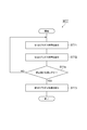
- FIG. 1 is a flowchart of a plasma processing method according to one exemplary embodiment.
- the plasma processing method shown in FIG. 1 (hereinafter, referred to as “method MT1”) is performed using a plasma processing apparatus.
- FIG. 2 is a diagram schematically illustrating a plasma processing apparatus according to one exemplary embodiment.
- the plasma processing apparatus shown in FIG. 2 can be used for performing the plasma processing method according to various embodiments of the present disclosure.
- the plasma processing apparatus 1A shown in FIG. 2 is a capacitively-coupled plasma processing apparatus.
- the plasma processing apparatus 1A includes a chamber 10.
- the chamber 10 provides an internal space 10s therein.
- the chamber 10 includes a chamber body 12.
- the chamber main body 12 has a substantially cylindrical shape.
- the internal space 10 s is provided inside the chamber main body 12.
- the chamber main body 12 is formed of, for example, aluminum.
- a film having corrosion resistance is provided on the inner wall surface of the chamber main body 12.
- the film having corrosion resistance may be a film formed from a ceramic such as aluminum oxide or yttrium oxide.
- a passage 12p is formed in the side wall of the chamber body 12.
- the substrate W passes through the passage 12p when transported between the internal space 10s and the outside of the chamber 10.
- the passage 12p can be opened and closed by a gate valve 12g.
- the gate valve 12g is provided along the side wall of the chamber main body 12.
- a support 13 is provided on the bottom of the chamber body 12.
- the support 13 is formed from an insulating material.
- the support part 13 has a substantially cylindrical shape.
- the support portion 13 extends upward from the bottom of the chamber body 12 in the internal space 10s.
- the support 13 supports a substrate support, that is, a support 14.
- the support 14 is provided in the internal space 10s.
- the support base 14 is configured to support the substrate W in the chamber 10, that is, in the internal space 10s.
- the support 14 has a lower electrode 18 and an electrostatic chuck 20.
- the support 14 may further include an electrode plate 16.
- the electrode plate 16 is formed of a conductor such as aluminum, for example, and has a substantially disk shape.
- the lower electrode 18 is provided on the electrode plate 16.
- the lower electrode 18 is formed of a conductor such as aluminum, and has a substantially disk shape.
- the lower electrode 18 is electrically connected to the electrode plate 16.
- the electrostatic chuck 20 is provided on the lower electrode 18.
- the substrate W is placed on the upper surface of the electrostatic chuck 20.
- the electrostatic chuck 20 has a main body and an electrode.
- the main body of the electrostatic chuck 20 has a substantially disk shape and is formed of a dielectric.
- the electrode of the electrostatic chuck 20 is a film-shaped electrode, and is provided in the main body of the electrostatic chuck 20.
- the electrode of the electrostatic chuck 20 is connected to a DC power supply 20p via a switch 20s. When a voltage from the DC power supply 20p is applied to the electrodes of the electrostatic chuck 20, an electrostatic attraction is generated between the electrostatic chuck 20 and the substrate W.
- the substrate W is attracted to the electrostatic chuck 20 by the generated electrostatic attraction, and is held by the electrostatic chuck 20.
- a focus ring FR is arranged on the periphery of the lower electrode 18 so as to surround the edge of the substrate W.
- the focus ring FR is provided to improve the in-plane uniformity of the plasma processing on the substrate W.
- the focus ring FR can be formed from, but not limited to, silicon, silicon carbide, or quartz.
- a flow path 18f is provided inside the lower electrode 18.
- a heat exchange medium for example, a refrigerant
- the heat exchange medium supplied to the flow path 18f is returned to the chiller unit 22 via the pipe 22b.
- the temperature of the substrate W mounted on the electrostatic chuck 20 is adjusted by heat exchange between the heat exchange medium and the lower electrode 18.
- a gas supply line 24 is provided in the plasma processing apparatus 1A.
- the gas supply line 24 supplies the heat transfer gas (for example, He gas) from the heat transfer gas supply mechanism between the upper surface of the electrostatic chuck 20 and the back surface of the substrate W.
- the heat transfer gas for example, He gas
- the plasma processing apparatus 1A further includes an upper electrode 30.
- the upper electrode 30 is provided above the support base 14.
- the upper electrode 30 is supported on the upper part of the chamber main body 12 via a member 32.
- the member 32 is formed from a material having an insulating property. The upper electrode 30 and the member 32 close the upper opening of the chamber body 12.
- the upper electrode 30 may include a top plate 34 and a support 36.
- the lower surface of the top plate 34 is the lower surface on the side of the internal space 10s, and defines the internal space 10s.
- the top plate 34 may be formed of a low-resistance conductor or semiconductor having low Joule heat.
- a plurality of gas discharge holes 34a are formed in the top plate 34. The plurality of gas discharge holes 34a penetrate the top plate 34 in the plate thickness direction.
- the support 36 detachably supports the top plate 34.
- the support 36 is formed from a conductive material such as aluminum.
- a gas diffusion chamber 36 a is provided inside the support 36.
- the support 36 has a plurality of gas holes 36b.
- the plurality of gas holes 36b extend downward from the gas diffusion chamber 36a.
- the plurality of gas holes 36b communicate with the plurality of gas discharge holes 34a, respectively.
- the support 36 has a gas inlet 36c formed therein.
- the gas inlet 36c is connected to the gas diffusion chamber 36a.
- a gas supply pipe 38 is connected to the gas inlet 36c.
- the plasma processing apparatus 1A further includes a gas supply unit GS.
- the gas supply unit GS includes a gas source group 40, a valve group 41, a flow controller group 42, and a valve group 43.
- the gas source group 40 is connected to the gas supply pipe 38 via a valve group 41, a flow controller group 42, and a valve group 43.
- the gas source group 40 includes a plurality of gas sources.
- the multiple gas sources include multiple gas sources utilized in each of the various embodiments.
- Each of the valve group 41 and the valve group 43 includes a plurality of open / close valves.
- the flow controller group 42 includes a plurality of flow controllers.
- Each of the plurality of flow controllers of the flow controller group 42 is a mass flow controller or a pressure control type flow controller.
- Each of the plurality of gas sources of the gas source group 40 is connected to a gas supply pipe via a corresponding open / close valve of the valve group 41, a corresponding flow controller of the flow controller group 42, and a corresponding open / close valve of the valve group 43. 38.
- the shield 46 is provided detachably along the inner wall surface of the chamber main body 12.
- the shield 46 is also provided on the outer periphery of the support 13.
- the shield 46 prevents the etching by-product from adhering to the chamber body 12.
- the shield 46 is formed by forming a film having corrosion resistance on the surface of a member formed of, for example, aluminum.
- the corrosion resistant film may be a film formed from a ceramic such as yttrium oxide.
- a baffle plate 48 is provided between the support 13 and the side wall of the chamber body 12.
- the baffle plate 48 is formed by forming a film having corrosion resistance on the surface of a member formed of, for example, aluminum.
- the corrosion resistant film may be a film formed from a ceramic such as yttrium oxide.
- the baffle plate 48 has a plurality of through holes.
- An exhaust port 12 e is provided below the baffle plate 48 and at the bottom of the chamber body 12.
- An exhaust device 50 is connected to the exhaust port 12e via an exhaust pipe 52.
- the exhaust device 50 has a vacuum pump such as a pressure regulating valve and a turbo molecular pump.
- the plasma processing apparatus 1A may further include an emission analyzer 54.
- the emission analyzer 54 is provided outside the chamber 10.
- the emission analyzer 54 receives light from the plasma through an optically transparent window member formed in the chamber 10.
- the emission analyzer 54 acquires the emission intensity of one or more wavelengths of the plasma.
- the control unit 80 described below can end the process based on the emission intensity obtained by the emission analyzer 54.
- the plasma processing apparatus 1A further includes a first high-frequency power supply unit 61.
- the first high frequency power supply 61 is configured to output a first high frequency power LF.
- the first high frequency power LF has a frequency suitable for mainly drawing ions into the substrate W.
- the first frequency that is the fundamental frequency of the first high-frequency power LF is, for example, a frequency in the range of 50 kHz to 13.56 MHz.
- the first high-frequency power supply 61 is electrically connected to the lower electrode 18 via the matching unit 63.
- the matching unit 63 has a matching circuit.
- the matching circuit of the matching unit 63 is configured to match the impedance on the load side (lower electrode side) of the first high-frequency power supply unit 61 with the output impedance of the first high-frequency power supply unit 61.
- the plasma processing apparatus 1 ⁇ / b> A may further include a directional coupler 65.
- the directional coupler 65 is provided between the first high-frequency power supply unit 61 and the matching unit 63.
- the directional coupler 65 is provided between the first high-frequency power supply unit 61 and the synchronization signal generator 70.
- the directional coupler 65 branches the first high-frequency power LF and supplies it to the synchronization signal generator 70.
- Most of the first high-frequency power LF supplied to the directional coupler 65 is supplied to the matching unit 63.
- the degree of coupling of the directional coupler 65 is 60 dB.
- the synchronization signal generator 70 is configured to generate the synchronization signal SS from the first high frequency power LF. Specifically, the synchronization signal generator 70 receives the branch power of the first high-frequency power LF from the directional coupler 65. The synchronization signal generator 70 generates a synchronization signal SS from the voltage of the branch power of the first high-frequency power LF. The synchronization signal SS includes a synchronization pulse that defines a start point of each cycle of the first high-frequency power. In one embodiment, the synchronization signal generator 70 amplifies the voltage of the branch power of the first high-frequency power LF with an amplifier and outputs an amplified signal. The amplified signal output from the amplifier is input to the comparator. The comparator of the synchronization signal generator 70 generates a synchronization clock signal from the amplified signal. The synchronization signal generator 70 generates a synchronization signal including a synchronization pulse at the rising edge of the synchronization clock signal.
- the plasma processing apparatus 1A further includes a second high-frequency power supply unit 62.
- the second high-frequency power supply unit 62 is configured to output a second high-frequency power HF in order to generate plasma from gas in the chamber 10.
- the second frequency which is the fundamental frequency of the second high-frequency power HF, is higher than the first frequency.
- the second frequency is, for example, a frequency in the range of 27 MHz to 300 MHz.
- the second high-frequency power supply unit 62 is electrically connected to the lower electrode 18 via the matching unit 64.
- the matching unit 64 has a matching circuit.
- the matching circuit of the matching unit 64 is configured to match the impedance on the load side (lower electrode side) of the second high-frequency power supply unit 62 with the output impedance of the second high-frequency power supply unit 62.
- the plasma processing apparatus 1A may further include a directional coupler 66.
- the directional coupler 66 is provided between the second high-frequency power supply unit 62 and the matching unit 64.
- the second high-frequency power supply unit 62 may be electrically connected to the upper electrode 30 via the matching unit 64.
- the plasma processing apparatus 1A may further include a control unit 80.
- the control unit 80 may be a computer including a processor, a storage unit such as a memory, an input device, a display device, a signal input / output interface, and the like.
- the control unit 80 controls each unit of the plasma processing apparatus 1A.
- an operator can perform a command input operation or the like for managing the plasma processing apparatus 1A using the input device.
- the operation status of the plasma processing apparatus 1A can be visualized and displayed on the display device.
- a control program and recipe data are stored in the storage unit of the control unit 80.
- the control program is executed by the processor of the control unit 80 in order to execute various processes in the plasma processing apparatus 1A.
- the processor of the control unit 80 executes the control program and controls each unit of the plasma processing apparatus 1A according to the recipe data, whereby each plasma processing method of various embodiments is executed by the plasma processing apparatus 1A.
- the second high-frequency power supply unit 62 generates the second high-frequency power HF in each cycle of the first high-frequency power LF according to the control signal from the control unit 80 and the synchronization signal SS from the synchronization signal generator 70. Alternatively, the output of the second high-frequency power HF is stopped. Each cycle of the first high-frequency power LF is specified from the synchronization signal SS.
- the second high frequency power supply unit 62 is configured to generate the second high frequency power HF as pulsed high frequency power or continuous high frequency power.
- the pulsed high-frequency power is high-frequency power whose power level has been increased within a specific period within a certain period.
- the power level of the pulsed high-frequency power is greater than zero in a specific period within a certain period, and is zero in a period before and after the specific period.
- the period during which the second high-frequency power HF is output as pulsed high-frequency power in each cycle of the first high-frequency power LF is specified by a control signal from the control unit 80.
- the second high-frequency power supply unit 62 of the plasma processing apparatus 1A has a high-frequency signal generator 62f and an amplifier 62a.
- the high-frequency signal generator 62f generates a high-frequency signal in each cycle of the first high-frequency power LF or generates a high-frequency signal according to the control signal from the control unit 80 and the synchronization signal SS from the synchronization signal generator 70. Stop output. Each cycle of the first high-frequency power LF is specified from the synchronization signal SS.
- the high frequency signal generated by the high frequency signal generator 62f has the second frequency.
- the high-frequency signal generator 62f generates a high-frequency signal as a pulsed high-frequency signal or a continuous high-frequency signal.
- the period during which the high-frequency signal is output as a pulsed high-frequency signal in each cycle of the first high-frequency power LF is specified by a control signal from the control unit 80.
- the high-frequency signal generator 62f is, for example, a function generator.
- the high-frequency signal generated by the high-frequency signal generator 62f is input to the amplifier 62a.
- the second high-frequency power HF is generated by amplifying the high-frequency signal by the amplifier 62a.
- FIG. 3 is a diagram schematically illustrating a plasma processing apparatus according to another exemplary embodiment.
- the plasma processing apparatus 1B will be described with respect to differences between the plasma processing apparatus 1A and the plasma processing apparatus 1B shown in FIG.
- the first high-frequency power supply unit 61 has a high-frequency signal generator 60f and an amplifier 61a.
- the high-frequency signal generator 60f generates a first high-frequency signal as a continuous high-frequency signal.
- the first high frequency signal has a first frequency.
- the high-frequency signal generator 60f is, for example, a function generator.
- the first high-frequency signal is input to the amplifier 61a.
- the first high-frequency power LF is generated by amplifying the first high-frequency signal by the amplifier 61a.
- the second high-frequency power supply unit 62 has a high-frequency signal generator 60f and an amplifier 62a. That is, the second high-frequency power supply unit 62 shares the high-frequency signal generator 60f with the first high-frequency power supply unit 61. Therefore, the first high-frequency power supply 61 and the second high-frequency power supply 62 are synchronized.
- the high frequency signal generator 60f generates a second high frequency signal in addition to the first high frequency signal.
- the second high-frequency signal generated by the high-frequency signal generator 60f has a second frequency.
- the high-frequency signal generator 60f generates the second high-frequency signal or stops the output of the second high-frequency signal within each cycle of the first high-frequency power LF according to the control signal from the control unit 80.
- the high-frequency signal generator 60f can perform timing control of the output of the second high-frequency signal for each cycle of the first high-frequency signal. Since the high-frequency signal generator 60f itself generates the first high-frequency signal, a separate synchronization signal generator is unnecessary for specifying each cycle of the first high-frequency power LF.
- the high-frequency signal generator 60f generates the second high-frequency signal as a pulsed high-frequency signal or a continuous high-frequency signal. A period during which the second high-frequency signal is output as a pulsed high-frequency signal in each cycle of the first high-frequency power LF is specified by a control signal from the control unit 80.
- the second high-frequency signal generated by the high-frequency signal generator 60f is input to the amplifier 62a.
- the second high-frequency power HF is generated by amplifying the second high-frequency signal by the amplifier 62a.
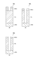
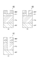
- FIG. 4A, FIG. 4B, FIG. 4C, and FIG. FIG. 4A is a partially enlarged cross-sectional view of an example substrate
- FIGS. 4B and 4C are diagrams of an example substrate in a state after execution of each of a plurality of steps of the method MT1. It is a partially expanded sectional view.
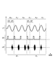
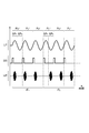
- FIG. 5 is an example timing chart related to the method MT1.
- the vertical axis indicates the first high-frequency power LF, the synchronization signal SS, and the second high-frequency power HF.
- Method MT1 includes step ST11 and step ST12.
- Step ST11 is executed in the first period P 1.
- First time length of the period P 1 of may be a time length m times the one cycle of the first high-frequency power LF. m is a natural number.
- Step ST12 is executed in the second period P 2.
- Second period P 2 is a period following the first period P 1.
- a second plasma process is performed. Duration of the second period P 2 may be a time length n times the one cycle of the first high-frequency power LF. n is a natural number.
- steps ST11 and ST12 a processing gas is supplied into the chamber 10.
- the gas supply unit GS is controlled by the control unit 80 to supply the processing gas.
- the exhaust unit 50 is controlled by the control unit 80 to set the pressure in the chamber 10 to the specified pressure.
- the pressure in the chamber 10 is set to, for example, a pressure in a range from several mTorr to 1000 mTorr.
- the first high-frequency power LF is continuously supplied to the lower electrode 18. That is, in the method MT1, the first high-frequency power LF is continuously fed to the first period P 1 and the second lower electrode 18 over a period P 2.
- the first high-frequency power supply unit 61 is controlled by the control unit 80 in order to supply the first high-frequency power LF to the lower electrode 18.
- the second high frequency power HF as pulsed RF power lower in the first within the first period P 1 of the inside part period SP 1 and the second inner portions period SP 2 in the second period P 2 It is supplied to the electrode 18 (or the upper electrode 30). That is, the second high frequency power HF is supplied as pulsed RF power at the step ST11 first inner portion period SP 1. The second high frequency power HF is supplied as pulsed RF power at the step ST12 second inner partial periods SP 2.
- the second high-frequency power supply unit 62 is controlled by the control unit 80 to supply the second high-frequency power HF.
- the first part period SP 1 is part of a period in each cycle P LF of the first high-frequency power LF.
- the second partial periods SP 2 is a part of the period in each cycle P LF of the first high-frequency power LF, a period different from the first sub-period.
- METHOD In MT1 the first part period SP 1, within each period P LF of the first high-frequency power LF, having a first high frequency power LF is negative potential output from the first RF power supply unit 61 It is included in a period (hereinafter, referred to as a “negative voltage output period”).
- the second partial periods SP 2 for a period of time in the first high frequency power LF output from the first high-frequency power supply 61 in each period P LF of the first high-frequency power LF has a positive voltage (Hereinafter, referred to as “positive voltage output period”).
- the second high-frequency power supply unit 62 can supply pulsed high-frequency power at appropriate timing in each cycle P LF specified by the synchronization signal SS in accordance with a command from the control unit 80. Therefore, in each of the plurality of first partial period SP 1, pulsed high-frequency power can be supplied at the same relative phase with respect to the period of the first high-frequency power LF. Further, in each of the plurality of second partial periods SP 2, pulsed high-frequency power can be supplied at the same relative phase with respect to the period of the first high-frequency power LF.
- the partial period (the first partial period SP 1 or the second partial period SP 2 ) set within the negative voltage output period is the first partial period SP 1 or the second partial period SP 2 within each cycle P LF of the first high-frequency power LF. It may include the point in time when one high frequency power LF has the minimum potential. Partial period set in the positive voltage output period (first part period SP 1 and the second partial periods SP 2), the first high-frequency power LF in each period P LF of the first high-frequency power LF It may include the time point with the highest potential.
- step ST11 plasma is formed from the processing gas in the chamber 10.
- the second high-frequency power HF is supplied as pulsed high-frequency power within the negative voltage output period. Therefore, in step ST11, Vpp (peak value of the voltage) of the substrate on the support 14 is increased, and the energy of ions traveling from the plasma toward the support 14 is relatively high.
- step ST12 the second high-frequency power HF is supplied as pulsed high-frequency power within the positive voltage output period. Therefore, in step ST12, the Vpp of the substrate on the support 14 is reduced, and the energy of ions traveling from the plasma to the support 14 is relatively low.
- the substrate WA to which the method MT1 can be applied has a base region URA and a film FA.
- the film FA is provided on the base region URA.
- the substrate WA may further have a mask MKA.
- the mask MKA is provided on the film FA.
- the mask MKA is patterned so as to partially expose the film FA.
- the base region URA is formed of silicon
- the film FA is formed of silicon oxide
- the mask MKA has a multilayer structure including a photoresist film and an anti-reflection film.
- the anti-reflection film of the mask MKA is provided on the film FA.
- the anti-reflection film of the mask MKA contains silicon.
- the photoresist film of the mask MKA is provided on the anti-reflection film of the mask MKA.
- substrate WA is for a first period P 1 and the second period P 2, is disposed in the chamber 10.
- the substrate WA is placed on a support 14 in the chamber 10.
- the processing gas used in step ST11 and step ST12 may include a fluorocarbon gas such as a C 4 F 8 gas.
- the processing gas used in step ST11 and step ST12 may further include an oxygen-containing gas such as O 2 gas and / or a rare gas such as argon gas.
- step ST11 the film FA is etched by ions from the plasma so as to expose the base region URA.
- Step ST11 is terminated when it is determined from the emission intensity obtained by the emission analyzer 54 that the etching amount of the film FA has decreased. For example, when it is determined that the emission intensity of CO acquired by the emission analyzer 54 is equal to or less than a predetermined value, the step ST11 is ended. Alternatively, the step ST11 ends after the elapse of the predetermined time.
- ions of high energy are supplied to the substrate WA, so that the film FA is etched at a high speed.
- step ST12 As shown in FIG. 4C, the film FA is over-etched.
- step ST12 ions of low energy are supplied to the substrate WA, so that the film FA can be over-etched while suppressing damage to the base region URA.
- FIG. 6 is a timing chart showing an example of the second high-frequency power as continuous high-frequency power.
- the second high-frequency power HF is supplied as one of a pulsed high-frequency power and a continuous high-frequency power in each cycle P LF in the first period P1, and the second high-frequency power is supplied in the second period.
- the power may be supplied as the other high-frequency power.
- the second high frequency power HF is in the first inner period P 1 is supplied as a pulse-like high-frequency power within a negative voltage output period, continuous in the second inner period P 2 It may be supplied as high frequency power.
- the energy of ions towards the support 14 is relatively high in the first inner period P 1, becomes relatively low in the second inner period P 2.
- the second high frequency power HF is in the first inner period P 1 is supplied as a continuous high-frequency power
- a second inner period P 2 as pulsed RF power to the positive voltage output period May be supplied.
- the energy of ions towards the support 14 is relatively high in the first inner period P 1, becomes relatively low in the second inner period P 2.
- FIG. 7 is a flowchart of a plasma processing method according to another exemplary embodiment.
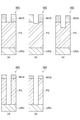
- FIG. 8A is a partially enlarged cross-sectional view of an example substrate.
- FIGS. 8B to 8E are partially enlarged cross-sectional views of an example substrate in a state after execution of each of the plurality of steps of the method MT2 shown in FIG.
- the method MT2 illustrated in FIG. 7 includes a step ST21 and a step ST22.
- Step ST21 like step ST11 way MT1 is executed in the first period P 1.
- a first plasma process is performed.
- Step ST22 like step ST12 way MT1, is performed in the second period P 2.
- Second period P 2 is a period following the first period P 1.
- a second plasma process is performed.
- Method MT2 may further include step ST23 and step ST24.
- Step ST23 is performed in the third period.
- the third period is the period following the second period P 2.
- the time length of the third period may be p times the time length of one cycle of the first high-frequency power LF. p is a natural number.
- a third plasma process is performed in step ST23.
- Step ST24 is performed in the fourth period.
- the fourth period is a period following the third period.
- the time length of the fourth period may be q times the time length of one cycle of the first high-frequency power LF. q is a natural number.
- a fourth plasma process is performed.
- a processing gas is supplied into the chamber 10.
- the gas supply unit GS is controlled by the control unit 80 to supply the processing gas.
- the exhaust unit 50 is controlled by the control unit 80 to set the pressure in the chamber 10 to the specified pressure.
- the pressure in the chamber 10 is set to, for example, a pressure in a range from several mTorr to 1000 mTorr.
- the first high-frequency power LF is continuously supplied to the lower electrode 18. That is, in the method MT2, the first high-frequency power LF is continuously supplied to the lower electrode 18 for the first to fourth periods.
- the first high-frequency power supply unit 61 is controlled by the control unit 80 to supply the first high-frequency power LF to the lower electrode 18.
- the second high frequency power HF as pulsed RF power is supplied by a first inner portion period SP 1 in each of the first period P 1 and the third period. Further, the method MT2, the second high frequency power HF is a second inner partial periods SP 2 in each of the second period P 2 and the fourth period, is supplied to the lower electrode 18 (or the upper electrode 30) You. That is, the second high frequency power HF, in each of the steps ST21 and step ST23, supplied as pulsed RF power at a first inner portion period SP 1. The second high frequency power HF, in each of the steps ST22 and step ST24, supplied as a pulse-like high-frequency power in the second inner partial periods SP 2. In step ST21, step ST22, step ST23, and step ST24, the second high-frequency power supply unit 62 is controlled by the control unit 80 to supply the second high-frequency power HF.
- the first part period SP 1 is contained within the negative voltage output periods within each period P LF of the first high-frequency power LF.
- the second partial periods SP 2 is included in the positive voltage output periods within each period P LF of the first high-frequency power LF.
- steps ST21, ST22, ST23, and ST24 plasma is formed from the processing gas in the chamber 10.
- the second high-frequency power HF is supplied as pulsed high-frequency power within the negative voltage output period. Therefore, in steps ST21 and ST23, Vpp of the substrate on the support 14 is increased, and the energy of ions traveling from the plasma to the support 14 is relatively high.
- step ST22 and step ST24 the second high-frequency power HF is supplied as pulsed high-frequency power within the positive voltage output period. Therefore, in steps ST22 and ST24, the Vpp of the substrate on the support 14 is reduced, and the energy of ions traveling from the plasma toward the support 14 is relatively low.
- the substrate WB to which the method MT2 can be applied has a first film FB1 and a second film FB2.
- the first film FB1 is provided on the second film FB2.
- the substrate WB may further include a base region URB, a third film FB3, and a mask MKB.
- the third film FB3 is provided on the base region URB.
- the second film FB2 is provided on the third film FB3.
- the mask MKB is provided on the first film FB1.
- the mask MKB is patterned so as to partially expose the first film FB1.
- the base region URB is formed from silicon.
- the first film FB1 and the third film FB3 are formed from silicon oxide.
- the second film FB2 is formed from silicon nitride.
- the mask MKB is formed from a photoresist film.
- the substrate WB is placed in the chamber 10 for a first period to a fourth period.
- the substrate WB is placed on the support 14 in the chamber 10.
- Step ST21, the process gas used in the step ST22, step ST23, and step ST24 may include a fluorocarbon gas such as C 4 F 8 gas.
- the processing gas used in step ST21, step ST22, step ST23, and step ST24 may further include an oxygen-containing gas such as O 2 gas and / or a rare gas such as argon gas.
- step ST21 ions from the plasma are irradiated on the first film FB1, and the first film FB1 is etched so as to expose the second film FB2 by chemical ion etching. Is done.
- Step ST21 ends when it is determined from the emission intensity obtained by the emission analyzer 54 that the etching amount of the first film FB1 has decreased. For example, in step ST21, when it is determined that the emission intensity of CO obtained by the emission analyzer 54 is equal to or lower than a predetermined value, or when the emission intensity of CN obtained by the emission analyzer 54 is another predetermined value. If it is determined that this is the case, the process is terminated. Alternatively, the step ST21 ends after the elapse of the predetermined time.
- step ST22 ions from the plasma are irradiated on the second film FB2, and the second film FB2 is etched so as to expose the third film FB3 by chemical ion etching. Is done.
- Step ST22 ends when it is determined from the emission intensity obtained by the emission analyzer 54 that the etching amount of the second film FB2 has decreased. For example, in step ST22, when it is determined that the emission intensity of CN acquired by the emission analyzer 54 is equal to or less than a predetermined value, or when the emission intensity of CO acquired by the emission analyzer 54 is another predetermined value. If it is determined that this is the case, the process is terminated. Alternatively, the step ST22 ends after the elapse of the predetermined time.
- step ST23 ions from the plasma are irradiated on the third film FB3, and the third film FB3 is etched by chemical ion etching so as to expose the base region URB. .
- Step ST23 is terminated when it is determined from the emission intensity obtained by the emission analyzer 54 that the etching amount of the third film FB3 has decreased.
- the process ST23 is ended when it is determined that the emission intensity of CO acquired by the emission analyzer 54 is equal to or less than a predetermined value.
- the step ST23 is ended after the elapse of the predetermined time.
- the third film FB3 is over-etched.
- overetching of the third film FB3 can be performed while suppressing damage to the base region URB.
- this method MT2 it is possible to etch a multilayer film having a film that requires relatively high energy for the etching as the first film FB1, and a film that can be etched with relatively low energy as the second film FB2. It becomes. Further, between the second film FB2 and the base region URB, a multilayer film further having a film requiring relatively high energy as the third film FB3 can be etched.
- the second high-frequency power HF is supplied as one of a pulsed high-frequency power and a continuous high-frequency power in each cycle P LF in the first period P1, and in each period P LF in period P 2 of it may be supplied as the other high-frequency power. Further, in the method MT2, the second high-frequency power HF is supplied as one of the pulsed high-frequency power and the continuous high-frequency power in each cycle P LF in the third period, and the fourth high-frequency power is supplied in the fourth period. May be supplied as the other high-frequency power in each period P LF of .
- the second high-frequency power HF is supplied as pulsed high-frequency power within the negative voltage output period during the first and third periods, and is supplied as the second high-frequency power and the fourth period. During the period, it may be supplied as continuous high-frequency power. Also in this case, the energy of the ions traveling toward the support 14 is relatively high during the first period and the third period, and relatively low during the second period and the fourth period.
- the second high-frequency power HF is supplied as continuous high-frequency power during the first period and the third period, and during the second and fourth periods, the positive voltage output period It may be supplied as a pulsed high-frequency power inside. Also in this case, the energy of the ions traveling toward the support 14 is relatively high during the first period and the third period, and relatively low during the second period and the fourth period.
- FIG. 9 is a flowchart of a plasma processing method according to still another exemplary embodiment.
- FIG. 10A is a partially enlarged cross-sectional view of an example substrate.
- FIG. 10B is a partially enlarged cross-sectional view of one example of the substrate in a state after the execution of the step ST31 of the method MT3 shown in FIG.
- the method MT3 illustrated in FIG. 9 includes a step ST31 and a step ST32.
- Step ST31 like step ST11 way MT1 is executed in the first period P 1.
- a first plasma process is performed.
- Step ST32 like step ST12 way MT1, is performed in the second period P 2.
- Second period P 2 is the first or the first subsequent period to period P 1 after the period P 1.
- a second plasma process is performed.
- steps ST31 and ST32 a processing gas is supplied into the chamber 10.
- the gas supply unit GS is controlled by the control unit 80 to supply the processing gas.
- the control unit 80 controls the exhaust device 50 to set the pressure in the chamber 10 to the specified pressure.
- the first high-frequency power LF is continuously supplied to the lower electrode 18. That is, in the method MT3, the first high-frequency power LF is continuously fed to the first period P 1 and the second lower electrode 18 over a period P 2.
- the first high-frequency power supply unit 61 is controlled by the control unit 80 in order to supply the first high-frequency power LF to the lower electrode 18.
- the second high frequency power HF as pulsed RF power lower in the first within the first period P 1 of the inside part period SP 1 and the second inner portions period SP 2 in the second period P 2 It is supplied to the electrode 18 (or the upper electrode 30). That is, the second high frequency power HF is supplied as pulsed RF power at the step ST31 first inner portion period SP 1. The second high frequency power HF is supplied as pulsed RF power at the step ST32 second inner partial periods SP 2.
- the second high-frequency power supply unit 62 is controlled by the control unit 80 to supply the second high-frequency power HF.
- the first part period SP 1 is contained within the negative voltage output periods within each period P LF of the first high-frequency power LF.
- the second partial periods SP 2 is included in the positive voltage output periods within each period P LF of the first high-frequency power LF.
- step ST31 plasma is formed from the processing gas in the chamber 10.
- the second high-frequency power HF is supplied as pulsed high-frequency power within the negative voltage output period. Therefore, in step ST31, Vpp of the substrate on the support 14 is increased, and the energy of ions traveling from the plasma toward the support 14 is relatively high.
- step ST32 the second high frequency power HF is supplied as pulsed high frequency power within the positive voltage output period. Therefore, in step ST32, the Vpp of the substrate on the support 14 is reduced, and the energy of ions traveling from the plasma to the support 14 is relatively low. In step ST32, etching mainly using radicals is performed. Further, in step ST32, the energy of ions traveling toward the inner wall surface of the chamber 10, that is, the inner wall surface that defines the internal space 10s, becomes relatively high.
- the substrate WC to which the method MT3 can be applied has a base region URC and a film FC.
- the film FC is provided on the base region URC.
- the substrate WC may further have a mask MKC.
- the mask MKC is provided on the film FC.
- the mask MKC is patterned so as to partially expose the surface of the film FC.
- the base region URC is formed of TaN
- the film FC is a multilayer film including several magnetic layers
- the mask MKC is formed of silicon oxide.
- the multilayer film of the film FC is, for example, a multilayer film constituting an MRAM element portion, and includes an MTJ (Magnetic Tunnel Junction) structure.
- substrate WC in a first period P 1, is disposed in the chamber 10.
- the substrate WC is placed on the support 14 in the chamber 10.
- the processing gas used in step ST31 and step ST32 may be a mixed gas containing a rare gas such as a Cl 2 gas and an argon gas, or a mixed gas containing a CO gas and an NH 3 gas.
- step ST31 ions from plasma are irradiated to the film FC, and the film FC is etched by chemical ion etching and / or sputtering so as to expose the base region URC.
- Step ST31 is ended when it is determined from the emission intensity obtained by the emission analyzer 54 that the etching amount of the film FC has decreased.
- the step ST31 is ended after the elapse of the predetermined time.
- ions of high energy are supplied to the substrate WC, so that the film FC formed from the difficult-to-etch material can be etched.
- Method MT3 may further include step ST3a.
- Step ST3a is performed between step ST31 and step ST32.
- the substrate WC is carried out from the internal space 10s of the chamber 10. Therefore, step ST32 can be performed in a state where substrate WC is not arranged in chamber 10.
- Method MT3 may further include step ST3b.
- Step ST3b is performed between step ST3a and step ST32.
- step ST3b a dummy substrate is carried into the chamber 10. The dummy substrate is placed on the support 14. Therefore, step ST32 may be performed in a state where the dummy substrate is placed on support base 14.
- step ST31 the deposit adheres to the inner wall surface of the chamber 10.
- the deposit can be an etching by-product.
- step ST32 deposits attached to the inner wall surface of the chamber 10 are removed by chemical species such as ions and / or radicals from plasma.
- the energy of ions towards the support 14 is lowered, the energy of ions becomes higher toward the inner wall surface of the relatively chamber 10. As a result, deposits attached to the inner wall surface of the chamber 10 are efficiently removed.
- the second high-frequency power HF is supplied as one of the pulsed high-frequency power and the continuous high-frequency power in each cycle P LF in the first period P1, and in each period P LF in period P 2 of it may be supplied as the other high-frequency power.
- the second high frequency power HF is in the first inner period P 1 is supplied as a pulse-like high-frequency power within a negative voltage output period, continuous in the second inner period P 2 It may be supplied as high frequency power.
- the energy of the ions heading for the support 14 is relatively high during the first period and relatively low during the second period.
- the second high frequency power HF is in the first inner period P 1 is supplied as a continuous high-frequency power
- a second inner period P 2 pulsed RF power within the positive voltage output period It may be supplied as.
- the energy of the ions heading for the support 14 is relatively high during the first period and relatively low during the second period.
- FIG. 11 is a flowchart of a plasma processing method according to still another exemplary embodiment.
- FIG. 12A is a partially enlarged cross-sectional view of an example substrate.
- FIGS. 12B to 12D are partially enlarged cross-sectional views of an example substrate in a state after execution of each of the plurality of steps of the method MT4 shown in FIG.
- the method MT4 shown in FIG. 11 includes a step ST41 and a step ST42.
- Step ST41 like step ST11 way MT1 is executed in the first period P 1.
- the first period P 1 may be a period having a time length of the same and time length of a single period P LF.
- a first plasma process is performed in step ST42.
- Step ST42 like step ST12 way MT1, is performed in the second period P 2.
- Second period P 2 is a period following the first period P 1.
- Second period P 2 may be a period having a time length of the same and time length of a single period P LF.
- a second plasma process is performed.
- step ST41 a processing gas is supplied into the chamber 10.
- step ST42 the same processing gas as the processing gas used in step ST41 or another processing gas is supplied into the chamber 10.
- the gas supply unit GS is controlled by the control unit 80.
- step ST41 and step ST42 the exhaust unit 50 is controlled by the control unit 80 to set the pressure in the chamber 10 to the specified pressure.
- the pressure in the chamber 10 is set to, for example, a pressure in a range from several mmTorr to 1000 mTorr.
- the first high-frequency power LF is continuously supplied to the lower electrode 18. That is, in the method MT4, the first high-frequency power LF is continuously fed to the first period P 1 and the second lower electrode 18 over a period P 2.
- the first high-frequency power supply unit 61 is controlled by the control unit 80 to supply the first high-frequency power LF to the lower electrode 18.
- the second high frequency power HF as pulsed RF power lower in the first within the first period P 1 of the inside part period SP 1 and the second inner portions period SP 2 in the second period P 2 It is supplied to the electrode 18 (or the upper electrode 30). That is, the second high frequency power HF is supplied as pulsed RF power at the step ST41 first inner portion period SP 1. The second high frequency power HF is supplied as pulsed RF power at the step ST42 second inner partial periods SP 2.
- the second high-frequency power supply unit 62 is controlled by the control unit 80 to supply the second high-frequency power HF.
- first partial periods SP 1 is contained within the negative voltage output periods within each period P LF of the first high-frequency power LF.
- the second partial periods SP 2 is included in the positive voltage output periods within each period P LF of the first high-frequency power LF.
- step ST41 plasma is formed in the chamber 10.
- the second high frequency power HF is supplied as pulsed high frequency power within the negative voltage output period. Therefore, in step ST41, the Vpp of the substrate on the support 14 is increased, and the energy of ions traveling from the plasma to the support 14 is relatively high.
- step ST42 the second high-frequency power HF is supplied as pulsed high-frequency power within the positive voltage output period. Therefore, in step ST42, the Vpp of the substrate on the support 14 is reduced, and the energy of ions traveling from the plasma toward the support 14 is relatively low.
- substrate for a first period P 1 and the second period P 2 is disposed in the chamber 10.
- the substrate is placed on a support 14 in the chamber 10.
- the substrate WD to which the method MT4 can be applied has a base region URD and a film FD as shown in FIG.
- the film FD is provided on the base region URD.
- the substrate WD may further have a mask MKD.
- the mask MKD is provided on the film FD.
- the mask MKD is patterned so as to partially expose the surface of the film FD.
- the underlying region URD is formed of silicon oxide
- the film FD is an organic film or a silicon oxide film
- the mask MKD has a multilayer structure including a photoresist film and an anti-reflection film.
- the anti-reflection film of the mask MKD is provided on the film FD.
- the anti-reflection film of the mask MKD contains silicon.
- the photoresist film of the mask MKD is provided on the antireflection film of the mask MKD.
- the processing gas used in the step ST41 may include an oxygen-containing gas such as an O 2 gas.
- the processing gas used in the step ST41 may further include a rare gas such as an argon gas.
- the processing gas used in the process ST41 may include a fluorocarbon gas such as a C 4 F 8 gas.
- the processing gas used in the process ST41 includes a fluorocarbon gas such as a C 4 F 8 gas, an oxygen-containing gas such as an O 2 gas, and a rare gas such as an argon gas. It may be a mixed gas.
- the processing gas used in the step ST42 may include a fluorocarbon gas such as a C 4 F 8 gas, regardless of whether the film FD is an organic film or a silicon oxide film.
- the processing gas used in the step ST42 may further include an oxygen-containing gas such as an O 2 gas and a rare gas such as an argon gas.
- step ST41 the energy of the ions traveling toward the support 14 is relatively high. Therefore, in step ST41, the film FD is irradiated with ions from the plasma, and the film FD is etched by chemical ion etching. As shown in FIG. 12B, in step ST41, the film FD is etched so as to provide a side wall surface. In step ST42, the energy of the ions traveling toward the support 14 is relatively low. In step ST42, as shown in FIG. 12C, the chemical species from the plasma forms a film of the deposit DP on the surface of the substrate WD. The film of the deposit DP is formed from carbon and / or fluorocarbon species.
- step ST43 it is determined whether or not a stop condition is satisfied.
- the stop condition may be determined based on the emission intensity of the predetermined wavelength acquired by the emission analyzer 54, and may be determined based on the sequence including the steps ST41 and ST42 or the execution time length of the repetition of the sequence. The determination may be made based on this. If it is determined in step ST43 that the stop condition is not satisfied, the sequence including step ST41 and step ST42 is executed again.
- the etching in step ST41 has anisotropy. Therefore, in step ST41, as shown in FIG.
- step ST41 the deposit DP extending on the side wall surface of the substrate WD is left.
- step ST41 the deposit DP extending on another surface (horizontal plane) of the substrate W is removed, and the film FD is further etched. If it is determined in step ST43 that the stop condition is satisfied, the method MT4 ends.
- the steps ST41 and ST42 are alternately repeated. That is, in the method MT4, the formation of the deposit DP (step ST42) and the etching of the film FD (step ST41) are performed alternately. According to the method MT4, during the etching of the film FD, the side wall surface of the film FD is protected by the deposit DP.
- FIG. 13 is a flowchart of a plasma processing method according to still another exemplary embodiment.
- FIG. 14A is a partially enlarged cross-sectional view of an example substrate.
- 14 (b) to 14 (d) are partially enlarged cross-sectional views of an example substrate in a state after execution of each of the plurality of steps of the method MT5 shown in FIG.
- the method MT5 shown in FIG. 13 includes a step ST51 and a step ST52.
- Step ST51 like step ST51 way MT1 is executed in the first period P 1.
- the first period P 1 may be a period having a time length of the same and time length of a single period P LF.
- a first plasma process is performed in step ST51.
- Step ST52 like step ST12 way MT1, is performed in the second period P 2.
- Second period P 2 is a period following the first period P 1.
- Second period P 2 may be a period having a time length of the same and time length of a single period P LF.
- a second plasma process is performed.
- step ST51 a processing gas is supplied into the chamber 10.
- step ST52 the same processing gas as the processing gas used in step ST51 or another processing gas is supplied into the chamber 10.
- the gas supply unit GS is controlled by the control unit 80.
- the control unit 80 controls the exhaust device 50 to set the pressure in the chamber 10 to the specified pressure.
- the pressure in the chamber 10 is set to, for example, a pressure in a range from several mTorr to 1000 mTorr.
- Steps ST51 and ST52 the first high-frequency power LF is continuously supplied to the lower electrode 18. That is, in the method MT5, a first high-frequency power LF is continuously fed to the first period P 1 and the second lower electrode 18 over a period P 2.
- the first high-frequency power supply unit 61 is controlled by the control unit 80 in order to supply the first high-frequency power LF to the lower electrode 18.
- the second high frequency power HF as pulsed RF power lower in the first within the first period P 1 of the inside part period SP 1 and the second inner portions period SP 2 in the second period P 2 It is supplied to the electrode 18 (or the upper electrode 30). That is, the second high frequency power HF is supplied as pulsed RF power at the step ST51 first inner portion period SP 1. The second high frequency power HF is supplied as pulsed RF power at the step ST52 second inner partial periods SP 2.
- the second high-frequency power supply unit 62 is controlled by the control unit 80 to supply the second high-frequency power HF.
- a first partial periods SP 1 is contained within the negative voltage output periods within each period P LF of the first high-frequency power LF.
- second partial periods SP 2 is included in the positive voltage output periods within each period P LF of the first high-frequency power LF.
- step ST51 plasma is formed in the chamber 10.
- the second high frequency power HF is supplied as pulsed high frequency power within the negative voltage output period. Therefore, in step ST51, Vpp of the substrate on the support 14 is increased, and the energy of ions traveling from the plasma toward the support 14 is relatively high.
- step ST52 the second high-frequency power HF is supplied as pulsed high-frequency power within the positive voltage output period. Therefore, in step ST52, Vpp (peak value of the voltage) of the substrate on the support 14 is reduced, and the energy of ions traveling from the plasma to the support 14 is relatively low.
- substrate for a first period P 1 and the second period P 2, is disposed in the chamber 10.
- the substrate is placed on a support 14 in the chamber 10.
- the substrate WE to which the method MT5 can be applied has a base region URE and a film FE as shown in FIG.
- the film FE is provided on the base region URE.
- the substrate WE may further have a mask MKE.
- the mask MKE is provided on the film FE.
- the mask MKE is patterned so as to partially expose the surface of the film FE.
- the base region URE is formed from silicon oxide
- the film FE is formed from polycrystalline silicon
- the mask MKE is formed from silicon oxide.
- the processing gas used in step ST51 may include a halogen-containing gas such as a Cl 2 gas, an HBr gas, and an SF 6 gas.
- the processing gas used in step ST51 may further include an oxygen-containing gas such as an O 2 gas.
- the processing gas may include an oxygen-containing gas such as O 2 gas.
- the processing gas used in step ST52 may further include a rare gas such as an argon gas.
- step ST51 the energy of the ions traveling toward the support 14 is relatively high. Therefore, in step ST51, the film FE is irradiated with ions from the plasma, and the film FE is etched by chemical ion etching. As shown in FIG. 14B, in step ST51, the film FE is etched so as to provide a side wall surface. In step ST52, the energy of the ions traveling toward the support 14 is relatively low. In step ST52, as shown in FIG. 14C, the etching of the film FE is suppressed, and the region including the surface of the film FE is altered to form the altered region MR. For example, the altered region MR is formed by oxidation of silicon in a region including the surface of the film FE.
- step ST53 it is determined whether or not a stop condition is satisfied.
- the stop condition may be determined based on the emission intensity of a predetermined wavelength acquired by the emission analyzer 54, and may be determined based on the sequence including the steps ST51 and ST52 or the execution time length of the repetition of the sequence. The determination may be made based on this. If it is determined in step ST53 that the stop condition is not satisfied, the sequence including steps ST51 and ST52 is executed again. If it is determined in step ST53 that the stop condition is satisfied, the method MT5 ends.
- the steps ST51 and ST52 are alternately repeated. That is, according to the method MT5, the alteration processing of the film FE (step ST52) and the etching of the film FE (step ST51) are alternately performed. In the method MT5, since the side wall surface of the film FE is altered, the etching of the side wall surface in the step ST51 is suppressed as shown in FIG.
- FIG. 15 is a flowchart of a plasma processing method according to still another exemplary embodiment.
- FIG. 16A is a partially enlarged cross-sectional view of an example substrate.
- 16B and 16C are partially enlarged cross-sectional views of an example substrate in a state after execution of each of the plurality of steps of the method MT6 shown in FIG.
- FIG. 17 is an example timing chart related to the method MT6.
- the vertical axis indicates the first high-frequency power LF, the synchronization signal SS, and the second high-frequency power HF.
- the method MT6 shown in FIG. 15 includes a step ST61 and a step ST62.
- Step ST61 like step ST11 way MT1 is executed in the first period P 1.
- a first plasma process is performed.
- Step ST62 like step ST12 way MT1, is performed in the second period P 2.
- Second period P 2 is a period following the first period P 1.
- a second plasma process is performed.
- steps ST61 and ST62 a processing gas is supplied into the chamber 10.
- the gas supply unit GS is controlled by the control unit 80 to supply the processing gas.
- the exhaust unit 50 is controlled by the control unit 80 to set the pressure in the chamber 10 to the specified pressure.
- the pressure in the chamber 10 is set to, for example, a pressure in a range from several mTorr to 1000 mTorr.
- step ST61 and step ST62 the first high-frequency power LF is continuously supplied to the lower electrode 18. That is, in the method MT2, the first high-frequency power LF is continuously fed to the lower electrode 18 first period P 1 and for a second period P 2.
- the first high-frequency power supply section 61 is controlled by the control section 80 in order to supply the first high-frequency power LF to the lower electrode 18.
- the second high frequency power HF as pulsed RF power, the first part period SP within 1 in the first period P 1, and the second partial periods SP in the second period P 2 2 , it is supplied to the lower electrode 18 (or the upper electrode 30). That is, the second high frequency power HF is, in step ST61, supplied as pulsed RF power at a first inner portion period SP 1.
- the second high frequency power HF is, in step ST62, supplied as a pulse-like high-frequency power in the second inner partial periods SP 2.
- the second high-frequency power supply unit 62 is controlled by the control unit 80 to supply the second high-frequency power HF.
- first partial periods SP 1 are included within the positive voltage output periods within each period P LF of the first high-frequency power LF.
- the second partial periods SP 2 is included in the negative voltage output periods within each period P LF of the first high-frequency power LF.
- step ST61 plasma is formed from the processing gas in the chamber 10.
- step ST61 as shown in FIG. 17, the second high frequency power HF is supplied as pulsed high frequency power within the positive voltage output period. Therefore, in step ST61, the Vpp of the substrate on the support 14 is reduced, and the energy of ions traveling from the plasma to the support 14 is relatively low.
- step ST62 the second high-frequency power HF is supplied as pulsed high-frequency power within the negative voltage output period. Therefore, in step ST62, Vpp of the substrate on the support 14 is increased, and the energy of ions traveling from the plasma toward the support 14 is relatively high.
- the substrate WF to which the method MT6 can be applied has a first film FF1 and a second film FF2.
- the first film FF1 is provided on the second film FF2.
- the substrate WF may further have a base region URF and a mask MKF.
- the second film FF2 is provided on the base region URF.
- the mask MKF is provided on the first film FF1.
- the mask MKF is patterned so as to partially expose the first film FF1.
- the underlying region URF is formed from silicon.
- the first film FF1 is an antireflection film containing silicon.
- the second film FF2 is formed from silicon oxide.
- the mask MKF is formed from a photoresist film.
- substrate WF is the first period P 1 and for a second period of time P 2, is disposed in the chamber 10.
- the substrate WF is placed on the support 14 in the chamber 10.
- the processing gas used in step ST61 and step ST62 includes a fluorocarbon gas such as CF 4 gas.
- the processing gas used in step ST61 and step ST62 may further include a rare gas such as an argon gas.
- step ST61 the first film FF1 is irradiated with ions from the plasma so as to expose the second film FF2, and the first film FF1 is etched by chemical ion etching. Etched. Step ST61 is ended when it is determined from the emission intensity obtained by the emission analyzer 54 that the etching amount of the first film FF1 has decreased. Alternatively, the step ST61 ends after the elapse of the predetermined time.
- step ST62 ions from the plasma are irradiated on the second film FF2 so as to expose the base region URF, and the second film FF2 is etched by chemical ion etching.
- the step ST62 ends when it is determined from the emission intensity obtained by the emission analyzer 54 that the etching amount of the second film FB2 has decreased. For example, when it is determined that the emission intensity of CO acquired by the emission analyzer 54 is equal to or less than the predetermined value, the step ST62 is ended. Alternatively, the step ST62 ends after the elapse of the predetermined time.
- the second high-frequency power HF is supplied as one of the pulsed high-frequency power and the continuous high-frequency power in each cycle P LF in the first period P1, and in each period P LF in period P 2 of it may be supplied as the other high-frequency power.
- the second high frequency power HF is in the first inner period P 1 is supplied as a pulse-like high-frequency power within the positive voltage output period, continuous in the second inner period P 2 It may be supplied as high frequency power.
- the energy of ions towards the support table 14, the first period P 1 in a relatively low becomes the second relatively high in the period P 2 of.
- the second high frequency power HF is in the first inner period P 1 is supplied as a continuous high-frequency power, a second inner period P 2 pulsed RF power within a negative voltage output period It may be supplied as.
- FIG. 18 is a flowchart of a plasma processing method according to still another exemplary embodiment.
- FIG. 19 is a timing chart of an example related to the method MT7 shown in FIG.
- FIG. 20A is a partially enlarged cross-sectional view of an example substrate.
- FIGS. 20B to 20E are partially enlarged cross-sectional views of an example substrate after execution of each of the plurality of steps of the method MT7.
- the method MT7 shown in FIG. 18 includes a step ST71 and a step ST72.
- Step ST71 like step ST71 way MT1 is executed in the first period P 1.
- the first period P 1 is a period having a time length of the same and time length of a single period P LF.
- the first start of the period P 1 is coincident with the beginning of the corresponding period P LF.
- Step ST72 like step ST12 way MT1, is performed in the second period P 2.
- Second period P 2 is a period following the first period P 1.
- Second period P 2 is a period having a time length of the same and time length of a single period P LF. Beginning of the second period P 2 coincides with the beginning of the corresponding period P LF.
- a second plasma process is performed.
- the steps ST71 and ST72 are alternately repeated.
- Method MT7 may further include step ST73.
- step ST73 a third plasma process is performed.
- Step ST73 is executed in the third period P 3.
- Third period P 3 is followed in the period in which alternating repetition of steps ST71 and step ST72 is carried out for a period.
- a processing gas is supplied into the chamber 10.
- the gas supply unit GS is controlled by the control unit 80 to supply the processing gas into the chamber 10.
- the exhaust unit 50 is controlled by the control unit 80 to set the pressure in the chamber 10 to the specified pressure.
- the pressure in the chamber 10 is set to, for example, a pressure in a range from several mTorr to 1000 mTorr.
- step ST71, step ST72, and step ST73 the first high-frequency power LF is continuously supplied to the lower electrode 18. That is, in the method MT7, the first high-frequency power LF is continuously fed to the first period P 1 and the second lower electrode 18 over a period P 2. Further, the method MT7, the first high-frequency power LF, even in the third period P 3, are continuously fed. In step ST71, step ST72, and step ST73, the first high-frequency power supply unit 61 is controlled by the control unit 80 to supply the first high-frequency power LF to the lower electrode 18.
- the second high frequency power HF is supplied to the lower electrode 18 (or the upper electrode 30) as pulsed high frequency power. That is, in the method MT7, the second high frequency power HF is supplied to the lower electrode 18 (or the upper electrode 30) as pulsed RF power at a first inner period P 1. Specifically, the method MT7, as shown in FIG. 19, the second high frequency power HF includes a lower electrode 18 (or the upper electrode as a pulsed high-frequency power within the positive voltage output period of the first within the period P 1 30). In step ST72, the second high frequency power HF is not supplied. That is, the second high frequency power HF is not supplied in the second inner period P 2.
- step ST73 the second high frequency power HF is supplied to the lower electrode 18 (or the upper electrode 30) as pulsed RF power within a positive voltage output period in each cycle P LF.
- step ST71, step ST72, and step ST73 the second high-frequency power supply unit 62 is controlled by the control unit 80 to supply and stop the supply of the second high-frequency power HF.
- step ST71 plasma is generated from the processing gas in the chamber 10.
- the Vpp of the substrate on the support 14 in step ST72 is higher than the Vpp of the substrate on the support 14 in step ST71.
- step ST73 the second high frequency power HF is supplied as pulsed high frequency power within the positive voltage output period. Therefore, in step ST73, the Vpp of the substrate on the support 14 is reduced, and the energy of ions traveling from the plasma to the support 14 is relatively low.
- substrate In the method MT7, substrate, over a period and the third period P 3 consisting of the first period P 1 and the second repetition period P 2, is disposed in the chamber 10.
- the substrate is placed on a support 14 in the chamber 10.
- the substrate WG to which the method MT7 can be applied has a base region URG and a film FG as shown in FIG.
- the film FG is provided on the base region URG.
- the substrate WG may further have a mask MKG.
- the mask MKG is provided on the film FG.
- the mask MKG is patterned so as to partially expose the surface of the film FG.
- the base region URG is formed from silicon
- the film FG is formed from silicon oxide
- the mask MKG has a multilayer structure including a photoresist film and an antireflection film.
- the anti-reflection film of the mask MKG is provided on the film FG.
- the anti-reflection film of the mask MKG contains silicon.
- the photoresist film of the mask MKG is provided on the antireflection film of the mask MKG.
- Process gas used in the method MT7 may include a fluorocarbon gas such as C 4 F 8 gas.
- the processing gas used in the method MT7 may further include an oxygen-containing gas such as O 2 gas and a rare gas such as argon gas.
- VVpp of substrate WD in step ST71 is lower than Vpp of substrate WD in step ST72.
- step ST71 since the film FG is etched at a relatively low etching rate, the etching amount of the film FG is small as shown in FIG.
- step ST72 since the film FG is etched at a high etching rate, the etching amount of the film FG is large as shown in FIG.
- step ST7a it is determined whether or not the stop condition is satisfied.
- step ST7a it is determined that the stop condition is satisfied when the number of executions of the sequence including step ST71 and step ST72 reaches the predetermined number. If it is determined in step ST7a that the stop condition is not satisfied, the sequence including step ST71 and step ST72 is executed again. If it is determined in step ST7a that the stop condition is satisfied, the alternate repetition of step ST71 and step ST72 ends.
- the stop condition may be determined based on the emission intensity of a predetermined wavelength acquired by the emission analyzer 54, and may be determined based on the execution time length of the repetition of the sequence including the steps ST71 and ST72. May be done.
- step ST73 the film FG is over-etched as shown in FIG.
- step ST73 ions of low energy are supplied to the substrate WG, so that the film FG can be over-etched while suppressing damage to the base region URG.
- FIG. 21 is a flowchart of a plasma processing method according to still another exemplary embodiment.
- FIG. 22 is a timing chart of an example related to the method MT8 shown in FIG.
- Method MT8 shown in FIG. 21 includes step ST81 and step ST82. Step ST81 and step ST82 are alternately repeated. Step ST82 is the same step as step ST72. Method MT8 may further include step ST8a and step ST83. Step ST8a is the same step as step ST7a. In step ST8a, it is determined whether a stop condition is satisfied. In step ST8a, it is determined that the stop condition is satisfied when the number of executions of the sequence including step ST81 and step 82 has reached a predetermined number.
- the stop condition may be determined based on the emission intensity of a predetermined wavelength acquired by the emission analyzer 54, and may be determined based on the execution time length of the repetition of the sequence including the steps ST81 and ST82. May be done. If it is determined in step ST8a that the stop condition is not satisfied, the sequence including step ST81 and step ST82 is executed again. On the other hand, if it is determined in step ST8a that the stop condition is satisfied, step ST83 is executed. Step ST83 is the same step as step ST73.
- step ST81 the second high frequency power HF is as shown in FIG. 22, is supplied to the lower electrode 18 (or the upper electrode 30) as pulsed RF power within a negative voltage output period of the first within the period P 1 You.
- the processing in step ST81 is otherwise the same as the processing in step ST71.
- the energy of the ions colliding with the substrate in step ST81 is higher than the energy of the ions colliding with the substrate on the support 14 in step ST71. Therefore, the etching rate of the film in step ST81 of method MT8 is higher than the etching rate of the same film in step ST71. Further, the Vpp of the substrate on the support 14 in step ST82 is higher than the Vpp of the substrate on the support 14 in step ST81. Therefore, the method MT8, ions from the plasma generated in the first period P 1 collides with high energy substrates on the support base 14 in the second period P 2. This method MT8 can be performed using the same processing gas as the processing gas used in the method MT7 for etching and over-etching the film FG of the substrate WG.
- the energy of ions traveling toward the support 14 is adjusted in accordance with the mode of the second high-frequency power HF. Specifically, the energy of the ions traveling toward the support 14 differs depending on whether the second high-frequency power HF is supplied. The energy of ions toward the support 14 differs depending on whether the second high-frequency power HF is supplied as pulsed high-frequency power or continuous high-frequency power. The energy of the ions heading toward the support 14 changes according to the period during which the pulsed high-frequency power is supplied from the second high-frequency power HF in each cycle P LF of the first high-frequency power LF.
- the energy of ions traveling toward the support 14 is low when the second high-frequency power HF is supplied as pulsed high-frequency power during the positive voltage output period.
- the energy of the ions heading toward the support 14 is high when the second high frequency power HF is supplied as pulsed high frequency power during the negative voltage output period.
- the minimum time length during which the above-described mode is maintained may be set to the time length of one cycle of the first high-frequency power LF. Therefore, it is possible to change the energy of ions traveling toward the support 14 at high speed.
- the plasma processing methods according to various embodiments may be performed using an inductively coupled plasma processing apparatus.
- the second high frequency power is supplied to the antenna to form an inductive magnetic field in the chamber 10.
- Reference numeral 10 chamber, 14: support base, 18: lower electrode, LF: first high frequency power, HF: second high frequency power, P 1 : first period, P 2 : second period, P LF ... cycle .
Abstract
According to a plasma processing method of an exemplary embodiment, first plasma processing is performed in a first period, and second plasma processing is performed in a second period following the first period. In the first period and the second period, a first high-frequency power for biasing is supplied to a lower electrode successively. A second high-frequency power for generating plasma may be supplied as a pulsed high-frequency power in a first partial period in each period of the first high-frequency power in the first period. The second high-frequency power may be supplied as a pulsed high-frequency power in a second partial period in each period of the first high-frequency power in the second period.
Description
本開示の例示的実施形態は、プラズマ処理方法及びプラズマ処理装置に関するものである。
The exemplary embodiment of the present disclosure relates to a plasma processing method and a plasma processing apparatus.
電子デバイスの製造ではプラズマ処理装置を用いてプラズマ処理が行われる。プラズマ処理装置は、チャンバ及び基板支持台を備える。基板支持台は、下部電極を含み、チャンバ内に設けられている。プラズマ処理においては、チャンバ内のガスを励起させるために高周波電力が供給されて、当該ガスからプラズマが生成される。
プ ラ ズ マ In the manufacture of electronic devices, plasma processing is performed using a plasma processing apparatus. The plasma processing apparatus includes a chamber and a substrate support. The substrate support includes a lower electrode and is provided in the chamber. In plasma processing, high-frequency power is supplied to excite a gas in a chamber, and plasma is generated from the gas.
プラズマ処理の実行中には、別の高周波電力が下部電極に供給され得る。別の高周波電力は、プラズマ生成用の高周波電力の周波数よりも低い周波数を有する。即ち、別の高周波電力はバイアス高周波電力である。一般的に、バイアス高周波電力は、基板支持台上に設けられた基板に衝突するイオンのエネルギーを調整するために用いられる。基板に衝突するイオンのエネルギーは、高い電力レベルを有するバイアス高周波電力が下部電極に供給されている場合には、高くなる。一方、基板に衝突するイオンのエネルギーは、低い電力レベルを有するバイアス高周波電力が下部電極に供給されている場合には、低くなる。
高周波 During the execution of the plasma processing, another high-frequency power can be supplied to the lower electrode. Another high frequency power has a lower frequency than the frequency of the high frequency power for plasma generation. That is, another high frequency power is a bias high frequency power. Generally, the bias radio frequency power is used to adjust the energy of ions that collide with a substrate provided on a substrate support. The energy of the ions impinging on the substrate will be higher if a bias RF power having a higher power level is supplied to the lower electrode. On the other hand, the energy of the ions colliding with the substrate will be lower if a bias RF power having a lower power level is supplied to the lower electrode.
特許文献1には、シリコン窒化膜のエッチングのためのプラズマ処理について記載されている。特許文献1に記載された技術では、シリコン窒化膜のエッチング中にバイアス高周波電力の電力レベルが高いレベルに設定される。また、特許文献1に記載された技術では、シリコン窒化膜のエッチングによってシリコン窒化膜とシリコン酸化膜が共に露出されている状態が形成されている場合に、バイアス高周波電力の電力レベルが、高いレベルと低いレベルに交互に切り替えられる。
Patent Document 1 describes a plasma treatment for etching a silicon nitride film. In the technique described in Patent Document 1, the power level of the bias high-frequency power is set to a high level during the etching of the silicon nitride film. In the technique described in Patent Document 1, when the silicon nitride film is etched to form a state in which both the silicon nitride film and the silicon oxide film are exposed, the power level of the bias high-frequency power becomes high. And alternately to a lower level.
基板のプラズマ処理に関する技術分野においては、基板支持台に向かうイオンのエネルギーを高速に変化させることが求められる。
技術 In the technical field related to plasma processing of a substrate, it is required to rapidly change the energy of ions traveling toward the substrate support.
一つの例示的実施形態によれば、プラズマ処理方法が提供される。プラズマ処理方法は、第1の期間においてチャンバ内で第1のプラズマ処理を実行する工程と、第1の期間の後の又は第1の期間に続く第2の期間においてチャンバ内で第2のプラズマ処理を実行する工程と、を含む。第1の高周波電力が、第1のプラズマ処理を実行する工程及び第2のプラズマ処理を実行する工程において、基板支持台の下部電極に連続的に供給される。第1の高周波電力は、第1の周波数を有する。基板支持台は、チャンバ内に設けられている。第2の高周波電力が、第1の期間内の第1の部分期間内及び第2の期間内の第2の部分期間内で、パルス状の高周波電力として供給される。第2の高周波電力は、第1の周波数よりも高い第2の周波数を有するプラズマ生成用の高周波電力である。第1の部分期間は、第1の高周波電力の各周期内の一部の期間である。第2の部分期間は、第1の高周波電力の各周期内の一部の期間であって、第1の部分期間とは異なる期間である。或いは、第2の高周波電力は、第1の期間内の第1の高周波電力の各周期内で、パルス状の高周波電力及び連続的な高周波電力のうち一方の高周波電力として供給され、第2の期間内の第1の高周波電力の各周期内で、他方の高周波電力として供給される。或いは、第2の高周波電力は、第1の期間内の第1の高周波電力の各周期内で、パルス状の高周波電力として供給され、第2の期間内では供給されない。
According to one exemplary embodiment, a plasma processing method is provided. The plasma processing method includes performing a first plasma process in a chamber during a first time period, and performing a second plasma process in the chamber during a second time period after the first time period or subsequent to the first time period. Performing a process. The first high frequency power is continuously supplied to the lower electrode of the substrate support in the step of performing the first plasma processing and the step of performing the second plasma processing. The first high frequency power has a first frequency. The substrate support is provided in the chamber. The second high-frequency power is supplied as pulsed high-frequency power in a first partial period of the first period and in a second partial period of the second period. The second high frequency power is a high frequency power for plasma generation having a second frequency higher than the first frequency. The first partial period is a partial period in each cycle of the first high-frequency power. The second partial period is a partial period in each cycle of the first high-frequency power and is different from the first partial period. Alternatively, the second high-frequency power is supplied as one of a pulsed high-frequency power and a continuous high-frequency power in each cycle of the first high-frequency power in the first period, and Within each period of the first high-frequency power in the period, it is supplied as the other high-frequency power. Alternatively, the second high-frequency power is supplied as pulsed high-frequency power in each cycle of the first high-frequency power in the first period, and is not supplied in the second period.
一つの例示的実施形態に係るプラズマ処理方法によれば、基板支持台に向かうイオンのエネルギーを高速に変化させることが可能である。
According to the plasma processing method according to one exemplary embodiment, it is possible to rapidly change the energy of ions traveling toward the substrate support.
以下、種々の例示的実施形態について説明する。
Hereinafter, various exemplary embodiments will be described.
一つの例示的実施形態によれば、プラズマ処理方法が提供される。プラズマ処理方法は、第1の期間においてチャンバ内で第1のプラズマ処理を実行する工程と、第1の期間の後の又は第1の期間に続く第2の期間においてチャンバ内で第2のプラズマ処理を実行する工程と、を含む。第1の高周波電力が、第1のプラズマ処理を実行する工程及び第2のプラズマ処理を実行する工程において、基板支持台の下部電極に連続的に供給される。第1の高周波電力は、第1の周波数を有する。基板支持台は、チャンバ内に設けられている。第2の高周波電力が、第1の期間内の第1の部分期間内及び第2の期間内の第2の部分期間内で、パルス状の高周波電力として供給される。第2の高周波電力は、第1の周波数よりも高い第2の周波数を有するプラズマ生成用の高周波電力である。第1の部分期間は、第1の高周波電力の各周期内の一部の期間である。第2の部分期間は、第1の高周波電力の各周期内の一部の期間であって、第1の部分期間とは異なる期間である。或いは、第2の高周波電力は、第1の期間内の第1の高周波電力の各周期内で、パルス状の高周波電力及び連続的な高周波電力のうち一方の高周波電力として供給され、第2の期間内の第1の高周波電力の各周期内で、他方の高周波電力として供給される。或いは、第2の高周波電力は、第1の期間内の第1の高周波電力の各周期内で、パルス状の高周波電力として供給され、第2の期間内では供給されない。
According to one exemplary embodiment, a plasma processing method is provided. The plasma processing method includes performing a first plasma process in a chamber during a first time period, and performing a second plasma process in the chamber during a second time period after the first time period or subsequent to the first time period. Performing a process. The first high frequency power is continuously supplied to the lower electrode of the substrate support in the step of performing the first plasma processing and the step of performing the second plasma processing. The first high frequency power has a first frequency. The substrate support is provided in the chamber. The second high-frequency power is supplied as pulsed high-frequency power in a first partial period of the first period and in a second partial period of the second period. The second high frequency power is a high frequency power for plasma generation having a second frequency higher than the first frequency. The first partial period is a partial period in each cycle of the first high-frequency power. The second partial period is a partial period in each cycle of the first high-frequency power and is different from the first partial period. Alternatively, the second high-frequency power is supplied as one of a pulsed high-frequency power and a continuous high-frequency power in each cycle of the first high-frequency power in the first period, and Within each period of the first high-frequency power in the period, it is supplied as the other high-frequency power. Alternatively, the second high-frequency power is supplied as pulsed high-frequency power in each cycle of the first high-frequency power in the first period, and is not supplied in the second period.
基板支持台に向かうイオンのエネルギーは、第2の高周波電力のモードに応じて異なる。具体的には、基板支持台に向かうイオンのエネルギーは、第2の高周波電力が供給されるか否かによって異なる。基板支持台に向かうイオンのエネルギーは、第2の高周波電力がパルス状の高周波電力として供給されるか連続的な高周波電力として供給されるか否かによって異なる。基板支持台に向かうイオンのエネルギーは、第2の高周波電力が第1の高周波電力の各周期内においてパルス状の高周波電力が供給される期間に応じて変化する。例えば、基板支持台に向かうイオンのエネルギーは、第1の高周波電源部から出力される第1の高周波電力が正の電位を有する期間内で第2の高周波電力がパルス状の高周波電力として供給される場合には、低い。また、基板支持台に向かうイオンのエネルギーは、第1の高周波電源部から出力される第1の高周波電力が負の電位を有する期間内で第2の高周波電力がパルス状の高周波電力として供給される場合には、高い。第1の例示的実施形態に係るプラズマ処理方法では、上述のモードが維持される最小の時間長が、第1の高周波電力の一周期の時間長に設定され得る。したがって、基板支持台に向かうイオンのエネルギーを高速に変化させることが可能となる。
(4) The energy of the ions traveling toward the substrate support is different depending on the mode of the second high-frequency power. Specifically, the energy of the ions heading for the substrate support differs depending on whether or not the second high-frequency power is supplied. The energy of the ions toward the substrate support depends on whether the second high frequency power is supplied as pulsed high frequency power or continuous high frequency power. The energy of the ions heading toward the substrate support changes in accordance with the period during which the pulsed high-frequency power is supplied in each cycle of the second high-frequency power and the first high-frequency power. For example, as for the energy of ions traveling toward the substrate support, the second high-frequency power is supplied as pulsed high-frequency power within a period in which the first high-frequency power output from the first high-frequency power supply has a positive potential. If it is low. The energy of the ions heading toward the substrate support is such that the second high-frequency power is supplied as pulsed high-frequency power during a period in which the first high-frequency power output from the first high-frequency power supply has a negative potential. If high. In the plasma processing method according to the first exemplary embodiment, the minimum time length during which the above-described mode is maintained may be set to the time length of one cycle of the first high-frequency power. Therefore, it is possible to change the energy of the ions traveling toward the substrate support at high speed.
第1の例示的実施形態に基づく第2の例示的実施形態において、第2の高周波電力は、第1の期間内の第1の部分期間内及び第2の期間内の第2の部分期間内でパルス状の高周波電力として供給される。第1の部分期間は、第1の高周波電力の各周期内で第1の高周波電源部から出力される第1の高周波電力が負の電位を有する期間内に含まれる。第2の部分期間は、第1の高周波電力の各周期内で第1の高周波電源部から出力される第1の高周波電力が正の電圧を有する期間内に含まれる。第2の例示的実施形態では、基板支持台に向かうイオンのエネルギーは、第1の期間内では高く、第2の期間内では低くなる。
In a second exemplary embodiment based on the first exemplary embodiment, the second high frequency power is within a first sub-period within the first period and within a second sub-period within the second period. Is supplied as pulsed high-frequency power. The first partial period is included in a period in which the first high-frequency power output from the first high-frequency power supply unit has a negative potential in each cycle of the first high-frequency power. The second partial period is included in a period in which the first high-frequency power output from the first high-frequency power supply unit has a positive voltage in each cycle of the first high-frequency power. In a second exemplary embodiment, the energy of the ions towards the substrate support is high during the first time period and low during the second time period.
第1の例示的実施形態に基づく第3の例示的実施形態において、第2の高周波電力は、第1の期間内の第1の高周波電力の各周期内で第1の高周波電源部から出力される第1の高周波電力が負の電位を有する期間において、パルス状の高周波電力として供給される。第2の高周波電力は、第2の期間内の第1の高周波電力の各周期内で連続的な高周波電力として供給される。第3の例示的実施形態では、基板支持台に向かうイオンのエネルギーは、第1の期間内では高く、第2の期間内では低くなる。
In a third exemplary embodiment based on the first exemplary embodiment, the second high-frequency power is output from the first high-frequency power supply within each period of the first high-frequency power in the first period. During the period in which the first high-frequency power has a negative potential, it is supplied as pulsed high-frequency power. The second high-frequency power is supplied as continuous high-frequency power in each cycle of the first high-frequency power in the second period. In a third exemplary embodiment, the energy of the ions towards the substrate support is high during a first time period and low during a second time period.
第1の例示的実施形態に基づく第4の例示的実施形態において、第2の高周波電力は、第1の期間内の第1の高周波電力の各周期内で連続的な高周波電力として供給される。第2の高周波電力は、第2の期間内の第1の高周波電力の各周期内で第1の高周波電源部から出力される第1の高周波電力が正の電圧を有する期間において、パルス状の高周波電力として供給される。第4の例示的実施形態では、基板支持台に向かうイオンのエネルギーは、第1の期間内では高く、第2の期間内では低くなる。
In a fourth exemplary embodiment based on the first exemplary embodiment, the second high frequency power is provided as a continuous high frequency power within each period of the first high frequency power within a first time period. . The second high-frequency power has a pulse shape during a period in which the first high-frequency power output from the first high-frequency power supply unit has a positive voltage in each cycle of the first high-frequency power in the second period. It is supplied as high frequency power. In a fourth exemplary embodiment, the energy of the ions towards the substrate support is high during the first time period and low during the second time period.
第2~第4の例示的実施形態の何れかに基づく第5の例示的実施形態において、第1の期間及び第2の期間にわたって、基板がチャンバ内に配置される。基板は、下地領域及び該下地領域上に設けられた膜を有する。第1のプラズマ処理を実行する工程において、下地領域を露出させるよう処理ガスのプラズマを用いて膜がエッチングされる。第2のプラズマ処理を実行する工程において、処理ガスのプラズマを用いて膜が更にエッチングされる。第5の例示的実施形態によれば、膜のオーバーエッチングの際にイオンのエネルギーが低減される。したがって、下地領域の損傷が抑制される。
に お い て In a fifth exemplary embodiment based on any of the second through fourth exemplary embodiments, a substrate is disposed in a chamber for a first period and a second period. The substrate has a base region and a film provided on the base region. In the step of performing the first plasma processing, the film is etched using the processing gas plasma so as to expose the underlying region. In the step of performing the second plasma processing, the film is further etched using the plasma of the processing gas. According to a fifth exemplary embodiment, the energy of the ions is reduced during overetching of the film. Therefore, damage to the underlying region is suppressed.
第2~第4の例示的実施形態の何れかに基づく第6の例示的実施形態において、第1の期間及び第2の期間にわたって、基板がチャンバ内に配置される。基板は、第1の膜及び第2の膜を有する。第1の膜は、第2の膜上に設けられている。第1のプラズマ処理を実行する工程において、処理ガスのプラズマを用いて第1の膜がエッチングされる。第2のプラズマ処理を実行する工程において、処理ガスのプラズマを用いて第2の膜がエッチングされる。第6の例示的実施形態によれば、そのエッチングに比較的高いエネルギーを要する膜を第1の膜として有し、比較的低いエネルギーでエッチングされ得る膜を第2の膜として有する多層膜のエッチングが可能となる。
に お い て In a sixth exemplary embodiment based on any of the second through fourth exemplary embodiments, a substrate is disposed in a chamber for a first period and a second period. The substrate has a first film and a second film. The first film is provided on the second film. In the step of performing the first plasma processing, the first film is etched using the plasma of the processing gas. In the step of performing the second plasma processing, the second film is etched using the plasma of the processing gas. According to the sixth exemplary embodiment, etching of a multilayer film having a film that requires relatively high energy for etching as the first film and a film that can be etched with relatively low energy as the second film Becomes possible.
第2~第4の例示的実施形態に基づく第7の例示的実施形態において、第1の期間において基板がチャンバ内に配置される。第1のプラズマ処理を実行する工程において、処理ガスのプラズマを用いて基板の膜がエッチングされる。第2の期間において基板はチャンバ内に配置されない。チャンバの内壁面に付着した堆積物が、第2のプラズマ処理を実行する工程において処理ガスのプラズマを用いて除去される。第2の期間においては、基板支持台に向かうイオンのエネルギーが低くなり、相対的にチャンバの内壁面に向かうイオンのエネルギーが高くなる。その結果、チャンバの内壁面に付着した堆積物が効率的に除去される。
7 In a seventh exemplary embodiment based on the second to fourth exemplary embodiments, a substrate is placed in a chamber during a first time period. In the step of performing the first plasma processing, the film of the substrate is etched using the plasma of the processing gas. During the second period, the substrate is not placed in the chamber. Deposits adhering to the inner wall surface of the chamber are removed using the processing gas plasma in the step of performing the second plasma processing. In the second period, the energy of ions traveling toward the substrate support becomes low, and the energy of ions traveling toward the inner wall surface of the chamber becomes relatively high. As a result, deposits attached to the inner wall surface of the chamber are efficiently removed.
第2の例示的実施形態に基づく第8の例示的実施形態において、第1の期間及び第2の期間にわたって、基板がチャンバ内に配置される。第1のプラズマ処理を実行する工程において、処理ガスのプラズマを用いて基板の膜が側壁面を提供するようにエッチングされる。第2のプラズマ処理を実行する工程において、第1のプラズマ処理を実行する工程でその膜がエッチングされた基板の表面上に、処理ガスのプラズマからの化学種又は別の処理ガスのプラズマからの化学種を含む堆積物が形成される。第1のプラズマ処理を実行する工程と第2のプラズマ処理を実行する工程とは、交互に繰り返される。第8の例示的実施形態では、堆積物の形成と膜のエッチングが交互に行われる。膜のエッチングの実行中には、膜の側壁面が堆積物によって保護される。
に In an eighth exemplary embodiment based on the second exemplary embodiment, a substrate is placed in a chamber for a first period and a second period. In performing the first plasma process, the film of the substrate is etched using the plasma of the process gas to provide a sidewall surface. In the step of performing the second plasma processing, a chemical species from the processing gas plasma or another processing gas from the plasma of the processing gas is deposited on the surface of the substrate whose film has been etched in the step of performing the first plasma processing. A deposit containing the species is formed. The step of performing the first plasma processing and the step of performing the second plasma processing are alternately repeated. In an eighth exemplary embodiment, deposit formation and film etching are alternated. During the etching of the film, the sidewall surfaces of the film are protected by the deposit.
第2の例示的実施形態に基づく第9の例示的実施形態において、第1の期間及び第2の期間にわたって、基板がチャンバ内に配置される。第1のプラズマ処理を実行する工程において、処理ガスのプラズマを用いて基板の膜が側壁面を提供するようにエッチングされる。第2のプラズマ処理を実行する工程において、第1のプラズマ処理を実行する工程でエッチングされた膜の表面を、処理ガスのプラズマ又は別の処理ガスのプラズマを用いて変質させる。第1のプラズマ処理を実行する工程と第2のプラズマ処理を実行する工程とが交互に繰り返される。第9の例示的実施形態では、膜の変質処理と膜のエッチングが交互に行われる。膜の側壁面が変質しているので、膜のエッチングの実行中に、当該側壁面のエッチングが抑制される。
に In a ninth exemplary embodiment based on the second exemplary embodiment, a substrate is placed in a chamber over a first time period and a second time period. In performing the first plasma process, the film of the substrate is etched using the plasma of the process gas to provide a sidewall surface. In the step of performing the second plasma processing, the surface of the film etched in the step of performing the first plasma processing is altered using plasma of a processing gas or another processing gas. The step of performing the first plasma processing and the step of performing the second plasma processing are alternately repeated. In the ninth exemplary embodiment, alteration of the film and etching of the film are performed alternately. Since the side wall surface of the film is altered, the etching of the side wall surface is suppressed during the etching of the film.
第1の例示的実施形態に基づく第10の例示的実施形態において、第2の高周波電力は、第1の期間内の第1の部分期間内及び第2の期間内の第2の部分期間内でパルス状の高周波電力として供給される。第1の部分期間は、第1の高周波電力の各周期内で第1の高周波電源部から出力される第1の高周波電力が正の電圧を有する期間内に含まれる。第2の部分期間は、第1の高周波電力の各周期内で第1の高周波電源部から出力される第1の高周波電力が負の電位を有する期間内に含まれる。第10の例示的実施形態では、基板支持台に向かうイオンのエネルギーは、第1の期間内では低く、第2の期間内では高くなる。
In a tenth exemplary embodiment based on the first exemplary embodiment, the second high frequency power is within a first sub-period within a first period and within a second sub-period within a second period. Is supplied as pulsed high-frequency power. The first partial period is included in a period in which the first high-frequency power output from the first high-frequency power supply unit has a positive voltage in each cycle of the first high-frequency power. The second partial period is included in a period in which the first high-frequency power output from the first high-frequency power supply unit has a negative potential in each cycle of the first high-frequency power. In a tenth exemplary embodiment, the energy of the ions toward the substrate support is low during the first time period and high during the second time period.
第1の例示的実施形態に基づく第11の例示的実施形態において、第2の高周波電力は、第1の期間内の第1の高周波電力の各周期内で第1の高周波電源部から出力される第1の高周波電力が正の電圧を有する期間において、パルス状の高周波電力として供給される。第2の高周波電力は、第2の期間内の第1の高周波電力の各周期内で連続的な高周波電力として供給される。第11の例示的実施形態では、基板支持台に向かうイオンのエネルギーは、第1の期間内では低く、第2の期間内では高くなる。
In an eleventh exemplary embodiment based on the first exemplary embodiment, the second high frequency power is output from the first high frequency power supply within each cycle of the first high frequency power within the first period. During a period in which the first high-frequency power has a positive voltage, it is supplied as pulsed high-frequency power. The second high-frequency power is supplied as continuous high-frequency power in each cycle of the first high-frequency power in the second period. In an eleventh exemplary embodiment, the energy of the ions toward the substrate support is low during a first time period and high during a second time period.
第1の例示的実施形態に基づく第12の例示的実施形態において、第2の高周波電力は、第1の期間内の第1の高周波電力の各周期内で連続的な高周波電力として供給される。第2の高周波電力は、第2の期間内の第1の高周波電力の各周期内で第1の高周波電源部から出力される第1の高周波電力が負の電位を有する期間において、パルス状の高周波電力として供給される。第12の例示的実施形態では、基板支持台に向かうイオンのエネルギーは、第1の期間内では低く、第2の期間内では高くなる。
In a twelfth exemplary embodiment based on the first exemplary embodiment, the second high frequency power is provided as a continuous high frequency power within each period of the first high frequency power within a first time period. . The second high-frequency power has a pulse-like shape during a period in which the first high-frequency power output from the first high-frequency power supply unit has a negative potential in each cycle of the first high-frequency power in the second period. It is supplied as high frequency power. In a twelfth exemplary embodiment, the energy of the ions toward the substrate support is low during a first time period and high during a second time period.
第10~第12の例示的実施形態の何れかに基づく第13の例示的実施形態において、第1の期間及び第2の期間にわたって、基板がチャンバ内に配置される。基板は、第1の膜及び第2の膜を有し、第1の膜は第2の膜上に設けられている。第1のプラズマ処理を実行する工程において、処理ガスのプラズマを用いて第1の膜がエッチングされる。第2のプラズマ処理を実行する工程において、処理ガスのプラズマを用いて第2の膜がエッチングされる。第13の例示的実施形態によれば、比較的低いエネルギーでエッチングされ得る膜を第1の膜として有し、そのエッチングに比較的高いエネルギーを要する膜を第2の膜として有する多層膜のエッチングが可能となる。
13 In the thirteenth exemplary embodiment based on any of the tenth to twelfth exemplary embodiments, the substrate is disposed in the chamber for a first period and a second period. The substrate has a first film and a second film, and the first film is provided over the second film. In the step of performing the first plasma processing, the first film is etched using the plasma of the processing gas. In the step of performing the second plasma processing, the second film is etched using the plasma of the processing gas. According to the thirteenth exemplary embodiment, etching of a multilayer film having a film that can be etched with relatively low energy as the first film and a film that requires relatively high energy for the etching as the second film Becomes possible.
第1の例示的実施形態に基づく第14の例示的実施形態においては、第1の期間及び第2の期間の各々は、第1の高周波電力の一周期の時間長と同じ時間長を有する。第2の高周波電力は、第1の期間内で第1の高周波電源部から出力される第1の高周波電力が負の電位を有する期間において、パルス状の高周波電力として供給される。第2の高周波電力は、第2の期間内では供給されない。チャンバ内に配置された基板の膜をエッチングするよう、第1のプラズマ処理を実行する工程及び第2のプラズマ処理を実行する工程が交互に繰り返される。第14の例示的実施形態によれば、第1の期間において生成されたイオンが第2の期間において高いエネルギーで基板に衝突する。
In the fourteenth exemplary embodiment based on the first exemplary embodiment, each of the first period and the second period has the same time length as one period of the first high-frequency power. The second high-frequency power is supplied as pulsed high-frequency power during a period in which the first high-frequency power output from the first high-frequency power supply unit has a negative potential within the first period. The second high frequency power is not supplied within the second period. The step of performing the first plasma processing and the step of performing the second plasma processing are alternately repeated so as to etch the film of the substrate disposed in the chamber. According to a fourteenth exemplary embodiment, ions generated during a first time period strike the substrate with high energy during a second time period.
第1の例示的実施形態に基づく第15の例示的実施形態においては、第1の期間及び第2の期間の各々は、第1の高周波電力の一周期の時間長と同じ時間長を有する。第2の高周波電力は、第1の期間内で第1の高周波電源部から出力される第1の高周波電力が正の電圧を有する期間において、パルス状の高周波電力として供給される。第2の高周波電力は、第2の期間内では供給されない。チャンバ内に配置された基板の膜をエッチングするよう、第1のプラズマ処理を実行する工程及び第2のプラズマ処理を実行する工程が交互に繰り返される。第15の例示的実施形態によれば、第1の期間において生成されたイオンが第2の期間において高いエネルギーで基板に衝突する。
In the fifteenth exemplary embodiment based on the first exemplary embodiment, each of the first period and the second period has the same time length as one period of the first high-frequency power. The second high-frequency power is supplied as pulsed high-frequency power during a period in which the first high-frequency power output from the first high-frequency power supply unit has a positive voltage within the first period. The second high frequency power is not supplied within the second period. The step of performing the first plasma processing and the step of performing the second plasma processing are alternately repeated so as to etch the film of the substrate disposed in the chamber. According to a fifteenth exemplary embodiment, ions generated during a first time period strike the substrate with high energy during a second time period.
別の例示的実施形態においては、プラズマ処理装置が提供される。プラズマ処理装置は、チャンバ、基板支持台、第1の高周波電源部、第2の高周波電源部、及び制御部を備える。基板支持台は、下部電極を含み、チャンバ内に設けられている。第1の高周波電源部は、第1の周波数を有する第1の高周波電力を下部電極に供給するように構成されている。第2の高周波電源部は、プラズマを生成するために第1の周波数よりも高い第2の周波数を有する第2の高周波電力を供給するように構成されている。制御部は、第1の高周波電源部及び第2の高周波電源部を制御するように構成されている。制御部は、第1の期間及び第1の期間の後の又は第1の期間に続く第2の期間において、第1の高周波電力を連続的に下部電極に供給するよう第1の高周波電源部を制御する。制御部は、第1の期間内の第1の部分期間内で、第2の高周波電力をパルス状の高周波電力として供給し、第2の期間内の第2の部分期間内で、第2の高周波電力をパルス状の高周波電力として供給するように、第2の高周波電源部を制御する。第1の部分期間は、第1の高周波電力の各周期内の一部の期間である。第2の部分期間は、第1の高周波電力の各周期内の一部の期間であり、第1の部分期間とは異なる期間である。或いは、制御部は、第1の期間内の第1の高周波電力の各周期内で、第2の高周波電力をパルス状の高周波電力及び連続的な高周波電力のうち一方の高周波電力として供給するように、第2の高周波電源部を制御する。また、制御部は、第2の期間内の第1の高周波電力の各周期内で、第2の高周波電力を他方の高周波電力として供給するように、第2の高周波電源部を制御する。或いは、制御部は、第1の期間内の第1の高周波電力の各周期内で、第2の高周波電力をパルス状の高周波電力として供給し、第2の期間内では第2の高周波電力を供給しないように、第2の高周波電源部を制御する。
In another exemplary embodiment, a plasma processing apparatus is provided. The plasma processing apparatus includes a chamber, a substrate support, a first high-frequency power supply, a second high-frequency power supply, and a controller. The substrate support includes a lower electrode and is provided in the chamber. The first high-frequency power supply unit is configured to supply a first high-frequency power having a first frequency to the lower electrode. The second high-frequency power supply is configured to supply a second high-frequency power having a second frequency higher than the first frequency to generate plasma. The control unit is configured to control the first high-frequency power supply unit and the second high-frequency power supply unit. The control unit is configured to control the first high-frequency power supply unit to continuously supply the first high-frequency power to the lower electrode in the first period and in a second period after the first period or in a second period following the first period. Control. The control unit supplies the second high-frequency power as pulsed high-frequency power in a first partial period of the first period, and supplies a second high-frequency power in a second partial period of the second period. The second high frequency power supply is controlled so as to supply the high frequency power as pulsed high frequency power. The first partial period is a partial period in each cycle of the first high-frequency power. The second partial period is a partial period within each cycle of the first high-frequency power, and is different from the first partial period. Alternatively, the control unit supplies the second high-frequency power as one of the pulsed high-frequency power and the continuous high-frequency power in each cycle of the first high-frequency power in the first period. Next, the second high-frequency power supply unit is controlled. Further, the control unit controls the second high-frequency power supply unit so as to supply the second high-frequency power as the other high-frequency power in each cycle of the first high-frequency power in the second period. Alternatively, the control unit supplies the second high-frequency power as pulsed high-frequency power in each cycle of the first high-frequency power in the first period, and supplies the second high-frequency power in the second period. The second high-frequency power supply unit is controlled so as not to be supplied.
以下、図面を参照して種々の例示的実施形態について詳細に説明する。なお、各図面において同一又は相当の部分に対しては同一の符号を附すこととする。
Hereinafter, various exemplary embodiments will be described in detail with reference to the drawings. In the drawings, the same or corresponding portions are denoted by the same reference numerals.
図1は、一つの例示的実施形態に係るプラズマ処理方法の流れ図である。図1に示すプラズマ処理方法(以下、「方法MT1」という)は、プラズマ処理装置を用いて実行される。図2は、一つの例示的実施形態に係るプラズマ処理装置を概略的に示す図である。本開示における種々の実施形態に係るプラズマ処理方法の実行には、図2に示すプラズマ処理装置が用いられ得る。
FIG. 1 is a flowchart of a plasma processing method according to one exemplary embodiment. The plasma processing method shown in FIG. 1 (hereinafter, referred to as “method MT1”) is performed using a plasma processing apparatus. FIG. 2 is a diagram schematically illustrating a plasma processing apparatus according to one exemplary embodiment. The plasma processing apparatus shown in FIG. 2 can be used for performing the plasma processing method according to various embodiments of the present disclosure.
図2に示すプラズマ処理装置1Aは、容量結合型のプラズマ処理装置である。プラズマ処理装置1Aは、チャンバ10を備えている。チャンバ10は、その中に内部空間10sを提供している。
プ ラ ズ マ The plasma processing apparatus 1A shown in FIG. 2 is a capacitively-coupled plasma processing apparatus. The plasma processing apparatus 1A includes a chamber 10. The chamber 10 provides an internal space 10s therein.
チャンバ10は、チャンバ本体12を含んでいる。チャンバ本体12は、略円筒形状を有している。内部空間10sは、チャンバ本体12の内側に提供されている。チャンバ本体12は、例えばアルミニウムから形成されている。チャンバ本体12の内壁面上には、耐腐食性を有する膜が設けられている。耐腐食性を有する膜は、酸化アルミニウム、酸化イットリウムといったセラミックから形成された膜であり得る。
The chamber 10 includes a chamber body 12. The chamber main body 12 has a substantially cylindrical shape. The internal space 10 s is provided inside the chamber main body 12. The chamber main body 12 is formed of, for example, aluminum. On the inner wall surface of the chamber main body 12, a film having corrosion resistance is provided. The film having corrosion resistance may be a film formed from a ceramic such as aluminum oxide or yttrium oxide.
チャンバ本体12の側壁には、通路12pが形成されている。基板Wは、内部空間10sとチャンバ10の外部との間で搬送されるときに、通路12pを通過する。通路12pは、ゲートバルブ12gにより開閉可能となっている。ゲートバルブ12gは、チャンバ本体12の側壁に沿って設けられている。
通路 A passage 12p is formed in the side wall of the chamber body 12. The substrate W passes through the passage 12p when transported between the internal space 10s and the outside of the chamber 10. The passage 12p can be opened and closed by a gate valve 12g. The gate valve 12g is provided along the side wall of the chamber main body 12.
チャンバ本体12の底部上には、支持部13が設けられている。支持部13は、絶縁材料から形成されている。支持部13は、略円筒形状を有している。支持部13は、内部空間10sの中で、チャンバ本体12の底部から上方に延在している。支持部13は、基板支持台、即ち支持台14を支持している。支持台14は、内部空間10sの中に設けられている。支持台14は、チャンバ10内、即ち内部空間10sの中で、基板Wを支持するように構成されている。
支持 A support 13 is provided on the bottom of the chamber body 12. The support 13 is formed from an insulating material. The support part 13 has a substantially cylindrical shape. The support portion 13 extends upward from the bottom of the chamber body 12 in the internal space 10s. The support 13 supports a substrate support, that is, a support 14. The support 14 is provided in the internal space 10s. The support base 14 is configured to support the substrate W in the chamber 10, that is, in the internal space 10s.
支持台14は、下部電極18及び静電チャック20を有している。支持台14は、電極プレート16を更に有し得る。電極プレート16は、例えばアルミニウムといった導体から形成されており、略円盤形状を有している。下部電極18は、電極プレート16上に設けられている。下部電極18は、例えばアルミニウムといった導体から形成されており、略円盤形状を有している。下部電極18は、電極プレート16に電気的に接続されている。
The support 14 has a lower electrode 18 and an electrostatic chuck 20. The support 14 may further include an electrode plate 16. The electrode plate 16 is formed of a conductor such as aluminum, for example, and has a substantially disk shape. The lower electrode 18 is provided on the electrode plate 16. The lower electrode 18 is formed of a conductor such as aluminum, and has a substantially disk shape. The lower electrode 18 is electrically connected to the electrode plate 16.
静電チャック20は、下部電極18上に設けられている。静電チャック20の上面の上には、基板Wが載置される。静電チャック20は、本体及び電極を有する。静電チャック20の本体は、略円盤形状を有し、誘電体から形成されている。静電チャック20の電極は、膜状の電極であり、静電チャック20の本体内に設けられている。静電チャック20の電極は、スイッチ20sを介して直流電源20pに接続されている。静電チャック20の電極に直流電源20pからの電圧が印加されると、静電チャック20と基板Wとの間で静電引力が発生する。発生した静電引力により、基板Wは、静電チャック20に引き付けられ、静電チャック20によって保持される。
The electrostatic chuck 20 is provided on the lower electrode 18. The substrate W is placed on the upper surface of the electrostatic chuck 20. The electrostatic chuck 20 has a main body and an electrode. The main body of the electrostatic chuck 20 has a substantially disk shape and is formed of a dielectric. The electrode of the electrostatic chuck 20 is a film-shaped electrode, and is provided in the main body of the electrostatic chuck 20. The electrode of the electrostatic chuck 20 is connected to a DC power supply 20p via a switch 20s. When a voltage from the DC power supply 20p is applied to the electrodes of the electrostatic chuck 20, an electrostatic attraction is generated between the electrostatic chuck 20 and the substrate W. The substrate W is attracted to the electrostatic chuck 20 by the generated electrostatic attraction, and is held by the electrostatic chuck 20.
下部電極18の周縁部上には、基板Wのエッジを囲むように、フォーカスリングFRが配置される。フォーカスリングFRは、基板Wに対するプラズマ処理の面内均一性を向上させるために設けられている。フォーカスリングFRは、限定されるものではないが、シリコン、炭化シリコン、又は石英から形成され得る。
(4) A focus ring FR is arranged on the periphery of the lower electrode 18 so as to surround the edge of the substrate W. The focus ring FR is provided to improve the in-plane uniformity of the plasma processing on the substrate W. The focus ring FR can be formed from, but not limited to, silicon, silicon carbide, or quartz.
下部電極18の内部には、流路18fが設けられている。流路18fには、チャンバ10の外部に設けられているチラーユニット22から配管22aを介して熱交換媒体(例えば冷媒)が供給される。流路18fに供給された熱交換媒体は、配管22bを介してチラーユニット22に戻される。プラズマ処理装置1Aでは、静電チャック20上に載置された基板Wの温度が、熱交換媒体と下部電極18との熱交換により、調整される。
流 路 A flow path 18f is provided inside the lower electrode 18. A heat exchange medium (for example, a refrigerant) is supplied to the flow path 18f from a chiller unit 22 provided outside the chamber 10 via a pipe 22a. The heat exchange medium supplied to the flow path 18f is returned to the chiller unit 22 via the pipe 22b. In the plasma processing apparatus 1A, the temperature of the substrate W mounted on the electrostatic chuck 20 is adjusted by heat exchange between the heat exchange medium and the lower electrode 18.
プラズマ処理装置1Aには、ガス供給ライン24が設けられている。ガス供給ライン24は、伝熱ガス供給機構からの伝熱ガス(例えばHeガス)を、静電チャック20の上面と基板Wの裏面との間に供給する。
ガ ス A gas supply line 24 is provided in the plasma processing apparatus 1A. The gas supply line 24 supplies the heat transfer gas (for example, He gas) from the heat transfer gas supply mechanism between the upper surface of the electrostatic chuck 20 and the back surface of the substrate W.
プラズマ処理装置1Aは、上部電極30を更に備えている。上部電極30は、支持台14の上方に設けられている。上部電極30は、部材32を介して、チャンバ本体12の上部に支持されている。部材32は、絶縁性を有する材料から形成されている。上部電極30と部材32は、チャンバ本体12の上部開口を閉じている。
The plasma processing apparatus 1A further includes an upper electrode 30. The upper electrode 30 is provided above the support base 14. The upper electrode 30 is supported on the upper part of the chamber main body 12 via a member 32. The member 32 is formed from a material having an insulating property. The upper electrode 30 and the member 32 close the upper opening of the chamber body 12.
上部電極30は、天板34及び支持体36を含み得る。天板34の下面は、内部空間10sの側の下面であり、内部空間10sを画成している。天板34は、ジュール熱の少ない低抵抗の導電体又は半導体から形成され得る。天板34には、複数のガス吐出孔34aが形成されている。複数のガス吐出孔34aは、天板34をその板厚方向に貫通している。
The upper electrode 30 may include a top plate 34 and a support 36. The lower surface of the top plate 34 is the lower surface on the side of the internal space 10s, and defines the internal space 10s. The top plate 34 may be formed of a low-resistance conductor or semiconductor having low Joule heat. A plurality of gas discharge holes 34a are formed in the top plate 34. The plurality of gas discharge holes 34a penetrate the top plate 34 in the plate thickness direction.
支持体36は、天板34を着脱自在に支持する。支持体36は、アルミニウムといった導電性材料から形成される。支持体36の内部には、ガス拡散室36aが設けられている。支持体36には、複数のガス孔36bが形成されている。複数のガス孔36bは、ガス拡散室36aから下方に延びている。複数のガス孔36bは、複数のガス吐出孔34aにそれぞれ連通している。支持体36には、ガス導入口36cが形成されている。ガス導入口36cは、ガス拡散室36aに接続している。ガス導入口36cには、ガス供給管38が接続されている。
(4) The support 36 detachably supports the top plate 34. The support 36 is formed from a conductive material such as aluminum. A gas diffusion chamber 36 a is provided inside the support 36. The support 36 has a plurality of gas holes 36b. The plurality of gas holes 36b extend downward from the gas diffusion chamber 36a. The plurality of gas holes 36b communicate with the plurality of gas discharge holes 34a, respectively. The support 36 has a gas inlet 36c formed therein. The gas inlet 36c is connected to the gas diffusion chamber 36a. A gas supply pipe 38 is connected to the gas inlet 36c.
プラズマ処理装置1Aは、ガス供給部GSを更に備えている。ガス供給部GSは、ガスソース群40、バルブ群41、流量制御器群42、及びバルブ群43を含む。ガスソース群40は、バルブ群41、流量制御器群42、及びバルブ群43を介して、ガス供給管38に接続されている。ガスソース群40は、複数のガスソースを含んでいる。複数のガスソースは、種々の実施形態の各々で利用される複数のガスのソースを含む。バルブ群41及びバルブ群43の各々は、複数の開閉バルブを含んでいる。流量制御器群42は、複数の流量制御器を含んでいる。流量制御器群42の複数の流量制御器の各々は、マスフローコントローラ又は圧力制御式の流量制御器である。ガスソース群40の複数のガスソースの各々は、バルブ群41の対応の開閉バルブ、流量制御器群42の対応の流量制御器、及びバルブ群43の対応の開閉バルブを介して、ガス供給管38に接続されている。
The plasma processing apparatus 1A further includes a gas supply unit GS. The gas supply unit GS includes a gas source group 40, a valve group 41, a flow controller group 42, and a valve group 43. The gas source group 40 is connected to the gas supply pipe 38 via a valve group 41, a flow controller group 42, and a valve group 43. The gas source group 40 includes a plurality of gas sources. The multiple gas sources include multiple gas sources utilized in each of the various embodiments. Each of the valve group 41 and the valve group 43 includes a plurality of open / close valves. The flow controller group 42 includes a plurality of flow controllers. Each of the plurality of flow controllers of the flow controller group 42 is a mass flow controller or a pressure control type flow controller. Each of the plurality of gas sources of the gas source group 40 is connected to a gas supply pipe via a corresponding open / close valve of the valve group 41, a corresponding flow controller of the flow controller group 42, and a corresponding open / close valve of the valve group 43. 38.
プラズマ処理装置1Aでは、チャンバ本体12の内壁面に沿って、シールド46が着脱自在に設けられている。シールド46は、支持部13の外周にも設けられている。シールド46は、チャンバ本体12にエッチング副生物が付着することを防止する。シールド46は、例えば、アルミニウムから形成された部材の表面に耐腐食性を有する膜を形成することにより構成される。耐腐食性を有する膜は、酸化イットリウムといったセラミックから形成された膜であり得る。
で は In the plasma processing apparatus 1A, the shield 46 is provided detachably along the inner wall surface of the chamber main body 12. The shield 46 is also provided on the outer periphery of the support 13. The shield 46 prevents the etching by-product from adhering to the chamber body 12. The shield 46 is formed by forming a film having corrosion resistance on the surface of a member formed of, for example, aluminum. The corrosion resistant film may be a film formed from a ceramic such as yttrium oxide.
支持部13とチャンバ本体12の側壁との間には、バッフルプレート48が設けられている。バッフルプレート48は、例えば、アルミニウムから形成された部材の表面に耐腐食性を有する膜を形成することにより構成される。耐腐食性を有する膜は、酸化イットリウムといったセラミックから形成された膜であり得る。バッフルプレート48には、複数の貫通孔が形成されている。バッフルプレート48の下方、且つ、チャンバ本体12の底部には、排気口12eが設けられている。排気口12eには、排気管52を介して排気装置50が接続されている。排気装置50は、圧力調整弁及びターボ分子ポンプといった真空ポンプを有している。
バ ッ A baffle plate 48 is provided between the support 13 and the side wall of the chamber body 12. The baffle plate 48 is formed by forming a film having corrosion resistance on the surface of a member formed of, for example, aluminum. The corrosion resistant film may be a film formed from a ceramic such as yttrium oxide. The baffle plate 48 has a plurality of through holes. An exhaust port 12 e is provided below the baffle plate 48 and at the bottom of the chamber body 12. An exhaust device 50 is connected to the exhaust port 12e via an exhaust pipe 52. The exhaust device 50 has a vacuum pump such as a pressure regulating valve and a turbo molecular pump.
プラズマ処理装置1Aは、発光分析器54を更に備え得る。発光分析器54は、チャンバ10の外側に設けられている。発光分析器54は、チャンバ10に形成された光学的に透明な窓部材を介して、プラズマからの光を受ける。発光分析器54は、プラズマの一以上の波長の発光強度を取得する。後述する制御部80は、発光分析器54によって取得された発光強度に基づいて工程を終了させることができる。
The plasma processing apparatus 1A may further include an emission analyzer 54. The emission analyzer 54 is provided outside the chamber 10. The emission analyzer 54 receives light from the plasma through an optically transparent window member formed in the chamber 10. The emission analyzer 54 acquires the emission intensity of one or more wavelengths of the plasma. The control unit 80 described below can end the process based on the emission intensity obtained by the emission analyzer 54.
プラズマ処理装置1Aは、第1の高周波電源部61を更に備えている。第1の高周波電源部61は、第1の高周波電力LFを出力するように構成されている。第1の高周波電力LFは、主としてイオンを基板Wに引き込むことに適した周波数を有する。第1の高周波電力LFの基本周波数である第1の周波数は、例えば50kHz~13.56MHzの範囲内の周波数である。
The plasma processing apparatus 1A further includes a first high-frequency power supply unit 61. The first high frequency power supply 61 is configured to output a first high frequency power LF. The first high frequency power LF has a frequency suitable for mainly drawing ions into the substrate W. The first frequency that is the fundamental frequency of the first high-frequency power LF is, for example, a frequency in the range of 50 kHz to 13.56 MHz.
第1の高周波電源部61は、整合器63を介して下部電極18に電気的に接続されている。整合器63は、整合回路を有している。整合器63の整合回路は、第1の高周波電源部61の負荷側(下部電極側)のインピーダンスを、第1の高周波電源部61の出力インピーダンスに整合させるよう構成されている。
The first high-frequency power supply 61 is electrically connected to the lower electrode 18 via the matching unit 63. The matching unit 63 has a matching circuit. The matching circuit of the matching unit 63 is configured to match the impedance on the load side (lower electrode side) of the first high-frequency power supply unit 61 with the output impedance of the first high-frequency power supply unit 61.
一実施形態において、プラズマ処理装置1Aは、方向性結合器65を更に備え得る。方向性結合器65は、第1の高周波電源部61と整合器63との間に設けられている。プラズマ処理装置1Aでは、方向性結合器65は、第1の高周波電源部61と同期信号発生器70との間に設けられている。方向性結合器65は、第1の高周波電力LFを分岐させて同期信号発生器70に供給する。方向性結合器65に供給された第1の高周波電力LFの大部分は整合器63に供給される。例えば、方向性結合器65の結合度は、60dBである。
In one embodiment, the plasma processing apparatus 1 </ b> A may further include a directional coupler 65. The directional coupler 65 is provided between the first high-frequency power supply unit 61 and the matching unit 63. In the plasma processing apparatus 1A, the directional coupler 65 is provided between the first high-frequency power supply unit 61 and the synchronization signal generator 70. The directional coupler 65 branches the first high-frequency power LF and supplies it to the synchronization signal generator 70. Most of the first high-frequency power LF supplied to the directional coupler 65 is supplied to the matching unit 63. For example, the degree of coupling of the directional coupler 65 is 60 dB.
同期信号発生器70は、第1の高周波電力LFから同期信号SSを発生するように構成されている。具体的に、同期信号発生器70は、方向性結合器65から第1の高周波電力LFの分岐電力を受ける。同期信号発生器70は、第1の高周波電力LFの分岐電力の電圧から同期信号SSを生成する。同期信号SSは、第1の高周波電力の各周期の開始時点を規定する同期パルスを含む。一実施形態において、同期信号発生器70は、第1の高周波電力LFの分岐電力の電圧を増幅器によって増幅して、増幅信号を出力する。増幅器から出力された増幅信号はコンパレータに入力される。同期信号発生器70のコンパレータは、増幅信号から同期クロック信号を生成する。同期信号発生器70は、同期クロック信号の立ち上がりにおいて同期パルスを含む同期信号を生成する。
The synchronization signal generator 70 is configured to generate the synchronization signal SS from the first high frequency power LF. Specifically, the synchronization signal generator 70 receives the branch power of the first high-frequency power LF from the directional coupler 65. The synchronization signal generator 70 generates a synchronization signal SS from the voltage of the branch power of the first high-frequency power LF. The synchronization signal SS includes a synchronization pulse that defines a start point of each cycle of the first high-frequency power. In one embodiment, the synchronization signal generator 70 amplifies the voltage of the branch power of the first high-frequency power LF with an amplifier and outputs an amplified signal. The amplified signal output from the amplifier is input to the comparator. The comparator of the synchronization signal generator 70 generates a synchronization clock signal from the amplified signal. The synchronization signal generator 70 generates a synchronization signal including a synchronization pulse at the rising edge of the synchronization clock signal.
プラズマ処理装置1Aは、第2の高周波電源部62を更に備えている。第2の高周波電源部62は、チャンバ10内でガスからプラズマを生成するために、第2の高周波電力HFを出力するように構成されている。第2の高周波電力HFの基本周波数である第2の周波数は、第1の周波数よりも高い。第2の周波数は、例えば27MHz~300MHzの範囲内の周波数である。
The plasma processing apparatus 1A further includes a second high-frequency power supply unit 62. The second high-frequency power supply unit 62 is configured to output a second high-frequency power HF in order to generate plasma from gas in the chamber 10. The second frequency, which is the fundamental frequency of the second high-frequency power HF, is higher than the first frequency. The second frequency is, for example, a frequency in the range of 27 MHz to 300 MHz.
第2の高周波電源部62は、整合器64を介して下部電極18に電気的に接続されている。整合器64は、整合回路を有している。整合器64の整合回路は、第2の高周波電源部62の負荷側(下部電極側)のインピーダンスを、第2の高周波電源部62の出力インピーダンスに整合させるよう構成されている。プラズマ処理装置1Aは、方向性結合器66を更に備えていてもよい。方向性結合器66は、第2の高周波電源部62と整合器64との間に設けられている。別の実施形態では、第2の高周波電源部62は、整合器64を介して上部電極30に電気的に接続されていてもよい。
The second high-frequency power supply unit 62 is electrically connected to the lower electrode 18 via the matching unit 64. The matching unit 64 has a matching circuit. The matching circuit of the matching unit 64 is configured to match the impedance on the load side (lower electrode side) of the second high-frequency power supply unit 62 with the output impedance of the second high-frequency power supply unit 62. The plasma processing apparatus 1A may further include a directional coupler 66. The directional coupler 66 is provided between the second high-frequency power supply unit 62 and the matching unit 64. In another embodiment, the second high-frequency power supply unit 62 may be electrically connected to the upper electrode 30 via the matching unit 64.
プラズマ処理装置1Aは、制御部80を更に備え得る。制御部80は、プロセッサ、メモリといった記憶部、入力装置、表示装置、信号の入出力インターフェイス等を備えるコンピュータであり得る。制御部80は、プラズマ処理装置1Aの各部を制御する。制御部80では、入力装置を用いて、オペレータがプラズマ処理装置1Aを管理するためにコマンドの入力操作等を行うことができる。また、制御部80では、表示装置により、プラズマ処理装置1Aの稼働状況を可視化して表示することができる。さらに、制御部80の記憶部には、制御プログラム及びレシピデータが格納されている。制御プログラムは、プラズマ処理装置1Aで各種処理を実行するために、制御部80のプロセッサによって実行される。制御部80のプロセッサが、制御プログラムを実行し、レシピデータに従ってプラズマ処理装置1Aの各部を制御することにより、種々の実施形態の各々のプラズマ処理方法が、プラズマ処理装置1Aで実行される。
The plasma processing apparatus 1A may further include a control unit 80. The control unit 80 may be a computer including a processor, a storage unit such as a memory, an input device, a display device, a signal input / output interface, and the like. The control unit 80 controls each unit of the plasma processing apparatus 1A. In the control unit 80, an operator can perform a command input operation or the like for managing the plasma processing apparatus 1A using the input device. In the control unit 80, the operation status of the plasma processing apparatus 1A can be visualized and displayed on the display device. Further, a control program and recipe data are stored in the storage unit of the control unit 80. The control program is executed by the processor of the control unit 80 in order to execute various processes in the plasma processing apparatus 1A. The processor of the control unit 80 executes the control program and controls each unit of the plasma processing apparatus 1A according to the recipe data, whereby each plasma processing method of various embodiments is executed by the plasma processing apparatus 1A.
第2の高周波電源部62は、制御部80からの制御信号及び同期信号発生器70からの同期信号SSに応じて、第1の高周波電力LFの各周期内で第2の高周波電力HFを生成するか、第2の高周波電力HFの出力を停止する。第1の高周波電力LFの各周期は、同期信号SSから特定される。第2の高周波電源部62は、第2の高周波電力HFをパルス状の高周波電力又は連続的な高周波電力として生成するように構成されている。パルス状の高周波電力は、ある期間内の特定の期間内でその電力レベルが増加された高周波電力である。例えば、パルス状の高周波電力の電力レベルは、ある期間内の特定の期間においてゼロよりも大きく、当該特定の期間の前後の期間ではゼロである。第1の高周波電力LFの各周期内で第2の高周波電力HFがパルス状の高周波電力として出力される期間は、制御部80からの制御信号によって指定される。
The second high-frequency power supply unit 62 generates the second high-frequency power HF in each cycle of the first high-frequency power LF according to the control signal from the control unit 80 and the synchronization signal SS from the synchronization signal generator 70. Alternatively, the output of the second high-frequency power HF is stopped. Each cycle of the first high-frequency power LF is specified from the synchronization signal SS. The second high frequency power supply unit 62 is configured to generate the second high frequency power HF as pulsed high frequency power or continuous high frequency power. The pulsed high-frequency power is high-frequency power whose power level has been increased within a specific period within a certain period. For example, the power level of the pulsed high-frequency power is greater than zero in a specific period within a certain period, and is zero in a period before and after the specific period. The period during which the second high-frequency power HF is output as pulsed high-frequency power in each cycle of the first high-frequency power LF is specified by a control signal from the control unit 80.
プラズマ処理装置1Aの第2の高周波電源部62は、高周波信号発生器62f及び増幅器62aを有する。高周波信号発生器62fは、制御部80からの制御信号及び同期信号発生器70からの同期信号SSに応じて、第1の高周波電力LFの各周期内で高周波信号を生成するか、高周波信号の出力を停止する。第1の高周波電力LFの各周期は、同期信号SSから特定される。高周波信号発生器62fによって生成される高周波信号は、第2の周波数を有する。高周波信号発生器62fは、高周波信号を、パルス状の高周波信号又は連続的な高周波信号として生成する。第1の高周波電力LFの各周期内で高周波信号がパルス状の高周波信号として出力される期間は、制御部80からの制御信号によって指定される。高周波信号発生器62fは、例えばファンクションジェネレータである。高周波信号発生器62fによって生成された高周波信号は、増幅器62aに入力される。プラズマ処理装置1Aの第2の高周波電源部62では、第2の高周波電力HFは、増幅器62aによって高周波信号が増幅されることにより生成される。
The second high-frequency power supply unit 62 of the plasma processing apparatus 1A has a high-frequency signal generator 62f and an amplifier 62a. The high-frequency signal generator 62f generates a high-frequency signal in each cycle of the first high-frequency power LF or generates a high-frequency signal according to the control signal from the control unit 80 and the synchronization signal SS from the synchronization signal generator 70. Stop output. Each cycle of the first high-frequency power LF is specified from the synchronization signal SS. The high frequency signal generated by the high frequency signal generator 62f has the second frequency. The high-frequency signal generator 62f generates a high-frequency signal as a pulsed high-frequency signal or a continuous high-frequency signal. The period during which the high-frequency signal is output as a pulsed high-frequency signal in each cycle of the first high-frequency power LF is specified by a control signal from the control unit 80. The high-frequency signal generator 62f is, for example, a function generator. The high-frequency signal generated by the high-frequency signal generator 62f is input to the amplifier 62a. In the second high-frequency power supply unit 62 of the plasma processing apparatus 1A, the second high-frequency power HF is generated by amplifying the high-frequency signal by the amplifier 62a.
種々の実施形態の各々のプラズマ処理方法は、図3に示すプラズマ処理装置を用いて実行されてもよい。図3は、別の例示的実施形態に係るプラズマ処理装置を概略的に示す図である。以下、プラズマ処理装置1Aと図3に示すプラズマ処理装置1Bとの相違点に関して、プラズマ処理装置1Bの説明を行う。プラズマ処理装置1Bでは、第1の高周波電源部61は、高周波信号発生器60f及び増幅器61aを有する。高周波信号発生器60fは、連続的な高周波信号として第1の高周波信号を生成する。第1の高周波信号は、第1の周波数を有する。高周波信号発生器60fは、例えばファンクションジェネレータである。第1の高周波信号は、増幅器61aに入力される。プラズマ処理装置1Bでは、第1の高周波電力LFは、増幅器61aによって第1の高周波信号が増幅されることにより生成される。
The respective plasma processing methods of the various embodiments may be performed using the plasma processing apparatus shown in FIG. FIG. 3 is a diagram schematically illustrating a plasma processing apparatus according to another exemplary embodiment. Hereinafter, the plasma processing apparatus 1B will be described with respect to differences between the plasma processing apparatus 1A and the plasma processing apparatus 1B shown in FIG. In the plasma processing apparatus 1B, the first high-frequency power supply unit 61 has a high-frequency signal generator 60f and an amplifier 61a. The high-frequency signal generator 60f generates a first high-frequency signal as a continuous high-frequency signal. The first high frequency signal has a first frequency. The high-frequency signal generator 60f is, for example, a function generator. The first high-frequency signal is input to the amplifier 61a. In the plasma processing apparatus 1B, the first high-frequency power LF is generated by amplifying the first high-frequency signal by the amplifier 61a.
プラズマ処理装置1Bでは、第2の高周波電源部62は、高周波信号発生器60f及び増幅器62aを有する。即ち、第2の高周波電源部62は、高周波信号発生器60fを第1の高周波電源部61と共有している。したがって、第1の高周波電源部61と第2の高周波電源部62の間では同期がとれている。高周波信号発生器60fは、第1の高周波信号に加えて第2の高周波信号を発生する。高周波信号発生器60fによって生成される第2の高周波信号は、第2の周波数を有する。
In the plasma processing apparatus 1B, the second high-frequency power supply unit 62 has a high-frequency signal generator 60f and an amplifier 62a. That is, the second high-frequency power supply unit 62 shares the high-frequency signal generator 60f with the first high-frequency power supply unit 61. Therefore, the first high-frequency power supply 61 and the second high-frequency power supply 62 are synchronized. The high frequency signal generator 60f generates a second high frequency signal in addition to the first high frequency signal. The second high-frequency signal generated by the high-frequency signal generator 60f has a second frequency.
高周波信号発生器60fは、制御部80からの制御信号に応じて、第1の高周波電力LFの各周期内で第2の高周波信号を生成するか、第2の高周波信号の出力を停止する。高周波信号発生器60fは、第1の高周波信号の各周期に対して第2の高周波信号の出力のタイミング制御を行うことができる。高周波信号発生器60f自体が第1の高周波信号を生成しているので、第1の高周波電力LFの各周期の特定のために、別途の同期信号発生器は不要である。
The high-frequency signal generator 60f generates the second high-frequency signal or stops the output of the second high-frequency signal within each cycle of the first high-frequency power LF according to the control signal from the control unit 80. The high-frequency signal generator 60f can perform timing control of the output of the second high-frequency signal for each cycle of the first high-frequency signal. Since the high-frequency signal generator 60f itself generates the first high-frequency signal, a separate synchronization signal generator is unnecessary for specifying each cycle of the first high-frequency power LF.
高周波信号発生器60fは、第2の高周波信号を、パルス状の高周波信号又は連続的な高周波信号として生成する。第1の高周波電力LFの各周期内で第2の高周波信号がパルス状の高周波信号として出力される期間は、制御部80からの制御信号によって指定される。高周波信号発生器60fによって生成された第2の高周波信号は、増幅器62aに入力される。プラズマ処理装置1Bの第2の高周波電源部62では、第2の高周波電力HFは、増幅器62aによって第2の高周波信号が増幅されることにより生成される。
The high-frequency signal generator 60f generates the second high-frequency signal as a pulsed high-frequency signal or a continuous high-frequency signal. A period during which the second high-frequency signal is output as a pulsed high-frequency signal in each cycle of the first high-frequency power LF is specified by a control signal from the control unit 80. The second high-frequency signal generated by the high-frequency signal generator 60f is input to the amplifier 62a. In the second high-frequency power supply unit 62 of the plasma processing apparatus 1B, the second high-frequency power HF is generated by amplifying the second high-frequency signal by the amplifier 62a.
以下、プラズマ処理装置1A及びプラズマ処理装置1Bのうち何れかが用いられる場合を例として、種々の実施形態に係るプラズマ処理方法について詳細に説明する。以下の説明では、図1と共に、図4の(a)、図4の(b)、図4の(c)、及び図5を参照する。図4の(a)は一例の基板の一部拡大断面図であり、図4の(b)及び図4の(c)は方法MT1の複数の工程それぞれの実行後の状態における一例の基板の一部拡大断面図である。図5は、方法MT1に関連する一例のタイミングチャートである。図5において縦軸は、第1の高周波電力LF、同期信号SS、及び第2の高周波電力HFを示している。
Hereinafter, a plasma processing method according to various embodiments will be described in detail by taking an example in which one of the plasma processing apparatus 1A and the plasma processing apparatus 1B is used. In the following description, FIG. 4A, FIG. 4B, FIG. 4C, and FIG. FIG. 4A is a partially enlarged cross-sectional view of an example substrate, and FIGS. 4B and 4C are diagrams of an example substrate in a state after execution of each of a plurality of steps of the method MT1. It is a partially expanded sectional view. FIG. 5 is an example timing chart related to the method MT1. In FIG. 5, the vertical axis indicates the first high-frequency power LF, the synchronization signal SS, and the second high-frequency power HF.
方法MT1は、工程ST11及び工程ST12を含む。工程ST11は、第1の期間P1において実行される。第1の期間P1の時間長は、第1の高周波電力LFの一周期の時間長のm倍であり得る。mは自然数である。工程ST11では、第1のプラズマ処理が実行される。工程ST12は、第2の期間P2において実行される。第2の期間P2は、第1の期間P1に続く期間である。工程ST12では、第2のプラズマ処理が実行される。第2の期間P2の時間長は、第1の高周波電力LFの一周期の時間長のn倍であり得る。nは自然数である。
Method MT1 includes step ST11 and step ST12. Step ST11 is executed in the first period P 1. First time length of the period P 1 of may be a time length m times the one cycle of the first high-frequency power LF. m is a natural number. In step ST11, a first plasma process is performed. Step ST12 is executed in the second period P 2. Second period P 2 is a period following the first period P 1. In step ST12, a second plasma process is performed. Duration of the second period P 2 may be a time length n times the one cycle of the first high-frequency power LF. n is a natural number.
工程ST11及び工程ST12では、チャンバ10内に処理ガスが供給される。工程ST11及び工程ST12では、ガス供給部GSが、処理ガスを供給するために、制御部80によって制御される。工程ST11及び工程ST12では、排気装置50が、チャンバ10内の圧力を指定された圧力に設定するよう、制御部80によって制御される。チャンバ10内の圧力は、例えば数mTorr~1000mTorrの範囲内の圧力に設定される。
In steps ST11 and ST12, a processing gas is supplied into the chamber 10. In step ST11 and step ST12, the gas supply unit GS is controlled by the control unit 80 to supply the processing gas. In step ST11 and step ST12, the exhaust unit 50 is controlled by the control unit 80 to set the pressure in the chamber 10 to the specified pressure. The pressure in the chamber 10 is set to, for example, a pressure in a range from several mTorr to 1000 mTorr.
工程ST11及び工程ST12において、第1の高周波電力LFは、下部電極18に連続的に供給される。即ち、方法MT1では、第1の高周波電力LFは、第1の期間P1及び第2の期間P2にわたって下部電極18に連続的に供給される。工程ST11及び工程ST12において、第1の高周波電源部61は、第1の高周波電力LFを下部電極18に供給するために、制御部80によって制御される。
In the steps ST11 and ST12, the first high-frequency power LF is continuously supplied to the lower electrode 18. That is, in the method MT1, the first high-frequency power LF is continuously fed to the first period P 1 and the second lower electrode 18 over a period P 2. In steps ST11 and ST12, the first high-frequency power supply unit 61 is controlled by the control unit 80 in order to supply the first high-frequency power LF to the lower electrode 18.
第2の高周波電力HFは、パルス状の高周波電力として、第1の期間P1内の第1の部分期間SP1内及び第2の期間P2内の第2の部分期間SP2内で下部電極18(又は上部電極30)に供給される。即ち、第2の高周波電力HFは、工程ST11では第1の部分期間SP1内でパルス状の高周波電力として供給される。また、第2の高周波電力HFは、工程ST12では第2の部分期間SP2内でパルス状の高周波電力として供給される。工程ST11及び工程ST12において、第2の高周波電源部62は、第2の高周波電力HFを供給するために、制御部80によって制御される。
The second high frequency power HF as pulsed RF power, lower in the first within the first period P 1 of the inside part period SP 1 and the second inner portions period SP 2 in the second period P 2 It is supplied to the electrode 18 (or the upper electrode 30). That is, the second high frequency power HF is supplied as pulsed RF power at the step ST11 first inner portion period SP 1. The second high frequency power HF is supplied as pulsed RF power at the step ST12 second inner partial periods SP 2. In step ST11 and step ST12, the second high-frequency power supply unit 62 is controlled by the control unit 80 to supply the second high-frequency power HF.
第1の部分期間SP1は、第1の高周波電力LFの各周期PLF内の一部の期間である。第2の部分期間SP2は、第1の高周波電力LFの各周期PLF内の一部の期間であり、第1の部分期間とは異なる期間である。方法MT1では、第1の部分期間SP1は、第1の高周波電力LFの各周期PLF内で、第1の高周波電源部61から出力される第1の高周波電力LFが負の電位を有する期間(以下、「負電圧出力期間」という)内に含まれる。方法MT1では、第2の部分期間SP2は、第1の高周波電力LFの各周期PLF内で第1の高周波電源部61から出力される第1の高周波電力LFが正の電圧を有する期間(以下、「正電圧出力期間」という)内に含まれる。
The first part period SP 1 is part of a period in each cycle P LF of the first high-frequency power LF. The second partial periods SP 2 is a part of the period in each cycle P LF of the first high-frequency power LF, a period different from the first sub-period. METHOD In MT1, the first part period SP 1, within each period P LF of the first high-frequency power LF, having a first high frequency power LF is negative potential output from the first RF power supply unit 61 It is included in a period (hereinafter, referred to as a “negative voltage output period”). In method MT1, the second partial periods SP 2 for a period of time in the first high frequency power LF output from the first high-frequency power supply 61 in each period P LF of the first high-frequency power LF has a positive voltage (Hereinafter, referred to as “positive voltage output period”).
なお、第2の高周波電源部62は、同期信号SSから特定される各周期PLFにおいて、制御部80からの指令により、パルス状の高周波電力を適切なタイミングで供給することができる。したがって、複数の第1の部分期間SP1のそれぞれでは、パルス状の高周波電力が、第1の高周波電力LFの周期に対して相対的に同じ位相で供給され得る。また、複数の第2の部分期間SP2のそれぞれでは、パルス状の高周波電力が、第1の高周波電力LFの周期に対して相対的に同じ位相で供給され得る。
Note that the second high-frequency power supply unit 62 can supply pulsed high-frequency power at appropriate timing in each cycle P LF specified by the synchronization signal SS in accordance with a command from the control unit 80. Therefore, in each of the plurality of first partial period SP 1, pulsed high-frequency power can be supplied at the same relative phase with respect to the period of the first high-frequency power LF. Further, in each of the plurality of second partial periods SP 2, pulsed high-frequency power can be supplied at the same relative phase with respect to the period of the first high-frequency power LF.
種々の実施形態において、負電圧出力期間内に設定される部分期間(第1の部分期間SP1又は第2の部分期間SP2)は、第1の高周波電力LFの各周期PLF内で第1の高周波電力LFが最小の電位を有する時点を含み得る。正電圧出力期間内に設定される部分期間(第1の部分期間SP1又は第2の部分期間SP2)は、第1の高周波電力LFの各周期PLF内で第1の高周波電力LFが最大の電位を有する時点を含み得る。
In various embodiments, the partial period (the first partial period SP 1 or the second partial period SP 2 ) set within the negative voltage output period is the first partial period SP 1 or the second partial period SP 2 within each cycle P LF of the first high-frequency power LF. It may include the point in time when one high frequency power LF has the minimum potential. Partial period set in the positive voltage output period (first part period SP 1 and the second partial periods SP 2), the first high-frequency power LF in each period P LF of the first high-frequency power LF It may include the time point with the highest potential.
工程ST11及び工程ST12では、チャンバ10内で処理ガスからプラズマが形成される。工程ST11では、第2の高周波電力HFは、負電圧出力期間内でパルス状の高周波電力として供給される。したがって、工程ST11では、支持台14上の基板のVpp(電圧の波高値)が高くなり、プラズマから支持台14に向かうイオンのエネルギーが比較的高くなる。
In steps ST11 and ST12, plasma is formed from the processing gas in the chamber 10. In step ST11, the second high-frequency power HF is supplied as pulsed high-frequency power within the negative voltage output period. Therefore, in step ST11, Vpp (peak value of the voltage) of the substrate on the support 14 is increased, and the energy of ions traveling from the plasma toward the support 14 is relatively high.
一方、工程ST12では、第2の高周波電力HFは、正電圧出力期間内でパルス状の高周波電力として供給される。したがって、工程ST12では、支持台14上の基板のVppが低くなり、プラズマから支持台14に向かうイオンのエネルギーが比較的低くなる。
On the other hand, in step ST12, the second high-frequency power HF is supplied as pulsed high-frequency power within the positive voltage output period. Therefore, in step ST12, the Vpp of the substrate on the support 14 is reduced, and the energy of ions traveling from the plasma to the support 14 is relatively low.
図4の(a)に示すように、方法MT1が適用され得る基板WAは、下地領域URA及び膜FAを有する。膜FAは、下地領域URA上に設けられている。基板WAは、マスクMKAを更に有し得る。マスクMKAは、膜FA上に設けられている。マスクMKAは、膜FAを部分的に露出させるようにパターニングされている。一例において、下地領域URAはシリコンから形成されており、膜FAは酸化シリコンから形成されており、マスクMKAは、フォトレジスト膜及び反射防止膜を含む多層構造を有する。マスクMKAの反射防止膜は、膜FA上に設けられている。マスクMKAの反射防止膜は、シリコンを含有する。マスクMKAのフォトレジスト膜は、マスクMKAの反射防止膜上に設けられている。
(4) As shown in FIG. 4A, the substrate WA to which the method MT1 can be applied has a base region URA and a film FA. The film FA is provided on the base region URA. The substrate WA may further have a mask MKA. The mask MKA is provided on the film FA. The mask MKA is patterned so as to partially expose the film FA. In one example, the base region URA is formed of silicon, the film FA is formed of silicon oxide, and the mask MKA has a multilayer structure including a photoresist film and an anti-reflection film. The anti-reflection film of the mask MKA is provided on the film FA. The anti-reflection film of the mask MKA contains silicon. The photoresist film of the mask MKA is provided on the anti-reflection film of the mask MKA.
方法MT1では、基板WAは、第1の期間P1及び第2の期間P2にわたって、チャンバ10内に配置される。基板WAは、チャンバ10内では、支持台14上に載置される。工程ST11及び工程ST12で用いられる処理ガスは、C4F8ガスといったフルオロカーボンガスを含み得る。工程ST11及び工程ST12で用いられる処理ガスは、O2ガスといった酸素含有ガス及び/又はアルゴンガスといった希ガスを更に含んでいてもよい。
In method MT1, substrate WA is for a first period P 1 and the second period P 2, is disposed in the chamber 10. The substrate WA is placed on a support 14 in the chamber 10. The processing gas used in step ST11 and step ST12 may include a fluorocarbon gas such as a C 4 F 8 gas. The processing gas used in step ST11 and step ST12 may further include an oxygen-containing gas such as O 2 gas and / or a rare gas such as argon gas.
図4の(b)に示すように、工程ST11では、下地領域URAを露出させるように、プラズマからのイオンによって膜FAがエッチングされる。工程ST11は、発光分析器54によって取得される発光強度から膜FAのエッチング量が減少していると判断される場合に、終了される。例えば、発光分析器54によって取得されるCOの発光強度が所定値以下であると判定される場合に、工程ST11が終了される。或いは、工程ST11は、所定時間の経過後に終了される。工程ST11では、基板WAに対して高いエネルギーのイオンが供給されるので、膜FAは高速にエッチングされる。
(4) As shown in FIG. 4B, in step ST11, the film FA is etched by ions from the plasma so as to expose the base region URA. Step ST11 is terminated when it is determined from the emission intensity obtained by the emission analyzer 54 that the etching amount of the film FA has decreased. For example, when it is determined that the emission intensity of CO acquired by the emission analyzer 54 is equal to or less than a predetermined value, the step ST11 is ended. Alternatively, the step ST11 ends after the elapse of the predetermined time. In step ST11, ions of high energy are supplied to the substrate WA, so that the film FA is etched at a high speed.
続く工程ST12では、図4の(c)に示すように、膜FAのオーバーエッチングが行われる。工程ST12では、基板WAに対して低いエネルギーのイオンが供給されるので、下地領域URAの損傷を抑制しつつ、膜FAのオーバーエッチングを行うことができる。
(4) In the subsequent step ST12, as shown in FIG. 4C, the film FA is over-etched. In step ST12, ions of low energy are supplied to the substrate WA, so that the film FA can be over-etched while suppressing damage to the base region URA.
図6を参照する。図6は、連続的な高周波電力としての第2の高周波電力の一例を示すタイミングチャートである。方法MT1において、第2の高周波電力HFは、第1の期間P1内の各周期PLFではパルス状の高周波電力及び連続的な高周波電力のうち一方の高周波電力として供給され、第2の期間P2内の各周期PLFでは他方の高周波電力として供給されてもよい。具体的に、方法MT1において、第2の高周波電力HFは、第1の期間P1内では負電圧出力期間内でパルス状の高周波電力として供給され、第2の期間P2内では連続的な高周波電力として供給されてもよい。この場合にも、支持台14に向かうイオンのエネルギーは、第1の期間P1内では比較的高く、第2の期間P2内では比較的低くなる。
Please refer to FIG. FIG. 6 is a timing chart showing an example of the second high-frequency power as continuous high-frequency power. In the method MT1, the second high-frequency power HF is supplied as one of a pulsed high-frequency power and a continuous high-frequency power in each cycle P LF in the first period P1, and the second high-frequency power is supplied in the second period. In each cycle P LF in P 2 , the power may be supplied as the other high-frequency power. Specifically, in the method MT1, the second high frequency power HF is in the first inner period P 1 is supplied as a pulse-like high-frequency power within a negative voltage output period, continuous in the second inner period P 2 It may be supplied as high frequency power. Also in this case, the energy of ions towards the support 14 is relatively high in the first inner period P 1, becomes relatively low in the second inner period P 2.
或いは、方法MT1において、第2の高周波電力HFは、第1の期間P1内では連続的な高周波電力として供給され、第2の期間P2内では正電圧出力期間にパルス状の高周波電力として供給されてもよい。この場合にも、支持台14に向かうイオンのエネルギーは、第1の期間P1内では比較的高く、第2の期間P2内では比較的低くなる。
Alternatively, the method MT1, the second high frequency power HF is in the first inner period P 1 is supplied as a continuous high-frequency power, a second inner period P 2 as pulsed RF power to the positive voltage output period May be supplied. Also in this case, the energy of ions towards the support 14 is relatively high in the first inner period P 1, becomes relatively low in the second inner period P 2.
次に、図7、図8の(a)、図8の(b)、図8の(c)、図8の(d)、及び図8の(e)を参照する。図7は、別の例示的実施形態に係るプラズマ処理方法の流れ図である。図8の(a)は、一例の基板の一部拡大断面図である。図8の(b)~図8の(e)は、図7に示す方法MT2の複数の工程それぞれの実行後の状態における一例の基板の一部拡大断面図である。
Next, FIG. 7, FIG. 8A, FIG. 8B, FIG. 8C, FIG. 8D, and FIG. 8E will be referred to. FIG. 7 is a flowchart of a plasma processing method according to another exemplary embodiment. FIG. 8A is a partially enlarged cross-sectional view of an example substrate. FIGS. 8B to 8E are partially enlarged cross-sectional views of an example substrate in a state after execution of each of the plurality of steps of the method MT2 shown in FIG.
図7に示す方法MT2は、工程ST21及び工程ST22を含む。工程ST21は、方法MT1の工程ST11と同じく、第1の期間P1において実行される。工程ST21では、第1のプラズマ処理が実行される。工程ST22は、方法MT1の工程ST12と同じく、第2の期間P2において実行される。第2の期間P2は、第1の期間P1に続く期間である。工程ST22では、第2のプラズマ処理が実行される。
The method MT2 illustrated in FIG. 7 includes a step ST21 and a step ST22. Step ST21, like step ST11 way MT1, is executed in the first period P 1. In step ST21, a first plasma process is performed. Step ST22, like step ST12 way MT1, is performed in the second period P 2. Second period P 2 is a period following the first period P 1. In step ST22, a second plasma process is performed.
方法MT2は、工程ST23及び工程ST24を更に含み得る。工程ST23は、第3の期間において実行される。第3の期間は第2の期間P2に続く期間である。第3の期間の時間長は、第1の高周波電力LFの一周期の時間長のp倍であり得る。pは自然数である。工程ST23では、第3のプラズマ処理が実行される。工程ST24は、第4の期間において実行される。第4の期間は第3の期間に続く期間である。第4の期間の時間長は、第1の高周波電力LFの一周期の時間長のq倍であり得る。qは自然数である。工程ST24では、第4のプラズマ処理が実行される。
Method MT2 may further include step ST23 and step ST24. Step ST23 is performed in the third period. The third period is the period following the second period P 2. The time length of the third period may be p times the time length of one cycle of the first high-frequency power LF. p is a natural number. In step ST23, a third plasma process is performed. Step ST24 is performed in the fourth period. The fourth period is a period following the third period. The time length of the fourth period may be q times the time length of one cycle of the first high-frequency power LF. q is a natural number. In step ST24, a fourth plasma process is performed.
工程ST21、工程ST22、工程ST23、及び工程ST24では、チャンバ10内に処理ガスが供給される。工程ST21、工程ST22、工程ST23、及び工程ST24では、ガス供給部GSが、処理ガスを供給するために、制御部80によって制御される。工程ST21、工程ST22、工程ST23、及び工程ST24では、排気装置50が、チャンバ10内の圧力を指定された圧力に設定するよう、制御部80によって制御される。チャンバ10内の圧力は、例えば数mTorr~1000mTorrの範囲内の圧力に設定される。
In steps ST21, ST22, ST23, and ST24, a processing gas is supplied into the chamber 10. In step ST21, step ST22, step ST23, and step ST24, the gas supply unit GS is controlled by the control unit 80 to supply the processing gas. In step ST21, step ST22, step ST23, and step ST24, the exhaust unit 50 is controlled by the control unit 80 to set the pressure in the chamber 10 to the specified pressure. The pressure in the chamber 10 is set to, for example, a pressure in a range from several mTorr to 1000 mTorr.
工程ST21、工程ST22、工程ST23、及び工程ST24において、第1の高周波電力LFは、下部電極18に連続的に供給される。即ち、方法MT2では、第1の高周波電力LFは、第1の期間~第4の期間にわたって下部電極18に連続的に供給される。工程ST21、工程ST22、工程ST23、及び工程ST24において、第1の高周波電源部61は、第1の高周波電力LFを下部電極18に供給するために、制御部80によって制御される。
{Circle around (1)} In the steps ST21, ST22, ST23, and ST24, the first high-frequency power LF is continuously supplied to the lower electrode 18. That is, in the method MT2, the first high-frequency power LF is continuously supplied to the lower electrode 18 for the first to fourth periods. In step ST21, step ST22, step ST23, and step ST24, the first high-frequency power supply unit 61 is controlled by the control unit 80 to supply the first high-frequency power LF to the lower electrode 18.
方法MT2では、第2の高周波電力HFは、パルス状の高周波電力として、第1の期間P1及び第3の期間の各々における第1の部分期間SP1内で供給される。また、方法MT2では、第2の高周波電力HFは、第2の期間P2及び第4の期間の各々における第2の部分期間SP2内で、下部電極18(又は上部電極30)に供給される。即ち、第2の高周波電力HFは、工程ST21及び工程ST23の各々では、第1の部分期間SP1内でパルス状の高周波電力として供給される。また、第2の高周波電力HFは、工程ST22及び工程ST24の各々では、第2の部分期間SP2内でパルス状の高周波電力として供給される。工程ST21、工程ST22、工程ST23、及び工程ST24において、第2の高周波電源部62は、第2の高周波電力HFを供給するために、制御部80によって制御される。
In method MT2, the second high frequency power HF as pulsed RF power is supplied by a first inner portion period SP 1 in each of the first period P 1 and the third period. Further, the method MT2, the second high frequency power HF is a second inner partial periods SP 2 in each of the second period P 2 and the fourth period, is supplied to the lower electrode 18 (or the upper electrode 30) You. That is, the second high frequency power HF, in each of the steps ST21 and step ST23, supplied as pulsed RF power at a first inner portion period SP 1. The second high frequency power HF, in each of the steps ST22 and step ST24, supplied as a pulse-like high-frequency power in the second inner partial periods SP 2. In step ST21, step ST22, step ST23, and step ST24, the second high-frequency power supply unit 62 is controlled by the control unit 80 to supply the second high-frequency power HF.
方法MT2では、第1の部分期間SP1は、第1の高周波電力LFの各周期PLF内の負電圧出力期間内に含まれる。方法MT2では、第2の部分期間SP2は、第1の高周波電力LFの各周期PLF内の正電圧出力期間内に含まれる。
In method MT2, the first part period SP 1 is contained within the negative voltage output periods within each period P LF of the first high-frequency power LF. In method MT2, the second partial periods SP 2 is included in the positive voltage output periods within each period P LF of the first high-frequency power LF.
工程ST21、工程ST22、工程ST23、及び工程ST24では、チャンバ10内で処理ガスからプラズマが形成される。工程ST21及び工程ST23では、第2の高周波電力HFは、負電圧出力期間内でパルス状の高周波電力として供給される。したがって、工程ST21及び工程ST23では、支持台14上の基板のVppが高くなり、プラズマから支持台14に向かうイオンのエネルギーが比較的高くなる。
In steps ST21, ST22, ST23, and ST24, plasma is formed from the processing gas in the chamber 10. In step ST21 and step ST23, the second high-frequency power HF is supplied as pulsed high-frequency power within the negative voltage output period. Therefore, in steps ST21 and ST23, Vpp of the substrate on the support 14 is increased, and the energy of ions traveling from the plasma to the support 14 is relatively high.
一方、工程ST22及び工程ST24では、第2の高周波電力HFは、正電圧出力期間内でパルス状の高周波電力として供給される。したがって、工程ST22及び工程ST24では、支持台14上の基板のVppが低くなり、プラズマから支持台14に向かうイオンのエネルギーが比較的低くなる。
On the other hand, in step ST22 and step ST24, the second high-frequency power HF is supplied as pulsed high-frequency power within the positive voltage output period. Therefore, in steps ST22 and ST24, the Vpp of the substrate on the support 14 is reduced, and the energy of ions traveling from the plasma toward the support 14 is relatively low.
図8の(a)に示すように、方法MT2が適用され得る基板WBは、第1の膜FB1、及び第2の膜FB2を有する。第1の膜FB1は、第2の膜FB2上に設けられている。基板WBは、下地領域URB、第3の膜FB3、及びマスクMKBを更に有し得る。第3の膜FB3は、下地領域URB上に設けられている。第2の膜FB2は、第3の膜FB3上に設けられている。マスクMKBは、第1の膜FB1上に設けられている。マスクMKBは、第1の膜FB1を部分的に露出させるようにパターニングされている。一例において、下地領域URBはシリコンから形成されている。第1の膜FB1及び第3の膜FB3は、酸化シリコンから形成されている。第2の膜FB2は、窒化シリコンから形成されている。マスクMKBは、フォトレジスト膜から形成されている。
基板 As shown in FIG. 8A, the substrate WB to which the method MT2 can be applied has a first film FB1 and a second film FB2. The first film FB1 is provided on the second film FB2. The substrate WB may further include a base region URB, a third film FB3, and a mask MKB. The third film FB3 is provided on the base region URB. The second film FB2 is provided on the third film FB3. The mask MKB is provided on the first film FB1. The mask MKB is patterned so as to partially expose the first film FB1. In one example, the base region URB is formed from silicon. The first film FB1 and the third film FB3 are formed from silicon oxide. The second film FB2 is formed from silicon nitride. The mask MKB is formed from a photoresist film.
方法MT2では、基板WBは、第1の期間~第4の期間にわたって、チャンバ10内に配置される。基板WBは、チャンバ10内では、支持台14上に載置される。工程ST21、工程ST22、工程ST23、及び工程ST24で用いられる処理ガスは、C4F8ガスといったフルオロカーボンガスを含み得る。工程ST21、工程ST22、工程ST23、及び工程ST24で用いられる処理ガスは、O2ガスといった酸素含有ガス及び/又はアルゴンガスといった希ガスを更に含んでいてもよい。
In the method MT2, the substrate WB is placed in the chamber 10 for a first period to a fourth period. The substrate WB is placed on the support 14 in the chamber 10. Step ST21, the process gas used in the step ST22, step ST23, and step ST24 may include a fluorocarbon gas such as C 4 F 8 gas. The processing gas used in step ST21, step ST22, step ST23, and step ST24 may further include an oxygen-containing gas such as O 2 gas and / or a rare gas such as argon gas.
図8の(b)に示すように、工程ST21では、プラズマからのイオンが第1の膜FB1に照射され、ケミカルイオンエッチングによって第2の膜FB2を露出させるように第1の膜FB1がエッチングされる。工程ST21は、発光分析器54によって取得される発光強度から第1の膜FB1のエッチング量が減少していると判断される場合に、終了される。例えば、工程ST21は、発光分析器54によって取得されるCOの発光強度が所定値以下であると判定される場合に、或いは、発光分析器54によって取得されるCNの発光強度が別の所定値以上であると判定される場合に、終了される。或いは、工程ST21は、所定時間の経過後に終了される。
As shown in FIG. 8B, in step ST21, ions from the plasma are irradiated on the first film FB1, and the first film FB1 is etched so as to expose the second film FB2 by chemical ion etching. Is done. Step ST21 ends when it is determined from the emission intensity obtained by the emission analyzer 54 that the etching amount of the first film FB1 has decreased. For example, in step ST21, when it is determined that the emission intensity of CO obtained by the emission analyzer 54 is equal to or lower than a predetermined value, or when the emission intensity of CN obtained by the emission analyzer 54 is another predetermined value. If it is determined that this is the case, the process is terminated. Alternatively, the step ST21 ends after the elapse of the predetermined time.
図8の(c)に示すように、工程ST22では、プラズマからのイオンが第2の膜FB2に照射され、ケミカルイオンエッチングによって第3の膜FB3を露出させるように第2の膜FB2がエッチングされる。工程ST22は、発光分析器54によって取得される発光強度から第2の膜FB2のエッチング量が減少していると判断される場合に、終了される。例えば、工程ST22は、発光分析器54によって取得されるCNの発光強度が所定値以下であると判定される場合に、或いは、発光分析器54によって取得されるCOの発光強度が別の所定値以上であると判定される場合に、終了される。或いは、工程ST22は、所定時間の経過後に終了される。
As shown in FIG. 8C, in step ST22, ions from the plasma are irradiated on the second film FB2, and the second film FB2 is etched so as to expose the third film FB3 by chemical ion etching. Is done. Step ST22 ends when it is determined from the emission intensity obtained by the emission analyzer 54 that the etching amount of the second film FB2 has decreased. For example, in step ST22, when it is determined that the emission intensity of CN acquired by the emission analyzer 54 is equal to or less than a predetermined value, or when the emission intensity of CO acquired by the emission analyzer 54 is another predetermined value. If it is determined that this is the case, the process is terminated. Alternatively, the step ST22 ends after the elapse of the predetermined time.
図8の(d)に示すように、工程ST23では、プラズマからのイオンが第3の膜FB3に照射され、ケミカルイオンエッチングによって下地領域URBを露出させるように第3の膜FB3がエッチングされる。工程ST23は、発光分析器54によって取得される発光強度から第3の膜FB3のエッチング量が減少していると判断される場合に、終了される。例えば、工程ST23は、発光分析器54によって取得されるCOの発光強度が所定値以下であると判定される場合に、終了される。或いは、工程ST23は、所定時間の経過後に終了される。
As shown in FIG. 8D, in step ST23, ions from the plasma are irradiated on the third film FB3, and the third film FB3 is etched by chemical ion etching so as to expose the base region URB. . Step ST23 is terminated when it is determined from the emission intensity obtained by the emission analyzer 54 that the etching amount of the third film FB3 has decreased. For example, the process ST23 is ended when it is determined that the emission intensity of CO acquired by the emission analyzer 54 is equal to or less than a predetermined value. Alternatively, the step ST23 is ended after the elapse of the predetermined time.
続く工程ST24では、図8の(e)に示すように、第3の膜FB3のオーバーエッチングが行われる。工程ST24では、基板WBに対して低いエネルギーのイオンが供給されるので、下地領域URBの損傷を抑制しつつ、第3の膜FB3のオーバーエッチングを行うことができる。
(4) In the subsequent step ST24, as shown in FIG. 8E, the third film FB3 is over-etched. In the step ST24, since ions of low energy are supplied to the substrate WB, overetching of the third film FB3 can be performed while suppressing damage to the base region URB.
この方法MT2によれば、そのエッチングに比較的高いエネルギーを要する膜を第1の膜FB1として有し、比較的低いエネルギーでエッチングされ得る膜を第2の膜FB2として有する多層膜のエッチングが可能となる。また、第2の膜FB2と下地領域URBとの間に、そのエッチングに比較的高いエネルギーを要する膜を第3の膜FB3として更に有する多層膜のエッチングが可能となる。
According to this method MT2, it is possible to etch a multilayer film having a film that requires relatively high energy for the etching as the first film FB1, and a film that can be etched with relatively low energy as the second film FB2. It becomes. Further, between the second film FB2 and the base region URB, a multilayer film further having a film requiring relatively high energy as the third film FB3 can be etched.
なお、方法MT2において、第2の高周波電力HFは、第1の期間P1内の各周期PLFではパルス状の高周波電力及び連続的な高周波電力のうち一方の高周波電力として供給され、第2の期間P2内の各周期PLFでは他方の高周波電力として供給されてもよい。また、方法MT2において、第2の高周波電力HFは、第3の期間内の各周期PLFではパルス状の高周波電力及び連続的な高周波電力のうち一方の高周波電力として供給され、第4の期間内の各周期PLFでは他方の高周波電力として供給されてもよい。
In the method MT2, the second high-frequency power HF is supplied as one of a pulsed high-frequency power and a continuous high-frequency power in each cycle P LF in the first period P1, and in each period P LF in period P 2 of it may be supplied as the other high-frequency power. Further, in the method MT2, the second high-frequency power HF is supplied as one of the pulsed high-frequency power and the continuous high-frequency power in each cycle P LF in the third period, and the fourth high-frequency power is supplied in the fourth period. May be supplied as the other high-frequency power in each period P LF of .
具体的に、方法MT2において、第2の高周波電力HFは、第1の期間及び第3の期間内では負電圧出力期間内でパルス状の高周波電力として供給され、第2の期間及び第4の期間内では連続的な高周波電力として供給されてもよい。この場合にも、支持台14に向かうイオンのエネルギーは、第1の期間及び第3の期間内では比較的高く、第2の期間及び第4の期間内では比較的低くなる。
Specifically, in the method MT2, the second high-frequency power HF is supplied as pulsed high-frequency power within the negative voltage output period during the first and third periods, and is supplied as the second high-frequency power and the fourth period. During the period, it may be supplied as continuous high-frequency power. Also in this case, the energy of the ions traveling toward the support 14 is relatively high during the first period and the third period, and relatively low during the second period and the fourth period.
或いは、方法MT2において、第2の高周波電力HFは、第1の期間及び第3の期間内では連続的な高周波電力として供給され、第2の期間及び第4の期間内では、正電圧出力期間内でパルス状の高周波電力として供給されてもよい。この場合にも、支持台14に向かうイオンのエネルギーは、第1の期間及び第3の期間内では比較的高く、第2の期間及び第4の期間内では比較的低くなる。
Alternatively, in the method MT2, the second high-frequency power HF is supplied as continuous high-frequency power during the first period and the third period, and during the second and fourth periods, the positive voltage output period It may be supplied as a pulsed high-frequency power inside. Also in this case, the energy of the ions traveling toward the support 14 is relatively high during the first period and the third period, and relatively low during the second period and the fourth period.
次に、図9、図10の(a)、及び図10の(b)を参照する。図9は、更に別の例示的実施形態に係るプラズマ処理方法の流れ図である。図10の(a)は、一例の基板の一部拡大断面図である。図10の(b)は、図9に示す方法MT3の工程ST31の実行後の状態における一例の基板の一部拡大断面図である。
Next, reference is made to FIGS. 9, 10 (a) and 10 (b). FIG. 9 is a flowchart of a plasma processing method according to still another exemplary embodiment. FIG. 10A is a partially enlarged cross-sectional view of an example substrate. FIG. 10B is a partially enlarged cross-sectional view of one example of the substrate in a state after the execution of the step ST31 of the method MT3 shown in FIG.
図9に示す方法MT3は、工程ST31及び工程ST32を含む。工程ST31は、方法MT1の工程ST11と同じく、第1の期間P1において実行される。工程ST31では、第1のプラズマ処理が実行される。工程ST32は、方法MT1の工程ST12と同じく、第2の期間P2において実行される。第2の期間P2は、第1の期間P1の後の又は第1の期間P1に続く期間である。工程ST32では、第2のプラズマ処理が実行される。
The method MT3 illustrated in FIG. 9 includes a step ST31 and a step ST32. Step ST31, like step ST11 way MT1, is executed in the first period P 1. In step ST31, a first plasma process is performed. Step ST32, like step ST12 way MT1, is performed in the second period P 2. Second period P 2 is the first or the first subsequent period to period P 1 after the period P 1. In step ST32, a second plasma process is performed.
工程ST31及び工程ST32では、チャンバ10内に処理ガスが供給される。工程ST31及び工程ST32では、ガス供給部GSが、処理ガスを供給するために、制御部80によって制御される。工程ST31及び工程ST32では、排気装置50が、チャンバ10内の圧力を指定された圧力に設定するよう、制御部80によって制御される。
In steps ST31 and ST32, a processing gas is supplied into the chamber 10. In step ST31 and step ST32, the gas supply unit GS is controlled by the control unit 80 to supply the processing gas. In step ST31 and step ST32, the control unit 80 controls the exhaust device 50 to set the pressure in the chamber 10 to the specified pressure.
工程ST31及び工程ST32において、第1の高周波電力LFは、下部電極18に連続的に供給される。即ち、方法MT3では、第1の高周波電力LFは、第1の期間P1及び第2の期間P2にわたって下部電極18に連続的に供給される。工程ST31及び工程ST32において、第1の高周波電源部61は、第1の高周波電力LFを下部電極18に供給するために、制御部80によって制御される。
In steps ST31 and ST32, the first high-frequency power LF is continuously supplied to the lower electrode 18. That is, in the method MT3, the first high-frequency power LF is continuously fed to the first period P 1 and the second lower electrode 18 over a period P 2. In steps ST31 and ST32, the first high-frequency power supply unit 61 is controlled by the control unit 80 in order to supply the first high-frequency power LF to the lower electrode 18.
第2の高周波電力HFは、パルス状の高周波電力として、第1の期間P1内の第1の部分期間SP1内及び第2の期間P2内の第2の部分期間SP2内で下部電極18(又は上部電極30)に供給される。即ち、第2の高周波電力HFは、工程ST31では第1の部分期間SP1内でパルス状の高周波電力として供給される。また、第2の高周波電力HFは、工程ST32では第2の部分期間SP2内でパルス状の高周波電力として供給される。工程ST31及び工程ST32において、第2の高周波電源部62は、第2の高周波電力HFを供給するために、制御部80によって制御される。
The second high frequency power HF as pulsed RF power, lower in the first within the first period P 1 of the inside part period SP 1 and the second inner portions period SP 2 in the second period P 2 It is supplied to the electrode 18 (or the upper electrode 30). That is, the second high frequency power HF is supplied as pulsed RF power at the step ST31 first inner portion period SP 1. The second high frequency power HF is supplied as pulsed RF power at the step ST32 second inner partial periods SP 2. In step ST31 and step ST32, the second high-frequency power supply unit 62 is controlled by the control unit 80 to supply the second high-frequency power HF.
方法MT3では、第1の部分期間SP1は、第1の高周波電力LFの各周期PLF内の負電圧出力期間内に含まれる。方法MT3では、第2の部分期間SP2は、第1の高周波電力LFの各周期PLF内の正電圧出力期間内に含まれる。
In method MT3, the first part period SP 1 is contained within the negative voltage output periods within each period P LF of the first high-frequency power LF. In method MT3, the second partial periods SP 2 is included in the positive voltage output periods within each period P LF of the first high-frequency power LF.
工程ST31及び工程ST32では、チャンバ10内で処理ガスからプラズマが形成される。工程ST31では、第2の高周波電力HFは、負電圧出力期間内でパルス状の高周波電力として供給される。したがって、工程ST31では、支持台14上の基板のVppが高くなり、プラズマから支持台14に向かうイオンのエネルギーが比較的高くなる。
In steps ST31 and ST32, plasma is formed from the processing gas in the chamber 10. In step ST31, the second high-frequency power HF is supplied as pulsed high-frequency power within the negative voltage output period. Therefore, in step ST31, Vpp of the substrate on the support 14 is increased, and the energy of ions traveling from the plasma toward the support 14 is relatively high.
一方、工程ST32では、第2の高周波電力HFは、正電圧出力期間内でパルス状の高周波電力として供給される。したがって、工程ST32では、支持台14上の基板のVppが低くなり、プラズマから支持台14に向かうイオンのエネルギーが比較的低くなる。なお、工程ST32では、ラジカルを主体とするエッチングが行われる。また、工程ST32では、チャンバ10の内壁面、即ち、内部空間10sを画成する内壁面に向かうイオンのエネルギーが相対的に高くなる。
On the other hand, in step ST32, the second high frequency power HF is supplied as pulsed high frequency power within the positive voltage output period. Therefore, in step ST32, the Vpp of the substrate on the support 14 is reduced, and the energy of ions traveling from the plasma to the support 14 is relatively low. In step ST32, etching mainly using radicals is performed. Further, in step ST32, the energy of ions traveling toward the inner wall surface of the chamber 10, that is, the inner wall surface that defines the internal space 10s, becomes relatively high.
図10の(a)に示すように、方法MT3が適用され得る基板WCは、下地領域URC及び膜FCを有する。膜FCは、下地領域URC上に設けられている。基板WCは、マスクMKCを更に有し得る。マスクMKCは、膜FC上に設けられている。マスクMKCは、膜FCの表面を部分的に露出させるように、パターニングされている。一例において、下地領域URCはTaNから形成されており、膜FCは幾つかの磁性層を含む多層膜であり、マスクMKCは、酸化シリコンから形成されている。膜FCの多層膜は、例えばMRAM素子部を構成する多層膜であり、MTJ(Magnetic Tunnel Junction)構造を含む。
基板 As shown in FIG. 10A, the substrate WC to which the method MT3 can be applied has a base region URC and a film FC. The film FC is provided on the base region URC. The substrate WC may further have a mask MKC. The mask MKC is provided on the film FC. The mask MKC is patterned so as to partially expose the surface of the film FC. In one example, the base region URC is formed of TaN, the film FC is a multilayer film including several magnetic layers, and the mask MKC is formed of silicon oxide. The multilayer film of the film FC is, for example, a multilayer film constituting an MRAM element portion, and includes an MTJ (Magnetic Tunnel Junction) structure.
方法MT1では、基板WCは、第1の期間P1において、チャンバ10内に配置される。基板WCは、チャンバ10内では、支持台14上に載置される。工程ST31及び工程ST32で用いられる処理ガスは、Cl2ガスとアルゴンガスといった希ガスを含む混合ガス、又は、COガスとNH3ガスを含む混合ガスであり得る。
In method MT1, substrate WC, in a first period P 1, is disposed in the chamber 10. The substrate WC is placed on the support 14 in the chamber 10. The processing gas used in step ST31 and step ST32 may be a mixed gas containing a rare gas such as a Cl 2 gas and an argon gas, or a mixed gas containing a CO gas and an NH 3 gas.
図10の(b)に示すように、工程ST31では、プラズマからのイオンが膜FCに照射され、ケミカルイオンエッチング及び/又はスパッタリングによって下地領域URCを露出させるように膜FCがエッチングされる。工程ST31は、発光分析器54によって取得される発光強度から膜FCのエッチング量が減少していると判断される場合に、終了される。或いは、工程ST31は、所定時間の経過後に終了される。工程ST31では、基板WCに対して高いエネルギーのイオンが供給されるので、難エッチング材料から形成された膜FCのエッチングが可能となる。
BAs shown in FIG. 10B, in step ST31, ions from plasma are irradiated to the film FC, and the film FC is etched by chemical ion etching and / or sputtering so as to expose the base region URC. Step ST31 is ended when it is determined from the emission intensity obtained by the emission analyzer 54 that the etching amount of the film FC has decreased. Alternatively, the step ST31 is ended after the elapse of the predetermined time. In the step ST31, ions of high energy are supplied to the substrate WC, so that the film FC formed from the difficult-to-etch material can be etched.
方法MT3は、工程ST3aを更に含んでいてもよい。工程ST3aは、工程ST31と工程ST32との間で実行される。工程ST3aでは、基板WCがチャンバ10の内部空間10sから搬出される。したがって、工程ST32は、基板WCがチャンバ10内に配置されていない状態で実施され得る。方法MT3は、工程ST3bを更に含んでいてもよい。工程ST3bは、工程ST3aと工程ST32との間で実行される。工程ST3bでは、ダミー基板がチャンバ10内に搬入される。ダミー基板は、支持台14上に載置される。したがって、工程ST32は、ダミー基板が支持台14上に載置されている状態で実行されてもよい。
Method MT3 may further include step ST3a. Step ST3a is performed between step ST31 and step ST32. In step ST3a, the substrate WC is carried out from the internal space 10s of the chamber 10. Therefore, step ST32 can be performed in a state where substrate WC is not arranged in chamber 10. Method MT3 may further include step ST3b. Step ST3b is performed between step ST3a and step ST32. In step ST3b, a dummy substrate is carried into the chamber 10. The dummy substrate is placed on the support 14. Therefore, step ST32 may be performed in a state where the dummy substrate is placed on support base 14.
工程ST31では、チャンバ10の内壁面に堆積物が付着する。堆積物はエッチング副生成物であり得る。工程ST32では、チャンバ10の内壁面に付着した堆積物が、プラズマからのイオン及び/又はラジカルといった化学種によって除去される。工程ST32が実行される第2の期間P2においては、支持台14に向かうイオンのエネルギーが低くなり、相対的にチャンバ10の内壁面に向かうイオンのエネルギーが高くなる。その結果、チャンバ10の内壁面に付着した堆積物が効率的に除去される。
In step ST31, the deposit adheres to the inner wall surface of the chamber 10. The deposit can be an etching by-product. In step ST32, deposits attached to the inner wall surface of the chamber 10 are removed by chemical species such as ions and / or radicals from plasma. In the second period P 2 in which step ST32 is executed, the energy of ions towards the support 14 is lowered, the energy of ions becomes higher toward the inner wall surface of the relatively chamber 10. As a result, deposits attached to the inner wall surface of the chamber 10 are efficiently removed.
なお、方法MT3において、第2の高周波電力HFは、第1の期間P1内の各周期PLFではパルス状の高周波電力及び連続的な高周波電力のうち一方の高周波電力として供給され、第2の期間P2内の各周期PLFでは他方の高周波電力として供給されてもよい。具体的に、方法MT3において、第2の高周波電力HFは、第1の期間P1内では負電圧出力期間内でパルス状の高周波電力として供給され、第2の期間P2内では連続的な高周波電力として供給されてもよい。この場合にも、支持台14に向かうイオンのエネルギーは、第1の期間内では比較的高く、第2の期間内では比較的低くなる。
In the method MT3, the second high-frequency power HF is supplied as one of the pulsed high-frequency power and the continuous high-frequency power in each cycle P LF in the first period P1, and in each period P LF in period P 2 of it may be supplied as the other high-frequency power. Specifically, in the method MT3, the second high frequency power HF is in the first inner period P 1 is supplied as a pulse-like high-frequency power within a negative voltage output period, continuous in the second inner period P 2 It may be supplied as high frequency power. Also in this case, the energy of the ions heading for the support 14 is relatively high during the first period and relatively low during the second period.
或いは、方法MT3において、第2の高周波電力HFは、第1の期間P1内では連続的な高周波電力として供給され、第2の期間P2内では正電圧出力期間内でパルス状の高周波電力として供給されてもよい。この場合にも、支持台14に向かうイオンのエネルギーは、第1の期間内では比較的高く、第2の期間内では比較的低くなる。
Alternatively, the method MT3, the second high frequency power HF is in the first inner period P 1 is supplied as a continuous high-frequency power, a second inner period P 2 pulsed RF power within the positive voltage output period It may be supplied as. Also in this case, the energy of the ions heading for the support 14 is relatively high during the first period and relatively low during the second period.
次に、図11、図12の(a)、図12の(b)、図12の(c)、及び図12の(d)を参照する。図11は、更に別の例示的実施形態に係るプラズマ処理方法の流れ図である。図12の(a)は、一例の基板の一部拡大断面図である。図12の(b)~図12の(d)は、図11に示す方法MT4の複数の工程それぞれの実行後の状態における一例の基板の一部拡大断面図である。
Next, FIG. 11, FIG. 12A, FIG. 12B, FIG. 12C, and FIG. 12D will be referred to. FIG. 11 is a flowchart of a plasma processing method according to still another exemplary embodiment. FIG. 12A is a partially enlarged cross-sectional view of an example substrate. FIGS. 12B to 12D are partially enlarged cross-sectional views of an example substrate in a state after execution of each of the plurality of steps of the method MT4 shown in FIG.
図11に示す方法MT4は、工程ST41及び工程ST42を含む。工程ST41は、方法MT1の工程ST11と同じく、第1の期間P1において実行される。第1の期間P1は単一の周期PLFの時間長と同一の時間長を有する期間であってもよい。工程ST41では、第1のプラズマ処理が実行される。工程ST42は、方法MT1の工程ST12と同じく、第2の期間P2において実行される。第2の期間P2は、第1の期間P1に続く期間である。第2の期間P2は単一の周期PLFの時間長と同一の時間長を有する期間であってもよい。工程ST42では、第2のプラズマ処理が実行される。
The method MT4 shown in FIG. 11 includes a step ST41 and a step ST42. Step ST41, like step ST11 way MT1, is executed in the first period P 1. The first period P 1 may be a period having a time length of the same and time length of a single period P LF. In step ST41, a first plasma process is performed. Step ST42, like step ST12 way MT1, is performed in the second period P 2. Second period P 2 is a period following the first period P 1. Second period P 2 may be a period having a time length of the same and time length of a single period P LF. In step ST42, a second plasma process is performed.
工程ST41では、チャンバ10内に処理ガスが供給される。工程ST42では、工程ST41で用いられる処理ガスと同じ処理ガス又は別の処理ガスが、チャンバ10内に、供給される。工程ST41及び工程ST42では、ガス供給部GSが制御部80によって制御される。工程ST41及び工程ST42では、排気装置50が、チャンバ10内の圧力を指定された圧力に設定するよう、制御部80によって制御される。チャンバ10内の圧力は、例えば数mmTorr~1000mTorrの範囲内の圧力に設定される。
In step ST41, a processing gas is supplied into the chamber 10. In step ST42, the same processing gas as the processing gas used in step ST41 or another processing gas is supplied into the chamber 10. In step ST41 and step ST42, the gas supply unit GS is controlled by the control unit 80. In step ST41 and step ST42, the exhaust unit 50 is controlled by the control unit 80 to set the pressure in the chamber 10 to the specified pressure. The pressure in the chamber 10 is set to, for example, a pressure in a range from several mmTorr to 1000 mTorr.
工程ST41及び工程ST42において、第1の高周波電力LFは、下部電極18に連続的に供給される。即ち、方法MT4では、第1の高周波電力LFは、第1の期間P1及び第2の期間P2にわたって下部電極18に連続的に供給される。工程ST41及び工程ST42において、第1の高周波電源部61は、第1の高周波電力LFを下部電極18に供給するために、制御部80によって制御される。
In steps ST41 and ST42, the first high-frequency power LF is continuously supplied to the lower electrode 18. That is, in the method MT4, the first high-frequency power LF is continuously fed to the first period P 1 and the second lower electrode 18 over a period P 2. In steps ST41 and ST42, the first high-frequency power supply unit 61 is controlled by the control unit 80 to supply the first high-frequency power LF to the lower electrode 18.
第2の高周波電力HFは、パルス状の高周波電力として、第1の期間P1内の第1の部分期間SP1内及び第2の期間P2内の第2の部分期間SP2内で下部電極18(又は上部電極30)に供給される。即ち、第2の高周波電力HFは、工程ST41では第1の部分期間SP1内でパルス状の高周波電力として供給される。また、第2の高周波電力HFは、工程ST42では第2の部分期間SP2内でパルス状の高周波電力として供給される。工程ST41及び工程ST42において、第2の高周波電源部62は、第2の高周波電力HFを供給するために、制御部80によって制御される。
The second high frequency power HF as pulsed RF power, lower in the first within the first period P 1 of the inside part period SP 1 and the second inner portions period SP 2 in the second period P 2 It is supplied to the electrode 18 (or the upper electrode 30). That is, the second high frequency power HF is supplied as pulsed RF power at the step ST41 first inner portion period SP 1. The second high frequency power HF is supplied as pulsed RF power at the step ST42 second inner partial periods SP 2. In step ST41 and step ST42, the second high-frequency power supply unit 62 is controlled by the control unit 80 to supply the second high-frequency power HF.
方法MT4では、第1の部分期間SP1は、第1の高周波電力LFの各周期PLF内の負電圧出力期間内に含まれる。方法MT4では、第2の部分期間SP2は、第1の高周波電力LFの各周期PLF内の正電圧出力期間内に含まれる。
In method MT4, first partial periods SP 1 is contained within the negative voltage output periods within each period P LF of the first high-frequency power LF. In method MT4, the second partial periods SP 2 is included in the positive voltage output periods within each period P LF of the first high-frequency power LF.
工程ST41及び工程ST42では、チャンバ10内でプラズマが形成される。工程ST41では、第2の高周波電力HFは、負電圧出力期間内でパルス状の高周波電力として供給される。したがって、工程ST41では、支持台14上の基板のVppが高くなり、プラズマから支持台14に向かうイオンのエネルギーが比較的高くなる。
プ ラ ズ マ In steps ST41 and ST42, plasma is formed in the chamber 10. In step ST41, the second high frequency power HF is supplied as pulsed high frequency power within the negative voltage output period. Therefore, in step ST41, the Vpp of the substrate on the support 14 is increased, and the energy of ions traveling from the plasma to the support 14 is relatively high.
一方、工程ST42では、第2の高周波電力HFは、正電圧出力期間内でパルス状の高周波電力として供給される。したがって、工程ST42では、支持台14上の基板のVppが低くなり、プラズマから支持台14に向かうイオンのエネルギーが比較的低くなる。
On the other hand, in step ST42, the second high-frequency power HF is supplied as pulsed high-frequency power within the positive voltage output period. Therefore, in step ST42, the Vpp of the substrate on the support 14 is reduced, and the energy of ions traveling from the plasma toward the support 14 is relatively low.
方法MT4では、基板は、第1の期間P1及び第2の期間P2にわたって、チャンバ10内に配置される。基板は、チャンバ10内では、支持台14上に載置される。方法MT4が適用され得る基板WDは、図12の(a)に示すように、下地領域URD及び膜FDを有する。膜FDは、下地領域URD上に設けられている。基板WDは、マスクMKDを更に有し得る。マスクMKDは、膜FD上に設けられている。マスクMKDは、膜FDの表面を部分的に露出させるように、パターニングされている。一例において、下地領域URDは酸化シリコンから形成されており、膜FDは有機膜又はシリコン酸化膜であり、マスクMKDはフォトレジスト膜及び反射防止膜を含む多層構造を有する。マスクMKDの反射防止膜は、膜FD上に設けられている。マスクMKDの反射防止膜は、シリコンを含有する。マスクMKDのフォトレジスト膜は、マスクMKDの反射防止膜上に設けられている。
In method MT4, substrate, for a first period P 1 and the second period P 2, is disposed in the chamber 10. The substrate is placed on a support 14 in the chamber 10. The substrate WD to which the method MT4 can be applied has a base region URD and a film FD as shown in FIG. The film FD is provided on the base region URD. The substrate WD may further have a mask MKD. The mask MKD is provided on the film FD. The mask MKD is patterned so as to partially expose the surface of the film FD. In one example, the underlying region URD is formed of silicon oxide, the film FD is an organic film or a silicon oxide film, and the mask MKD has a multilayer structure including a photoresist film and an anti-reflection film. The anti-reflection film of the mask MKD is provided on the film FD. The anti-reflection film of the mask MKD contains silicon. The photoresist film of the mask MKD is provided on the antireflection film of the mask MKD.
工程ST41で用いられる処理ガスは、膜FDが有機膜である場合には、O2ガスといった酸素含有ガスを含み得る。工程ST41で用いられる処理ガスは、膜FDが有機膜である場合には、アルゴンガスといった希ガスを更に含んでいてもよい。工程ST41で用いられる処理ガスは、膜FDがシリコン酸化膜である場合には、C4F8ガスといったフルオロカーボンガスを含み得る。工程ST41で用いられる処理ガスは、膜FDが有機膜又はシリコン酸化膜の何れであっても、C4F8ガスといったフルオロカーボンガス、O2ガスといった酸素含有ガス、及びアルゴンガスといった希ガスを含む混合ガスであってもよい。
When the film FD is an organic film, the processing gas used in the step ST41 may include an oxygen-containing gas such as an O 2 gas. When the film FD is an organic film, the processing gas used in the step ST41 may further include a rare gas such as an argon gas. When the film FD is a silicon oxide film, the processing gas used in the process ST41 may include a fluorocarbon gas such as a C 4 F 8 gas. Regardless of whether the film FD is an organic film or a silicon oxide film, the processing gas used in the process ST41 includes a fluorocarbon gas such as a C 4 F 8 gas, an oxygen-containing gas such as an O 2 gas, and a rare gas such as an argon gas. It may be a mixed gas.
工程ST42で用いられる処理ガスは、膜FDが有機膜又はシリコン酸化膜の何れであっても、C4F8ガスといったフルオロカーボンガスを含み得る。工程ST42で用いられる処理ガスは、O2ガスといった酸素含有ガス、及びアルゴンガスといった希ガスを更に含んでいてもよい。
The processing gas used in the step ST42 may include a fluorocarbon gas such as a C 4 F 8 gas, regardless of whether the film FD is an organic film or a silicon oxide film. The processing gas used in the step ST42 may further include an oxygen-containing gas such as an O 2 gas and a rare gas such as an argon gas.
工程ST41では、支持台14に向かうイオンのエネルギーが比較的高い。したがって、工程ST41では、プラズマからのイオンが膜FDに照射され、ケミカルイオンエッチングによって膜FDがエッチングされる。図12の(b)に示すように、工程ST41において、膜FDは、側壁面を提供するように、エッチングされる。工程ST42では、支持台14に向かうイオンのエネルギーが比較的低い。工程ST42では、図12の(c)に示すように、プラズマからの化学種が基板WDの表面上に堆積物DPの膜を形成する。堆積物DPの膜は、炭素及び/又はフルオロカーボンの化学種から形成される。
エ ネ ル ギ ー In step ST41, the energy of the ions traveling toward the support 14 is relatively high. Therefore, in step ST41, the film FD is irradiated with ions from the plasma, and the film FD is etched by chemical ion etching. As shown in FIG. 12B, in step ST41, the film FD is etched so as to provide a side wall surface. In step ST42, the energy of the ions traveling toward the support 14 is relatively low. In step ST42, as shown in FIG. 12C, the chemical species from the plasma forms a film of the deposit DP on the surface of the substrate WD. The film of the deposit DP is formed from carbon and / or fluorocarbon species.
続く工程ST43では、停止条件が満たされるか否かが判定される。工程ST43において、停止条件は、工程ST41と工程ST42を含むシーケンスの実行回数が所定回数に達している場合に満たされていると判定される。或いは、工程ST43において、停止条件は、発光分析器54によって取得される所定波長の発光強度に基づいて判定されてもよく、工程ST41及び工程ST42を含むシーケンス又は当該シーケンスの繰り返しの実行時間長に基づいて判定されてもよい。工程ST43において停止条件が満たされていないと判定される場合には、工程ST41と工程ST42を含むシーケンスが再び実行される。工程ST41のエッチングは異方性を有する。したがって、工程ST41では、図12の(d)に示すように、基板WDの側壁面上で延在している堆積物DPは残される。一方、工程ST41では、基板Wの他の表面(水平面)上で延在している堆積物DPが除去されて、膜FDが更にエッチングされる。工程ST43において停止条件が満たされていると判定されると、方法MT4は終了する。
(4) In the following step ST43, it is determined whether or not a stop condition is satisfied. In step ST43, it is determined that the stop condition is satisfied when the number of executions of the sequence including step ST41 and step ST42 has reached a predetermined number. Alternatively, in step ST43, the stop condition may be determined based on the emission intensity of the predetermined wavelength acquired by the emission analyzer 54, and may be determined based on the sequence including the steps ST41 and ST42 or the execution time length of the repetition of the sequence. The determination may be made based on this. If it is determined in step ST43 that the stop condition is not satisfied, the sequence including step ST41 and step ST42 is executed again. The etching in step ST41 has anisotropy. Therefore, in step ST41, as shown in FIG. 12D, the deposit DP extending on the side wall surface of the substrate WD is left. On the other hand, in step ST41, the deposit DP extending on another surface (horizontal plane) of the substrate W is removed, and the film FD is further etched. If it is determined in step ST43 that the stop condition is satisfied, the method MT4 ends.
方法MT4では、工程ST41と工程ST42が交互に繰り返される。即ち、方法MT4では、堆積物DPの形成(工程ST42)と膜FDのエッチング(工程ST41)が交互に行われる。方法MT4によれば、膜FDのエッチングの実行中には、膜FDの側壁面が堆積物DPによって保護される。
In the method MT4, the steps ST41 and ST42 are alternately repeated. That is, in the method MT4, the formation of the deposit DP (step ST42) and the etching of the film FD (step ST41) are performed alternately. According to the method MT4, during the etching of the film FD, the side wall surface of the film FD is protected by the deposit DP.
次に、図13、図14の(a)、図14の(b)、図14の(c)、及び図14の(d)を参照する。図13は、更に別の例示的実施形態に係るプラズマ処理方法の流れ図である。図14の(a)は、一例の基板の一部拡大断面図である。図14の(b)~図14の(d)は、図13に示す方法MT5の複数の工程それぞれの実行後の状態における一例の基板の一部拡大断面図である。
Next, FIG. 13, FIG. 14 (a), FIG. 14 (b), FIG. 14 (c), and FIG. 14 (d) will be referred to. FIG. 13 is a flowchart of a plasma processing method according to still another exemplary embodiment. FIG. 14A is a partially enlarged cross-sectional view of an example substrate. 14 (b) to 14 (d) are partially enlarged cross-sectional views of an example substrate in a state after execution of each of the plurality of steps of the method MT5 shown in FIG.
図13に示す方法MT5は、工程ST51及び工程ST52を含む。工程ST51は、方法MT1の工程ST51と同じく、第1の期間P1において実行される。第1の期間P1は単一の周期PLFの時間長と同一の時間長を有する期間であってもよい。工程ST51では、第1のプラズマ処理が実行される。工程ST52は、方法MT1の工程ST12と同じく、第2の期間P2において実行される。第2の期間P2は、第1の期間P1に続く期間である。第2の期間P2は単一の周期PLFの時間長と同一の時間長を有する期間であってもよい。工程ST52では、第2のプラズマ処理が実行される。
The method MT5 shown in FIG. 13 includes a step ST51 and a step ST52. Step ST51, like step ST51 way MT1, is executed in the first period P 1. The first period P 1 may be a period having a time length of the same and time length of a single period P LF. In step ST51, a first plasma process is performed. Step ST52, like step ST12 way MT1, is performed in the second period P 2. Second period P 2 is a period following the first period P 1. Second period P 2 may be a period having a time length of the same and time length of a single period P LF. In step ST52, a second plasma process is performed.
工程ST51では、チャンバ10内に処理ガスが供給される。工程ST52では、工程ST51で用いられる処理ガスと同じ処理ガス又は別の処理ガスが、チャンバ10内に、供給される。工程ST51及び工程ST52では、ガス供給部GSが制御部80によって制御される。工程ST51及び工程ST52では、排気装置50が、チャンバ10内の圧力を指定された圧力に設定するよう、制御部80によって制御される。チャンバ10内の圧力は、例えば数mTorr~1000mTorrの範囲内の圧力に設定される。
(4) In step ST51, a processing gas is supplied into the chamber 10. In step ST52, the same processing gas as the processing gas used in step ST51 or another processing gas is supplied into the chamber 10. In step ST51 and step ST52, the gas supply unit GS is controlled by the control unit 80. In step ST51 and step ST52, the control unit 80 controls the exhaust device 50 to set the pressure in the chamber 10 to the specified pressure. The pressure in the chamber 10 is set to, for example, a pressure in a range from several mTorr to 1000 mTorr.
工程ST51及び工程ST52において、第1の高周波電力LFは、下部電極18に連続的に供給される。即ち、方法MT5では、第1の高周波電力LFは、第1の期間P1及び第2の期間P2にわたって下部電極18に連続的に供給される。工程ST51及び工程ST52において、第1の高周波電源部61は、第1の高周波電力LFを下部電極18に供給するために、制御部80によって制御される。
In Steps ST51 and ST52, the first high-frequency power LF is continuously supplied to the lower electrode 18. That is, in the method MT5, a first high-frequency power LF is continuously fed to the first period P 1 and the second lower electrode 18 over a period P 2. In steps ST51 and ST52, the first high-frequency power supply unit 61 is controlled by the control unit 80 in order to supply the first high-frequency power LF to the lower electrode 18.
第2の高周波電力HFは、パルス状の高周波電力として、第1の期間P1内の第1の部分期間SP1内及び第2の期間P2内の第2の部分期間SP2内で下部電極18(又は上部電極30)に供給される。即ち、第2の高周波電力HFは、工程ST51では第1の部分期間SP1内でパルス状の高周波電力として供給される。また、第2の高周波電力HFは、工程ST52では第2の部分期間SP2内でパルス状の高周波電力として供給される。工程ST51及び工程ST52において、第2の高周波電源部62は、第2の高周波電力HFを供給するために、制御部80によって制御される。
The second high frequency power HF as pulsed RF power, lower in the first within the first period P 1 of the inside part period SP 1 and the second inner portions period SP 2 in the second period P 2 It is supplied to the electrode 18 (or the upper electrode 30). That is, the second high frequency power HF is supplied as pulsed RF power at the step ST51 first inner portion period SP 1. The second high frequency power HF is supplied as pulsed RF power at the step ST52 second inner partial periods SP 2. In step ST51 and step ST52, the second high-frequency power supply unit 62 is controlled by the control unit 80 to supply the second high-frequency power HF.
方法MT5では、第1の部分期間SP1は、第1の高周波電力LFの各周期PLF内の負電圧出力期間内に含まれる。方法MT5では、第2の部分期間SP2は、第1の高周波電力LFの各周期PLF内の正電圧出力期間内に含まれる。
In method MT5, a first partial periods SP 1 is contained within the negative voltage output periods within each period P LF of the first high-frequency power LF. In method MT5, second partial periods SP 2 is included in the positive voltage output periods within each period P LF of the first high-frequency power LF.
工程ST51及び工程ST52では、チャンバ10内でプラズマが形成される。工程ST51では、第2の高周波電力HFは、負電圧出力期間内でパルス状の高周波電力として供給される。したがって、工程ST51では、支持台14上の基板のVppが高くなり、プラズマから支持台14に向かうイオンのエネルギーが比較的高くなる。
プ ラ ズ マ In steps ST51 and ST52, plasma is formed in the chamber 10. In step ST51, the second high frequency power HF is supplied as pulsed high frequency power within the negative voltage output period. Therefore, in step ST51, Vpp of the substrate on the support 14 is increased, and the energy of ions traveling from the plasma toward the support 14 is relatively high.
一方、工程ST52では、第2の高周波電力HFは、正電圧出力期間内でパルス状の高周波電力として供給される。したがって、工程ST52では、支持台14上の基板のVpp(電圧の波高値)が低くなり、プラズマから支持台14に向かうイオンのエネルギーが比較的低くなる。
On the other hand, in step ST52, the second high-frequency power HF is supplied as pulsed high-frequency power within the positive voltage output period. Therefore, in step ST52, Vpp (peak value of the voltage) of the substrate on the support 14 is reduced, and the energy of ions traveling from the plasma to the support 14 is relatively low.
方法MT5では、基板は、第1の期間P1及び第2の期間P2にわたって、チャンバ10内に配置される。基板は、チャンバ10内では、支持台14上に載置される。方法MT5が適用され得る基板WEは、図14の(a)に示すように、下地領域URE及び膜FEを有する。膜FEは、下地領域URE上に設けられている。基板WEは、マスクMKEを更に有し得る。マスクMKEは、膜FE上に設けられている。マスクMKEは、膜FEの表面を部分的に露出させるように、パターニングされている。一例において、下地領域UREは酸化シリコンから形成されており、膜FEは多結晶シリコンから形成されており、マスクMKEは酸化シリコンから形成されている。
In method MT5, substrate, for a first period P 1 and the second period P 2, is disposed in the chamber 10. The substrate is placed on a support 14 in the chamber 10. The substrate WE to which the method MT5 can be applied has a base region URE and a film FE as shown in FIG. The film FE is provided on the base region URE. The substrate WE may further have a mask MKE. The mask MKE is provided on the film FE. The mask MKE is patterned so as to partially expose the surface of the film FE. In one example, the base region URE is formed from silicon oxide, the film FE is formed from polycrystalline silicon, and the mask MKE is formed from silicon oxide.
工程ST51で用いられる処理ガスは、Cl2ガス、HBrガス、SF6ガスといったハロゲン含有ガスを含み得る。工程ST51で用いられる処理ガスは、O2ガスといった酸素含有ガスを更に含んでいてもよい。工程ST52で用いられる処理ガスは、工程ST51で用いられる処理ガスと異なる場合には、O2ガスといった酸素含有ガスを含み得る。工程ST52で用いられる処理ガスは、アルゴンガスといった希ガスを更に含んでいてもよい。
The processing gas used in step ST51 may include a halogen-containing gas such as a Cl 2 gas, an HBr gas, and an SF 6 gas. The processing gas used in step ST51 may further include an oxygen-containing gas such as an O 2 gas. When the processing gas used in step ST52 is different from the processing gas used in step ST51, the processing gas may include an oxygen-containing gas such as O 2 gas. The processing gas used in step ST52 may further include a rare gas such as an argon gas.
工程ST51では、支持台14に向かうイオンのエネルギーが比較的高い。したがって、工程ST51では、プラズマからのイオンが膜FEに照射され、ケミカルイオンエッチングによって膜FEがエッチングされる。図14の(b)に示すように、工程ST51において、膜FEは、側壁面を提供するように、エッチングされる。工程ST52では、支持台14に向かうイオンのエネルギーが比較的低い。工程ST52では、図14の(c)に示すように、膜FEのエッチングが抑制され、膜FEの表面を含む領域が変質して、変質領域MRを形成する。例えば、変質領域MRは、膜FEの表面を含む領域におけるシリコンの酸化によって形成される。
エ ネ ル ギ ー In step ST51, the energy of the ions traveling toward the support 14 is relatively high. Therefore, in step ST51, the film FE is irradiated with ions from the plasma, and the film FE is etched by chemical ion etching. As shown in FIG. 14B, in step ST51, the film FE is etched so as to provide a side wall surface. In step ST52, the energy of the ions traveling toward the support 14 is relatively low. In step ST52, as shown in FIG. 14C, the etching of the film FE is suppressed, and the region including the surface of the film FE is altered to form the altered region MR. For example, the altered region MR is formed by oxidation of silicon in a region including the surface of the film FE.
続く工程ST53では、停止条件が満たされるか否かが判定される。工程ST53において、停止条件は、工程ST51と工程ST52を含むシーケンスの実行回数が所定回数に達している場合に満たされていると判定される。或いは、工程ST53において、停止条件は、発光分析器54によって取得される所定波長の発光強度に基づいて判定されてもよく、工程ST51及び工程ST52を含むシーケンス又は当該シーケンスの繰り返しの実行時間長に基づいて判定されてもよい。工程ST53において停止条件が満たされていないと判定される場合には、工程ST51と工程ST52を含むシーケンスが再び実行される。工程ST53において停止条件が満たされていると判定されると、方法MT5は終了する。
In the following step ST53, it is determined whether or not a stop condition is satisfied. In step ST53, it is determined that the stop condition is satisfied when the number of executions of the sequence including step ST51 and step ST52 has reached a predetermined number. Alternatively, in step ST53, the stop condition may be determined based on the emission intensity of a predetermined wavelength acquired by the emission analyzer 54, and may be determined based on the sequence including the steps ST51 and ST52 or the execution time length of the repetition of the sequence. The determination may be made based on this. If it is determined in step ST53 that the stop condition is not satisfied, the sequence including steps ST51 and ST52 is executed again. If it is determined in step ST53 that the stop condition is satisfied, the method MT5 ends.
方法MT5では、工程ST51と工程ST52が交互に繰り返される。即ち、方法MT5によれば、膜FEの変質処理(工程ST52)と膜FEのエッチング(工程ST51)が交互に行われる。方法MT5では、膜FEの側壁面が変質しているので、図14の(d)に示すように、工程ST51における側壁面のエッチングが抑制される。
In the method MT5, the steps ST51 and ST52 are alternately repeated. That is, according to the method MT5, the alteration processing of the film FE (step ST52) and the etching of the film FE (step ST51) are alternately performed. In the method MT5, since the side wall surface of the film FE is altered, the etching of the side wall surface in the step ST51 is suppressed as shown in FIG.
次に、図15、図16の(a)、図16の(b)、図16の(c)、及び図17を参照する。図15は、更に別の例示的実施形態に係るプラズマ処理方法の流れ図である。図16の(a)は、一例の基板の一部拡大断面図である。図16の(b)及び図16の(c)は、図15に示す方法MT6の複数の工程それぞれの実行後の状態における一例の基板の一部拡大断面図である。図17は、方法MT6に関連する一例のタイミングチャートである。図17において縦軸は、第1の高周波電力LF、同期信号SS、及び第2の高周波電力HFを示している。
Next, FIG. 15, FIG. 16A, FIG. 16B, FIG. 16C, and FIG. FIG. 15 is a flowchart of a plasma processing method according to still another exemplary embodiment. FIG. 16A is a partially enlarged cross-sectional view of an example substrate. 16B and 16C are partially enlarged cross-sectional views of an example substrate in a state after execution of each of the plurality of steps of the method MT6 shown in FIG. FIG. 17 is an example timing chart related to the method MT6. In FIG. 17, the vertical axis indicates the first high-frequency power LF, the synchronization signal SS, and the second high-frequency power HF.
図15に示す方法MT6は、工程ST61及び工程ST62を含む。工程ST61は、方法MT1の工程ST11と同じく、第1の期間P1において実行される。工程ST61では、第1のプラズマ処理が実行される。工程ST62は、方法MT1の工程ST12と同じく、第2の期間P2において実行される。第2の期間P2は、第1の期間P1に続く期間である。工程ST62では、第2のプラズマ処理が実行される。
The method MT6 shown in FIG. 15 includes a step ST61 and a step ST62. Step ST61, like step ST11 way MT1, is executed in the first period P 1. In step ST61, a first plasma process is performed. Step ST62, like step ST12 way MT1, is performed in the second period P 2. Second period P 2 is a period following the first period P 1. In step ST62, a second plasma process is performed.
工程ST61及び工程ST62では、チャンバ10内に処理ガスが供給される。工程ST61及び工程ST62では、ガス供給部GSが、処理ガスを供給するために、制御部80によって制御される。工程ST61及び工程ST62では、排気装置50が、チャンバ10内の圧力を指定された圧力に設定するよう、制御部80によって制御される。チャンバ10内の圧力は、例えば数mTorr~1000mTorrの範囲内の圧力に設定される。
(4) In steps ST61 and ST62, a processing gas is supplied into the chamber 10. In step ST61 and step ST62, the gas supply unit GS is controlled by the control unit 80 to supply the processing gas. In step ST61 and step ST62, the exhaust unit 50 is controlled by the control unit 80 to set the pressure in the chamber 10 to the specified pressure. The pressure in the chamber 10 is set to, for example, a pressure in a range from several mTorr to 1000 mTorr.
工程ST61及び工程ST62において、第1の高周波電力LFは、下部電極18に連続的に供給される。即ち、方法MT2では、第1の高周波電力LFは、第1の期間P1と第2の期間P2にわたって下部電極18に連続的に供給される。工程ST61及び工程ST62において、第1の高周波電源部61は、第1の高周波電力LFを下部電極18に供給するために、制御部80によって制御される。
In step ST61 and step ST62, the first high-frequency power LF is continuously supplied to the lower electrode 18. That is, in the method MT2, the first high-frequency power LF is continuously fed to the lower electrode 18 first period P 1 and for a second period P 2. In step ST61 and step ST62, the first high-frequency power supply section 61 is controlled by the control section 80 in order to supply the first high-frequency power LF to the lower electrode 18.
方法MT6では、第2の高周波電力HFは、パルス状の高周波電力として、第1の期間P1における第1の部分期間SP1内、並びに、第2の期間P2における第2の部分期間SP2内で、下部電極18(又は上部電極30)に供給される。即ち、第2の高周波電力HFは、工程ST61では、第1の部分期間SP1内でパルス状の高周波電力として供給される。また、第2の高周波電力HFは、工程ST62では、第2の部分期間SP2内でパルス状の高周波電力として供給される。工程ST61及び工程ST62において、第2の高周波電源部62は、第2の高周波電力HFを供給するために、制御部80によって制御される。
In method MT6, the second high frequency power HF as pulsed RF power, the first part period SP within 1 in the first period P 1, and the second partial periods SP in the second period P 2 2 , it is supplied to the lower electrode 18 (or the upper electrode 30). That is, the second high frequency power HF is, in step ST61, supplied as pulsed RF power at a first inner portion period SP 1. The second high frequency power HF is, in step ST62, supplied as a pulse-like high-frequency power in the second inner partial periods SP 2. In step ST61 and step ST62, the second high-frequency power supply unit 62 is controlled by the control unit 80 to supply the second high-frequency power HF.
方法MT6では、第1の部分期間SP1は、第1の高周波電力LFの各周期PLF内の正電圧出力期間内に含まれる。方法MT6では、第2の部分期間SP2は、第1の高周波電力LFの各周期PLF内の負電圧出力期間内に含まれる。
In method MT6, first partial periods SP 1 are included within the positive voltage output periods within each period P LF of the first high-frequency power LF. In method MT6, the second partial periods SP 2 is included in the negative voltage output periods within each period P LF of the first high-frequency power LF.
工程ST61及び工程ST62では、チャンバ10内で処理ガスからプラズマが形成される。工程ST61では、図17に示すように、第2の高周波電力HFは、正電圧出力期間内でパルス状の高周波電力として供給される。したがって、工程ST61では、支持台14上の基板のVppが低くなり、プラズマから支持台14に向かうイオンのエネルギーが比較的低くなる。
In steps ST61 and ST62, plasma is formed from the processing gas in the chamber 10. In step ST61, as shown in FIG. 17, the second high frequency power HF is supplied as pulsed high frequency power within the positive voltage output period. Therefore, in step ST61, the Vpp of the substrate on the support 14 is reduced, and the energy of ions traveling from the plasma to the support 14 is relatively low.
一方、工程ST62では、第2の高周波電力HFは、負電圧出力期間内でパルス状の高周波電力として供給される。したがって、工程ST62では、支持台14上の基板のVppが高くなり、プラズマから支持台14に向かうイオンのエネルギーが比較的高くなる。
On the other hand, in step ST62, the second high-frequency power HF is supplied as pulsed high-frequency power within the negative voltage output period. Therefore, in step ST62, Vpp of the substrate on the support 14 is increased, and the energy of ions traveling from the plasma toward the support 14 is relatively high.
図16の(a)に示すように、方法MT6が適用され得る基板WFは、第1の膜FF1、及び第2の膜FF2を有する。第1の膜FF1は、第2の膜FF2上に設けられている。基板WFは、下地領域URF及びマスクMKFを更に有し得る。第2の膜FF2は、下地領域URF上に設けられている。マスクMKFは、第1の膜FF1上に設けられている。マスクMKFは、第1の膜FF1を部分的に露出させるように、パターニングされている。一例において、下地領域URFはシリコンから形成されている。第1の膜FF1は、シリコンを含有する反射防止膜である。第2の膜FF2は、酸化シリコンから形成されている。マスクMKFは、フォトレジスト膜から形成されている。
基板 As shown in FIG. 16A, the substrate WF to which the method MT6 can be applied has a first film FF1 and a second film FF2. The first film FF1 is provided on the second film FF2. The substrate WF may further have a base region URF and a mask MKF. The second film FF2 is provided on the base region URF. The mask MKF is provided on the first film FF1. The mask MKF is patterned so as to partially expose the first film FF1. In one example, the underlying region URF is formed from silicon. The first film FF1 is an antireflection film containing silicon. The second film FF2 is formed from silicon oxide. The mask MKF is formed from a photoresist film.
方法MT6では、基板WFは、第1の期間P1と第2の期間P2にわたって、チャンバ10内に配置される。基板WFは、チャンバ10内では、支持台14上に載置される。工程ST61及び工程ST62で用いられる処理ガスは、CF4ガスといったフルオロカーボンガスを含む。工程ST61及び工程ST62で用いられる処理ガスは、アルゴンガスといった希ガスを更に含んでいてもよい。
In method MT6, substrate WF is the first period P 1 and for a second period of time P 2, is disposed in the chamber 10. The substrate WF is placed on the support 14 in the chamber 10. The processing gas used in step ST61 and step ST62 includes a fluorocarbon gas such as CF 4 gas. The processing gas used in step ST61 and step ST62 may further include a rare gas such as an argon gas.
図16の(b)に示すように、工程ST61では、第2の膜FF2を露出させるように、プラズマからのイオンが第1の膜FF1に照射され、ケミカルイオンエッチングによって第1の膜FF1がエッチングされる。工程ST61は、発光分析器54によって取得される発光強度から第1の膜FF1のエッチング量が減少していると判断される場合に、終了される。或いは、工程ST61は、所定時間の経過後に終了される。
As shown in FIG. 16B, in step ST61, the first film FF1 is irradiated with ions from the plasma so as to expose the second film FF2, and the first film FF1 is etched by chemical ion etching. Etched. Step ST61 is ended when it is determined from the emission intensity obtained by the emission analyzer 54 that the etching amount of the first film FF1 has decreased. Alternatively, the step ST61 ends after the elapse of the predetermined time.
図16の(c)に示すように、工程ST62では、下地領域URFを露出させるように、プラズマからのイオンが第2の膜FF2に照射され、ケミカルイオンエッチングによって第2の膜FF2がエッチングされる。工程ST62は、発光分析器54によって取得される発光強度から第2の膜FB2のエッチング量が減少していると判断される場合に、終了される。例えば、発光分析器54によって取得されるCOの発光強度が所定値以下であると判定される場合に、工程ST62が終了される。或いは、工程ST62は、所定時間の経過後に終了される。
As shown in FIG. 16C, in step ST62, ions from the plasma are irradiated on the second film FF2 so as to expose the base region URF, and the second film FF2 is etched by chemical ion etching. You. The step ST62 ends when it is determined from the emission intensity obtained by the emission analyzer 54 that the etching amount of the second film FB2 has decreased. For example, when it is determined that the emission intensity of CO acquired by the emission analyzer 54 is equal to or less than the predetermined value, the step ST62 is ended. Alternatively, the step ST62 ends after the elapse of the predetermined time.
この方法MT6によれば、比較的低いエネルギーでエッチングされ得る膜を第1の膜FF1として有し、そのエッチングに比較的高いエネルギーを要する膜を第2の膜FB2として有する多層膜のエッチングが可能となる。
According to this method MT6, it is possible to etch a multilayer film having a film that can be etched with relatively low energy as the first film FF1 and a film requiring relatively high energy for the etching as the second film FB2. It becomes.
なお、方法MT6において、第2の高周波電力HFは、第1の期間P1内の各周期PLFではパルス状の高周波電力及び連続的な高周波電力のうち一方の高周波電力として供給され、第2の期間P2内の各周期PLFでは他方の高周波電力として供給されてもよい。具体的に、方法MT6において、第2の高周波電力HFは、第1の期間P1内では正電圧出力期間内でパルス状の高周波電力として供給され、第2の期間P2内では連続的な高周波電力として供給されてもよい。この場合にも、支持台14に向かうイオンのエネルギーは、第1の期間P1では比較的低く、第2の期間P2では比較的高くなる。
In the method MT6, the second high-frequency power HF is supplied as one of the pulsed high-frequency power and the continuous high-frequency power in each cycle P LF in the first period P1, and in each period P LF in period P 2 of it may be supplied as the other high-frequency power. Specifically, in the method MT6, the second high frequency power HF is in the first inner period P 1 is supplied as a pulse-like high-frequency power within the positive voltage output period, continuous in the second inner period P 2 It may be supplied as high frequency power. In this case, the energy of ions towards the support table 14, the first period P 1 in a relatively low, becomes the second relatively high in the period P 2 of.
或いは、方法MT6において、第2の高周波電力HFは、第1の期間P1内では連続的な高周波電力として供給され、第2の期間P2内では負電圧出力期間内でパルス状の高周波電力として供給されてもよい。この場合にも、支持台14に向かうイオンのエネルギーは、第1の期間P1内では比較的低く、第2の期間P2内では比較的高くなる。
Alternatively, the method MT6, the second high frequency power HF is in the first inner period P 1 is supplied as a continuous high-frequency power, a second inner period P 2 pulsed RF power within a negative voltage output period It may be supplied as. In this case also, the energy of the support 14 to go ions, in the first inner period P 1 relatively low, relatively high in the second inner period P 2.
次に、図18、図19、図20の(a)、図20の(b)、図20の(c)、図20の(d)を参照する。図18は、更に別の例示的実施形態に係るプラズマ処理方法の流れ図である。図19は、図18に示す方法MT7に関連する一例のタイミングチャートである。図20の(a)は、一例の基板の一部拡大断面図である。図20の(b)~図20の(e)は、方法MT7の複数の工程それぞれの実行後における一例の基板の一部拡大断面図である。
Next, FIG. 18, FIG. 19, FIG. 20 (a), FIG. 20 (b), FIG. 20 (c), and FIG. 20 (d) will be referred to. FIG. 18 is a flowchart of a plasma processing method according to still another exemplary embodiment. FIG. 19 is a timing chart of an example related to the method MT7 shown in FIG. FIG. 20A is a partially enlarged cross-sectional view of an example substrate. FIGS. 20B to 20E are partially enlarged cross-sectional views of an example substrate after execution of each of the plurality of steps of the method MT7.
図18に示す方法MT7は、工程ST71及び工程ST72を含む。工程ST71は、方法MT1の工程ST71と同じく、第1の期間P1において実行される。第1の期間P1は単一の周期PLFの時間長と同一の時間長を有する期間である。第1の期間P1の開始時点は、対応の周期PLFの開始時点に一致している。工程ST71では、第1のプラズマ処理が実行される。工程ST72は、方法MT1の工程ST12と同じく、第2の期間P2において実行される。第2の期間P2は、第1の期間P1に続く期間である。第2の期間P2は単一の周期PLFの時間長と同一の時間長を有する期間である。第2の期間P2の開始時点は、対応の周期PLFの開始時点に一致している。工程ST72では、第2のプラズマ処理が実行される。方法MT7では、工程ST71と工程ST72が交互に繰り返される。
The method MT7 shown in FIG. 18 includes a step ST71 and a step ST72. Step ST71, like step ST71 way MT1, is executed in the first period P 1. The first period P 1 is a period having a time length of the same and time length of a single period P LF. The first start of the period P 1 is coincident with the beginning of the corresponding period P LF. In step ST71, a first plasma process is performed. Step ST72, like step ST12 way MT1, is performed in the second period P 2. Second period P 2 is a period following the first period P 1. Second period P 2 is a period having a time length of the same and time length of a single period P LF. Beginning of the second period P 2 coincides with the beginning of the corresponding period P LF. In step ST72, a second plasma process is performed. In the method MT7, the steps ST71 and ST72 are alternately repeated.
方法MT7は、工程ST73を更に含み得る。工程ST73では、第3のプラズマ処理が実行される。工程ST73は、第3の期間P3において実行される。第3の期間P3は、工程ST71と工程ST72の交互の繰り返しが行われる期間に続く期間である。
Method MT7 may further include step ST73. In step ST73, a third plasma process is performed. Step ST73 is executed in the third period P 3. Third period P 3 is followed in the period in which alternating repetition of steps ST71 and step ST72 is carried out for a period.
工程ST71、工程ST72、及び工程ST73では、チャンバ10内に処理ガスが供給される。工程ST71、工程ST72、及び工程ST73では、ガス供給部GSが、チャンバ10内に処理ガスを供給するために、制御部80によって制御される。工程ST71、工程ST72、及び工程ST73では、排気装置50が、チャンバ10内の圧力を指定された圧力に設定するよう、制御部80によって制御される。チャンバ10内の圧力は、例えば数mTorr~1000mTorrの範囲内の圧力に設定される。
In steps ST71, ST72, and ST73, a processing gas is supplied into the chamber 10. In step ST71, step ST72, and step ST73, the gas supply unit GS is controlled by the control unit 80 to supply the processing gas into the chamber 10. In step ST71, step ST72, and step ST73, the exhaust unit 50 is controlled by the control unit 80 to set the pressure in the chamber 10 to the specified pressure. The pressure in the chamber 10 is set to, for example, a pressure in a range from several mTorr to 1000 mTorr.
工程ST71、工程ST72、及び工程ST73において、第1の高周波電力LFは、下部電極18に連続的に供給される。即ち、方法MT7では、第1の高周波電力LFは、第1の期間P1及び第2の期間P2にわたって下部電極18に連続的に供給される。また、方法MT7では、第1の高周波電力LFは、第3の期間P3においても、連続的に供給される。工程ST71、工程ST72、及び工程ST73において、第1の高周波電源部61は、第1の高周波電力LFを下部電極18に供給するために、制御部80によって制御される。
In step ST71, step ST72, and step ST73, the first high-frequency power LF is continuously supplied to the lower electrode 18. That is, in the method MT7, the first high-frequency power LF is continuously fed to the first period P 1 and the second lower electrode 18 over a period P 2. Further, the method MT7, the first high-frequency power LF, even in the third period P 3, are continuously fed. In step ST71, step ST72, and step ST73, the first high-frequency power supply unit 61 is controlled by the control unit 80 to supply the first high-frequency power LF to the lower electrode 18.
工程ST71では、第2の高周波電力HFは、パルス状の高周波電力として下部電極18(又は上部電極30)に供給される。即ち、方法MT7では、第2の高周波電力HFは、第1の期間P1内でパルス状の高周波電力として下部電極18(又は上部電極30)に供給される。具体的に、方法MT7では、図19に示すように、第2の高周波電力HFは、第1の期間P1内の正電圧出力期間内でパルス状の高周波電力として下部電極18(又は上部電極30)に供給される。工程ST72では、第2の高周波電力HFは供給されない。即ち、第2の高周波電力HFは、第2の期間P2内では供給されない。工程ST73では、第2の高周波電力HFは、各周期PLF内の正電圧出力期間内でパルス状の高周波電力として下部電極18(又は上部電極30)に供給される。工程ST71、工程ST72、及び工程ST73において、第2の高周波電源部62は、第2の高周波電力HFの供給及び供給停止のために、制御部80によって制御される。
In step ST71, the second high frequency power HF is supplied to the lower electrode 18 (or the upper electrode 30) as pulsed high frequency power. That is, in the method MT7, the second high frequency power HF is supplied to the lower electrode 18 (or the upper electrode 30) as pulsed RF power at a first inner period P 1. Specifically, the method MT7, as shown in FIG. 19, the second high frequency power HF includes a lower electrode 18 (or the upper electrode as a pulsed high-frequency power within the positive voltage output period of the first within the period P 1 30). In step ST72, the second high frequency power HF is not supplied. That is, the second high frequency power HF is not supplied in the second inner period P 2. In step ST73, the second high frequency power HF is supplied to the lower electrode 18 (or the upper electrode 30) as pulsed RF power within a positive voltage output period in each cycle P LF. In step ST71, step ST72, and step ST73, the second high-frequency power supply unit 62 is controlled by the control unit 80 to supply and stop the supply of the second high-frequency power HF.
工程ST71では、チャンバ10内で処理ガスからプラズマが生成される。工程ST72における支持台14上の基板のVppは、工程ST71における支持台14上の基板のVppよりも高くなる。したがって、第1の期間P1において生成されたプラズマからのイオンは、第2の期間P2において支持台14上の基板に高いエネルギーで衝突する。
In step ST71, plasma is generated from the processing gas in the chamber 10. The Vpp of the substrate on the support 14 in step ST72 is higher than the Vpp of the substrate on the support 14 in step ST71. Thus, ions from the plasma generated in the first period P 1 collide with high energy substrates on the support base 14 in the second period P 2.
工程ST73では、第2の高周波電力HFが正電圧出力期間内でパルス状の高周波電力として供給される。したがって、工程ST73では、支持台14上の基板のVppが低くなり、プラズマから支持台14に向かうイオンのエネルギーが比較的低くなる。
In step ST73, the second high frequency power HF is supplied as pulsed high frequency power within the positive voltage output period. Therefore, in step ST73, the Vpp of the substrate on the support 14 is reduced, and the energy of ions traveling from the plasma to the support 14 is relatively low.
方法MT7において、基板は、第1の期間P1及び第2の期間P2の繰り返しからなる期間と第3の期間P3にわたって、チャンバ10内に配置される。基板は、チャンバ10内では、支持台14上に載置される。方法MT7が適用され得る基板WGは、図20の(a)に示すように、下地領域URG及び膜FGを有する。膜FGは、下地領域URG上に設けられている。基板WGは、マスクMKGを更に有し得る。マスクMKGは、膜FG上に設けられている。マスクMKGは、膜FGの表面を部分的に露出させるように、パターニングされている。一例において、下地領域URGはシリコンから形成されており、膜FGは酸化シリコンから形成されており、マスクMKGはフォトレジスト膜及び反射防止膜を含む多層構造を有する。マスクMKGの反射防止膜は、膜FG上に設けられている。マスクMKGの反射防止膜は、シリコンを含有する。マスクMKGのフォトレジスト膜は、マスクMKGの反射防止膜上に設けられている。
In the method MT7, substrate, over a period and the third period P 3 consisting of the first period P 1 and the second repetition period P 2, is disposed in the chamber 10. The substrate is placed on a support 14 in the chamber 10. The substrate WG to which the method MT7 can be applied has a base region URG and a film FG as shown in FIG. The film FG is provided on the base region URG. The substrate WG may further have a mask MKG. The mask MKG is provided on the film FG. The mask MKG is patterned so as to partially expose the surface of the film FG. In one example, the base region URG is formed from silicon, the film FG is formed from silicon oxide, and the mask MKG has a multilayer structure including a photoresist film and an antireflection film. The anti-reflection film of the mask MKG is provided on the film FG. The anti-reflection film of the mask MKG contains silicon. The photoresist film of the mask MKG is provided on the antireflection film of the mask MKG.
方法MT7で用いられる処理ガスは、C4F8ガスといったフルオロカーボンガスを含み得る。方法MT7で用いられる処理ガスは、O2ガスといった酸素含有ガス及びアルゴンガスといった希ガスを更に含んでいてもよい。
Process gas used in the method MT7 may include a fluorocarbon gas such as C 4 F 8 gas. The processing gas used in the method MT7 may further include an oxygen-containing gas such as O 2 gas and a rare gas such as argon gas.
工程ST71における基板WDのVppは、工程ST72における基板WDのVppよりも低い。工程ST71では、膜FGは比較的低いエッチングレートでエッチングされるので、図20の(b)に示すように膜FGのエッチング量は少ない。工程ST72では、膜FGが高いエッチングレートでエッチングされるので、図20の(c)に示すように膜FGのエッチング量は多い。
VVpp of substrate WD in step ST71 is lower than Vpp of substrate WD in step ST72. In step ST71, since the film FG is etched at a relatively low etching rate, the etching amount of the film FG is small as shown in FIG. In step ST72, since the film FG is etched at a high etching rate, the etching amount of the film FG is large as shown in FIG.
工程ST72に続く工程ST7aでは、停止条件が満たされるか否かが判定される。工程ST7aにおいて、停止条件は、工程ST71と工程ST72を含むシーケンスの実行回数が所定回数に達している場合に満たされていると判定される。工程ST7aにおいて停止条件が満たされていないと判定される場合には、工程ST71と工程ST72を含むシーケンスが再び実行される。工程ST7aにおいて停止条件が満たされていると判定されると、工程ST71と工程ST72の交互の繰り返しが終了する。或いは、工程ST7aにおいて、停止条件は、発光分析器54によって取得される所定波長の発光強度に基づいて判定されてもよく、工程ST71及び工程ST72を含むシーケンスの繰り返しの実行時間長に基づいて判定されてもよい。工程ST71と工程ST72の交互の繰り返しにより膜FGがエッチングされると、図20の(d)に示すように、下地領域URGが露出される。
で は In step ST7a following step ST72, it is determined whether or not the stop condition is satisfied. In step ST7a, it is determined that the stop condition is satisfied when the number of executions of the sequence including step ST71 and step ST72 reaches the predetermined number. If it is determined in step ST7a that the stop condition is not satisfied, the sequence including step ST71 and step ST72 is executed again. If it is determined in step ST7a that the stop condition is satisfied, the alternate repetition of step ST71 and step ST72 ends. Alternatively, in the step ST7a, the stop condition may be determined based on the emission intensity of a predetermined wavelength acquired by the emission analyzer 54, and may be determined based on the execution time length of the repetition of the sequence including the steps ST71 and ST72. May be done. When the film FG is etched by alternately repeating the steps ST71 and ST72, the underlying region URG is exposed as shown in FIG.
次いで実行される工程ST73では、図20の(e)に示すように、膜FGのオーバーエッチングが行われる。工程ST73では、基板WGに対して低いエネルギーのイオンが供給されるので、下地領域URGの損傷を抑制しつつ、膜FGのオーバーエッチングを行うことができる。
(2) In the next step ST73, the film FG is over-etched as shown in FIG. In step ST73, ions of low energy are supplied to the substrate WG, so that the film FG can be over-etched while suppressing damage to the base region URG.
次に、図21及び図22を参照する。図21は、更に別の例示的実施形態に係るプラズマ処理方法の流れ図である。図22は、図21に示す方法MT8に関連する一例のタイミングチャートである。
Next, reference is made to FIG. 21 and FIG. FIG. 21 is a flowchart of a plasma processing method according to still another exemplary embodiment. FIG. 22 is a timing chart of an example related to the method MT8 shown in FIG.
図21に示す方法MT8は、工程ST81及び工程ST82を含む。工程ST81と工程ST82は、交互に繰り返される。工程ST82は、工程ST72と同じ工程である。方法MT8は、工程ST8a及び工程ST83を更に含み得る。工程ST8aは、工程ST7aと同様の工程である。工程ST8aでは、停止条件が満たされるか否かが判定される。工程ST8aにおいて、停止条件は、工程ST81と工程82を含むシーケンスの実行回数が所定回数に達している場合に満たされていると判定される。或いは、工程ST8aにおいて、停止条件は、発光分析器54によって取得される所定波長の発光強度に基づいて判定されてもよく、工程ST81及び工程ST82を含むシーケンスの繰り返しの実行時間長に基づいて判定されてもよい。工程ST8aにおいて停止条件が満たされていないと判定される場合には、工程ST81及び工程ST82を含むシーケンスが再び実行される。一方、工程ST8aにおいて停止条件が満たされていると判定される場合には、工程ST83が実行される。工程ST83は工程ST73と同じ工程である。
方法 Method MT8 shown in FIG. 21 includes step ST81 and step ST82. Step ST81 and step ST82 are alternately repeated. Step ST82 is the same step as step ST72. Method MT8 may further include step ST8a and step ST83. Step ST8a is the same step as step ST7a. In step ST8a, it is determined whether a stop condition is satisfied. In step ST8a, it is determined that the stop condition is satisfied when the number of executions of the sequence including step ST81 and step 82 has reached a predetermined number. Alternatively, in the step ST8a, the stop condition may be determined based on the emission intensity of a predetermined wavelength acquired by the emission analyzer 54, and may be determined based on the execution time length of the repetition of the sequence including the steps ST81 and ST82. May be done. If it is determined in step ST8a that the stop condition is not satisfied, the sequence including step ST81 and step ST82 is executed again. On the other hand, if it is determined in step ST8a that the stop condition is satisfied, step ST83 is executed. Step ST83 is the same step as step ST73.
以下、工程ST81と工程ST71との相違点について説明する。工程ST81では、第2の高周波電力HFは、図22に示すよう、第1の期間P1内の負電圧出力期間内でパルス状の高周波電力として下部電極18(又は上部電極30)に供給される。工程ST81の処理は、その他の点では工程ST71の処理と同じである。
Hereinafter, the difference between step ST81 and step ST71 will be described. In step ST81, the second high frequency power HF is as shown in FIG. 22, is supplied to the lower electrode 18 (or the upper electrode 30) as pulsed RF power within a negative voltage output period of the first within the period P 1 You. The processing in step ST81 is otherwise the same as the processing in step ST71.
工程ST81において基板に衝突するイオンのエネルギーは、工程ST71において支持台14上の基板に衝突するイオンのエネルギーに比べて、高くなる。したがって、方法MT8の工程ST81における膜のエッチングレートは、工程ST71における同じ膜のエッチングレートよりも高くなる。また、工程ST82における支持台14上の基板のVppは、工程ST81における支持台14上の基板のVppよりも高くなる。したがって、方法MT8では、第1の期間P1において生成されたプラズマからのイオンが、第2の期間P2において支持台14上の基板に高いエネルギーで衝突する。この方法MT8は、基板WGの膜FGのエッチング及びオーバーエッチングを行うために、方法MT7で用いられる処理ガスと同じ処理ガスを用いて、実行され得る。
The energy of the ions colliding with the substrate in step ST81 is higher than the energy of the ions colliding with the substrate on the support 14 in step ST71. Therefore, the etching rate of the film in step ST81 of method MT8 is higher than the etching rate of the same film in step ST71. Further, the Vpp of the substrate on the support 14 in step ST82 is higher than the Vpp of the substrate on the support 14 in step ST81. Therefore, the method MT8, ions from the plasma generated in the first period P 1 collides with high energy substrates on the support base 14 in the second period P 2. This method MT8 can be performed using the same processing gas as the processing gas used in the method MT7 for etching and over-etching the film FG of the substrate WG.
以上説明した種々の実施形態に係るプラズマ処理方法では、支持台14に向かうイオンのエネルギーが、第2の高周波電力HFのモードに応じて調整される。具体的に、支持台14に向かうイオンのエネルギーは、第2の高周波電力HFが供給されるか否かによって異なる。支持台14に向かうイオンのエネルギーは、第2の高周波電力HFがパルス状の高周波電力として供給されるか連続的な高周波電力として供給されるか否かによって異なる。支持台14に向かうイオンのエネルギーは、第2の高周波電力HFが、第1の高周波電力LFの各周期PLF内においてパルス状の高周波電力が供給される期間に応じて変化する。例えば、支持台14に向かうイオンのエネルギーは、正電圧出力期間内で第2の高周波電力HFがパルス状の高周波電力として供給される場合には、低い。また、支持台14に向かうイオンのエネルギーは、負電圧出力期間内で第2の高周波電力HFがパルス状の高周波電力として供給される場合には、高い。種々の実施形態に係るプラズマ処理方法では、上述のモードが維持される最小の時間長が、第1の高周波電力LFの一周期の時間長に設定され得る。したがって、支持台14に向かうイオンのエネルギーを高速に変化させることが可能となる。
In the plasma processing methods according to the various embodiments described above, the energy of ions traveling toward the support 14 is adjusted in accordance with the mode of the second high-frequency power HF. Specifically, the energy of the ions traveling toward the support 14 differs depending on whether the second high-frequency power HF is supplied. The energy of ions toward the support 14 differs depending on whether the second high-frequency power HF is supplied as pulsed high-frequency power or continuous high-frequency power. The energy of the ions heading toward the support 14 changes according to the period during which the pulsed high-frequency power is supplied from the second high-frequency power HF in each cycle P LF of the first high-frequency power LF. For example, the energy of ions traveling toward the support 14 is low when the second high-frequency power HF is supplied as pulsed high-frequency power during the positive voltage output period. The energy of the ions heading toward the support 14 is high when the second high frequency power HF is supplied as pulsed high frequency power during the negative voltage output period. In the plasma processing method according to various embodiments, the minimum time length during which the above-described mode is maintained may be set to the time length of one cycle of the first high-frequency power LF. Therefore, it is possible to change the energy of ions traveling toward the support 14 at high speed.
以上、種々の例示的実施形態について説明してきたが、上述した例示的実施形態に限定されることなく、様々な省略、置換、及び変更がなされてもよい。また、異なる実施形態における要素を組み合わせて他の実施形態を形成することが可能である。
Although various exemplary embodiments have been described above, various omissions, substitutions, and changes may be made without being limited to the exemplary embodiments described above. Also, other embodiments can be formed by combining elements in different embodiments.
例えば、種々の実施形態に係るプラズマ処理方法は、誘導結合型のプラズマ処理装置を用いて実行されてもよい。誘導結合型のプラズマ処理装置では、第2の高周波電力は、チャンバ10の中に誘導磁場を形成するために、アンテナに供給される。
For example, the plasma processing methods according to various embodiments may be performed using an inductively coupled plasma processing apparatus. In the inductively coupled plasma processing apparatus, the second high frequency power is supplied to the antenna to form an inductive magnetic field in the chamber 10.
以上の説明から、本開示の種々の実施形態は、説明の目的で本明細書で説明されており、本開示の範囲及び主旨から逸脱することなく種々の変更をなし得ることが、理解されるであろう。したがって、本明細書に開示した種々の実施形態は限定することを意図しておらず、真の範囲と主旨は、添付の特許請求の範囲によって示される。
From the above description, it is understood that various embodiments of the present disclosure have been described herein for purposes of explanation, and that various changes may be made without departing from the scope and spirit of the present disclosure. Will. Accordingly, the various embodiments disclosed herein are not intended to be limiting, with the true scope and spirit being indicated by the appended claims.
10…チャンバ、14…支持台、18…下部電極、LF…第1の高周波電力、HF…第2の高周波電力、P1…第1の期間、P2…第2の期間、PLF…周期。
Reference numeral 10: chamber, 14: support base, 18: lower electrode, LF: first high frequency power, HF: second high frequency power, P 1 : first period, P 2 : second period, P LF ... cycle .
Claims (16)
- 第1の期間においてチャンバ内で第1のプラズマ処理を実行する工程と、
前記第1の期間の後の又は該第1の期間に続く第2の期間において前記チャンバ内で第2のプラズマ処理を実行する工程と、
を含み、
第1の周波数を有する第1の高周波電力が、第1のプラズマ処理を実行する前記工程及び第2のプラズマ処理を実行する前記工程において、前記チャンバ内に設けられた基板支持台の下部電極に連続的に供給され、
前記第1の周波数よりも高い第2の周波数を有するプラズマ生成用の第2の高周波電力が、
前記第1の期間内の前記第1の高周波電力の各周期内の第1の部分期間内で、パルス状の高周波電力として供給され、前記第2の期間内の前記第1の高周波電力の各周期内で前記第1の部分期間とは異なる期間である第2の部分期間内で、パルス状の高周波電力として供給され、或いは、
前記第1の期間内の前記第1の高周波電力の各周期内で、パルス状の高周波電力及び連続的な高周波電力のうち一方として供給され、前記第2の期間内の前記第1の高周波電力の各周期内で、パルス状の高周波電力及び連続的な高周波電力のうち他方として供給され、或いは、
前記第1の期間内の前記第1の高周波電力の各周期内で、パルス状の高周波電力として供給され、前記第2の期間内では供給されない、
プラズマ処理方法。 Performing a first plasma process in the chamber during a first time period;
Performing a second plasma process in the chamber during a second period after the first period or subsequent to the first period;
Including
In the step of performing the first plasma processing and the step of performing the second plasma processing, a first high-frequency power having a first frequency is applied to a lower electrode of a substrate support provided in the chamber. Continuously supplied,
A second high-frequency power for plasma generation having a second frequency higher than the first frequency,
In a first partial period in each cycle of the first high-frequency power in the first period, the first high-frequency power is supplied as pulsed high-frequency power, and each of the first high-frequency power in the second period is supplied. In a second sub-period that is different from the first sub-period in the cycle, it is supplied as pulsed high-frequency power, or
In each cycle of the first high-frequency power in the first period, the high-frequency power is supplied as one of a pulsed high-frequency power and a continuous high-frequency power, and the first high-frequency power in the second period is supplied. In each cycle of the pulsed high-frequency power and continuous high-frequency power is supplied as the other, or
In each cycle of the first high-frequency power in the first period, the high-frequency power is supplied as pulsed high-frequency power, and is not supplied in the second period.
Plasma treatment method. - 前記第2の高周波電力は、前記第1の期間内の前記第1の部分期間内及び前記第2の期間内の前記第2の部分期間内でパルス状の高周波電力として供給され、
前記第1の部分期間は、前記第1の高周波電力の各周期内で第1の高周波電源部から出力される前記第1の高周波電力が負の電位を有する期間内に含まれ、
前記第2の部分期間は、前記第1の高周波電力の各周期内で前記第1の高周波電源部から出力される前記第1の高周波電力が正の電圧を有する期間内に含まれる、
請求項1に記載のプラズマ処理方法。 The second high-frequency power is supplied as pulsed high-frequency power in the first partial period in the first period and in the second partial period in the second period,
The first partial period is included in a period in which the first high-frequency power output from the first high-frequency power supply unit has a negative potential in each cycle of the first high-frequency power,
The second partial period is included in a period in which the first high-frequency power output from the first high-frequency power supply unit has a positive voltage in each cycle of the first high-frequency power,
The plasma processing method according to claim 1. - 前記第2の高周波電力は、前記第1の期間内の前記第1の高周波電力の各周期内で第1の高周波電源部から出力される前記第1の高周波電力が負の電位を有する期間において、パルス状の高周波電力として供給され、
前記第2の高周波電力は、前記第2の期間内の前記第1の高周波電力の各周期内で連続的な高周波電力として供給される、
請求項1に記載のプラズマ処理方法。 The second high-frequency power is generated during a period in which the first high-frequency power output from the first high-frequency power supply unit has a negative potential in each cycle of the first high-frequency power in the first period. , Supplied as pulsed high frequency power,
The second high-frequency power is supplied as continuous high-frequency power in each cycle of the first high-frequency power in the second period.
The plasma processing method according to claim 1. - 前記第2の高周波電力は、前記第1の期間内の前記第1の高周波電力の各周期内で連続的な高周波電力として供給され、
前記第2の期間内の前記第1の高周波電力の各周期内で第1の高周波電源部から出力される前記第1の高周波電力が正の電圧を有する期間において、前記第2の高周波電力がパルス状の高周波電力として供給される、
請求項1に記載のプラズマ処理方法。 The second high-frequency power is supplied as continuous high-frequency power in each cycle of the first high-frequency power in the first period,
In the period in which the first high-frequency power output from the first high-frequency power supply unit has a positive voltage in each cycle of the first high-frequency power in the second period, the second high-frequency power is Supplied as pulsed high-frequency power,
The plasma processing method according to claim 1. - 前記第1の期間及び前記第2の期間にわたって、基板が前記チャンバ内に配置され、
前記基板は、下地領域及び該下地領域上に設けられた膜を有し、
第1のプラズマ処理を実行する前記工程において、前記下地領域を露出させるよう処理ガスのプラズマを用いて前記膜がエッチングされ、
第2のプラズマ処理を実行する前記工程において、前記処理ガスのプラズマを用いて前記膜が更にエッチングされる、
請求項2~4の何れか一項に記載のプラズマ処理方法。 A substrate is disposed in the chamber over the first period and the second period;
The substrate has a base region and a film provided on the base region,
In the step of performing the first plasma processing, the film is etched using a processing gas plasma to expose the base region,
In the step of performing the second plasma processing, the film is further etched using the plasma of the processing gas,
The plasma processing method according to any one of claims 2 to 4. - 前記第1の期間及び前記第2の期間にわたって、基板が前記チャンバ内に配置され、
前記基板は、第1の膜及び第2の膜を有し、該第1の膜は前記第2の膜上に設けられており、
第1のプラズマ処理を実行する前記工程において、処理ガスのプラズマを用いて前記第1の膜がエッチングされ、
第2のプラズマ処理を実行する前記工程において、前記処理ガスのプラズマを用いて第2の膜がエッチングされる、
請求項2~4の何れか一項に記載のプラズマ処理方法。 A substrate is disposed in the chamber over the first period and the second period;
The substrate has a first film and a second film, wherein the first film is provided on the second film;
In the step of performing the first plasma processing, the first film is etched using plasma of a processing gas,
In the step of performing the second plasma processing, the second film is etched using the plasma of the processing gas.
The plasma processing method according to any one of claims 2 to 4. - 前記第1の期間において基板が前記チャンバ内に配置され、
第1のプラズマ処理を実行する前記工程において、処理ガスのプラズマを用いて前記基板の膜がエッチングされ、
前記第2の期間において前記基板は前記チャンバ内に配置されておらず、
前記チャンバの内壁面に付着した堆積物が、第2のプラズマ処理を実行する前記工程において前記処理ガスのプラズマを用いて除去される、
請求項2~4の何れか一項に記載のプラズマ処理方法。 A substrate is placed in the chamber during the first period;
In the step of performing the first plasma processing, a film of the substrate is etched using plasma of a processing gas,
The substrate is not placed in the chamber during the second period,
Deposits adhering to the inner wall surface of the chamber are removed using the plasma of the processing gas in the step of performing the second plasma processing.
The plasma processing method according to any one of claims 2 to 4. - 前記第1の期間及び前記第2の期間にわたって、基板が前記チャンバ内に配置され、
第1のプラズマ処理を実行する前記工程において、処理ガスのプラズマを用いて前記基板の膜が側壁面を提供するようにエッチングされ、
第2のプラズマ処理を実行する前記工程において、第1のプラズマ処理を実行する前記工程でその前記膜がエッチングされた前記基板の表面上に、前記処理ガスのプラズマからの化学種又は別の処理ガスのプラズマからの化学種を含む堆積物が形成され、
第1のプラズマ処理を実行する前記工程と第2のプラズマ処理を実行する前記工程とが交互に繰り返される、
請求項2に記載のプラズマ処理方法。 A substrate is disposed in the chamber over the first period and the second period;
In the step of performing the first plasma processing, the film of the substrate is etched using a plasma of a processing gas to provide a sidewall surface;
In the step of performing the second plasma processing, a chemical species from the processing gas plasma or another processing is performed on the surface of the substrate on which the film has been etched in the step of performing the first plasma processing. Deposits containing species from the gas plasma are formed,
The step of performing the first plasma processing and the step of performing the second plasma processing are alternately repeated;
The plasma processing method according to claim 2. - 前記第1の期間及び前記第2の期間にわたって、基板が前記チャンバ内に配置され、
第1のプラズマ処理を実行する前記工程において、処理ガスのプラズマを用いて前記基板の膜が側壁面を提供するようにエッチングされ、
第2のプラズマ処理を実行する前記工程において、第1のプラズマ処理を実行する前記工程でエッチングされた前記膜の表面を、前記処理ガスのプラズマ又は別の処理ガスのプラズマを用いて変質させ、
第1のプラズマ処理を実行する前記工程と第2のプラズマ処理を実行する前記工程とが交互に繰り返される、
請求項2に記載のプラズマ処理方法。 A substrate is disposed in the chamber over the first period and the second period;
In the step of performing the first plasma processing, the film of the substrate is etched using a plasma of a processing gas to provide a sidewall surface;
In the step of performing the second plasma processing, the surface of the film etched in the step of performing the first plasma processing is altered using the plasma of the processing gas or the plasma of another processing gas;
The step of performing the first plasma processing and the step of performing the second plasma processing are alternately repeated;
The plasma processing method according to claim 2. - 前記第2の高周波電力は、前記第1の期間内の前記第1の部分期間内及び前記第2の期間内の前記第2の部分期間内でパルス状の高周波電力として供給され、
前記第1の部分期間は、前記第1の高周波電力の各周期内で第1の高周波電源部から出力される前記第1の高周波電力が正の電圧を有する期間内に含まれ、
前記第2の部分期間は、前記第1の高周波電力の各周期内で前記第1の高周波電源部から出力される前記第1の高周波電力が負の電位を有する期間内に含まれる、
請求項1に記載のプラズマ処理方法。 The second high-frequency power is supplied as pulsed high-frequency power in the first partial period in the first period and in the second partial period in the second period,
The first partial period is included in a period in which the first high-frequency power output from the first high-frequency power supply unit has a positive voltage in each cycle of the first high-frequency power,
The second partial period is included in a period in which the first high-frequency power output from the first high-frequency power supply unit has a negative potential in each cycle of the first high-frequency power,
The plasma processing method according to claim 1. - 前記第2の高周波電力は、前記第1の期間内の前記第1の高周波電力の各周期内で第1の高周波電源部から出力される前記第1の高周波電力が正の電圧を有する期間において、パルス状の高周波電力として供給され、
前記第2の高周波電力は、前記第2の期間内の前記第1の高周波電力の各周期内で連続的な高周波電力として供給される、
請求項1に記載のプラズマ処理方法。 The second high-frequency power is generated during a period in which the first high-frequency power output from the first high-frequency power supply unit has a positive voltage in each cycle of the first high-frequency power in the first period. , Supplied as pulsed high frequency power,
The second high-frequency power is supplied as continuous high-frequency power in each cycle of the first high-frequency power in the second period.
The plasma processing method according to claim 1. - 前記第2の高周波電力は、前記第1の期間内の前記第1の高周波電力の各周期内で連続的な高周波電力として供給され、
前記第2の高周波電力は、前記第2の期間内の前記第1の高周波電力の各周期内で第1の高周波電源部から出力される前記第1の高周波電力が負の電位を有する期間において、パルス状の高周波電力として供給される、
請求項1に記載のプラズマ処理方法。 The second high-frequency power is supplied as continuous high-frequency power in each cycle of the first high-frequency power in the first period,
The second high-frequency power is generated in a period in which the first high-frequency power output from the first high-frequency power supply unit has a negative potential in each cycle of the first high-frequency power in the second period. Supplied as pulsed high frequency power,
The plasma processing method according to claim 1. - 前記第1の期間及び前記第2の期間にわたって、基板が前記チャンバ内に配置され、
前記基板は、第1の膜及び第2の膜を有し、該第1の膜は前記第2の膜上に設けられており、
第1のプラズマ処理を実行する前記工程において、処理ガスのプラズマを用いて前記第1の膜がエッチングされ、
第2のプラズマ処理を実行する前記工程において、前記処理ガスのプラズマを用いて第2の膜がエッチングされる、
請求項10~12の何れか一項に記載のプラズマ処理方法。 A substrate is disposed in the chamber over the first period and the second period;
The substrate has a first film and a second film, wherein the first film is provided on the second film;
In the step of performing the first plasma processing, the first film is etched using plasma of a processing gas,
In the step of performing the second plasma processing, the second film is etched using the plasma of the processing gas.
The plasma processing method according to any one of claims 10 to 12. - 前記第1の期間及び前記第2の期間の各々は、前記第1の高周波電力の一周期の時間長と同じ時間長を有し、
前記第2の高周波電力は、前記第1の期間内で第1の高周波電源部から出力される前記第1の高周波電力が負の電位を有する期間において、パルス状の高周波電力として供給され、前記第2の期間内では供給されず、
前記チャンバ内に配置された基板の膜をエッチングするよう、第1のプラズマ処理を実行する前記工程及び第2のプラズマ処理を実行する前記工程が交互に繰り返される、
請求項1に記載のプラズマ処理方法。 Each of the first period and the second period has the same time length as one cycle of the first high-frequency power,
The second high-frequency power is supplied as pulsed high-frequency power during a period in which the first high-frequency power output from the first high-frequency power supply unit has a negative potential within the first period, Not supplied during the second period,
The step of performing the first plasma processing and the step of performing the second plasma processing are alternately repeated so as to etch a film of the substrate disposed in the chamber.
The plasma processing method according to claim 1. - 前記第1の期間及び前記第2の期間の各々は、前記第1の高周波電力の一周期の時間長と同じ時間長を有し、
前記第2の高周波電力は、前記第1の期間内の前記第1の高周波電力の各周期内で第1の高周波電源部から出力される前記第1の高周波電力が正の電圧を有する期間において、パルス状の高周波電力として供給され、前記第2の期間内では供給されず、
前記チャンバ内に配置された基板の膜をエッチングするよう、第1のプラズマ処理を実行する前記工程及び第2のプラズマ処理を実行する前記工程が交互に繰り返される、
請求項1に記載のプラズマ処理方法。 Each of the first period and the second period has the same time length as one cycle of the first high-frequency power,
The second high-frequency power is generated during a period in which the first high-frequency power output from the first high-frequency power supply unit has a positive voltage in each cycle of the first high-frequency power in the first period. , Is supplied as pulsed high-frequency power, is not supplied within the second period,
The step of performing the first plasma processing and the step of performing the second plasma processing are alternately repeated so as to etch a film of the substrate disposed in the chamber.
The plasma processing method according to claim 1. - チャンバと、
下部電極を含み、前記チャンバ内に設けられた基板支持台と、
第1の周波数を有する第1の高周波電力を前記下部電極に供給するように構成された第1の高周波電源部と、
プラズマを生成するために前記第1の周波数よりも高い第2の周波数を有する第2の高周波電力を供給するように構成された第2の高周波電源部と、
前記第1の高周波電源部及び前記第2の高周波電源部を制御するように構成された制御部と、
を備え、
前記制御部は、
第1の期間及び該第1の期間の後の又は該第1の期間に続く第2の期間において、前記第1の高周波電力を連続的に前記下部電極に供給するよう前記第1の高周波電源部を制御し、
前記第2の高周波電源部を、
前記第1の期間内の前記第1の高周波電力の各周期内の第1の部分期間内で、前記第2の高周波電力をパルス状の高周波電力として供給し、前記第2の期間内の前記第1の高周波電力の各周期内で前記第1の部分期間とは異なる期間である第2の部分期間内で、前記第2の高周波電力をパルス状の高周波電力として供給し、或いは、
前記第1の期間内の前記第1の高周波電力の各周期内で、前記第2の高周波電力をパルス状の高周波電力及び連続的な高周波電力のうち一方として供給し、前記第2の期間内の前記第1の高周波電力の各周期内で、前記第2の高周波電力をパルス状の高周波電力及び連続的な高周波電力のうち他方として供給し、或いは、
前記第1の期間内の前記第1の高周波電力の各周期内で、前記第2の高周波電力をパルス状の高周波電力として供給し、前記第2の期間内では前記第2の高周波電力を供給しないよう、
制御する、
プラズマ処理装置。 A chamber;
Including a lower electrode, a substrate support provided in the chamber,
A first high-frequency power supply unit configured to supply a first high-frequency power having a first frequency to the lower electrode;
A second high frequency power supply configured to supply a second high frequency power having a second frequency higher than the first frequency to generate plasma;
A control unit configured to control the first high-frequency power supply unit and the second high-frequency power supply unit;
With
The control unit includes:
A first high-frequency power supply configured to continuously supply the first high-frequency power to the lower electrode during a first period and a second period after the first period or subsequent to the first period; Control the department,
The second high-frequency power supply unit,
Within a first partial period in each cycle of the first high-frequency power in the first period, the second high-frequency power is supplied as pulsed high-frequency power, and the second high-frequency power is supplied in the second period. Supplying the second high-frequency power as pulsed high-frequency power in a second partial period that is a period different from the first partial period in each cycle of the first high-frequency power, or
In each cycle of the first high-frequency power in the first period, the second high-frequency power is supplied as one of pulsed high-frequency power and continuous high-frequency power, and in the second period, In each cycle of the first high-frequency power, the second high-frequency power is supplied as the other of a pulsed high-frequency power and a continuous high-frequency power, or
The second high-frequency power is supplied as pulsed high-frequency power in each cycle of the first high-frequency power in the first period, and the second high-frequency power is supplied in the second period. Not to
Control,
Plasma processing equipment.
Priority Applications (4)
| Application Number | Priority Date | Filing Date | Title |
|---|---|---|---|
| US16/979,655 US11337297B2 (en) | 2018-06-22 | 2019-06-10 | Plasma processing method and plasma processing apparatus |
| CN201980017894.6A CN111837222B (en) | 2018-06-22 | 2019-06-10 | Plasma processing method and plasma processing apparatus |
| KR1020207025526A KR20210019986A (en) | 2018-06-22 | 2019-06-10 | Plasma treatment method and plasma treatment apparatus |
| US17/592,509 US11871503B2 (en) | 2018-06-22 | 2022-02-04 | Plasma processing method and plasma processing apparatus |
Applications Claiming Priority (2)
| Application Number | Priority Date | Filing Date | Title |
|---|---|---|---|
| JP2018119087A JP6846387B2 (en) | 2018-06-22 | 2018-06-22 | Plasma processing method and plasma processing equipment |
| JP2018-119087 | 2018-06-22 |
Related Child Applications (2)
| Application Number | Title | Priority Date | Filing Date |
|---|---|---|---|
| US16/979,655 A-371-Of-International US11337297B2 (en) | 2018-06-22 | 2019-06-10 | Plasma processing method and plasma processing apparatus |
| US17/592,509 Continuation US11871503B2 (en) | 2018-06-22 | 2022-02-04 | Plasma processing method and plasma processing apparatus |
Publications (1)
| Publication Number | Publication Date |
|---|---|
| WO2019244697A1 true WO2019244697A1 (en) | 2019-12-26 |
Family
ID=68984039
Family Applications (1)
| Application Number | Title | Priority Date | Filing Date |
|---|---|---|---|
| PCT/JP2019/022952 WO2019244697A1 (en) | 2018-06-22 | 2019-06-10 | Plasma processing method and plasma processing device |
Country Status (6)
| Country | Link |
|---|---|
| US (2) | US11337297B2 (en) |
| JP (1) | JP6846387B2 (en) |
| KR (1) | KR20210019986A (en) |
| CN (1) | CN111837222B (en) |
| TW (1) | TWI815911B (en) |
| WO (1) | WO2019244697A1 (en) |
Cited By (10)
| Publication number | Priority date | Publication date | Assignee | Title |
|---|---|---|---|---|
| US11476145B2 (en) | 2018-11-20 | 2022-10-18 | Applied Materials, Inc. | Automatic ESC bias compensation when using pulsed DC bias |
| US11699572B2 (en) | 2019-01-22 | 2023-07-11 | Applied Materials, Inc. | Feedback loop for controlling a pulsed voltage waveform |
| US11791138B2 (en) | 2021-05-12 | 2023-10-17 | Applied Materials, Inc. | Automatic electrostatic chuck bias compensation during plasma processing |
| US11798790B2 (en) | 2020-11-16 | 2023-10-24 | Applied Materials, Inc. | Apparatus and methods for controlling ion energy distribution |
| US11848176B2 (en) | 2020-07-31 | 2023-12-19 | Applied Materials, Inc. | Plasma processing using pulsed-voltage and radio-frequency power |
| US11887813B2 (en) | 2021-06-23 | 2024-01-30 | Applied Materials, Inc. | Pulsed voltage source for plasma processing |
| US11901157B2 (en) | 2020-11-16 | 2024-02-13 | Applied Materials, Inc. | Apparatus and methods for controlling ion energy distribution |
| US11948780B2 (en) | 2021-05-12 | 2024-04-02 | Applied Materials, Inc. | Automatic electrostatic chuck bias compensation during plasma processing |
| US11967483B2 (en) | 2021-06-02 | 2024-04-23 | Applied Materials, Inc. | Plasma excitation with ion energy control |
| US11972924B2 (en) | 2022-06-08 | 2024-04-30 | Applied Materials, Inc. | Pulsed voltage source for plasma processing applications |
Families Citing this family (10)
| Publication number | Priority date | Publication date | Assignee | Title |
|---|---|---|---|---|
| US10555412B2 (en) | 2018-05-10 | 2020-02-04 | Applied Materials, Inc. | Method of controlling ion energy distribution using a pulse generator with a current-return output stage |
| JP6846387B2 (en) * | 2018-06-22 | 2021-03-24 | 東京エレクトロン株式会社 | Plasma processing method and plasma processing equipment |
| JP7250663B2 (en) * | 2018-12-19 | 2023-04-03 | 東京エレクトロン株式会社 | Plasma processing apparatus and impedance matching method |
| US11508554B2 (en) | 2019-01-24 | 2022-11-22 | Applied Materials, Inc. | High voltage filter assembly |
| US11495470B1 (en) | 2021-04-16 | 2022-11-08 | Applied Materials, Inc. | Method of enhancing etching selectivity using a pulsed plasma |
| US11810760B2 (en) | 2021-06-16 | 2023-11-07 | Applied Materials, Inc. | Apparatus and method of ion current compensation |
| US11776788B2 (en) | 2021-06-28 | 2023-10-03 | Applied Materials, Inc. | Pulsed voltage boost for substrate processing |
| US11476090B1 (en) | 2021-08-24 | 2022-10-18 | Applied Materials, Inc. | Voltage pulse time-domain multiplexing |
| WO2023081703A1 (en) * | 2021-11-03 | 2023-05-11 | Lam Research Corporation | Modification of metal-containing surfaces in high aspect ratio plasma etching |
| US20230402286A1 (en) * | 2022-06-10 | 2023-12-14 | Applied Materials, Inc. | Method and apparatus for etching a semiconductor substrate in a plasma etch chamber |
Citations (4)
| Publication number | Priority date | Publication date | Assignee | Title |
|---|---|---|---|---|
| WO2017058341A1 (en) * | 2015-10-03 | 2017-04-06 | Applied Materials, Inc. | Rf power delivery with approximated saw tooth wave pulsing |
| WO2017126184A1 (en) * | 2016-01-18 | 2017-07-27 | 株式会社 日立ハイテクノロジーズ | Plasma processing method and plasma processing device |
| JP2018073904A (en) * | 2016-10-26 | 2018-05-10 | 東京エレクトロン株式会社 | Method for impedance matching of plasma processing device |
| JP2018085389A (en) * | 2016-11-21 | 2018-05-31 | 東芝メモリ株式会社 | Dry etching method and manufacturing method of semiconductor device |
Family Cites Families (56)
| Publication number | Priority date | Publication date | Assignee | Title |
|---|---|---|---|---|
| US5352324A (en) * | 1992-11-05 | 1994-10-04 | Hitachi, Ltd. | Etching method and etching apparatus therefor |
| JP3210469B2 (en) | 1993-03-12 | 2001-09-17 | 株式会社日立製作所 | Method for manufacturing semiconductor integrated circuit device |
| US5614060A (en) * | 1995-03-23 | 1997-03-25 | Applied Materials, Inc. | Process and apparatus for etching metal in integrated circuit structure with high selectivity to photoresist and good metal etch residue removal |
| JP3612158B2 (en) * | 1996-11-18 | 2005-01-19 | スピードファム株式会社 | Plasma etching method and apparatus |
| KR100521120B1 (en) * | 1998-02-13 | 2005-10-12 | 가부시끼가이샤 히다치 세이사꾸쇼 | Method for treating surface of semiconductor device and apparatus thereof |
| KR100528685B1 (en) * | 1998-03-12 | 2005-11-15 | 가부시끼가이샤 히다치 세이사꾸쇼 | Method for processing surface of sample |
| US7212078B2 (en) * | 2003-02-25 | 2007-05-01 | Tokyo Electron Limited | Method and assembly for providing impedance matching network and network assembly |
| US9997338B2 (en) * | 2005-03-24 | 2018-06-12 | Oerlikon Surface Solutions Ag, Pfäffikon | Method for operating a pulsed arc source |
| JP5491648B2 (en) * | 2006-10-06 | 2014-05-14 | 東京エレクトロン株式会社 | Plasma etching apparatus and plasma etching method |
| JP5192209B2 (en) * | 2006-10-06 | 2013-05-08 | 東京エレクトロン株式会社 | Plasma etching apparatus, plasma etching method, and computer-readable storage medium |
| JP5514413B2 (en) * | 2007-08-17 | 2014-06-04 | 東京エレクトロン株式会社 | Plasma etching method |
| JP4607930B2 (en) * | 2007-09-14 | 2011-01-05 | 株式会社東芝 | Plasma processing apparatus and plasma processing method |
| US20090139963A1 (en) * | 2007-11-30 | 2009-06-04 | Theodoros Panagopoulos | Multiple frequency pulsing of multiple coil source to control plasma ion density radial distribution |
| JP5319150B2 (en) * | 2008-03-31 | 2013-10-16 | 東京エレクトロン株式会社 | Plasma processing apparatus, plasma processing method, and computer-readable storage medium |
| JP2010108997A (en) * | 2008-10-28 | 2010-05-13 | Tokyo Electron Ltd | Plasma etching method, plasma etching device, and computer storage medium |
| JP5466480B2 (en) * | 2009-02-20 | 2014-04-09 | 東京エレクトロン株式会社 | Plasma etching method, plasma etching apparatus and storage medium |
| ES2374864T3 (en) * | 2009-03-30 | 2012-02-22 | Oerlikon Trading Ag, Trübbach | METHOD FOR PRE-TREAT SUBSTRATES FOR PVD METHODS. |
| JP5662079B2 (en) * | 2010-02-24 | 2015-01-28 | 東京エレクトロン株式会社 | Etching method |
| JP5486383B2 (en) * | 2010-04-13 | 2014-05-07 | 富士フイルム株式会社 | Dry etching method and apparatus |
| US10157729B2 (en) * | 2012-02-22 | 2018-12-18 | Lam Research Corporation | Soft pulsing |
| US9295148B2 (en) * | 2012-12-14 | 2016-03-22 | Lam Research Corporation | Computation of statistics for statistical data decimation |
| US9043525B2 (en) * | 2012-12-14 | 2015-05-26 | Lam Research Corporation | Optimizing a rate of transfer of data between an RF generator and a host system within a plasma tool |
| US20140273487A1 (en) * | 2013-03-13 | 2014-09-18 | Applied Materials, Inc. | Pulsed dc plasma etching process and apparatus |
| CN103295870B (en) * | 2013-06-05 | 2016-05-04 | 中微半导体设备(上海)有限公司 | Plasma etching equipment and lithographic method |
| JP6180824B2 (en) * | 2013-07-02 | 2017-08-16 | 東京エレクトロン株式会社 | Plasma etching method and plasma etching apparatus |
| US9318304B2 (en) * | 2013-11-11 | 2016-04-19 | Applied Materials, Inc. | Frequency tuning for dual level radio frequency (RF) pulsing |
| JP6295119B2 (en) * | 2014-03-25 | 2018-03-14 | 株式会社日立ハイテクノロジーズ | Plasma processing equipment |
| JP6327970B2 (en) * | 2014-06-19 | 2018-05-23 | 東京エレクトロン株式会社 | Method for etching an insulating film |
| KR102247560B1 (en) * | 2014-07-14 | 2021-05-03 | 삼성전자 주식회사 | Plasma generating method in RPS(Remote Plasma Source) and method for fabricating semiconductor device comprising the same plasma generating method |
| JP6512962B2 (en) * | 2014-09-17 | 2019-05-15 | 東京エレクトロン株式会社 | Plasma processing system |
| CN107006113A (en) * | 2014-12-12 | 2017-08-01 | 株式会社达谊恒 | High frequency electric source |
| US9779919B2 (en) * | 2015-01-09 | 2017-10-03 | Hitachi High-Technologies Corporation | Plasma processing apparatus and plasma processing method |
| JP6396822B2 (en) * | 2015-02-16 | 2018-09-26 | 東京エレクトロン株式会社 | Method for controlling potential of susceptor of plasma processing apparatus |
| JP6479562B2 (en) * | 2015-05-07 | 2019-03-06 | 東京エレクトロン株式会社 | Method of generating processing condition of plasma processing apparatus and plasma processing apparatus |
| US10622197B2 (en) * | 2015-07-21 | 2020-04-14 | Tokyo Electron Limited | Plasma processing apparatus and plasma processing method |
| US9947514B2 (en) * | 2015-09-01 | 2018-04-17 | Mks Instruments, Inc. | Plasma RF bias cancellation system |
| JP6670692B2 (en) * | 2015-09-29 | 2020-03-25 | 株式会社日立ハイテク | Plasma processing apparatus and plasma processing method |
| US9577516B1 (en) * | 2016-02-18 | 2017-02-21 | Advanced Energy Industries, Inc. | Apparatus for controlled overshoot in a RF generator |
| US10229816B2 (en) * | 2016-05-24 | 2019-03-12 | Mks Instruments, Inc. | Solid-state impedance matching systems including a hybrid tuning network with a switchable coarse tuning network and a varactor fine tuning network |
| JP6820775B2 (en) * | 2017-03-17 | 2021-01-27 | 株式会社日立ハイテク | Etching method and plasma processing equipment |
| KR102475069B1 (en) * | 2017-06-30 | 2022-12-06 | 삼성전자주식회사 | Semiconductor manufacturing device, method for operating the same |
| KR102435263B1 (en) * | 2017-07-25 | 2022-08-23 | 삼성전자주식회사 | Plasma processing apparatus and method, and method of manufacturing semiconductor device using the same |
| JP7045152B2 (en) * | 2017-08-18 | 2022-03-31 | 東京エレクトロン株式会社 | Plasma processing method and plasma processing equipment |
| JP6937644B2 (en) * | 2017-09-26 | 2021-09-22 | 東京エレクトロン株式会社 | Plasma processing equipment and plasma processing method |
| TWI767088B (en) * | 2017-11-17 | 2022-06-11 | 新加坡商Aes全球公司 | Plasma processing system, control method for modulating supplies therein and related plasma processing control system |
| PL3711080T3 (en) * | 2017-11-17 | 2023-12-11 | Aes Global Holdings, Pte. Ltd. | Synchronized pulsing of plasma processing source and substrate bias |
| JP2019186099A (en) * | 2018-04-12 | 2019-10-24 | 東京エレクトロン株式会社 | Plasma processing machine |
| US10555412B2 (en) * | 2018-05-10 | 2020-02-04 | Applied Materials, Inc. | Method of controlling ion energy distribution using a pulse generator with a current-return output stage |
| JP7175239B2 (en) * | 2018-06-22 | 2022-11-18 | 東京エレクトロン株式会社 | CONTROL METHOD, PLASMA PROCESSING APPARATUS, PROGRAM AND STORAGE MEDIUM |
| JP6846387B2 (en) * | 2018-06-22 | 2021-03-24 | 東京エレクトロン株式会社 | Plasma processing method and plasma processing equipment |
| JP7101096B2 (en) * | 2018-10-12 | 2022-07-14 | 東京エレクトロン株式会社 | Plasma processing method and plasma processing equipment |
| US11017985B2 (en) * | 2018-12-19 | 2021-05-25 | Tokyo Electron Limited | Plasma processing apparatus, impedance matching method, and plasma processing method |
| CN116844934A (en) * | 2019-02-05 | 2023-10-03 | 东京毅力科创株式会社 | Plasma processing apparatus |
| JP7122268B2 (en) * | 2019-02-05 | 2022-08-19 | 東京エレクトロン株式会社 | Plasma processing equipment |
| US11177115B2 (en) * | 2019-06-03 | 2021-11-16 | Applied Materials, Inc. | Dual-level pulse tuning |
| US11232931B2 (en) * | 2019-10-21 | 2022-01-25 | Mks Instruments, Inc. | Intermodulation distortion mitigation using electronic variable capacitor |
-
2018
- 2018-06-22 JP JP2018119087A patent/JP6846387B2/en active Active
-
2019
- 2019-06-10 US US16/979,655 patent/US11337297B2/en active Active
- 2019-06-10 CN CN201980017894.6A patent/CN111837222B/en active Active
- 2019-06-10 WO PCT/JP2019/022952 patent/WO2019244697A1/en active Application Filing
- 2019-06-10 KR KR1020207025526A patent/KR20210019986A/en unknown
- 2019-06-18 TW TW108120966A patent/TWI815911B/en active
-
2022
- 2022-02-04 US US17/592,509 patent/US11871503B2/en active Active
Patent Citations (4)
| Publication number | Priority date | Publication date | Assignee | Title |
|---|---|---|---|---|
| WO2017058341A1 (en) * | 2015-10-03 | 2017-04-06 | Applied Materials, Inc. | Rf power delivery with approximated saw tooth wave pulsing |
| WO2017126184A1 (en) * | 2016-01-18 | 2017-07-27 | 株式会社 日立ハイテクノロジーズ | Plasma processing method and plasma processing device |
| JP2018073904A (en) * | 2016-10-26 | 2018-05-10 | 東京エレクトロン株式会社 | Method for impedance matching of plasma processing device |
| JP2018085389A (en) * | 2016-11-21 | 2018-05-31 | 東芝メモリ株式会社 | Dry etching method and manufacturing method of semiconductor device |
Cited By (10)
| Publication number | Priority date | Publication date | Assignee | Title |
|---|---|---|---|---|
| US11476145B2 (en) | 2018-11-20 | 2022-10-18 | Applied Materials, Inc. | Automatic ESC bias compensation when using pulsed DC bias |
| US11699572B2 (en) | 2019-01-22 | 2023-07-11 | Applied Materials, Inc. | Feedback loop for controlling a pulsed voltage waveform |
| US11848176B2 (en) | 2020-07-31 | 2023-12-19 | Applied Materials, Inc. | Plasma processing using pulsed-voltage and radio-frequency power |
| US11798790B2 (en) | 2020-11-16 | 2023-10-24 | Applied Materials, Inc. | Apparatus and methods for controlling ion energy distribution |
| US11901157B2 (en) | 2020-11-16 | 2024-02-13 | Applied Materials, Inc. | Apparatus and methods for controlling ion energy distribution |
| US11791138B2 (en) | 2021-05-12 | 2023-10-17 | Applied Materials, Inc. | Automatic electrostatic chuck bias compensation during plasma processing |
| US11948780B2 (en) | 2021-05-12 | 2024-04-02 | Applied Materials, Inc. | Automatic electrostatic chuck bias compensation during plasma processing |
| US11967483B2 (en) | 2021-06-02 | 2024-04-23 | Applied Materials, Inc. | Plasma excitation with ion energy control |
| US11887813B2 (en) | 2021-06-23 | 2024-01-30 | Applied Materials, Inc. | Pulsed voltage source for plasma processing |
| US11972924B2 (en) | 2022-06-08 | 2024-04-30 | Applied Materials, Inc. | Pulsed voltage source for plasma processing applications |
Also Published As
| Publication number | Publication date |
|---|---|
| US11337297B2 (en) | 2022-05-17 |
| JP2019220650A (en) | 2019-12-26 |
| US20210051792A1 (en) | 2021-02-18 |
| US20220159820A1 (en) | 2022-05-19 |
| TW202002722A (en) | 2020-01-01 |
| KR20210019986A (en) | 2021-02-23 |
| JP6846387B2 (en) | 2021-03-24 |
| US11871503B2 (en) | 2024-01-09 |
| TWI815911B (en) | 2023-09-21 |
| CN111837222B (en) | 2024-04-09 |
| CN111837222A (en) | 2020-10-27 |
Similar Documents
| Publication | Publication Date | Title |
|---|---|---|
| WO2019244697A1 (en) | Plasma processing method and plasma processing device | |
| JP7250663B2 (en) | Plasma processing apparatus and impedance matching method | |
| EP2916344A1 (en) | Method of cleaning plasma processing apparatus | |
| JP7101096B2 (en) | Plasma processing method and plasma processing equipment | |
| JP2016105461A (en) | Novel method to etch copper barrier film | |
| US20140179106A1 (en) | In-situ metal residue clean | |
| JP7110034B2 (en) | Etching method and plasma processing apparatus | |
| US11017985B2 (en) | Plasma processing apparatus, impedance matching method, and plasma processing method | |
| JP2019186501A (en) | Etching method and plasma processing apparatus | |
| US20150311040A1 (en) | Plasma processing apparatus | |
| JP2019087666A (en) | Etching method | |
| JP2019117876A (en) | Etching method | |
| KR20210117944A (en) | Method of etching and apparatus for plasma processing | |
| WO2020031731A1 (en) | Plasma processing method and plasma processing device | |
| US9142417B2 (en) | Etch process with pre-etch transient conditioning | |
| JP2010087182A (en) | Plasma processing device and plasma treatment method | |
| US11955319B2 (en) | Processing chamber with multiple plasma units | |
| KR102546091B1 (en) | etching method | |
| KR20210055015A (en) | Plasma processing method and plasma processing apparatus | |
| TW202018806A (en) | Etching method and substrate processing apparatus |
Legal Events
| Date | Code | Title | Description |
|---|---|---|---|
| 121 | Ep: the epo has been informed by wipo that ep was designated in this application |
Ref document number: 19822638 Country of ref document: EP Kind code of ref document: A1 |
|
| NENP | Non-entry into the national phase |
Ref country code: DE |
|
| 122 | Ep: pct application non-entry in european phase |
Ref document number: 19822638 Country of ref document: EP Kind code of ref document: A1 |