JP5192209B2 - Plasma etching apparatus, plasma etching method, and computer-readable storage medium - Google Patents
Plasma etching apparatus, plasma etching method, and computer-readable storage medium Download PDFInfo
- Publication number
- JP5192209B2 JP5192209B2 JP2007254058A JP2007254058A JP5192209B2 JP 5192209 B2 JP5192209 B2 JP 5192209B2 JP 2007254058 A JP2007254058 A JP 2007254058A JP 2007254058 A JP2007254058 A JP 2007254058A JP 5192209 B2 JP5192209 B2 JP 5192209B2
- Authority
- JP
- Japan
- Prior art keywords
- power
- frequency power
- etching
- electrode
- film
- Prior art date
- Legal status (The legal status is an assumption and is not a legal conclusion. Google has not performed a legal analysis and makes no representation as to the accuracy of the status listed.)
- Active
Links
Images


Classifications
-
- H—ELECTRICITY
- H01—ELECTRIC ELEMENTS
- H01L—SEMICONDUCTOR DEVICES NOT COVERED BY CLASS H10
- H01L21/00—Processes or apparatus adapted for the manufacture or treatment of semiconductor or solid state devices or of parts thereof
- H01L21/02—Manufacture or treatment of semiconductor devices or of parts thereof
- H01L21/04—Manufacture or treatment of semiconductor devices or of parts thereof the devices having at least one potential-jump barrier or surface barrier, e.g. PN junction, depletion layer or carrier concentration layer
- H01L21/18—Manufacture or treatment of semiconductor devices or of parts thereof the devices having at least one potential-jump barrier or surface barrier, e.g. PN junction, depletion layer or carrier concentration layer the devices having semiconductor bodies comprising elements of Group IV of the Periodic System or AIIIBV compounds with or without impurities, e.g. doping materials
- H01L21/30—Treatment of semiconductor bodies using processes or apparatus not provided for in groups H01L21/20 - H01L21/26
- H01L21/302—Treatment of semiconductor bodies using processes or apparatus not provided for in groups H01L21/20 - H01L21/26 to change their surface-physical characteristics or shape, e.g. etching, polishing, cutting
- H01L21/306—Chemical or electrical treatment, e.g. electrolytic etching
- H01L21/3065—Plasma etching; Reactive-ion etching
-
- H—ELECTRICITY
- H01—ELECTRIC ELEMENTS
- H01J—ELECTRIC DISCHARGE TUBES OR DISCHARGE LAMPS
- H01J37/00—Discharge tubes with provision for introducing objects or material to be exposed to the discharge, e.g. for the purpose of examination or processing thereof
- H01J37/32—Gas-filled discharge tubes
- H01J37/32009—Arrangements for generation of plasma specially adapted for examination or treatment of objects, e.g. plasma sources
- H01J37/32082—Radio frequency generated discharge
- H01J37/32174—Circuits specially adapted for controlling the RF discharge
- H01J37/32183—Matching circuits
-
- H—ELECTRICITY
- H01—ELECTRIC ELEMENTS
- H01J—ELECTRIC DISCHARGE TUBES OR DISCHARGE LAMPS
- H01J37/00—Discharge tubes with provision for introducing objects or material to be exposed to the discharge, e.g. for the purpose of examination or processing thereof
- H01J37/32—Gas-filled discharge tubes
- H01J37/32009—Arrangements for generation of plasma specially adapted for examination or treatment of objects, e.g. plasma sources
- H01J37/32018—Glow discharge
- H01J37/32027—DC powered
-
- H—ELECTRICITY
- H01—ELECTRIC ELEMENTS
- H01J—ELECTRIC DISCHARGE TUBES OR DISCHARGE LAMPS
- H01J37/00—Discharge tubes with provision for introducing objects or material to be exposed to the discharge, e.g. for the purpose of examination or processing thereof
- H01J37/32—Gas-filled discharge tubes
- H01J37/32009—Arrangements for generation of plasma specially adapted for examination or treatment of objects, e.g. plasma sources
- H01J37/32082—Radio frequency generated discharge
- H01J37/32091—Radio frequency generated discharge the radio frequency energy being capacitively coupled to the plasma
-
- H—ELECTRICITY
- H01—ELECTRIC ELEMENTS
- H01J—ELECTRIC DISCHARGE TUBES OR DISCHARGE LAMPS
- H01J37/00—Discharge tubes with provision for introducing objects or material to be exposed to the discharge, e.g. for the purpose of examination or processing thereof
- H01J37/32—Gas-filled discharge tubes
- H01J37/32009—Arrangements for generation of plasma specially adapted for examination or treatment of objects, e.g. plasma sources
- H01J37/32082—Radio frequency generated discharge
- H01J37/32137—Radio frequency generated discharge controlling of the discharge by modulation of energy
- H01J37/32155—Frequency modulation
- H01J37/32165—Plural frequencies
-
- H—ELECTRICITY
- H01—ELECTRIC ELEMENTS
- H01J—ELECTRIC DISCHARGE TUBES OR DISCHARGE LAMPS
- H01J37/00—Discharge tubes with provision for introducing objects or material to be exposed to the discharge, e.g. for the purpose of examination or processing thereof
- H01J37/32—Gas-filled discharge tubes
- H01J37/32009—Arrangements for generation of plasma specially adapted for examination or treatment of objects, e.g. plasma sources
- H01J37/32082—Radio frequency generated discharge
- H01J37/32174—Circuits specially adapted for controlling the RF discharge
-
- H—ELECTRICITY
- H01—ELECTRIC ELEMENTS
- H01L—SEMICONDUCTOR DEVICES NOT COVERED BY CLASS H10
- H01L21/00—Processes or apparatus adapted for the manufacture or treatment of semiconductor or solid state devices or of parts thereof
- H01L21/02—Manufacture or treatment of semiconductor devices or of parts thereof
- H01L21/04—Manufacture or treatment of semiconductor devices or of parts thereof the devices having at least one potential-jump barrier or surface barrier, e.g. PN junction, depletion layer or carrier concentration layer
- H01L21/18—Manufacture or treatment of semiconductor devices or of parts thereof the devices having at least one potential-jump barrier or surface barrier, e.g. PN junction, depletion layer or carrier concentration layer the devices having semiconductor bodies comprising elements of Group IV of the Periodic System or AIIIBV compounds with or without impurities, e.g. doping materials
- H01L21/30—Treatment of semiconductor bodies using processes or apparatus not provided for in groups H01L21/20 - H01L21/26
- H01L21/31—Treatment of semiconductor bodies using processes or apparatus not provided for in groups H01L21/20 - H01L21/26 to form insulating layers thereon, e.g. for masking or by using photolithographic techniques; After treatment of these layers; Selection of materials for these layers
- H01L21/3105—After-treatment
- H01L21/311—Etching the insulating layers by chemical or physical means
- H01L21/31105—Etching inorganic layers
- H01L21/31111—Etching inorganic layers by chemical means
- H01L21/31116—Etching inorganic layers by chemical means by dry-etching
-
- H—ELECTRICITY
- H01—ELECTRIC ELEMENTS
- H01L—SEMICONDUCTOR DEVICES NOT COVERED BY CLASS H10
- H01L21/00—Processes or apparatus adapted for the manufacture or treatment of semiconductor or solid state devices or of parts thereof
- H01L21/70—Manufacture or treatment of devices consisting of a plurality of solid state components formed in or on a common substrate or of parts thereof; Manufacture of integrated circuit devices or of parts thereof
- H01L21/71—Manufacture of specific parts of devices defined in group H01L21/70
- H01L21/768—Applying interconnections to be used for carrying current between separate components within a device comprising conductors and dielectrics
- H01L21/76801—Applying interconnections to be used for carrying current between separate components within a device comprising conductors and dielectrics characterised by the formation and the after-treatment of the dielectrics, e.g. smoothing
- H01L21/76802—Applying interconnections to be used for carrying current between separate components within a device comprising conductors and dielectrics characterised by the formation and the after-treatment of the dielectrics, e.g. smoothing by forming openings in dielectrics
-
- H—ELECTRICITY
- H01—ELECTRIC ELEMENTS
- H01L—SEMICONDUCTOR DEVICES NOT COVERED BY CLASS H10
- H01L21/00—Processes or apparatus adapted for the manufacture or treatment of semiconductor or solid state devices or of parts thereof
- H01L21/70—Manufacture or treatment of devices consisting of a plurality of solid state components formed in or on a common substrate or of parts thereof; Manufacture of integrated circuit devices or of parts thereof
- H01L21/71—Manufacture of specific parts of devices defined in group H01L21/70
- H01L21/768—Applying interconnections to be used for carrying current between separate components within a device comprising conductors and dielectrics
- H01L21/76801—Applying interconnections to be used for carrying current between separate components within a device comprising conductors and dielectrics characterised by the formation and the after-treatment of the dielectrics, e.g. smoothing
- H01L21/76829—Applying interconnections to be used for carrying current between separate components within a device comprising conductors and dielectrics characterised by the formation and the after-treatment of the dielectrics, e.g. smoothing characterised by the formation of thin functional dielectric layers, e.g. dielectric etch-stop, barrier, capping or liner layers
- H01L21/76834—Applying interconnections to be used for carrying current between separate components within a device comprising conductors and dielectrics characterised by the formation and the after-treatment of the dielectrics, e.g. smoothing characterised by the formation of thin functional dielectric layers, e.g. dielectric etch-stop, barrier, capping or liner layers formation of thin insulating films on the sidewalls or on top of conductors
-
- H—ELECTRICITY
- H01—ELECTRIC ELEMENTS
- H01J—ELECTRIC DISCHARGE TUBES OR DISCHARGE LAMPS
- H01J2237/00—Discharge tubes exposing object to beam, e.g. for analysis treatment, etching, imaging
- H01J2237/32—Processing objects by plasma generation
- H01J2237/33—Processing objects by plasma generation characterised by the type of processing
- H01J2237/334—Etching
- H01J2237/3343—Problems associated with etching
- H01J2237/3346—Selectivity
-
- H—ELECTRICITY
- H01—ELECTRIC ELEMENTS
- H01L—SEMICONDUCTOR DEVICES NOT COVERED BY CLASS H10
- H01L21/00—Processes or apparatus adapted for the manufacture or treatment of semiconductor or solid state devices or of parts thereof
- H01L21/02—Manufacture or treatment of semiconductor devices or of parts thereof
- H01L21/04—Manufacture or treatment of semiconductor devices or of parts thereof the devices having at least one potential-jump barrier or surface barrier, e.g. PN junction, depletion layer or carrier concentration layer
- H01L21/18—Manufacture or treatment of semiconductor devices or of parts thereof the devices having at least one potential-jump barrier or surface barrier, e.g. PN junction, depletion layer or carrier concentration layer the devices having semiconductor bodies comprising elements of Group IV of the Periodic System or AIIIBV compounds with or without impurities, e.g. doping materials
- H01L21/30—Treatment of semiconductor bodies using processes or apparatus not provided for in groups H01L21/20 - H01L21/26
- H01L21/302—Treatment of semiconductor bodies using processes or apparatus not provided for in groups H01L21/20 - H01L21/26 to change their surface-physical characteristics or shape, e.g. etching, polishing, cutting
- H01L21/306—Chemical or electrical treatment, e.g. electrolytic etching
- H01L21/3065—Plasma etching; Reactive-ion etching
- H01L21/30655—Plasma etching; Reactive-ion etching comprising alternated and repeated etching and passivation steps, e.g. Bosch process
Description
本発明は、半導体基板等の被処理基板にプラズマエッチングを施すプラズマエッチング装置、プラズマエッチング方法およびコンピュータ読取可能な記憶媒体に関する。 The present invention relates to a plasma etching apparatus, a plasma etching method, and a computer-readable storage medium that perform plasma etching on a substrate to be processed such as a semiconductor substrate.
例えば半導体デバイスの製造プロセスにおいては、被処理基板である半導体ウエハに形成された所定の層に所定のパターンを形成するために、レジストをマスクとしてプラズマによりエッチングするプラズマエッチング処理が多用されている。 For example, in a manufacturing process of a semiconductor device, in order to form a predetermined pattern on a predetermined layer formed on a semiconductor wafer that is a substrate to be processed, a plasma etching process is often used in which etching is performed with plasma using a resist as a mask.
このようなプラズマエッチングを行うためのプラズマエッチング装置としては、種々のものが用いられているが、その中でも容量結合型平行平板プラズマエッチング装置が主流である。 Various plasma etching apparatuses for performing such plasma etching are used, and among them, a capacitively coupled parallel plate plasma etching apparatus is the mainstream.
容量結合型平行平板プラズマエッチング装置は、チャンバ内に一対の平行平板電極(上部および下部電極)を配置し、処理ガスをチャンバ内に導入するとともに、電極の少なくとも一方に高周波電力を印加して電極間に高周波電界を形成し、この高周波電界により処理ガスのプラズマを形成して半導体ウエハの所定の層に対してプラズマエッチングを施す。 The capacitively coupled parallel plate plasma etching apparatus has a pair of parallel plate electrodes (upper and lower electrodes) arranged in a chamber, introduces a processing gas into the chamber, and applies high-frequency power to at least one of the electrodes. A high frequency electric field is formed between them, plasma of a processing gas is formed by this high frequency electric field, and plasma etching is performed on a predetermined layer of the semiconductor wafer.
具体的には、上部電極にプラズマ形成用の高周波電力を印加してプラズマを形成し、下部電極にイオン引き込み用の高周波電力を印加することにより、適切なプラズマ状態を形成するプラズマエッチング装置が知られており、これにより、高選択比で再現性の高いエッチング処理が可能である(例えば特許文献1)。 Specifically, a plasma etching apparatus that forms an appropriate plasma state by applying high-frequency power for plasma formation to the upper electrode to form plasma and applying high-frequency power for ion attraction to the lower electrode is known. Thus, an etching process with a high selectivity and high reproducibility is possible (for example, Patent Document 1).
ところで、 近時、半導体デバイスの高速化、配線パターンの微細化、高集積化の要求に対応して、配線寄生容量の低減を図る目的で低誘電率の層間絶縁膜の利用が進められている。このような低誘電率膜(Low−k膜)の中でも、従来のSiO2膜のSi−O結合にメチル基(−CH3)を導入して、Si−CH3結合を混合させたSiOC系膜が注目を集めている。 Recently, in response to demands for higher speed of semiconductor devices, finer wiring patterns, and higher integration, the use of low dielectric constant interlayer insulating films has been promoted for the purpose of reducing wiring parasitic capacitance. . Among such low dielectric constant films (Low-k films), a SiOC system in which methyl groups (—CH 3 ) are introduced into Si—O bonds of a conventional SiO 2 film and Si—CH 3 bonds are mixed. Membranes are attracting attention.
SiOC系膜などの有機系のLow−k膜にプラズマエッチングを行なう場合、重要となるのが下地膜やマスク層との選択比を十分に確保することである。通常は、下地膜との選択性が比較的高い処理ガスとしてフルオロカーボンガス系の混合ガスが用いられるが、それだけで十分な選択比を得ることは難しい。そこで、SiOC系膜のエッチングにおいて、Cu配線のバリア層である窒化珪素膜を下地エッチストップ層としてSiOC系層間絶縁膜をプラズマエッチングする際に、下地膜との選択比を向上させるため、処理ガスとしてC4F8/Ar/N2をArの流量比が80%以上となるように用い、窒化珪素膜との選択比を向上させるエッチング方法が提案されている(例えば、特許文献2)。 When plasma etching is performed on an organic low-k film such as a SiOC-based film, it is important to ensure a sufficient selection ratio with the base film and the mask layer. Usually, a fluorocarbon gas-based mixed gas is used as a processing gas having a relatively high selectivity with respect to the base film, but it is difficult to obtain a sufficient selection ratio by itself. Therefore, in the etching of the SiOC-based film, when the SiOC-based interlayer insulating film is plasma-etched using the silicon nitride film, which is the barrier layer of the Cu wiring, as the base etch stop layer, the processing gas is used to improve the selection ratio with the base film. An etching method has been proposed in which C 4 F 8 / Ar / N 2 is used so that the flow rate ratio of Ar is 80% or more and the selectivity with respect to the silicon nitride film is improved (for example, Patent Document 2).
また、上記特許文献2と同様に、窒化珪素膜を下地エッチストップ層としてSiOC系層間絶縁膜をプラズマエッチングする際に、処理ガスとしてCHF3/Ar/N2を用いる第1ステップのエッチングと、処理ガスとしてC4F8/Ar/N2を用いる第2ステップのエッチングとを行ない、マスクと窒化珪素膜との双方に対する選択比を向上させるエッチング方法も提案されている(例えば、特許文献3)。
Similarly to
しかしながら、上述したようにCu配線のバリア層として用いられている窒化珪素はバリア性は良いものの比誘電率が7.0と高いため、SiOC系膜などのLow−k膜の低誘電率特性を十分に活用するためには、さらに比誘電率が低いバリア層が求められており、その一つとして比誘電率が3.5の炭化珪素(SiC)がある。 However, as described above, silicon nitride used as a barrier layer for Cu wiring has a high dielectric constant of 7.0 although it has a good barrier property. Therefore, it has a low dielectric constant characteristic of a low-k film such as a SiOC-based film. In order to fully utilize, a barrier layer having a lower relative dielectric constant is required, and one of them is silicon carbide (SiC) having a relative dielectric constant of 3.5.
このような低誘電率バリア層であるであるSiCを下地エッチストップ層として使用して上層の被エッチング層であるLow−k膜をエッチングする際においても、十分なエッチング選択比を確保することが必要である。しかし、このようなSiC系の膜には通常10%程度の酸素が含まれており、SiOC系のLow−k膜と組成が近接しているため、前記特許文献2および特許文献3に記載されたフルオロカーボン系の処理ガスを用いるプラズマエッチングを採用しても、Low−k膜とSiC層とのエッチング選択比を確保することができるマージンが狭く、SiOC系Low−k膜を高選択比および高エッチングレートでエッチングすることが困難である。 It is possible to ensure a sufficient etching selectivity even when etching the low-k film, which is the upper layer to be etched, using SiC, which is such a low dielectric constant barrier layer, as a base etch stop layer. is necessary. However, such SiC-based films usually contain about 10% oxygen, and the composition is close to that of the SiOC-based Low-k film. Even when plasma etching using a fluorocarbon-based processing gas is employed, the margin for securing the etching selectivity between the Low-k film and the SiC layer is narrow, and the SiOC-based Low-k film has a high selectivity and high ratio. It is difficult to etch at an etching rate.
一方、容量結合型平行平板プラズマエッチング装置を用いてビアホールやコンタクトホール等のエッチングを行う場合には、ホールサイズの大小によってエッチングレートが異なる、いわゆるマイクロローディング効果が生じる問題があり、エッチング深さのコントロールが困難であるという問題がある。特に、ガードリング(GR)のような大きいエリアではエッチングが速いことが多く、CF系ラジカルが入りにくいスモールビアではエッチレートが遅いことが多い。 On the other hand, when etching via holes, contact holes, etc. using a capacitively coupled parallel plate plasma etching apparatus, there is a problem that a so-called microloading effect occurs, in which the etching rate varies depending on the size of the hole. There is a problem that it is difficult to control. In particular, in a large area such as a guard ring (GR), etching is often fast, and in small vias where CF-based radicals are difficult to enter, the etching rate is often slow.
エッチストップ層がない場合には、このようなマイクロローディングの問題によりエッチングの深さがばらつくため、次の工程にもばらつきを持ち込む、電気特性にばらつきが生じる等の問題がある。エッチストップ層がある場合でも、オーバーエッチの時間を長く延ばして対応せざるを得ないため、さらに下地ロスが大きくなり、ばらつきも出るため、電気特性に影響を与える。 In the case where there is no etch stop layer, the etching depth varies due to such a microloading problem, and therefore there are problems such as introducing variations in the next process and variations in electrical characteristics. Even when there is an etch stop layer, the overetching time must be extended to cope with it, and the base loss further increases and variation occurs, affecting the electrical characteristics.
このような不都合を防止するために、従来は、エッチングの際のチャンバ内の圧力を低下させて低圧・低流量プロセスを行うこと等のスモールビアのエッチングを促進する手法で対応してきた。しかし、低圧・低流量のプロセスの方向は、マスク・下地選択比を取り難い方向であるため、プロセスに制限がでるおそれがある。
本発明はかかる事情に鑑みてなされたものであって、高選択比および高エッチングレートで被エッチング膜をエッチングすることができるプラズマエッチング装置、プラズマエッチング方法を提供することを目的とする。
また、マイクロローディング効果を抑制することができるプラズマエッチング装置、プラズマエッチング方法を提供することを目的とする。
また、このようなプラズマエッチング方法を実行することができることができるコンピュータ読取可能な記憶媒体を提供することを目的とする。
The present invention has been made in view of such circumstances, and an object thereof is to provide a plasma etching apparatus and a plasma etching method capable of etching a film to be etched with a high selectivity and a high etching rate.
It is another object of the present invention to provide a plasma etching apparatus and a plasma etching method that can suppress the microloading effect.
It is another object of the present invention to provide a computer-readable storage medium capable of executing such a plasma etching method.
上記課題を解決するため、本発明の第1の観点は、被処理基板として下地膜上に被エッチング膜が形成された構造のものを用い、その被エッチング膜をエッチングし、その後オーバーエッチングするプラズマエッチング装置であって、真空排気可能な処理容器と、処理容器内に配置された第1電極と、前記第1電極に対向して設けられた被処理基板を支持する第2電極と、前記第1電極または第2電極にプラズマ形成用の第1の高周波電力を供給する第1の高周波電力供給ユニットと、前記第2電極にイオン引き込み用の第2の高周波電力を供給する第2の高周波電力供給ユニットと、前記処理容器内に処理ガスを供給する処理ガス供給ユニットと、前記第2の高周波電力供給ユニットを制御する制御器とを具備し、前記制御器は、前記第2の高周波電力供給ユニットを、前記エッチングの際には、同一パワーで連続的に高周波電力を供給する連続モードで動作させ、前記オーバーエッチングに入る前に、被処理基板の所定の膜にポリマーが堆積される第1のパワーと被処理基板の所定の膜のエッチングが進行する第2のパワーとの間で所定周期でパワー変調するパワー変調モードに切り換えるように制御することを特徴とするプラズマエッチング装置を提供する。 In order to solve the above problems, a first aspect of the present invention is a plasma in which a substrate to be processed has a structure in which an etching target film is formed on a base film, the etching target film is etched, and then overetched. An etching apparatus, a processing container capable of being evacuated , a first electrode disposed in the processing container, a second electrode for supporting a substrate to be processed provided to face the first electrode, and the first electrode A first high-frequency power supply unit that supplies a first high-frequency power for plasma formation to one electrode or a second electrode, and a second high-frequency power that supplies a second high-frequency power for ion attraction to the second electrode comprising a supply unit, a processing gas supply unit for supplying a processing gas into the processing chamber, and a controller for controlling the second high-frequency power supply unit, wherein the controller, the second During the etching, the high-frequency power supply unit is operated in a continuous mode in which high-frequency power is continuously supplied at the same power, and a polymer is deposited on a predetermined film of the substrate to be processed before entering the over-etching. A plasma etching apparatus characterized by controlling to switch to a power modulation mode in which power modulation is performed at a predetermined cycle between a first power and a second power at which etching of a predetermined film on a substrate to be processed proceeds. provide.
上記第1の観点において、前記制御器は、被エッチング膜がエッチングされてオーバーエッチングに移行する時点で、前記下地膜上のポリマー厚さが、イオン侵入深さよりも厚くなるような条件で前記第2の高周波電力を前記第1のパワーと前記第2のパワーとの間でパワー変調させるものであってよく、この場合に、前記制御器は、前記第1のパワー、前記第2のパワー、パワー変調の周波数、パワー変調のデューティー比、前記連続モードから前記パワー変調モードへ切り換えるタイミングの少なくとも一つを制御するようにすることができる。 In the first aspect, the controller is configured to perform the first control under a condition such that the polymer thickness on the base film becomes thicker than the ion penetration depth when the film to be etched is etched and shifts to over-etching. 2 high frequency power may be power-modulated between the first power and the second power, in which case the controller includes the first power, the second power, It is possible to control at least one of a frequency of power modulation, a duty ratio of power modulation, and a timing for switching from the continuous mode to the power modulation mode.
また、上記第1の観点において、前記第1電極に直流電圧を印加する可変直流電源をさらに具備することが好ましい。 In the first aspect, it is preferable to further include a variable DC power source that applies a DC voltage to the first electrode.
さらに、上記第1の観点において、前記制御器は、前記第2の高周波電力供給ユニットのパワー変調モードに同期させて、さらに前記第1の高周波電力供給ユニットを、第3のパワーと第4のパワーとの間で所定周期でパワー変調するパワー変調モードで動作するように制御することができる。 Furthermore, in the first aspect, the controller synchronizes with a power modulation mode of the second high-frequency power supply unit, and further switches the first high-frequency power supply unit to a third power and a fourth power. Control can be performed so as to operate in a power modulation mode in which power modulation is performed at a predetermined period with respect to power.
本発明の第2の観点では、真空排気可能な処理容器と、処理容器内に配置された第1電極と、前記第1電極に対向して設けられた被処理基板を支持する第2電極と、前記第1電極または第2電極にプラズマ形成用の第1の高周波電力を供給する第1の高周波電力供給ユニットと、前記第2電極にイオン引き込み用の第2の高周波電力を供給する第2の高周波電力供給ユニットと、前記処理容器内に処理ガスを供給する処理ガス供給ユニットとを具備するプラズマエッチング装置を用い、被処理基板として下地膜上に被エッチング膜が形成された構造のものを用い、前記第1電極および前記第2電極の間に処理ガスのプラズマを生成して被処理基板の被エッチング膜をエッチングし、その後オーバーエッチングするプラズマエッチング方法であって、前記第2の高周波電力供給ユニットを、前記エッチングの際には、同一パワーで連続的に高周波電力を供給する連続モードで動作させ、前記オーバーエッチングに入る前に、被処理基板の所定の膜にポリマーが堆積される第1のパワーと被処理基板の所定の膜のエッチングが進行する第2のパワーとの間で所定周期でパワー変調するパワー変調モードに切り換えるようにすることを特徴とするプラズマエッチング方法を提供する。 In a second aspect of the present invention, a processing container capable of being evacuated, a first electrode disposed in the processing container, and a second electrode for supporting a substrate to be processed provided facing the first electrode; A first high-frequency power supply unit for supplying a first high-frequency power for plasma formation to the first electrode or the second electrode, and a second for supplying a second high-frequency power for ion attraction to the second electrode. A plasma etching apparatus having a high-frequency power supply unit and a processing gas supply unit for supplying a processing gas into the processing container, and having a structure in which an etching target film is formed on a base film as a processing target substrate. using said first electrode and to generate plasma of the process gas between said second electrode by etching the film to be etched of the substrate, a plasma etching method der to subsequent overetching Te, the second high-frequency power supply unit, during the etching is continuously operated in a continuous mode for supplying high-frequency power at the same power, before entering the over-etching, of the substrate a predetermined Switching to a power modulation mode in which power modulation is performed at a predetermined cycle between a first power for depositing a polymer on the film and a second power for etching a predetermined film on the substrate to be processed. A plasma etching method is provided.
上記第2の観点において、被エッチング膜がエッチングされてオーバーエッチングに移行する時点で、前記下地膜上のポリマー厚さが、イオン侵入深さよりも厚くなるような条件で前記第2の高周波電力を前記第1のパワーと前記第2のパワーとの間でパワー変調させてよく、この場合に、前記第1のパワー、前記第2のパワー、パワー変調の周波数、パワー変調のデューティー比、前記連続モードから前記パワー変調モードへ切り換えるタイミングの少なくとも一つを制御することにより、前記下地膜上のポリマー厚さが、イオン侵入深さよりも厚くなるような条件とすることができる。 In the second aspect, when the film to be etched is etched and shifts to over-etching, the second high-frequency power is applied under such a condition that the polymer thickness on the base film becomes thicker than the ion penetration depth. Power modulation may be performed between the first power and the second power. In this case, the first power, the second power, the frequency of the power modulation, the duty ratio of the power modulation, the continuous by controlling at least one of the timing of switching to the power modulation mode from the mode, the polymer thickness on the base film is, Ru can be a condition that is thicker than the ion penetration depth.
上記第2の観点において、前記プラズマエッチング装置は、前記第1電極に直流電圧を印加する可変直流電源をさらに具備するものであることが好ましい。 In the second aspect, it is preferable that the plasma etching apparatus further includes a variable DC power source that applies a DC voltage to the first electrode.
さらに、上記第2の観点において、前記第2の高周波電力供給ユニットのパワー変調モードに同期させて、さらに前記第1の高周波電力供給ユニットを、第3のパワーと第4のパワーとの間で所定周期でパワー変調するパワー変調モードで動作させることもできる。 Further, in the second aspect, in synchronization with the power modulation mode of the second high-frequency power supply unit, the first high-frequency power supply unit is further connected between the third power and the fourth power. It is also possible to operate in a power modulation mode in which power modulation is performed at a predetermined period.
本発明の第3の観点では、真空排気可能な処理容器と、処理容器内に配置された第1電極と、前記第1電極に対向して設けられた被処理基板を支持する第2電極と、前記第1電極または第2電極にプラズマ形成用の高周波電力を供給する第1の高周波電力供給ユニットと、前記第2電極にイオン引き込み用の高周波電力を供給する第2の高周波電力供給ユニットと、前記処理容器内に処理ガスを供給する処理ガス供給ユニットとを具備するプラズマエッチング装置を制御するためのコンピュータ上で動作する制御プログラムが記憶されたコンピュータ読取可能な記憶媒体であって、前記制御プログラムは、実行時に、上記第2の観点のプラズマエッチング方法が行われるように、コンピュータに前記プラズマエッチング装置を制御させることを特徴とするコンピュータ読取可能な記憶媒体を提供する。
In a third aspect of the present invention, a processing container capable of being evacuated, a first electrode disposed in the processing container, and a second electrode for supporting a substrate to be processed provided facing the first electrode; A first high-frequency power supply unit that supplies high-frequency power for plasma formation to the first electrode or the second electrode; and a second high-frequency power supply unit that supplies high-frequency power for ion attraction to the second electrode; A computer-readable storage medium storing a control program operating on a computer for controlling a plasma etching apparatus comprising a processing gas supply unit for supplying a processing gas into the processing container. program, when executed, such that the plasma etching method of the second aspect is performed, thereby controlling the plasma etching apparatus to the computer It provides a computer readable storage medium characterized.
本発明によれば、イオン引き込み用の第2の高周波電力供給ユニットを、被処理基板の所定の膜にポリマーが堆積される第1のパワーと被処理基板の所定の膜のエッチングが進行する第2のパワーとの間で所定周期でパワー変調するパワー変調モードで動作させることにより、所定の膜に適度なポリマー層が堆積された状態とすることができ、エッチングの進行を抑制することができるので、高選択比および高エッチングレートでエッチングを行うことができる。例えば、下地膜の上に被エッチング膜が形成された構造の被処理基板において、被エッチング膜をエッチングした後、オーバーエッチングする際、あるいは被処理基板として被エッチング膜上にマスク層が形成された構造のものを用い、そのマスク層をマスクとして被エッチング膜をエッチングする際に、このパワー変調モードを採用することにより、高選択比および高エッチングレートで被エッチング膜をエッチングすることができる。 According to the present invention, the second high-frequency power supply unit for ion attraction is applied to the first power for depositing the polymer on the predetermined film on the substrate to be processed and the etching for the predetermined film on the substrate to be processed. By operating in a power modulation mode in which power is modulated with a predetermined period between the two powers, an appropriate polymer layer can be deposited on a predetermined film, and the progress of etching can be suppressed. Therefore, etching can be performed with a high selectivity and a high etching rate. For example, in a substrate having a structure in which an etching target film is formed on a base film, a mask layer is formed on the etching target film when the etching target film is etched and then over-etched or as the processing target substrate. When a film having a structure is used and the film to be etched is etched using the mask layer as a mask, the film to be etched can be etched with a high selectivity and a high etching rate by employing this power modulation mode.
また、上記パワー変調モードを用いることにより、エッチングレートが大きいガードリング(GR)のような大きいエリアのエッチレートを抑制することができ、プロセス条件を変更することなくマイクロローディング効果を抑制することができる。 Further, by using the power modulation mode, the etching rate of a large area such as a guard ring (GR) having a high etching rate can be suppressed, and the microloading effect can be suppressed without changing the process conditions. it can.
以下、添付図面を参照して本発明の実施の形態について具体的に説明する。
まず、本発明の第1の実施形態について説明する。
図1は、本発明の第1の実施形態に係るプラズマエッチング装置を示す概略断面図である。
Embodiments of the present invention will be specifically described below with reference to the accompanying drawings.
First, a first embodiment of the present invention will be described.
FIG. 1 is a schematic cross-sectional view showing a plasma etching apparatus according to a first embodiment of the present invention.
このプラズマエッチング装置は、容量結合型平行平板プラズマエッチング装置として構成されており、例えば表面が陽極酸化処理されたアルミニウムからなる略円筒状のチャンバ(処理容器)10を有している。このチャンバ10は保安接地されている。
This plasma etching apparatus is configured as a capacitively coupled parallel plate plasma etching apparatus, and has a substantially cylindrical chamber (processing vessel) 10 made of aluminum whose surface is anodized, for example. The
チャンバ10の底部には、セラミックス等からなる絶縁板12を介して円柱状のサセプタ支持台14が配置され、このサセプタ支持台14の上に例えばアルミニウムからなるサセプタ16が設けられている。サセプタ16は下部電極を構成し、その上に被処理基板である半導体ウエハWが載置される。
A
サセプタ16の上面には、半導体ウエハWを静電力で吸着保持する静電チャック18が設けられている。この静電チャック18は、導電膜からなる電極20を一対の絶縁層または絶縁シートで挟んだ構造を有するものであり、電極20には直流電源22が電気的に接続されている。そして、直流電源22からの直流電圧により生じたクーロン力等の静電力により半導体ウエハWが静電チャック18に吸着保持される。
On the upper surface of the
静電チャック18(半導体ウエハW)の周囲でサセプタ16の上面には、エッチングの均一性を向上させるための、例えばシリコンからなる導電性のフォーカスリング(補正リング)24が配置されている。サセプタ16およびサセプタ支持台14の側面には、例えば石英からなる円筒状の内壁部材26が設けられている。
A conductive focus ring (correction ring) 24 made of, for example, silicon is disposed on the upper surface of the
サセプタ支持台14の内部には、例えば円周上に冷媒室28が設けられている。この冷媒室には、外部に設けられた図示しないチラーユニットより配管30a,30bを介して所定温度の冷媒、例えば冷却水が循環供給され、冷媒の温度によってサセプタ上の半導体ウエハWの処理温度を制御することができる。
Inside the
さらに、図示しない伝熱ガス供給機構からの伝熱ガス、例えばHeガスがガス供給ライン32を介して静電チャック18の上面と半導体ウエハWの裏面との間に供給される。
Further, a heat transfer gas, for example, He gas, from a heat transfer gas supply mechanism (not shown) is supplied between the upper surface of the
下部電極であるサセプタ16の上方には、サセプタ16と対向するように平行に上部電極34が設けられている。そして、上部および下部電極34,16間の空間がプラズマ生成空間となる。上部電極34は、下部電極であるサセプタ16上の半導体ウエハWと対向してプラズマ生成空間と接する面、つまり対向面を形成する。
Above the
この上部電極34は、絶縁性遮蔽部材42を介して、チャンバ10の上部に支持されており、サセプタ16との対向面を構成しかつ多数の吐出孔37を有する電極板36と、この電極板36を着脱自在に支持し、導電性材料、例えば表面が陽極酸化処理されたアルミニウムからなる水冷構造の電極支持体38とによって構成されている。電極板36は、ジュール熱の少ない低抵抗の導電体または半導体が好ましく、また、後述するようにレジストを強化する観点からはシリコン含有物質が好ましい。このような観点から、電極板36はシリコンやSiCで構成されるのが好ましい。電極支持体38の内部には、ガス拡散室40が設けられ、このガス拡散室40からはガス吐出孔37に連通する多数のガス通流孔41が下方に延びている。
The
電極支持体38にはガス拡散室40へ処理ガスを導くガス導入口62が形成されており、このガス導入口62にはガス供給管64が接続され、ガス供給管64には処理ガス供給源66が接続されている。ガス供給管64には、上流側から順にマスフローコントローラ(MFC)68および開閉バルブ70が設けられている(MFCの代わりにFCNでもよい)。そして、処理ガス供給源66から、エッチングのための処理ガスとして、例えばC4F8ガスのようなフロロカーボンガス(CxFy)がガス供給管64からガス拡散室40に至り、ガス通流孔41およびガス吐出孔37を介してシャワー状にプラズマ生成空間に吐出される。すなわち、上部電極34は処理ガスを供給するためのシャワーヘッドとして機能する。
The
上部電極34には、第1の整合器46および給電棒44を介して、第1の高周波電源48が電気的に接続されている。第1の高周波電源48は、27〜100MHzの周波数、例えば60MHzの高周波電力を出力する。第1の整合器46は、第1の高周波電源48の内部(または出力)インピーダンスに負荷インピーダンスを整合させるもので、チャンバ10内にプラズマが生成されている時に第1の高周波電源48の出力インピーダンスと負荷インピーダンスが見かけ上一致するように機能する。第1の整合器46の出力端子は給電棒44の上端に接続されている。
A first high
一方、上記上部電極34には、第1の高周波電源48の他、可変直流電源50が電気的に接続されている。可変直流電源50はバイポーラ電源であってもよい。具体的には、この可変直流電源50は、上記第1の整合器46および給電棒44を介して上部電極34に接続されており、オン・オフスイッチ52により給電のオン・オフが可能となっている。可変直流電源50の極性および電流・電圧ならびにオン・オフスイッチ52のオン・オフはコントローラ51により制御されるようになっている。
On the other hand, a variable
第1の整合器46は、図2に示すように、第1の高周波電源48の給電ライン49から分岐して設けられた第1の可変コンデンサ54と、給電ライン49のその分岐点の下流側に設けられた第2の可変コンデンサ56を有しており、これらにより上記機能を発揮する。また、第1の整合器46には、直流電圧電流(以下、単に直流電圧という)が上部電極34に有効に供給可能なように、第1の高周波電源48からの高周波電力(例えば60MHz)および後述する第2の高周波電源からの高周波電力(例えば2MHz)をトラップするフィルタ58が設けられている。すなわち、可変直流電源50からの直流電流がフィルタ58を介して給電ライン49に接続される。このフィルタ58はコイル59とコンデンサ60とで構成されており、これらにより第1の高周波電源48からの高周波電力および後述する第2の高周波電源からの高周波電力がトラップされる。
As shown in FIG. 2, the
チャンバ10の側壁から上部電極34の高さ位置よりも上方に延びるように円筒状の接地導体10aが設けられており、この円筒状接地導体10aの天壁部分は筒状の絶縁部材44aにより上部給電棒44から電気的に絶縁されている。
A
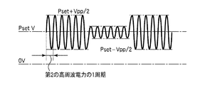
下部電極であるサセプタ16には、第2の整合器88を介して第2の高周波電源90が電気的に接続されている。この第2の高周波電源90から下部電極サセプタ16に高周波電力が供給されることにより、半導体ウエハWにバイアスが印加され半導体ウエハWにイオンが引き込まれる。第2の高周波電源90は、400kHz〜13.56MHzの範囲内の周波数、例えば2MHzの高周波電力を出力する。この第2の高周波電源90には、第2の高周波電源90を制御するRF制御器95が接続されている。このRF制御器95は、第2の高周波電源90からの高周波電力が、半導体ウエハWの被エッチング膜にデポが堆積する第1のパワーと半導体ウエハWの被エッチング膜のエッチングが進行する第2のパワーとの間で所定周期でパワー変調するようにパワー制御を行うことが可能となっており、通常の連続モードとパワー制御モードとの間で切り換え可能となっている。パワー変調の典型例としては、図3に示すようなパルス状を挙げることができるが、これに限るものではない。なお、この例ではパルスのデューティー比が50%である。また、この際の出力電圧波形は、図4のようになる。一周期中の最大電圧値と最小電圧値との差がVPPとなる。なお、図4中のPsetは設定電圧を示す。
A second high
なお、このRF制御器95は、第2の整合器88にも接続されており、第2の整合器88も制御する。また、RF制御器95は、第1の高周波電源48および第1の整合器46にも接続されており、これらも制御可能となっている。
The
第2の整合器88は第2の高周波電源90の内部(または出力)インピーダンスに負荷インピーダンスを整合させるためのもので、チャンバ10内にプラズマが生成されている時に第2の高周波電源90の内部インピーダンスとチャンバ10内のプラズマを含めた負荷インピーダンスが見かけ上一致するように機能する。この第2の整合器88は、図5に示すように、第2の高周波電源90の給電ライン96から分岐して設けられた第1の可変コンデンサ97と、給電ライン96のその分岐点の第2の高周波電源90側に設けられた第2の可変コンデンサ98と、分岐点の反対側に設けられたコイル99とを有している。本実施形態の場合、通常のプラズマエッチングと異なり、第2の高周波電源90は、高周波電力が所定周期でパワー変調されるパワー変調モードで動作するため、このパワー変調モードの際に、RF制御器95が、第2の整合器88における整合動作を前記パワー変調に同期させて切り換えるように制御する。この場合に、RF制御器95は、第2の高周波電力供給ユニット90をパワー変調モードで動作させているときに、第1のパワーの際には第2の整合器88の動作を行わないように制御し、第2のパワーの際には第2の整合器88が第2の高周波電源90の内部インピーダンスとチャンバ10内のプラズマを含めた負荷インピーダンスとが一致するような動作を行うように制御する。具体的には、相対的にパワーが大きい第2のパワーのときのみ第1の可変コンデンサ97の容量C1と第2の可変コンデンサ98の容量C2とを独立に制御し、第1のパワーのときは容量C1、容量C2をそれぞれ固定とする。この場合に、通常の整合器のように順方向のパワーPfのみの制御ではハンチングが生じるため、第2の整合器88として反射パワーPrも加味したロードパワーPL(=Pf−Pr)制御付きのものを用いる。具体的には、第1のパワーの際には、第2の高周波電源90が出力するパワー値Pfと、チャンバ10内のプラズマを含めた負荷インピーダンスによって反射されるパワー値Prとの差分である、下部電極であるサセプタ16に供給されるパワー値PLが常に一定になるように、第2の高周波電源90を制御する。第1の高周波電源46についても、第2の高周波電源からの高周波電力がパワー変調されている影響を受けるため、同様にロードパワー制御付きのものとして同様の制御を行うことが好ましい。
The
上部電極34には、第1の高周波電源48からの高周波電力(60MHz)は通さずに第2の高周波電源90からの高周波電力(2MHz)をグランドへ通すためのローパスフィルタ(LPF)92が電気的に接続されている。このローパスフィルタ(LPF)92は、好適にはLRフィルタまたはLCフィルタで構成されるが、1本の導線だけでも第1の高周波電源48からの高周波電力(60MHz)に対しては十分大きなリアクタンスを与えることができるので、それで済ますこともできる。一方、下部電極であるサセプタ16には、第1の高周波電源48からの高周波電力(60MHz)をグランドに通すためのハイパスフィルタ(HPF)94が電気的に接続されている。
The
チャンバ10の底部には排気口80が設けられ、この排気口80に排気管82を介して排気装置84が接続されている。排気装置84は、ターボ分子ポンプなどの真空ポンプを有しており、チャンバ10内を所望の真空度まで減圧可能となっている。また、チャンバ10の側壁には半導体ウエハWの搬入出口85が設けられており、この搬入出口85はゲートバルブ86により開閉可能となっている。また、チャンバ10の内壁に沿ってチャンバ10にエッチング副生物(デポ)が付着することを防止するためのデポシールド11が着脱自在に設けられている。すなわち、デポシールド11がチャンバ壁を構成している。また、デポシールド11は、内壁部材26の外周にも設けられている。チャンバ10の底部のチャンバ壁側のデポシールド11と内壁部材26側のデポシールド11との間には排気プレート83が設けられている。デポシールド11および排気プレート83としては、アルミニウム材にY2O3等のセラミックスを被覆したものを好適に用いることができる。
An
デポシールド11のチャンバ内壁を構成する部分のウエハWとほぼ同じ高さの部分には、グランドにDC的に接続された導電性部材(GNDブロック)91が設けられており、これにより後述するような異常放電防止効果を発揮する。なお、この導電性部材91は、プラズマ生成領域に設けられていれば、その位置は図1の位置に限られず、例えばサセプタ16の周囲に設ける等、サセプタ16側に設けてもよく、また上部電極34の外側にリング状に設ける等、上部電極近傍に設けてもよい。
A conductive member (GND block) 91 connected to the ground in a DC manner is provided at a portion of the
プラズマ処理装置の各構成部、例えば電源系やガス供給系、駆動系、さらにはRF制御器95等は、制御部(全体制御装置)100に接続されて制御される構成となっている。また、制御部100には、工程管理者がプラズマ処理装置を管理するためにコマンドの入力操作等を行うキーボードや、プラズマ処理装置の稼働状況を可視化して表示するディスプレイ等からなるユーザーインターフェース101が接続されている。
Each component of the plasma processing apparatus, such as a power supply system, a gas supply system, a drive system, and an
さらに、制御部100には、プラズマ処理装置で実行される各種処理を制御部100の制御にて実現するための制御プログラムや、処理条件に応じてプラズマ処理装置の各構成部に処理を実行させるためのプログラムすなわちレシピが格納された記憶部102が接続されている。レシピは記憶部102の中の記憶媒体に記憶されている。記憶媒体は、ハードディスクや半導体メモリであってもよいし、CDROM、DVD、フラッシュメモリ等の可搬性のものであってもよい。また、他の装置から、例えば専用回線を介してレシピを適宜伝送させるようにしてもよい。
Further, the
そして、必要に応じて、ユーザーインターフェース101からの指示等にて任意のレシピを記憶部102から呼び出して制御部100に実行させることで、制御部100の制御下で、プラズマ処理装置での所望の処理が行われる。なお、本発明の実施の形態で述べるプラズマ処理装置(プラズマエッチング装置)は、この制御部100を含むものとする。
Then, if necessary, an arbitrary recipe is called from the
このように構成されるプラズマ処理装置においてエッチング処理を行う際には、まず、ゲートバルブ86を開状態とし、搬入出口85を介してエッチング対象である半導体ウエハWをチャンバ10内に搬入し、サセプタ16上に載置する。そして、処理ガス供給源66からエッチングのための処理ガスを所定の流量でガス拡散室40へ供給し、ガス通流孔41およびガス吐出孔37を介してチャンバ10内へ供給しつつ、排気装置84によりチャンバ10内を排気し、その中の圧力を例えば0.1〜150Paの範囲内の設定値とする。ここで、処理ガスとしては、従来用いられている種々のものを採用することができ、例えばC4F8ガスのようなフロロカーボンガス(CxFy)に代表されるハロゲン元素を含有するガスを好適に用いることができる。さらに、ArガスやO2ガス等の他のガスが含まれていてもよい。
When performing the etching process in the plasma processing apparatus configured as described above, first, the
このようにチャンバ10内にエッチングガスを導入した状態で、第1の高周波電源48からプラズマ生成用の高周波電力を上部電極34に印加するとともに、第2の高周波電源90よりイオン引き込み用の高周波電力を下部電極であるサセプタ16に印加する。そして、可変直流電源50から所定の直流電圧を上部電極34に印加する。さらに、静電チャック18のための直流電源22から直流電圧を静電チャック18の電極20に印加して、半導体ウエハWを静電チャック18に固定する。
With the etching gas introduced into the
上部電極34の電極板36に形成されたガス吐出孔37から吐出された処理ガスは、高周波電力により生じた上部電極34と下部電極であるサセプタ16間のグロー放電中でプラズマ化し、このプラズマで生成されるラジカルやイオンによって半導体ウエハWの被処理面がエッチングされる。また、このように上部電極34にプラズマ形成用の第1の高周波電力を供給し、下部電極であるサセプタ16にイオン引き込み用の第2の高周波電力を供給するので、プラズマの制御マージンを広くすることができる。
The processing gas discharged from the
本実施形態では、このようにしてプラズマが形成される際に、上部電極34に27MHz以上の高い周波数領域の高周波電力を供給しているので、プラズマを好ましい状態で高密度化することができ、より低圧の条件下でも高密度プラズマを形成することができる。
In the present embodiment, when plasma is formed in this way, high frequency power in a high frequency region of 27 MHz or higher is supplied to the
また、このようにプラズマが形成される際に、コントローラ51により可変直流電源50から上部電極34に印加される直流電圧の極性および大きさを制御することにより、印加電極である上部電極34の表面つまり電極板36の表面に対する所定の(適度な)スパッタ効果が得られる程度にその表面の自己バイアス電圧Vdcが深くなるように、つまり上部電極34表面でのVdcの絶対値が大きくなるようにすることができる。第1の高周波電源48から印加される高周波電力のパワーが低い場合に、上部電極34にポリマーが付着するが、可変直流電源50から適切な直流電圧を印加することにより、上部電極34に付着したポリマーをスパッタして上部電極34の表面を清浄化することができ、かつ、半導体ウエハW上に最適な量のポリマーを供給することができる。これにより、フォトレジスト膜の表面荒れを解消することができ、かつ下地膜との間のエッチング選択比を高くすることができる。
Further, when the plasma is formed in this way, the
なお、上部電極34に直流電圧を印加することにより、上部電極34自体をスパッタしてフォトレジスト膜表面にカーバイドを形成してフォトレジスト膜を強化することや、自己バイアス電圧Vdcが深くなることにより、上部電極34側に形成されるプラズマシースの厚さが厚くなってプラズマが縮小化されることによる、半導体ウエハW上の実効レジデンスタイムの増加およびプラズマがウエハW上に集中することによる解離空間の減少によって、フロロカーボン系の処理ガスの解離抑制にともなうフォトレジスト膜の耐エッチング性を向上するといった効果を得ることもできる。また、上部電極34に直流電圧を印加することにより、上部電極34近傍に生成された電子が処理空間の鉛直方向へ加速され、シェーディング効果を抑制してボーイングのない良好な加工形状を得ることができるといった効果も得ることができる。なお、可変直流電源50からの印加電圧を制御する代わりに、印加電流または印加電力を制御するようにしてもよい。
By applying a DC voltage to the
このように上部電極34に直流電極を印加することにより、種々の効果が得られ、特に被処理基板である半導体ウエハWに適切にポリマーを供給する効果によって、被エッチング膜と下地のエッチングストップ膜との選択比を大きくすることが可能となるが、低誘電率バリア膜であるSiC膜を下地エッチングストップ膜として使用して上層の被エッチング膜であるSiOC系Low−k膜をエッチングする場合には、両者の組成が極めて近接しているため、このように直流電圧を印加しても十分なエッチング選択比を確保することができる条件のマージンが極めて狭い。
By applying the DC electrode to the
このことを具体的に説明する。
図6は、横軸に第2の高周波電源90から印加されるバイアス用高周波電力(13.56MHz)の自己バイアス電圧Vdcをとり、縦軸にエッチングレートをとった、SiOC系Low−k膜とSiC膜のエッチング特性を示すグラフである。このとき、処理ガスとしてはC4F8、Ar、N2を用い、これらの流量をそれぞれ10mL/min(sccm)、500mL/min(sccm)、100mL/min(sccm)とし、圧力を6Paとし、第1の高周波電源48として周波数が60MHzのものを用いてパワーを1000Wとし、第2の高周波電源90として周波数が13.56MHzのものを用いてパワーを2000Wとした。チャンバ内にプラズマを生成すると、上部電極から半導体ウエハにポリマーが供給されバイアスが印加されていないとデポが生じるが、自己バイアス電圧Vdcの絶対値を上げて行くとエッチングが進行するようになる。このとき、SiOC系Low−k膜を高精度でエッチングするためには、SiOC系Low−k膜がエッチングされ、下地のSiC膜はエッチングされないようなVdcが求められる。しかし、SiOC系Low−k膜とSiC膜とは組成が近接しているため、図に示すようにエッチング挙動が似ており、通常のエッチングでは高選択比をとるためのエッチングを行うことができるマージンは極めて狭く、エッチングレートを上げることができない。
This will be specifically described.
FIG. 6 shows a SiOC-based Low-k film in which the horizontal axis represents the self-bias voltage Vdc of the high frequency power for bias (13.56 MHz) applied from the second high
エッチングはエッチング対象膜にバイアスを印加してイオンを引き込むことにより進行するが、上述したようにエッチング対象膜にはポリマーが供給されて堆積されるため、エッチングを進行させるためにはポリマーの厚さよりもイオン侵入深さのほうが大きくなるようにVdc(ウエハに入射するイオンエネルギー)を選択することが必要である。一方、エッチング対象膜がエッチングされた後は、下地膜に堆積されるポリマーの厚さがイオン侵入深さよりも厚ければ、下地膜のエッチングがストップし、選択性の高いエッチングが実現する。しかし、図6のようにエッチング挙動が被エッチング膜と下地膜とで近接している場合には、高いエッチングレートで被エッチング膜をエッチングした後、連続的にオーバーエッチングを行うと、被エッチング膜が抜けた時点で下地膜上のポリマー厚さがイオン侵入深さよりも薄くなっており、下地膜がエッチングされてしまう。 Etching proceeds by applying a bias to the film to be etched and drawing ions, but as described above, polymer is supplied and deposited on the film to be etched. It is also necessary to select Vdc (ion energy incident on the wafer) so that the ion penetration depth becomes larger. On the other hand, after the etching target film is etched, if the thickness of the polymer deposited on the base film is larger than the ion penetration depth, the etching of the base film is stopped, and etching with high selectivity is realized. However, when the etching behavior is close to the film to be etched and the base film as shown in FIG. 6, if the film to be etched is etched at a high etching rate and then continuously overetched, At the point of time, the polymer thickness on the base film becomes thinner than the ion penetration depth, and the base film is etched.
そこで、本実施形態では、被エッチング膜が抜ける時点、すなわち被エッチング膜がエッチングされてオーバーエッチングに移行する時点におけるポリマー厚さがイオン侵入深さよりも厚くなるように、被エッチング膜にポリマーが堆積される第1のパワーと被処理基板の被エッチング膜がエッチングされる第2のパワーとの間で所定周期でパワー変調するようにする。この際には、制御部100の指令によりRF制御器95が第2の高周波電源90を通常モードからパワー変調モードに切り換える。これにより、第1のパワーでポリマーを堆積させ、第2のパワーでエッチングを進行させて、オーバーエッチング開始時にイオン侵入深さよりも厚いポリマー層が形成されるようにして、エッチングストップ膜を大きく浸食させることなくエッチングを停止させることができる。
Therefore, in this embodiment, the polymer is deposited on the film to be etched so that the polymer thickness at the time when the film to be etched comes off, that is, when the film to be etched is etched and shifts to overetching becomes thicker than the ion penetration depth. The power is modulated at a predetermined cycle between the first power to be processed and the second power to be etched on the etching target film of the substrate to be processed. At this time, the
以上のことを図面を参照して詳細に説明する。
ここでは、Cu配線層201の上にエッチングストップ膜であるSiC膜202が形成され、その上に被エッチング膜であるSiOC系Low−k膜203が形成され、フォトレジスト膜204をマスクとしてSiOC系Low−k膜203をエッチングする場合について説明する。
The above will be described in detail with reference to the drawings.
Here, an
まず、従来の連続モードの場合には、図7の(a)に示すメインエッチング末期の状態から図7の(b)に示すようなSiOC系Low−k膜203が抜けた瞬間(オーバーエッチングを始める瞬間)は、ホール底の下地のSiC膜202上に形成されているポリマー層205の厚さが薄く、SiC膜202がエッチングされ浸食されてしまう。そして、図7の(c)に示すようにSiC膜202膜がかなり浸食された時点でオーバーエッチングが飽和される(オーバーエッチング25%)。
First, in the case of the conventional continuous mode, the moment when the SiOC-based Low-
これに対して、図7の(a)に示すメインエッチング末期の状態でパワー変調モードに切り換えることにより、図7の(d)に示すオーバーエッチングの瞬間の第1のパワーの時には、ホール底のSiC膜202の上のポリマー層205の厚さが厚くなり、図7の(e)に示すように、その後第2のパワーのエッチングモードになってもイオン侵入深さがポリマー層205の厚さよりも小さくなるため、図7の(f)に示すようにエッチングストップ膜であるSiC膜202はほとんど浸食されない。
On the other hand, by switching to the power modulation mode in the final stage of main etching shown in FIG. 7A, the first power at the moment of over-etching shown in FIG. The thickness of the
図8は、横軸にバイアスパワーをとり縦軸にポリマー層厚さをとって、上記現象を模式的にまとめたグラフである。また、図8中に、ポリマー層205またはSiC膜202へのイオンの侵入深さも描いている(スケールはポリマー深さと同じ)。この図に示すように、連続モードの場合には、SiOC系Low−k膜203とSiC膜202のエッチング特性が類似している関係上、上述したように、イオンの侵入深さがSiC膜202上のポリマー層205の厚さより小さい、SiC膜202が浸食されない領域は極めて狭く、しかもバイアスパワーを小さくしてSiOC系Low−k膜203のエッチングレートを小さくせざるを得ないが、オーバーエッチング直前にバイアスパワーをパワー変調する場合には、SiC膜202が浸食されない領域を広くすることができ、しかもバイアスパワーを大きくしてSiOC系Low−k膜203のエッチングレートを高くすることができる。
FIG. 8 is a graph schematically summarizing the above phenomenon with the horizontal axis representing the bias power and the vertical axis representing the polymer layer thickness. In FIG. 8, the penetration depth of ions into the
このようなバイアスのパワー変調を用いた場合のプロセスマージンを図6の連続モードの場合と比較して図9に示す。この図に示すように、オーバーエッチング直前にパワー変調を用いることにより、プロセスマージンが広がり、Vdcが−800V付近の高エッチングレートのエッチングでも、下地のSiC膜をほとんどエッチングすることなくエッチング対象膜であるSiOC系Low−k膜をエッチング可能となることがわかる。すなわち、下地膜に対する選択比が高くかつ高エッチングレートでエッチング対象膜であるSiOC系Low−k膜をエッチングすることができる。 FIG. 9 shows a process margin when such bias power modulation is used in comparison with the continuous mode shown in FIG. As shown in this figure, by using power modulation immediately before over-etching, the process margin is widened, and even when etching at a high etching rate near Vdc of −800 V, the underlying SiC film is hardly etched and the target film is etched. It can be seen that a certain SiOC-based Low-k film can be etched. That is, it is possible to etch the SiOC-based Low-k film, which is a target film to be etched, with a high selectivity with respect to the base film and a high etching rate.
図10は、ポリマー膜厚とイオン(Arイオン)の吸収エネルギーとの関係をシミュレーションした結果をイオンの照射エネルギー毎に示したグラフである。通常のエッチングの場合、イオン照射エネルギー分布は500eV〜1keVまでの範囲が大部分であることが知られており、図10からポリマー厚さが1keVにおけるイオンエネルギー吸収範囲は5nm程度までであるから、ポリマー厚さが数nm以上、好ましくは5nm以上であればイオンの侵入深さをポリマー層の厚さよりも小さくすることができることが理解される。 FIG. 10 is a graph showing the result of simulating the relationship between the polymer film thickness and the absorption energy of ions (Ar ions) for each ion irradiation energy. In the case of normal etching, the ion irradiation energy distribution is known to be mostly in the range from 500 eV to 1 keV, and from FIG. 10, the ion energy absorption range at a polymer thickness of 1 keV is up to about 5 nm. It is understood that the ion penetration depth can be made smaller than the thickness of the polymer layer if the polymer thickness is several nm or more, preferably 5 nm or more.
本実施形態において、第2の高周波電源90からの高周波電力をパワー変調する際の波形の典型例としては上述したようにパルス状を挙げることができる。ただし、これに限るものではなく第1のパワーと第2のパワーとで変調していれば、サインカーブ等の他の波形であってもよい。
In the present embodiment, as a typical example of the waveform when the high frequency power from the second high
パワー変調の際には、パワーが低いほうの第1のパワーは0よりも大きいことが好ましい。パワーを0にするよりもある程度のパワーを保持していたほうがポリマーのデポを有効に供給することができる。第1のパワーおよび第2のパワーは、他のエッチング条件や膜の条件等によって適宜設定されるが、第1のパワーは10〜500Wの範囲が好ましく、第2のパワーは100〜5000Wの範囲が好ましい。さらには、第2のパワーは100〜1000Wの範囲がより好ましい。 At the time of power modulation, it is preferable that the lower first power is greater than zero. A polymer depot can be supplied more effectively if a certain amount of power is maintained than if the power is zero. The first power and the second power are appropriately set depending on other etching conditions, film conditions, etc., but the first power is preferably in the range of 10 to 500 W, and the second power is in the range of 100 to 5000 W. Is preferred. Furthermore, the second power is more preferably in the range of 100 to 1000W.
また、パワー変調の周波数は、0.25〜100Hzが好ましい。この範囲でポリマー層の生成が適度な範囲となる。すなわち、パワー変調(パルス)のデューティー比が50%の場合に、周波数が100Hzを超えるとポリマーのデポが生じる第1のパワーの時間が1周期で10mS未満となり、十分なデポが形成され難くなるおそれがあり、周波数が0.25Hz未満であると1周期あたりの第1のパワーの時間が2Sを超えてポリマー層が厚くなりすぎるおそれがある。 The frequency of power modulation is preferably 0.25 to 100 Hz. Within this range, the generation of the polymer layer is in an appropriate range. That is, when the duty ratio of power modulation (pulse) is 50%, if the frequency exceeds 100 Hz, the time of the first power at which polymer deposition occurs is less than 10 mS in one cycle, and it is difficult to form a sufficient deposit. If the frequency is less than 0.25 Hz, the time of the first power per cycle may exceed 2S and the polymer layer may become too thick.
パワー変調(パルス)のデューティー比(第2のパワーの時間/1周期の全体の時間)は典型例として50%を挙げることができるが、エッチングの条件や被エッチング膜および下地膜の条件等に応じて1〜99%の間で適切に調整することができる。 The duty ratio of power modulation (pulse) (second power time / total time of one cycle) can be 50% as a typical example, but it depends on the etching conditions, conditions of the film to be etched and the base film, etc. Accordingly, it can be appropriately adjusted between 1-99%.
エッチングに際しては、まず、バイアスパワーを変調しない通常のモードで高エッチングレートにて被エッチング膜をエッチングし、被エッチング膜のエッチング終了前にバイアスパワーを上述のようなパワー変調モードへ切り換えるが、この切り換えは、被エッチング膜がエッチングされて下地膜が見えた際に適切な量のポリマー層が形成されているようなタイミングで行うことが必要である。オーバーエッチングに入る直前にパワー変調モードへ切り換えたのではオーバーエッチング時にポリマー層の厚さが不十分になり、逆に、早く切り換え過ぎた場合には、エッチングレートが低下してしまう。したがって、下地膜が見えた際に適切な量のポリマー層が形成することができる時間が確保できるように、オーバーエッチングに入る時点にできるだけ近いタイミングで切り換えを行うことが好ましく、エッチング条件等にもよるが、被エッチング膜の残膜が20〜30nmの時点で切り換えることが好ましい。 In the etching, first, the film to be etched is etched at a high etching rate in a normal mode in which the bias power is not modulated, and the bias power is switched to the power modulation mode as described above before the etching of the film to be etched. The switching needs to be performed at such a timing that an appropriate amount of polymer layer is formed when the etching target film is etched and the underlying film is visible. If the mode is switched to the power modulation mode immediately before the overetching, the thickness of the polymer layer becomes insufficient at the time of overetching, and conversely, if it is switched too quickly, the etching rate is lowered. Therefore, it is preferable to perform switching at a timing as close as possible to the time of entering overetching so that an appropriate amount of polymer layer can be formed when the base film is visible, and etching conditions, etc. However, it is preferable to switch when the remaining film to be etched is 20 to 30 nm.
このようなパワー変調モードでエッチングする際には、上部電極34に可変直流電源50から直流電圧を印加することにより、上述したようなポリマー供給の効果が得られるため、ポリマー層を確保する観点から有利である。また、直流電圧を印加していない時には、バイアスパワーが変調することにより上部電極34に第1の高周波電源から印加されるプラズマ生成用の高周波電力の反射波が増大してプラズマが不安定になるおそれがある。そこで、可変直流電源50から上部電極34に直流電圧を印加することで、上部電極34側に形成されるプラズマシースの厚さが固定されるので、上部電極34に印加されるプラズマ生成用の高周波電力の反射波が減少し、プラズマを安定させることができる。よって、プロセスの安定性や第1の高周波電源48の寿命を向上させることができ、その点からも直流電圧を印加することが有利である。
When etching in such a power modulation mode, since the effect of polymer supply as described above can be obtained by applying a DC voltage from the variable
上部電極34に印加される直流電圧は、エッチング条件に応じて適宜設定されるが、通常の連続モードの場合もパワー変調モードの場合も、−300〜−2kVの範囲が好ましい。
The DC voltage applied to the
なお、第1の高周波電源48から上部電極34に印加される高周波電力の周波数、および第2の高周波電源90からサセプタ16に印加される高周波電力の周波数の好ましい範囲は、通常の連続モードの場合およびパワー変調モードの場合によらず、上述したように前者が27〜100MHzの範囲、後者が400kHz〜13.56MHzの範囲が好ましい。また、第1の高周波電源48から供給される高周波電力のパワーは、通常の連続モードの場合もパワー変調モードの場合も500〜5000Wの範囲が好ましい。さらに、通常の連続モードの場合の第2の高周波電源90からのバイアス用高周波電力のパワーは、500〜5000Wの範囲が好ましい。
The preferred range of the frequency of the high frequency power applied from the first high
次に、本実施形態の効果を確認した実験について説明する。
ここでは、下地膜であるSiC膜を30nm形成した後、その上にエッチング対象膜であるSiOC系Low−k膜を300nm形成し、その上にBARCおよびパターン化されたArFレジスト膜を形成したサンプルを用い、まずArFレジスト膜をマスクとしてBARCをエッチングした後、SiOC系Low−k膜をエッチングしてビアを形成した。
Next, an experiment for confirming the effect of the present embodiment will be described.
Here, after forming a SiC film as a base film to a thickness of 30 nm, a SiOC-based low-k film as a film to be etched is formed to a thickness of 300 nm, and a BARC and a patterned ArF resist film are formed thereon. First, the BARC was etched using the ArF resist film as a mask, and then the SiOC Low-k film was etched to form a via.
エッチングの際の条件は、以下のとおりとした。なお、オーバーエッチングについては、本実施形態に従ってパワー変調モードで印加した場合(実施例)と、従来のようにバイアスを連続モードで印加した場合(比較例)とについて行った。
(1)メインエッチング(連続モード)
チャンバ内圧力:6.65Pa(50mT)
上部印加高周波パワー(60MHz):400W
下部印加高周波パワー(400kHz):500W
処理ガスおよび流量:C4F8/Ar/N2=4/1000/500mL/min(sccm)
上部直流電圧:−900V
時間:60sec
(2)オーバーエッチング
(a)実施例
チャンバ内圧力:6.65Pa(50mT)
上部印加高周波パワー(60MHz):400W
下部印加高周波パワー(400kHz):100W/800Wで変調
パワー変調の際のパルスパラメータ
周波数:15.0Hz
デューティー比:50%
Vpp:1.4V
処理ガスおよび流量:C4F8/Ar/N2=8/1000/80mL/min(sccm)
上部直流電圧:−900V
(b)比較例
チャンバ内圧力:6.65Pa(50mT)
上部印加高周波パワー(60MHz):400W
下部印加高周波パワー(400kHz):800W
処理ガスおよび流量:C4F8/Ar/N2=4/1000/500mL/min(sccm)
上部直流電圧:−900V
(3)共通条件
温度:上部電極/ウエハ/下部電極=60/60/0℃
The conditions for etching were as follows. Note that overetching was performed according to the present embodiment when applied in a power modulation mode (Example) and when a bias was applied in a continuous mode as in the past (Comparative Example).
(1) Main etching (continuous mode)
Chamber pressure: 6.65 Pa (50 mT)
Upper applied high frequency power (60 MHz): 400 W
Lower applied high frequency power (400 kHz): 500 W
Process gas and flow rate: C 4 F 8 / Ar / N 2 = 4/1000/500 mL / min (sccm)
Upper DC voltage: -900V
Time: 60sec
(2) Over-etching (a) Example Chamber pressure: 6.65 Pa (50 mT)
Upper applied high frequency power (60 MHz): 400 W
Lower applied high frequency power (400 kHz): Modulated at 100 W / 800 W Pulse parameters for power modulation
Frequency: 15.0Hz
Duty ratio: 50%
Vpp: 1.4V
Process gas and flow rate: C 4 F 8 / Ar / N 2 = 8/1000/80 mL / min (sccm)
Upper DC voltage: -900V
(B) Comparative example Pressure in chamber: 6.65 Pa (50 mT)
Upper applied high frequency power (60 MHz): 400 W
Lower applied high frequency power (400 kHz): 800 W
Process gas and flow rate: C 4 F 8 / Ar / N 2 = 4/1000/500 mL / min (sccm)
Upper DC voltage: -900V
(3) Common conditions Temperature: upper electrode / wafer / lower electrode = 60/60/0 ° C.
これらの条件でエッチングを行った後、サンプルを1%HF水溶液に30秒浸漬させて、SiCの浸食の浸食量を把握した。なお、実施例におけるバイアスパワー印加の通常モードからパワー変調モードへの切り換えは、オーバーエッチング開始時点から30sec前とした。
After etching under these conditions, the sample was immersed in a 1% HF aqueous solution for 30 seconds, and the erosion amount of SiC erosion was grasped. In the embodiment, the bias power application was switched from the normal mode to the
結果を図11に示す。図11は、横軸にオーバーエッチングの時間をとり、縦軸にSiC膜の浸食量(nm)をとって、実施例と比較例を対比した図である。この図に示すように、比較例の場合には、オーバーエッチング開始直後に9nm程度まで大きく浸食したのに対し、実施例の場合には、初期に3nm程度浸食された後、オーバーエッチング40%までほぼ一定で飽和していることが確認された。このことから、本実施形態のバイアスのパワー変調モードの効果が確認された。 The results are shown in FIG. FIG. 11 is a diagram comparing the example and the comparative example, with the horizontal axis representing the over-etching time and the vertical axis representing the erosion amount (nm) of the SiC film. As shown in this figure, in the case of the comparative example, it was greatly eroded to about 9 nm immediately after the start of overetching, whereas in the case of the example, after about 3 nm was initially eroded, up to 40% of overetching. It was confirmed to be almost constant and saturated. From this, the effect of the power modulation mode of the bias of this embodiment was confirmed.
なお、本実施形態では、被エッチング膜としてSiOC系(有機系)のLow−k膜を例示したが、無機系のLow−k膜であっても当然よい。また、下地膜としてSiC膜を例示したが、例えば窒化シリコン膜(SiN)であってもよい。さらに、本実施形態では被エッチング膜としてSiOC系Low−k膜、下地膜としてSiC膜の組み合わせを例示したが、被エッチング膜が下地膜に対して選択比を取り難い場合の全般に適用可能である。また、上記実施形態では、バイアスを連続モードからパワー変調モードに切り換える場合について示したが、十分なエッチングレートを得ることができれば、パワー変調モードのみを採用することもできる。 In this embodiment, the SiOC-based (organic) Low-k film is exemplified as the film to be etched, but an inorganic Low-k film may naturally be used. Further, although the SiC film is exemplified as the base film, for example, a silicon nitride film (SiN) may be used. Furthermore, in this embodiment, the combination of the SiOC-based low-k film as the film to be etched and the SiC film as the base film is exemplified. is there. In the above-described embodiment, the case where the bias is switched from the continuous mode to the power modulation mode has been described. However, if a sufficient etching rate can be obtained, only the power modulation mode can be employed.
次に、本実施形態における他の適用例について説明する。
ここでは、被エッチング膜のマスクに対する選択比を高めるために、上述したパワー変調モードを利用した例について説明する。
図12はこの例に適用するための半導体ウエハの構造を示す断面図である。符号301はLow−k膜であり、その上にハードマスク層としてのTiN膜302が形成され、その上に無機犠牲膜303およびフォトレジスト膜304が形成されている。ハードマスク層としてはTiNの代わりにTi膜を用いてもよい。このような構造において、TiN膜302をマスクとしてLow−k膜301をエッチングしてホール305を形成する場合には、TiN膜302に対して大きな選択比でエッチングすることが望まれる。そのためには、Low−k膜301に対してはエッチングが進行し、TiN膜302に対してはポリマーの堆積が多くエッチングが進行し難くなるような条件のパワー変調モードとなるように第2の高周波電源90を制御しながらエッチングを行うことが有効である。
Next, another application example in the present embodiment will be described.
Here, an example in which the above-described power modulation mode is used to increase the selectivity of the film to be etched with respect to the mask will be described.
FIG. 12 is a sectional view showing the structure of a semiconductor wafer for application to this example.
次に、本実施形態のさらに他の適用例について説明する。
ここでは、マイクロローディング効果を緩和するために、上述したパワー変調モードを利用した例について説明する。
図13に示すように、下地膜401の上にエッチングストップ膜であるSiC膜402が形成され、その上に被エッチング膜であるSiOC系Low−k膜403が形成され、フォトレジスト膜404をマスクとしてSiOC系Low−k膜403に小さいサイズのビア405と例えばガードリング(GR)等の大きいエリアのトレンチ406をエッチングする場合、マイクロローディング効果により、サイズの小さいビア405にはCF系ラジカルが入りにくく、そのエッチレートが遅くなり、逆にサイズの大きいトレンチ406ではエッチング速度が速くなる傾向にある。
Next, still another application example of this embodiment will be described.
Here, an example in which the above-described power modulation mode is used to reduce the microloading effect will be described.
As shown in FIG. 13, an
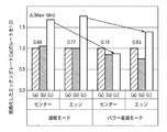
このようなマイクロローディング効果を抑制するために、上述のようなパワー変調モードでバイアスを印加しながらエッチングを行うことが有効である。このようなパワー変調モードでバイアスを印加することにより、大きいエリアのトレンチ406のエッチングレートのみを抑制してマイクロローディング効果を緩和することができる。具体的には、上述したように、パワー変調モードにおける高パワーである第2のパワーでエッチングが進行し、低パワーである第1のパワーではCF系プリカーサーが堆積してエッチングが抑制されるが、そのようなエッチングの抑制効果はエッチングエリアの大きいトレンチ406でより大きく発揮されるため、ビア405とトレンチ406のエッチングレートの差が小さくなり、マイクロローディング効果が緩和される。
In order to suppress such a microloading effect, it is effective to perform etching while applying a bias in the power modulation mode as described above. By applying a bias in such a power modulation mode, only the etching rate of the
次に、本適用例を実際に適用した結果について説明する。
ここでは、エッチング対象膜としてSiOC系Low−k膜を用い、図14に示すようなサイズの(a)楕円形ビア、(b)円形のスモールビア、(c)トレンチ(GR)をエッチングした。ここでは、下部印加高周波電力パワー変調モードにした場合と連続モードにした場合とについて比較した。その際の条件は以下の通りとした。
(1)共通条件
チャンバ内圧力:6.65Pa(50mT)
上部印加高周波パワー(60MHz):400W
上部直流電圧:−900V
温度:上部電極/ウエハ/下部電極=60/60/0℃
処理ガスおよび流量:C4F8/Ar/N2=10/1000/100mL/min(sccm)
時間:30sec
(2)パワー変調モード
下部印加高周波パワー(13.56MHz):100W/700Wで変調
パワー変調の際のパルスパラメータ
周波数:15.0Hz
デューティー比:50%
(3)連続モード
下部印加高周波パワー(13.56MHz):700Wを連続印加
Next, the result of actual application of this application example will be described.
Here, a SiOC-based Low-k film was used as an etching target film, and (a) an elliptical via, (b) a circular small via, and (c) a trench (GR) having a size as shown in FIG. 14 were etched. Here, a comparison was made between the case where the lower-applied high-frequency power modulation mode and the continuous mode were selected. The conditions at that time were as follows.
(1) Common conditions Chamber pressure: 6.65 Pa (50 mT)
Upper applied high frequency power (60 MHz): 400 W
Upper DC voltage: -900V
Temperature: Upper electrode / wafer / lower electrode = 60/60/0 ° C.
Process gas and flow rate: C 4 F 8 / Ar / N 2 = 10/1000/100 mL / min (sccm)
Time: 30sec
(2) Power modulation mode Lower applied high frequency power (13.56 MHz): modulated at 100 W / 700 W Pulse parameters for power modulation Frequency: 15.0 Hz
Duty ratio: 50%
(3) Continuous mode Lower applied high frequency power (13.56MHz): 700W continuously applied
これらエッチングを行った際のセンターおよびエッジのエッチングレートを表1にまとめて示す。また、図14(a)の楕円形ビアのエッチングレートを1.0として規格化した結果を表2に示す。さらに表2をグラフ化したものを図15に示す。 Table 1 shows the etching rates of the center and the edge when these etchings are performed. Table 2 shows the results of normalization with the etching rate of the elliptical via shown in FIG. Further, a graph of Table 2 is shown in FIG.

ところで、本実施形態において第2の高周波電源90をパワー変調モードにしたプラズマを形成する場合、より確実にプラズマを維持するために、第2の高周波電源90をプラズマ着火の際には同一パワーの連続モードで動作させ、その後パワー変調モードで動作させることが好ましい。この場合に、高周波電力および直流電圧の印加タイミングおよび印加手法も問題となる。以下、高周波電力および直流電圧の好ましい印加タイミングおよび印加手法について図16〜18を参照して説明する。
By the way, in the present embodiment, when forming the plasma in which the second high
図16の例では、第2の高周波電源90から高パワーの第2のパワーよりも低いパワーで高周波電力を連続モードで下部電極であるサセプタ16に供給開始し、所定時間経過後の時刻T1に、第1の高周波電源48から高周波電力を上部電極34に印加する。それと同時に可変直流電源50から上部電極34に直流電圧を印加する。この状態でプラズマが着火し、プラズマが安定した時点の時刻T2において第2の高周波電源90をパワー変調モードにする。これにより、プラズマが安定した後にパワー変調モードにすることになるので、パワー変調モードにおける第1のパワーのような低いパワーを供給する場合であっても、確実にプラズマを維持することができる。なお、これらの制御はRF制御器95により行われる。以下の図17および図18の例でも同様である。
In the example of FIG. 16, high-frequency power is started to be supplied from the second high-
図17の例では、第2の高周波電源90のパワーを高パワーの第2のパワーの値までスローアップし、その後パワー変調モードにしている。また、可変直流電源50の直流電圧をスローアップしている。このようにスローアップすることにより、ウエハや電源へのダメージを軽減することができる。なお、これらいずれかをスローアップするようにしてもよい。
In the example of FIG. 17, the power of the second high-
図18の例では、まず、第2の高周波電源90から高パワーの第2のパワーよりも低いパワーで高周波電力を連続モードで下部電極であるサセプタ16に供給開始し、所定時間経過後の時刻T1′に、第1の高周波電源48から設定値よりも低い高周波電力を上部電極34に印加する。それと同時に可変直流電源50から上部電極34に直流電圧を印加する。この状態でプラズマが着火し、プラズマが安定した時点の時刻T2′において第1の高周波電源48を設定値まで上昇させ、第2の高周波電源90のパワーを所定値(例えば第2のパワーの値)まで上昇させる。この場合に、第2の高周波電源90のパワーは図示するようにスローアップとすることが好ましい。そして、時刻T2′以降の所定のタイミングで第2の高周波電源90をパワー変調モードにする。これによっても、プラズマが安定した後にパワー変調モードにすることになるので、パワー変調モードにおける第1のパワーのような低いパワーを供給する場合であっても、確実にプラズマを維持することができる。なお、この例においても可変直流電源50の直流電圧をスローアップしてもよい。
In the example of FIG. 18, first, high-frequency power is started to be supplied from the second high-
次に、第2の高周波電源90とともに第1の高周波電源48もパワー変調モードにした例について説明する。
プラズマの安定性等の観点から、第2の高周波電源90をパワー変調モードとした時に、それに対応して第1の高周波電源48をもパワー変調モードにすることが好ましい場合も考えられる。この際には、RF制御器95により第2の高周波電源90のみならず第1の高周波電源48をもパワー変調するように制御する。具体的には、第1の高周波電源48を第2の高周波電源90のパワー変調モードに同期させて、第3のパワーと第4のパワーとの間でパワー変調するように制御する。この場合に、例えば図19の(a)に示すように、第1の高周波電源48と第2の高周波電源90とで、高パワーと低パワーとを同じタイミングとなるようにしてもよいし、図19の(b)に示すように、第1の高周波電源48と第2の高周波電源90とで、高パワーと低パワーとを逆のタイミングにしてもよい。
Next, an example in which the first high
From the viewpoint of plasma stability and the like, when the second high
次に、本発明の第2の実施形態について説明する。
図20は、本発明の第2の実施形態に係るプラズマエッチング装置を示す概略断面図である。
Next, a second embodiment of the present invention will be described.
FIG. 20 is a schematic cross-sectional view showing a plasma etching apparatus according to the second embodiment of the present invention.
このプラズマエッチング装置は、プラズマ生成用の高周波電力が下部電極であるサセプタに印加されるようになっている点が上記第1の実施形態に係るプラズマエッチング装置とは異なっているが、他の構成については基本的に第1の実施形態に係るプラズマエッチング装置と同様であるから、図20において、図1と同じものには同じ符号を付して説明を省略する。 This plasma etching apparatus is different from the plasma etching apparatus according to the first embodiment in that high-frequency power for plasma generation is applied to the susceptor that is the lower electrode, but other configurations are different. Since this is basically the same as the plasma etching apparatus according to the first embodiment, in FIG. 20, the same components as those in FIG.
本実施形態においては、下部電極であるサセプタ16にプラズマを生成するための第1の高周波電源48′およびバイアスを印加してイオンを引き込むための第2の高周波電源90の両方が接続されている。第1の高周波電源48′は第1の整合器89を介してサセプタ16に接続されており、第1の整合器89は第2の整合器88と同様の構成を有し、チャンバ10内にプラズマが生成されている時に第1の高周波電源48′の出力インピーダンスと負荷インピーダンスが見かけ上一致するように機能する。第1の高周波電源48′は、第1の実施形態の第1の高周波電源48と同様の機能を有しており、その周波数は27〜100MHzの範囲が好ましい。
In the present embodiment, both the first high-frequency power supply 48 'for generating plasma and the second high-
一方、上部電極34に高周波電源が接続されておらず、可変直流電源50は、ローパスフィルタ(LPF)46aを介して上部電極34に接続されている。ローパスフィルタ(LPF)46aは第1および第2の高周波電源からの高周波をトラップするものであり、好適にはLRフィルタまたはLCフィルタで構成される。
On the other hand, a high frequency power source is not connected to the
本実施形態では、下部電極にプラズマ形成用の第1の高周波(RF)電力およびイオン引き込み用の第2の高周波(RF)電力を印加する下部RF二周波印加型のプラズマエッチング装置を示しているが、その他の容量結合型プラズマエッチング装置に対する優位点として、以下の点を挙げることができる。 This embodiment shows a lower RF dual frequency application type plasma etching apparatus that applies a first high frequency (RF) power for plasma formation and a second high frequency (RF) power for ion attraction to the lower electrode. However, the following points can be cited as advantages over other capacitively coupled plasma etching apparatuses.
まず、本実施形態のように下部電極にプラズマ形成用の高周波電力を印加することで、ウエハにより近いところでプラズマを形成することができ、またプラズマが広い領域に拡散せず処理ガスの解離を抑えることができるので、処理容器内の圧力が高くプラズマ密度が低いような条件であっても、ウエハに対するエッチングレートを上昇させることができる。また、プラズマ形成用の高周波電力の周波数が高い場合でも、比較的大きなイオンエネルギーを確保することができるので高効率である。これに対して、第1の実施形態のように上部電極にプラズマ形成用の高周波電力を印加する場合には、上部電極近傍にプラズマが生成されるので、処理容器内の圧力が高くプラズマ密度が低いような条件では、ウエハに対するエッチングレートを上昇させることが比較的困難である。 First, by applying high-frequency power for plasma formation to the lower electrode as in the present embodiment, plasma can be formed at a location closer to the wafer, and plasma is not diffused over a wide area and the dissociation of the processing gas is suppressed. Therefore, the etching rate for the wafer can be increased even under conditions where the pressure in the processing chamber is high and the plasma density is low. In addition, even when the frequency of the high-frequency power for plasma formation is high, a relatively large ion energy can be secured, which is highly efficient. In contrast, when high-frequency power for plasma formation is applied to the upper electrode as in the first embodiment, plasma is generated in the vicinity of the upper electrode, so that the pressure in the processing vessel is high and the plasma density is high. Under such conditions, it is relatively difficult to increase the etching rate for the wafer.
また、本実施形態のように下部電極にプラズマ形成用の高周波電力とイオン引き込み用の高周波電力を別々に印加することで、下部電極に一周波の高周波電力を印加するタイプの装置とは異なり、プラズマエッチングに必要なプラズマ形成の機能とイオン引き込みの機能とを独立に制御することが可能となる。したがって、高い微細加工性が要求されるエッチングの条件を満たすことが可能となる。 Further, unlike the present embodiment, by separately applying the high frequency power for plasma formation and the high frequency power for ion attraction to the lower electrode as in the present embodiment, a device that applies high frequency power of one frequency to the lower electrode, It is possible to independently control the function of plasma formation and the function of ion attraction necessary for plasma etching. Therefore, it is possible to satisfy the etching conditions that require high fine workability.
本実施形態では、このような機能を有する二周波印加型のプラズマエッチング装置を基本とし、上部電極へ直流電圧を印加することによって、上述したような機能を発揮するので、近年のエッチング微細加工に適合したより高性能のエッチングが可能となるとともに、第1の実施形態と同様にバイアス用の高周波のパワー変調を行うことにより、例えばSiOC系Low−k膜とSiC膜との組み合わせのように被エッチング膜と下地膜とで組成が近接している場合であっても、被エッチング膜を高選択比および高エッチングレートでエッチングすることができる。 The present embodiment is based on a dual frequency application type plasma etching apparatus having such a function, and exhibits the above-described functions by applying a DC voltage to the upper electrode. In addition to being able to perform higher-performance etching that conforms to the first embodiment, high-frequency power modulation for bias is performed in the same manner as in the first embodiment. Even when the composition of the etching film and that of the base film are close to each other, the film to be etched can be etched with a high selectivity and a high etching rate.
なお、本実施形態においても、第1の実施形態と同様、SiC膜を下地膜としてSiOC膜をエッチングする場合等、被エッチング膜と下地膜との選択比を高めたい場合や、TiN膜をマスクとしてLow−k膜をエッチングする場合等、マスクに対して選択性の高いエッチングを行いたい場合に適用可能であるし、マイクロローディング効果を緩和したい場合にも適用可能である。また、図16で示したようなプラズマ着火シーケンスも適用可能であるし、第1の高周波電源48′をパワー変調モードで動作させることも可能である。なお、本実施形態では、被エッチング膜としてSiOC系(有機系)のLow−k膜を例示したが、無機系のLow−k膜であっても当然よい。また、下地膜としてSiC膜を例示したが、例えば窒化シリコン膜(SiN)であってもよい。さらに、本実施形態では被エッチング膜としてSiOC系Low−k膜、下地膜としてSiC膜の組み合わせを例示したが、被エッチング膜が下地膜に対して選択比を取り難い場合の全般に適用可能である。
In the present embodiment, as in the first embodiment, when the SiOC film is etched using the SiC film as a base film, the selectivity between the film to be etched and the base film is increased, or the TiN film is used as a mask. It can be applied when etching with high selectivity to the mask is desired, such as when etching a low-k film, and also when mitigating the microloading effect. Further, a plasma ignition sequence as shown in FIG. 16 can be applied, and the first high
なお、上記いずれの実施形態においても、上記第1の高周波電力および第2の高周波電力の採り得る周波数を例示すると、第1の高周波電力としては、27MHz、40MHz、60MHz、80MHz、100MHzを挙げることができ、第2の高周波電力としては、400kHz、800kHz、1MHz、2MHz、3.2MHz、12.88MHz、13.56MHzを挙げることができ、プロセスに応じて適宜の組み合わせで用いることができる。 In any of the above embodiments, when the frequencies that can be taken by the first high-frequency power and the second high-frequency power are exemplified, the first high-frequency power includes 27 MHz, 40 MHz, 60 MHz, 80 MHz, and 100 MHz. Examples of the second high frequency power include 400 kHz, 800 kHz, 1 MHz, 2 MHz, 3.2 MHz, 12.88 MHz, and 13.56 MHz, which can be used in an appropriate combination depending on the process.
以上、本発明の実施形態について説明したが、本発明は上記実施形態に限定されることなく種々変形可能である。例えば、上記実施形態では、上部電極に直流電圧を印加する例について示したが、直流電圧の印加は必須ではない。 As mentioned above, although embodiment of this invention was described, this invention can be variously deformed, without being limited to the said embodiment. For example, in the above embodiment, an example in which a DC voltage is applied to the upper electrode has been described, but application of a DC voltage is not essential.
10…チャンバ(処理容器)
16…サセプタ(下部電極)
34…上部電極
44…給電棒
46、89…第1の整合器
48…第1の高周波電源
50…可変直流電源
66…処理ガス供給源
84…排気装置
88…第2の整合器
90…第2の高周波電源
95…RF制御器
100…制御部
102…記憶部
W…半導体ウエハ(被処理基板)
10 ... Chamber (processing container)
16 ... susceptor (lower electrode)
34 ...
Claims (11)
真空排気可能な処理容器と、
処理容器内に配置された第1電極と、
前記第1電極に対向して設けられた被処理基板を支持する第2電極と、
前記第1電極または第2電極にプラズマ形成用の第1の高周波電力を供給する第1の高周波電力供給ユニットと、
前記第2電極にイオン引き込み用の第2の高周波電力を供給する第2の高周波電力供給ユニットと、
前記処理容器内に処理ガスを供給する処理ガス供給ユニットと、
前記第2の高周波電力供給ユニットを制御する制御器と
を具備し、
前記制御器は、前記第2の高周波電力供給ユニットを、前記エッチングの際には、同一パワーで連続的に高周波電力を供給する連続モードで動作させ、前記オーバーエッチングに入る前に、被処理基板の所定の膜にポリマーが堆積される第1のパワーと被処理基板の所定の膜のエッチングが進行する第2のパワーとの間で所定周期でパワー変調するパワー変調モードに切り換えるように制御することを特徴とするプラズマエッチング装置。 A plasma etching apparatus using a substrate having a structure in which an etching target film is formed on a base film as a substrate to be processed, etching the etching target film, and then over-etching.
A processing container capable of being evacuated;
A first electrode disposed in the processing vessel;
A second electrode for supporting a substrate to be processed provided to face the first electrode;
A first high-frequency power supply unit that supplies a first high-frequency power for plasma formation to the first electrode or the second electrode;
A second high-frequency power supply unit for supplying a second high-frequency power for ion attraction to the second electrode;
A processing gas supply unit for supplying a processing gas into the processing container;
A controller for controlling the second high-frequency power supply unit;
The controller operates the second high-frequency power supply unit in a continuous mode for continuously supplying high-frequency power with the same power during the etching, and before the overetching starts, the substrate to be processed Control is performed so as to switch to a power modulation mode in which power modulation is performed at a predetermined cycle between a first power at which a polymer is deposited on the predetermined film and a second power at which etching of the predetermined film on the substrate to be processed proceeds. A plasma etching apparatus characterized by that.
処理容器内に配置された第1電極と、
前記第1電極に対向して設けられた被処理基板を支持する第2電極と、
前記第1電極または第2電極にプラズマ形成用の第1の高周波電力を供給する第1の高周波電力供給ユニットと、
前記第2電極にイオン引き込み用の第2の高周波電力を供給する第2の高周波電力供給ユニットと、
前記処理容器内に処理ガスを供給する処理ガス供給ユニットとを具備するプラズマエッチング装置を用い、被処理基板として下地膜上に被エッチング膜が形成された構造のものを用い、前記第1電極および前記第2電極の間に処理ガスのプラズマを生成して被処理基板の被エッチング膜をエッチングし、その後オーバーエッチングするプラズマエッチング方法であって、
前記第2の高周波電力供給ユニットを、前記エッチングの際には、同一パワーで連続的に高周波電力を供給する連続モードで動作させ、前記オーバーエッチングに入る前に、被処理基板の所定の膜にポリマーが堆積される第1のパワーと被処理基板の所定の膜のエッチングが進行する第2のパワーとの間で所定周期でパワー変調するパワー変調モードに切り換えるようにすることを特徴とするプラズマエッチング方法。 A processing container capable of being evacuated;
A first electrode disposed in the processing vessel;
A second electrode for supporting a substrate to be processed provided to face the first electrode;
A first high-frequency power supply unit that supplies a first high-frequency power for plasma formation to the first electrode or the second electrode;
A second high-frequency power supply unit for supplying a second high-frequency power for ion attraction to the second electrode;
Using a plasma etching apparatus having a processing gas supply unit for supplying a processing gas into the processing container, and having a structure in which an etching target film is formed on a base film as a processing target substrate, the first electrode and A plasma etching method of generating plasma of a processing gas between the second electrodes to etch an etching target film of a substrate to be processed, and then over-etching ;
During the etching, the second high-frequency power supply unit is operated in a continuous mode in which high-frequency power is continuously supplied with the same power, and before entering the over-etching, a predetermined film on the substrate to be processed is applied. Switching to a power modulation mode in which power modulation is performed at a predetermined period between a first power for depositing a polymer and a second power at which etching of a predetermined film of a substrate to be processed proceeds. Etching method.
前記制御プログラムは、実行時に、請求項6から請求項10のいずれか1項に記載のプラズマエッチング方法が行われるように、コンピュータに前記プラズマエッチング装置を制御させることを特徴とするコンピュータ読取可能な記憶媒体。 A processing container capable of being evacuated, a first electrode disposed in the processing container, a second electrode for supporting a substrate to be processed provided to face the first electrode, and the first electrode or the second electrode A first high-frequency power supply unit for supplying high-frequency power for plasma formation to the second electrode, a second high-frequency power supply unit for supplying high-frequency power for ion attraction to the second electrode, and a processing gas in the processing container. A computer-readable storage medium storing a control program that operates on a computer for controlling a plasma etching apparatus including a processing gas supply unit for supplying the processing gas supply unit,
11. The computer-readable program that, when executed, causes a computer to control the plasma etching apparatus so that the plasma etching method according to any one of claims 6 to 10 is performed. Storage medium.
Priority Applications (11)
| Application Number | Priority Date | Filing Date | Title |
|---|---|---|---|
| JP2007254058A JP5192209B2 (en) | 2006-10-06 | 2007-09-28 | Plasma etching apparatus, plasma etching method, and computer-readable storage medium |
| US11/867,371 US8852385B2 (en) | 2006-10-06 | 2007-10-04 | Plasma etching apparatus and method |
| CN2007800369156A CN101523569B (en) | 2006-10-06 | 2007-10-05 | Plasma etching device and plasma etching method |
| EP17160784.9A EP3200220B1 (en) | 2006-10-06 | 2007-10-05 | Plasma etching apparatus and plasma etching method |
| PCT/JP2007/069563 WO2008044633A1 (en) | 2006-10-06 | 2007-10-05 | Plasma etching device and plasma etching method |
| KR1020097006959A KR101154559B1 (en) | 2006-10-06 | 2007-10-05 | Plasma etching device and plasma etching method |
| EP07829301.6A EP2068353B1 (en) | 2006-10-06 | 2007-10-05 | Plasma etching device and plasma etching method |
| EP19208518.1A EP3654367A1 (en) | 2006-10-06 | 2007-10-05 | Plasma etching apparatus |
| TW096137552A TWI509684B (en) | 2006-10-06 | 2007-10-05 | A plasma etch device, a plasma etch method, and a computer readable memory medium |
| US14/489,125 US10229815B2 (en) | 2006-10-06 | 2014-09-17 | Plasma etching apparatus and method |
| US16/228,960 US10861678B2 (en) | 2006-10-06 | 2018-12-21 | Plasma etching apparatus and method |
Applications Claiming Priority (5)
| Application Number | Priority Date | Filing Date | Title |
|---|---|---|---|
| JP2006275722 | 2006-10-06 | ||
| JP2006275722 | 2006-10-06 | ||
| JP2007164637 | 2007-06-22 | ||
| JP2007164637 | 2007-06-22 | ||
| JP2007254058A JP5192209B2 (en) | 2006-10-06 | 2007-09-28 | Plasma etching apparatus, plasma etching method, and computer-readable storage medium |
Related Child Applications (1)
| Application Number | Title | Priority Date | Filing Date |
|---|---|---|---|
| JP2013016925A Division JP5491648B2 (en) | 2006-10-06 | 2013-01-31 | Plasma etching apparatus and plasma etching method |
Publications (3)
| Publication Number | Publication Date |
|---|---|
| JP2009033080A JP2009033080A (en) | 2009-02-12 |
| JP2009033080A5 JP2009033080A5 (en) | 2010-11-11 |
| JP5192209B2 true JP5192209B2 (en) | 2013-05-08 |
Family
ID=39282829
Family Applications (1)
| Application Number | Title | Priority Date | Filing Date |
|---|---|---|---|
| JP2007254058A Active JP5192209B2 (en) | 2006-10-06 | 2007-09-28 | Plasma etching apparatus, plasma etching method, and computer-readable storage medium |
Country Status (7)
| Country | Link |
|---|---|
| US (3) | US8852385B2 (en) |
| EP (3) | EP2068353B1 (en) |
| JP (1) | JP5192209B2 (en) |
| KR (1) | KR101154559B1 (en) |
| CN (1) | CN101523569B (en) |
| TW (1) | TWI509684B (en) |
| WO (1) | WO2008044633A1 (en) |
Families Citing this family (72)
| Publication number | Priority date | Publication date | Assignee | Title |
|---|---|---|---|---|
| KR100801711B1 (en) * | 2007-02-27 | 2008-02-11 | 삼성전자주식회사 | Semiconductor fabrication equipments performing semiconductor etching and deposition processes and methods of forming semiconductor device using the same |
| JP5390846B2 (en) * | 2008-12-09 | 2014-01-15 | 東京エレクトロン株式会社 | Plasma etching apparatus and plasma cleaning method |
| JP2010161156A (en) * | 2009-01-07 | 2010-07-22 | Tokyo Electron Ltd | Plasma etching method |
| JP5466480B2 (en) * | 2009-02-20 | 2014-04-09 | 東京エレクトロン株式会社 | Plasma etching method, plasma etching apparatus and storage medium |
| JP2010205967A (en) * | 2009-03-04 | 2010-09-16 | Tokyo Electron Ltd | Plasma etching method, plasma etching device, and computer storage medium |
| JP5395491B2 (en) * | 2009-03-31 | 2014-01-22 | 東京エレクトロン株式会社 | Substrate processing apparatus and substrate processing method |
| JP2010238881A (en) * | 2009-03-31 | 2010-10-21 | Tokyo Electron Ltd | Plasma processing apparatus and plasma processing method |
| US8404598B2 (en) * | 2009-08-07 | 2013-03-26 | Applied Materials, Inc. | Synchronized radio frequency pulsing for plasma etching |
| KR101286242B1 (en) * | 2009-12-14 | 2013-07-15 | 삼성전자주식회사 | Semiconductor device fabricating method |
| US9373521B2 (en) | 2010-02-24 | 2016-06-21 | Tokyo Electron Limited | Etching processing method |
| JP5662079B2 (en) * | 2010-02-24 | 2015-01-28 | 東京エレクトロン株式会社 | Etching method |
| JP5709505B2 (en) * | 2010-12-15 | 2015-04-30 | 東京エレクトロン株式会社 | Plasma processing apparatus, plasma processing method, and storage medium |
| DE102011004581A1 (en) | 2011-02-23 | 2012-08-23 | Globalfoundries Dresden Module One Limited Liability Company & Co. Kg | A technique for reducing plasma-induced etch damage during the fabrication of vias in inter-layer dielectrics by modified RF power ramp-up |
| US20120302065A1 (en) * | 2011-05-26 | 2012-11-29 | Nanya Technology Corporation | Pulse-plasma etching method and pulse-plasma etching apparatus |
| KR101851005B1 (en) | 2011-06-02 | 2018-04-20 | 에스케이하이닉스 주식회사 | Method of plasma doping using plasma doping apparatus |
| CN102281698A (en) * | 2011-07-19 | 2011-12-14 | 大连理工大学 | Method for improving plasma characteristics by using impulse modulation |
| TWI450308B (en) * | 2011-07-27 | 2014-08-21 | Hitachi High Tech Corp | Plasma processing method |
| US8735291B2 (en) | 2011-08-25 | 2014-05-27 | Tokyo Electron Limited | Method for etching high-k dielectric using pulsed bias power |
| CN103035466B (en) * | 2011-10-08 | 2016-06-08 | 北京北方微电子基地设备工艺研究中心有限责任公司 | A kind of pre-cleaning method and plasma apparatus |
| US9666414B2 (en) * | 2011-10-27 | 2017-05-30 | Applied Materials, Inc. | Process chamber for etching low k and other dielectric films |
| JP5977509B2 (en) | 2011-12-09 | 2016-08-24 | 東京エレクトロン株式会社 | Plasma processing method and plasma processing apparatus |
| JP5867701B2 (en) | 2011-12-15 | 2016-02-24 | 東京エレクトロン株式会社 | Plasma processing equipment |
| JP5808012B2 (en) | 2011-12-27 | 2015-11-10 | 東京エレクトロン株式会社 | Plasma processing equipment |
| CN104106127B (en) * | 2012-02-09 | 2016-08-17 | 东京毅力科创株式会社 | The manufacture method of semiconductor-fabricating device and semiconductor-fabricating device |
| US8853070B2 (en) * | 2012-04-13 | 2014-10-07 | Oti Lumionics Inc. | Functionalization of a substrate |
| US9698386B2 (en) | 2012-04-13 | 2017-07-04 | Oti Lumionics Inc. | Functionalization of a substrate |
| JP6002556B2 (en) * | 2012-11-27 | 2016-10-05 | 株式会社日立ハイテクノロジーズ | Plasma processing apparatus and plasma processing method |
| CN103887146B (en) * | 2012-12-19 | 2016-08-31 | 中微半导体设备(上海)有限公司 | Utilize the high aspect ratio microstructures lithographic method of switchable power generator |
| US8668835B1 (en) | 2013-01-23 | 2014-03-11 | Lam Research Corporation | Method of etching self-aligned vias and trenches in a multi-layer film stack |
| JP6267989B2 (en) * | 2013-02-18 | 2018-01-24 | 東京エレクトロン株式会社 | Plasma processing method and capacitively coupled plasma processing apparatus |
| US20140262031A1 (en) * | 2013-03-12 | 2014-09-18 | Sergey G. BELOSTOTSKIY | Multi-mode etch chamber source assembly |
| JP6037914B2 (en) * | 2013-03-29 | 2016-12-07 | 富士フイルム株式会社 | Method for etching protective film and method for producing template |
| US8906810B2 (en) | 2013-05-07 | 2014-12-09 | Lam Research Corporation | Pulsed dielectric etch process for in-situ metal hard mask shape control to enable void-free metallization |
| JP6180799B2 (en) * | 2013-06-06 | 2017-08-16 | 株式会社日立ハイテクノロジーズ | Plasma processing equipment |
| US9401263B2 (en) * | 2013-09-19 | 2016-07-26 | Globalfoundries Inc. | Feature etching using varying supply of power pulses |
| JP5701958B2 (en) * | 2013-10-15 | 2015-04-15 | 東京エレクトロン株式会社 | Substrate processing equipment |
| DE102014209469A1 (en) * | 2014-05-19 | 2015-11-19 | TRUMPF Hüttinger GmbH + Co. KG | Control arrangement, control system and high-frequency power generation device |
| JP6327970B2 (en) * | 2014-06-19 | 2018-05-23 | 東京エレクトロン株式会社 | Method for etching an insulating film |
| US20160020119A1 (en) * | 2014-07-16 | 2016-01-21 | Macronix International Co., Ltd. | Method of Controlling Recess Depth and Bottom ECD in Over-Etching |
| JP6315809B2 (en) * | 2014-08-28 | 2018-04-25 | 東京エレクトロン株式会社 | Etching method |
| JP6316735B2 (en) * | 2014-12-04 | 2018-04-25 | 東京エレクトロン株式会社 | Plasma etching method |
| JP6410592B2 (en) * | 2014-12-18 | 2018-10-24 | 東京エレクトロン株式会社 | Plasma etching method |
| JP6558901B2 (en) * | 2015-01-06 | 2019-08-14 | 東京エレクトロン株式会社 | Plasma processing method |
| US9779919B2 (en) * | 2015-01-09 | 2017-10-03 | Hitachi High-Technologies Corporation | Plasma processing apparatus and plasma processing method |
| US10153139B2 (en) * | 2015-06-17 | 2018-12-11 | Applied Materials, Inc. | Multiple electrode substrate support assembly and phase control system |
| JP6552346B2 (en) * | 2015-09-04 | 2019-07-31 | 東京エレクトロン株式会社 | Substrate processing equipment |
| US9978606B2 (en) * | 2015-10-02 | 2018-05-22 | Applied Materials, Inc. | Methods for atomic level resolution and plasma processing control |
| JP6498152B2 (en) * | 2015-12-18 | 2019-04-10 | 東京エレクトロン株式会社 | Etching method |
| US10340123B2 (en) * | 2016-05-26 | 2019-07-02 | Tokyo Electron Limited | Multi-frequency power modulation for etching high aspect ratio features |
| JP6770868B2 (en) * | 2016-10-26 | 2020-10-21 | 東京エレクトロン株式会社 | Method for impedance matching of plasma processing equipment |
| US10818502B2 (en) * | 2016-11-21 | 2020-10-27 | Tokyo Electron Limited | System and method of plasma discharge ignition to reduce surface particles |
| JP7017306B2 (en) * | 2016-11-29 | 2022-02-08 | 株式会社日立ハイテク | Vacuum processing equipment |
| US10847368B2 (en) * | 2017-04-07 | 2020-11-24 | Applied Materials, Inc. | EUV resist patterning using pulsed plasma |
| JP6688763B2 (en) * | 2017-05-30 | 2020-04-28 | 東京エレクトロン株式会社 | Plasma processing method |
| JP6878154B2 (en) * | 2017-06-05 | 2021-05-26 | 東京エレクトロン株式会社 | Etching method and etching equipment |
| KR102435263B1 (en) * | 2017-07-25 | 2022-08-23 | 삼성전자주식회사 | Plasma processing apparatus and method, and method of manufacturing semiconductor device using the same |
| KR20190014623A (en) * | 2017-08-03 | 2019-02-13 | 삼성전자주식회사 | Plasma processing apparatus and method of manufacturing a semiconductor device using the same |
| KR102550393B1 (en) | 2017-10-25 | 2023-06-30 | 삼성전자주식회사 | Plasma processing apparatus and method of fabricating semiconductor device using the same |
| JP6886940B2 (en) * | 2018-04-23 | 2021-06-16 | 東京エレクトロン株式会社 | Plasma processing method |
| JP6846387B2 (en) * | 2018-06-22 | 2021-03-24 | 東京エレクトロン株式会社 | Plasma processing method and plasma processing equipment |
| JP7306886B2 (en) * | 2018-07-30 | 2023-07-11 | 東京エレクトロン株式会社 | Control method and plasma processing apparatus |
| CN110858530B (en) * | 2018-08-24 | 2023-04-14 | 北京北方华创微电子装备有限公司 | Matching network, impedance matching device, and impedance matching method |
| JP7345382B2 (en) * | 2018-12-28 | 2023-09-15 | 東京エレクトロン株式会社 | Plasma processing equipment and control method |
| JP7061981B2 (en) * | 2019-03-28 | 2022-05-02 | 東京エレクトロン株式会社 | Plasma etching equipment and plasma etching method |
| CN114342037B (en) * | 2019-08-01 | 2023-12-08 | 朗姆研究公司 | System and method for cleaning edge ring recesses |
| US11545341B2 (en) | 2019-10-02 | 2023-01-03 | Samsung Electronics Co., Ltd. | Plasma etching method and semiconductor device fabrication method including the same |
| JP7433271B2 (en) * | 2020-04-27 | 2024-02-19 | 東京エレクトロン株式会社 | Substrate processing equipment and control method for the substrate processing equipment |
| JP7201805B2 (en) * | 2020-08-27 | 2023-01-10 | 株式会社日立ハイテク | Plasma processing equipment |
| CN116803213A (en) * | 2021-02-04 | 2023-09-22 | 东京毅力科创株式会社 | Plasma processing apparatus and plasma processing method |
| CN116940705B (en) * | 2021-07-16 | 2024-03-08 | 株式会社爱发科 | Film forming method and film forming apparatus |
| CN114063479B (en) * | 2021-11-12 | 2024-01-23 | 华科电子股份有限公司 | Radio frequency power supply control method and system applied to multi-output module of etching machine |
| WO2023210399A1 (en) * | 2022-04-25 | 2023-11-02 | 東京エレクトロン株式会社 | Plasma treatment device, power source system, and plasma treatment method |
Family Cites Families (40)
| Publication number | Priority date | Publication date | Assignee | Title |
|---|---|---|---|---|
| US4263088A (en) * | 1979-06-25 | 1981-04-21 | Motorola, Inc. | Method for process control of a plasma reaction |
| KR900007687B1 (en) * | 1986-10-17 | 1990-10-18 | 가부시기가이샤 히다찌세이사꾸쇼 | Method and device for plasma processing |
| JP2728010B2 (en) | 1995-03-15 | 1998-03-18 | 株式会社日立製作所 | Plasma processing method |
| JP3122618B2 (en) * | 1996-08-23 | 2001-01-09 | 東京エレクトロン株式会社 | Plasma processing equipment |
| JP3629705B2 (en) | 1997-06-06 | 2005-03-16 | 東京エレクトロン株式会社 | Plasma processing equipment |
| JPH113879A (en) | 1997-06-11 | 1999-01-06 | Hitachi Ltd | Surface processor and its driving method |
| US6200651B1 (en) * | 1997-06-30 | 2001-03-13 | Lam Research Corporation | Method of chemical vapor deposition in a vacuum plasma processor responsive to a pulsed microwave source |
| US6093332A (en) * | 1998-02-04 | 2000-07-25 | Lam Research Corporation | Methods for reducing mask erosion during plasma etching |
| JPH11340213A (en) | 1998-03-12 | 1999-12-10 | Hitachi Ltd | Surface treatment method for sample |
| JP2000012524A (en) | 1998-06-24 | 2000-01-14 | Hitachi Ltd | Dry etching |
| KR100514150B1 (en) * | 1998-11-04 | 2005-09-13 | 서페이스 테크놀로지 시스템스 피엘씨 | A method and apparatus for etching a substrate |
| JP4230029B2 (en) | 1998-12-02 | 2009-02-25 | 東京エレクトロン株式会社 | Plasma processing apparatus and etching method |
| JP4680333B2 (en) * | 1998-12-28 | 2011-05-11 | 東京エレクトロンAt株式会社 | Plasma processing method, etching method, plasma processing apparatus and etching apparatus |
| KR100317915B1 (en) | 1999-03-22 | 2001-12-22 | 윤종용 | Apparatus for plasma etching |
| JP4831853B2 (en) * | 1999-05-11 | 2011-12-07 | 東京エレクトロン株式会社 | Capacitively coupled parallel plate plasma etching apparatus and plasma etching method using the same |
| KR100327346B1 (en) * | 1999-07-20 | 2002-03-06 | 윤종용 | Plasma etching method using selective polymer deposition and method for forming contact hole using the plasma etching method |
| JP4578651B2 (en) | 1999-09-13 | 2010-11-10 | 東京エレクトロン株式会社 | Plasma processing method, plasma processing apparatus, and plasma etching method |
| JP2002110647A (en) | 2000-09-29 | 2002-04-12 | Hitachi Ltd | Manufacturing method of semiconductor integrated circuit device |
| JP2002270586A (en) | 2001-03-08 | 2002-09-20 | Tokyo Electron Ltd | Etching method of organic based insulating film and dual damascene process |
| US7199328B2 (en) * | 2001-08-29 | 2007-04-03 | Tokyo Electron Limited | Apparatus and method for plasma processing |
| DE10309711A1 (en) * | 2001-09-14 | 2004-09-16 | Robert Bosch Gmbh | Method for etching structures in an etching body with a plasma |
| US6818562B2 (en) * | 2002-04-19 | 2004-11-16 | Applied Materials Inc | Method and apparatus for tuning an RF matching network in a plasma enhanced semiconductor wafer processing system |
| US7473377B2 (en) * | 2002-06-27 | 2009-01-06 | Tokyo Electron Limited | Plasma processing method |
| JP4370789B2 (en) | 2002-07-12 | 2009-11-25 | 東京エレクトロン株式会社 | Plasma processing apparatus and variable impedance means calibration method |
| US6905626B2 (en) * | 2002-07-24 | 2005-06-14 | Unaxis Usa Inc. | Notch-free etching of high aspect SOI structures using alternating deposition and etching and pulsed plasma |
| JP3844460B2 (en) * | 2002-08-05 | 2006-11-15 | パイオニア株式会社 | Spatial light modulator |
| JP4071069B2 (en) | 2002-08-28 | 2008-04-02 | 東京エレクトロン株式会社 | Insulating film etching method |
| US6759339B1 (en) * | 2002-12-13 | 2004-07-06 | Silicon Magnetic Systems | Method for plasma etching a microelectronic topography using a pulse bias power |
| US6916746B1 (en) * | 2003-04-09 | 2005-07-12 | Lam Research Corporation | Method for plasma etching using periodic modulation of gas chemistry |
| US7976673B2 (en) * | 2003-05-06 | 2011-07-12 | Lam Research Corporation | RF pulsing of a narrow gap capacitively coupled reactor |
| US7144521B2 (en) * | 2003-08-22 | 2006-12-05 | Lam Research Corporation | High aspect ratio etch using modulation of RF powers of various frequencies |
| US20050241762A1 (en) * | 2004-04-30 | 2005-11-03 | Applied Materials, Inc. | Alternating asymmetrical plasma generation in a process chamber |
| US7740737B2 (en) * | 2004-06-21 | 2010-06-22 | Tokyo Electron Limited | Plasma processing apparatus and method |
| TWI574318B (en) * | 2004-06-21 | 2017-03-11 | Tokyo Electron Ltd | A plasma processing apparatus, a plasma processing method, and a computer-readable recording medium |
| US7988816B2 (en) * | 2004-06-21 | 2011-08-02 | Tokyo Electron Limited | Plasma processing apparatus and method |
| JP4672455B2 (en) | 2004-06-21 | 2011-04-20 | 東京エレクトロン株式会社 | Plasma etching apparatus, plasma etching method, and computer-readable storage medium |
| JP4640939B2 (en) * | 2005-01-13 | 2011-03-02 | 株式会社日立ハイテクノロジーズ | Plasma processing apparatus and plasma processing method |
| JP4704087B2 (en) * | 2005-03-31 | 2011-06-15 | 東京エレクトロン株式会社 | Plasma processing apparatus and plasma processing method |
| JP4642528B2 (en) * | 2005-03-31 | 2011-03-02 | 東京エレクトロン株式会社 | Plasma processing apparatus and plasma processing method |
| JP4754374B2 (en) | 2006-03-16 | 2011-08-24 | 東京エレクトロン株式会社 | Plasma etching method and computer-readable storage medium |
-
2007
- 2007-09-28 JP JP2007254058A patent/JP5192209B2/en active Active
- 2007-10-04 US US11/867,371 patent/US8852385B2/en active Active
- 2007-10-05 EP EP07829301.6A patent/EP2068353B1/en active Active
- 2007-10-05 WO PCT/JP2007/069563 patent/WO2008044633A1/en active Application Filing
- 2007-10-05 TW TW096137552A patent/TWI509684B/en active
- 2007-10-05 EP EP19208518.1A patent/EP3654367A1/en not_active Withdrawn
- 2007-10-05 CN CN2007800369156A patent/CN101523569B/en active Active
- 2007-10-05 KR KR1020097006959A patent/KR101154559B1/en active IP Right Grant
- 2007-10-05 EP EP17160784.9A patent/EP3200220B1/en active Active
-
2014
- 2014-09-17 US US14/489,125 patent/US10229815B2/en active Active
-
2018
- 2018-12-21 US US16/228,960 patent/US10861678B2/en active Active
Also Published As
| Publication number | Publication date |
|---|---|
| US20150000843A1 (en) | 2015-01-01 |
| EP2068353B1 (en) | 2017-05-31 |
| EP3200220A1 (en) | 2017-08-02 |
| CN101523569A (en) | 2009-09-02 |
| EP3654367A1 (en) | 2020-05-20 |
| JP2009033080A (en) | 2009-02-12 |
| KR101154559B1 (en) | 2012-06-08 |
| US20190115192A1 (en) | 2019-04-18 |
| WO2008044633A1 (en) | 2008-04-17 |
| US10229815B2 (en) | 2019-03-12 |
| EP3200220B1 (en) | 2019-12-25 |
| EP2068353A4 (en) | 2011-01-12 |
| EP2068353A1 (en) | 2009-06-10 |
| US10861678B2 (en) | 2020-12-08 |
| TWI509684B (en) | 2015-11-21 |
| US8852385B2 (en) | 2014-10-07 |
| TW200839868A (en) | 2008-10-01 |
| US20080110859A1 (en) | 2008-05-15 |
| KR20090057088A (en) | 2009-06-03 |
| CN101523569B (en) | 2012-07-18 |
Similar Documents
| Publication | Publication Date | Title |
|---|---|---|
| JP5192209B2 (en) | Plasma etching apparatus, plasma etching method, and computer-readable storage medium | |
| JP5764186B2 (en) | Plasma etching apparatus and plasma etching method | |
| JP4827081B2 (en) | Plasma etching method and computer-readable storage medium | |
| TWI587384B (en) | Plasma processing device and plasma processing method (1) | |
| KR102358732B1 (en) | Plasma etching method and plasma etching apparatus | |
| JP5323306B2 (en) | Plasma etching method and computer-readable storage medium | |
| US8609547B2 (en) | Plasma etching method and computer-readable storage medium | |
| KR20100087266A (en) | Plasma etching apparatus, plasma etching method and storage medium | |
| KR100894345B1 (en) | Plasma etching method and computer-readable storage medium | |
| JP2007250874A (en) | Plasma etching method and computer-readable storage medium | |
| US10854430B2 (en) | Plasma etching method | |
| JP4827567B2 (en) | Plasma etching method and computer-readable storage medium | |
| US20080014755A1 (en) | Plasma etching method and computer-readable storage medium | |
| WO2022244638A1 (en) | Plasma treatment device and rf system |
Legal Events
| Date | Code | Title | Description |
|---|---|---|---|
| A521 | Written amendment |
Free format text: JAPANESE INTERMEDIATE CODE: A523 Effective date: 20100924 |
|
| A621 | Written request for application examination |
Free format text: JAPANESE INTERMEDIATE CODE: A621 Effective date: 20100924 |
|
| A131 | Notification of reasons for refusal |
Free format text: JAPANESE INTERMEDIATE CODE: A131 Effective date: 20121009 |
|
| A521 | Written amendment |
Free format text: JAPANESE INTERMEDIATE CODE: A523 Effective date: 20121129 |
|
| TRDD | Decision of grant or rejection written | ||
| A01 | Written decision to grant a patent or to grant a registration (utility model) |
Free format text: JAPANESE INTERMEDIATE CODE: A01 Effective date: 20130108 |
|
| A61 | First payment of annual fees (during grant procedure) |
Free format text: JAPANESE INTERMEDIATE CODE: A61 Effective date: 20130131 |
|
| R150 | Certificate of patent or registration of utility model |
Ref document number: 5192209 Country of ref document: JP Free format text: JAPANESE INTERMEDIATE CODE: R150 Free format text: JAPANESE INTERMEDIATE CODE: R150 |
|
| FPAY | Renewal fee payment (event date is renewal date of database) |
Free format text: PAYMENT UNTIL: 20160208 Year of fee payment: 3 |
|
| R250 | Receipt of annual fees |
Free format text: JAPANESE INTERMEDIATE CODE: R250 |
|
| R250 | Receipt of annual fees |
Free format text: JAPANESE INTERMEDIATE CODE: R250 |
|
| R250 | Receipt of annual fees |
Free format text: JAPANESE INTERMEDIATE CODE: R250 |
|
| R250 | Receipt of annual fees |
Free format text: JAPANESE INTERMEDIATE CODE: R250 |
|
| R250 | Receipt of annual fees |
Free format text: JAPANESE INTERMEDIATE CODE: R250 |
|
| R250 | Receipt of annual fees |
Free format text: JAPANESE INTERMEDIATE CODE: R250 |